Autonom robotväckarklocka med trådlös basstation - KTH
Autonom robotväckarklocka med trådlös basstation - KTH
Autonom robotväckarklocka med trådlös basstation - KTH

Create successful ePaper yourself
Turn your PDF publications into a flip-book with our unique Google optimized e-Paper software.
2916<br />
APPLICATION NOTES<br />
Current Sensing<br />
To minimize current sensing inaccuracies caused by ground trace<br />
IR drops, each current-sensing resistor should have a separate<br />
return to the ground terminal of the device. For low-value sense<br />
resistors, the IR drops in the PCB can be signi cant and should<br />
be taken into account. The use of sockets should be avoided as<br />
their contact resistance can cause variations in the effective value<br />
of RS .<br />
Generally, larger values of RS reduce the aforementioned effects<br />
but can result in excessive heating and power loss in the sense<br />
resistor. The selected value of RS should not cause the absolute<br />
maximum voltage rating of 1.5 V, for the SENSE terminal, to be<br />
exceeded. The recommended value of RS is in the range of:<br />
RS = 0.75 / ITRIP (max) ± 50% .<br />
If desired, the reference input voltage can be ltered by placing<br />
a capacitor from REFIN to ground. The ground return for this<br />
capacitor as well as the bottom of any resistor divider used<br />
should be independent of the high-current power-ground trace to<br />
avoid changes in REFIN due to IR drops.<br />
Thermal Considerations<br />
For reliable operation, it is recommended that the maximum<br />
junction temperature be kept below 110°C to 125°C. The<br />
junction temperature can be measured best by attaching a<br />
thermocouple to the power tab or batwing of the device and<br />
measuring the tab temperature, TTAB. The junction temperature<br />
can then be approximated by using the formula:<br />
TJ = TTAB + (2 × ILOAD × VF × RJT ) ,<br />
where VF can be chosen from the electrical speci cation table<br />
Dual Full-Bridge Motor Driver<br />
for the given level of I LOAD. The value for R JT is approximately<br />
6°C/W for both package styles.<br />
The power dissipation of the batwing packages can be improved<br />
20% to 30% by adding a section of printed circuit board copper<br />
(typically 6 to 18 square centimeters) connected to the batwing<br />
terminals of the device.<br />
The thermal performance in applications that run at high load<br />
currents, high duty cycles, or both, can be improved by adding<br />
external diodes from each output to ground in parallel with the<br />
internal diodes. Fast-recovery (200 ns) diodes should be used to<br />
minimize switching losses.<br />
Load Supply Terminal<br />
The load supply terminal, VBB, should be decoupled with an<br />
electrolytic capacitor (47 F is recommended), placed as close<br />
to the device as is physically practical. To minimize the effect of<br />
system ground IR drops on the logic and reference input signals,<br />
the system ground should have a low-resistance return to the<br />
load supply voltage.<br />
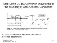
Fixed Off-Time Selection<br />
With increasing values of t OFF, switching losses decrease, lowlevel<br />
load current regulation improves, EMI reduces, PWM<br />
frequency decreases, and ripple current increases. The value of<br />
t OFF can be chosen for optimization of these parameters. For<br />
applications where audible noise is a concern, typical values of<br />
t OFF should be chosen in the range of 15 to 35 s.<br />
Allegro MicroSystems, Inc.<br />
115 Northeast Cutoff, Box 15036<br />
Worcester, Massachusetts 01615-0036 (508) 853-<br />
5000<br />
www.allegromicro.com<br />
7