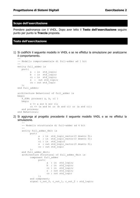
Progettazione di Sistemi Digitali Esercitazione 2 Scopo dell ...
Progettazione di Sistemi Digitali Esercitazione 2 Scopo dell ...
Progettazione di Sistemi Digitali Esercitazione 2 Scopo dell ...

You also want an ePaper? Increase the reach of your titles
YUMPU automatically turns print PDFs into web optimized ePapers that Google loves.
<strong>Progettazione</strong> <strong>di</strong> <strong>Sistemi</strong> <strong>Digitali</strong> <strong>Esercitazione</strong> 2<br />
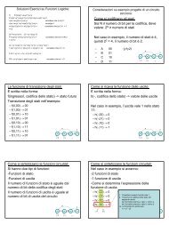
<strong>Scopo</strong> <strong>dell</strong>’esercitazione<br />
Prendere padronanza con il VHDL. Dopo aver letto il Testo <strong>dell</strong>’esercitazione seguire<br />
punto per punto la Traccia proposta.<br />
Testo <strong>dell</strong>’esercitazione<br />
1) Si co<strong>di</strong>fichi il seguente mo<strong>dell</strong>o in VHDL e se ne effettui la simulazione per analizzarne<br />
il comportamento.<br />
--<br />
-- Mo<strong>dell</strong>o comportamentale <strong>di</strong> full-adder ad 1 bit<br />
--<br />
entity full_adder is<br />
port(<br />
a : in std_logic;<br />
b : in std_logic;<br />
ci : in std_logic;<br />
s : out std_logic;<br />
co : out std_logic<br />
);<br />
end full_adder;<br />
architecture Behavioral of full_adder is<br />
begin<br />
P_SUM: process( a, b, ci )<br />
begin<br />
s
<strong>Progettazione</strong> <strong>di</strong> <strong>Sistemi</strong> <strong>Digitali</strong> <strong>Esercitazione</strong> 2<br />
begin<br />
U1: full_adder port map ( a(0), b(0), ci, s(0), c_out_0 );<br />
U2: full_adder port map ( a(1), b(1), c_out_0, s(1), c_out_1 );<br />
U3: full_adder port map ( a(2), b(2), c_out_1, s(2), c_out_2 );<br />
U4: full_adder port map ( a(3), b(3), c_out_2, s(3), co );<br />
end Structural;<br />
Traccia<br />
Per lo svolgimento <strong>dell</strong>’esercitazione è necessario seguire i passi qui riportati:<br />
1. Lanciare il Project Navigator<br />
2. Selezionare File New Project<br />
3. Riempire i seguenti campi dopo<strong>di</strong>ché premere Avanti<br />
a. Project Name: esercitazione2<br />
b. Project Location: in<strong>di</strong>care un percorso nella propria home<br />
c. Top-Level Module Type: HDL<br />
4. Riempire i seguenti campi dopo<strong>di</strong>ché premere Avanti<br />
a. Device Family: Spartan2 per la scheda Pegasus, Spartan3 per la scheda S3<br />
b. Device: xc2s50 per la scheda Pegasus, xc3s200 per la scheda S3<br />
c. Package: pq208 per la scheda Pegasus, ft256 per la scheda S3<br />
d. Speed Grade: -6 per la scheda Pegasus, -4 per la scheda S3<br />
5. Continuare a premere Avanti fino a che non si arriva alla chiusura <strong>dell</strong>a finestra <strong>di</strong><br />
<strong>di</strong>alogo<br />
6. Nella finestra Sources In Project selezionare xc2s50-6pq208 per la scheda Pegasus,<br />
xc3s200-4ft256 per la scheda S3<br />
7. Premere il tasto destro del mouse e selezionare New Source<br />
8. Nella finestra New Source<br />
a. Selezionare la voce VHDL Module<br />
b. Compilare il campo File Name con full_adder<br />
c. Continuare a premere Avanti fino a che non si arriva alla chiusura <strong>dell</strong>a<br />
finestra <strong>di</strong> <strong>di</strong>alogo<br />
9. A questo punto verrà aperta una nuova finestra, contenente lo scheletro <strong>di</strong> un<br />
mo<strong>dell</strong>o VHDL. Si ricopi in tale finestra il co<strong>di</strong>ce VHDL <strong>dell</strong>’esercizio1 e si salvi il file<br />
10. Si effettui la simulazione come visto nella esercitazione 1 (pagina 3)<br />
11. Si implementi il sommatore a 4 bit sulla scheda in dotazione, utilizzando gli 8 switch<br />
come input e 5 led come output. Si ricopi lo scheletro del co<strong>di</strong>ce VHDL<br />
<strong>dell</strong>’esercizio2 e si salvi il file<br />
12. Si proceda come nell’esercizio1 con la simulazione e la verifica del risultato ottenuto