CIRCUITI LOGICI •Circuiti combinatori •Circuiti sequenziali •PLD ...
CIRCUITI LOGICI •Circuiti combinatori •Circuiti sequenziali •PLD ...
CIRCUITI LOGICI •Circuiti combinatori •Circuiti sequenziali •PLD ...

Create successful ePaper yourself
Turn your PDF publications into a flip-book with our unique Google optimized e-Paper software.
<strong>•Circuiti</strong> <strong>combinatori</strong><br />
<strong>•Circuiti</strong> <strong>sequenziali</strong><br />
<strong>•PLD</strong><br />
•CPLD<br />
•FPGA<br />
ELETTRONICA DIGITALE<br />
<strong>CIRCUITI</strong> <strong>LOGICI</strong>
Logica booleana<br />
Teoremi fondamentali:<br />
A + A * B = A; A * (A + B) = A<br />
XY + X’Z + YZ = XY + X’Z<br />
DeMorgan: (x + y)’ = x’y’; (xy)’ = x’ + y’<br />
DeMorgan generalizzato: [ f (x 1, x 2, …, x n, 0, 1, +, * ) ]’ =<br />
f (x 1’, x 2’, …, x n’, 1, 0, *, + )<br />
Minimizzazione logica: mappe di Karnaugh<br />
– Minimizzare F = A’B + A’C + A’D + ACD<br />
– F = A’B (C’D’ + C’D + CD’ + CD)<br />
+ A’C (B’D’ + B’D + BD’ + BD)<br />
+ A’D (B’C’ + B’C + BC’ + BC)<br />
+ ACD (B’ + B)<br />
= A’BC’D’ + A’BC’D + A’BCD’ + A’BCD + …<br />
--> forma canonica sum-of-products (SOP)<br />
2
Mappe di Karnaugh<br />
– Coprire la mappa e risolvere<br />
– Il risultato dovrebbe essere F = CD + A’B + A’C + A’D<br />
CD<br />
AB<br />
00<br />
01<br />
11<br />
10<br />
C<br />
D<br />
A'<br />
B<br />
A'<br />
C<br />
A'<br />
D<br />
(4)<br />
(1)<br />
00 01 11 10<br />
1<br />
1 1<br />
1<br />
1<br />
1<br />
1<br />
1<br />
1<br />
F<br />
(3)<br />
(2)<br />
Implement<br />
using<br />
NAND<br />
gates<br />
only<br />
C<br />
D<br />
A'<br />
B<br />
A'<br />
C<br />
A'<br />
D<br />
(1) (2) (3) (4)<br />
Implement<br />
using 2-input<br />
NAND gates<br />
only.<br />
F<br />
3
• Insiemi di gate funzionalmente completi<br />
– { OR, AND, NOT}<br />
– { OR, NOT}<br />
– { AND, NOT }<br />
– NAND e NOR sono gate universali<br />
A + BC + DE'F<br />
A<br />
B<br />
C<br />
D<br />
E'<br />
F<br />
A<br />
B<br />
C<br />
D<br />
E'<br />
F<br />
Realizzazione mediante gate<br />
A<br />
B<br />
C<br />
D<br />
E'<br />
F<br />
4
• Implementazione mediante gate:<br />
Progetto di logica <strong>combinatori</strong>a<br />
– AND-OR, NAND-NAND, OR-AND, NOR-NOR, …<br />
• Altri Gates SSI<br />
– XOR, XNOR, buffer, tri-state buffer, wired-AND<br />
• Dispositivi MSI<br />
– MUX, DEMUX, Decoder, Encoder, Priority Encoder,<br />
– Adder, Buffer, Comparator,<br />
– Parity Generator, Parity Checker, …<br />
• Implementazione mediante MUX:<br />
I1<br />
I0<br />
sel<br />
Out<br />
Implementazione AND-OR<br />
I1<br />
I0<br />
sel<br />
Out<br />
Implementazione Three-state<br />
5
Progetto di logica <strong>combinatori</strong>a (2)<br />
• Qualunque funzione di k variabili puo` essere implementata<br />
con MUX a 2 k vie<br />
• Qualunque funzione di k variabili puo` essere implementata con<br />
un decoder da k a 2 k e porte NAND<br />
x<br />
y<br />
0<br />
1<br />
x<br />
2 - 1 MUX<br />
I1<br />
I0<br />
sel<br />
Out<br />
f = x' :<br />
2 - 4 Decoder<br />
I1<br />
I0<br />
O3<br />
O2<br />
O1<br />
O0<br />
x<br />
x'<br />
y<br />
2 - 1 MUX<br />
I1<br />
I0<br />
sel<br />
Out<br />
f = x'y' + xy:<br />
f = x'y' + xy:<br />
6
Il circuito SW-SW e’<br />
generalizzabile con una rete<br />
di interruttori in parallelo<br />
verso Gnd ed una rete di<br />
interruttori in serie verso<br />
Val collegati agli ingressi<br />
IN1, IN2, INn<br />
In questo modo si realizza<br />
la funzione logica NOR<br />
IN1<br />
IN2<br />
INn<br />
IN1<br />
IN2<br />
INn<br />
OUT = IN1 + IN2 .. + ... INn<br />
Gate CMOS<br />
Val<br />
Gnd<br />
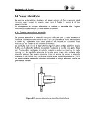
I CALCOLI DELLA POTENZA DISSIPATA E DEL<br />
RITARDO SONO GLI STESSI DEL’INVERTER<br />
OUT<br />
...<br />
...<br />
7
Se la rete superiore ha gli<br />
SW in parallelo e la rete<br />
inferiore ha gli SW in serie<br />
si realizza la funzione<br />
logica NAND<br />
OUT = IN1 IN2 .. ... INn<br />
IN1<br />
IN2<br />
INn<br />
IN1<br />
IN2<br />
INn<br />
Gate CMOS (2)<br />
Val<br />
Gnd<br />
I CALCOLI DELLA POTENZA DISSIPATA E DEL<br />
RITARDO SONO GLI STESSI DEL’INVERTER<br />
OUT<br />
...<br />
...<br />
8
Realizzare la<br />
funzione logica<br />
OUT = C + ( A B )<br />
SUGGERIMENTO:<br />
USARE LE LEGGI DI<br />
DE MORGAN!!<br />
A<br />
B<br />
C<br />
Gate CMOS: esempio<br />
Val<br />
Gnd<br />
Calcolare Tf e Tr nelle diverse configurazioni degli<br />
ingressi<br />
OUT<br />
(Tutte le resistenze degli switch sono uguali a RSWU e<br />
RSWd )<br />
A<br />
B<br />
C<br />
B<br />
A C<br />
A B<br />
C<br />
9
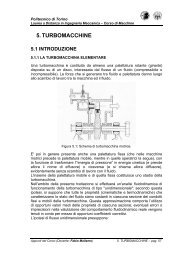
Struttura generale di un circuito sequenziale<br />
Circuiti <strong>sequenziali</strong><br />
•Tipi di circuiti <strong>sequenziali</strong>:<br />
–Sequenziali asincroni:<br />
lo stato puo` cambiare<br />
in ogni istante<br />
–Sequenziali sincroni:<br />
lo stato puo` cambiare<br />
solo in modo sincrono<br />
con il clock<br />
10
Latch S-R<br />
11
Latch e flip-flop tipo D<br />
12
Tempistica del flip-flop<br />
DATO UN FLIP FLOP DI TIPO D SI DICE CHE “SUL FRONTE DI<br />
SALITA DEL CLOCK SI CAMPIONA L’INGRESSO D CHE VIENE<br />
MEMORIZZATO IN USCITA” ..... MA COSA SUCCEDE SE D CAMBIA<br />
PROPRIO SUL FRONTE DEL CLOCK?<br />
CK<br />
D<br />
Q<br />
Qn<br />
METASTABILITA`<br />
L’USCITA NON VARIA COME PREVISTO; PUO’<br />
OSCILLARE ANCHE PER LUNGO TEMPO!<br />
13
Tempi di set-up e hold<br />
IL CAMPIONAMENTO DEL DATO D E’ COME FARE UNA FOTO; SE IL<br />
SOGGETTO SI MUOVE MENTRE SI SCATTA LA FOTO RIMANE MOSSA...<br />
COME PER LE FOTO E’ NECESSARIO CHE D NON CAMBI DURANTE IL<br />
FRONTE DEL CLOCK:<br />
Tsu = TEMPO (DI SET-UP ) PRIMA DEL FRONTE IN CUI D NON DEVE<br />
VARIARE<br />
Th = TEMPO (DI HOLD) DOPO IL FRONTE IN CUI D NON DEVE VARIARE<br />
CK<br />
D<br />
Tsu Th<br />
14
Rimedi alla metastabilita`<br />
• La metastabilita` non puo` essere eliminata<br />
completamente<br />
• Si puo` pero` ridurre la probabilita` di insorgenza del<br />
fenomeno<br />
– Soluzioni per ingressi asincroni<br />
1. Avere dati di ingresso con transizioni rapide<br />
2. Passare I dati in parecchi flip-flop prima di usarli<br />
15
1. Macchina di Mealy:<br />
Macchine a stati finiti<br />
» Le uscite dipendono dagli ingressi attuali e dallo<br />
stato presente<br />
2. Macchina di Moore:<br />
» Le uscite dipendono solo dallo stato presente<br />
• Passi di progetto per una FSM<br />
1. Disegnare il diagramma degli stati<br />
2. Assegnare gli stati<br />
3. Ottenere la tabella delle transizioni degli stati<br />
4. Ricavare le equazioni logiche<br />
5. Disegnare il circuito logico<br />
ESEMPIO: contatore sincrono binario a 3 bit<br />
16
Diagramma degli stati:<br />
Esempio<br />
Assegnazione degli stati e<br />
tabella delle transizioni<br />
17
Equazioni per lo stato futuro:<br />
Circuito logico:<br />
Esempio (2)<br />
18
• n-bit Register<br />
• Shift Register<br />
• Contatore ripple carry<br />
Circuiti <strong>sequenziali</strong> MSI<br />
19
Introduzione alle PLD<br />
DALL’INIZIO DEGLI ANNI 80 SONO STATI PRODOTTI <strong>CIRCUITI</strong> INTEGRATI<br />
“PROGRAMMABILI” (PROGRAMMABLE LOGIC DEVICES - PLD -) , IN CUI<br />
L’UTENTE “PROGRAMMA” LE FUNZIONI LOGICHE DENTRO IL CHIP<br />
(HARDWARE PROGRAMMATO VIA SOFTWARE!)<br />
NEL CHIP ESISTONO ARRAY DI GATE (COMBINATORI E FF) CON LE<br />
INTERCONNESSIONI PROGRAMMABILI (IN MODO PERMANENTE O<br />
TEMPORANEO). LE FUNZIONI LOGICHE SI BASANO SUL CONCETTO DEL<br />
WIRED-OR PER CUI L’OPERAZIONE LOGICA AVVIENE TRA TUTTI GLI<br />
INGRESSI CONNESSI<br />
• Tipi di Programmable Logic Devices (PLDs)<br />
– Programmable Logic Array (PLA)<br />
– Programmable AND-Array Logic (PAL)<br />
– PROM e EPROM<br />
– Generic Array Logic (GAL)<br />
– Complex PLD (CPLD)<br />
– Field Programmable Gate Array (FPGA)<br />
20
Struttura logica di una PLA<br />
Programmable Connections Product Terms Programmable Connections<br />
Problema: troppe connessioni programmabili<br />
Sum of Products Expressions<br />
21
I1<br />
ESEMPIO DI PROGRAMMAZIONE<br />
CHE FUNZIONI REALIZZANO LE USCITE DELLA PLD?<br />
I2 I3 I4<br />
O1 O2 O3 O4<br />
O1 = I2 I3 + I3 I4 ; O2 = I1 I4 + I1 I2 ; O3 = I1 I2 ; O4 = I2 I3 + I1 I4<br />
22
Programmazione delle connessioni<br />
23
Sum of Products (SoP)<br />
A B C<br />
AND plane<br />
Struttura di una PAL <strong>combinatori</strong>a<br />
Piano AND programmabile<br />
Piano OR fisso (nr. Ingressi variabile)<br />
f1 = A • B • C + A • B • C<br />
f2 = A • B + A • B • C<br />
24
PAL18L4<br />
25
• Esempio: Z 0 = A’BC + C’D<br />
PAL18L4: esempio<br />
– Z 0’ = (A + B’ + C’) (C + D’)<br />
= AC + B’C + AD’ + B’D’ + C’D’<br />
26
PAL registrate<br />
Possono implementare strutture <strong>combinatori</strong>e e <strong>sequenziali</strong><br />
A B C<br />
To AND plane<br />
Clock<br />
Flip-flop<br />
D Q<br />
Select<br />
MUX<br />
Enable<br />
f1<br />
27
PAL16R8<br />
Configurata come<br />
contatore a tre bit, in<br />
codice di Gray<br />
Le GAL sono versioni<br />
riprogrammabili delle PAL<br />
registrate<br />
Example: GAL16V8R<br />
–GAL configured as a<br />
“PAL16R8 type” device<br />
–8 of the 16 inputs come<br />
from the D flip-flop outputs<br />
28
Esempio: 22V10<br />
29
• Struttura logica di una PROM<br />
canonical SOPs<br />
Uso di PROM e EPROM<br />
minterms<br />
30
Uso di PROM e EPROM (2)<br />
• Esempio: Uso di una PROM 256 x 4 ,<br />
– Implementare f1 = w’xy’+x’yz’ + xz<br />
e f2 = a’b’y + abx’y’ + a’bx’y’<br />
31
Concetto generale: molte PLD in un unico IC<br />
•Piu` product terms;<br />
•Piu` risorse di<br />
routing;<br />
•Piu` macro celle;<br />
•Piu` connettivita` fra<br />
macro celle<br />
(possibilita` di<br />
implementare funzioni<br />
piu` complesse).<br />
I/O block I/O block<br />
CPLD<br />
PLD block PLD block<br />
Interconnection wires<br />
PLD block PLD block<br />
I/O block I/O block<br />
32
I/O<br />
Global<br />
Tri-States<br />
JTAG Port<br />
I/O<br />
I/O<br />
I/O<br />
Global<br />
Clocks<br />
Global<br />
Set/Reset<br />
3<br />
3<br />
1<br />
2 or 4<br />
JTAG<br />
Controller<br />
I/O<br />
Blocks<br />
Esempio di CPLD: Xilinx XC9500<br />
In-System<br />
Programming Controller<br />
FastCONNECT<br />
Switch Matrix<br />
Function<br />
Block 1<br />
Function<br />
Block 2<br />
Function<br />
Block 3<br />
Function<br />
Block 4<br />
• 5 volt in-system<br />
programmable<br />
(ISP) CPLDs<br />
• 5 ns pin-to-pin<br />
• 36 to 288<br />
macrocells<br />
(6400 gates)<br />
• 10,000<br />
program/erase<br />
cycles<br />
• Complete IEEE<br />
1149.1 JTAG<br />
capability<br />
33
Caratteristiche dell’architettura XC9500<br />
• Uniform, all pins fast, PAL-like architecture<br />
• FastCONNECT switch matrix provides 100% routing<br />
with 100% utilization<br />
• Flexible function block<br />
– 36 inputs with 18 outputs<br />
– Expandable to 90 product terms per macrocell<br />
– Product term and global three-state enables<br />
– Product term and global clocks<br />
– Product term and global set/reset signals<br />
• 3.3V/5V I/O operation<br />
• Complete IEEE 1149.1 JTAG interface<br />
34
36<br />
From<br />
FastCONNECT<br />
To<br />
FastCONNECT<br />
AND<br />
Array<br />
XC9500: blocco funzionale<br />
Product-<br />
Term<br />
Allocator<br />
Global 3<br />
Clocks<br />
Macrocell 1<br />
Macrocell 18<br />
Global<br />
Tri-State<br />
2 or 4<br />
Ogni blocco funzionale e` come una 36V18 !<br />
I/O<br />
I/O<br />
35
Esempio: Altera Max 7000<br />
36
Esempio: Altera Max 7000 (2)<br />
37
FIELD PROGRAMMABLE GATE ARRAY (FPGA)<br />
DALLE PRIME PLD AD OGGI L’INTEGRAZIONE HA PERMESSO DI<br />
REALIZZARE <strong>CIRCUITI</strong> <strong>LOGICI</strong> PROGRAMMABILI MOLTO COMPLESSI. SI<br />
CHIAMANO FIELD-PROGRAMMABLE-GATE-ARRAY (FPGA) E STANNO<br />
RIMPIAZZANDO I <strong>CIRCUITI</strong> REALIZZATI CON LE FAMIGLIE LOGICHE<br />
TRADIZIONALI IN NUMEROSE APPLICAZIONI.<br />
INTERCONNESSIONI<br />
PROGRAMMABILI<br />
CELLE LOGICHE<br />
PROGRAMMABILI<br />
CELLE DI I/O<br />
PROGRAMMABILI<br />
38
FAMIGLIE LOGICHE AVANZATE<br />
FPGA<br />
AD OGGI SONO DISPONIBILI SUL MERCATO FPGA CON DIVERSI MILIONI DI<br />
GATE PROGRAMMABILI E CON DIVERSE CENTINAIA DI KBIT DI MEMORIA.<br />
LAVORANO A CENTINAIA DI MHz CON PIU’ DI 500 PIN DI I/O<br />
DEVICE<br />
XCV200E<br />
XCV600E<br />
XCV2000E<br />
XCV3200E<br />
SYSTEM<br />
GATES<br />
214.640<br />
985.882<br />
2.541.952<br />
4.074.387<br />
LOGIC<br />
GATES<br />
63.504<br />
186.624<br />
518.400<br />
876.096<br />
DIFF I/O<br />
PAIRS<br />
119<br />
247<br />
344<br />
344<br />
USER I/O<br />
284<br />
512<br />
804<br />
804<br />
BLOCK<br />
RAM Bits<br />
114.688<br />
294.912<br />
655.360<br />
851.968<br />
DISTRIB.<br />
RAM Bits<br />
75.264<br />
221.184<br />
614.400<br />
1.038.336<br />
39
I/O block<br />
Logic block Interconnection switches<br />
I/O block<br />
I/O block<br />
FPGA: struttura generale<br />
I/O block<br />
In 1<br />
In 2<br />
In 3<br />
In 4<br />
Blocco logico base<br />
LUT<br />
Clock<br />
Flip-flop<br />
D Q<br />
Select<br />
La Look-up-table puo` essere usata:<br />
1. Funzione booleana di 4 ingressi<br />
2. Memoria 16x1<br />
40<br />
Out
A<br />
B<br />
C<br />
D<br />
A<br />
B<br />
C<br />
D<br />
Esempio: funzione di 4 variabili<br />
Out<br />
Out<br />
A B C D Out<br />
0 0 0 0 0<br />
0 0 0 1 1<br />
0 0 1 0 1<br />
0 0 1 1 1<br />
0 1 0 0 0<br />
0 1 0 1 1<br />
0 1 1 0 1<br />
0 1 1 1 1<br />
1 0 0 0 0<br />
1 0 0 1 1<br />
1 0 1 0 1<br />
1 0 1 1 1<br />
1 1 0 0 0<br />
1 1 0 1 0<br />
1 1 1 0 0<br />
1 1 1 1 0<br />
41
LB<br />
LB<br />
Interconnessioni programmabili<br />
Switch<br />
Matrix<br />
LB<br />
LB<br />
Switch<br />
Matrix<br />
LB<br />
LB<br />
42
Funzionamento delle switch matrix<br />
Prima della programmazione Dopo la programmazione<br />
43
Differenze CPLD - FPGA<br />
CPLD FPGA<br />
Complex Programmable Logic Device Field-Programmable Gate Array<br />
Architecture PAL/22V10-like Gate array-like<br />
More Combinational More Registers + RAM<br />
Density Low-to-medium Medium-to-high<br />
0.5-10K logic gates 1K to 1M system gates<br />
Performance Predictable timing Application dependent<br />
Up to 250 MHz today Up to 150MHz today<br />
Interconnect “Crossbar Switch” Incremental<br />
44
FPGA a grana fine e grossa<br />
Grana grossa (tecnologia SRAM) – per es. Altera, Xilinx<br />
• Blocchi logici grandi e complessi<br />
• Funzioni dedicate (per es. RAM o catene di propagazione del carry)<br />
• Riprogrammabili<br />
• Ritardi di propagazione non predicibili<br />
Grana fine (tecnologia Antifuse) – per es. Actel<br />
• Blocchi logici piccoli<br />
• Ritardi di propagazione predicibili<br />
• Velocita` superiori<br />
• One time programmable (OTP)<br />
45
Switch<br />
Matrix<br />
FPGA - Xilinx 4000 Series – struttura<br />
CLB<br />
CLB CLB CLB<br />
CLB CLB CLB CLB<br />
CLB CLB CLB CLB<br />
CLB<br />
CLB<br />
CLB<br />
Single length<br />
CLB<br />
I/O blocks<br />
Long<br />
lines<br />
46
FPGA - Xilinx 4000 Series - CLB<br />
47
FPGA - Xilinx 4000 Series – CLB<br />
Two 4-input function generators (F and G) offer unrestricted versatility (most <strong>combinatori</strong>al<br />
logic functions need four or fewer inputs). A third function generator, labeled H’, can<br />
implement any Boolean function of its three inputs.<br />
The CLB storage elements can be configured as latches or flip-flops, positive or negative<br />
edge triggered. An asynchronous storage element input (SR) can be configured as either<br />
set or reset. This configuration option determines the state in which each flip-flop becomes<br />
operational after configuration.<br />
Multiplexers in the CLB map the four control inputs (C1 - C4) into the four internal control<br />
signals (H1, DIN/H2, SR/H0, and EC). Any of these inputs can drive any of the four<br />
internal control signals.<br />
Optional modes for each CLB make the memory look-up tables in the F’ and G’ function<br />
generators usable as an array of Read/Write memory cells. Depending on the selected<br />
mode, a single CLB can be configured as either a 16x2, 32x1, or 16x1 bit array.<br />
The F1-F4 and G1-G4 inputs to the function generators act as address lines, selecting a<br />
particular memory cell in each look-up table. The DIN/H2, H1, and SR/H0 lines become<br />
the two data inputs (D0, D1) and the Write Enable (WE) input for the 16x2 memory. When<br />
the 32x1 configuration is selected, D1 acts as the fifth address bit and D0 is the data input.<br />
48
FPGA - Xilinx 4000 Series – IO block<br />
49
Segnali di ingresso<br />
FPGA - Xilinx 4000 Series – IO block<br />
User-configurable input/output blocks (IOBs) provide the interface between external<br />
package pins and the internal logic.<br />
Each IOB controls one package pin and can be configured for input, output, or<br />
bidirectional signals.<br />
Two paths, labeled I1 and I2, bring input signals into the array. Inputs also connect to an<br />
input register that can be programmed as either an edge-triggered flip-flop or a levelsensitive<br />
latch.<br />
The data input to the register can optionally be delayed by several nanoseconds. With the<br />
delay enabled, the setup time of the input flip-flop is increased so that normal clock routing<br />
does not result in a positive hold-time requirement. The delay guarantees a zero hold time<br />
with respect to clocks routed through any of the global clock buffers.<br />
An additional optional latch on the input is clocked by the output clock; this additional latch<br />
allows the very fast capture of input data, which is then synchronized to the internal clock<br />
by the IOB flip-flop or latch.<br />
50
Segnali di uscita<br />
FPGA - Xilinx 4000 Series – IO block<br />
Output signals can be optionally inverted within the IOB, and can pass directly to the pad<br />
or be stored in an edge-triggered flip-flop.<br />
An active-High 3-state signal can be used to place the output buffer in a high-impedance<br />
state, implementing 3-state outputs or bidirectional I/O.<br />
FPGAs can directly drive buses on a printed circuit board, since a guaranteed output sink<br />
current of 12 mA is given. The output pull-up structure can be configured as a TTL-like<br />
totem-pole or as CMOS drivers, with p-channel pull-up transistors pulling to Vcc.<br />
A multiplexer can be configured as a 2-input function generator, implementing a passgate,<br />
AND-gate, OR-gate, or XOR-gate, with 0, 1, or 2 inverted inputs:<br />
•When configured as a multiplexer, this feature allows two output signals to time-share the<br />
same output pad, effectively doubling the number of device outputs without requiring a<br />
larger, more expensive package.<br />
•When the MUX is configured as a 2-input function generator, logic can be implemented<br />
within the IOB itself, so allowing for very high-speed gating of a single signal.<br />
51
FPGA - Xilinx 4000 Series – routing<br />
• 1) Fast Direct Interconnect - CLB to CLB<br />
• 2) General Purpose Interconnect - Uses switch matrix<br />
• 3) Long Lines<br />
– Segmented across<br />
chip<br />
– Global clocks, lowest<br />
skew<br />
– 2 Tri-states per CLB<br />
for busses<br />
• Other routing types in<br />
CPLDs<br />
Switch<br />
Matrix<br />
CLB CLB<br />
CLB CLB<br />
Switch<br />
Matrix<br />
CLB CLB<br />
CLB CLB<br />
52
FPGA - Xilinx 4000 Series – altre risorse<br />
• Tri-state buffers for busses (BUFT’s)<br />
• Global clock & high speed buffers<br />
(BUFG’s)<br />
• Wide Decoders (DECODEx)<br />
• Internal Oscillator (OSC4)<br />
• Global Reset to all Flip-Flops,<br />
Latches (STARTUP)<br />
• CLB special resources<br />
– Fast Carry logic built into CLBs<br />
– Synchronous Dual Port RAM<br />
– Boundary Scan<br />
53
FPGA - Altera FLEX 10K - struttura<br />
54
FPGA - Altera FLEX 10K – Logic Element<br />
FLEX 10K Series Logic Element (LE), from Altera FLEX 10K data sheet<br />
55
Embedded<br />
Array Block<br />
(EAB)<br />
FPGA - Altera FLEX 10K - EAB<br />
56
Esempio di FPGA a grana fine - Actel SX - struttura<br />
57
FPGA Example - Actel SX Family – celle R e C<br />
Cella C Cella R<br />
58
Tecnologia delle interconnessioni<br />
Static Random Access Memory (SRAM)<br />
• ogni switch e` un pass transistor controllato dallo stato di una cella SRAM<br />
• Richiede una PROM per configurare la FPGA al power-on<br />
Electrically Erasable Programmable ROM (EPROM)<br />
• ogni switch e` un transistor floating-gate. Il codice di configurazione e`<br />
residente nella FPGA<br />
• Riprogrammabile, anche in-circuit (ISP/JTAG)<br />
Fusible Links - one time programmable (“Antifuse”)<br />
• Quando e` programmato elettricamente, forma un percorso a bassa<br />
resistenza<br />
• one-time programmable, mediante hardware apposito<br />
• radiation tolerant<br />
59
Esempio di FPGA - Actel SX Family<br />
Architettura tipo “sea-of-modules”<br />
Tutto il dispositivo e` coperto da una<br />
griglia di moduli logici<br />
Le risorse di routing and interconnessione<br />
stanno sotto la griglia<br />
from Actel’s SX Family of FPGA’s - Technology Backgrounder<br />
60
Tagli tipici<br />
No of I/O No of regs Memory<br />
Altera 20K30E-2 128 1200 24 Kbits<br />
Altera 20K200E-1 376 8320 100 Kbits<br />
Altera EP2A15C7 492 16640 450 Kbits<br />
Xilinx XC2S15-5 86 384 16 Kbits<br />
Xilinx XC2S200-5 284 4704 57 Kbits<br />
Xilinx XC2V3000 684 28672 1728 Kbits<br />
I prezzi dipendono anche dalla velocita`.<br />
(per es. La versione piu` veloce puo` essere piu` costosa del 50%).<br />
I dispositivi in tabella costano da $30 a $900. Una PLD a 32 registri<br />
costa da $2<br />
Serve anche il dispositivo di configurazione: Altera PROM: $8,<br />
EEPROM: $21<br />
61
1<br />
Flusso di progetto con FPGA - CPLD<br />
Design Entry in schematic, ABEL, VHDL,<br />
and/or Verilog. Vendors include Synopsys,<br />
Aldec (Xilinx Foundation), Mentor, Cadence,<br />
Viewlogic, and 35 others.<br />
M1 Technology<br />
*XC9500 has 20,000 write/erase cycles<br />
2<br />
Implementation includes Placement & Routing<br />
and bitstream generation using Xilinx’s M1<br />
Technology. Also, analyze timing, view layout,<br />
and more.<br />
Download directly to the Xilinx<br />
hardware device(s) with<br />
unlimited reconfigurations* !!<br />
XC4000<br />
3<br />
XC4000<br />
XC4000<br />
62
Flusso di progetto<br />
IL PROGETTO E LA PROGRAMMAZIONE AVVIENE MEDIANTE<br />
STRUMENTI CAD CON IL SEGUENTE DESIGN FLOW:<br />
Start<br />
DESIGN ENTRY PRELAYOUT SIMULATION<br />
LOGIC SYNTHESIS<br />
SYSTEM PARTITIONING<br />
FLOORPLANNING POSTLAYOUT SIMULATION<br />
PLACEMENT<br />
ROUTING CIRCUIT EXTRACTION<br />
PROGRAMMING<br />
End<br />
63