Etudes par microscopie en champ proche des phénomènes de ...
Etudes par microscopie en champ proche des phénomènes de ...
Etudes par microscopie en champ proche des phénomènes de ...

Create successful ePaper yourself
Turn your PDF publications into a flip-book with our unique Google optimized e-Paper software.
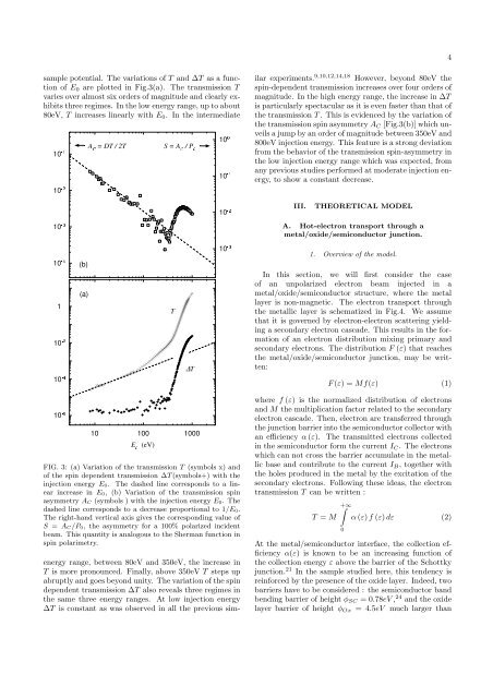
4sample pot<strong>en</strong>tial. The variations of T and ΔT as a functionof E 0 are plotted in Fig.3(a). The transmission Tvaries over almost six or<strong>de</strong>rs of magnitu<strong>de</strong> and clearly exhibitsthree regimes. In the low <strong>en</strong>ergy range, up to about80eV, T increases linearly with E 0 . In the intermediate<strong>en</strong>ergy range, betwe<strong>en</strong> 80eV and 350eV, the increase inT is more pronounced. Finally, above 350eV T steps upabruptly and goes beyond unity. The variation of the spin<strong>de</strong>p<strong>en</strong>d<strong>en</strong>t transmission ΔT also reveals three regimes inthe same three <strong>en</strong>ergy ranges. At low injection <strong>en</strong>ergyΔT is constant as was observed in all the previous similarexperim<strong>en</strong>ts. 9,10,12,14,18 However, beyond 80eV thespin-<strong>de</strong>p<strong>en</strong>d<strong>en</strong>t transmission increases over four or<strong>de</strong>rs ofmagnitu<strong>de</strong>. In the high <strong>en</strong>ergy range, the increase in ΔTis <strong>par</strong>ticularly spectacular as it is ev<strong>en</strong> faster than that ofthe transmission T . This is evid<strong>en</strong>ced by the variation ofthe transmission spin asymmetry A C [Fig.3(b)] which unveilsa jump by an or<strong>de</strong>r of magnitu<strong>de</strong> betwe<strong>en</strong> 350eV and800eV injection <strong>en</strong>ergy. This feature is a strong <strong>de</strong>viationfrom the behavior of the transmission spin-asymmetry inthe low injection <strong>en</strong>ergy range which was expected, fromany previous studies performed at mo<strong>de</strong>rate injection <strong>en</strong>ergy,to show a constant <strong>de</strong>crease.III.THEORETICAL MODELA. Hot-electron transport through ametal/oxi<strong>de</strong>/semiconductor junction.1. Overview of the mo<strong>de</strong>l.In this section, we will first consi<strong>de</strong>r the caseof an unpolarized electron beam injected in ametal/oxi<strong>de</strong>/semiconductor structure, where the metallayer is non-magnetic. The electron transport throughthe metallic layer is schematized in Fig.4. We assumethat it is governed by electron-electron scattering yieldinga secondary electron casca<strong>de</strong>. This results in the formationof an electron distribution mixing primary andsecondary electrons. The distribution F (ε) thatreachesthe metal/oxi<strong>de</strong>/semiconductor junction, may be writt<strong>en</strong>:F (ε) =Mf(ε) (1)FIG. 3: (a) Variation of the transmission T (symbols x) andof the spin <strong>de</strong>p<strong>en</strong>d<strong>en</strong>t transmission ΔT (symbols+) with theinjection <strong>en</strong>ergy E 0. The dashed line corresponds to a linearincrease in E 0, (b) Variation of the transmission spinasymmetry A C (symbols ) with the injection <strong>en</strong>ergy E 0.Thedashed line corresponds to a <strong>de</strong>crease proportional to 1/E 0.The right-hand vertical axis gives the corresponding value ofS = A C/P 0, the asymmetry for a 100% polarized incid<strong>en</strong>tbeam. This quantity is analogous to the Sherman function inspin polarimetry.where f (ε) is the normalized distribution of electronsand M the multiplication factor related to the secondaryelectron casca<strong>de</strong>. Th<strong>en</strong>, electron are transferred throughthe junction barrier into the semiconductor collector withan effici<strong>en</strong>cy α (ε). The transmitted electrons collectedin the semiconductor form the curr<strong>en</strong>t I C . The electronswhich can not cross the barrier accumulate in the metallicbase and contribute to the curr<strong>en</strong>t I B , together withthe holes produced in the metal by the excitation of thesecondary electrons. Following these i<strong>de</strong>as, the electrontransmission T canbewritt<strong>en</strong>:T = M∫+∞0α (ε) f (ε) dε (2)At the metal/semiconductor interface, the collection effici<strong>en</strong>cyα(ε) is known to be an increasing function ofthe collection <strong>en</strong>ergy ε above the barrier of the Schottkyjunction. 21 In the sample studied here, this t<strong>en</strong>d<strong>en</strong>cy isreinforced by the pres<strong>en</strong>ce of the oxi<strong>de</strong> layer. In<strong>de</strong>ed, twobarriers have to be consi<strong>de</strong>red : the semiconductor bandb<strong>en</strong>ding barrier of height φ SC =0.78eV , 24 and the oxi<strong>de</strong>layer barrier of height φ Ox =4.5eV much larger than


![[Diffusion-Limited Aggregation - A Model for Pattern Formation].](https://img.yumpu.com/52395246/1/190x245/diffusion-limited-aggregation-a-model-for-pattern-formation.jpg?quality=85)