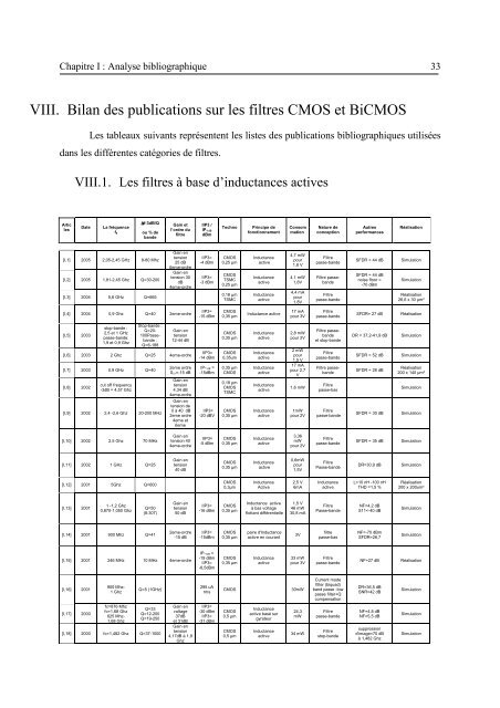
Chapitre I : Analyse bibliographique VIII. Bilan <strong>de</strong>s publications sur les filtres CMOS <strong>et</strong> BiCMOS Les tableaux suivants représentent les listes <strong>de</strong>s publications bibliographiques utilisées dans les différentes catégories <strong>de</strong> filtres. Artic les VIII.1. Les filtres à base d’inductances actives Date ∆f-3dB/Q La fréquence f0 ou % <strong>de</strong> ban<strong>de</strong> [I,1] 2005 2,05-2,45 GHz 8-80 Mhz [I,2] 2005 1,81-2,45 Ghz Q=30-200 [I,3] 2004 5,6 GHz Q=665 Gain <strong>et</strong> l’ordre du filtre Gain en tension 25 dB 6eme-ordre Gain en tension 30 dB 4eme-ordre [I,4] 2004 0,9 Ghz Q=40 2eme-ordre [I,5] 2003 stop-ban<strong>de</strong> : 2,5 <strong>et</strong> 1 GHz passe-ban<strong>de</strong>: 1,9 <strong>et</strong> 0,9 Ghz Stop-ban<strong>de</strong> : Q=20- 100Passeban<strong>de</strong> : Q=6-188 Gain en tension 12-44 dB [I,6] 2003 2 Ghz Q=25 4eme-ordre [I,7] 2003 0,9 GHz Q=40 [I,8] 2002 cut off frequency -3dB = 4,57 Ghz [I,9] 2002 2,4 -2,6 Ghz 20-200 MHz [I,10] 2002 2,5 Ghz 70 MHz [I,11] 2002 1 GHz Q=25 [I,12] 2001 5Ghz Q=600 [I,13] 2001 1 -1,2 Ghz 0,870-1,050 Ghz Q=50 (8-307) [I,14] 2001 900 Mhz Q=41 2eme ordre S21=-15 dB Gain en tension 4,34 dB 4eme-ordre Gain en tension <strong>de</strong> 0 à 40 dB 2eme ordre 4eme <strong>et</strong> 6eme Gain en tension 40 4eme-ordre Gain en tension 40 dB Gain en tension 50 dB 2eme-ordre -15 dB [I,15] 2001 246 MHz 10 MHz 4eme-ordre [I,16] 2001 [I,17] 2000 900 Mhz- 1 Ghz fc=876 Mhz fc=1,68 Ghz 625 Mhz- 1,68 Ghz Q=5 (1GHz) Q=33 Q=12-200 Q=19-250 [I,18] 2000 fc=1,482 Ghz Q=37-1000 Gain en voltage 37dB <strong>et</strong> 31dB Gain en tension 4,17dB à 1,9 Ghz IIP3 / IP-1dB dBm IIP3= -4 dBm IIP3= -3 dBm IIP3= -15 dBm IIP3= -14 dBm IP-1dB = -15dBm IIP3= -20 dBV IIP3= -5 dBm IIP3= -16 dBm IIP3= -15dBm IP-1dB = -19 dBm IIP3= -8,5dBm 295 uA rms IIP3= -30 dBm IIP3= -31 dBm Techno CMOS 0,25 µm CMOS TSMC 0,25 µm 0,18 µm TSMC CMOS 0,35 µm CMOS 0,35 µm CMOS 0,35um 0,35 µm CMOS 0,18 µm CMOS TSMC CMOS 0,35 µm CMOS 0,35 µm CMOS 0,35 µm CMOS 0,3µm CMOS 0,35 µm CMOS 0,35 µm CMOS 0,35 µm Principe <strong>de</strong> fonctionnement Inductance active Inductance active Inductance active Inductance active Inductance active Inductance active Inductance active Inductance active Inductance active Inductance active Inductance active Inductance Active Inductance active à bas voltage flottant différentielle paire d'Inductance active en courant Inductance active Consom mation 4,7 mW pour 1,8 V 4,1 mW 1,8V 4,4 mA pour 1,8V 17 mA pour 3V 2,8 mW pour 2V 2 mW pour 1,5 V 17 mA pour 2,7 V 1,6 mW 1mW pour 2V 3,36 mW pour 2V 0,6mW pour 1,5V 2,5 V 6mA 1,5 V 46 mW 30,8 mA 3V 33 mW pour 3V CMOS 30mW CMOS 0,5 µm CMOS 0,5 µm Inductance active basé sur gyrateur Inductance active 24,3 mW 34 mW Nature <strong>de</strong> <strong>conception</strong> Filtre passe-ban<strong>de</strong> Filtre passeban<strong>de</strong> Filtre passe-ban<strong>de</strong> Filtre passe-ban<strong>de</strong> Filtre passeban<strong>de</strong> <strong>et</strong> stop-ban<strong>de</strong> Filtre passe-ban<strong>de</strong> Filtre passeban<strong>de</strong> Filtre passe-bas Filtre passe-ban<strong>de</strong> Filtre passe-ban<strong>de</strong> Filtre Passe-ban<strong>de</strong> Inductance active Filtre Passe-ban<strong>de</strong> filtre passe-bas Filtre passe-ban<strong>de</strong> Current mo<strong>de</strong> filter (biquad) band passe -low passe filter+Q compensation Filtre passe-ban<strong>de</strong> Filtre stop-ban<strong>de</strong> Autres performances Réalisation SFDR = 44 dB Simulation SFDR = 44 dB noise floor = -70 dBm Simulation Réalisation 26,6 x 30 µm² SFDR= 27 dB Réalisation DR = 37,2-41,9 dB Simulation SFDR = 52 dB Simulation SFDR = 28 dB Réalisation 200 x 140 µm² Simulation SFDR = 30 dB Simulation SFDR = 35 dB Simulation DR=30,9 dB Simulation L=10 nH -100 nH THD =1,5 % NF=4,2 dB S11
Chapitre I : Analyse bibliographique [I,19] 2000 [I,20] 2000 [I,21] 2000 fc=1,098 Ghz <strong>de</strong> 595Mhz à1354 Mhz fc=1,089Ghz <strong>de</strong> 595Mhz à 1354Mhz 1,007 Ghz- 1,023 Ghz 8 Mhz=0,7% 8Mhz=0,7% Q=1000- 12000 [I,22] 2000 900 Mhz Q élevé Gain en tension 4,75dB Gain en tension 4,75 dB 2eme-ordre [I,23] 2000 400 Mhz 4eme-ordre [I,24] 1999 [I,25] 1999 [I,26] 1999 [I,27] 1998 [I,28] 1998 [I,29] 1998 Articles fc pass-ban<strong>de</strong> = 1,5Ghz fc pass-bas = 2,07Ghz <strong>de</strong> 1Ghz à 2,3 Ghz fc=2,07 Ghz 1,26 Ghz-2,3Ghz fc=881 Mhz 559Mhz- 970Mhz fc=1,5 Ghz 1-1,7 Ghz fc=900 Mhz 890 Mhz- 1,3 Ghz 900 Mhz - 1 Ghz Q=4,45-980 ∆f=15,7Mhz Q=4,8-1000 Q=10-1256 Q=31 10-1256 Qc=34 Q>400 Q=300 Q=20-100 Q=56-150 Gain en tension 55 dB 2eme-ordre 2eme-ordre Gain en tension = 15,7 dB S21= 28 dB S21= 23 dB IIP3= -20dBm IIP3= -20dBm IIP3= -25 dBm IIP3= -2,4dBm IP-1dB = -19 dB IIP3= -27dBm VIII.2. Les filtres Gm-C Date La fréquence f0 ∆f-3db/Q ou % <strong>de</strong> ban<strong>de</strong> Gain <strong>et</strong> l’ordre du filtre [II,1] 2006 8-39 Mhz 12 dB [II,2] 2005 0,4 -2,5 Ghz 20 Mhz- 300 Mhz 0-40 dB 4eme-ordre [II,3] 2005 42-215 Mhz 3eme-ordre [II,4] 2005 10-126MHz [II,5] 2005 [II,6] 2005 1-10-100 MHz 1-10-100 MHz Q = 0,1-10,6 [II,7] 2005 70 MHz Q=35 [II,8] 2005 1-5 KHz <strong>et</strong> 32 Hz [II,9] 2005 10 MHz 13 dB 6eme-ordre 13 dB 6eme-ordre 0 dB 6eme-ordre 1 er -ordre [II,10] 2005 9,55 Mhz 6eme-ordre [II,11] 2005 50 KHz- 2,2 Mhz [II,12] 2005 2 Mhz [II,13] 2005 2 Mhz Gain en tension 0-65 dB Gain en tension 0-65 dB 3eme-ordre [II,14] 2004 0,5 -12 Mhz 4eme-ordre [II,15] 2004 ban<strong>de</strong> basse 9,2 Mhz 5eme-ordre IIP3 / IP-1dB dBm IIP3= 2 dBm IIP3=2 dBm 3 dBV <strong>et</strong> 9,5dBV IIP3= +18 dBV CMOS 0,6 µm CMOS 0,6 µm CMOS CMOS AMS 0,35 µm CMOS AMS 0,8 µm CMOS 0,5 µm CMOS 0,5 µm CMOS 0,5 µm CMOS 0,8 µm CMOS 0,8 µm CMOS 0,8 µm BiCMOS Techno CMOS 0,35 µm CMOS 0,25 µm CMOS 0,35 µm CMOS 0,18 µm CMOS 90 nm CMOS 90 nm CMOS 0,18 µm CMOS 0,5 µm CMOS 0,13 µm CMOS 0,18 µm BiCMOS SiGe 0,25 µm CMOS 0,18 µm CMOS 0,18 µm CMOS 0,18 µm BiCMOS 0,25 µm RLC Active sans inductance RLC active + inductance active Gm-C à double beed-back- Inductance active Inductance active-diff Inductance active différentielle flottante Inductance active Inductance active + Q compensé NCG (Negative conductance generator)-Q compensé Gyrateur-C Inductance active Inductance active diff Inductance active Principe <strong>de</strong> fonctionnement Filtre Gm-C Filtre Gm-C/ inductance active Filtre Gm-C Filtre Gm-C Filtre Gm-C Filtre Gm-C Filtre Gm-C 27 mW 27 mW 3V 30,5mW 27,8mW 27,8 mW 52,5mW NCG= 15,8mW Filtre stop-ban<strong>de</strong> Filtre stop-ban<strong>de</strong> Filtre Passe-bas Filtre passe-ban<strong>de</strong> Filtre Passe-ban<strong>de</strong> Filtre passeban<strong>de</strong> Filtre passe-bas Filtre Passe-bas LNA avec un filtre passe - ban<strong>de</strong> NF=7,2 dB suppression du signale image= 60 dBm à 1,089 Ghz NF=9,5 dB <strong>et</strong> 4,75 dB suppression d'image=60 dB à 1089 Mhz Simulation Simulation Simulation Simulation Simulation DR=63 dB / 44 dB Simulation DR = 44 dB Simulation NF= 6 dB Pas <strong>de</strong> Capacité Simulation 3,3 V THD=1,5 % Simulation 30 mW 3,3 V 57 mW pour 3 V Consom mation 520 mW pour 3,3V 1,8 mA pour 2,5 V 3,8mA pour 2V 5,2 mW poue +- 0,9V 13,5 mW pour 1,4V 13,5 mW pour 1,4V 71,78m W pour 1,8 Filtre Gm-C 2,7-4,2V Fitre Gm-C Filtre Gm-C 22mA pour 1,2V 8,6 mW pour 1,8V Filtre Gm-C 7,3 mW Filtre Gm-C Filtre Gm-C Filtre Gm-C Filtre Gm-C 3,2 mA pour 1,8V 3,2 mA pour 1,8V 1,1-4,7 mW pour 1,8V 15 mW pour 3V LNA diff + filtre passe-ban<strong>de</strong> Ampli passe-ban<strong>de</strong> Nature <strong>de</strong> <strong>conception</strong> Filtre passe-bas Filtre passe-ban<strong>de</strong> Filtre passe-ban<strong>de</strong> Filtre passe-bas Filtre passe-bas Filtre passe-bas Filtre passe-bas Filtre passe-bas Filtre passe-bas Filtre passe-bas NF=4,1 dB Simulation IP3=-27 dbm THD=1,5 % OP1=-24,3 dbm S11
- Page 1: UNIVERSITE DE LIMOGES ECOLE DOCTORA
- Page 5 and 6: Sommaire SOMMAIRE INTRODUCTION GENE
- Page 7 and 8: Sommaire III. Le résonateur ......
- Page 9: INTRODUCTION GENERALE
- Page 12 and 13: Introduction générale Parmi les f
- Page 15: CHAPITRE I ANALYSE BIBLIOGRAPHIQUE
- Page 18 and 19: Chapitre I : Analyse bibliographiqu
- Page 20 and 21: Chapitre I : Analyse bibliographiqu
- Page 22 and 23: Chapitre I : Analyse bibliographiqu
- Page 24 and 25: Chapitre I : Analyse bibliographiqu
- Page 26 and 27: Chapitre I : Analyse bibliographiqu
- Page 28 and 29: Chapitre I : Analyse bibliographiqu
- Page 30 and 31: Chapitre I : Analyse bibliographiqu
- Page 32 and 33: Chapitre I : Analyse bibliographiqu
- Page 36 and 37: Chapitre I : Analyse bibliographiqu
- Page 38 and 39: Chapitre I : Analyse bibliographiqu
- Page 40 and 41: Chapitre I : Analyse bibliographiqu
- Page 42 and 43: Chapitre I : Analyse bibliographiqu
- Page 44 and 45: Chapitre I : Analyse bibliographiqu
- Page 46 and 47: Chapitre I : Analyse bibliographiqu
- Page 48 and 49: Chapitre I : Analyse bibliographiqu
- Page 50 and 51: Chapitre I : Analyse bibliographiqu
- Page 52 and 53: Chapitre I : Analyse bibliographiqu
- Page 54 and 55: Chapitre I : Analyse bibliographiqu
- Page 56 and 57: Chapitre I : Analyse bibliographiqu
- Page 58 and 59: Chapitre I : Analyse bibliographiqu
- Page 60 and 61: Chapitre I : Analyse bibliographiqu
- Page 62 and 63: Chapitre I : Analyse bibliographiqu
- Page 64 and 65: Chapitre I : Analyse bibliographiqu
- Page 66 and 67: Chapitre I : Analyse bibliographiqu
- Page 68 and 69: Chapitre I : Analyse bibliographiqu
- Page 70 and 71: Chapitre I : Analyse bibliographiqu
- Page 73 and 74: Chapitre II : Inductance active I.
- Page 75 and 76: Chapitre II : Inductance active uti
- Page 77 and 78: Chapitre II : Inductance active gm2
- Page 79 and 80: Chapitre II : Inductance active ) m
- Page 81 and 82: Chapitre II : Inductance active A 2
- Page 83 and 84: Chapitre II : Inductance active III
- Page 85 and 86:
Chapitre II : Inductance active B )
- Page 87 and 88:
Chapitre II : Inductance active Cel
- Page 89 and 90:
Chapitre II : Inductance active B )
- Page 91 and 92:
Chapitre II : Inductance active III
- Page 93 and 94:
Chapitre II : Inductance active N f
- Page 95 and 96:
Chapitre II : Inductance active V.
- Page 97:
CHAPITRE III AMPLIFICATEUR DIFFEREN
- Page 100 and 101:
Chapitre III : Amplificateur diffé
- Page 102 and 103:
Chapitre III : Amplificateur diffé
- Page 104 and 105:
Chapitre III : Amplificateur diffé
- Page 106 and 107:
Chapitre III : Amplificateur diffé
- Page 108 and 109:
Chapitre III : Amplificateur diffé
- Page 110 and 111:
Chapitre III : Amplificateur diffé
- Page 112 and 113:
Chapitre III : Amplificateur diffé
- Page 114 and 115:
Chapitre III : Amplificateur diffé
- Page 116 and 117:
Chapitre III : Amplificateur diffé
- Page 118 and 119:
Chapitre III : Amplificateur diffé
- Page 120 and 121:
Chapitre III : Amplificateur diffé
- Page 122 and 123:
Chapitre III : Amplificateur diffé
- Page 124 and 125:
Chapitre III : Amplificateur diffé
- Page 126 and 127:
Chapitre III : Amplificateur diffé
- Page 128 and 129:
Chapitre III : Amplificateur diffé
- Page 131 and 132:
Chapitre IV : Filtre actif LC compe
- Page 133 and 134:
Chapitre IV : Filtre actif LC compe
- Page 135 and 136:
Chapitre IV : Filtre actif LC compe
- Page 137 and 138:
Chapitre IV : Filtre actif LC compe
- Page 139 and 140:
Chapitre IV : Filtre actif LC compe
- Page 141 and 142:
Chapitre IV : Filtre actif LC compe
- Page 143 and 144:
Chapitre IV : Filtre actif LC compe
- Page 145 and 146:
Chapitre IV : Filtre actif LC compe
- Page 147 and 148:
Chapitre IV : Filtre actif LC compe
- Page 149 and 150:
Chapitre IV : Filtre actif LC compe
- Page 151 and 152:
Chapitre IV : Filtre actif LC compe
- Page 153 and 154:
Chapitre IV : Filtre actif LC compe
- Page 155 and 156:
Chapitre IV : Filtre actif LC compe
- Page 157 and 158:
Chapitre IV : Filtre actif LC compe
- Page 159 and 160:
Chapitre IV : Filtre actif LC compe
- Page 161 and 162:
Chapitre IV : Filtre actif LC compe
- Page 163 and 164:
Chapitre IV : Filtre actif LC compe
- Page 165 and 166:
Chapitre IV : Filtre actif LC compe
- Page 167 and 168:
Chapitre IV : Filtre actif LC compe
- Page 169 and 170:
Chapitre IV : Filtre actif LC compe
- Page 171 and 172:
Chapitre IV : Filtre actif LC compe
- Page 173 and 174:
Chapitre IV : Filtre actif LC compe
- Page 175 and 176:
Chapitre IV : Filtre actif LC compe
- Page 177 and 178:
Chapitre IV : Filtre actif LC compe
- Page 179 and 180:
Chapitre IV : Filtre actif LC compe
- Page 181 and 182:
Chapitre IV : Filtre actif LC compe
- Page 183 and 184:
Chapitre IV : Filtre actif LC compe
- Page 185 and 186:
Chapitre IV : Filtre actif LC compe
- Page 187 and 188:
Chapitre IV : Filtre actif LC compe
- Page 189 and 190:
Chapitre IV : Filtre actif LC compe
- Page 191 and 192:
Chapitre IV : Filtre actif LC compe
- Page 193 and 194:
Chapitre IV : Filtre actif LC compe
- Page 195 and 196:
Chapitre IV : Filtre actif LC compe
- Page 197 and 198:
Chapitre IV : Filtre actif LC compe
- Page 199 and 200:
Chapitre IV : Filtre actif LC compe
- Page 201 and 202:
Chapitre IV : Filtre actif LC compe
- Page 203 and 204:
Chapitre IV : Filtre actif LC compe
- Page 205 and 206:
Chapitre IV : Filtre actif LC compe
- Page 207 and 208:
Chapitre IV : Filtre actif LC compe
- Page 209 and 210:
Chapitre IV : Filtre actif LC compe
- Page 211 and 212:
Chapitre IV : Filtre actif LC compe
- Page 213:
Chapitre IV : Filtre actif LC compe
- Page 217 and 218:
Perspective : Filtre passe-bande ut
- Page 219 and 220:
Perspective : Filtre passe-bande ut
- Page 221 and 222:
Perspective : Filtre passe-bande ut
- Page 223 and 224:
Perspective : Filtre passe-bande ut
- Page 225 and 226:
Perspective : Filtre passe-bande ut
- Page 227 and 228:
Perspective : Filtre passe-bande ut
- Page 229:
Perspective : Filtre passe-bande ut
- Page 233 and 234:
Conclusion générale Depuis longte
- Page 235:
ANNEXE I VALEUR DES ELEMENTS DU FIL
- Page 238 and 239:
Annexe I : Valeur des éléments du
- Page 240 and 241:
Annexe I : Valeur des éléments du
- Page 243 and 244:
Annexe II : Les paramètres S en mo
- Page 245 and 246:
Annexe II : Les paramètres S en mo
- Page 247 and 248:
Annexe II : Les paramètres S en mo
- Page 249:
ANNEXE III LES PROTECTIONS ANTENNES
- Page 252 and 253:
Annexe III : Les protections antenn
- Page 255 and 256:
Annexe IV : Modélisation des induc
- Page 257 and 258:
Annexe IV : Modélisation des induc
- Page 259:
ANNEXE V VALEUR DES ELEMENTS DE L
- Page 262 and 263:
Annexe V : Valeur des éléments de
- Page 264 and 265:
Annexe V : Valeur des éléments de
- Page 267:
ANNEXE VI SIMULATION ET MODELISATIO
- Page 270 and 271:
Annexe VI : Simulation et modélisa
- Page 272 and 273:
Annexe VI : Simulation et modélisa
- Page 274 and 275:
Annexe VI : Simulation et modélisa
- Page 276 and 277:
Annexe VI : Simulation et modélisa
- Page 278 and 279:
Annexe VI : Simulation et modélisa
- Page 280 and 281:
Annexe VI : Simulation et modélisa
- Page 283 and 284:
Annexe VII : Valeur des éléments
- Page 285 and 286:
Annexe VII : Valeur des éléments
- Page 287 and 288:
Annexe VII : Valeur des éléments
- Page 289:
ANNEXE VIII ARTICLES PERSONNELS
- Page 292 and 293:
Annexe IV : Articles personnels [6]
- Page 296:
Résumé Ces travaux de thèse cons