Aca - Departamento de Física - Universidad Técnica Federico Santa ...
Aca - Departamento de Física - Universidad Técnica Federico Santa ...
Aca - Departamento de Física - Universidad Técnica Federico Santa ...

Create successful ePaper yourself
Turn your PDF publications into a flip-book with our unique Google optimized e-Paper software.
V Encuentro Sud Americano <strong>de</strong> Colisiones Inelásticas en la Materia<br />
Inverse Photoemission Spectroscopy on Graphene<br />
V. <strong>de</strong>l Campo 1 , P. Häberle 1<br />
1 Depto. <strong>de</strong> <strong>Física</strong>, <strong>Universidad</strong> <strong>Técnica</strong> Fe<strong>de</strong>rico <strong>Santa</strong> María, Casilla 110-V, Valparaíso, Chile<br />
email address corresponding author: valeria.<strong>de</strong>lcampo@usm.cl<br />
Graphene is composed by sp 2 carbon<br />
atoms which are arranged in a twodimensional<br />
honeycomb lattice. It has been<br />
observed that carriers behave as massless<br />
Dirac fermions; this makes graphene a<br />
promising material for microelectronics. In this<br />
sense, plenty of research has been ma<strong>de</strong> on<br />
graphene electronic structure. It has been<br />
observed that graphene has a single state at the<br />
Fermi energy in which the π and π* bands<br />
cross at the K point of the Brillouin zone [1]. It<br />
was found that when graphene interacts with<br />
another graphene layer a band gap is opened<br />
[2]. It is also reported that when graphene<br />
grows on a metal surface like Ru(0001) there<br />
is a strong chemical bonding and graphene<br />
looses its 2D properties, but when a second<br />
layer is grown in that system, that layer shows<br />
similar properties to isolated graphene<br />
monolayer [3]. All these studies on graphene<br />
electronic structure have been performed with<br />
techniques which allow analysis of graphene<br />
valence band, no specific studies have been<br />
performed to characterize graphene conduction<br />
band.<br />
For graphene growth we heat a<br />
ruthenium cristal above 1000ºC in Ultra High<br />
Vacuum (~10 -10 Torr). We introduce ethylene<br />
(C 2 H 4 ) to the vacuum chamber, reaching a<br />
pressure of 1.5x10 -7 Torr. After a few minutes<br />
we cool the substrate down to 800ºC and<br />
monitor graphene growth with Low Energy<br />
Electron Diffraction (LEED). Once the<br />
graphene covers the substrate we cool down to<br />
room temperature.<br />
To study the unoccupied band<br />
(conduction band) structure of graphene, we<br />
use Inverse Photoemission Spectroscopy (IPS).<br />
This technique consists on impinging electrons<br />
on the sample. The inciding electrons <strong>de</strong>cay<br />
from one unnocupied state to another<br />
(<strong>de</strong>pending on their initial energy). From this<br />
trasitions photons are emmited from the<br />
sample. We perform isocromat IPS, <strong>de</strong>tecting<br />
only the photons that leave the sample with 9.5<br />
eV. Through the analysis of the photon<br />
intensity as a function of electrons initial<br />
energy we get an insight on the conduction<br />
band of the sample.<br />
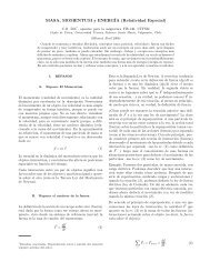
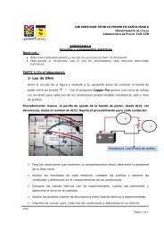
Figure 1. Experimental set up for Inverse<br />
Photoemission Spectroscopy. Photons are emitted<br />
after the interaction between electrons and the<br />
sample, only photons with 9.5 eV are <strong>de</strong>tected.<br />
References<br />
[1] S. Marchini, S. Günther, and J. Wintterlin,<br />
Phys. Rev. B 76, 075429 (2007).<br />
[2] T. Ohta, A. Bostwick, J. L. McChesney, T.<br />
Seyller, K. Horn and E. Rotenberg, PRL 98,<br />
206802 (2007).<br />
[3] P. W. Sutter, J. I. Flege and E. A. Sutter,<br />
Nature Materials, 7, 406-411 (2008).<br />
99 Valparaíso, Chile