

CV - Université de Rennes 1
CV - Université de Rennes 1
CV - Université de Rennes 1

Create successful ePaper yourself
Turn your PDF publications into a flip-book with our unique Google optimized e-Paper software.
Program<br />
Abstracts<br />
List of participants<br />
Accommodation and maps
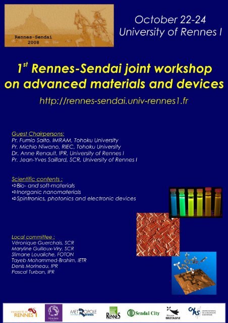
Program<br />
<strong>Rennes</strong>-Sendai Joint Workshop on Advanced Materials and Devices<br />
Tuesday 21 October Evening arrival and transfer to hotel<br />
Wednesday 22 October 8:15 – 8:45 Transfer from hotel<br />
8:45 - 9:00 Welcome and introduction meeting<br />
(D. Morineau / M. Niwano)<br />
9:00 – 9:20 Presentation of RIEC and IMRAM<br />
9:20 - 10:50 Bio-Soft Session (1/2)<br />
10:50 - 11:20 Coffee & tea break<br />
11:20 - 12:50 Bio-Soft Session (2/2)<br />
13:00 – 14:00 Lunch<br />
14 :30 - 16 :30 Labs visits<br />
16 :30 - 17 :00 Coffee<br />
17 :00 Transport to hotel<br />
19 :30 Diner organized by the Presi<strong>de</strong>nt of<br />
the University<br />
Thursday 23 October 9:00 – 9:40 Inorg Session<br />
9:40 – 10:50 Spin Session (1/2)<br />
10:50 – 11 :20 Coffee & tea break<br />
11:20 – 12:50 Spin Session (2/2)<br />
13:00 - 14:00 Lunch<br />
14 :30 - 16 :30<br />
Poster session<br />
Open discussion<br />
or visit of <strong>Rennes</strong> Atalante<br />
Technopark<br />
16 :30 - 17 :00 Coffee<br />
17 :00 Transport to hotel<br />
19 :30 Diner organized by <strong>Rennes</strong> Metropole<br />
Friday 24 October 9:30 – 17:00 Excursion to the Mont St Michel<br />
19:30 – 20:30 Reception at <strong>Rennes</strong> city hall<br />
Saturday 25 October Transport to the airport
Wednesday morning<br />
9:00 Intro-1 - Research Activities in the Research Institute of Electrical<br />
Communication (RIEC), Tohoku University<br />
Yôiti SUZUKI<br />
Deputy Director, Professor, RIEC, Tohoku University<br />
9:10 Intro-2 - Research Activities in the Institute of Multidisciplinary Research for<br />
Advanced Materials (IMRAM), Tohoku University<br />
Tokuji MIYASHITA<br />
Deputy Director, Professor, IMRAM, Tohoku University<br />
- Bio and soft matter:<br />
9:20 BioSoft-1 - Fabrication of Plasmonic Nanosheets and their Bioapplication<br />
Kaoru Tamada<br />
Research Institute of Electrical Communication, Tohoku University<br />
9:38 BioSoft-2 - Detection of proteins by SGFET: technology, functionnalization and<br />
transferrin quantification<br />
F. LeBihan 1 , T. Mohammed-Brahim, A. Girard, O. De Sagazan, F. Geneste 2 , S.<br />
Dauphas, A. Corlu, P. Brissot, O. Loréal, C. Guillouzo, L. Guéné, A. Le Treut, M.<br />
Trancart, and C. Chesné<br />
1 Institut d’Electronique et <strong>de</strong>s Télécommunications <strong>Rennes</strong>, UMR CNRS 6164, University of <strong>Rennes</strong> 1<br />
2 Sciences Chimiques <strong>de</strong> <strong>Rennes</strong>, UMR CNRS 6226, University of <strong>Rennes</strong> 1<br />
9:52 BioSoft-3 - In situ real-time monitoring of biomolecular interactions by using<br />
surface infrared spectroscopy<br />
Ayumi Hirano-Iwata, Ryo-taro Yamaguchi, Ko-ichiro Miyamoto, Yasuo Kimura,<br />
and Michio Niwano<br />
Laboratory for Nanoelectronics and Spintronics, Research Institute of Electrical Communication,<br />
Tohoku University<br />
10:14 BioSoft-4 - NanoBio and Chemical Biology / Tailor Ma<strong>de</strong> Biopolymers<br />
- Pepti<strong>de</strong> Ribonucleic Acids (PRNAs): Novel Strategy for Active Control of RNA<br />
Recognition by External Factors & Supramolecular Asymmetric<br />
Photochirogenesis with Biopolymers<br />
Takehiko Wada<br />
Institute of Multidisciplinary Research for Advanced Materials, Tohoku University<br />
10:32 BioSoft-5 - A Scaffold of biological molecules to manufacture monodisperse<br />
silica nanotubes<br />
Emilie Pouget, Christophe Tarabout, Erik Dujardin, Annie Cavalier, Céline Valery,<br />
Maité Paternostre, Valérie Marchi-Artzner, and Franck Artzner<br />
Institut of Physics of <strong>Rennes</strong>, CNRS-University of <strong>Rennes</strong> 1
10:50 - 11:20 - Coffee and tea break -<br />
11:20 BioSoft-6 Inelastic tunneling spectroscopy of C8 alkanethiol self assembled<br />
monolayer using scanning tunneling microscopy at 4.3 K<br />
Tadahiro Komeda<br />
Institute of Multidisciplinary Research for Advanced Materials, Tohoku University<br />
11:38 BioSoft-7 - Structuring of Liquids at the Solid-Liquid Interface<br />
Kazue Kurihara<br />
Institute of Multidisciplinary Research for Advanced Materials, Tohoku University<br />
11:56 BioSoft-8 - Dynamics of soft matter and complex fluids in confined<br />
geometry<br />
D. Morineau, R. Lefort, R. Busselez, Q. Ji, R. Guégan, G. Chahine, M.<br />
Guendouz, P. Huber, J.-M. Zanotti, and B. Frick<br />
Institute of Physics of <strong>Rennes</strong>, CNRS-University of <strong>Rennes</strong> 1, <strong>Rennes</strong> France<br />
12:14 BioSoft-9 Organic Nano-Electronics based on Polymer Nano-sheet Assemblies<br />
Tokuji Miyashita<br />
Institute of Multidisciplinary Research for Advanced Materials, Tohoku University<br />
12:32 BioSoft-10 In-situ redox carboxylate generation to <strong>de</strong>sign homo- and heterometallic<br />
complexes<br />
Olivier Cador, Konstantin S. Gavrilenko, Stéphane Golhen, Vitaly V. Pavlishchuk, and<br />
Lahcène Ouahab<br />
Sciences Chimiques <strong>de</strong> <strong>Rennes</strong>, UMR CNRS 6226, University of <strong>Rennes</strong> 1
- Inorganic materials:<br />
Thursday morning<br />
9:00 Inorg-1 - Scanning nonlinear dielectric microscopy with atomic resolution<br />
Yasuo Cho, Shin-ichiro Kobayashi and Ryusuke Hirose<br />
Research Institute of Electrical Communication, Tohoku University<br />
9:18 Inorg-2 - Novel Functional Surfaces, Nanoparticles and Nanomaterials Based on<br />
Metal Atom Clusters<br />
S. Cordier, F. Dorson, F. Grasset, Y. Molard, B. Fabre, S. Ababou-Girard, C. Perrin<br />
Sciences Chimiques <strong>de</strong> <strong>Rennes</strong>, UMR CNRS 6226, University of <strong>Rennes</strong> 1<br />
9:36 Inorg-3 - Characterization of Microscopic Chemical State and Composition of<br />
Complex Metal Oxi<strong>de</strong>s<br />
Shigeru Suzuki and Kozo Shinoda<br />
Institute of Multidisciplinary Research for Advanced Materials, Tohoku University<br />
9:54 Inorg-4 - Control of Composition and Structure of KTaxNb1-xO3 Ferroelectric<br />
Oxi<strong>de</strong> Thin Films<br />
Maryline Guilloux-Viry, Wei Peng, Quentin Simon, Stéphanie Députier, Valérie<br />
Bouquet, André Perrin<br />
Sciences Chimiques <strong>de</strong> <strong>Rennes</strong>, UMR CNRS 6226, University of <strong>Rennes</strong> 1<br />
-Spintronics, photonics and electronic <strong>de</strong>vices<br />
10:12 Spin-1 - Magnetic Domain Wall Dynamics in (Ga,Mn)As<br />
Fumihiro MATSUKURA and Hi<strong>de</strong>o OHNO<br />
Laboratory for Nanoelectronics and Spintronics, Research Institute of Electrical Communication,<br />
Tohoku University<br />
10:30 Spin-2 - BEEM investigation of some spintronics heterostructures<br />
P. Turban, S. Guézo, C. Lallaizon, P. Schieffer, B. Lépine, G. Jézéquel<br />
Institut of Physics of <strong>Rennes</strong>, CNRS-University of <strong>Rennes</strong> 1<br />
10:50 – 11:20 - Coffee and tea break -
11:20 Spin-3 -Transmission Electron Microscopy of Advanced Materials<br />
Daisuke SHINDO<br />
Institute of Multidisciplinary Research for Advanced Materials, Tohoku University<br />
11:38 Spin-4 - Carbon-rich Molecular Architectures with Redox-switchable Non-linear<br />
Optical Properties. From Organometallic Molecules to Organometallic Materials<br />
Nicolas Gauthier, Frédéric Paul, Gilles Argouarch, Isabelle Ledoux, Mark Humphrey,<br />
Marek Samoc, Malgorzata Makowska-Janusik, Ivan V. Kityk and B. Fabre<br />
Sciences Chimiques <strong>de</strong> <strong>Rennes</strong>, UMR CNRS 6226, University of <strong>Rennes</strong> 1<br />
11:56 Spin-5 - Growth of InAs/InP Nanostructures for Optical Telecomunication<br />
Devices.<br />
Olivier Dehaese<br />
FOTON, UMR CNRS 6082 – INSA <strong>de</strong> <strong>Rennes</strong><br />
12:14 Spin-6 - InP-Based High Electron Mobility Transistors for Millimeter-Wave<br />
Applications and Plasmon-Resonant Devices<br />
Tetsuya Suemitsu<br />
Research Institute of Electrical Communication (RIEC), Tohoku University<br />
12:32 Spin-7 - Millimeter-wave antennas and Metamaterials<br />
Ronan Sauleau<br />
Institut d’Electronique et <strong>de</strong>s Télécommunications <strong>Rennes</strong>, UMR CNRS 6164, University of <strong>Rennes</strong> 1
Research Activities in the Research Institute of Electrical Communication (RIEC),<br />
Tohoku University<br />
SUZUKI Yôiti<br />
Deputy Director, Professor, RIEC, Tohoku University<br />
Research institutes affiliated with Japanese national universities are organizationally<br />
equivalent to faculties and graduate schools. The main difference between research<br />
institutes and faculties and graduate schools is that the main mission of research institutes is<br />
to conduct advanced research.<br />
Tohoku University was foun<strong>de</strong>d in 1907 as Tohoku Imperial University: the third national<br />
university in Japan after those in Tokyo and Kyoto. The Research Institute of Electrical<br />
Communication (RIEC) was established in 1935 as a research institute affiliated with<br />
Tohoku Imperial University. At that time, in the Department of Electrical Engineering of<br />
Tohoku Imperial University, a growing ten<strong>de</strong>ncy towards research marked science and<br />
technology for electrical communication. Great efforts ma<strong>de</strong> in these fields produced<br />
pioneering studies such as those of the Yagi-Uda antenna and divi<strong>de</strong>d ano<strong>de</strong>-type<br />
magnetron, which were produced in the <strong>de</strong>partment in the late 1920s. Based on such<br />
prominent activities, RIEC was foun<strong>de</strong>d. In the seven <strong>de</strong>ca<strong>de</strong>s since its foundation, RIEC<br />
continues to excel as the only national-university-affiliated research institute addressing<br />
information and communication technology, with various research fields encompassing<br />
hardware and software. In 1994, our research institute was promoted as a National Center<br />
for Co-operative research, addressing “theory and applications of intelligent information<br />
science and communication theory”.<br />
At present, it comprises 4 research divisions consisting of 23 research groups and 3<br />
research facilities with 12 groups. The four research divisions are the following. The<br />
Information Devices Division carries out research into materials and <strong>de</strong>vices for<br />
communication technology. The Broadband Engineering Division specifically examines the<br />
<strong>de</strong>velopment of new technologies for the transmission and storage of vast quantities of data.<br />
The Human Information Systems Division conducts research into intelligent information<br />
processing. The Systems and Software Division is <strong>de</strong>veloping advanced system software<br />
for the new information society. The three research facilities emphasize examinations<br />
organized into short-, medium-, and long-term projects. The Research Center for 21st<br />
Century Information Technology was established in 2002 to realize short-term (typically for<br />
five years) collaboration between the Institute and industrial partners. The Center seeks to<br />
<strong>de</strong>velop information technology products using the advanced technologies and intellectual<br />
property <strong>de</strong>veloped at the Institute. For the medium term, the Laboratory for Nanoelectronics<br />
and Spintronics, housed in newly built facilities, is carrying out fundamental research into<br />
high-speed semiconductor <strong>de</strong>vices and advanced nano-spin science. Smaller and faster<br />
electronic <strong>de</strong>vices, non-volatile memories, and molecular and bio-information <strong>de</strong>vices are<br />
some expected fruits of this research. Meanwhile, the Laboratory for Brainware Systems is<br />
working towards its long-term goal of the seamless fusion of real and virtual worlds at the<br />
human-computer interface. The Institute and its members aim to continue its tradition of<br />
world-class research and innovation into this century.
Name: SUZUKI, Yôiti Dr.<br />
DATE of Birth: 11th, January, 1954<br />
CURRICULUM VITAE<br />
Educational Background:<br />
Dr. Engineering: March 1981, Tohoku University, Sendai, Electrical and<br />
Communication Engineering<br />
M. Engineering: March 1978, Tohoku University, Sendai, Electrical and<br />
Communication Engineering<br />
B. Engineering: March 1976, Tohoku University, Sendai, Electrical<br />
Engineering<br />
February 20, 2005<br />
Professional Experience:<br />
2008- Director, Information Synergy Organization, Tohoku University<br />
2007- Deputy Director, Research Institute of Electrical Communication, Tohoku University<br />
1999- Professor, Research Institute of Electrical Communication and Graduate School of<br />
Information Sciences, Tohoku University<br />
1995-1997 Guest Researcher, Toyoda Physical and Chemical Research Institute<br />
1994-1996 Guest Researcher, The National Institute of Special Education<br />
1991-1992 Guest Researcher, Institute for Human-machine Communication,<br />
Technical University of Munich<br />
1989- 1999 Associate Professor, Research Institute of Electrical Communication, Tohoku University<br />
1987-1989 Associate Professor, Computer Center, Tohoku University<br />
1981-1987 Research Associate, Research Institute of Electrical Communication, Tohoku University<br />
Research interests:<br />
Information processing in human auditory system, particularly on spatial hearing<br />
Development of precise three-dimensional virtual auditory displays<br />
Digital signal processing of sound signals (microphone array, digital watermarking)<br />
Development of future digital hearing aid algorithms including precise evaluation of speech<br />
intelligibility<br />
Human multimodal information processing consisting of hearing, vision and motion perception<br />
Environmental noise evaluation; evaluation of future risks on hearing by leisure activities (music as<br />
noise)<br />
Prizes<br />
Funai Best Paper Award, FIT2005, 2005<br />
The Sato Prize, the best paper award of the Acoustical Society of Japan, 1994<br />
The Sato Prize, the best paper award of the Acoustical Society of Japan, 1992<br />
The Awaya Prize (the best presentation award for young researchers), the Acoustical Society of Japan,<br />
1986<br />
Aca<strong>de</strong>mic Activities<br />
2007- Chairperson, Publication Committee. Acoustical Society of Japan<br />
2006- Member, Council Board, Virtual Reality Society of Japan<br />
2005-2007 Presi<strong>de</strong>nt, the Acoustical Society of Japan<br />
2004-2005 Chairperson, Committee for physio- and psycho-acouttics, Acoustical Society of Japan<br />
2003-2005 Chairperson, Editorial Board, Acoustical Society of Japan<br />
2002-2004 Chairperson, Committee for Technical Affairs, INCE/Japan<br />
2001-2003 Vice-presi<strong>de</strong>nt, the Acoustical Society of Japan<br />
2000-2004 Member, Board of Directors, INCE/Japan<br />
1995-2001 Member, Board of Directors of the Acoustical Society of Japan
Research fields and main publications SUZUKI, Yôiti Dr.<br />
SUZUKI, Yôiti is Professor, Acoustic Information Systems Laboratory in Human Information Systems<br />
Division, Research Institute of Electrical Communication, Tohoku University, Sendai, Japan. His<br />
standpoint is that human beings are regar<strong>de</strong>d as the extreme source and recipient of information in any<br />
communication systems. With this standpoint, he has been <strong>de</strong>voting into <strong>de</strong>veloping advanced acoustic<br />
communication systems based on good knowledge of human auditory system as well as multimodal<br />
perception relating to hearing. Several of his main archives are as follows:<br />
1. Hearing preception<br />
・ Futoshi Asano, Yôiti Suzuki, and Toshio Sone, “Role of spectral cues in median plane localization,”<br />
J. Acoust. Soc. Am., 88 (1990), 159-168.<br />
・ Noriaki Asemi, Yoichi Sugita, Yôiti Suzuki, “Auditory search asymmetry between pure tone and<br />
temporal fluctuating sounds distributed on the frontal-horizontal plane,” Acta Acustica united with<br />
Acustica, 89 (2) (2003), 346-354<br />
・ Yôiti Suzuki and Hisashi Takeshima, “Equal-loudness-level contours for pure tones,” J. Acoust. Soc.<br />
Amer., 116 (2) (2004), 918-933.<br />
2. Multimodal perception<br />
・ Yoichi Sugita and Yôiti Suzuki, “Implicit estimation of sound-arrival time,” Nature, 421, (2003),<br />
911-911<br />
・ Shuichi Sakamoto, Yusuke Osada, Yôiti Suzuki and Jiro Gyoba, “The effects of linearly moving<br />
sound images on self-motion perception,” Acoustical Science and Technology, 25 (1) (2004),<br />
100-102<br />
・ Koji Abe, Kenji Ozawa, Yôiti Suzuki and Toshio Sone,<br />
Comparison of the effects of verbal versus visual information about sound sources on the perception<br />
of environmental sounds, Acta Acustica united with Acustica, 92 (2006), 51-60.<br />
3. High-<strong>de</strong>finition auditory display<br />
・ Yukio Iwaya and Yôiti Suzuki: “Ren<strong>de</strong>ring Method of Moving Sound Source with the Doppler<br />
Effect in Sound Space,” Applied Acoustics, 68 (8), 976-922, 2007.<br />
・ Satoshi Yairi, Yukio Iwaya and Yo-iti Suzuki<br />
Development of virtual auditory display software responsive to head movement (in Japanese with<br />
English abstract), Trans. of the Virtual Reality Society of Japan, 11 (6) (2006) 437-446.<br />
4. Digital signal processing of sound signal<br />
・ Ryouichi Nishimura, Yôiti Suzuki and Byeong-Seob Ko: “Advanced Audio Watermarking Based on<br />
Echo Hiding: Time-Spread Echo Hiding,” Digital Audio Watermarking Techniques and<br />
Technologies, Information Science Reference, pp. 123-151, New York, USA, 2007<br />
・ Time-spread echo method for digital audio watermarking,<br />
IEEE Trans. on Multimedia, Vol. 7, No. 2, pp. 212-221, 2005.<br />
Byeong-Seob Ko, Ryouichi Nishimura and Yôiti Suzuki<br />
Other than the above, 126 papers in refereed journals as well as 146 presentations at international<br />
conferences, 17 tutorial papers, 15 book chapters, and 2 books.<br />
2
Fabrication of Plasmonic Nanosheets and their Bioapplication<br />
Kaoru Tamada<br />
1 Research Institute of Electrical Communication, Tohoku University, Sendai, Japan<br />
tamada@riec.tohoku.ac.jp<br />
The interdisciplinary field of research combining nanobiotechnology and information technology<br />
attracts our exceeding interests. These studies stand on the <strong>de</strong>velopment of new materials created by<br />
self-assembly of functional molecules and nanomaterials, leading to new classes of biosensing <strong>de</strong>vices.<br />
The plasmons, especially the combination of surface plasmons propagating along the metal-organic<br />
interface and local surface plasmons on metal nanoparticles is crucial to control and manipulate<br />
localized light in nano-scale for nano-sensing [1,2].<br />
In this paper, we present our latest result concerning the coupling between propagating surface<br />
plasmons on flat gold surface and local plasmons on silver nanoparticles [2]. The silver nanoparticles<br />
(core diameter: 4nm) are <strong>de</strong>posited on the substrate as “nano-sheet” composed of two dimensional<br />
crystalline layer fabricated at air-water interface, in which the distance between the particle cores is<br />
controlled accurately by the thickness of the shell layers. We found the silver nano-sheet <strong>de</strong>posited on<br />
the glass exhibits a significant shift of plasmon absorption band in UV–vis–Near-IR spectra to the<br />
longer wavelength (c.a. 50nm), while the peak width was rather reduced (sharpened) in the sheet<br />
formation. By use of this i<strong>de</strong>al two dimensional giant crystals composed of silver nanoparticles, we<br />
examined several fundamental issues concerning the propagating and the local surface plasmons and<br />
their coupling effect on the optical responses. This flexible, transferable nanosheet which can trap and<br />
transport bulk light efficiently is the promising building block for various types of plasmonic bio<strong>de</strong>vices.<br />
References<br />
[1] X. Li, K. Tamada, A. Baba A, W. Knoll, M. Hara, J. Phys. Chem. B, 2006, 110, 15755-15762.<br />
[2] K. Tamada, F. Nakamura, M. Ito, X.Li, A. Baba, Plasmonics, 2007, 2, 185-191.<br />
[3] C.D. Keum, N. Ishii, K. Michioka, P. Wulandari, K. Tamada, M. Furusawa, H. Fukushima, J. Nonlinear Opt.<br />
Phys. Mater. 2008, 17, 131-142.
Kaoru TAMADA<br />
Professor<br />
Research Institute of Electrical Communication<br />
Tohoku University<br />
2-1-1 Katahira, Aoba-ku, Sendai 980-8577, JAPAN<br />
TEL.+81-22-217-6100 / FAX.+81-22-217-6102<br />
Email: tamada@riec.tohoku.ac.jp<br />
http://www.tamada.riec.tohoku.ac.jp/in<strong>de</strong>x.html<br />
Education<br />
TOHOKU UNIVERSITY<br />
Research Institute of Electrical Communication<br />
2-1-1 Katahira,Aoba-ku, Sendai 980-8577, JAPAN<br />
B.S., Chemistry, 1984, Nara Women’s University, Japan<br />
Dr of Science, 1994, Nara Women’s University, Japan<br />
Thesis entitled: “Characterization of Inhomogeneous<br />
Monolayer Films on the Water Surface with FRAP and Capillary Wave technique”<br />
Professional Experiences<br />
1984-1991 Researcher, JSR Co. Ltd.<br />
1991-1993 Researcher, Dept of Chemistry, University of Wisconsin-Madison,USA<br />
1994-1995 Post-doc fellow, RIKEN Frontier International Program, Wako<br />
1995-2000 Senior Scientist, National Institute of Materials and Chemical Research, Tsukuba<br />
1997 Visiting Follow, Dept of Applied Mathematics, Australian National University,<br />
Australia<br />
1998-1999 Visiting Fellow, Max-Planck Institute for Polymer Research, Germany<br />
1999 Project Evaluation Office, Ministry of International Tra<strong>de</strong> and Industry, Tokyo<br />
2000-2005 Advisor, Spatio-Temporal Function Materials, RIKEN Frontier System, Wako<br />
2000-2007 Senior Scientist, National Institute of Advanced Industrial Science and<br />
Technology (AIST), Tsukuba<br />
2001 –2004 Visiting Senior Fellow, National University of Singapore (NUS), Singapore<br />
2005-2007 Associate professor, Department of Electronic Chemistry,<br />
Tokyo Institute of Technology (TITech), Yokohama<br />
2007-date Professor, Research Institute of Electrical Communication, Tohoku University,<br />
Sendai<br />
2006-date Adjunct Professor, Department of Physics, National University of<br />
Singapore(NUS), Singapore<br />
Professional Service Activities<br />
2008-date Vice Chair, Division of Molecular Electronics and Bioelectronics<br />
Japan Applied Physics Meeting<br />
2006-date Board member, The Surface Science Society of Japan<br />
2006-2011 Advisor, “Photons on Soft Materials”, PRESTO, JST basic Research Programs<br />
Field of Research<br />
Self-assembled Monolayers, Metal Nanoparticles, Surface Plasmons, Biosensors, Surface<br />
spectroscopy, Surface physical chemistry
TOHOKU UNIVERSITY<br />
Research Institute of Electrical Communication<br />
2-1-1 Katahira,Aoba-ku, Sendai 980-8577, JAPAN
Selection of recent publications<br />
TOHOKU UNIVERSITY<br />
Research Institute of Electrical Communication<br />
2-1-1 Katahira,Aoba-ku, Sendai 980-8577, JAPAN<br />
Reversible work function changes induced by photoisomerization of asymmetric azobenzene<br />
dithiol self-assembled monolayers on gold, L.F.N.A.Qune, H. Akiyama, T. Nagahiro, K. Tamada,<br />
A.T.S. Wee, Apply. Phys. Lett. 93, 083109 (2008).<br />
Coordination of carboxylate on metal nanoparticles characterized by Fourier transform<br />
infrared spectroscopy, P. Wulandari, T. Nagahiro, K. Michioka, K. Tamada, K. Ishibashi, Y.<br />
Kimura, M. Niwano, Chem. Lett. 37, 888-889 (2008).<br />
A Gram scale synthesis of monodispersed silver nanoparticles capped by carboxylate and their<br />
ligand exchange, C.-D. Keum, N. Ishii, K. Michioka, K. Tamada, M. Hara, M. Furusawa, H.<br />
Fukushima, J. Nonlinear Optical Physics & Materials 17, 131-142 (2008).<br />
SPR-based DNA <strong>de</strong>tection with metal nanoparticles, Tamada K, Nakamura F, Ito M, Li XH,<br />
Baba A, Plasmonics 2, 185-191 (2007).<br />
Enhancement of surface plasmon resonance signals by gold nanoparticles on high-<strong>de</strong>nsity DNA<br />
microarrays, Ito M, Nakamura F, Baba A, Tamada K, Ushijima H, Lau KHA , Manna A, Knoll<br />
W, J. Phys. Chem. C, 111, 11653-11662 (2007).<br />
Tuning of electrical characteristics in networked carbon nanotube field-effect transistors using<br />
thiolated molecules. Lee CW, Zhang K Tantang H Lohani A, Mhaisalkar SG, Li LJ*, Nagahiro<br />
T, Tamada K, Chen Y, Appl. Phys. Lett., 91, 103515 (2007).<br />
Quantitative friction map on surface composed of beta-cyclo<strong>de</strong>xtrin monolayer. Sadaie M,<br />
Nishikawa N, Kumashiro Y, Ikezawa Y, Kumagai Y , Makino K, Ohnishi S, Tamada K, Hara M,<br />
Jpn. J. Appl.Phys. PART 1, 46, 7838-7845 (2007).<br />
Estimation of dielectric function of biotin-capped gold nanoparticles via signal enhancement on<br />
surface plasmon resonance, Li X., Tamada,K., Baba A., Knoll W., Hara M.<br />
J. Phys. Chem. B 110, 15755-15762 (2006).<br />
Highly sensitive <strong>de</strong>tection of processes occurring insi<strong>de</strong> nanoporous anodic alumina templates:<br />
A wavegui<strong>de</strong> optical study, KHA Lau, LS Tan, K.Tamada, MS San<strong>de</strong>r, W. Knoll, J. Phys.<br />
Chem.B 108, 10812-10818 (2004).<br />
Cationic self-assembled monolayers composed of gemini-structured dithiol on gold: A new<br />
concept for molecular recognition with the distance between adsorption sites<br />
S. Yokokawa, K. Tamada, E. Ito, M. Hara, J. Phys. Chem. B. 107, 15, 3544-3551 (2003).<br />
Fabrication of TTF-TCNQ charge transfer complex SAMs : a comparison between coadsorption<br />
method and layer-by-layer adsorption method<br />
R. Yuge, A. Miyazaki, T. Enoki, K. Tamada, F. Nakamura, M. Hara, J. Phys. Chem. B 106, 6894<br />
(2002).
Detection of proteins by SGFET: technology, functionnalization and<br />
transferrin quantification<br />
F. LeBihan 1 , T. Mohammed-Brahim 1 , A. Girard 1 , O. De Sagazan 1 , F. Geneste 2 , S. Dauphas 2,3 , A.<br />
Corlu 3 , P. Brissot 3 , O. Loréal 3 , C. Guillouzo 3 , L. Guéné 4 , A. Le Treut 4 , M. Trancart 5 , C. Chesné 5<br />
1<br />
IETR UMR 6062, <strong>Université</strong> <strong>Rennes</strong> 1<br />
2<br />
Sciences Chimiques UMR6226 <strong>Université</strong> <strong>Rennes</strong> 1<br />
3<br />
INSERM, U522, CHU <strong>Rennes</strong><br />
4<br />
Lab. Biochimie Médicale, CHU <strong>Rennes</strong><br />
5<br />
Bioprédic International, <strong>Rennes</strong><br />
The aim of this study is to use a microsensor (SGFET) that <strong>de</strong>tects charges with high<br />
sensitivity and is <strong>de</strong>veloped at IETR, to achieve selective biosensors. This sensor is adapted for the<br />
<strong>de</strong>tection of specific proteins, here transferrin, for diagnosis and therapeutic applications in<br />
human health.<br />
This project is financed by the Agence Nationale <strong>de</strong> la Recherche (ANR DEPIST) and<br />
associates complementary skills with biologists, chemists, electronics specialists and clinicians.<br />
The sensing structure is a field effect transistor with a<br />
suspen<strong>de</strong>d gate. 1 Charge <strong>de</strong>tection is performed by electric<br />
measurements (shift of the transistor characteristics) induced by the<br />
immobilized biological species. This particular technology allows<br />
reaching high level of sensitivity 2 . Moreover, its small size should<br />
lead to the fabrication of a matrix sensor for the simultaneous<br />
<strong>de</strong>tection of different proteins and so to the achievement of a new<br />
type of lab-on-chip. The previously elaborated technology was improved to adapt the sensor to<br />
biological medium (complex medium with salts and proteins).<br />
The quantification of proteins is obtained by anchoring them in a selective manner.<br />
The selectivity of the sensor can be obtained by a good choice of sensitive layers <strong>de</strong>posited on<br />
the active surface (functionnalization), and by the use of antibodies allowing the specific<br />
binding with the target proteins. Preliminary measurements were performed using a<br />
glutaral<strong>de</strong>hy<strong>de</strong> linker. The results show the feasibility, but the reliability of the biosensor<br />
cannot be obtained without an efficient and reproducible functionnalization of the surface. A<br />
new functionalization 3 , <strong>de</strong>veloped by the chemistry team, was used. A stepwise<br />
functionnalization of silicon nitri<strong>de</strong> surfaces was achieved. The first step involves a<br />
silanization reaction leading to the formation of a silane film with a thickness estimated by<br />
XPS of one or two molecular layers. A monoprotected homobifunctionnalized linker is then<br />
grafted to avoid the formation of bridge structures on the surface. Deprotection of the ester<br />
groups of the immobilized linker and subsequent reaction with N-hydroxysuccinimid lead to<br />
N-hydroxysuccinimid activated surfaces able to react with biological species. The<br />
compatibility of the functionnalization procedure with the microsensor technology was<br />
checked. The <strong>de</strong>vice, the first results on functionnalization with electrical control, the<br />
selectivity after unspecific binding saturation and the range of transferrin <strong>de</strong>tection will be<br />
<strong>de</strong>scribed here.<br />
1<br />
T. Mohammed-Brahim, A.C. Salaun, F. Le Bihan, H. Kotb, F. Bendriaa, O. Bonnaud, Capteur pour la détection et/ou la<br />
mesure d’une concentration <strong>de</strong> charges contenues dans une ambiance, utilisation et procédé <strong>de</strong> fabrication correspondants<br />
French patent n° 0407583, july 2004.<br />
2<br />
F. Bendriaa, F. Le Bihan, A. Salaün, T. Mohammed-Brahim and O. Bonnaud, Study of mechanical maintain of suspen<strong>de</strong>d<br />
bridge <strong>de</strong>vices used as pH sensor, Journal of Non-Crystalline Solids, Volume 352, Issues 9-20, 15 June 2006, Pages 1246-<br />
1249.<br />
3<br />
S. Dauphas, A. Corlu, C. Guguen-Guillouzo, S. Ababou-Girard, O. Lavastre, F. Geneste, New Journal of Chemistry, 2008,<br />
32, 1228-1234.
Dr Florence Geneste (born 1969) CNRS fellow<br />
UMR-CNRS 6226, Equipe Catalyse et Organométalliques, <strong>Université</strong> <strong>de</strong> <strong>Rennes</strong> 1,<br />
Campus <strong>de</strong> Beaulieu, Bât. 10C, 35042 <strong>Rennes</strong> ce<strong>de</strong>x,<br />
Tel: 02 23 23 59 65, Fax: 02 23 23 59 67, e-mail: Florence.Geneste@univ-rennes1.fr<br />
Florence Geneste was graduated from the Ecole Supérieure <strong>de</strong> Chimie Physique<br />
Electronique <strong>de</strong> Lyon. She completed her Ph.D. in Chemistry at the University of Orsay<br />
un<strong>de</strong>r the supervision of Dr A. Moradpour on the synthesis of pentaradialenes, as a possible<br />
access to the total synthesis of C60. Following appointments as a postdoctoral researcher in<br />
Thomson-CSF (Orsay) with Dr P. Lebarny and at the University of Cambridge, with Prof. A.B. Holmes on the<br />
enhancement of electroluminescence in polymers, from molecules to materials, she joined the Catalysis and<br />
Organometallics group at the University of <strong>Rennes</strong>.<br />
Her research interest is primarily focused on the modification of carbon surfaces by electrochemical methods.<br />
She has particular interest in the covalent grafting of catalysts on graphite felt to provi<strong>de</strong> new materials for<br />
supported chemistry. She also <strong>de</strong>veloped flow analytical methods for the analysis of traces in solution. She is<br />
involved in several research projects on novel analytical methods for sensors and biosensors applications.<br />
Stu<strong>de</strong>nt supervising : 2 Ph.D. (100%), 1 post-doc (100%), 4 Master 2, 1 Ingénieur d’étu<strong>de</strong>s<br />
18 Master 1, Licence, IUT or BTS.<br />
Total number of publications: 29 and communications :23<br />
1- S. Dauphas, A. Corlu, C. Guguen-Guillouzo, S. Ababou-Girard, O. Lavastre, F. Geneste*,"Covalent Immobilization of Antibodies on<br />
Electrochemically Functionalized Carbon Surfaces.", New Journal of Chemistry, 2008, 32, 1228-1234.<br />
2- S. Dauphas, T. Delhaye, O. Lavastre, A. Corlu, C. Guguen-Guillouzo, S. Ababou-Girard, F. Geneste*, "Localization and Quantitative<br />
Analysis of Antigen-Antibody Binding on 2D Substrate Using Imaging NanoSIMS.", Analytical Chemistry, 2008, 80, 5958-5962.<br />
3- F. Geneste*, C. Moinet, Electrocatalytic oxidation of alcohols by a [Ru(tpy)(phen)(OH2 )] 2+ -modified electro<strong>de</strong>.", Journal of<br />
Electroanalytical Chemistry, 2006, 594, 105-110.<br />
4- F. Geneste*, C. Moinet, S. Ababou-Girard, F. Solal, "Stability of [RuII (tpy)(bpy)(OH2 )] 2+ -Modified Graphite Electro<strong>de</strong>s during Indirect<br />
Electrolyses.", Inorganic Chemistry, 2005, 44, 4366-4371.<br />
Dr France Le Bihan (born 1968) Maître <strong>de</strong> conférences<br />
Groupe Microélectronique, IETR, UMR 6164, <strong>Université</strong> <strong>de</strong> <strong>Rennes</strong>1<br />
Campus <strong>de</strong> Beaulieu, Bât. 11B, 35042 <strong>Rennes</strong> ce<strong>de</strong>x,<br />
Tel: 02 23 23 56 91, Fax: 02 23 23 56 57, e-mail: france.lebihan@univ-rennes1.fr<br />
Researcher in <strong>Rennes</strong> University at the IETR (Institut d'Electronique et <strong>de</strong><br />
Télécommunication <strong>de</strong> <strong>Rennes</strong>) since 1996. Research manager (HDR) since 2003. Involved in<br />
microtechnoloy and microsensors. Research activities first focused on the <strong>de</strong>velopment of<br />
magnetic sensors and conditioning circuits using polysilicon thin film technology and <strong>de</strong>vices. Main actual<br />
research in <strong>de</strong>velopment of charge sensors used as pH <strong>de</strong>tector and based on suspen<strong>de</strong>d gate transistors.<br />
Adaptation to biosensor and especially protein calibration. Also involved in integration of microfluidic systems<br />
with charge sensors matrix for the <strong>de</strong>velopment of new lab-on-chip. Supervisor of 3 Ph.D and 2 post-doc.<br />
Total number of publications: 22 and communications : 47, 1 patent<br />
1- T. Mohammed-Brahim, A.- C. Salaün, F. Le Bihan*, "SGFET as charge sensor : application to chemical and biological species<br />
<strong>de</strong>tection", Sensors & Transducers Journal, Vol. 90, Special Issue, April 2008, pp. 11-26.<br />
2- H. Mahfoz-Kotb, A.C. Salaün, F. Bendriaa, F. Le Bihan*, T. Mohammed-Brahim and J R Morante, "Sensing sensibility of surface<br />
micromachined Suspen<strong>de</strong>d Gate Polysilicon Thin Film Transistors", Sensors and Actuators B, Volume 118, Issues 1-2, 25 October<br />
2006, Pages 243-248.<br />
3- F. Bendriaa, F. Le Bihan*, A. Salaün, T. Mohammed-Brahim and O. Bonnaud, "Study of mechanical maintain of suspen<strong>de</strong>d bridge<br />
<strong>de</strong>vices used as pH sensor", Journal of Non-Crystalline Solids, Volume 352, Issues 9-20, 15 June 2006, Pages 1246-1249.<br />
4- T. Mohammed-Brahim, A.C. Salaun, F. Le Bihan*, H. Kotb, F. Bendriaa, O. Bonnaud, "Capteur pour la détection et/ou la mesure d’une<br />
concentration <strong>de</strong> charges contenues dans une ambiance, utilisation et procédé <strong>de</strong> fabrication correspondants", french patent n° 0407583 july<br />
2004.
Nano-Molecular Devices<br />
Fabrication of electronic <strong>de</strong>vices from functional<br />
molecules and nanostructures<br />
Staff:<br />
Michio NIWANO, Professor<br />
Ayumi IWATA-HIRANO, Associate Professor<br />
(Graduate School of Medical Engineering)<br />
Yasuo KIMURA, Assistant Professor<br />
Ken-ichi ISHIBASHI, Assistant Professor<br />
Research activities:<br />
The continuously increasing amount of data to be stored and manipulated<br />
is strong impetus in the search for molecular electronic <strong>de</strong>vices that are<br />
fabricated from various molecules with unusual electrical and optical<br />
properties. The use of supramolecules such as C60, organic metals and<br />
semiconductors, and biomolecules such as DNA will open entirely new<br />
horizons in the field of molecular <strong>de</strong>vice technology. The need to manipulate<br />
large amounts of genetic data requires the <strong>de</strong>velopment of new types of<br />
bio-information <strong>de</strong>vices, which may be constructed by combining molecular<br />
<strong>de</strong>vice technology with biotechnology.<br />
In accordance with these requirements, we are now searching for new<br />
types of molecular materials to be used in molecular <strong>de</strong>vices, while<br />
simultaneously trying to produce new types of molecular chemistry with the<br />
enormous existing infrastructure in silicon technology. Our goal is the<br />
realization of molecule-sized electronic <strong>de</strong>vices that enable signal generation,<br />
processing, transfer, amplification and more on the molecular scale.<br />
Research topics:<br />
1. Analysis of biological functions at semiconductor surfaces Development<br />
of bio-sensing systems<br />
2. Flexible organic electronic <strong>de</strong>vices using organic semiconductors and<br />
supramoleules<br />
3. Nano-scale characterization and control of surfaces and interfaces of<br />
organic <strong>de</strong>vices<br />
4. Fabrication of dye-sensitized solar cells<br />
Prof. Michio Niwano received Ph.D. <strong>de</strong>gree in nuclear physics from<br />
Tohoku University, Japan, in 1980. He was with the Faculty of Edication,<br />
Miyagi University of Education, Japan as an assistant researcher. He moved<br />
to Tohoku University in 1987. Since 1998, he has been a professor at the<br />
Research Institute of Electrical Communication (RIEC), Tohoku University,<br />
Japan. His research interest inclu<strong>de</strong>s nanoelectronics, bio-electronics and<br />
organic electronics. He is a member of ECS, MRS, and JSAP.<br />
HIRANO NIWANO KIMURA<br />
Organic single crystal of rubrene and a<br />
polymer organic semiconductor FET on a<br />
transparent substrate.<br />
Apoptosis (programmed cell <strong>de</strong>ath) of<br />
cells and infrared spectroscopy for the<br />
analysis of cell functions.<br />
TiO2 nanotubes fabricated by the<br />
electrochemical method (application to<br />
dye-sensitized solar cells).<br />
Papers:<br />
[1] Ken-ichi Ishibashi, Ryo-taro Yamaguchi, Yasuo Kimura, and Michio Niwano, “Fabrication of titanium<br />
oxi<strong>de</strong> nanotubes by rapid and homogeneous anodization in a mixture of perchloric acid and ethanol”, J.<br />
Electrochem. Soc., 155(1), K10-14 (2008).<br />
[2] Ryo-taro Yamaguchi, Ko-ichiro Miyamoto, Ken-ichi Ishibashi, Ayumi Hirano, Suhana Mohd Said, Yasuo<br />
Kimura, and Michio Niwano “DNA hybridization <strong>de</strong>tection by porous silicon-based DNA microarray in<br />
conjugation with infrared microspectroscopy” J. Appl. Phys., 102, 014303-1-7 (2007).<br />
[3] Ryo-taro Yamaguchi, Ayumi Hirano-Iwata, Yasuo Kimura, Ko-ichiro Miyamoto, Hiroko Isoda, Hitoshi<br />
Miyazaki, and Michio Niwano “Real time monitoring of cell <strong>de</strong>ath by surface infrared spectroscopy” Appl.<br />
Phys. Lett., 91, 203902-1- 203902-3 (2007).
In situ real-time monitoring of biomolecular interactions by using surface<br />
infrared spectroscopy<br />
Ayumi Hirano-Iwata, 1 Ryo-taro Yamaguchi, 1 Ko-ichiro Miyamoto, 2 Yasuo Kimura, 1<br />
and Michio Niwano 1<br />
1<br />
Laboratory for Nanoelectronics and Spintronics, Research Institute of Electrical<br />
Communication, Tohoku University, 2-1-1 Katahira, Aoba-ku, Sendai, Miyagi 980-8577,Japan<br />
2<br />
Department of Electronic Engineering, Graduate School of Engineering, Tohoku<br />
University, 6-6-05 Aza-Aoba, Aramaki, Aoba-ku, Sendai, Miyagi 980-8579, Japan<br />
Email: niwano@riec.tohoku.ac.jp<br />
Detecting biomolecular interactions is often the most critical step not only for biosensor and<br />
biochip applications but also for un<strong>de</strong>rstanding the un<strong>de</strong>rlying mechanisms of their actions. The<br />
most common approach for <strong>de</strong>tecting their binding relies on labeling of proteins with<br />
fluorescence, radioisotopes or enzymes to achieve highly sensitive <strong>de</strong>tection. However, labeling<br />
may affect their biological activities, especially for the small proteins or pepti<strong>de</strong>s. On the other<br />
hand, non-label <strong>de</strong>tection of the binding events based on the structural and conformational<br />
changes is another useful approach, because this approach does not perturb the biological<br />
activities of the target molecules. Furthermore, such structural change is specific for the<br />
interactions, leading to more precise discrimination between specific and non-specific<br />
interactions, which is sometimes very difficult for the labeling approaches.<br />
Fourier-transform (FT) infrared spectroscopy (IRAS) is a powerful tool for non-label<br />
<strong>de</strong>tection of structural changes induced by biomolecular interactions. IRAS has several<br />
advantages such as rapidity, easiness and applicability to various environments including crystals,<br />
aqueous solutions and optically turbid conditions like cell culture media. In addition, IRAS has<br />
potential to provi<strong>de</strong> information on multiple target molecules, which is particularly useful when<br />
we are monitoring dynamic and complex biomolecular systems. IRAS in the multiple internal<br />
reflection (MIR) geometry provi<strong>de</strong>s an i<strong>de</strong>al optical configuration to combine highly sensitive<br />
<strong>de</strong>tection and aqueoussolution phase measurements. By using MIR-IRAS we have recently<br />
succee<strong>de</strong>d in <strong>de</strong>tecting antigen-antibody interaction in aqueous solution without using high<br />
sample concentrations.<br />
We focuses on our MIR-IRAS approaches for label-free <strong>de</strong>tection and characterization of<br />
biomolecular interactions, such as DNA hybridization, DNA hydration, protein-protein<br />
interaction, cell growth and cell <strong>de</strong>ath. These biomolecular interactions were monitored both in<br />
D2O and H2O media. We <strong>de</strong>monstrate the utility of MIR-IRAS as an in situ monitoring both for<br />
analysis of biomolecular interactions and for the sensitive <strong>de</strong>tection of target biomolecules and<br />
their interactions.
Institute of Multidisciplinary Research for Advanced Materials (IMRAM)<br />
Tohoku University<br />
2-1-1 Katahira, Aoba-ku, Sendai 980-8577, Japan<br />
NanoBio and Chemical Biology / Tailor Ma<strong>de</strong> Biopolymers<br />
- Pepti<strong>de</strong> Ribonucleic Acids (PRNAs): Novel Strategy for Active Control of RNA Recognition by<br />
External Factors & Supramolecular Asymmetric Photochirogenesis with Biopolymers -<br />
Takehiko WADA<br />
Institute of Multidisciplinary Research for Advanced Materials (IMRAM), Tohoku University<br />
2-1-1 Katahira, Aoba-ku, Sendai 980-8577, JAPAN<br />
E-mail: hiko@tagen.tohoku.ac.jp<br />
A chemical synthesis and modification of DNA/RNA is the fundamental technology that has led the<br />
molecular biology revolution. Hence, a chemistry of DNA and RNA not only in vitro but also in vivo<br />
expects to open new generational stage of bioorganic chemistry and molecular biology, then the nucleic<br />
acids chemistry has received much attention in post-genome project era. Thus, focusing our research<br />
interest mostly on the recognition and complexation behavior control of biopolymers, such as DNA/RNA,<br />
proteins by external factors, toward the active control of cellular functions.<br />
Another topics are reaction control based on molecular recognition phenomena in both ground and<br />
electronically excited states; we are pursuing mechanistic and synthetic studies on asymmetric<br />
photochemistry with supramolecular biopolymers as chiral reaction fields.<br />
Current Research Projects are:<br />
1. Development of external stimuli responsible artificial nucleic acids<br />
2. Development of cancer cell specific gene therapy drugs, such as siRNA and/or antisense RNA strategy<br />
3. Creation of cellular signals responsible intelligent functional biomaterials<br />
4. New photochemical paradigm and methods for the study of chemical biology<br />
5. Creation of external stimuli responsible artificial enzymes and proteins<br />
6. Supramolecular asymmetric photochirogenesis with biopolymers and biomolecules as chiral nano<br />
reaction field/reactor<br />
Human Serum Albumin as a Chiral Nanoreactor<br />
HP: http://www.tagen.tohoku.ac.jp/labo/wada/in<strong>de</strong>x-j.html<br />
Ref. (Selected): J. Am. Chem. Soc., 130, 7526 (2008); J. Am. Chem. Soc., 129, 3478 (2007);<br />
J. Org. Chem., 72, 2707 (2007) (Cover picture); Chem.–Eur. J. 13, 2429 (2007) (Cover picture);<br />
J. Am. Chem. Soc., 126, 6568 (2004); J. Am. Chem. Soc. 125, 7492 (2003); J. Am. Chem. Soc., 125, 3008 (2003);<br />
J. Am. Chem. Soc., 124, 6942 (2002); J. Am. Chem. Soc., 122, 6900 (2000); J. Am. Chem. Soc., 122, 406 (2000);<br />
J. Am. Chem. Soc., 121, 8486 (1999); J. Am. Chem. Soc., 120, 10687 (1998). etc.
A SCAFFOLD OF BIOLOGICAL MOLECULES<br />
TO MANUFACTURE<br />
MONODISPERSE SILICA NANOTUBES<br />
Emilie POUGET 1 , Christophe TARABOUT, Erik DUJARDIN 2 ,<br />
Annie CAVALIER 1 , Céline VALERY 3 , Maité PATERNOSTRE 3 ,<br />
Valérie MARCHI-ARTZNER 4 , Franck ARTZNER 1<br />
1 Biomimetic Self Assemblies – IPR CNRS- <strong>Université</strong> <strong>Rennes</strong>1, FRANCE<br />
2 Groupe Nanosciences - CEMES / CNRS UPR 8011 – Toulouse, FRANCE<br />
3 SBFM - URA 2096 CEA/CNRS - CEA-Saclay, FRANCE<br />
4 UMR CNRS 6226 <strong>Université</strong> <strong>Rennes</strong> 1, France<br />
Nature is an unlimited source of inspiration for the <strong>de</strong>velopment of materials presenting<br />
original mechanical or optical properties . The current structural knowledge of some of these<br />
biological assemblies is promising as an inspiration source to try to mimics their<br />
supramolecular organizations. The <strong>de</strong>velopment of simplified system presenting properties<br />
close to biological assemblies is of great interest. To this end, there is still a long way in or<strong>de</strong>r<br />
to un<strong>de</strong>rstand not only the structures, but also their formation mechanisms.<br />
Lanreoti<strong>de</strong> molecules self-assemble in water into highly monodisperse<br />
supramolecular nanotubes, the diameter and wall thickness of which are 244Å and 18Å<br />
respectively. [1] Following biomineralization principles, we show that the self-assembled<br />
nanotubes can be used as a template to produce micron-long, bilayered silica nanotubes<br />
having a monodisperse diameter of 29 nm. The nanotubes organize spontaneously into<br />
centimeter-size, highly or<strong>de</strong>red bundles. Furthermore, the formation mechanism was<br />
elucidated using a range of techniques, including X ray diffraction, optical and electron<br />
microscopy [2].<br />
Fig.1. TEM micrograph of Lanreoti<strong>de</strong>/Silica fibers showing micro-long silica bilayered nanotubes.<br />
References:<br />
1] Biomimetic organization : octapepti<strong>de</strong> self assembly into nanotubes of viral capsid like dimension C. Valéry,<br />
M. Paternostre, B.Robert, T. Gulik-Krzywicki, T. Narayanan, J.-C. Dedieu, G. Keller, M.-L. Torres, R. Cherif-<br />
Cheikh, P. Calvo & F. Artzner Proc. Natl. Acad. Sci. USA, 2003,100(18), 10258-10262.<br />
2] Hierarchical architectures by synergy between dynamical template self-assembly and biomineralization, E.<br />
Pouget, E. Dujardin, A. Cavalier, A. Moreac, C. Valéry, V. Marchi-Artzner, T. Weiss, A. Renault, M.<br />
Paternostre, F. Artzner Nature Materials, 2007, 6, 434-439.
Franck ARTZNER<br />
Institut <strong>de</strong> physique <strong>de</strong> <strong>Rennes</strong><br />
<strong>Université</strong> <strong>Rennes</strong> 1<br />
263, avenue du Général Leclerc<br />
35042 <strong>Rennes</strong> ce<strong>de</strong>x, FRANCE<br />
PHONE : +33 (0)2 23 23 58 22 / FAX : +33 (0)2 23 23 67 17<br />
Email : franck.artzner@univ-rennes1.fr<br />
http://www.perso.univ-rennes1.fr/franck.artzner/<br />
Education<br />
Master of Science, 1994, Engineering School Ecole Supérieure <strong>de</strong> Physique et Chimie<br />
Industrielles , Paris<br />
Dr. of Science, 1997, University Paris XI<br />
Experience<br />
1997-1998 Post doc. at E22 in the group of J. Rädler ,TU München, GERMANY<br />
1999-2003 Permanent in the Pharmacy <strong>de</strong>partment, UMR CNRS 8612 <strong>Université</strong> Paris XI.<br />
2003- Biomimetic self-assemblies, IPR, <strong>Rennes</strong><br />
Experimental techniques<br />
+ Small Angle X-ray Scattering (SAXS) at Synchrotron Facilities and in house.<br />
+ Optical Microscopies Fluoresecnce, polarising, Dark Field<br />
+ Spectroscopies (FTIR, Raman)<br />
Field of Research<br />
Biomimetic Nanomaterials ma<strong>de</strong> self-assembly processes:<br />
- Peptidic Nanotubes<br />
- Silica Nanotubes<br />
- Protein Self Assemblies, actin<br />
- Synthetic Liquid Crystal, Surfactants, lipids,…<br />
- Biomineralisation<br />
- Composite phases with QDs, Quantum Dots<br />
Award<br />
2005 : Young Investigator Award of the Physical Chemistry Division of the French Chemical<br />
Society (SFC) and the French Physical Society (SFP)
Franck ARTZNER<br />
Selection of Recent Publication<br />
1] E. Pouget, E. Dujardin, A. Cavalier, A. Moreac, C. Valéry, V. Marchi-Artzner, T.<br />
Weiss, A. Renault, M. Paternostre, F. Artzner*, Hierarchical architectures by<br />
synergy between dynamical template self-assembly and biomineralization, Nature<br />
Materials, 2007, 6, 434-439.<br />
2] C. Valéry, M. Paternostre, B.Robert, T. Gulik-Krzywicki, T. Narayanan, J.-C.<br />
Dedieu, G. Keller, M.-L. Torres, R. Cherif-Cheikh, P. Calvo & F. Artzner*,<br />
Biomimetic organization : octapepti<strong>de</strong> self assembly into nanotubes of viral capsid<br />
like dimension, Proc. Natl. Acad. Sci. USA, 2003, 100(18), 10258-10262.<br />
3] A. Richard, V. Marchi-Artzner, M.-N. Lalloz, M.-J. Brienne, F. Artzner, T. Gulik-<br />
Krzywicki, M.-A. Gue<strong>de</strong>au-Bou<strong>de</strong>ville, J.-M. Lehn*, Fusogenic supramolecular<br />
systems of vesicles induced by metal ion binding to amphiphilic ligands , Proc. Natl.<br />
Acad. Sci. USA 2004, 101(43), 15279-15284.<br />
4] A. Brizard, C. Aimé, T. Labrot, I. Huc, F. Artzner, B. Desbat, R. Oda*,<br />
Morphological control of twisted to helical ribbons and tubules from complex non<br />
chiral gemini-tartrate, J. Am. Chem. Soc. 2007, 129(12), 3754-3762.<br />
5] A. Dif, E. Henry, F. Artzner, M. Baudy-Floc’h, M. Schmutz, M. Dahan, V. Marchi-<br />
Artzner*, Interaction between water-soluble peptidic CdSe/ZnS nanocrystals and<br />
vesicles: formation of hybrid vesicles and con<strong>de</strong>nsed lamellar phases, J. Am. Chem.<br />
Soc., 2008, 130(26); 8289-8296.<br />
6] R. Oda*, M. Laguerre, I. Huc, F. Artzner*,Structure of self-assembled chiral nanoribbons<br />
and nano-tubules revealed in the hydrated state, J. Am. Chem. Soc., in<br />
presse .<br />
7] F. Boulmedais, P. Bauchat, M. J. Brienne, I. Arnal, F. Artzner, T. Gacoin, M.<br />
Dahan, V. Marchi-Artzner*, Water-soluble pegylated Quantum Dots: from a<br />
composite hexagonal phase to isolated micelles, Langmuir 2006, 22(23); 9797-<br />
9803.<br />
8] V. Roullier, F. Grasset, F. Boulmedais, F. Artzner, O. Cador, Valérie Marchi-<br />
Artzner*, Bioactivated Small PEG Hybrid Magnetic quantum dots Micelles Chem.<br />
Mater., in press.<br />
9] C.Valéry, F. Artzner*, A. Pandit, R. Cherif-Cheikh, I. Boisdé, E. Pouget, J.-M.<br />
Verbavatz, L. Bor<strong>de</strong>s and M. Paternostre*, Mutation approach for the un<strong>de</strong>rstanding<br />
of Lanreoti<strong>de</strong> self-assembly into nanotubes, Biophys. J., 2008, 94, 1782-1795.
Inelastic tunneling spectroscopy of C8 alkanethiol self assembled monolayer<br />
using scanning tunneling microscopy at 4.3 K<br />
IMRAM, Tohoku Univ., CREST-JST<br />
Tadahiro Komeda (komeda@tagen.tohoku.ac.jp)<br />
The <strong>de</strong>velopment of the minitualization technology enables to employ a single molecule for a <strong>de</strong>vice application.<br />
For example, intensive studies have been executed for the un<strong>de</strong>rstanding of electron transport through a single<br />
molecule that bridges two metal electro<strong>de</strong>s. The results have revealed intriguing electric phenomena, but the<br />
necessity of the characterization of molecules between electro<strong>de</strong>s has also been realized and it is mandatory to<br />
visualize and characterize an individual molecule. However, the use of TEM microscope is not favorable due to<br />
the damage to molecules. Scanning tunneling microscope (STM) has a big advantage for this purpose due to the<br />
low energy of injected electrons and small damage for molecules. STM can also be used to characterize and<br />
manipulate a single molecule. Inelastic tunneling spectroscopy (IETS) is one of the characterization techniques,<br />
which reveals the vibration features of molecules. Here, we report STM-IETS mesurement of C8 alkanethiole<br />
self assembled monolayer (SAM) at 4K. C8 SAM was prepared by immersing Au(111)/mica sample<br />
into hexane solution of C8 (1mM) for 6 min, and rinsed by ethanol just before inserted into a<br />
vacuum chamber for STM observation. The surface shows √3x√3 R30o or<strong>de</strong>red structure as shown in<br />
Fig.1 which is consistent with previous works. Figure 2 shows a comparison of I, dI/dV and d2I/dV2 obtained simultaneously at 4.3 K; the d2I/dV2 shows an excelent agreement with the previous work of<br />
Kushmerick et al using cross-wire method. Figure 3 corresponds to a high resolution SWTM-IETS spectrum<br />
with smaller modulation voltage for the bias voltage (Vrms=3.6 mV for modulation) of the C8 SAM. Feature of<br />
CH2 rocking (mark D, 88meV), CH3 rocking (E, 108meV) C-C streching (F, 130meV), and CH3 <strong>de</strong>formation (K,<br />
171meV) are highlighted and show a good consistency with the ones <strong>de</strong>tected with electron energy loss<br />
spectroscopy. This is the first <strong>de</strong>monstration that STM-IETS can reveal practically all the vibrational mo<strong>de</strong>s<br />
<strong>de</strong>tected with using EELS technique.[1]<br />
[1] N. Okabayashi, Y. Konda, and T. Komeda, Phys. Rev. Lett. 100, 217801 (2008).<br />
Fig.1 STM image of C 8<br />
alkanethiol SAM film at 4.3 K<br />
(a)<br />
(b)<br />
(c)<br />
Fig.2 Variation of I (a), dI/dV<br />
(b), d 2 I/dV 2 (c) STM-IETS on<br />
C8 alkanethiol molecule on the<br />
Au(111).<br />
Fig.3 High resolution STM-IETS<br />
obtained with V mod=3.6 mV. Spectra<br />
obtained for the regions of V sample>0<br />
and Vsample
(1) Original Paper - Publication lists (Recent five years)<br />
1. S. Katano, S. Ichihara, H. Ogasawara, H. S. Kato, T. Komeda, M. Kawai, and K. Domen, Adsorption structure of 1,3-butadiene on<br />
Pd(110), Surf. Sci. 502-503, 164 (2002).<br />
2. Y. Kim, T. Komeda, and M. Kawai, Single-molecule surface reaction by tunneling electrons, Surf. Sci. 502-503, 7 (2002).<br />
3. Yousoo Kim, Tadahiro Komeda and Maki Kawai, Single-Molecule Imaging and Repositioning of 1,3-Butadiene Adsorbed on Pd(110)<br />
Surface, Jpn. J. Appl. Phys. 41, 4924 (2002).<br />
4. T. Komeda, Y. Kim, and M. Kawai, Lateral motion of adsorbate induced by vibrational mo<strong>de</strong> excitation with inelastic tunneling<br />
electron, Surf. Sci. 502-503, 12 (2002).<br />
5. T. Komeda, Y. Kim, M. Kawai, B. N. J. Persson, and H. Ueba, Lateral hopping of molecules induced by excitation of internal<br />
vibration mo<strong>de</strong>, Science 295, 2055 (2002).<br />
6. T. Susaki, T. Komeda, and M. Kawai, Narrow photoemission peak at the Fermi level in Fe/Cu(111), Phys. Rev. Lett. 88, 187602<br />
(2002).<br />
7. Y. Kim, T. Komeda, and M. Kawai, Single-molecule reaction and characterization by vibrational excitation, Phys. Rev. Lett. 89,<br />
126104 (2002).<br />
8. S. Katano, Y. Kim, M. Furukawa, H. Ogasawara, T. Komeda, H.S. Kato, A. Nilsson, M. Kawai and K. Domen, Scanning Tunneling<br />
Microscopy and Near Edge X-ray Absorption Fine Structure Studies of Adsorption of Trans-2-butene on Pd(110), Jpn. J. Appl. Phys.<br />
41, 4911 (2002).<br />
9. Y. Kim, T. Komeda, and M. Kawai, Single-Molecule Imaging and Repositioning of 1,3-Butadiene Adsorbed on Pd(110) Surface, Jpn.<br />
J. Appl. Phys. 41, 4924 (2002).<br />
10. Y. Sainoo, Y. Kim, H. Fukidome, T. Komeda, M. Kawai, and H. Shigekawa, Characteristic Configuration of Cis-2-butene Molecule<br />
on Pd(110) Determined by Scanning Tunneling Microscopy, Jpn. J. Appl. Phys. 41, 4976 (2002).<br />
11. T. Komeda, H. Fukidome, Y. Kim, M. Kawai, Y. Sainoo, H. Shigekawa, Scanning Tunneling Microscopy Study of Water Molecules<br />
on Pd(110) at Cryogenic Temperature, Jpn. J. Appl. Phys. 41, 4932 (2002).<br />
12. Y. Sainoo, Y. Kim, T. Komeda, M. Kawai, and H. Shigekawa, Observation of cis-2-butene molecule on Pd(110) by cryogenic STM: site<br />
<strong>de</strong>termination using tunneling-current-induced rotation, Jpn. J. Appl. Phys. 41, 4976 (2002).<br />
13. M. Furukawa, H. Fujisawa, S. Katano, H. Ogasawara, Y. Kim, T. Komeda, A. Nilsson, and M. Kawai, Geometrical characterization<br />
of pyrimidine base molecules adsorbed on Cu(110) surfaces: XPS and NEXAFS studies, Surf. Sci. 532, 261 (2003).<br />
14. Y. Sainoo, Y. Kim, T. Komeda, M. Kawai, and H. Shigekawa, Observation of cis-2-butene molecule on Pd(110) by cryogenic STM: site<br />
<strong>de</strong>termination using tunneling-current-induced rotation, Surf. Sci. 536, L403 (2003).<br />
15. T. Komeda, Y. Kim, Y. Fujita, Y. Sainoo, and M. Kawai, Local chemical reaction of benzene on Cu(110) via STM-induced excitation, J.<br />
Chem. Phys. 120, 5347 (2004).<br />
16. M. Kawai, T. Komeda, Y. Kim, Y. Sainoo, and S. KatanoSingle-molecule reactions and spectroscopy via vibrational excitation. Phil.<br />
Trans. R. Soc. Lond. A 362, 1163-1171 (2004).<br />
17. Y. Sainoo , Y. Kim, T. Komeda, M. Kawai. Inelastic tunneling spectroscopy using scanning tunneling microscopy on trans-2-butene<br />
molecule: Spectroscopy and mapping of vibrational feature. J. Chem. Phys. 120, 7249 (2004).<br />
18. T. Takaoka, M. Inamura, S. Yanagimachi, I. Kusunoki, T. Komeda, Ammonia adsorption on and diffusion into thin ice films grown on<br />
Pt(111), J. Chem. Phys. 121 (2004) 4331-4338.<br />
19. Y. Sainoo, Y. Kim, T. Okawa, T. Komeda, H. Shigekawa, M. Kawai, Excitation of molecular vibrational mo<strong>de</strong>s with inelastic scanning tunneling microscopy<br />
processes: Examination through action spectra of cis-2-butene on Pd(110), Phys. Rev. Lett. 246102-5, 95 (2005).<br />
20. T. Komeda, Chemical i<strong>de</strong>ntification and manipulation of molecules by vibrational excitation via inelastic tunneling process with scanning tunneling microscopy,<br />
Prog. Surf. Sci. 78 (2005) 41.<br />
21. T. Yamaguchi, T. Komeda, Observation of Or<strong>de</strong>red Arrays of Adsorbed Lysozyme by Scanning Tunneling Microscopy, Japanese Journal of Applied Physics<br />
45 (2006) 2349.<br />
22. M. Furuhashi, T. Komeda, Direct Observation of Molecular Orbital at Carbon Nanotube End Japanese Journal of Applied Physics 46 (2007) L161.<br />
23. M. Inamura, T. Takaoka, T. Komeda, Penetration of ammonia molecule into ice film; activation energy analysis using Xe molecular beam irradiation Surf. Sci.<br />
601 (2007) 1072-1078.<br />
24. T. Takaoka, T. Komeda, Collision-induced migration of CO on Pt(9 9 7) surface, Surf. Sci. 601 (2007) 1090-1100.<br />
25. N. Zhu, T. Osada, T. Komeda, Supramolecular assembly of biphenyl dicarboxylic acid on Au(111), Surf. Sci. 601 (2007) 1789-1794.<br />
26. Y.-F. Zhang, N. Zhu, T. Komeda, "Mn-Coordinated Stillbenedicarboxylic Ligand Supramolecule Regulated by the Herringbone<br />
Reconstruction of Au(111) , J. Phys. Chem. C 111 (2007) , 16946-16950.<br />
27. Y.-F. Zhang, N. Zhu, T. Komeda, Programming of a Mn-coordinated 4-4'-biphenyl dicarboxylic acid nanosystem on Au(1 1 1) and<br />
investigation of the non-covalent binding of C60 molecules, Surf. Sci. 602 (2008) 614-619.<br />
28. T. Takaoka, T. Komeda, Estimation of Friction of a Single Chemisorbed Molecule on a Surface Using Inci<strong>de</strong>nt Atoms, Phys. Rev.<br />
Lett. 100 (2008) 046104-046104.<br />
29. T. Osada, N. Zhu, Y. Zhang, T. Komeda, Molecule-Precision Cavity Formation in Molecular Layer Using Scanning Tunneling<br />
Microscope Lithography, J. Phys. Chem. C 112 (2008) 3835-3839.<br />
30. T. Komeda, Y. Manassen, Distribution of frequencies of a single precessing spin <strong>de</strong>tected by scanning tunneling microscope,<br />
Appl. Phys. Lett. 92 (2008) 212506.<br />
31. N. Okabayashi, Y. Konda, T. Komeda, Inelastic Electron Tunneling Spectroscopy of an Alkanethiol Self-Assembled Monolayer<br />
Using Scanning Tunneling Microscopy, Phys. Rev. Lett. 100 (2008) 217801.<br />
32. Y. Kakefuda, K. Narita, T. Komeda, S. Yoshimoto, S. Hasegawa, Synthesis and Conductance Measurement of Periodic<br />
Arrays of Gold Nanoparticles, Appl. Phys. Lett. (in press).<br />
33. M. Furuhashi, T. Komeda, Chiral vector <strong>de</strong>termination of carbon nanotubes by observation of interference patterns near<br />
the end cap, Phys. Rev. Lett. (in press)
Structuring of Liquids at the Solid-Liquid Interface<br />
Kazue Kurihara<br />
Institute of Multidisciplinary Research for Advanced Materials, Tohoku University<br />
Katahira, Aoba-ku, Sendai 980-8577, Japan, e-mail: kurihara@tagen.tohoku.ac.jp<br />
Liquid molecules, confined between nanometer scale space and at the solid-liquid interfaces,<br />
often exhibit quite different properties from those in the bulk. We have investigated the<br />
structuring of liquids at the solid-liquid interfaces employing new approaches based on surface<br />
forces measurement. Surface forces measurement, which directly measures molecular and<br />
surface interactions as a function of the surface separation, is a unique tool for surface<br />
characterization, enabling us to “monitor surface properties changing from the surface to the bulk<br />
(<strong>de</strong>pth profile)”. 1 This paper <strong>de</strong>scribes our recent researches including:<br />
Hydrogen bon<strong>de</strong>d molecular macroclusters on silica surface. 2-4 Liquid adsorption from<br />
binary liquids was investigated. Novel molecular architectures, macroclusters of alcohol,<br />
carboxylic acid or ami<strong>de</strong>, have been found on silica (glass and oxidized silicon) surfaces in<br />
non-polar solvents such as cyclohexane. Surface forces measurements revealed the long ranged<br />
attraction (e.g. extending to 30 ~ 40 nm for mono-alcohol), which associated with the macrocluster<br />
formation. FTIR-ATR spectroscopy has <strong>de</strong>monstrated that macroclusters are formed through<br />
hydrogen bonding between the surface silanol groups and adsorbed molecules and between<br />
adsorbed molecules. This phenomenon is used for preparing polymer nano-films by in-situ<br />
polymerization of precursor macroclusters on silica.<br />
Resonance shear measurement of confined<br />
liquids. 5-9 Resonance shear method has been <strong>de</strong>veloped<br />
in or<strong>de</strong>r to examine the or<strong>de</strong>ring behavior of liquid and<br />
liquid crystal molecules confined between two solid<br />
surfaces at the nanometer level. The frequency and the<br />
amplitu<strong>de</strong> of the resonance peak are highly sensitive to the<br />
long-range or<strong>de</strong>r of the confined molecules, affording the<br />
information about the viscosity, and lubrication and Figure. Resonance shear<br />
friction properties of confined liquids. The mechanism of<br />
measurement.<br />
nano-colloid viscosifiers has been also investigated.<br />
References:<br />
[1] K. Kurihara, in Nano-Surface Chemistry (M. Rosoff ed), Marcel Dekker Inc., 1-16 (2001).<br />
[2] M. Mizukami and K. Kurihara, Chemistry Letters, 1005-1006 (1999); 248-249 (2000).<br />
[3] M. Mizukami and K. Kurihara, J. Am. Chem. Soc., 124, 12889-12897 (2002).<br />
[4] M. Mizukami, G. Zhong, L. Zhang, I. Fukuchi, and K. Kurihara, Langmuir, 24, in press (2008).<br />
[5] C. D. Dushkin and K. Kurihara, Rev. Sci. Instrum., 69, 2095-2104 (1998).<br />
[6] K. Kurihara, Progr. Colloid Polymer Sci., 121, 49-56 (2002).<br />
[7] H. Sakuma, K.Ohtsuki and K. Kurihara, Phys. Rev. Lett., 96, 046104-046107 (2006).<br />
[8] Y. Kayano, H. Sakuma and K. Kurihara, Langmuir, 23, 8365-8370 (2007)<br />
[9] H. Kawai, H. Sakuma, M. Mizukami, T. Abe, Y .Fukao, H. Tajima and K. Kurihara, Rev. Sci.<br />
Instrum., 79, 043701-043701 (2008).
Dynamics of soft matter and complex fluids in confined<br />
geometry<br />
D. Morineau 1* , R. Lefort 1 , R. Busselez 1 , Q. Ji 1 , R. Guégan 2 , G. Chahine 1,3 , M.<br />
Guendouz 4 , J.-M. Zanotti 3 and B. Frick 5<br />
1 Institut <strong>de</strong> Physique <strong>de</strong> <strong>Rennes</strong>, CNRS-<strong>Université</strong> <strong>de</strong> <strong>Rennes</strong> 1, <strong>Rennes</strong> France<br />
2 Institut <strong>de</strong>s Sciences <strong>de</strong> la Terre, Orléans, France<br />
3 Laboratoire Léon Brillouin, CEA-Saclay, Gif-sur-Yvette, France<br />
4 Laboratoire d’Optronique, <strong>Université</strong> <strong>de</strong> <strong>Rennes</strong> 1, Lannion France<br />
5 Institut Laue-Langevin, Grenoble, France<br />
The manipulation of fluids in nanochannels has become a crucial issue for many foreseen<br />
applications in advanced nanomaterials and biotechnology. 1<br />
Fundamental questions arise from the unexpected behaviors of fluids confined in capillaries<br />
of nanometric dimension, which rule out the validity of some approaches <strong>de</strong>rived from the<br />
physics of liquids at the macro or microscopic scale.<br />
Intensive experimental studies of molecular liquids have shown that confinement on a<br />
nanometric scale consi<strong>de</strong>rably modifies the structure, phase behavior and molecular<br />
dynamics. Recently, much effort has focused on the unusual dynamic properties of lowmolecular<br />
weight liquids and glassforming systems in mesoporous solids. It reveals a<br />
complex entanglement of low dimensionality, finite size and surface effects. 2<br />
In this field, a current challenge is to extend the knowledge of nanoconfined liquids to more<br />
complex fluids such as soft matter or solutions of biological interest. The aim of the present<br />
contribution is in<strong>de</strong>ed to present some original features that are observed, when the confined<br />
system is tuned from pure globular liquids to anisotropic mesogenic molecules or multicomponent<br />
glassforming bioprotectant solutions. 3<br />
*http://perso.univ-rennes1.fr/<strong>de</strong>nis.morineau<br />
1 R. Busselez et al., Int. J. of Nanotechnology. 5, 867-884 (2008).<br />
2 See recent reviews : C. Alba-Simionesco et al., J. Phys.: Con<strong>de</strong>ns. Matter 18, R15 (2006); M.<br />
Alcoutlabi and G. B. McKenna, J. Phys.: Cond. Mat. 17, R461 (2005).<br />
3 R. Guégan et al., Phys. Rev. E 73 (1), 011707 (2006); R. Guégan et al., J. Chem. Phys. 126 (6),<br />
1064902 (2007); D. Morineau et al., ILL Annual Report Scientific Highlights (2007).
Institut <strong>de</strong> Physique <strong>de</strong> <strong>Rennes</strong><br />
<strong>Université</strong> <strong>Rennes</strong> I Umr 6251 CNRS<br />
Denis MORINEAU<br />
CNRS Researcher<br />
Institute of Physics of <strong>Rennes</strong> – UMR-CNRS 6251<br />
University of <strong>Rennes</strong> 1<br />
Tel. +33 (0)2 23 23 69 84<br />
Email : <strong>de</strong>nis.morineau@univ-rennes1.fr<br />
http://perso.univ-rennes1.fr/<strong>de</strong>nis.morineau<br />
Education<br />
2004 ‘Habilitation à Diriger <strong>de</strong>s Recherches’, University of <strong>Rennes</strong> 1<br />
“Glass transition and nanoconfined molecular fluids"<br />
1997 Ph. D in Physical-Chemistry, University of Paris XI, Orsay<br />
‘Structure of fragile glass-forming liquids by neutron scattering and molecular<br />
simulation”<br />
1992-96 Stu<strong>de</strong>nt of the ‘Ecole Normale Supérieure’, Paris<br />
Employment<br />
2002 - CNRS Researcher, Institute of Physics of <strong>Rennes</strong><br />
1997-2002 CNRS Researcher, Laboratory of Chemical Physics, University of Paris XI<br />
1998 NATO-NSF research fellow, Department of Chemistry, UCLA, Los Angeles<br />
1996-1997 Post-doc Fellow, Department of Biophysics, Ecole Polytechnique, Palaiseau<br />
Research administration<br />
2006 – 2009 Member of Scientific Council, Chairman of Sub-Committee<br />
Institute Laue Langevin (European neutron scattering facility) and LLB<br />
2005 - Member of the executive board of the Nanosciences Competence Center<br />
C’Nano North-West (www.cnanono.org)<br />
Fields of research – Expertises<br />
Chemical physics. Soft matter. Glassy dynamics in complex fluids. Nanoconfined phases.<br />
Nanofluidics. Neutron scattering. Molecular simulation.<br />
Institut <strong>de</strong> Physique <strong>de</strong> <strong>Rennes</strong><br />
Bât. 11A, <strong>Université</strong> <strong>Rennes</strong> 1 Tel : +33 2 23 23 69 84<br />
35042 <strong>Rennes</strong> Ce<strong>de</strong>x<br />
France<br />
Fax : +33 2 23 23 67 17<br />
e-mail : <strong>de</strong>nis.morineau@univ-rennes1.fr<br />
Website : perso.univ-rennes1.fr/<strong>de</strong>nis.morineau
Selection of publications<br />
Institut <strong>de</strong> Physique <strong>de</strong> <strong>Rennes</strong><br />
<strong>Université</strong> <strong>Rennes</strong> I Umr 6251 CNRS<br />
– ‘Finite-size and surface effects on the glass transition of liquid toluene confined in cylindrical<br />
mesopores’, D. MORINEAU, Y. XIA and C. ALBA-SIMIONESCO, J. Chem. Phys, 117, 8966-8972<br />
(2002).<br />
– ‘Liquids in confined geometry : How to connect changes in the structure factor to truly different<br />
structures’, D. MORINEAU and C. ALBA-SIMIONESCO, J. Chem. Phys., 118, 9389 (2003).<br />
– 'Confinement of molecular liquids : consequences on thermodynamic static and dynamical<br />
properties of benzene and toluene', C. ALBA-SIMIONESCO, E. DUMONT, B. FRICK, B. GEIL, D.<br />
MORINEAU, V. TEBOUL and Y. XIA, Eur. Phys. J. E, 12, 19-28 (2003).<br />
– ‘Structure of liquid and glassy methanol confined in cylindrical pores’, D. MORINEAU, R.<br />
GUEGAN, Y. XIA and C. ALBA-SIMIONESCO, J. Chem. Phys. 121, 1466-1473 (2004).<br />
– ‘Interfacial structure of an H-bonding liquid confined into silica nanopore with surface silanols’, R.<br />
GUEGAN, D. MORINEAU and C. ALBA-SIMIONESCO, Chem. Phys., 317, 236-244 (2005).<br />
– ‘Evi<strong>de</strong>nce of anisotropic quenched disor<strong>de</strong>r effects on a smectic liquid crystal confined in porous<br />
silicon.’, R. GUEGAN, D. MORINEAU, C. LOVERDO, W. BEZIEL and M. GUENDOUZ, Phys.<br />
Rev. E 73, 011707 (2006).<br />
– 'Phase Diagram and Glass Transition of Confined Benzene', Y. XIA, G. DOSSEH, D. MORINEAU<br />
and C. ALBA-SIMIONESCO, J. Phys. Chem. B 110, 19735 (2006)<br />
– « Molecular dynamics of a short range or<strong>de</strong>red smectic phase nanoconfined into porous silicon. »<br />
R. GUÉGAN, D. MORINEAU, R. LEFORT, A. MORÉAC, W. BÉZIEL, M. GUENDOUZ, J.-M.<br />
ZANOTTI, B. FRICK, J. Chem. Phys., 126, 064902 (2007)<br />
– ‘Incoherent Quasielastic Neutron Scattering Study of Molecular dynamics of 4-n-cyano-4’octylbiphenyl’,<br />
R. LEFORT, D. MORINEAU, R. GUÉGAN, C. ECOLIVET, M. GUENDOUZ, J.-M.<br />
ZANOTTI and B. FRICK, Physical Chemistry Chemical Physics, 10, 2993 – 2999 (2008)<br />
– 'Rich polymorphism of a rod−like liquid crystal (8CB) confined in two types of unidirectional<br />
nanopores' R. GUÉGAN, D. MORINEAU, R. LEFORT, W. BÉZIEL, M. GUENDOUZ, L. NOIREZ,<br />
A. HENSCHEL and P. HUBER, Eur. Phys. J. E, 26, 1292 (2008).<br />
– 'Continuous Paranematic-to-Nematic Or<strong>de</strong>ring Transitions of Liquid Crystals in Silica<br />
Nanochannels', A. V. KITYK, M. WOLFF, K. KNORR, D. MORINEAU, R. LEFORT and P.HUBER,<br />
Phys. Rev. Lett, (in press).<br />
– 'Relation between static short range or<strong>de</strong>r and dynamic heterogeneities in a nanoconfined liquid<br />
crystal',<br />
R. LEFORT, D. MORINEAU, R. GUEGAN, M. GUENDOUZ, J.-M. ZANOTTI and B. FRICK, Phys.<br />
Rev. E, Rapid Com., (in press).<br />
Institut <strong>de</strong> Physique <strong>de</strong> <strong>Rennes</strong><br />
Bât. 11A, <strong>Université</strong> <strong>Rennes</strong> 1 Tel : +33 2 23 23 69 84<br />
35042 <strong>Rennes</strong> Ce<strong>de</strong>x<br />
France<br />
Fax : +33 2 23 23 67 17<br />
e-mail : <strong>de</strong>nis.morineau@univ-rennes1.fr<br />
Website : perso.univ-rennes1.fr/<strong>de</strong>nis.morineau
Curriculum Vitae<br />
Name: Tokuji MIYASHITA<br />
Sex: Male<br />
Date of Birth: May 18th, 1948<br />
Affiliation:<br />
Institute of Multidisciplinary Research for Advanced<br />
Materials (IMRAM), Tohoku University<br />
Position: Professor, Deputy Director of IMRAM<br />
Distinguished Professor, Tohoku University<br />
Mailing address (business)<br />
Institute of Multidisciplinary Research for Advanced Materials, Tohoku University<br />
Katahira 2-1-1, Aoba-ku, Sendai 980-77, Japan<br />
TEL: +81-22-217-5637, Fax: +81-22-217-5642 e-mail: miya@tagen.tohoku.ac.jp<br />
URL address: http://res.tagen.tohoku.ac.jp/~profmiya/eng.html<br />
Education:<br />
BS, MS Department of Applied Chemistry, Tohoku University<br />
Ph.D. Tohoku University (1976)<br />
Experience:<br />
1985 Associate Professor, Faculty of Engineering, Tohoku University<br />
1993 Professor, Faculty of Engineering, Tohoku University<br />
2001 - Professor, Institute of Multidisciplinary Research for Advanced Materials,<br />
(IMRAM) Tohoku University<br />
2005 – Deputy Director IMRAM<br />
2008 – Distinguished Professor, Tohoku University<br />
Award<br />
� Award of The Society of Polymer Science, Japan (1997)<br />
� The prize of BCSJ in Chemical Society of JAPAN (2000)<br />
� Award of The Society of Pure & Applied Coordination Chemistry (2004).<br />
Aca<strong>de</strong>mic Activity<br />
2006-2007 Vice Presi<strong>de</strong>nt of The Society of Polymer Science Japan<br />
203-2004 The Editor-in-Chief, The Chemical Society of Japan<br />
Research Field and Interests:<br />
Polymer material chemistry, Molecular nanotechnology<br />
Soft Nano –<strong>de</strong>vices based on Polymer Nano-Assemblies and Architecture
In-situ redox carboxylate generation to <strong>de</strong>sign homo- and hetero-metallic<br />
complexes<br />
Olivier Cador, a Konstantin S. Gavrilenko, a,b Stéphane Golhen, a Vitaly V. Pavlishchuk, b<br />
Lahcène Ouahab a<br />
a Organométalliques et Matériaux Moléculaires, Sciences Chimiques <strong>de</strong> <strong>Rennes</strong>, UMR<br />
UR1-CNRS 6226, <strong>Université</strong> <strong>de</strong> <strong>Rennes</strong> 1, 263, Avenue du Général Leclerc, 35042 <strong>Rennes</strong><br />
Ce<strong>de</strong>x, France.<br />
b L. V. Pisarzhevskii Institute of Physical Chemistry of the National Aca<strong>de</strong>my of Sciences of the<br />
Ukraine, prospekt Nauki 31, 03028 Kiev, Ukraine.<br />
E-mail: olivier.cador@univ-rennes1.fr<br />
The <strong>de</strong>sign of molecular materials which exhibit specific electronic properties is<br />
becoming one the main issue of contemporary research. As a result, molecular magnetism has<br />
attracted much attention in the last two <strong>de</strong>ca<strong>de</strong>s because molecular-based magnetic materials<br />
may possess properties that cannot be found in classical materials ma<strong>de</strong> from solid state<br />
chemistry. For example, molecules can act as a true molecular magnet at low temperature; the<br />
so-called Single Molecule Magnets (SMMs). It has been recently discovered in molecular<br />
edifices that one-dimensional magnetic arrays can also act as a magnet, with out, of course,<br />
three-dimensional magnetic or<strong>de</strong>ring.<br />
The carboxylate chemistry has been <strong>de</strong>eply involved in the field of molecular magnetism<br />
mostly to generate polynuclear homometallic complexes. Various methods have been<br />
<strong>de</strong>veloped to synthesize polynuclear complexes. However, till now the carboxylate ligands<br />
were already incorporated in coordination core or were involved in the reaction solely as<br />
nucleophile and did not participate in any redox process during the reaction. Furthermore, metal<br />
carboxylate salts are not soluble in noncoordinating solvents, and this leads to the limitation of<br />
their use as starting materials. The method we propose is based on the in-situ redox generation<br />
of the benzoate ligand from metal nitrates. This efficient procedure leads to homo- and<br />
hetero-metallic discrete complexes as well as 1D coordination polymers, charged or neutral<br />
<strong>de</strong>pending on experimental conditions.<br />
In this presentation we will give an overview of the library of materials we obtained.<br />
Specific attention will be given on the use of this method to synthesize polynuclear complexes<br />
with redox-active ligands such as tetrathiafulvalene <strong>de</strong>rivatives.<br />
Olivier Cador is born in 1972 in <strong>Rennes</strong> (France). He <strong>de</strong>fen<strong>de</strong>d his<br />
PhD thesis, supervised by Prof. Olivier Kahn, in 1998 in<br />
Bor<strong>de</strong>aux. He is assistant professor at University of <strong>Rennes</strong> 1<br />
since 2003. His field of research inclu<strong>de</strong>s magneto-structural<br />
correlations in molecular-based edifices and the un<strong>de</strong>rstanding of<br />
electrical properties in molecular conductors.
CURRICULUM VITAE<br />
Name: Yasuo Cho<br />
Born: 1957, February 5 th , Yamaguchi Prefecture<br />
(Japan)<br />
Nationality: Japanese<br />
Professional situation: Professor at Tohoku<br />
University<br />
TOHOKU UNIVERSITY<br />
Research Institute of Electrical Communication<br />
2-1-1 Katahira,Aoba-ku, Sendai 980-8577, JAPAN<br />
Professional Address:<br />
Research Institute of Electrical Communication<br />
Tohoku University<br />
2-1-1 Katahira Aoba-ku Sendai 980-8577, Japan<br />
TEL/FAX:+81-22-217-5529<br />
e-mail:yasuocho@riec.tohoku.ac.jp<br />
URL: http://www.d-nano<strong>de</strong>v.riec.tohoku.ac.jp/in<strong>de</strong>x.html<br />
Education : 1976-1986 Tohoku University, Japan<br />
Graduated from Engineering <strong>de</strong>partment 1980<br />
Master of Electrical communication Engineering 1982<br />
Ph.D. of Electrical communication Engineering 1986<br />
Employment: 1985-1990 Research Associate<br />
Research Institute of Electrical Communication,<br />
Tohoku University<br />
1990-1997 Associate Professor<br />
Electrical Engineering Department,<br />
Yamaguchi University<br />
1997-2001 Associate Professor<br />
Research Institute of Electrical Communication,<br />
Tohoku University<br />
2001- Professor<br />
Research Institute of Electrical Communication,<br />
Tohoku University<br />
Research fields: Nonlinear phenomena in ferroelectric materials and their<br />
applications. Scanning nonlinear dielectric microscopy. Next-generation<br />
ultrahigh <strong>de</strong>nsity ferroelectric data storage.
Novel Functional Surfaces, Nanoparticles and Nanomaterials<br />
Based on Metal Atom Clusters<br />
S. Cordier 1 , F. Dorson 1 , F. Grasset 1 , Y. Molard 1 ,B. Fabre 1 , S. Ababou-Girard 2 , C. Perrin 1<br />
1 Sciences Chimiques <strong>de</strong> <strong>Rennes</strong> UMR 6226, CNRS-<strong>Université</strong> <strong>de</strong> <strong>Rennes</strong>1<br />
2 Institut <strong>de</strong> Physique <strong>de</strong> <strong>Rennes</strong>, UMR 6251, CNRS-<strong>Université</strong> <strong>de</strong> <strong>Rennes</strong>1<br />
Campus <strong>de</strong> Beaulieu, Avenue du Général Leclerc, 35 042 <strong>Rennes</strong> Ce<strong>de</strong>x, France<br />
A ‘Metal Atom Cluster’ according to Cotton’s <strong>de</strong>finition is a ‘finite group of metal atoms that<br />
are held together (...) by bonds directly between the metal atoms (...)’. Octahedral metal atom clusters<br />
are commonly associated with halogen (X) or chalcogen (Q) ligands to form M6(Q,X) i 8X a 6 units (i =<br />
inner, a = apical; Fig.1). They are obtained by solid state reactions (M = Mo, Re) at high temperature.<br />
The unit is the smallest entity that enables the <strong>de</strong>scription of physical properties, crystal and electronic<br />
structures of solid state compounds. Their dissolution affords discrete nanometric M6(Q,X) i 8X a 6 units<br />
that exhibit interesting optical, electronic and magnetic intrinsic properties usable in the <strong>de</strong>sign of<br />
hybrid supramolecular assemblies and materials by solution chemistry. We present here a review of<br />
our recent results on nanomaterials based on metal atom clusters.<br />
Figure 1<br />
Inorganic Mo6X i 8X a 6 units were used in the synthesis of phosphor silica nanoparticules (Fig.2)<br />
by water in oil microemulsion technique and in the <strong>de</strong>sign of tunable emitting ZnO colloids. On the<br />
other hand, after apical ligand exchange (in solution or in organic melt), functional M6(Q,X) i 8L a 6<br />
hybrid building blocks were used in the <strong>de</strong>sign of novel nanomaterials. In<strong>de</strong>ed, owing to the covalent<br />
and ionic natures of the M-(Q,X) i and M-X a bonds respectively, the M6(Q,X) i 8 core remains rigid<br />
whilst the apical ligands can be replaced by functional organic ones (L). The synthesis, structure and<br />
properties of nanomaterials based on functionalized cluster units will be presented: the fac-<br />
Re6Q i 7Br i Br a 3L a 3.xH2O Metal Organic Framework (L = pyrazine, Fig. 3), polymers based on trans-<br />
Re6Q i 8(TBP) a 4L a 2 units (L = methyl-metacrylate) and modified semiconducting surfaces on which<br />
clusters are anchored through an organic linker (Fig.4).<br />
Figure 2 Figure 3 Figure 4<br />
To conclu<strong>de</strong>, M6L i 8L a 6 constitute relevant building blocks with specific physico-structural properties<br />
for the elaboration and structuration of hybrid materials for nanotechnologies.
CORDIER, Stéphane<br />
Researcher at CNRS<br />
UMR CNRS 6226 ‘Sciences Chimiques <strong>de</strong> rennes’<br />
Solid State Chemistry and Materials Group<br />
Campus scientifique <strong>de</strong> Beaulieu<br />
263 Avenue du general Leclers<br />
35 042 <strong>Rennes</strong> Ce<strong>de</strong>x<br />
Education<br />
Habilitation, 2005, <strong>Université</strong> <strong>de</strong> <strong>Rennes</strong> 1<br />
Dr of Sciences, 1996, <strong>Université</strong> <strong>de</strong> <strong>Rennes</strong> 1<br />
Thesis entitled ‘Syntheses of novel hali<strong>de</strong>s of the first oxilali<strong>de</strong>s based on nioubium or tantalum<br />
octahedral metal atom clusters: structures and properties’<br />
Profesional Experiences<br />
Since 1999, Researcher at CNRS, UMR CNRS 6226 ‘Sciences Chimiques <strong>de</strong> rennes’, Solid State<br />
Chemistry and Materials Group<br />
1998, Temporary teacher-researcher at '<strong>Université</strong> <strong>de</strong> <strong>Rennes</strong> 1'<br />
1997, Postdoc fellow, Max Planck Institut für Festkörperforschung <strong>de</strong> Stuttgart (Germany)
Selected Publications<br />
1/ F. Grasset, F. Dorson, S. Cordier, Y. Molard, C. Perrin, A.-M. Marie, T. Sasaki, H. Haneda, M.<br />
Mortier- Water-in-Oil Microemulsion Preparation and Characterizations of Cs2[Mo6X14]@SiO2<br />
Phosphor Nanoparticles Based on Transition Metal Clusters (X = Cl, Br and I).<br />
Adv. Mat., 20 (2008) 143.<br />
2/ F. Grasset, Y. Molard, S. Cordier, F. Dorson, M. Mortier, C. Perrin, M. Guilloux-Viry, T. Sasaki<br />
and H. Haneda - When “metal atom clusters” meet ZnO Nanocrystals: Novel ((n-<br />
C4H9)4N)2Mo6Br14@ZnO hybrid.<br />
Adv. Mater., 20(2008) 1710.<br />
3/ F. Grasset, Y. Molard, F. Dorson, S. Cordier, M. Mortier, C. Perrin, M. Guilloux-Viry, T. Sasaki,<br />
H. Haneda - One-pot synthesis and characterizations of bi-functional phosphor–magnetic @SiO2<br />
nanoparticles: controlled and structured association of Mo6 cluster units and γ-Fe2O3 nanocrystals.<br />
Chem. Comm., (2008) DOI: 10.1039/b806919k.<br />
4/ S. Ababou-Girard, S. Cordier, B. Fabre, Y. Molard, C. Perrin - Assembly of hexamolyb<strong>de</strong>num<br />
clusters onto silicon surfaces.<br />
ChemPhysChem, 14 (2007) 2086-2090.<br />
5/ K. Kirakci, S. Cordier, A. Shames, B. Fontaine, O. Hernan<strong>de</strong>z, E. Furet, J.-F. Halet, R. Gautier, C.<br />
Perrin - Unusual Coexistence of Magnetic and Nonmagnetic Mo6 Octahedral Clusters in a<br />
Chalcohali<strong>de</strong> Solid Solution: Synthesis, X-ray diffraction, EPR and DFT investigations of Cs3Mo6I i 6I i 2xSe<br />
i xI a 6.<br />
Chem. Eur. J., 13 (2007) 9608-9616.<br />
6/ K. Kirakci, S. Cordier, Christiane Perrin - Unprece<strong>de</strong>nted association of [Mo6Br i 7Y i Br a 6] 3- Cluster<br />
Units and [Mo III Br6] 3- Complexes. Synthesis, Crystal Structures and Properties of the Double<br />
Salts Rb3[Mo6Br i 7Y i Br a 6](Rb3[MoBr6])3 (Y = Se, Te).<br />
Chem. Eur. J., 12 (2006) 6419-6425.<br />
7/ D. Mery, L. Plault, C. Ornelas, J. Ruiz, S. Nlate, D. Astruc, J. C. Blais, J. Rodrigues, S. Cordier, K.<br />
Kirakci, C. Perrin - From Simple Monopyridine Clusters [Mo6Br13(Py-R)][n-Bu4N] and Hexapyridine<br />
Clusters [Mo6X8(Py-R)6][OSO2CF3]4 (X = Br or I) to Cluster-Cored Organometallic Stars, Dendrons,<br />
and Dendrimers.<br />
Inorg. Chem., 45 (2006) 1156-1167.<br />
8/ S. Cordier, K. Kirakci, D. Méry, C. Perrin, D. Astruc - Mo6X i 8 Nanocluster cores (X = Br, I): From<br />
inorganic solid state compounds to hybrids.<br />
Inorganica Chimica Acta, 359 (2006) 1705-1709.<br />
9/ S. Cordier, K. Kirakci, B. Fontaine, R. Gautier, C. Perrin - - Synthesis and Crystal and Electronic<br />
Structures of the Na2(Sc4Nb2)(Nb6O12)3 Octahedral Niobium Cluster Oxi<strong>de</strong>. Structural Correlations<br />
between AnBM6L12(Z) Series and Chevrel Phases.<br />
Inorg. Chem., 45 (2006) 883-893.<br />
10/ S. Cordier, F. Gulo, T. Roisnel, R. Gautier, B. Le Guennic, J. F. Halet, C. Perrin - A Novel Layered<br />
Niobium Oxychlori<strong>de</strong> Based on Nb2 Pairs and Nb6 Octahedral Clusters: Synthesis, Crystal and<br />
Electronic Structures of Nb10Cl16O7.<br />
Inorg. Chem., 42 (25) (2003) 8320 –8327.<br />
11/ S. Cordier, N. Naumov, D. Salloum, F. Paul, C. Perrin - Synthesis and characterisation of Mo6<br />
chalcobromi<strong>de</strong>s and cyano-substituted compounds built from a novel [Mo6Br i 6Y i 2L a 6] n- discrete cluster<br />
unit (Y i = S or Se and L a = Br or CN)<br />
Inorg. Chem. , 43 (1) (2004) 219 -226.<br />
12/ N. Naumov, S. Cordier, C. Perrin - Synthesis structure and properties of two [{Nb6Cl9O3}(CN)6] 5-<br />
isomers anions in two Nb6 clusters oxyhali<strong>de</strong>s: Cs5[Nb6Cl9O3(CN)6]•4H2O and<br />
(Me4N)5[Nb6Cl9O3(CN)6]•5H2O.<br />
Angew. Chem. Int. Ed., N o 16 (2002) 41, 3002-3004.
Characterization of Microscopic Chemical State and Composition of<br />
Complex Metal Oxi<strong>de</strong>s<br />
Shigeru Suzuki and Kozo Shinoda<br />
Institute of Multidisciplinary Research for Advanced Materials, Tohoku University<br />
The partial pressure of oxygen in atmosphere is known to affect the structure and<br />
chemical state of metal oxi<strong>de</strong>s at room temperature as well as at high temperatures. For<br />
instance, Green Rust (GR), whose structure is characterized by layered structure of<br />
Fe(II) and Fe(III), is instable un<strong>de</strong>r ambient atmosphere and oxidized to other iron<br />
oxi<strong>de</strong>s, like goethite. The structure and chemical state of these metal oxi<strong>de</strong>s have been<br />
analyzed by using X-ray absorption spectroscopy, X-ray diffraction method and so on.<br />
Several experimental results on the chemical state and structure of complex oxi<strong>de</strong>s such<br />
as catho<strong>de</strong> materials for solid state oxi<strong>de</strong>s for fuel cell will be shown in this<br />
presentation. The chemical state and composition are consi<strong>de</strong>red to play an important<br />
role in these catho<strong>de</strong> oxi<strong>de</strong> materials, as their properties are known to <strong>de</strong>pend on an<br />
oxygen potential or partial pressure of oxygen. Therefore, constituent elements in the<br />
catho<strong>de</strong> oxi<strong>de</strong> materials may exhibit different chemical states or compositions,<br />
<strong>de</strong>pending on the oxygen partial pressure. Moreover, the catho<strong>de</strong> oxi<strong>de</strong> materials are<br />
likely to reveal different chemical states and compositions from the surface to the bulk.<br />
Depth-resolved X-ray absorption spectroscopy (XAS) and X-ray photoelectron<br />
spectroscopy (XPS) have been applied for analyzing the gradient of the chemical state<br />
and composition non-<strong>de</strong>structively. In <strong>de</strong>pth-resolved X-ray absorption near edge<br />
structure measurements, XANES spectra were obtained by measuring fluorescence<br />
X-ray at different take-off angles while synchrotron radiation with different energies<br />
were irradiated to the sample surface. The XANES spectra by <strong>de</strong>pth-resolved X-ray<br />
absorption near edge structure measurements sometimes <strong>de</strong>monstrated changes of the<br />
chemical state of transition metals in an oxi<strong>de</strong> layer, although precise analysis of the<br />
spectra is necessary. Angle-resolved XPS measurements were also used for analyzing<br />
changes in the chemical state and composition in the oxi<strong>de</strong> layers. In the presentation,<br />
the inhomogeneous state of elements in the oxi<strong>de</strong>s is discussed on the basis of these<br />
results.
(1) Original Paper<br />
1. S.Suzuki and M.Oku<br />
Surface Orientation Depen<strong>de</strong>nce of the Surface Composition in an Fe-20%Cr Alloy and<br />
Fe-3%Si Alloy Treated by Mechanical Polishing and Chemical Etching,<br />
Appl. Surf.Sci., 44(1990), 151.<br />
2. S.Suzuki and K.Suzuki<br />
AES/GDS Characterization of Thin Oxi<strong>de</strong> Films on Fe-Cr Sheet Steels,<br />
Surf. Interface Anal., 17(1991), 551.<br />
3. S.Suzuki, K.Suzuki, F.Kurosawa and H.Kobayashi<br />
Application of Glow Discharge Optical Emission Spectroscopy to Diffusion Measurement<br />
of Copper in Ferritic and Austenitic Iron and Steels, Surf. Interface Anal., 19(1992), 638.<br />
4. S.Suzuki, Y.Ushigami, Y.Suga and Takahashi<br />
Microstructures in Secondary Recrystallized {100} Grains of 3%Si-Fe,<br />
Mater. Sci. Forum., 204(1996), 204.<br />
5. S.Suzuki, S.Takebayashi and Y.Ushigami<br />
Microstructure and Texture in Secondary Recrystallized Silicon Steel,<br />
J.<strong>de</strong> Phys.IV 20(2000), P-73.<br />
6. K.Yanagihara, S.Suzuki and S.Yamazaki<br />
Redistribution Behavior of Trace Elements during Internal Oxidation of an Fe-6mol%Si<br />
Alloy at 1123K,<br />
Oxidation of Metals, 57(2002), 281.<br />
7. Sigeru Suzuki, Yohei Takahashi, Masatoshi Saito, Makoto Kusakabe, T. Kamimura,<br />
H. Miyuki, Yoshio Waseda<br />
Atomic-scale Straucture of α-FeOOH Containing Chromium by Anomalous X-ray<br />
Scattering Coupled with Revers Monte Carlo Simulation.<br />
Corrosion Science,47,1271-1284(2005)<br />
8. Shigeru Suzuki, S.Takebayashi, Y.Ushigami<br />
Characterisic Microsturuture and Grain Boundary Motion in Secondary Recrystallization<br />
of Fe-3%Si Alloys<br />
Materials Science Forum,558-559, 811-816(2007)<br />
9. Shigeru Suzuki, Mitusru Tanino<br />
Role of Grain Boundary Segregation in Austenite Decomposition of Low-alloyed Steel<br />
Materials Science Forum,558-559, 965-970(2007)<br />
10. Shigeru Suzuki, Takamichi Yamamoto, Kozo Shinoda, Shigeo Sato<br />
Characterization of Surface Oxi<strong>de</strong> Layers Formed on Fe-Al Alloys by Annealing un<strong>de</strong>r<br />
Different Atmospheres.<br />
Surf. Interface Anal.,40,311-314(2008)<br />
(2) Reviews<br />
1. S.Suzuki, P.Lejcek and S.Hofmann<br />
Effect of Metallurgical Factors on Grain Boundary Segregation of Solute Atoms in Iron,<br />
Mater. Trans. JIM, 40(1999), 463.<br />
2. S.Suzuki, Y.Ushigami, H.Homma, S.Takebayashi and T.Kubota<br />
Influence of Metallurgical Factors on Secondary Recrystallization in Silicon Steel, Mater.<br />
Trans. , 42(2001), 4201.<br />
3. Shigeru Suzuki<br />
Present Status of Microstructural Characterization of Steel by Analytical Methods.<br />
ISIJ International,42,S93-S100(2002)<br />
4. Shigeru Suzuki<br />
Characterization of Thin Surface Layers Formed in Copper-Based Alloys.<br />
High Temperature Materials and Processes,21,325-336(2003)<br />
(3) Books<br />
1. Shigeru Suzuki<br />
Surfaces and Interfaces, in Purification Processes and Characterization of Ultra High<br />
Purity Metals<br />
Springer-Verlag, 277-304(2002)<br />
2. Shigeru Suzuki<br />
Characterization of Corrosion Products on Steel Surfaces., in Surface Analysis of Oxi<strong>de</strong><br />
and Corrosion Products Formed on Surfaces of Iron-based Alloys.<br />
Springer,131-156(2006)
Control of Composition and Structure of KTaxNb1-xO3 Ferroelectric Oxi<strong>de</strong> Thin Films<br />
Maryline Guilloux-Viry, Wei Peng, Quentin Simon, Stéphanie Députier, Valérie Bouquet, André Perrin<br />
Sciences Chimiques <strong>de</strong> <strong>Rennes</strong>, UMR CNRS 6226, University of <strong>Rennes</strong> 1, Campus <strong>de</strong> Beaulieu, 35042<br />
<strong>Rennes</strong>, France<br />
maryline.guilloux-viry@univ-rennes1.fr<br />
Among functional oxi<strong>de</strong>s, ferroelectric thin films are attractive materials for many applications, such as<br />
<strong>de</strong>vices like FeRAM as well as in electrically tunable high frequency <strong>de</strong>vices, in relation with the large<br />
variety of related properties. Their practical use currently requires a capacitance-like geometry, meaning<br />
either the presence of a bottom electro<strong>de</strong> or a coplanar-like configuration. Constraints due to anisotropy<br />
of the ferroelectric material and future needs for miniaturization motivate efforts to master the epitaxial<br />
growth of ferroelectric films and consequently of the eventual bottom electro<strong>de</strong>. Moreover integration in<br />
microwaves <strong>de</strong>vices implies the control of high quality thin films on specific substrates suitable for high<br />
frequency range.<br />
We investigated the perovskite-like oxi<strong>de</strong> KTaxNb1-xO3 (KTN). In<strong>de</strong>ed, KTN is a promising candidate<br />
for microwave tunable <strong>de</strong>vices due to its dielectric properties and tunable Curie temperature Tc which<br />
can be monitored by the composition x. Previous to any application, the first step is the control of thin<br />
films composition and structure.<br />
High quality KTN films can be achieved on various substrates provi<strong>de</strong>d the <strong>de</strong>position conditions are<br />
accurately controlled. We optimized the composition of KTN thin films by Pulsed Laser Deposition<br />
(PLD) as well as by Chemical Solution Deposition (CSD) according to the potassium volatility but also<br />
in regard with the competition between the perovskite phase and the un<strong>de</strong>sired pyrochlore phase. We<br />
evi<strong>de</strong>nced the main role of the substrate and the influence of seed layers.<br />
Thin films were grown by PLD on single-crystal insulating substrates or on specific bottom electro<strong>de</strong>s.<br />
Films on bare sapphire are textured while those on MgO and LaAlO3 reveal an epitaxial growth. Phase<br />
purity, orientation and crystalline quality of perovskite (100)-oriented KTN on sapphire are greatly<br />
improved by the use of the KNbO3 seed layer [1].<br />
CSD experiments were also performed with success: single phase perovskite KTN films were grown,<br />
with structural characteristics strongly <strong>de</strong>pending on the substrates [2]. Epitaxial-like films were obtained<br />
on LaAlO3 substrates, and also on sapphire provi<strong>de</strong>d the use of a KNbO3 seed layer. These results open a<br />
simple way for <strong>de</strong>position on large area substrates.<br />
The value of the refractive in<strong>de</strong>x close to the one of the bulk confirms the high quality of the films,<br />
whereas its evolution with the composition (x) illustrates the actual control of the films synthesis [3].<br />
The evolution of coplanar microwaves <strong>de</strong>vices versus an applied bias voltage evi<strong>de</strong>nces the high<br />
potentiality of KTN thin films to achieve tunable microwaves <strong>de</strong>vices [4,5]. The influence of the KTN<br />
composition on tunability and more generally on the physical properties will be discussed.<br />
[1] W. Peng, M. Guilloux-Viry , S. Députier, V. Bouquet ,Q. Simon , A. Perrin, A.Dauscher, S.Weber, Appl. Surf.<br />
Sci. (2007), doi:10.1016/j.apsusc.2007.07.205<br />
[2] S. Quentin, V. Bouquet Valérie, A. Perrin, M. Guilloux-Viry , Solid State Science,<br />
http://dx.doi.org/10.1016/j.solidstatesciences.2008.06.015<br />
[3] A. Rousseau, M. Guilloux-Viry, E. Doghèche, M. Bensalah, D. Rèmiens, J. Appl. Phys., 102, 093106, (2007)<br />
[4] V. Laur, A. Moussavou, A. Rousseau, P. Laurent, G. Tanné, V. Bouquet, M. Guilloux-Viry, F. Huret, Frequenz,<br />
issue 9/10-2007<br />
[5] A.-G. Moussavou, S. Députier, A. Perrin, R. Sauleau, X. Castel, G. Legeay, R. Benzerga,<br />
K. Mahdjoubi, M. Guilloux-Viry, Phys. Stat. Sol. (c) 5, No. 10, 3298– 3303 (2008) / DOI 10.1002/pssc.200779514
Maryline GUILLOUX-VIRY<br />
Professor<br />
Unité Sciences Chimiques <strong>de</strong> <strong>Rennes</strong>,<br />
UMR 6226 CNRS/<strong>Université</strong> <strong>de</strong> <strong>Rennes</strong> 1<br />
Equipe Chimie du Soli<strong>de</strong> et Matériaux,<br />
Bât 10a Campus <strong>de</strong> Beaulieu, F- 35042 <strong>Rennes</strong> Ce<strong>de</strong>x<br />
Téléphone : 02 23 23 56 55 Fax : 02 23 23 67 99<br />
e-mail : maryline.guilloux-viry@univ-rennes1.fr<br />
Cursus<br />
1998 Habilitation à Diriger <strong>de</strong>s Recherches, Chemistry- Physical Chemistry<br />
1991 PhD thesis of Physics at University of <strong>Rennes</strong> 1,<br />
« Epitaxial growth and characterizations of HTc superconducting thin films in situ grown by<br />
sputtering and pulsed laser <strong>de</strong>position » Thesis advisor Dr. M. Sergent<br />
1988 Diploma of engineering at the engineering school Institut National <strong>de</strong>s Sciences Appliquées in<br />
<strong>Rennes</strong>, (Physics) - Diplôme d'Etu<strong>de</strong>s Approfondies “Materials physics”,University of <strong>Rennes</strong> 1<br />
Experience<br />
- Director of Solid State Chemistry and Materials group of Unité Sciences Chimiques <strong>de</strong> <strong>Rennes</strong>, UMR<br />
CNRS 6226 (from January 2006)<br />
- Member of CNRS National Committee section 15 (2004-2008)<br />
-Member of Universities Committees: « commissions <strong>de</strong> spécialiste » section 33 <strong>Rennes</strong> 1 University et<br />
INSA <strong>de</strong> <strong>Rennes</strong> ; 28è section Nantes University<br />
- From september 2005 : Professor at <strong>Rennes</strong> 1 University<br />
- 1991 - 2005 Researcher at CNRS, LCSIM, UMR 6511, University of <strong>Rennes</strong> 1<br />
Research Interests<br />
Epitaxial growth and characterization of thin films and multilayers of complex materials (HTSC, ternary<br />
sulfi<strong>de</strong>s, ferroelectric oxi<strong>de</strong>s) <strong>de</strong>posited by pulsed laser <strong>de</strong>position and sputtering<br />
Award<br />
- Solid State Chemistry Division Award of the French Chemical Society - 2002<br />
- E-MRS Young Scientist Award, November 3, 1992, conference "The 3rd European East-West<br />
Conference on Materials and Processes", Strasbourg (FRANCE), 3-6 november 1992, symposium "High<br />
Tc Superconductors"<br />
Selected publications<br />
1. J.-R. Duclère, M. Guilloux-Viry, V. Bouquet, A. Perrin, E. Cattan, C. Soyer, D. Rèmiens<br />
Epitaxial growth and ferroelectric properties of SrBi2Nb2O9(115) thin films grown by pulsed-laser<br />
<strong>de</strong>position on epitaxial Pt(111) electro<strong>de</strong>, Appl. Phys. Lett., 83, 5500 (2003)<br />
2. M. Guilloux-Viry, J.R. Duclère, A. Rousseau, A. Perrin, D. Fasquelle, J.C. Carru, E. Cattan, C. Soyer, D.<br />
Rèmiens<br />
Dielectric characterization in a broad frequency and temperature range of SrBi2Nb2O9 thin films grown on<br />
Pt electro<strong>de</strong>s, J. Appl. Phys. 97, 114102 (2005)<br />
3. Y. Ma, A.Xu, X. Li, X. Zhang, M. Guilloux-Viry, O. Pena, S. Awaji, K. Watanabe<br />
Improved properties of epitaxial YNixMn1-xO3 films by annealing un<strong>de</strong>r high magnetic fields, Appl. Phys.<br />
Lett. 89, 152505 (2006)<br />
4. W. Peng, M. Guilloux-Viry , S. Députier, V. Bouquet ,Q. Simon , A. Perrin, A.Dauscher,S.Weber<br />
structural improvement of PLD grown KTa0.65Nb0.35O3 films by the use of KNbO3 seed layers, Appl. Surf.<br />
Sci. 254, 1298-1302 (2007)<br />
5. A. Rousseau, M. Guilloux-Viry, E. Doghèche, M. Bensalah, D. Rèmiens<br />
Growth and optical properties of KTa1-XNbxO3 thin films grown by pulsed laser <strong>de</strong>position on MgO<br />
substrates, J. Appl. Phys., 102, 093106, (2007)<br />
6. V. Laur, A. Moussavou, A. Rousseau, P. Laurent, G. Tanné, V. Bouquet, M. Guilloux-Viry, F. Huret<br />
KTa0.5Nb0.5O3 ferroelectric thin films: processing, characterization and application to microwave agile<br />
<strong>de</strong>vices, Frequenz, 61, 228-233, (2007)
Magnetic Domain Wall Dynamics in (Ga,Mn)As<br />
Fumihiro MATSUKURA and Hi<strong>de</strong>o OHNO<br />
Laboratory for Nanoelectronics and Spintronics, Research Institute of Electrical Communication, Tohoku University<br />
2-1-1 Katahira, Aoba-ku, Sendai 980-8577, Japan<br />
Phone: +81-22-217-5554 E-mail: f-matsu@riec.tohoku.ac.jp<br />
A ferromagnetic semiconductor (Ga,Mn)As exhibits a well <strong>de</strong>fined magnetic domain structure and its domain wall<br />
(DW) motion can be displaced by the application of electrical current with a few or<strong>de</strong>rs smaller <strong>de</strong>nsity than its metallic<br />
counterparts [1]. In this work, we have measured the velocity of current-induced DW motion.<br />
The 30-nm thick (Ga,Mn)As with x = 0.045 was grown by molecular beam epitaxy on a semi-insulating GaAs (001)<br />
substrate. In or<strong>de</strong>r to make the magnetic easy axis perpendicular to the sample surface, an (In,Al)As buffer was inserted<br />
between the (Ga,Mn)As layer and the substrate [1]. After the formation of a 5-µm wi<strong>de</strong> electrical channel along [-110] by<br />
photolithography and wet etching, a part of the channel surface was etched away by 10 nm; a 60-µm long etched region (I),<br />
where the DW was swept, and a 20-µm long nonetched region (II). This structure allows us to initialize the DW position at<br />
the boundary of the two regions by using an appropriate application sequence of an external magnetic field H [1]. After<br />
preparing the DW at the step boundary, the current pulses were applied at H = 0, which induced the DW motion to the<br />
opposite direction to the current. We measured the current-induced DW velocity veff as a function of the <strong>de</strong>vice temperature T<br />
and current <strong>de</strong>nsity j. The effective velocity veff of the DW was <strong>de</strong>termined from the observation of the domain structure<br />
using magnetooptical Kerr effect (MOKE) microscope.<br />
The j <strong>de</strong>pen<strong>de</strong>nce of veff at a fixed T showed that there are two distinct regimes separated by a threshold current <strong>de</strong>nsity<br />
jC, which is a few 10 5 A/cm 2 . Above jC, veff increases linearly with j, while below jC, veff is low and its functional form seems<br />
to be more complex. The linear <strong>de</strong>pen<strong>de</strong>nce of veff above jC is found to be in quantitative agreement with what is expected<br />
from the spin-transfer mechanism [2]. The j <strong>de</strong>pen<strong>de</strong>nce of veff below jC is found to obey an empirical scaling law, showing<br />
the existence of current-induced DW creep [3]. The comparison between current-induced and field-induced DW creep<br />
reveals that both follow a similar scaling law but with the different scaling exponents, indicating the j drive and the H drive<br />
act on DW in fundamentally different ways. A creep mo<strong>de</strong>l based on spin transfer torque explains the obtained critical<br />
exponents well.<br />
The work has been done with M. Yamanouchi, D. Chiba, T. Dietl, J. Ieda, S. E. Barnes, and S. Maekawa. The work was partly supported<br />
by the Grant-in-Aids from MEXT/JSPS, the GCOE program at Tohoku University, and the Research and Development for<br />
Next-Generation Information Technology from MEXT.<br />
References<br />
[1] M. Yamanouchi, D. Chiba, F. Matsukura, and H. Ohno, Nature 428, 539 (2004).<br />
[2] M. Yamanouchi, D. Chiba, F. Matsukura, T. Dietl, and H. Ohno, Phys. Rev. Lett. 96, 096601 (2006).<br />
[3] M. Yamanouchi, J. Ieda, F. Matsukura, S. E. Barnes, S. E. Barnes, and S. Maekawa, Science 317, 1726 (2007).
Name (Un<strong>de</strong>rline<br />
the Family<br />
Name):<br />
Job Title: Associate Professor<br />
Organization:<br />
Resume<br />
Fumihiro MATSUKURA<br />
Laboratory for Nanoelectronics and Spintronics, Research Institute of Electrical<br />
Communication, Tohoku University<br />
Major Field: Semiconductor Spintronics<br />
Education: M.S.: Department of Physics, Hokkaido University (1991)<br />
Ph. D: Department of Physics, Hokkaido University (1993)<br />
Job history: 1994-2006 Research Associate, Research Institute of Electrical Communication,<br />
Tohoku University<br />
2001-2002 Visiting Researcher, Institute of Physics, Polish Aca<strong>de</strong>my of Sciences<br />
2006- Associate Professor, Research Institute of Electrical Communication,<br />
Tohoku University
Selection of recent publications<br />
"Universality classes for domain wall motion in the ferromagnetic semiconductor (Ga,Mn)As,"<br />
M. Yamanouchi, J. Ieda, F. Matsukura, S. E. Barnes, S. Maekawa, and H. Ohno<br />
Science 317, 1726, (2007).<br />
"Velocity of domain-wall motion induced by electrical current in a ferromagnetic semiconductor<br />
(Ga,Mn)As,"<br />
M. Yamanouchi, D. Chiba, F. Matsukura, T. Dietl, and H. Ohno<br />
Phys. Rev. Lett. 96, 096601 (2006).<br />
"Domain-wall resistance in ferromagnetic (Ga,Mn)As,"<br />
D. Chiba, M. Yamanouchi, F. Matsukura, T. Dietl, and H. Ohno<br />
Phys. Rev. Lett. 96, 096602 (2006).<br />
"Current-driven Magnetization Reversal in a Ferromagnetic Semiconductor<br />
(Ga,Mn)As/GaAs/(Ga,Mn)As Tunnel Junction,"<br />
D. Chiba, Y. Sato, T. Kita, F. Matsukura, and H. Ohno<br />
Phys. Rev. Lett. 93, 216602 (2004);<br />
"Current induced domain wall switching in a ferromagnetic semiconductor structure,"<br />
M. Yamanouchi, D. Chiba, F. Matsukura, and H. Ohno<br />
Nature 428, 539 (2004).
BEEM investigation of some spintronics heterostructures<br />
P. Turban, S. Guézo, C. Lallaizon, P. Schieffer, B. Lépine, G. Jézéquel<br />
Institut <strong>de</strong> Physique <strong>de</strong> <strong>Rennes</strong>, Equipe Surfaces et Interfaces, UMR 6251, <strong>Université</strong> <strong>de</strong><br />
<strong>Rennes</strong> 1, Campus <strong>de</strong> Beaulieu, Bat 11C, 35042 <strong>Rennes</strong> Ce<strong>de</strong>x, France<br />
E-mail: pascal.turban@univ-rennes1.fr<br />
Ballistic electron emission microscopy (BEEM) is a unique experimental tool which allows<br />
characterization of the electronic properties of buried interfaces with nanometric lateral resolution [1].<br />
In this talk, we will discuss experimental BEEM investigations on some spintronics heterostructures.<br />
We will first focus on the electronic properties of epitaxial MgO tunnel barriers grown by<br />
molecular beam epitaxy. Such tunnel barriers have been succesfully used in<br />
Fe/MgO/GaAs(001) spin-injector and <strong>de</strong>monstrated high spin-injection efficiency at roomtemperature<br />
[2]. Epitaxial MgO tunnel barriers are also now commonly integrated in magnetic<br />
tunnel junctions with record magnetoresistance values [3]. We have investigated by BEEM<br />
Au/MgO/GaAs(001) MOS structures. In these experiments, the STM tip is used to inject<br />
locally a hot-electron current IT into the Au gate of the MOS structure, with an energy <strong>de</strong>fined<br />
by the applied STM tunnel voltage Ugap. A small part of the injected electron beam travel<br />
ballistically through the metal layer and reaches the Au/MgO interface. If their energy is high<br />
enough to overcome the tunnel barrier height, these ballistic electrons can enter into the<br />
conduction band of the oxi<strong>de</strong> layer, and a BEEM collector current IC can finally be <strong>de</strong>tected in<br />
the GaAs substrate. For this system, large scale BEEM images <strong>de</strong>monstrate the absence of<br />
conduction hotspots in the MgO tunnel barrier. The tunnel barrier height of Au on the<br />
MgO/GaAs heterostructure is <strong>de</strong>termined to be 3.90eV, in good agreement with spatiallyaveraged<br />
X-ray photoelectron spectroscopy measurements. Locally, two well-<strong>de</strong>fined<br />
conduction channels are observed for electrons energies of 2.5eV and 3.8eV, i.e. below the<br />
conduction band minimum of the oxi<strong>de</strong> layer. These conduction channels are attributed to a<br />
band of <strong>de</strong>fects states in the band-gap of the tunnel barrier related to oxygen vacancies in the<br />
MgO layer. These <strong>de</strong>fects states are responsible for the low barrier height measured on<br />
magnetic tunnel junctions with epitaxial MgO(001) tunnel barriers.<br />
Finally, we will present preliminary BEEM results obtained un<strong>de</strong>r magnetic field on the<br />
epitaxial Fe(1nm)/Au(3nm)/Fe(1nm)/GaAs(001) spin-valve structure. For this sample, the hot<br />
electron current is additionally modulated by the local giant magnetoresistance (GMR) effect.<br />
Thus, BEEM allows the investigation of hot-electron spin-<strong>de</strong>pendant transport for electronenergy<br />
between 0 and 10eV and can also be used for magnetic imaging with nanometric<br />
lateral resolution.<br />
References<br />
[1] W.J. Kaiser and L.D. Bell 1988 Phys. Rev. Lett. 60, 406<br />
[2] X. Jiang et al., 2005 Phys. Rev. Lett. 94, 056601<br />
[3] S. Ikeda et al., 2008 Appl. Phys. Lett. 93, 082508
Institut <strong>de</strong> Physique <strong>de</strong> <strong>Rennes</strong>,<br />
UMR 6251, CNRS-<strong>Université</strong> <strong>de</strong> <strong>Rennes</strong> I<br />
Curriculum Vitæ<br />
Dr. Pascal Turban<br />
Adress Institut <strong>de</strong> Physique <strong>de</strong> <strong>Rennes</strong><br />
Surface and Interface Physics Group<br />
UMR 6251, CNRS-University of <strong>Rennes</strong> I<br />
Bât. 11C, Campus <strong>de</strong> Beaulieu<br />
35042 <strong>Rennes</strong> Ce<strong>de</strong>x<br />
Phone +33 2 23 23 52 96<br />
Fax +33 2 23 23 61 98<br />
Email pascal.turban@univ-rennes1.fr<br />
Education University of Nancy I, France<br />
Master of Physics 1998<br />
Ph.D. Thesis in Physics 2001<br />
Employment 2001-2003 Research Associate, II. Phys. Instit.<br />
RWTH Aachen, Germany<br />
Humboldt fellowship<br />
2003- Assistant Professor, IPR<br />
University of <strong>Rennes</strong> I<br />
Research Fields Spin-electronics, Surface and Interface Physics, Ballistic Electron Emission<br />
Microscopy.<br />
Selection of publications<br />
"Growth and characterization of single crystalline NiMnSb thin films and epitaxial<br />
NiMnSb/MgO/NiMnSb(001) trilayers", P. Turban, S. Andrieu, B. Kierren, E. Snoeck, C.<br />
Teodorescu, A. Traverse, Physical Review B 65, 134417 1-13, (2002).<br />
"Spin polarization of (001)Fe covered by MgO analysed by spin-resolved X-ray photoemission<br />
spectroscopy", M. Sicot, S. Andrieu, P. Turban, Y. Fagot-Revurat, H. Cercellier, A. Tagliaferri,<br />
C. <strong>de</strong> Nadai, N. Brookes, F. Bertran, F. Fortuna, Physical Review B 68, 184406 1-9, (2003).<br />
"Spin-polarization at the NiMnSb/MgO(001) interface", M. Sicot, P. Turban, S. Andrieu, A.<br />
Tagliaferri, C. <strong>de</strong> Nadai, N. Brookes, F. Bertran, F. Fortuna, Journal of Magnetism and Magnetic<br />
Materials 303, 54-59, (2006).
Institut <strong>de</strong> Physique <strong>de</strong> <strong>Rennes</strong>,<br />
UMR 6251, CNRS-<strong>Université</strong> <strong>de</strong> <strong>Rennes</strong> I<br />
"Structure-induced magnetic anisotropy in the Fe(110)/Mo(110)Al2O3(11-20) system", M.<br />
Fraune, J.O. Hauch, G. Güntherodt, M. Laufenberg, M. Fonin, U. Rüdiger, J. Mayer, P. Turban,<br />
Journal of Applied Physics 99, 033904 1-5, (2006).<br />
"Measurement of the valence-band offset at the epitaxial MgO/GaAs(001) heterojunction by Xray<br />
photoelectron spectroscopy", Y. Lu, J.C. Le Breton, P. Turban, B. Lépine, P. Schieffer, G.<br />
Jézéquel, Applied Physics Letters 88, 042108 1-3, (2006).<br />
"Band structure of the epitaxial Fe/MgO/GaAs(001) tunnel junction studied by X-ray and<br />
ultraviolet photoelectron spectroscopies", Y. Lu, J.C. Le Breton, P. Turban, B. Lépine, P.<br />
Schieffer, G. Jézéquel, Applied Physics Letters 89, 152106 1-3, (2006).<br />
"Formation of a body-centered-cubic Fe-based alloy at the Fe/GaAs(001) interface", P. Schieffer,<br />
A. Guivarc’h, C. Lallaizon, B. Lépine, D. Sébilleau, P. Turban, G. Jézéquel, Applied Physics<br />
Letters 89, 161923 1-3, (2006).<br />
"Transport properties study of MgO/GaAs(001) contacts for spin-injection <strong>de</strong>vices", J.C. Le<br />
Breton, S. Le Gall, G. Jézéquel, B. Lépine, P. Schieffer, P. Turban, Applied Physics Letters 91,<br />
172112 1-3, (2007).<br />
"Fully epitaxial Fe(110)/MgO(111)/Fe(110) magnetic tunnel junctions : growth, transport, and<br />
spin filtering properties", J.O. Hauch, M. Fonin, M. Fraune, P. Turban, R. Guerrero, F.G. Aliev,<br />
J. Mayer, U. Rüdiger, G. Güntherodt, Applied Physics Letters 93, 083512 1-3, (2008).<br />
"In-plane magnetic anisotropies in epitaxial Fe(001) thin films", N. Tournerie, P. Schieffer, B.<br />
Lépine, C. Lallaizon, P. Turban, G. Jézéquel, Physical Review B, accepted, (2008).
Transmission Electron Microscopy<br />
of Advanced Materials<br />
Daisuke SHINDO<br />
Center for Advanced Microscopy and Spectroscopy<br />
Institute of Multidisciplinary Research for Advanced Materials, Tohoku University<br />
In or<strong>de</strong>r to un<strong>de</strong>rstand the properties of advanced materials, it is fundamentally important<br />
to analyze their microstructures accurately. In addition to the microstructures, clarification of<br />
electric and magnetic fields both insi<strong>de</strong> and outsi<strong>de</strong> the advanced materials is quite useful. For<br />
visualizing the electric and magnetic fields, we have carried out electron holography on<br />
various advanced materials. In the systematic studies with electron holography, we have<br />
utilized a newly <strong>de</strong>signed double-probe piezodriving hol<strong>de</strong>r. By utilizing this hol<strong>de</strong>r, the<br />
electric field can be partly shiel<strong>de</strong>d and thus the reference wave without disturbance due to<br />
the electric field can be obtained. Eventually, quantitative analysis of the electric field is now<br />
possible.<br />
For the analysis of magnetization of magnetic materials, in situ observation of<br />
magnetization with the strong magnetic field applied is efficient. In or<strong>de</strong>r to introduce the<br />
strong magnetic field, a small magnetic needle ma<strong>de</strong> of a permanent magnet is driven by<br />
utilizing the piezodriving hol<strong>de</strong>r. Recently we also installed an alternating current (AC)<br />
magnetic system for investigating the dynamic motion of domain walls in electrical steel<br />
sheets. 1) As shown in Fig.1, the precipitates and the strain field around them are clearly<br />
observed by controlling the diffraction condition. Un<strong>de</strong>r this condition, the interaction<br />
between the magnetic domain walls and precipitates/ strain field can be observed.<br />
It is noted that electron holography and Lorentz microscopy combined with a double-probe<br />
piezodriving hol<strong>de</strong>r and an AC magnetic system is promising for extensively carrying out<br />
electric and magnetic field analysis on advanced materials.<br />
Fig.1 Lorentz micrographs of non-oriented electrical steel sheet un<strong>de</strong>r the two-beam<br />
condition of the bright field image. When an AC magnetic field (sine wave 1.0 Hz, 2.4<br />
kA/m) is applied, it is observed that the domain walls are trapped at not only the<br />
precipitates (a), but also by their strain fields (b).<br />
1) Akase Z., Shindo D., Inoue M. and Taniyama A., Mater. Trans., 48(2007) 2620-2630.
C V<br />
1. Name Daisuke SHINDO<br />
2. Sex M<br />
4. Position Professor<br />
5. Institution<br />
First Name Last Name<br />
3. Date of Birth 25 Date 07 Month 1953 Year<br />
Institute of Multidisciplinary Research for Advanced Materials,<br />
(IMRAM), Tohoku University<br />
a. Postal Address 2-1-1, Katahira, Aoba-ku, Sendai, Miyagi 980-8577, Japan<br />
b. Telephone Number +81-22-217-5170<br />
c. Fax Number +81-22-217-5170<br />
d. E-mail Address shindo@tagen.tohoku.ac.jp<br />
e. URL Address http://www.tagen.tohoku.ac.jp/labo/shindo/in<strong>de</strong>x.html<br />
6. Study Field / Current Study Theme<br />
Electron Microscopy, Materials Characterization, Electron Holography, Analytical Microscopy,<br />
High-Resolution Electron Microscopy, Lorentz Microscopy<br />
7. Research Interest<br />
Visualization of Electric and Magnetic fields, Magnetic Domain Analysis, Phase Transformation,<br />
Electric Field Emission, Charging Effect, Microstructure Analysis<br />
8. Educational Backgrounds (after high school)<br />
B.A. 1977.3 Tohoku University, Japan, Eng.<br />
Ph. D. 1982.3 Tohoku University, Japan, Eng.<br />
9. Professional Backgrounds<br />
1982.4 - 1992.3 Research Associate, Institute for Materials Research, Tohoku Univ.<br />
1992.4 - 1994.5 Associate Professor, Institute for Advanced Materials Processing, Tohoku Univ.<br />
1994.6 - present Professor, Institute of Multidisciplinary Research for Advanced Materials,<br />
10. Awards<br />
Tohoku Univ.<br />
Seto Prize (from Japanese Society of Electron Microscopy)<br />
“High-Voltage electron microscopy on or<strong>de</strong>red structure of alloys and its contribution to<br />
metallurgy ”,1982.5<br />
11. List of Publications (see the attached)
(1) Original Paper<br />
1) Magnetization analysis of Ba ferrite magnets by electron holography<br />
T. Aiso, D. D.Shindo, T.Sato<br />
Journal of Magnetism and Magnetic Materials,318 (2007), 18-22.<br />
2) Quantitative Electron Holographic Analysis of Electric Potential Distribution around FEG-Emitters<br />
J.J. Kim, W. X.Xia, D. Shindo, T.Oikawa and T. Tomita<br />
Mater. Transactions,48 (10) (2007), 2631-2635.<br />
3) Charge-or<strong>de</strong>red domain structure in YbFe2O4 observed by energy-filtered transmission electron<br />
microscopy<br />
Y. Murakami, N. Abe, T. Arima, and D. Shindo<br />
Phys. Rev. B 76 (2007), 024109-1 – 012109-4.<br />
4) Direct Observation of Field Emission in a Single TaSi2 Nanowire<br />
J.J. Kim, D. Shindo, Y. Murakami, W. Xia, L.-J. Chou and Y.-L. Chueh<br />
Nano Lett., 7 (2007), 2243 - 2247.<br />
5) Triboelectricity evaluation of single toner particle by electron holography<br />
H. Okada, D. Shindo, J.J. Kim, Y. Murakami and H. Kawase<br />
J. Appl. Phys., 102 (2007), 054908-1 - 054908-5.<br />
(2) Reviews<br />
1)Recent Advances in Domain Analysis<br />
Y. Murakami and D. Shindo<br />
Materials Transactions,46(4) (2005), 743-755.<br />
2)Electron Holography of Nanocrystalline Magnetic Materials (Overview)<br />
D. Shindo<br />
Mater. Trans. , 44 (2003), 2025 -2034.<br />
3) Electron Microscopy of Particles<br />
D. Shindo and T. Sugimoto<br />
Encyclopedia of Surface and Colloid Science, edited by A.T. Hubbard, Marcel<br />
Dekker Inc., (2002) 1965 – 1974.<br />
4) Un<strong>de</strong>rstanding Precursor Phenomena for the R-Phase Transformation in Ti-Ni-Based<br />
Alloys<br />
D. Shindo, Y. Murakami and T. Ohba<br />
MRS Bulletin 27 (2002), 121-127.<br />
5)Structure Analysis of Monodispersed Hematite Particles by Transmission Electron<br />
Microscopy (Review)<br />
D. Shindo and T. Sugimoto<br />
Current Topics in Colloid & Interface Science, 3 (1999), 53 - 64.<br />
(3) Books<br />
1)High-Resolution Electron Microscopy for Materials Science<br />
D. Shindo and K. Hiraga<br />
Springer-Verlag Tokyo, 1998<br />
2) Analytical Electron Microscopy for Materials Science<br />
D. Shindo and T. Oikawa<br />
Springer-Verlag Tokyo, 2002<br />
3)Morphology Control of Materials and Nanoparticles<br />
- Advanced Materials Processing and Characterization<br />
ed. By Y. Waseda and A. Muramatsu,<br />
“ 7 Fundamentals and Characterization”, pp.153-181.<br />
D. Shindo and Y. Murakami<br />
Springer-Verlag, 2003<br />
4)HANDBOOK OF ADVANCED MAGNETIC MATERIALS Vol.1-4<br />
Ed. By Y. Liu, D.J. Sellmyer and D. Shindo<br />
Vo. 2 Chap. 2<br />
“Lorentz Microscopy and Holography Characterization of Magnetic Materials”,pp.24-65.<br />
D. Shindo and Y.-G. Park<br />
Springer & Tsinghua Univeresity Press. 2006
Carbon-rich Molecular Architectures with Redox-switchable Non-linear Optical<br />
Properties. From Organometallic Molecules to Organometallic Materials ?<br />
Nicolas Gauthier 1 , Frédéric Paul 1 , Gilles Argouarch 1 , Isabelle Ledoux 2 , Mark Humphrey 3 ,<br />
Marek Samoc 3 , Malgorzata Makowska-Janusik 4 , Ivan V. Kityk 4 and B. Fabre 1<br />
1 UMR CNRS 6226, <strong>Université</strong> <strong>de</strong> <strong>Rennes</strong> 1, <strong>Rennes</strong>, France<br />
2 LPQM, ENS Cachan, 61 Avenue du Prési<strong>de</strong>nt Wilson, 94235 Cachan, France<br />
3 Dept of Chemistry, Australian National University, Canberra, Australia<br />
4 Institute of Physics, Jan Dlugosz University, Al. Armii Krajowej 13/15, 42-200 Czestochowa, Poland<br />
The facile and reversible M(II)/M(III) redox process exhibited by several Fe(II) and Ru(II) σarylacetyli<strong>de</strong>s<br />
fragments of formula "L4XM(C≡C-Ar)-" might be conveniently be used to switch the<br />
second and third-or<strong>de</strong>r NLO-activity of various mono- and polynuclear assemblies containing these<br />
fragments, like 1-3 (Fig. 1), between several redox states. 1 We will first show that redox switching<br />
between two or three redox states can in<strong>de</strong>ed be accomplished in solution at the molecular level. 2<br />
Finally, recent attempts to heterogeneize mono- and binuclear compounds related to 1 and 3 in or<strong>de</strong>r<br />
to obtain new NLO-active or redox-switcheable hybrid materials will be reported. 3<br />
References:<br />
Fe<br />
Ph 2P PPh2<br />
PhFe<br />
Ph P<br />
P<br />
Ph<br />
Ph<br />
Fe Ru Cl<br />
Ph 2P PPh2<br />
3<br />
1<br />
X<br />
Ph 2P<br />
PPh 2<br />
Ph 2P PPh 2<br />
2<br />
Figure 1<br />
Fe P<br />
Ph<br />
Ph<br />
Ph<br />
P<br />
Ph<br />
Ph Fe<br />
P<br />
P<br />
Ph<br />
Ph Ph<br />
(1) (a) M. P. Cifuentes, M. G. Humphrey, J. P. Morall., M. Samoc, F. Paul, T. Roisnel, C. Lapinte<br />
Organometallics. 2005, 24, 4280-4288 (and refs. cited).<br />
(2) (a) M. Samoc, N. Gauthier, M.P. Cifuentes, F. Paul, C. Lapinte Angew. Chem., Int. Ed. Engl.<br />
2006, 45, 7376 (Corrigendum 2008, 47, 629). (b) N. Gauthier , C. Olivier , S. Rigaut , D. Touchard , T.<br />
Roisnel , M. G. Humphrey , F. Paul Organometallics 2007, 26, 1063.<br />
(3) N. Gauthier, G. Argouarch, F. Paul, M. G. Humphrey, L. Toupet, Ababou-Girard, S., H. Sabbah, P.<br />
Hapiot, B. Fabre, Adv. Mater. 2008, 20, 1952.
Position: CNRS FELLOW (CR1)<br />
Birth Date: February, 8, 1966<br />
Nationaly: FRENCH<br />
Frédéric PAUL<br />
Address: Sciences Chimiques <strong>de</strong> <strong>Rennes</strong><br />
U.M.R. C.N.R.S. N° 6226<br />
University of <strong>Rennes</strong> I<br />
Campus <strong>de</strong> Beaulieu, Bat. 10C<br />
F-35042 RENNES Ce<strong>de</strong>x<br />
Phone: (+33) 02-23-23-59-62. Fax: (+33) 02-23-23-56-37<br />
Email: fre<strong>de</strong>ric.paul@univ-rennes1.fr<br />
Education:<br />
• 2003 Accreditation to supervise research in Chemistry (HdR), University of<br />
<strong>Rennes</strong>, France<br />
• 1999 CNRS: Appointed CR1 (C. Lapinte)<br />
• 1995 Joined the CNRS as CR2 in <strong>Rennes</strong> (C. Lapinte)<br />
• 1994-1995 Post-doc. 2: Ecole Polytechnique (F. Mathey)<br />
• 1993-1994 Post-doc. 1: Yale University (J. F. Hartwig)<br />
• 1993: Ph-D: University of Strasbourg 1 (J. A. Osborn)<br />
Research interests:<br />
F. Paul's current research interests are mostly concerned with the synthesis of redoxswitchable<br />
NLO-active mono- or polymetallic organoiron assemblies and their study<br />
from the point of view of intramolecular electronic interactions (as e-transfer or<br />
magnetic exchange for instance). In this connection, he also initiated the extensive<br />
study of related organoiron mononuclear mo<strong>de</strong>l compounds.<br />
As a second concern, Fred Paul also keeps an ongoing interest in Pd-catalyzed<br />
coupling processes. F. Paul is the author or co-author of more than 45 publications<br />
including one chapter of a book.
Selected Publications:<br />
- F. Justaud, G. Argouarch, S. Ibn Gazalah, L. Toupet, F. Paul, C. Lapinte; "Novel<br />
Straightforward Access to a 2,2'-Bipyridine Ligand Bearing Two "(η 2 -dppe)( η 5 -C5Me5)FeCC-"<br />
Redox-active Substituents by Homocoupling of Mononuclear Organoiron(II) 2-Bromopyridyl<br />
Synthons ", Organometallics. 2008, 27, 4260-4264.<br />
- N. Gauthier, G. Argouarch, F. Paul, M. G. Humphrey, L. Toupet, Ababou-Girard, S., H.<br />
Sabbah, P. Hapiot, B. Fabre; "Silicon Surface-Bound Redox-active Conjugated Wires Derived<br />
From Mono- and Dinuclear Iron(II) and Ruthenium(II) Oligo(Phenylene-ethynylene)<br />
Complexes", Adv. Mater. 2008, 20, 1952-1956.<br />
- N. Gauthier , C. Olivier , S. Rigaut , D. Touchard , T. Roisnel , M. G. Humphrey , F. Paul;<br />
"Intramolecular Optical Electron-transfer in Mixed-Valent Dinuclear Iron-Ruthenium<br />
Complexes Featuring a 1,4-Diethynylaryl Spacer", Organometallics 2008, 26, 1063-1072.<br />
- F. Paul, S. Goeb, F. Justaud, G. Argouarch, L. Toupet, R. F. Ziessel, C. Lapinte; "New<br />
Polypyridine Ligands Functionalized with Redox-active Fe(II) Organometallic Fragments",<br />
Inorg. Chem. 2007, 46, 9036-9038.<br />
- M. Makowska-Janusik, I. V. Kityk, N. Gauthier, F. Paul; "New Hybrid Materials Ma<strong>de</strong> from<br />
Dipolar Fe(II) Arylacetyli<strong>de</strong> Complexes Exhibiting Temperature-Depen<strong>de</strong>nt Second Harmonic<br />
Generation Properties", J. Phys. Chem. C. 2007, 111, 12094-12099.<br />
- F. Paul, S. Moulin, O. Piechaczyk, P. Le Floch, J. A. Osborn; "Palladium(0)-catalyzed trimerization of<br />
arylisocyanates into 1,3,5-triarylisocyanurates in the presence of diimines: a nonintuitive mechanism",<br />
J. Am. Chem. Soc. 2007, 129, 7294-7304.<br />
- F. Paul, G. da Costa, A. Bondon, N. Gauthier, S. Sinbandhit, L. Toupet, K. Costuas,<br />
J.-F. Halet, C. Lapinte; "Spin <strong>de</strong>localization in Electron-Rich Iron(III) Piano-stool Acetyli<strong>de</strong>s. An<br />
Experimental (NMR) and Theoretical (DFT) Investigation", Organometallics 2007, 26, 874-896.<br />
- M. Samoc, N. Gauthier, M.P. Cifuentes, F. Paul, C. Lapinte, M. Humphrey; "Electrochemical<br />
Switching of the Cubic Nonlinear Optical Properties of an Aryldiethynyl-Linked Heterobimetallic<br />
Complex between Three Distinct States", Angew. Chem., Int. Ed. Engl. 2006, 45, 7376-7379<br />
(Corrigendum 2008, 47, 629).<br />
- S. Ibn Ghazala, F. Paul, L. Toupet, T. Roisnel, P. Hapiot, C. Lapinte ; "Di-organoiron Mixed Valent<br />
Complexes featuring "(η 2 -dppe) (η 5 -C5Me5)Fe" Endgroups: Smooth Class-III to Class-II Transition<br />
induced by Successive Insertion of 1,4-Phenylene units in a Butadiyne-Diyl Bridge", J. Am. Chem.<br />
Soc. 2006, 128, 2463-2476.
Growth of InAs/InP Nanostructures<br />
for Optical Telecomunication Devices.<br />
Olivier Dehaese<br />
FOTON (UMR CNRS 6082) – INSA <strong>de</strong> <strong>Rennes</strong><br />
Self-assembled semiconductor nanostructures, such as Quantum Dots (QD) or Quantum<br />
Dashes (QDH) grown by Molecular Beam Epitaxy (MBE) using the<br />
Stranski-Krastanow growth mo<strong>de</strong> have been wi<strong>de</strong>ly studied in the recent years. Their<br />
improved optical properties as compared to Quantum Wells (QW) have lead to highly<br />
efficient optoelectronic <strong>de</strong>vices. To reach the 1.55 µm range required for optical<br />
telecommunication <strong>de</strong>vices, growth on InP substrates is required. This talk will present<br />
the main results on the growth and characterization of InAs nanostructures on InP<br />
substrates obtained in the lab.<br />
Due to a lower lattice mismatch between InAs and InP (3%) in comparison with the<br />
InAs/GaAs system (7%), the Stranski-Krastanow growth mo<strong>de</strong> leads to InAs<br />
nanostructures with different morphologies (dots, elongated dashes or isotropic islands)<br />
<strong>de</strong>pending on the InP substrate orientation and on the growth conditions (mainly the As<br />
flux). QD are observed on InP(311)B substrate with a <strong>de</strong>nsity reaching 1x10 11 cm -2<br />
when the As flux is <strong>de</strong>creased to 0.3 sccm. More than 6 layers of these QD could be<br />
stacked without <strong>de</strong>grading their optical properties. Wavelength emission of such QD<br />
could be accurately controlled from 1.4 µm to 1.6 µm. These QDs have been<br />
<strong>de</strong>monstrated to be very efficient as active region of broad area lasers with very low<br />
threshold current <strong>de</strong>nsity and also for ridge wavegui<strong>de</strong> Fabry-Perot lasers.<br />
On InP(100), the nanostructure morphology is highly <strong>de</strong>pen<strong>de</strong>nt on the As flux. For low<br />
As flow rates (
C V<br />
1. Name Olivier Dehaese<br />
2. Sex M<br />
First Name Last Name<br />
3. Date of Birth 12 Date Feb Month 1970 Year<br />
4. Position Research Engineer<br />
5. Institution<br />
Department of Materials and Nanotechnology – FOTON Lab.<br />
INSA <strong>de</strong> <strong>Rennes</strong>, France<br />
a. Postal Address 20 av. <strong>de</strong>s Buttes <strong>de</strong> Coesmes, 35043 <strong>Rennes</strong> ce<strong>de</strong>x<br />
b. Telephone Number +33-223-23-86-52<br />
c. Fax Number +33-223-23-86-18<br />
d. E-mail Address olivier.<strong>de</strong>haese@insa-rennes.fr<br />
e. URL Address http://foton.insa-rennes.fr<br />
6. Study Field / Current Study Theme<br />
III-V Semiconductor Nanostructures, Opto-electronic <strong>de</strong>vices<br />
7. Research Interest<br />
Molecular Beam Epitaxy Growth of Nanostructures (InAs on InP) for opto-electronic <strong>de</strong>vices<br />
8. Educational Backgrounds (after high school)<br />
Engineer (Master Degree), Institute of Electronics, Lille, 1992<br />
Ph. D. IEMN, University of Lille, 1997, Materials Science<br />
9. Professional Backgrounds<br />
1997-1998 Postdoc at Institute of Micro and Optoelectronics, EPFL Lausanne, Switzerland<br />
1998- Research Engineer, INSA <strong>de</strong> <strong>Rennes</strong>, France<br />
10. Awards<br />
11. List of Publications (see the attached)<br />
12. Hobby
Main publications:<br />
1) Dynamic properties of InAs/InP (311)B quantum dot Fabry-Perot lasers emitting at 1.52 µm.<br />
Martinez, A.; Merghem, K.; Bouchoule, S.; Moreau, G.; Ramdane, A.; Provost, J.-G.; Alexandre, F.;<br />
Grillot, F.; Dehaese, O.; Piron, R.; Loualiche, S. ;Applied Physics Letters, 2008, vol.93, no.2, pp.<br />
021101.<br />
2) Strong Generation of Coherent Acoustic Phonons in Semiconductor Quantum Dots.<br />
Devos, A.; Poinsotte, F.; Groenen, J; Dehaese, O.; Bertru, N.; Ponchet, A. ; Physical Review Letters,<br />
2007, vol.98, pp. 207402.<br />
3) Long-wavelength vertical-cavity surface-emitting laser using an electro-optic in<strong>de</strong>x modulator with 10<br />
nm tuning range.<br />
Levallois, C.; Caillaud, B.; <strong>de</strong> la Tocnaye, J.-Ld.B.; Dupont, L.; Le Corre, A.; Folliot, H.; Dehaese, O.;<br />
Loualiche, S. ; Applied Physics Letters, 2006, vol.89, no.1, pp. 11102<br />
4) Time-resolved pump probe of 1.55 μm InAs/InP quantum dots un<strong>de</strong>r high resonant excitation.<br />
Cornet, C.; Labbe, C.; Folliot, H.; Caroff, P.; Levallois, C.; Dehaese, O.; Even, J.; Le Corre, A.;<br />
Loualiche, S.; Applied Physics Letters, 2006, vol.88, no.17, pp. 171502.<br />
5) Temperature studies on a single InAs/InP QD layer laser emitting at 1.55 μm.<br />
Homeyer, E.; Piron, R.; Caroff, P.; Paranthoen, C.; Dehaese, O.; Le Corre, A.; Loualiche, S. ; Physica<br />
Status Solidi C, 2006, no.3, pp. 407.<br />
6) High-gain and low-threshold InAs quantum-dot lasers on InP.<br />
Caroff, P.; Paranthoen, C.; Platz, C.; Dehaese, O.; Folliot, H.; Bertru, N.; Labbe, C.; Piron, R.; Homeyer,<br />
E.; Le Corre, A.; Loualiche, S. ; Applied Physics Letters, 2005, vol.87, no.24, pp. 243107.<br />
7) Emission wavelength control of InAs quantum dots in a GaInAsP matrix grown on InP(3 1 1)B<br />
substrates<br />
Caroff P., Bertru N., Platz C., Dehaese O., Le Corre A., Loualiche S.; Journal of Crystal Growth, 2005,<br />
vol. 273, no. 3-4, pp. 357.<br />
8) 290 fs switching time of Fe-doped quantum well saturable absorbers in a microcavity in 1.55 μm<br />
range.<br />
Gicquel-Guezo, M.; Loualiche, S.; Even, J.; Labbe, C.; Dehaese, O.; Le Corre, A.; Folliot, H.; Pellan,<br />
Y. ; Applied Physics Letters, 2004, vol.85, no.24, pp. 5926.<br />
9) Height dispersion control of InAs/InP quantum dots emitting at 1.55 μm.<br />
Paranthoen, C.; Bertru, N.; Dehaese, O.; Le Corre, A.; Loualiche, S.; Lambert, B.; Patriarche, G.;<br />
Applied Physics Letters, 2001, vol.78, no.12, pp. 1751.<br />
10) 30°C CW operation of 1.52 μm InGaAsP/AlGaAs vertical cavity lasers with in situ built-in lateral<br />
current confinement by localised fusion.<br />
Syrbu, A.V.; Iakovlev, V.P.; Berseth, C.-A.; Dehaese, O.; Rudra, A.; Kapon, E.; Jacquet, J.; Boucart, J.;<br />
Stark, C.; Gaborit, F.; Sagnes, I.; Harmand, J.C.; Raj, R.; Electronics Letters, 1998, vol.34, no.18, pp.<br />
1744.<br />
11) Kinetic mo<strong>de</strong>l of element III segregation during molecular beam epitaxy of III-III'-V semiconductor<br />
compounds.<br />
Dehaese, O.; Wallart, X.; Mollot, F.; Applied Physics Letters, 1995, vol.66, no.1, pp. 52.
InP-Based High Electron Mobility Transistors for Millimeter-Wave<br />
Applications and Plasmon-Resonant Devices<br />
Tetsuya Suemitsu<br />
Research Institute of Electrical Communication (RIEC), Tohoku University<br />
2-1-1 Katahira, Aoba, Sendai 980-8577, Japan<br />
Email: sue@riec.tohoku.ac.jp<br />
From its invention in 1980, high electron mobility transistors (HEMTs) have been<br />
<strong>de</strong>veloped primarily for microwave and millimeter-wave integrated circuits. In particular,<br />
InAlAs/InGaAs HEMTs on InP substrates (InP HEMTs) are promising <strong>de</strong>vices to achieve ultra-high-<br />
frequency response because of their large carrier mobility and large carrier concentration realized by<br />
the conduction band offset at InAlAs/InGaAs heterojunction.<br />
We are <strong>de</strong>veloping the fabrication technology for InP HEMTs with a gate length of sub-<br />
100 nm using electron beam lithography. Figures 1 and 2 show the <strong>de</strong>vice characteristics of our<br />
HEMTs with a gate length of 110 nm, exhibiting a maximum current of 340 mA/mm, a maximum<br />
transconductance of 430 mS/mm, and a current gain cutoff frequency of 163 GHz. These<br />
performance will be improved by optimizing the <strong>de</strong>vice <strong>de</strong>sign and process condition. Based on<br />
HEMT structures, we also carried out a study of novel functional <strong>de</strong>vices in terahertz frequency<br />
range using plasmon-resonant phenomena.<br />
The <strong>de</strong>vice fabrication is carried out at the Laboratory for Nanoelectronics and Spintronics<br />
of RIEC in Tohoku University.<br />
Fig. 1: Drain current (Ids) and<br />
transconductance (Gm) of 110-nm<br />
gate InP HEMT.<br />
Fig. 2: Current gain versus<br />
frequency of 110-nm gate InP<br />
HEMT. Current gain cutoff<br />
frequency (fT) is 163 GHz.
Tetsuya Suemitsu<br />
Associate Professor<br />
Research Institute of Electrical Communication (RIEC)<br />
Tohoku University<br />
Phone: +81-22-217-5821<br />
Email: sue@riec.tohoku.ac.jp<br />
Education<br />
1992 B.S. of Electrical Engineering, Waseda University, Tokyo, Japan.<br />
1994 M.S. of Electrical Engineering, Waseda University, Tokyo, Japan.<br />
2000 Ph.D. of Electrical Engineering, Waseda University, Tokyo, Japan.<br />
Experience<br />
1994—1997 Member of Research Staff, NTT LSI Laboratories, Atsugi, Japan.<br />
1997—1999 Member of Research Staff, NTT System Electronics Laboratories, Atsugi, Japan.<br />
1999—2006 Research Scientist, NTT Photonics Laboratories, Atsugi, Japan.<br />
2006 to date Associate Professor, Research Institute of Electrical Communication,<br />
Tohoku University, Sendai, Japan.<br />
2002—2003 Visiting Scientist, Massachusetts Institute of Technology, MA, USA.<br />
Special field of research<br />
Physics and fabrication technology of high-speed electron <strong>de</strong>vices based on compound<br />
semiconductor heterostructures based on III-V and III-nitri<strong>de</strong> materials.<br />
Membership<br />
Senior Member, IEEE<br />
Member, Japan Society of Applied Physics, Physical Society of Japan, American Physical Society<br />
Activity in Society<br />
2003—2005 Member of Technical Program Committee, Device Research Conference (DRC)<br />
2004—2005 Member of Quantum Electronics and Compound Semiconductors Subcommittee,<br />
International Electron Device Meeting (IEDM).<br />
From 2009 Member of Technical Program Committee, European Solid-State Devcie<br />
Research Conference (ESSDERC)<br />
Award<br />
1996 Young Scientist Award for Presentation of Excellent Paper, Japan Society of Applied<br />
Physics.<br />
2003 Best Paper Award, Institute of Electronics, Information and Communication Engineers<br />
(IEICE), Japan.<br />
2007 Electronics Express Best Paper Award, Institute of Electronics, Information and<br />
Communication Engineers (IEICE), Japan.
Selected Publications<br />
Tetsuya Suemitsu<br />
Analysis of Gate Delay Scaling in In0.7Ga0.3As-Channel HEMTs [Int. Conf. on Solid State<br />
Devices and Materials (SSDM), Tsukuba, Japan, Sept. 23-26, 2008]. S. Fukuda, T.<br />
Suemitsu, T. Otsuji, D.-H. Kim, and J.A. <strong>de</strong>l Alamo<br />
An optically clocked transistor array for high-speed asynchronous label swapping: 40 Gb/s<br />
and beyond. [J. of Lightwave Technology, 26(6), (2008), 692-703] R. Urata, R. Takahashi, T.<br />
Suemitsu, T. Nakahara, H. Suzuki<br />
Enhanced gate swing in InP HEMTs with high threshold voltage by means of InAlAsSb<br />
barrier. [IEEE Electron Device Lett., 28(8), (2007), 669-671] T. Suemitsu, H. Yokoyama, H.<br />
Sugiyama, M. Tokumitsu<br />
Novel plasmon-resonant terahertz-wave emitter using a double-<strong>de</strong>cked HEMT structure.<br />
[65th Device Research Conference (DRC), Notre Dame, IN, USA, (2007), 157-158] T.<br />
Suemitsu, Y. M. Meziani, Y. Hosono, M. Hanabe, T. Otsuji, E. Sano<br />
Error-free label swapping of asynchronous optical packets with multifunctional optically<br />
clocked transistor array. [Electron. Lett., 43, (2007), 359-361] R. Urata, R. Takahashi, T.<br />
Nakahara, T. Suemitsu, H. Suzuki<br />
InP HEMT technology for high-speed logic and communications. [IEICE Trans. Electron.,<br />
E90-C(5), (2007), 917-922] T. Suemitsu and M. Tokumitsu<br />
A 40-Gb/s Self-Clocked Bidirectional Serial/Parallel Converter for Asynchronous Label<br />
Swapping. [IEEE Photonics Technology Letters, 19(5), (2007), 294-296] R. Takahashi, R.<br />
Urata, T. Suemitsu, H. Suzuki<br />
Recent achievements in the reliability of InP-based HEMTs. [Thin Solid Films, 515(10),<br />
(2007), 4378-4383] T. Suemitsu<br />
SAW filters composed of interdigital Schottky and ohmic contacts on AlGaN/GaN<br />
heterostructures. [IEEE Electron Dev. Lett., 28(2), (2007), 90-92] N. Shigekawa, K.<br />
Nishimura, T. Suemitsu, H. Yokoyama, K. Hohkawa<br />
Improved stability in wi<strong>de</strong>-recess InP HEMTs by means of a fully passivated two-steprecess<br />
gate. [IEICE Electron. Express, 3(13), (2006), 310-315] T. Suemitsu, Y. K. Fukai, M.<br />
Tokumitsu, F. Rampazzo, G. Meneghesso, E. Zanoni<br />
An intrinsic <strong>de</strong>lay extraction method for Schottky gate field effect transistors. [IEEE Electron<br />
Dev. Lett., 25(10), (2004), 669-671] T. Suemitsu<br />
30-nm two-step recess gate InP-based InAlAs/InGaAs HEMTs. [IEEE Trans. Electron<br />
Devices, 49(10), (2002), 1694-1700] T. Suemitsu, H. Yokoyama, T. Ishii, T. Enoki, G.<br />
Meneghesso, E. Zanoni
Millimeter-wave antennas and Metamaterials<br />
Ronan SAULEAU<br />
IETR (Institut d’Electronique et <strong>de</strong>s Télécommunications, <strong>Rennes</strong>), UMR CNRS 6164<br />
<strong>Université</strong> <strong>de</strong> <strong>Rennes</strong> 1, 35042 <strong>Rennes</strong> Ce<strong>de</strong>x, France<br />
Ronan.Sauleau@univ-rennes1.fr<br />
Various recent achievements on millimeter wave antennas and metamaterials will be<br />
presented. These studies inclu<strong>de</strong> micromachined antennas and microsystems for millimeter<br />
waves applications (planar micromachined patch antennas and arrays [1], MEMS-based<br />
reconfigurable antennas for polarization and beam diversity applications [2,3]), antennas for<br />
broadband communications and imaging systems from Ka- to V-band (integrated lens<br />
antennas [4], reconfigurable lens antennas, reflectarrays [5], electromagnetic band gap<br />
resonator antennas [6,7]), and periodic structures and metamaterials (e.g. homogenization of<br />
metamaterials [8] and quasi-TEM resonant cavities). The study of biological effects of lowpower<br />
millimeter waves will be also discussed [9].<br />
References<br />
[1] N. Tiercelin, Ph. Coquet, R. Sauleau, V. Senez, H. Fujita, "Millimeter wave planar antennas printed on<br />
micromachined PDMS substrates", Int. Joint Conf. of 4 th ESA Workshop on Millimeter-Wave Technology<br />
and Applications, 8 th Topical Symp. on Millimeter Waves, 7 th Millimeter-Wave Int. Symp., Espoo,<br />
Finland, pp. 331-336, Feb. 2006.<br />
[2] L. Le Garrec, M. Himdi, R. Sauleau, L. Mazenq, K. Grenier, R. Plana, "CPW-fed slot microstrip MEMSbased<br />
reconfigurable arrays", IEEE AP-S International Symposium, Monterey, California (US), vol. 2, pp.<br />
1835-1838, Jun. 2004.<br />
[3] L. Le Garrec, I. Roch-Jeune, M. Himdi, R. Sauleau, O. Millet, L. Buchaillot, "Microactuators and<br />
microstrip antenna for polarization diversity", MEMSWAVE 2004, 5 th Workshop on MEMS for<br />
millimeter wave communications, Uppsala, Swe<strong>de</strong>n, pp. D16-D19, Jul. 2004.<br />
[4] R. Sauleau, B. Barès, "A complete procedure for the <strong>de</strong>sign and optimization of arbitrarily-shaped<br />
integrated lens antennas", IEEE Trans. Antennas Propagat., vol. 54, n°4, pp. 1122-1133, Apr. 2006.<br />
[5] M. H. Jamaluddin, R. Gillard, R. Sauleau, P. Dumon, L. Le Coq, "A low loss reflectarray element based<br />
on a dielectric resonator antenna (DRA) with a parasitic strip", IEEE AP-S International Symposium, San<br />
Diego, California (US), Jul. 2008.<br />
[6] R. Sauleau, Ph. Coquet, D. Thourou<strong>de</strong>, J.-P. Daniel, T. Matsui, "Radiation characteristics and performance<br />
of millimeter wave horn-fed gaussian beam antennas", IEEE Trans. Antennas Propagat., vol. 51, n°3, pp.<br />
378-387, Mar. 2003.<br />
[7] R. Sauleau, Ph. Coquet, T. Matsui, J.-P. Daniel, "A new concept of focusing antennas using plane-parallel<br />
Fabry-Perot cavities with non-uniform mirrors", IEEE Trans. Antennas Propagat., vol. 51, n°11, pp. 3171-<br />
3175, Nov. 2003.<br />
[8] D. Seetharamdoo, R. Sauleau, K. Mahdjoubi, A.-C. Tarot, "Effective parameters of resonant negative<br />
refractive in<strong>de</strong>x metamaterials: interpretation and validity", Journal of Applied Physics, vol. 98, 063505,<br />
Sep. 2005.<br />
[9] M. Zhadobov, R. Sauleau, Y. Le Dréan, S. Alekseev, M. Ziskin, "Numerical and experimental millimeter<br />
wave dosimetry for in vitro experiments", IEEE Trans. Microwave Theory Tech., in press, 2008.
Ronan SAULEAU graduated in 1995 from the “Institut National <strong>de</strong>s<br />
Sciences Appliquées” (INSA), <strong>Rennes</strong>, France, in Electrical Engineering<br />
and Radiocommunications and simultaneously obtained his Master by<br />
Research in “Radiocommunications”. He joined the “Ecole Normale<br />
Supérieure <strong>de</strong> Cachan” (ENS) in 1995 and received the “Agrégation” in<br />
1996. He received the Doctoral <strong>de</strong>gree in Signal Processing and<br />
Telecommunications from the University of <strong>Rennes</strong> 1 in Dec. 1999. He was<br />
an Assistant Professor from 2000 to 2005 at the University of <strong>Rennes</strong> 1<br />
where he is now an Associate Professor (he received the “Habilitation à<br />
Diriger <strong>de</strong>s Recherches” in 2005). He was promoted as a member of the<br />
“Institut Universitaire <strong>de</strong> France” (IUF) in Sept. 2007.<br />
His main research areas inclu<strong>de</strong> the mo<strong>de</strong>lling and <strong>de</strong>sign of 2-D and 3-D antennas at<br />
millimeter waves (micromachined antennas, planar antennas, integrated lens antennas,<br />
reconfigurable MEMS-based antennas), and periodic structures (Electromagnetic Band Gap<br />
materials, metamaterials, Fabry-Perot antennas, passive and reconfigurable periodic<br />
structures using active components and smart materials). His research works also inclu<strong>de</strong><br />
numerical mo<strong>de</strong>lling (time domain formulation, electromagnetic synthesis and optimisation<br />
based on high-frequency and full-wave techniques) and participation in the <strong>de</strong>velopment of<br />
specific antenna technologies (micromachining techniques, thin film technologies and<br />
MEMS, reconfigurable materials, ultra-soft polymers). Dr Sauleau is involved in multidisciplinary<br />
research studies at IETR, namely ICT and Health Sciences (biological effects of<br />
millimetre wave upon human cells, artificial biomembranes, cellular stress), as well as ICT<br />
and inorganic chemistry (reconfigurable ferroelectric microwave <strong>de</strong>vices).<br />
Dr. Sauleau is the author or co-author of 1 book chapter, 53 journal papers, 8 invited<br />
talks in international and national conferences, and more than 100 contributions in<br />
international conferences and workshops. He also holds 3 patents. Dr. Sauleau received the<br />
2004 ISAP conference Young Researcher Scientist Fellowship (Japan) and was the recipient<br />
of the first Young Researcher Prize in Britany, France in 2001 for his research work on gainenhanced<br />
Fabry-Perot Antennas. He also was award the CNRS Bronze medal in 2008. Dr.<br />
Sauleau is a member of several Technical Program Committees and has chaired or co-chaired<br />
several poster and oral sessions in national and international conferences. Dr. Sauleau has<br />
been a Senior Member of the IEEE society since 2006.
List of members from the Japanese <strong>de</strong>legation<br />
Institute Affiliation Last name First name email address<br />
RIEC Professor, Deputy Director SUZUKI Yôiti yoh@riec.tohoku.ac.jp<br />
Professor, Deputy Director NIWANO Michio niwano@riec.tohoku.ac.jp<br />
Professor CHO Yasuo yasuocho@riec.tohoku.ac.jp<br />
* Professor TAMADA Kaoru tamada@riec.tohoku.ac.jp<br />
Associate Professor SUEMITSU Tetsuya sue@riec.tohoku.ac.jp<br />
Associate Professor MATSUKURA Fumihiro f-matsu@riec.tohoku.ac.jp<br />
IMRAM Professor, Deputy Director MIYASHITA Tokuji miya@tagen.tohoku.ac.jp<br />
City of<br />
Sendai<br />
Professor KURIHARA Kazue kurihara@tagen.tohoku.ac.jp<br />
Professor SHINDO Daisuke shindo@tagen.tohoku.ac.jp<br />
Professor KOMEDA Tadahiro komeda@tagen.tohoku.ac.jp<br />
Professor SUZUKI Shigeru ssuzuki@tagen.tohoku.ac.jp<br />
* Professor WADA Takehiko hiko@tagen.tohoku.ac.jp<br />
Director<br />
International Project Promotion Section –<br />
International Economy and Tourism Dept. SUZUKI Fumio fumio_suzuki@city.sendai.jp<br />
*Contact persons at each Institute
Accommodation<br />
Mercure <strong>Rennes</strong> Place <strong>de</strong> Bretagne<br />
6 rue Lanjuinais 35000 RENNES - FRANCE<br />
Hotel co<strong>de</strong> : 2027 - Tel : (+33)2/99791236 - Fax : (+33)2/99796576 - @ : H2027@accor.com<br />
http://www.accorhotels.com/accorhotels/fichehotel/gb/mer/2027/fiche_hotel.shtml<br />
Hotel location :In the centre of town
Map of the city centre of <strong>Rennes</strong>.<br />
The hotel is located 1.4 km from the train station<br />
Hotel Mercure<br />
To the University<br />
Train station
Map of the campus
Lunch Restaurant<br />
« RU étoile »<br />
Map of the campus<br />
IETR<br />
IPR<br />
SCR -<br />
Auditorium<br />
University<br />
Main entrance
Morning conferences will be held at the auditorium of the Institute of<br />
Chemistry, building 10B, 1 st floor.<br />
Coffee and tea will be served during the morning and afternoon breaks,<br />
in front of the auditorium entrance, building 10B, 1 st floor.<br />
Posters can be placed on Thursday in the meeting room, which is<br />
located close to the auditorium, just at the entrance of building 10B.<br />
Addresses of the different institutes:<br />
Institute of Physics of <strong>Rennes</strong>: Buildings #11A, #11B, #11C<br />
Sciences chimiques <strong>de</strong> <strong>Rennes</strong> : Buildings #10A, #10B, #10C<br />
Institut d’Electronique et <strong>de</strong> Télécommunications: Building #11D<br />
FOTON: INSA <strong>de</strong> <strong>Rennes</strong> - Building #101