A 200-MHZ 15-mW BiCMOS sample-and-hold amplifier with 3 V ...
A 200-MHZ 15-mW BiCMOS sample-and-hold amplifier with 3 V ...
A 200-MHZ 15-mW BiCMOS sample-and-hold amplifier with 3 V ...

Create successful ePaper yourself
Turn your PDF publications into a flip-book with our unique Google optimized e-Paper software.
1326 IEEE JOURNAL OF SOLID-STATE CIRCUITS, VOL. 30, NO. 12, DECEMBER 1995<br />
A <strong>200</strong>-MHz <strong>15</strong>-<strong>mW</strong> <strong>BiCMOS</strong><br />
Sample-<strong>and</strong>-Hold Amplifier <strong>with</strong> 3 V Supply<br />
Abstract—A <strong>sample</strong>-<strong>and</strong>-<strong>hold</strong> <strong>amplifier</strong> designed for the front<br />
end of high-speed low-power analog-to-digital converters employs<br />
a <strong>BiCMOS</strong> sampling switch <strong>and</strong> a low-voltage <strong>amplifier</strong> to achieve<br />
a sampling rate of <strong>200</strong> MHz while allowing input/output voltage<br />
swings of 1.5 V <strong>with</strong> a 3-V supply. The circuit also incorporates a<br />
cancellation technique to relax the trade-off between the <strong>hold</strong>mode<br />
feedthrough <strong>and</strong> the sampling speed. Fabricated in a<br />
20-GHz 1-"m <strong>BiCMOS</strong> technology, an experimental prototype<br />
exhibits a harmonic distortion of 065 dB <strong>with</strong> a 10-MHz analog<br />
input <strong>and</strong> occupies an area of 220 2<strong>15</strong>0 "m P X The measured<br />
feedthrough is 052 dB for a 50-MHz analog input <strong>and</strong> the droop<br />
rate is 40 "V/ns.<br />
I. INTRODUCTION<br />
THE DESIGN of low-voltage analog <strong>and</strong> mixed-signal circuits<br />
often imposes severe speed <strong>and</strong> precision limitations<br />
upon signal processing systems. In multistep analog-to-digital<br />
(A/D) converters, for example, the front-end <strong>sample</strong>-<strong>and</strong>-<strong>hold</strong><br />
<strong>amplifier</strong> (SHA) must achieve high speed <strong>and</strong> high linearity<br />
<strong>with</strong> low power dissipation while the limited voltage headroom<br />
constrains its dynamic range.<br />
This paper describes the design of a <strong>BiCMOS</strong> <strong>sample</strong>-<strong>and</strong><strong>hold</strong><br />
circuit intended for use at the front end of high-speed<br />
low-power A/D converters <strong>with</strong> 10-b resolution. The primary<br />
challenge has been to attain a voltage swing of 1.5 V in a<br />
3.3-V system <strong>with</strong> negligible sacrifice in speed, linearity, or<br />
power dissipation.<br />
Using a <strong>BiCMOS</strong> sampling switch <strong>and</strong> a low-voltage <strong>amplifier</strong>,<br />
the SHA achieves a sampling rate of <strong>200</strong> MHz <strong>with</strong><br />
a harmonic distortion of 65 dB for a 10-MHz analog input.<br />
The circuit also employs a feedthrough cancellation technique<br />
to allow the use of small sampling capacitors, thereby relaxing<br />
the trade-off between the acquisition speed <strong>and</strong> the <strong>hold</strong>-mode<br />
feedthrough. The measured feedthrough for a 50-MHz analog<br />
input is 52 dB, <strong>and</strong> the droop rate is 40 V/ns.<br />
The next section of this paper provides a brief overview<br />
of conventional sampling techniques <strong>and</strong> their drawbacks for<br />
low-voltage operation. In Section III, the architecture <strong>and</strong><br />
circuit details of the <strong>BiCMOS</strong> SHA are described, <strong>and</strong> in<br />
Section IV, experimental results are presented.<br />
II. CONVENTIONAL SAMPLING CIRCUITS<br />
A <strong>sample</strong>-<strong>and</strong>-<strong>hold</strong> circuit often used in CMOS A/D converters<br />
is depicted in Fig. 1. Here, in the acquisition mode<br />
- are on, <strong>and</strong> <strong>and</strong> are off. Thus, the op amp is<br />
Manuscript received May 12, 1995; revised August 31, 1995.<br />
The author is <strong>with</strong> the AT&T Bell Laboratories, Holmdel, NJ 07733 USA.<br />
IEEE Log Number 94<strong>15</strong>830.<br />
Behzad Razavi, Member, IEEE<br />
Fig. 1. CMOS SHA architecture.<br />
reset, <strong>and</strong> the voltage across <strong>and</strong> tracks the analog<br />
input. In the transition to the <strong>hold</strong> mode, <strong>and</strong> , <strong>and</strong><br />
subsequently, <strong>and</strong> turn off, <strong>and</strong> <strong>and</strong> turn on. While<br />
this switching sequence suppresses input-dependent charge<br />
injection, the circuit fundamentally suffers from a long <strong>hold</strong><br />
settling time because the differential output always starts from<br />
zero at the beginning of the <strong>hold</strong> mode. Furthermore, the use<br />
of an op amp to establish virtual ground at nodes <strong>and</strong><br />
makes the operation from low supply voltages difficult. More<br />
specifically, (a) the op amp suffers from various trade-offs<br />
in dynamic range, linearity, <strong>and</strong> speed as its supply voltage is<br />
reduced, <strong>and</strong> (b) the op amp requires an input/output commonmode<br />
level approximately equal to half the supply voltage,<br />
thereby limiting the gate-source overdrive voltage of –<br />
<strong>and</strong> degrading the settling behavior.<br />
For comparison purposes, the circuit of Fig. 1 was designed<br />
<strong>and</strong> simulated in a 0.6- m CMOS technology <strong>with</strong> a foldedcascode<br />
op amp <strong>and</strong> 0.2-pF load capacitors. These simulations<br />
indicate that the maximum sampling rate of the circuit is no<br />
more than 25 MHz. This can be partly attributed to the large<br />
device widths required in the op amp so as to achieve adequate<br />
voltage swings. In fact, since the cut-off frequency of a<br />
MOSFET is given by<br />
<strong>and</strong>, for square-law devices,<br />
we have<br />
0018–9<strong>200</strong>/95$04.00 © 1995 IEEE<br />
(1)<br />
(2)<br />
(3)
RAZAVI: A <strong>200</strong>-MHz <strong>15</strong>-<strong>mW</strong> <strong>BiCMOS</strong> SAMPLE-AND-HOLD AMPLIFIER 1327<br />
(a) (b)<br />
Fig. 2. Sampling diode bridge.<br />
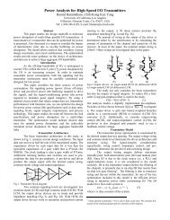
Fig. 3. <strong>BiCMOS</strong> SHA architecture.<br />
(a) (b)<br />
Fig. 4. Modification of conventional bridge to increase the headroom.<br />
This equation suggests a sharp drop in speed if device width<br />
is increased to reduce to a few hundred millivolts<br />
while maintaining the same bias current. For submicron<br />
Fig. 5. Effect of slew rate if sI turns off before sPX<br />
Fig. 6. Hold mode offset generated when sP turns off before sIX<br />
devices, on the other h<strong>and</strong>, simulations imply a trend close to<br />
High-speed bipolar <strong>sample</strong>-<strong>and</strong>-<strong>hold</strong> circuits have traditionally<br />
employed diode bridges for the best trade-off between<br />
speed <strong>and</strong> resolution. Fig. 2(a) illustrates such an implementation.<br />
In addition to the bridge, the circuit incorporates clamp<br />
diodes <strong>and</strong> to limit the swings at nodes <strong>and</strong><br />
To calculate the minimum supply voltage, the circuit can be<br />
simplified as shown in Fig. 2(b), where it is assumed that<br />
0.8 V, 0.5 V, <strong>and</strong> the minimum voltage<br />
across <strong>and</strong> is 0.5 V. Thus, 3.1 V.<br />
The above observations exemplify the difficulties in scaling<br />
the supply voltage of sampling circuits, indicating the need for<br />
low-voltage sampling techniques.
1328 IEEE JOURNAL OF SOLID-STATE CIRCUITS, VOL. 30, NO. 12, DECEMBER 1995<br />
(a) (b) (c)<br />
Fig. 7. Evolution of the sampling switch.<br />
III. <strong>BiCMOS</strong> SAMPLE-AND-HOLD AMPLIFIER<br />
A. Architecture<br />
The SHA architecture is shown in Fig. 3. It consists of<br />
identical <strong>BiCMOS</strong> switches - equal capacitors <strong>and</strong><br />
<strong>amplifier</strong> <strong>and</strong> a switch driver circuit that interfaces<br />
the input clock <strong>with</strong> <strong>and</strong> Switch is always off, <strong>and</strong> its<br />
role will be explained later. Outputs <strong>and</strong> of the <strong>amplifier</strong><br />
differ by 0.8 V but are identical otherwise.<br />
In the sampling mode, <strong>and</strong> are on, the voltage across<br />
tracks <strong>and</strong> is configured as a unity-gain <strong>amplifier</strong>.<br />
In the transition to the <strong>hold</strong> mode, <strong>and</strong> turn off, <strong>and</strong><br />
maintains a unity-gain loop around In this topology, both<br />
the charge injection of <strong>and</strong> <strong>and</strong> the <strong>hold</strong>-mode droop<br />
appear as a common-mode voltage at the inputs of thereby<br />
allowing the use of smaller values for<br />
a single-ended case.<br />
<strong>and</strong> than in<br />
It is important to note that <strong>with</strong> a 3-V supply, – in<br />
Fig. 3 cannot be easily implemented using only MOS devices.<br />
This is because, as mentioned in Section II, the bias voltage at<br />
<strong>and</strong> is typically around half of the supply voltage, leaving<br />
a small gate-source overdrive for MOS switches connected<br />
to these nodes <strong>and</strong> hence slowing down the acquisition. This<br />
problem is especially acute if low-thres<strong>hold</strong> MOSFET’s are<br />
not available.<br />
The sampling switches used in this paper incorporate bipolar<br />
devices in the signal path. A critical issue in such a design is<br />
the <strong>hold</strong>-mode feedthrough because the junction capacitance of<br />
bipolar transistors can be substantial even when these devices<br />
are off. This translates into a direct trade-off between the<br />
size of the sampling capacitor(s) <strong>and</strong> the magnitude of the<br />
feedthrough signal, thereby limiting the speed. This issue is<br />
addressed in Section III.E.<br />
B. <strong>BiCMOS</strong> Sampling Switch<br />
The implementation of – in Fig. 3 has evolved from<br />
the conventional diode bridge of Fig. 2(b). As illustrated in<br />
Fig. 4(b), to increase the dynamic range, the upper diodes<br />
are removed, <strong>and</strong> the emitter-coupled pair is replaced <strong>with</strong> a<br />
single-ended current switch. These modifications increase the<br />
maximum allowable voltage swings by approximately 1.3 V,<br />
Fig. 8. Switch driver.<br />
allowing a dynamic range of 10 b <strong>with</strong> a 3-V supply. However,<br />
unlike the conventional bridge, in this topology, both <strong>and</strong><br />
must turn off at the end of the acquisition mode.<br />
Since <strong>and</strong> in Fig. 4(b) are driven by inherently different<br />
signal paths, it is difficult to guarantee that they switch<br />
simultaneously. We therefore consider two cases. Suppose<br />
turns off before (Fig. 5). Then, for positive slew rates, most<br />
of flows from , <strong>and</strong> the voltage across remains<br />
relatively constant. For negative slew rates, on the other h<strong>and</strong>,<br />
most of serves to discharge , <strong>and</strong> the output tracks the<br />
input. This effect can also be viewed as slew-dependent switch<br />
on-resistance, resulting in harmonic distortion while turns<br />
off.<br />
In the second case, we assume turns off after (Fig. 6).<br />
Then, the two diodes are off, <strong>and</strong> continues to charge<br />
the capacitor, producing a constant offset in the held value.<br />
This offset is cancelled in the architecture of Fig. 3 because it<br />
appears as a common-mode disturbance. We have chosen this<br />
case <strong>and</strong> implemented proper timing in the switch driver to<br />
guarantee that always turns off before<br />
An interesting point of contrast between the conventional<br />
bridge of Fig. 2(a) <strong>and</strong> the sampling switch of Fig. 4(b) relates<br />
to their pedestal error. In the former circuit, the coupling of<br />
the voltage change at nodes <strong>and</strong> to the output through<br />
the junction capacitance of <strong>and</strong> introduces nonlinearity<br />
unless is made to track [1], [2], a remedy that may<br />
increase the <strong>hold</strong>-mode settling time [3]. In the latter circuit,
RAZAVI: A <strong>200</strong>-MHz <strong>15</strong>-<strong>mW</strong> <strong>BiCMOS</strong> SAMPLE-AND-HOLD AMPLIFIER 1329<br />
(a) (b) (c)<br />
Fig. 9. Evolution of output buffer.<br />
on the other h<strong>and</strong>, there is no such effect, <strong>and</strong> the charge<br />
injection due to <strong>and</strong> —which is relatively independent of<br />
the analog input—is cancelled by the architecture of Fig. 3.<br />
The trade-off is that the shunt path provided by <strong>and</strong><br />
in Fig. 2(a) is not present, making the <strong>hold</strong>-mode feedthrough<br />
larger than that of the conventional bridge.<br />
In Fig. 4(b), diode can be replaced <strong>with</strong> an emitter<br />
follower to reduce the transient currents drawn from the input<br />
(Fig. 7(a)). Since the output inductance of the emitter follower<br />
degrades the settling time, a small resistor is placed in series<br />
<strong>with</strong> to dampen the ringing. The switched current source<br />
can be realized as shown in Fig. 7(b). However, the small<br />
transconductance of <strong>and</strong> the large capacitance at node<br />
yield a time constant greater than 1 ns. Note that the<br />
time constant itself increases as turns off, slowing down<br />
the switching considerably. This issue is resolved using two<br />
techniques as illustrated in Fig. 7(c). First, to minimize the<br />
aperture window, emitter follower is added so that it<br />
rapidly pulls node high when <strong>and</strong> must turn off.<br />
Second, to speed up the turn-on, an additional impulse of<br />
current is pulled from on the proper clock edge, thereby<br />
discharging node quickly. The switched current source<br />
is also accompanied <strong>with</strong> such an impulse to match the initial<br />
surge in the drain current of Note that <strong>and</strong><br />
their associated current sources can be shared among several<br />
sampling switches. The clock signals <strong>and</strong> current impulses<br />
required by the <strong>BiCMOS</strong> switch are generated by the switch<br />
driver.<br />
C. Switch Driver<br />
Fig. 8 shows the switch driver <strong>and</strong> its interface <strong>with</strong> the<br />
<strong>BiCMOS</strong> sampling switch The driver consists of: an input<br />
differential pair providing complementary clocks for <strong>and</strong><br />
a slow/fast network <strong>and</strong> <strong>and</strong><br />
<strong>and</strong> operating as switched current sources. Capacitors<br />
<strong>and</strong> couple the logic transitions at the emitter of to the<br />
bases of <strong>and</strong> respectively, thus producing impulses<br />
0.3 ns wide in <strong>and</strong> The final current levels are set<br />
primarily by the collector current of <strong>and</strong> sizing of <strong>and</strong><br />
Fig. 10. Feedthrough cancellation.<br />
In the circuit of Fig. 8, the tail current of – is<br />
approximately equal to 0.25 mA <strong>and</strong> k The<br />
collector current of in the acquisition mode is about 1 mA,<br />
0.5 pF, <strong>and</strong> has a m m to supply<br />
0.5 mA <strong>with</strong> a small gate-source overdrive voltage.<br />
As mentioned previously, the switch driver must turn off<br />
before to avoid harmonic distortion in the <strong>sample</strong>d<br />
signal. To underst<strong>and</strong> how this timing is guaranteed, suppose
1330 IEEE JOURNAL OF SOLID-STATE CIRCUITS, VOL. 30, NO. 12, DECEMBER 1995<br />
Fig. 11. Die photograph.<br />
(a) (b)<br />
Fig. 12. Measured output at <strong>200</strong>-MHz sampling rate <strong>with</strong> analog input at (a) 25 MHz. (b) 50 MHz.<br />
in Fig. 8, turns off, <strong>and</strong> turns on. Then, the voltage at<br />
node (collector of ) begins to fall from directly<br />
reducing the base voltage of through <strong>and</strong> <strong>and</strong><br />
the base voltage of through Therefore, a change of<br />
approximately 10 kT/q in is sufficient to turn off both<br />
<strong>and</strong> However, the long time constant at node (before<br />
turns on) delays the turn-off of We also note that<br />
since (at the collector of ) begins from 1.5 V<br />
<strong>and</strong> reaches V 10 kT/q when has dropped by<br />
10 kT/q, is still off when <strong>and</strong> turn off.<br />
In the switch driver, the current through <strong>and</strong> hence the<br />
collector current of are supply-dependent. This problem<br />
can be solved by means of a replica cancellation circuit.<br />
D. Output Buffer<br />
The <strong>amplifier</strong> in Fig. 3 must efficiently drive the input<br />
capacitance of the following A/D converter. While it is<br />
desirable to employ MOS devices at the input of so as<br />
to achieve a low droop rate, the low open-loop gain <strong>and</strong><br />
high closed-loop output impedance of such an implementation<br />
severely limit the output settling speed (as was noted for<br />
the CMOS op amp of Fig. 1). Fig. 9 illustrates the evolution<br />
of the <strong>amplifier</strong> topology. Shown in Fig. 9(a) is a <strong>BiCMOS</strong><br />
unity-gain stage <strong>with</strong> low output impedance but consuming<br />
a voltage headroom of<br />
2.5 V. To relax the headroom constraint, a level shifter can<br />
be placed in series <strong>with</strong> the base of as depicted in<br />
Fig. 9(b).<br />
In Fig. 9(b), the circuit comprising <strong>and</strong><br />
happens to be the same as the sampling switch of Fig. 7(c)<br />
<strong>and</strong> can operate as such, thereby performing the role of in<br />
Fig. 3. In order to maintain feedback after this switch turns off,<br />
another emitter follower <strong>and</strong> a capacitor are added<br />
as shown in Fig. 9(c).
RAZAVI: A <strong>200</strong>-MHz <strong>15</strong>-<strong>mW</strong> <strong>BiCMOS</strong> SAMPLE-AND-HOLD AMPLIFIER 1331<br />
Fig. 13. Hold mode droop <strong>and</strong> pedestal.<br />
Fig. 14. Hold mode feedthrough <strong>with</strong> 50-MHz analog input.<br />
Note that the small-signal resistance of slightly degrades<br />
the <strong>amplifier</strong> phase margin but is sized such that its<br />
base-collector capacitance 100 fF) compensates the circuit<br />
reliably.<br />
In this circuit, the input differential pair has a tail current<br />
of 0.2 mA, <strong>and</strong> the output transistor is biased at 2 mA.<br />
E. Feedthrough Cancellaation<br />
As mentioned in Section III.A, the diode switches introduce<br />
significant feedthrough of the analog input during the <strong>hold</strong><br />
mode, necessitating the use of large sampling capacitor(s).<br />
In the architecture of Fig. 3, this limitation is overcome by<br />
allowing <strong>and</strong> conduct equal feedthrough signals to<br />
both inputs of the <strong>amplifier</strong> (Fig. 10). This technique remains<br />
effective as long as the output impedance seen at node<br />
is sufficiently small. It can be shown that if the open-loop<br />
gain <strong>and</strong> output impedance of the <strong>amplifier</strong> are <strong>and</strong><br />
Fig. <strong>15</strong>. Output spectrum <strong>with</strong> <strong>200</strong>-MHz sampling rate <strong>and</strong> 10-MHz input<br />
(Horiz., 5 MHz/div.; Vert., 10 dB/div.).<br />
Fig. 16. Output harmonic distortion as a function of analog input frequency<br />
<strong>with</strong> a sampling rate of <strong>200</strong> MHz.<br />
respectively, then the net feedthrough is given by<br />
where is the total feedthrough capacitance of each switch<br />
(assumed to be much less than <strong>and</strong> ).<br />
Simulations indicate that the net feedthrough is 60 dB below<br />
the analog input for frequencies as high as 100 MHz.<br />
IV. EXPERIMENTAL RESULTS<br />
The <strong>sample</strong>-<strong>and</strong>-<strong>hold</strong> <strong>amplifier</strong> has been fabricated in a 20-<br />
GHz 1- m <strong>BiCMOS</strong> technology [4]. Shown in Fig. 11 is<br />
a photograph of the prototype, whose active area measures<br />
approximately 220 m <strong>15</strong>0 m. The circuit has been tested<br />
on wafer using Cascade probes <strong>and</strong> a Tektronix active probe.<br />
All tests have been performed <strong>with</strong> a 3-V supply. The SHA<br />
dissipates <strong>15</strong> <strong>mW</strong>: 7 <strong>mW</strong> in 6<strong>mW</strong>in <strong>and</strong> <strong>and</strong> 2<br />
<strong>mW</strong> in the switch driver.<br />
Since the SHA is not capable of driving a 50- load,<br />
accurate measurement of its acquisition <strong>and</strong> <strong>hold</strong> settling times<br />
(4)
1332 IEEE JOURNAL OF SOLID-STATE CIRCUITS, VOL. 30, NO. 12, DECEMBER 1995<br />
TABLE I<br />
SHA CHARACTERISTICS<br />
has not been possible. Simulations suggest a 10-b acquisition<br />
time of 2.2 ns <strong>and</strong> a <strong>hold</strong> settling time of 1.2 ns.<br />
Table I summarizes the performance of the <strong>BiCMOS</strong> SHA.<br />
Fig. 12(a) <strong>and</strong> (b) show the measured output at <strong>200</strong>-MHz<br />
sampling rate <strong>with</strong> input sinewaves of 25 <strong>and</strong> 50 MHz,<br />
respectively. Fig. 13 depicts the droop in the <strong>hold</strong> mode,<br />
indicating a droop rate of approximately 40 V/ns. The<br />
pedestal error is approximately equal to 8 mV. The <strong>hold</strong>-mode<br />
feedthrough <strong>with</strong> a 50-MHz analog input is roughly 52 dB,<br />
as shown in Fig. 14. The accuracy of this measurement is<br />
limited by ground feedthrough in the setup.<br />
The <strong>sample</strong>d waveform has also been examined for harmonic<br />
distortion. In this test, the SHA output is applied to a<br />
resistive divider feeding a spectrum analyzer. Fig. <strong>15</strong> shows<br />
the resulting spectrum <strong>with</strong> <strong>200</strong>-MHz sampling rate <strong>and</strong> 10-<br />
MHz analog input, exhibiting a distortion less than 65 dB.<br />
Plotted in Fig. 16 is the distortion as a function of the analog<br />
input frequency while the SHA <strong>sample</strong>s at <strong>200</strong> MHz. Note<br />
that this measurement includes the output slewing during the<br />
acquisition mode, a substantial source of nonlinearity. It is<br />
expected that if only the held values are considered, much<br />
lower distortion will be observed.<br />
V. CONCLUSION<br />
High-speed <strong>sample</strong>-<strong>and</strong>-<strong>hold</strong> <strong>amplifier</strong>s can employ lowvoltage<br />
techniques to provide 10 b of dynamic range in a<br />
3-V system <strong>with</strong> low power dissipation. The availability of<br />
both bipolar <strong>and</strong> MOS devices on the same substrate makes<br />
it possible to design low-voltage high-performance sampling<br />
switches <strong>and</strong> <strong>amplifier</strong>s. A <strong>sample</strong>-<strong>and</strong>-<strong>hold</strong> circuit using such<br />
topologies has been designed <strong>and</strong> fabricated in a 1- m 20-<br />
GHz <strong>BiCMOS</strong> technology. Operating at <strong>200</strong> MHz, the SHA<br />
dissipates <strong>15</strong> <strong>mW</strong> from a 3-V supply <strong>and</strong> accommodates<br />
input/output swings of 1.5 V.<br />
REFERENCES<br />
[1] B. Razavi, Principles of Data Conversion System Design. New York:<br />
IEEE Press, 1995.<br />
[2] K. Poulton, J. S. Kang, <strong>and</strong> J. J. Corcoran, “A 2 Gs/s HBT <strong>sample</strong> <strong>and</strong><br />
<strong>hold</strong>,” in Tech. Dig. IEEE GaAs IC Symp., 1988, pp. 199–202.<br />
[3] W. T. Colleran <strong>and</strong> A. A. Abidi, “A 10-b 75-MHz two-step pipelined<br />
bipolar A/D converter,” IEEE J. Solid-State Circuits, vol. 28, pp.<br />
1187–1199, Dec. 1993.<br />
[4] J. Sung et al., “BEST2—A high performance super self-aligned 3 V/5<br />
V <strong>BiCMOS</strong> technology <strong>with</strong> extremely low parasitics for low-power<br />
mixed-signal applications,” in Proc. CICC, May 1994, pp. <strong>15</strong>–18.<br />
Behzad Razavi, (S’87–M’90) for a photograph <strong>and</strong> biography, see p. 109 of<br />
the February 1995 issue of this JOURNAL.