

HALF-BRIDGE GATE DRIVER IC - International Rectifier
HALF-BRIDGE GATE DRIVER IC - International Rectifier
HALF-BRIDGE GATE DRIVER IC - International Rectifier
- TAGS
- rectifier
- www.irf.com

Create successful ePaper yourself
Turn your PDF publications into a flip-book with our unique Google optimized e-Paper software.
Features<br />
• Floating channel up to 600 V or 1200 V<br />
• Soft over-current shutdown<br />
• Synchronization signal to synchronize shutdown with the other phases<br />
• Integrated desaturation detection circuit<br />
• Two stage turn on output for di/dt control<br />
• Separate pull-up/pull-down output drive pins<br />
• Matched delay outputs<br />
• Undervoltage lockout with hysteresis band<br />
• Lead free<br />
Description<br />
The IR2114/IR2214 gate driver family is suited to drive a single half bridge in<br />
power switching applications. These drivers provide high gate driving<br />
capability (2 A source, 3 A sink) and require low quiescent current, which<br />
allows the use of bootstrap power supply techniques in medium power<br />
systems. These drivers feature full short circuit protection by means of power<br />
transistor desaturation detection and manage all half-bridge faults by<br />
smoothly turning off the desaturated transistor through the dedicated soft<br />
shutdown pin, therefore preventing over-voltages and reducing<br />
electromagnetic emissions. In multi-phase systems, the IR2114/IR2214<br />
drivers communicate using a dedicated local network (SY_FLT and<br />
FAULT/SD signals) to properly manage phase-to-phase short circuits. The<br />
system controller may force shutdown or read device fault state through the<br />
3.3 V compatible CMOS I/O pin (FAULT/SD). To improve the signal immunity<br />
from DC-bus noise, the control and power ground use dedicated pins<br />
enabling low-side emitter current sensing as well. Undervoltage conditions in<br />
floating and low voltage circuits are managed independently.<br />
Typical connection<br />
Data Sheet No. PD60213 revL<br />
IR2114SSPbF/IR2214SSPbF<br />
<strong>HALF</strong>-<strong>BRIDGE</strong> <strong>GATE</strong> <strong>DRIVER</strong> <strong>IC</strong><br />
Product Summary<br />
VOFFSET<br />
600 V or<br />
1200 V max.<br />
IO+/- (min) 1.0 A / 1.5 A<br />
www.irf.com 14-Aug-09 © 2009 <strong>International</strong> <strong>Rectifier</strong><br />
1<br />
VOUT<br />
10.4 V – 20 V<br />
Deadtime matching (max) 75 ns<br />
Deadtime (typ) 330 ns<br />
Desat blanking time (typ) 3 µs<br />
DSH, DSL input voltage<br />
threshold (typ)<br />
8.0 V<br />
Soft shutdown time (typ) 9.25 µs<br />
Package<br />
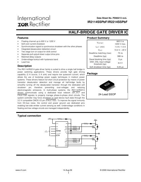
24-Lead SSOP
IR2114/IR2214SSPbF<br />
Absolute Maximum Ratings<br />
Absolute maximum ratings indicate sustained limits beyond which damage to the device may occur. All voltage<br />
parameters are absolute voltages referenced to VSS, all currents are defined positive into any lead The thermal resistance<br />
and power dissipation ratings are measured under board mounted and still air conditions.<br />
Symbol Definition Min. Max. Units<br />
VS High side offset voltage VB - 25 VB + 0.3<br />
VB High side floating supply voltage<br />
IR2114<br />
IR2214<br />
-0.3<br />
-0.3<br />
625<br />
1225<br />
VHO High side floating output voltage (HOP, HON and SSDH) VS - 0.3 VB + 0.3<br />
VCC Low side and logic fixed supply voltage -0.3 25<br />
COM Power ground VCC - 25 VCC + 0.3<br />
VLO Low side output voltage (LOP, LON and SSDL) VCOM -0.3 VCC + 0.3<br />
VIN Logic input voltage (HIN, LIN and FLT_CLR) -0.3 VCC + 0.3<br />
VFLT Fault input/output voltage (FAULT/SD and SY_FLT) -0.3 VCC + 0.3<br />
VDSH High side DS input voltage VS -3 VB + 0.3<br />
VDSL Low side DS input voltage VCOM -3 VCC + 0.3<br />
dVs/dt Allowable offset voltage slew rate — 50 V/ns<br />
PD Package power dissipation @ TA ≤ 25 °C — 1.5 W<br />
RthJA Thermal resistance, junction to ambient — 65 °C/W<br />
TJ Junction temperature — 150<br />
TS Storage temperature -55 150<br />
TL Lead temperature (soldering, 10 seconds) — 300<br />
Recommended Operating Conditions<br />
For proper operation the device should be used within the recommended conditions. All voltage parameters are absolute<br />
voltages referenced to VSS. The VS offset rating is tested with all supplies biased at a 15 V differential.<br />
Symbol Definition Min. Max. Units<br />
VB High side floating supply voltage † VS + 11.5 VS + 20<br />
VS High side floating supply offset voltage<br />
IR2114 VSS 600<br />
††<br />
IR2214 VSS 1200<br />
VHO High side output voltage (HOP, HON and SSDH) VS VS + 20<br />
VLO Low side output voltage (LOP, LON and SSDL) VCOM VCC<br />
VCC Low side and logic fixed supply voltage (Note 1) 11.5 20<br />
COM Power ground -5 5<br />
VIN Logic input voltage (HIN, LIN and FLT_CLR) VSS VCC<br />
VFLT Fault input/output voltage (FAULT/SD and SY_FLT) VSS VCC<br />
VDSH High side DS pin input voltage VS - 2.0 VB<br />
VDSL Low side DS pin input voltage VCOM - 2.0 VCC<br />
tPWHIN High side pulse width for HIN input 1 µs<br />
TA Ambient temperature -40 125 °C<br />
† While internal circuitry is operational below the indicated supply voltages, the UV lockout disables the output<br />
drivers if the UV thresholds are not reached. A minimum supply voltage of 8V is recommended for the driver<br />
to operate safely under switching conditions at VS pin (please refer to the “start-up sequence” in application<br />
section of this document)<br />
†† Logic operational for VS from VSS-5 V to VSS +600 V or 1200 V. Logic state held for VS from VSS -5 V to VSS-<br />
VBS. For a negative spike on VB (referenced to VSS) of less than 200ns the <strong>IC</strong> will withstand a sustained peak<br />
of -40V under normal operation and an isolated event of up to -70V peak spike (please refer to the Design<br />
Tip DT97-3 for more details).<br />
www.irf.com © 2009 <strong>International</strong> <strong>Rectifier</strong><br />
2<br />
V<br />
°C<br />
V
Static Electrical Characteristics<br />
VCC = 15 V, VSS = COM = 0 V, VS = 600 V or 1200 V and TA = 25 °C unless otherwise specified.<br />
Pins: VCC, VSS, VB, VS (refer to Fig. 1)<br />
IR2114/IR2214SSPbF<br />
Symbol Definition Min Typ Max Units Test Conditions<br />
VCCUV+ VCC supply undervoltage positive going threshold 9.3 10.2 11.4<br />
VCCUV- VCC supply undervoltage negative going threshold 8.7 9.3 10.3<br />
VCCUVH VCC supply undervoltage lockout hysteresis — 0.9 —<br />
VBSUV+ (VB-VS) supply undervoltage positive going threshold 9.3 10.2 11.4<br />
VBSUV- (VB-VS) supply undervoltage negative going threshold 8.7 9.3 10.3<br />
VBSUVH (VB-VS) supply undervoltage lockout hysteresis — 0.9 —<br />
ILK Offset supply leakage current — — 50<br />
IQBS Quiescent VBS supply current — 400 800<br />
VS = 0 V, VS = 600 V<br />
or 1200 V<br />
www.irf.com © 2009 <strong>International</strong> <strong>Rectifier</strong><br />
3<br />
V<br />
µA<br />
VB = VS = 600 V or<br />
1200 V<br />
VIN = 0 V or 3.3 V<br />
IQCC Quiescent VCC supply current — 0.7 2.5 mA no load<br />
Pins: HIN, LIN, FLTCLR, FAULT/SD, SY_FLT (refer to Fig. 2, 3)<br />
Symbol Definition Min Typ Max Units Test Conditions<br />
VIH Logic "1" input voltage 2.0 — —<br />
VIL Logic "0" input voltage — — 0.8<br />
VIHSS Logic input hysteresis 0.2 0.4 —<br />
IIN+<br />
IIN-<br />
Logic “1” input bias current (HIN, LIN, FLTCLR) — 330 —<br />
Logic “0” input bias current (FAULT/SD, SY_FLT) 0 — 1<br />
Logic “0” input bias current -1 — 0<br />
Logic “1” input bias current (FAULT/SD, SY_FLT) -1 — 0<br />
RON,FLT FAULT/SD open drain resistance — 60 —<br />
RON,SY SY_FLT open drain resistance — 60 —<br />
Pins: DSL, DSH (refer to Fig. 4)<br />
VDESAT, IDS and IDSB parameters are referenced to COM and VS respectively for DSL and DSH.<br />
Symbol Definition Min Typ Max Units Test Conditions<br />
VDESAT+ High desat input threshold voltage 7.2 8.0 8.8<br />
VDESAT- Low desat input threshold voltage 6.3 7.0 7.7<br />
VDSTH Desat input voltage hysteresis — 1.0 —<br />
V<br />
µA<br />
V See Figs. 4,16<br />
IDS+ High DSH or DSL input bias current — 21 — VDESAT = VCC or VBS<br />
IDS- Low DSH or DSL input bias current — -160 — µA<br />
VDESAT = 0 V<br />
Ω<br />
VCC = VCCUV-<br />
to 20 V<br />
VIN = 3.3 V<br />
VIN = 0 V<br />
PW≤ 7 µs
Pins: HOP, LOP (refer to Fig. 5)<br />
IR2114/IR2214SSPbF<br />
Symbol Definition Min Typ Max Units Test Conditions<br />
VOH High level output voltage, VB – VHOP or VCC –VLOP — 40 300 mV IO= 20 mA<br />
IO1+ Output high first stage short circuit pulsed current 1 2 —<br />
IO2+<br />
Output high second stage short circuit pulsed current<br />
Pins: HON, LON, SSDH, SSDL (refer to Fig. 6)<br />
0.5 1 —<br />
VHOP/LOP= 0 V, HIN<br />
or LIN = 1, PW≤<br />
200 ns, resistive<br />
load, see Fig. 8<br />
www.irf.com © 2009 <strong>International</strong> <strong>Rectifier</strong><br />
4<br />
A<br />
VHOP/LOP= 0 V, HIN<br />
or LIN= 1,<br />
400 ns ≤PW≤ 10<br />
µs, resistive load,<br />
see Fig. 8<br />
Symbol Definition Min Typ Max Units Test Conditions<br />
VOL Low level output voltage, VHON or VLON — 45 300 mV IO= 20 mA<br />
RON,SSD Soft Shutdown on resistance † — 90 — Ω PW≤ 7 µs<br />
IO- Output low short circuit pulsed current 1.5 3 — A<br />
† SSD operation only<br />
VHOP/LOP = 15 V,<br />
HIN or LIN = 0, PW≤<br />
10 µs
AC Electrical Characteristics<br />
VCC = VBS = 15 V, VS = VSS and TA = 25 °C unless otherwise specified.<br />
IR2114/IR2214SSPbF<br />
Symbol Definition Min. Typ. Max. Units Test Conditions<br />
ton Turn on propagation delay 220 440 660<br />
toff Turn off propagation delay 220 440 660<br />
tr Turn on rise time (CLOAD=1 nF) — 24 —<br />
tf Turn off fall time (CLOAD=1 nF) — 7 —<br />
VIN = 0 & 1, VS = 0 V to 600 V<br />
or 1200 V,<br />
HOP shorted to HON, LOP<br />
shorted to LON, Fig. 7<br />
ton1 Turn on first stage duration time 120 200 280 Fig. 8<br />
tDESAT1<br />
tDESAT2<br />
tDESAT3<br />
tDESAT4<br />
DSH to HO soft shutdown propagation delay at HO<br />
turn on<br />
DSH to HO soft shutdown propagation delay after<br />
blanking<br />
DSL to LO soft shutdown propagation delay at LO<br />
turn on<br />
DSL to LO soft shutdown propagation delay after<br />
blanking<br />
2000 3300 4600 VHIN= 1 V<br />
1050 — — VDESAT = 15 V, Fig. 10<br />
2000 3300 4600 VLIN = 1 V<br />
1050 — — VDESAT = 15 V, Fig. 10<br />
tDS Soft shutdown minimum pulse width of desat 1000 — — Fig. 9<br />
tSS Soft shutdown duration period 5700 9250 13500 VDS=15 V, Fig. 9<br />
tSY_FLT,<br />
DESAT1<br />
tSY_FLT,<br />
DESAT2<br />
tSY_FLT,<br />
DESAT3<br />
tSY_FLT,<br />
DESAT4<br />
DSH to SY_FLT propagation delay at HO turn on<br />
ns<br />
— 3600 — VHIN = 1 V<br />
DSH to SY_FLT propagation delay after blanking 1300 — — VDS = 15 V, Fig. 10<br />
DSL to SY_FLT propagation delay at LO turn on — 3050 — VLIN = 1 V<br />
DSL to SY_FLT propagation delay after blanking 1050 — — VDESAT=15 V, Fig. 10<br />
tBL DS blanking time at turn on — 3000 —<br />
Deadtime/Delay Matching Characteristics<br />
VHIN = VLIN = 1 V, VDESAT=15 V,<br />
Fig. 10<br />
DT Deadtime — 330 — Fig. 11<br />
MDT Deadtime matching, MDT=DTH-DTL — — 75 External DT = 0 s, Fig. 11<br />
PDM<br />
Propagation delay matching,<br />
Max (ton, toff) – Min (ton, toff)<br />
— — 75<br />
External DT > 500 ns, Fig. 7<br />
www.irf.com © 2009 <strong>International</strong> <strong>Rectifier</strong><br />
5
VCC/VB<br />
VSS/VS<br />
FAULT/SD<br />
SY_FLT<br />
on/off<br />
internal signal<br />
VSS<br />
comparator<br />
VCCUV/VBSUV<br />
UV internal<br />
signal<br />
HIN/LIN/<br />
FLTCLR<br />
IR2114/IR2214SSPbF<br />
Figure 1: Undervoltage Diagram Figure 2: HIN, LIN and FLTCLR Diagram<br />
R ON<br />
Figure 3: FAULT/SD and SY_FLT Diagram Figure 4: DSH and DSL Diagram<br />
200ns<br />
oneshot<br />
schmitt<br />
trigger<br />
fault/hold<br />
internal signal<br />
VCC/VB<br />
VOH<br />
LOP/HOP<br />
Figure 5: HOP and LOP Diagram Figure 6: HON, LON, SSDH and SSDL Diagram<br />
www.irf.com © 2009 <strong>International</strong> <strong>Rectifier</strong><br />
6<br />
VSS<br />
VCC/VBS<br />
DSL/DSH<br />
V DESAT<br />
COM/VS<br />
on/off<br />
internal signal<br />
desat<br />
internal signal<br />
10k<br />
100k<br />
700k<br />
schmitt<br />
trigger<br />
comparator<br />
RON,SSD<br />
internal<br />
signal<br />
LON/HON<br />
SSDL/SSDH<br />
VOL<br />
COM/VS<br />
SSD internal<br />
signal
HIN<br />
LIN<br />
HO (HOP=HON)<br />
LO (LOP=LON)<br />
HIN/LIN<br />
DSH/DSL<br />
t on<br />
SSD Driver Enable<br />
HO/LO<br />
50% 50%<br />
t r<br />
10%<br />
PWin<br />
PWout<br />
90% 90%<br />
Figure 7: Switching Time Waveforms<br />
Io1+<br />
IR2114/IR2214SSPbF<br />
www.irf.com © 2009 <strong>International</strong> <strong>Rectifier</strong><br />
7<br />
Ton1<br />
Io2+<br />
Figure 8: Output Source Current<br />
t DS<br />
8V 8V<br />
t DESAT<br />
t SS<br />
Figure 9: Soft Shutdown Timing Waveform<br />
3.3V<br />
t off<br />
3.3V<br />
t f<br />
10%
50%<br />
HIN<br />
LIN<br />
DSH<br />
DSL<br />
SY_FLT<br />
FAULT/SD<br />
FLTCLR<br />
8V<br />
tSY_FLT,DESAT1<br />
tDESAT1<br />
50%<br />
10%<br />
HON<br />
tBL<br />
LON<br />
LIN<br />
HIN<br />
50%<br />
90%<br />
SoftShutdown<br />
Turn-On Propagation Delay<br />
HO (HOP=HON)<br />
LO (LOP=LON)<br />
tSY_FLT,DESAT2<br />
50%<br />
tDESAT2<br />
tBL<br />
8V<br />
50%<br />
90% SoftShutdown<br />
50%<br />
8V 8V<br />
50%<br />
10%<br />
tSY_FLT,DESAT3<br />
tDESAT3<br />
tBL<br />
90%<br />
SoftShutdown<br />
IR2114/IR2214SSPbF<br />
90% SoftShutdown<br />
www.irf.com © 2009 <strong>International</strong> <strong>Rectifier</strong><br />
8<br />
50%<br />
Turn-On Propagation Delay<br />
Figure 10: Desat Timing<br />
50% 50%<br />
50%<br />
50%<br />
tSY_FLT,DESAT4<br />
tDESAT4<br />
50% 50%<br />
DTH DTL<br />
MDT=DTH-DTL<br />
Figure 11: Internal Deadtime Timing<br />
tBL<br />
50%<br />
90%<br />
Turn_Off propagation Delay<br />
50%<br />
90%<br />
50%
Lead Assignments<br />
24-Lead SSOP<br />
Lead Definitions<br />
Symbol Description<br />
VCC<br />
VSS<br />
Low side gate driver supply<br />
Logic ground<br />
HIN Logic input for high side gate driver outputs (HOP/HON)<br />
IR2114/IR2214SSPbF<br />
LIN Logic input for low side gate driver outputs (LOP/LON)<br />
Dual function (in/out) active low pin. Refer to Figs. 15, 17, and 18. As an output, indicates fault condition.<br />
FAULT/SD As an input, shuts down the outputs of the gate driver regardless HIN/LIN status.<br />
Dual function (in/out) active low pin. Refer to Figs. 15, 17, and 18. As an output, indicates SSD sequence<br />
SY_FLT is occurring. As an input, an active low signal freezes both output status.<br />
FLT_CLR Fault clear active high input. Clears latched fault condition (see Fig. 17)<br />
LOP Low side driver sourcing output<br />
LON Low side driver sinking output<br />
DSL Low side IGBT desaturation protection input<br />
SSDL Low side soft shutdown<br />
COM Low side driver return<br />
VB<br />
High side gate driver floating supply<br />
HOP High side driver sourcing output<br />
HON High side driver sinking output<br />
DSH High side IGBT desaturation protection input<br />
SSDH High side soft shutdown<br />
VS<br />
High side floating supply return<br />
HIN<br />
LIN<br />
FLT_CLR<br />
SY_FLT<br />
FAULT/SD<br />
VSS<br />
SSDL<br />
COM<br />
LON<br />
LOP<br />
VCC<br />
DSL<br />
SSOP24<br />
www.irf.com © 2009 <strong>International</strong> <strong>Rectifier</strong><br />
9<br />
1<br />
12<br />
24<br />
13<br />
DSH<br />
VB<br />
N.C.<br />
HOP<br />
HON<br />
VS<br />
SSDH<br />
N.C.<br />
N.C.<br />
N.C.<br />
N.C.<br />
N.C.
VCC<br />
HIN<br />
LIN<br />
SY_FLT<br />
FAULT/SD<br />
FLT_CLR<br />
VSS<br />
UV_VCC<br />
DETECT<br />
SSD<br />
FAULT<br />
SCHMITT<br />
TRIGGER<br />
INPUT<br />
SHOOT<br />
THROUGH<br />
PREVENTION<br />
(DT) Deadtime<br />
FAULT<br />
UV_VCC<br />
FLT_CLR<br />
Soft<br />
ShutDown<br />
HOLD<br />
SD<br />
DESAT<br />
EVENT<br />
Stable State<br />
− FAULT<br />
− HO=LO=0 (Normal operation)<br />
− HO/LO=1 (Normal operation)<br />
− UNDERVOLTAGE VCC<br />
− SHUTDOWN (SD)<br />
− UNDERVOLTAGE VBS<br />
− FREEZE<br />
INPUT<br />
HOLD<br />
LOG<strong>IC</strong><br />
internal Hold<br />
OUTPUT<br />
SHUTDOWN<br />
LOG<strong>IC</strong><br />
Hard ShutDown<br />
FAULT LOG<strong>IC</strong><br />
managemend<br />
(See figure 14)<br />
on/off (HS)<br />
on/off (LS)<br />
DesatHS<br />
DesatLS<br />
LEVEL<br />
SHIFTERS<br />
IR2114/IR2214SSPbF<br />
www.irf.com © 2009 <strong>International</strong> <strong>Rectifier</strong><br />
10<br />
on/off<br />
desat<br />
LATCH<br />
LOCAL DESAT<br />
PROTECTION<br />
SOFT SHUTDOWN<br />
UV_VBS DETECT<br />
LOCAL DESAT<br />
PROTECTION<br />
SOFTSHUTDOWN<br />
FUNCTIONAL BLOCK DIAGRAM<br />
DSH/L<br />
HIN/LIN<br />
Start-Up<br />
Sequence<br />
HO/LO=1<br />
SY_FLT<br />
HO=LO=0<br />
HIN/LIN<br />
SY_FLT<br />
UnderVoltage<br />
VCC<br />
HO=LO=0<br />
UV_VCC<br />
UV_VBS<br />
FAULT/SD<br />
UV_VCC<br />
FAULT/SD<br />
UV_VBS<br />
FAULT/SD<br />
FAULT/SD<br />
UnderVoltage<br />
VBS<br />
HO=0, LO=LIN<br />
UV_VCC<br />
STATE DIAGRAM<br />
Temporary State<br />
− SOFT SHUTDOWN<br />
− START UP SEQUENCE<br />
SY_FLT<br />
Freeze<br />
DSH/L<br />
ShutDown<br />
FAULT/SD<br />
on/off<br />
soft<br />
shutdown<br />
on/off<br />
soft<br />
shutdown<br />
System Variable<br />
− FLT_CLR<br />
− HIN/LIN<br />
− UV_VCC<br />
− UV_VBS<br />
− DSH/L<br />
− SY_FLT<br />
− FAULT/SD<br />
di/dt control<br />
Driver<br />
di/dt control<br />
Driver<br />
NOTE 1: A change of logic value of the signal labeled on lines (system variable) generates a state transition.<br />
NOTE 2: Exiting from UNDERVOLTAGE VBS state, the HO goes high only if a rising edge event happens in HIN.<br />
VB<br />
HOP<br />
HON<br />
SSDH<br />
DSH<br />
VS<br />
LOP<br />
LON<br />
SSDL<br />
DSL<br />
COM
Operation<br />
Hin<br />
HO/LO Status HOP/LOP HON/LON SSDH/SSDL<br />
0 HiZ 0 HiZ<br />
1 1 HiZ HiZ<br />
SSD HiZ HiZ 0<br />
LO/HO Output follows inputs (in=1->out=1, in=0->out=0)<br />
Output keeps previous status<br />
LOn-1/HOn-1<br />
INPUTS<br />
Lin<br />
Logic Table: Output Drivers Status Description<br />
FLT_CLR<br />
______<br />
SY_FLT<br />
SSD: desat (out)<br />
HOLD: freezing<br />
(in)<br />
INPUT/OUTPUT<br />
_________<br />
FAULT/SD<br />
SD: shutdown (in)<br />
FAULT: diagnostic<br />
(out)<br />
IR2114/IR2214SSPbF<br />
Undervoltage<br />
Yes: V< UV<br />
threshold<br />
No : V> UV<br />
threshold<br />
X: don’t care<br />
OUTPUTS<br />
VCC VBS HO LO<br />
Shutdown X X X X 0 (SD) X X 0 0<br />
Fault Clear HIN LIN X † (FAULT) No No HO LO<br />
Fault Cleared HIN LIN 1 X 1 †† No No HO LO<br />
Normal<br />
Operation<br />
1 0 0 1 1 No No 1 0<br />
0 1 0 1 1 No No 0 1<br />
0 0 0 1 1 No No 0 0<br />
Anti Shoot<br />
Through<br />
1 1 0 1 1 No No 0 0<br />
Soft<br />
Shutdown<br />
(entering)<br />
1<br />
0<br />
0<br />
1<br />
0<br />
0<br />
(SSD)<br />
(SSD)<br />
1<br />
1<br />
No<br />
No<br />
No<br />
No<br />
SSD<br />
0<br />
0<br />
SSD<br />
Soft X X 0 (SSD) (FAULT) No No 0 0<br />
Shutdown<br />
(finishing) X X 0 (SSD) (FAULT) No No 0 0<br />
Freeze X X X 0 (HOLD) 1 No No HOn-1 LOn-1<br />
Undervoltage<br />
X LIN X 1 1 No Yes 0 LO<br />
X X X 1 0 (FAULT) Yes X 0 0<br />
† SY_FLT automatically resets after the SSD event is over, without requiring FLT_CLR to be asserted. To<br />
avoid FLT_CLR conflicting with the SSD sequence of operations, in the event of a SSD during normal<br />
operation it is recommended not to apply FLT_CLR while SY_FLT is active. At power supply start-up<br />
instead, it is recommended to keep FLT_CLR active to prevent spurious diagnostic signals being<br />
generated, as described in section 1.1 Start-Up Sequence and in section 1.4.5 Fault Management at<br />
Start-up.<br />
†† Holding FLT_CLR high all time will not allow the gate driver to latch the FAULT status and migth<br />
compromise power system protection.<br />
www.irf.com © 2009 <strong>International</strong> <strong>Rectifier</strong><br />
11
1 Features Description<br />
1.1 Start-Up Sequence<br />
At power supply start-up, it is recommended to keep the<br />
FLT_CLR pin active until the supply voltages are<br />
properly established. This prevents spurious diagnostic<br />
signals being generated.<br />
When the bootstrap supply topology is used for<br />
supplying the floating high side stage, the following startup<br />
sequence is recommended (see also Fig. 12):<br />
1. Set VCC,<br />
2. Set FLT_CLR pin to HIGH level,<br />
3. Set LIN pin to HIGH level and charge the<br />
bootstrap capacitor,<br />
4. Release LIN pin to LOW level,<br />
5. Release FLT_CLR pin to LOW level.<br />
VCC<br />
FLT_CLR<br />
LIN<br />
LO<br />
Figure 12 Start-Up Sequence<br />
A minimum 15 µs LIN and FLT-CLR pulse is required.<br />
A minimum supply voltage of 8V is recommended for the<br />
driver to operate safely under switching conditions at VS<br />
pin. At lower supply the gate driving capability decreases<br />
and might become not sufficient to counteract switching<br />
charge injected to the outputs.<br />
1.2 Normal Operation Mode<br />
After the start-up sequence has completed, the device<br />
becomes fully operative (see grey blocks in the State<br />
Diagram).<br />
HIN and LIN produce driver outputs to switch<br />
accordingly, while the input logic monitors the input<br />
signals and deadtime (DT) prevent shoot-through events<br />
from occurring.<br />
1.3 Shutdown<br />
The system controller can asynchronously command the<br />
Hard Shutdown (HSD) through the 3.3 V compatible<br />
CMOS I/O FAULT/SD pin. This event is not latched.<br />
In a multi-phase system, FAULT/SD signals are or-ed so<br />
the controller or one of the gate drivers can force the<br />
simultaneous shutdown of the other gate drivers through<br />
the same pin.<br />
1.4 Fault Management<br />
IR2114/IR2214SSPbF<br />
The IR2114/IR2214 is able to manage supply failure<br />
(undervoltage lockout) and transistor desaturation (on<br />
both the low and high side switches).<br />
1.4.1 Undervoltage (UV)<br />
The undervoltage protection function disables the<br />
driver’s output stage which prevents the power device<br />
from being driven when the input voltage is less than the<br />
undervoltage threshold. Both the low side (VCC supplied)<br />
and the floating side (VBS supplied) are controlled by a<br />
dedicate undervoltage function.<br />
An undervoltage event on the VCC pin (when<br />
VCC < UVVCC-) generates a diagnostic signal by forcing<br />
the FAULT/SD pin low (see FAULT/SD section and Fig.<br />
14). This event disables both the low side and floating<br />
drivers and the diagnostic signal holds until the<br />
undervoltage condition is over. The fault condition is not<br />
latched and the FAULT/SD pin is released once VCC<br />
becomes higher than UVVCC+.<br />
The VBS undervoltage protection works by disabling only<br />
the floating driver. Undervoltage on VBS does not prevent<br />
the low side driver from activating its output nor does it<br />
generate diagnostic signals. The VBS undervoltage<br />
condition (VBS < UVVBS-) latches the high side output<br />
stage in the low state. VBS must exceed the UVVBS+<br />
threshold to return the device to its normal operating<br />
mode. To turn on the floating driver, HIN must be reasserted<br />
high (rising edge event on HIN is required).<br />
1.4.2 Power Devices Desaturation<br />
Different causes can generate a power inverter failure<br />
(phase and/or rail supply short-circuit, overload<br />
conditions induced by the load, etc.). In all of these fault<br />
conditions, a large increase in current results in the<br />
IGBT.<br />
The IR2114/IR2214 fault detection circuit monitors the<br />
IGBT emitter to collector voltage (VCE) (an external high<br />
voltage diode is connected between the IGBT’s collector<br />
and the <strong>IC</strong>s DSH or DSL pins). A high current in the<br />
IGBT may cause the transistor to desaturate; this<br />
condition results in an increase of VCE.<br />
Once in desaturation, the current in the power transistor<br />
can be as high as 10 times the nominal current.<br />
Whenever the transistor is switched off, this high current<br />
generates relevant voltage transients in the power stage<br />
that need to be smoothed out in order to avoid<br />
destruction (by over-voltage). The gate driver is able to<br />
control the transient condition by smoothly turning off the<br />
desaturated transistor with its integrated soft shutdown<br />
(SSD) protection.<br />
1.4.3 Desaturation Detection: DSH/L Function<br />
Figure 13 shows the structure of the desaturation<br />
sensing and soft shutdown block. This configuration is<br />
the same for both the high and low side output stages.<br />
www.irf.com © 2009 <strong>International</strong> <strong>Rectifier</strong><br />
12
SY_FLT<br />
(external<br />
hold)<br />
FAULT/SD<br />
(external hard<br />
shutdown)<br />
FLTCLR<br />
Figure 13: High and Low Side Output Stage<br />
internal<br />
HOLD<br />
internal FAULT<br />
(hard shutdown)<br />
The external sensing diode should have breakdown<br />
voltage greater than 600 V (IR2114) or 1200 V (IR2214),<br />
low stray capacitance and low recovery current (in order<br />
to minimize noise coupling and switching delays). In<br />
series an external decoupling 1KΩ resistor is required in<br />
order to limit the current flowing in and out of DSH and<br />
DSL pins because of switching noise coupled through<br />
the external de-saturation sensing diode. The diode is<br />
biased by an internal pull-up resistor RDSH/L (equal to<br />
VCC/IDS- or VBS/IDS-). When VCE increases, the voltage at<br />
the DSH or DSL pin increases too. Being internally<br />
biased to the local supply, the DSH/DSL voltage is<br />
automatically clamped. When DSH/DSL exceeds the<br />
VDESAT+ threshold, the comparator triggers (see Fig. 13).<br />
The comparator’s output is filtered in order to avoid false<br />
desaturation detection by externally induced noise;<br />
pulses shorter than tDS are filtered out. To avoid<br />
detecting a false desaturation event during IGBT turn on,<br />
the desaturation circuit is disabled by a blanking signal<br />
(TBL, see blanking block in Fig. 13). This time is the<br />
estimated maximum IGBT turn on time and must be not<br />
exceeded by proper gate resistance sizing. When the<br />
IGBT is not completely saturated after TBL, desaturation<br />
is detected and the driver will turn off.<br />
Eligible desaturation signals initiate the SSD sequence.<br />
While in SSD, the driver’s output goes to a high<br />
impedance state and the SSD pull-down is activated to<br />
IR2114/IR2214SSPbF<br />
www.irf.com © 2009 <strong>International</strong> <strong>Rectifier</strong><br />
13<br />
Ron,ss<br />
Q<br />
RDSH/L<br />
Q SET<br />
Figure 14: Fault Management Diagram<br />
CLR<br />
S<br />
R<br />
DesatHS<br />
DesatLS<br />
UVCC<br />
turn off the IGBT through the SSDH/SSDL pin. The<br />
SY_FLT output pin (active low, see Fig. 14) reports the<br />
gate driver status during the SSD sequence (tSS). Once<br />
the SSD has finished, SY_FLT releases, and the gate<br />
driver generates a FAULT signal (see the FAULT/SD<br />
section) by activating the FAULT/SD pin. This generates<br />
a hard shutdown for both the high and low output stages<br />
(HO=LO=low). Each driver is latched low until the fault is<br />
cleared (see FLT_CLR).<br />
Figure 14 shows the fault management circuit. In this<br />
diagram DesatHS and DesatLS are two internal signals<br />
that come from the output stages (see Fig. 13).<br />
It must be noted that while in SSD, both the<br />
undervoltage fault and external SD are masked until the<br />
end of SSD. Desaturation protection is working<br />
independently by the other control pin and it is disabled<br />
only when the output status is off.<br />
For the purpose of sensing the power transistor<br />
desaturation, the collector voltage is monitored (an<br />
external high voltage diode is connected between the<br />
IGBT’s collector and the <strong>IC</strong>’s DSH or DSL pin). The<br />
diode is normally biased by an internal pull up resistor<br />
connected to the local supply line (VB or VCC). When the<br />
transistor is “on” the diode is conducting and the amount
of current flowing in the circuit is determined by the<br />
internal pull up resistor value.<br />
In the high side circuit, the desaturation biasing current<br />
may become relevant for dimensioning the bootstrap<br />
capacitor (see Fig. 19). In fact, a pull up resistor with a<br />
low resistance may result in a high current the<br />
significantly discharges the bootstrap capacitor. For that<br />
reason, the internal pull up resistor typical value is of the<br />
order of 100 kΩ.<br />
While the impedance of the DSH/DSL pins is very low<br />
when the transistor is on (low impedance path through<br />
the external diode down to the power transistor), the<br />
impedance is only controlled by the pull up resistor when<br />
the transistor is off. In that case, relevant dV/dt<br />
generated at VS node might push the DSH/DSL pins<br />
outside the recommended operating conditions.<br />
1.4.4 Fault Management in Multi-Phase Systems<br />
In a system with two or more gate drivers the<br />
IR2114/IR2214 devices must be connected as shown in<br />
Fig. 15.<br />
FAULT<br />
VCC<br />
LIN<br />
HIN<br />
FLT_CLR<br />
SY_FLT<br />
IR2214<br />
FAULT/SD<br />
VSS<br />
VB<br />
HOP<br />
HON<br />
SSH<br />
DSH<br />
VS<br />
LOP<br />
LON<br />
SSL<br />
DSL<br />
COM<br />
VCC<br />
LIN<br />
HIN<br />
FLT_CLR<br />
SY_FLT<br />
IR2214<br />
FAULT/SD<br />
VSS<br />
VB<br />
HOP<br />
HON<br />
SSH<br />
DSH<br />
VS<br />
LOP<br />
LON<br />
SSL<br />
DSL<br />
COM<br />
VCC<br />
LIN<br />
HIN<br />
FLT_CLR<br />
SY_FLT<br />
IR2214<br />
FAULT/SD<br />
phase U phase V phase W<br />
Figure 15: IR2214 used in a 3 phase application<br />
SY_FLT: The bi-directional SY_FLT pins communicate<br />
each other through a local network. The logic signal is<br />
active low. The device that detects the IGBT<br />
desaturation activates the SY_FLT, which is then read<br />
by the other gate drivers. When SY_FLT is active all the<br />
drivers hold their output state regardless of the input<br />
signals (HIN, LIN) they receive from the controller (freeze<br />
state). This feature is particularly important in phase-tophase<br />
short circuit where two IGBTs are involved; in<br />
fact, while one is softly shutting-down, the other must be<br />
prevented from hard shutdown to avoid exiting SSD. In<br />
the freeze state, the frozen drivers are not completely<br />
inactive because desaturation detection still takes the<br />
highest priority. SY_FLT communication has been<br />
designed for creating a local network between the<br />
drivers. There is no need to wire SY_FLT to the<br />
controller.<br />
FAULT/SD: The bi-directional FAULT/SD pins<br />
communicate with each other and with the system<br />
controller. The logic signal is active low. When low, the<br />
FAULT/SD signal commands the outputs to go off by<br />
hard shutdown. There are three events that can force<br />
FAULT/SD low:<br />
VSS<br />
VB<br />
HOP<br />
HON<br />
SSH<br />
DSH<br />
VS<br />
LOP<br />
LON<br />
SSL<br />
DSL<br />
COM<br />
IR2114/IR2214SSPbF<br />
1. Desaturation detection event: the FAULT/SD<br />
pin is latched low when SSD is over, and only a<br />
FLT_CLR signal can reset it;<br />
2. Undervoltage on VCC: the FAULT/SD pin is<br />
forced low and held until the undervoltage is<br />
active. This event is not latched;<br />
3. FAULT/SD is externally driven low either from<br />
the controller or from another IR2114/IR2214<br />
device. This event is not latched; therefore the<br />
FLT_CLR cannot disable it. Only when<br />
FAULT/SD becomes high the device returns to<br />
its normal operating mode.<br />
1.4.5 Fault Management at Start-up<br />
When the bootstrap supply topology is used for<br />
supplying the floating high side and the recommended<br />
power supply start-up sequence is followed, FLT_CLR<br />
pin must be kept active to prevent spurious diagnostic<br />
signals being generated.<br />
In the event of power inverter failure already present or<br />
occurring during start-up (phase and/or rail supply shortcircuit,<br />
overload conditions induced by the load, etc.),<br />
keeping the FLT_CLR pin active will also prevent the<br />
real fault condition to be detected with the FAULT/SD<br />
pin. In such a condition a large current increase in the<br />
IGBT will desaturate the transistor, allowing the gate<br />
driver to detect and turn-off the desaturated transistor<br />
with the integrated soft shutdown (SSD) protection.<br />
As with a normal SSD sequence, during SSD the<br />
SY_FLT output pin (active low, see Fig. 14) will report<br />
the gate driver status. But now, being the FLT_CLR pin<br />
already active, the gate driver will not generate a FAULT<br />
signal by activating the FAULT/SD pin and it will not<br />
enter hard shutdown.<br />
To prevent the driver to resume charging the bootstrap<br />
capacitor, therefore re-establishing the condition that will<br />
determine again the occurrence of the large current<br />
increase in the IGBT, it is recommended to monitor the<br />
SY_FLT output pin. Should the SY_FLT output pin go<br />
low during the start-up sequence, the controller must<br />
interpret a power inverter failure is present, and stop the<br />
start-up sequence.<br />
1.6 Output Stage<br />
The structure is shown in Fig. 13 and consists of two<br />
turn on stages and one turn off stage. When the driver<br />
turns on the IGBT (see Fig. 8), a first stage is activated<br />
while an additional stage is maintained in the active state<br />
for a limited time (ton1). This feature boosts the total<br />
driving capability in order to accommodate both a fast<br />
gate charge to the plateau voltage and dV/dt control in<br />
switching.<br />
At turn off, a single n-channel sinks up to 3 A (IO-) and<br />
offers a low impedance path to prevent the self-turn on<br />
due to the parasitic Miller capacitance in the power<br />
switch.<br />
1.7 Timing and Logic State Diagrams Description<br />
The following figures show the input/output logic<br />
diagram. Figure 17 shows the SY_FLT and FAULT/SD<br />
signals as outputs, whereas Fig. 18 shows them as<br />
inputs.<br />
www.irf.com © 2009 <strong>International</strong> <strong>Rectifier</strong><br />
14
HIN<br />
LIN<br />
DSH<br />
DSL<br />
SY_FLT<br />
FAULT/SD<br />
FLT_CLR<br />
HO(HOP/HON)<br />
LO(LOP/LON)<br />
A B C D E F G<br />
Figure 17: I/O Timing Diagram with SY_FLT and FAULT/SD as Output<br />
HIN<br />
LIN<br />
SY_FLT<br />
FAULT/SD<br />
FLT_CLR<br />
HO (HOP/HON)<br />
LO (LOP/LON)<br />
A B C D E F<br />
Figure 18: I/O Logic Diagram with SY_FLT and FAULT/SD as Input<br />
Referred to the timing diagram of Fig. 17:<br />
A. When the input signals are on together the<br />
outputs go off (anti-shoot through),<br />
B. The HO signal is on and the high side IGBT<br />
desaturates, the HO turn off softly while the<br />
SY_FLT stays low. When SY_FLT goes high<br />
the FAULT/SD goes low. While in SSD, if LIN<br />
goes up, LO does not change (freeze),<br />
C. When FAULT/SD is latched low (see<br />
FAULT/SD section) FLT_CLR can disable it<br />
and the outputs go back to follow the inputs,<br />
D. The DSH goes high but this is not read<br />
because HO is off,<br />
E. The LO signal is on and the low side IGBT<br />
desaturates, the low side behaviour is the<br />
same as described in point B,<br />
F. The DSL goes high but this is not read as LO<br />
is off,<br />
G. As point A (anti-shoot through).<br />
IR2114/IR2214SSPbF<br />
Referred to the timing diagram Fig. 18:<br />
A. The device is in the hold state, regardless of<br />
input variations. The hold state results as<br />
SY_FLT is forced low externally,<br />
B. The device outputs go off by hard shutdown,<br />
externally commanded. A through B is the<br />
same sequence adopted by another IR2x14x<br />
device in SSD procedure.<br />
C. Externally driven low FAULT/SD (shutdown<br />
state) cannot be disabled by forcing FLT_CLR<br />
(see FAULT/SD section),<br />
D. The FAULT/SD is released and the outputs go<br />
back to follow the inputs,<br />
E. Externally driven low FAULT/SD: outputs go<br />
off by hard shutdown (like point B),<br />
F. As point A and B but for the low side output.<br />
www.irf.com © 2009 <strong>International</strong> <strong>Rectifier</strong><br />
15
2 Sizing Tips<br />
2.1 Bootstrap Supply<br />
The VBS voltage provides the supply to the high side<br />
driver circuitry of the gate driver. This supply sits on top<br />
of the VS voltage and so it must be floating. The<br />
bootstrap method is used to generate the VBS supply<br />
and can be used with any of the IR211(4,41)/<br />
IR221(4,41) drivers. The bootstrap supply is formed by<br />
a diode and a capacitor as connected in Fig. 19.<br />
VCC<br />
bootstrap<br />
resistor<br />
VCC<br />
Rboot<br />
IR2214<br />
VB<br />
HOP<br />
HON<br />
VS<br />
SSDH<br />
bootstrap<br />
diode<br />
VF<br />
VBS<br />
bootstrap<br />
capacitor<br />
VGE<br />
VCEon<br />
DC+<br />
COM<br />
ILOAD<br />
Figure 19: Bootstrap Supply Schematic<br />
This method has the advantage of being simple and low<br />
cost but may force some limitations on duty-cycle and<br />
on-time since they are limited by the requirement to<br />
refresh the charge in the bootstrap capacitor. Proper<br />
capacitor choice can reduce drastically these<br />
limitations.<br />
2.2 Bootstrap Capacitor Sizing<br />
To size the bootstrap capacitor, the first step is to<br />
establish the minimum voltage drop (∆VBS) that we<br />
have to guarantee when the high side IGBT is on.<br />
If VGEmin is the minimum gate emitter voltage we want<br />
to maintain, the voltage drop must be:<br />
∆ BS ≤ VCC<br />
−VF<br />
−VGE<br />
min<br />
under the condition,<br />
V −V<br />
VGE min<br />
> VBSUV<br />
−<br />
CEon<br />
where VCC is the <strong>IC</strong> voltage supply, VF is bootstrap<br />
diode forward voltage, VCEon is emitter-collector voltage<br />
of low side IGBT, and VBSUV- is the high-side supply<br />
undervoltage negative going threshold.<br />
Now we must consider the influencing factors<br />
contributing VBS to decrease:<br />
− IGBT turn on required gate charge (QG),<br />
− IGBT gate-source leakage current (ILK_GE),<br />
− Floating section quiescent current (IQBS),<br />
− Floating section leakage current (ILK),<br />
− Bootstrap diode leakage current (ILK_DIODE),<br />
− Desat diode bias when on (IDS),<br />
VFP<br />
motor<br />
IR2114/IR2214SSPbF<br />
− Charge required by the internal level shifters<br />
(QLS); typical 20 nC,<br />
− Bootstrap capacitor leakage current (ILK_CAP),<br />
− High side on time (THON).<br />
ILK_CAP is only relevant when using an electrolytic<br />
capacitor and can be ignored if other types of<br />
capacitors are used. It is strongly recommend using at<br />
least one low ESR ceramic capacitor (paralleling<br />
electrolytic and low ESR ceramic may result in an<br />
efficient solution).<br />
Then we have:<br />
QTOT _<br />
= QG<br />
+ QLS<br />
+ ( I LK GE + I QBS +<br />
+ I + I + I + I − ) ⋅T<br />
LK _ DIODE<br />
LK _ CAP<br />
www.irf.com © 2009 <strong>International</strong> <strong>Rectifier</strong><br />
16<br />
LK<br />
The minimum size of bootstrap capacitor is:<br />
C<br />
BOOT min<br />
Q<br />
=<br />
∆V<br />
TOT<br />
An example follows using IR2214SS or IR22141SS:<br />
a) using a 25 A @ 125 °C 1200 V IGBT<br />
(IRGP30B120KD):<br />
BS<br />
DS<br />
HON<br />
• IQBS = 800 µA (datasheet IR2214);<br />
• ILK = 50 µA (see Static Electrical Characteristics);<br />
• QLS = 20 nC<br />
• QG = 160 nC (datasheet IRGP30B120KD);<br />
• ILK_GE = 100 nA (datasheet IRGP30B120KD);<br />
• ILK_DIODE = 100 µA (reverse recovery
2.3 Some Important Considerations<br />
Voltage Ripple: There are three different cases to<br />
consider (refer to Fig. 19).<br />
� ILOAD < 0 A; the load current flows in the low side<br />
IGBT (resulting in VCEon).<br />
V = V −V<br />
−V<br />
BS<br />
CC<br />
F<br />
CEon<br />
In this case we have the lowest value for VBS. This<br />
represents the worst case for the bootstrap capacitor<br />
sizing. When the IGBT is turned off, the Vs node is<br />
pushed up by the load current until the high side<br />
freewheeling diode is forwarded biased.<br />
� ILOAD = 0 A; the IGBT is not loaded while being on<br />
and VCE can be neglected<br />
V = V −V<br />
BS<br />
CC<br />
� ILOAD > 0 A; the load current flows through the<br />
freewheeling diode<br />
V = V −V<br />
+ V<br />
BS<br />
CC<br />
In this case we have the highest value for VBS. Turning<br />
on the high side IGBT, ILOAD flows into it and VS is<br />
pulled up. To minimize the risk of undervoltage, the<br />
bootstrap capacitor should be sized according to the<br />
ILOAD< 0 A case.<br />
Bootstrap Resistor: A resistor (Rboot) is placed in series<br />
with the bootstrap diode (see Fig. 19) in order to limit<br />
the current when the bootstrap capacitor is initially<br />
charged. We suggest not exceeding 10 Ω to avoid<br />
increasing the VBS time-constant. The minimum on time<br />
for charging the bootstrap capacitor or for refreshing its<br />
charge must be verified against this time-constant.<br />
Bootstrap Capacitor: For high tHON designs where an<br />
electrolytic capacitor is used, its ESR must be<br />
considered. This parasitic resistance forms a voltage<br />
divider with Rboot, which generats a voltage step on VBS<br />
at the first charge of bootstrap capacitor. The voltage<br />
step and the related speed (dVBS/dt) should be limited.<br />
As a general rule, ESR should meet the following<br />
constraint.<br />
A parallel combination of a small ceramic capacitor and<br />
a large electrolytic capacitor is normally the best<br />
compromise, the first capacitor posses a fast time<br />
constant and limits the dVBS/dt by reducing the<br />
equivalent resistance. The second capacitor provides a<br />
large capacitance to maintain the VBS voltage drop<br />
within the desired ∆VBS.<br />
Bootstrap Diode: The diode must have a BV > 600 V or<br />
1200 V and a fast recovery time (trr < 100 ns) to<br />
F<br />
F<br />
FP<br />
IR2114/IR2214SSPbF<br />
minimize the amount of charge fed back from the<br />
bootstrap capacitor to VCC supply.<br />
2.4 Gate Resistances<br />
The switching speed of the output transistor can be<br />
controlled by properly sizing the resistors controlling the<br />
turn-on and turn-off gate currents. The following section<br />
provides some basic rules for sizing the resistors to<br />
obtain the desired switching time and speed by<br />
introducing the equivalent output resistance of the gate<br />
driver (RDRp and RDRn).<br />
The example shown uses IGBT power transistors and<br />
Figure 20 shows the nomenclature used in the following<br />
paragraphs. In addition, Vge * indicates the plateau<br />
voltage, Qgc and Qge indicate the gate to collector and<br />
gate to emitter charge respectively.<br />
www.irf.com © 2009 <strong>International</strong> <strong>Rectifier</strong><br />
17<br />
Vge*<br />
10%<br />
t1,QGE<br />
VCE<br />
tDon<br />
10%<br />
90%<br />
tR<br />
dV/dt<br />
CRES<br />
tSW<br />
CRES<br />
VGE<br />
t2,QGC<br />
VGE<br />
<strong>IC</strong><br />
<strong>IC</strong><br />
Figure 20: Nomenclature<br />
2.5 Sizing The Turn-On Gate Resistor<br />
Switching-Time: For the matters of the calculation<br />
included hereafter, the switching time tsw is defined<br />
as the time spent to reach the end of the plateau<br />
voltage (a total Qgc+Qge has been provided to the<br />
IGBT gate). To obtain the desired switching time the<br />
gate resistance can be sized starting from Qge and<br />
Qgc, Vcc, Vge * (see Fig. 21):<br />
and<br />
I<br />
R<br />
avg<br />
TOT<br />
Q<br />
=<br />
gc<br />
+ Q<br />
t<br />
sw<br />
avg<br />
ge<br />
Vcc −V<br />
=<br />
I<br />
*<br />
ge<br />
CRESon<br />
CRESoff<br />
t,Q
RDRp<br />
Vcc/Vb<br />
RGon<br />
COM/Vs<br />
Iavg<br />
CRES<br />
Figure 21: RGon Sizing<br />
R = R + R<br />
where TOT DRp Gon<br />
RGon = gate on-resistor<br />
RDRp = driver equivalent on-resistance<br />
RDRp is approximately given by<br />
R<br />
DRp<br />
⎧Vcc<br />
t<br />
⎪ Io1+<br />
t<br />
= ⎨<br />
⎪<br />
⎪⎩<br />
SW<br />
on1<br />
Vcc t<br />
+<br />
Io<br />
2+<br />
Vcc<br />
I<br />
o1+<br />
SW<br />
− t<br />
t<br />
SW<br />
on1<br />
for<br />
for<br />
t<br />
t<br />
SW<br />
SW<br />
> t<br />
≤ t<br />
(IO1+ ,IO2+ and ton1 from “Static Electrical<br />
Characteristics”).<br />
Table 1 reports the gate resistance size for two<br />
commonly used IGBTs (calculation made using typical<br />
datasheet values and assuming VCC= 15 V).<br />
Output Voltage Slope: The turn-on gate resistor<br />
RGon can be sized to control the output slope<br />
(dVOUT/dt). While the output voltage has a nonlinear<br />
behaviour, the maximum output slope can be<br />
approximated by:<br />
dV<br />
dt<br />
out<br />
I<br />
=<br />
C<br />
avg<br />
RESoff<br />
inserting the expression yielding Iavg and rearranging:<br />
R<br />
TOT<br />
Vcc −V<br />
ge<br />
=<br />
dV<br />
CRESoff<br />
⋅<br />
dt<br />
As an example, table 2 shows the sizing of gate<br />
resistance to get dVout/dt= 5 V/ns when using two<br />
popular IGBTs (typical datasheet values are used and<br />
VCC= 15 V is assumed).<br />
NOT<strong>IC</strong>E: Turn on time must be lower than TBL to avoid<br />
improper desaturation detection and SSD triggering.<br />
2.6 Sizing the Turn-Off Gate Resistor<br />
The worst case in sizing the turn-off resistor RGoff is<br />
when the collector of the IGBT in the off state is forced<br />
to commutate by an external event (e.g., the turn-on of<br />
the companion IGBT). In this case the dV/dt of the<br />
output node induces a parasitic current through CRESoff<br />
*<br />
out<br />
on1<br />
on1<br />
IR2114/IR2214SSPbF<br />
flowing in RGoff and RDRn (see Fig. 22). If the voltage<br />
drop at the gate exceeds the threshold voltage of the<br />
IGBT, the device may self turn on, causing large<br />
oscillation and relevant cross conduction.<br />
HS Turning ON<br />
www.irf.com © 2009 <strong>International</strong> <strong>Rectifier</strong><br />
18<br />
ON<br />
R Goff<br />
C RESoff<br />
RDRn C IES<br />
OFF<br />
dV/dt<br />
Figure 22: RGoff Sizing: Current Path When Low Side is<br />
Off and High Side Turns On<br />
The transfer function between the IGBT collector and<br />
the IGBT gate then becomes:<br />
V<br />
V<br />
ge<br />
de<br />
s ⋅ ( RGoff<br />
+ RDRn)<br />
⋅C<br />
=<br />
1+<br />
s ⋅ ( R + R ) ⋅ ( C<br />
Goff<br />
DRn<br />
RESoff<br />
RESoff<br />
+ C<br />
which yields to a high pass filter with a pole at:<br />
1<br />
1/<br />
τ =<br />
( R + R ) ⋅ ( C + C<br />
Goff<br />
DRn<br />
RESoff<br />
As a result, when τ is faster than the collector rise time<br />
(to be verified after calculation) the transfer function can<br />
be approximated by:<br />
V<br />
V<br />
ge<br />
de<br />
so that<br />
V<br />
ge<br />
= s ⋅ ( R + R ) ⋅ C<br />
Goff<br />
DRn<br />
= ( R + R ) ⋅C<br />
Goff<br />
DRn<br />
RESoff<br />
RESoff<br />
dV<br />
⋅<br />
dt<br />
in the time domain. Then the condition:<br />
V<br />
th<br />
> V<br />
ge<br />
=<br />
( R + R )<br />
Goff<br />
DRn<br />
⋅C<br />
RESoff<br />
de<br />
IES<br />
)<br />
dV<br />
dt<br />
must be verified to avoid spurious turn on.<br />
Rearranging the equation yields:<br />
th<br />
RGoff <<br />
−<br />
C<br />
V<br />
dV<br />
⋅<br />
dt<br />
RESoff<br />
RDRn is approximately given by<br />
R<br />
out<br />
DRn<br />
IES<br />
)
R<br />
DRn<br />
=<br />
Vcc<br />
I<br />
o−<br />
In any case, the worst condition for unwanted turn on is<br />
with very fast steps on the IGBT collector.<br />
In that case, the collector to gate transfer function can<br />
be approximated with the capacitor divider:<br />
V<br />
ge<br />
= V<br />
de<br />
CRESoff<br />
⋅<br />
( CRESoff<br />
+ CIES<br />
)<br />
IR2114/IR2214SSPbF<br />
which is driven only by IGBT characteristics.<br />
As an example, table 3 reports RGoff (calculated with the<br />
above mentioned disequation) for two popular IGBTs to<br />
withstand dVout/dt = 5 V/ns.<br />
NOT<strong>IC</strong>E: The above-described equations are intended<br />
to approximate a way to size the gate resistance. A<br />
more accurate sizing may provide more precise device<br />
and PCB (parasitic) modelling.<br />
IGBT Qge Qgc Vge* tsw Iavg Rtot RGon → std commercial value Tsw<br />
IRGP30B120K(D) 19 nC 82 nC 9 V 400 ns 0.25 A 24 Ω RTOT - RDRp = 12.7 Ω → 10 Ω →420 ns<br />
IRG4PH30K(D) 10 nC 20 nC 9 V 200 ns 0.15 A 40 Ω RTOT - RDRp = 32.5 Ω → 33 Ω →202 ns<br />
Table 1: tsw Driven RGon Sizing<br />
IGBT Qge Qgc Vge* CRESoff Rtot RGon → std commercial value dVout/dt<br />
IRGP30B120K(D) 19 nC 82 nC 9 V 85 pF 14 Ω RTOT - RDRp = 6.5 Ω → 8.2 Ω →4.5 V/ns<br />
IRG4PH30K(D) 10 nc 20 nC 9 V 14 pF 85 Ω RTOT - RDRp = 78 Ω → 82 Ω →5 V/ns<br />
Table 2: dVOUT/dt Driven RGon Sizing<br />
IGBT Vth(min) CRESoff RGoff<br />
IRGP30B120K(D) 4 85 pF RGoff ≤ 4 Ω<br />
IRG4PH30K(D) 3 14 pF RGoff ≤ 35 Ω<br />
Table 3: RGoff Sizing<br />
www.irf.com © 2009 <strong>International</strong> <strong>Rectifier</strong><br />
19
3 PCB Layout Tips<br />
3.1 Distance from High to Low Voltage<br />
The IR2x14x pinout maximizes the distance between<br />
floating (from DC- to DC+) and low voltage pins. It’s<br />
strongly recommended to place components tied to<br />
floating voltage on the high voltage side of device (VB,<br />
VS side) while the other components are placed on the<br />
opposite side.<br />
3.2 Ground Plane<br />
To minimize noise coupling, the ground plane must not<br />
be placed under or near the high voltage floating side.<br />
3.3 Gate Drive Loops<br />
Current loops behave like antennas and are able to<br />
receive and transmit EM noise. In order to reduce the<br />
EM coupling and improve the power switch turn on/off<br />
performances, gate drive loops must be reduced as<br />
much as possible. Figure 23 shows the high and low<br />
side gate loops.<br />
Moreover, current can be injected inside the gate drive<br />
loop via the IGBT collector-to-gate parasitic<br />
capacitance. The parasitic auto-inductance of the gate<br />
loop contributes to developing a voltage across the<br />
gate-emitter, increasing the possibility of self turn-on.<br />
For this reason, it is strongly recommended to place the<br />
three gate resistances close together and to minimize<br />
the loop area (see Fig. 23).<br />
VB/ VCC<br />
H/LOP<br />
H/LON<br />
SSDH/L<br />
VS/COM<br />
gate<br />
resistance<br />
3.4 Supply Capacitors<br />
Gate Drive<br />
Loop<br />
VGE<br />
Figure 23: gate drive loop<br />
IGC<br />
CGC<br />
The IR2x14x output stages are able to quickly turn on<br />
an IGBT, with up to 2 A of output current. The supply<br />
capacitors must be placed as close as possible to the<br />
device pins (VCC and VSS for the ground tied supply, VB<br />
and VS for the floating supply) in order to minimize<br />
parasitic inductance/resistance.<br />
IR2114/IR2214SSPbF<br />
3.5 Routing and Placement Example<br />
Figure 24 shows one of the possible layout solutions<br />
using a 3 layer PCB. This example takes into account<br />
all the previous considerations. Placement and routing<br />
for supply capacitors and gate resistances in the high<br />
and low voltage side minimize the supply path loop and<br />
the gate drive loop. The bootstrap diode is placed under<br />
the device to have the cathode as close as possible to<br />
the bootstrap capacitor and the anode far from high<br />
voltage and close to VCC.<br />
www.irf.com © 2009 <strong>International</strong> <strong>Rectifier</strong><br />
20<br />
VGH<br />
VGL<br />
VEH<br />
VEL<br />
VCC<br />
R2<br />
R3<br />
R4<br />
R5<br />
R6<br />
R7<br />
R1<br />
IR2214<br />
C2<br />
a) Top Layer<br />
D1<br />
C1<br />
b) Bottom Layer<br />
c) Ground Plane<br />
D2<br />
D3<br />
Figure 24: layout example<br />
Information below refers to Fig. 24:<br />
Bootstrap section: R1, C1, D1<br />
High side gate: R2, R3, R4<br />
High side Desat: D2<br />
Low side supply: C2<br />
Low side gate: R5, R6, R7<br />
Low side Desat: D3<br />
DC+<br />
Phase
VCCUV+ Threshold (V)<br />
VBSUV+ Threshold Threshold (V)<br />
VBS Quiescent Current (uA)<br />
IR2114/IR2214SSPbF<br />
Figures 25-83 provide information on the experimental performance of the IR2114/IR2214SSPbF HV<strong>IC</strong>. The line plotted<br />
in each figure is generated from actual lab data. A large number of individual samples from multiple wafer lots were<br />
tested at three temperatures (-40 ºC, 25 ºC, and 125 ºC) in order to generate the experimental (Exp.) curve. The line<br />
labeled Exp. consist of three data points (one data point at each of the tested temperatures) that have been connected<br />
together to illustrate the understood trend. The individual data points on the curve were determined by calculating the<br />
averaged experimental value of the parameter (for a given temperature).<br />
10.30<br />
10.25<br />
10.20<br />
10.15<br />
10.10<br />
10.05<br />
10.00<br />
Exp.<br />
9.95<br />
-50 -25 0 25 50 75 100 125<br />
10.45<br />
10.40<br />
10.35<br />
10.30<br />
10.25<br />
10.20<br />
10.15<br />
10.10<br />
10.05<br />
600<br />
500<br />
400<br />
300<br />
200<br />
100<br />
Temperature ( o C)<br />
Figure 25. V CCUV+ Threshold vs. Temperature<br />
10.00<br />
-50 -25 0 25 50 75 100 125<br />
Exp.<br />
Exp.<br />
Temperature ( o C)<br />
Figure 27. V BSUV+ Threshold vs. Temperature<br />
0<br />
-50 -25 0 25 50 75 100 125<br />
Temperature ( o C)<br />
Figure 29. V BS Quiescent Current vs. Temperature<br />
1.00<br />
0.90<br />
0.80<br />
0.70<br />
0.60<br />
0.50<br />
0.40<br />
0.30<br />
0.20<br />
0.10<br />
0.00<br />
Exp.<br />
-50 -25 0 25 50 75 100 125<br />
Temperature ( o C)<br />
www.irf.com © 2009 <strong>International</strong> <strong>Rectifier</strong><br />
21<br />
VCCUV- Threshold (V)<br />
VBSUV- ThresholdThreshold (V)<br />
VCC Quiescent Current (mA)<br />
9.60<br />
9.55<br />
9.50<br />
9.45<br />
9.40<br />
9.35<br />
9.30<br />
9.25<br />
9.20<br />
9.15<br />
-50 -25 0 25 50 75 100 125<br />
9.70<br />
9.65<br />
9.60<br />
9.55<br />
9.50<br />
9.45<br />
9.40<br />
9.35<br />
9.30<br />
Exp.<br />
Exp.<br />
Temperature ( o C)<br />
Figure 26. V CCUV- Threshold vs. Temperature<br />
9.25<br />
-50 -25 0 25 50 75 100 125<br />
Temperature ( o C)<br />
Figure 28. V BSUV- Threshold vs. Temperature<br />
Figure 30. V CC Quiescent Current vs. Temperature
VIH Logic Input Voltage (V)<br />
VIHSS HIN Logic Input Hysteresis (V)<br />
LIN Logic "0" Input Voltage (V)<br />
2.70<br />
2.30<br />
1.90<br />
1.50<br />
1.10<br />
Exp.<br />
-50 -25 0 25 50 75 100 125<br />
Temperature ( o C)<br />
Figure 31. VIH Logic Input Voltage vs. Temperature<br />
0.60<br />
0.50<br />
0.40<br />
0.30<br />
0.20<br />
0.10<br />
0.00<br />
1.90<br />
1.60<br />
1.30<br />
1.00<br />
-50 -25 0 25 50 75 100 125<br />
Temperature ( o C)<br />
Figure 33. VIHSS HIN Logic Input Hysteresis vs.<br />
Temperature<br />
Exp.<br />
Exp.<br />
0.70<br />
-50 -25 0 25 50 75 100 125<br />
Temperature ( o C)<br />
Figure 35. LIN Logic "0" Input Voltage vs. Temperature<br />
IR2114/IR2214SSPbF<br />
0.90<br />
-50 -25 0 25 50 75 100 125<br />
www.irf.com © 2009 <strong>International</strong> <strong>Rectifier</strong><br />
22<br />
VIL Logic Input Voltage (V)<br />
LIN Logic "1" Input Voltage (V)<br />
2.10<br />
1.80<br />
1.50<br />
1.20<br />
Exp.<br />
Temperature ( o C)<br />
Figure 32. V IL Logic Input Voltage vs. Temperature<br />
2.20<br />
1.90<br />
1.60<br />
1.30<br />
Exp.<br />
1.00<br />
-50 -25 0 25 50 75 100 125<br />
Temperature ( o C)<br />
Figure 34. LIN Logic "1" Input Voltage vs. Temperature<br />
VIHSS LIN Logic Input Hysteresis (V)<br />
0.90<br />
0.70<br />
0.50<br />
0.30<br />
Exp.<br />
0.10<br />
-50 -25 0 25 50 75 100 125<br />
Temperature ( o C)<br />
Figure 36. VIHSS LIN Logic Input Hysteresis vs.<br />
Temperature
VIH FLTCLR Logic Input Voltage (V)<br />
VIHSS FLTCLR Logic Input Hysteresis (V)<br />
VIL SD Logic Input Voltage (V)<br />
2.30<br />
2.00<br />
1.70<br />
1.40<br />
1.10<br />
0.60<br />
0.50<br />
0.40<br />
0.30<br />
Exp.<br />
-50 -25 0 25 50 75 100 125<br />
Temperature ( o C)<br />
Figure 37. V IH FLTCLR Logic Input Voltage vs.<br />
Temperature<br />
0.20<br />
-50 -25 0 25 50 75 100 125<br />
Temperature ( o C)<br />
Figure 39. VIHSS FLTCLR Logic Input Hysteresis vs.<br />
Temperature<br />
2.10<br />
1.70<br />
1.30<br />
0.90<br />
0.50<br />
Exp.<br />
Exp.<br />
-50 -25 0 25 50 75 100 125<br />
Temperature ( o C)<br />
Figure 41. V IL SD Logic Input Voltage vs. Temperature<br />
IR2114/IR2214SSPbF<br />
www.irf.com © 2009 <strong>International</strong> <strong>Rectifier</strong><br />
23<br />
VIL FLTCLR Logic Input Hysteresis (V)<br />
VIH SD Logic Input Voltage (V)<br />
VIHSS SD Logic Input Hysteresis (V)<br />
1.70<br />
1.40<br />
1.10<br />
0.80<br />
2.10<br />
1.70<br />
1.30<br />
0.90<br />
0.50<br />
Exp.<br />
-50 -25 0 25 50 75 100 125<br />
Temperature ( o C)<br />
Figure 38. V IL FLTCLR Logic Input Voltage vs.<br />
Temperature<br />
Exp.<br />
-50 -25 0 25 50 75 100 125<br />
Temperature ( o C)<br />
Figure 40. V IH SD Logic Input Voltage vs. Temperature<br />
0.60<br />
0.50<br />
0.40<br />
0.30<br />
0.20<br />
Exp.<br />
-50 -25 0 25 50 75 100 125<br />
Temperature ( o C)<br />
Figure 42. V IHSS SD Logic Input Hysteresis vs. Temperature
VIH SYFLT Logic Input Voltage (V)<br />
2.40<br />
2.00<br />
1.60<br />
1.20<br />
0.80<br />
-50 -25 0 25 50 75 100 125<br />
Temperature ( o C)<br />
Figure 43. V IH SYFLT Logic Input Voltage vs. Temperature<br />
VIHSS SYFLT Logic Input Hysteresis (V)<br />
VOH LO (mV)<br />
0.60<br />
0.50<br />
0.40<br />
0.30<br />
0.20<br />
900<br />
725<br />
550<br />
375<br />
200<br />
Exp.<br />
Exp.<br />
Exp.<br />
-50 -25 0 25 50 75 100 125<br />
Temperature ( o C)<br />
Figure 45. V IHSS SYFLT Logic Input Hysteresis vs.<br />
Temperature<br />
-50 -25 0 25 50 75 100 125<br />
Temperature ( o C)<br />
Figure 47. V OH LO vs. Temperature<br />
IR2114/IR2214SSPbF<br />
20<br />
-50 -25 0 25 50 75 100 125<br />
www.irf.com © 2009 <strong>International</strong> <strong>Rectifier</strong><br />
24<br />
VIL SYFLT Logic Input Voltage (V)<br />
VOL LO (mV)<br />
VOL HO (mV)<br />
2.40<br />
2.00<br />
1.60<br />
1.20<br />
0.80<br />
60<br />
50<br />
40<br />
30<br />
65<br />
55<br />
45<br />
35<br />
25<br />
Exp.<br />
-50 -25 0 25 50 75 100 125<br />
Exp.<br />
Exp.<br />
Temperature ( o C)<br />
Figure 44. V IL SYFLT Logic Input Voltage vs. Temperature<br />
Temperature ( o C)<br />
Figure 46. V OL LO vs. Temperature<br />
-50 -25 0 25 50 75 100 125<br />
Temperature ( o C)<br />
Figure 48. V OL HO vs. Temperature
VOH HO (mV)<br />
VDSL+ DSL Input Voltage (V)<br />
VDSL- DSL Input Voltage (V)<br />
9<br />
9<br />
8<br />
8<br />
7<br />
900<br />
725<br />
550<br />
375<br />
200<br />
Exp.<br />
-50 -25 0 25 50 75 100 125<br />
Temperature ( o C)<br />
Figure 49. V OH HO vs. Temperature<br />
-50 -25 0 25 50 75 100 125<br />
Temperature ( o C)<br />
Figure 51. V DSL+ DSL Input Voltage vs. Temperature<br />
8.00<br />
7.50<br />
7.00<br />
6.50<br />
6.00<br />
Exp.<br />
Exp.<br />
-50 -25 0 25 50 75 100 125<br />
Temperature ( o C)<br />
Figure 53. V DSL- DSL Input Voltage vs. Temperature<br />
IR2114/IR2214SSPbF<br />
www.irf.com © 2009 <strong>International</strong> <strong>Rectifier</strong><br />
25<br />
VDSH+ DSH Input Voltage (V)<br />
VDSH- DSH Input Voltage (V)<br />
FAULT/SD Open Drain Resistance (Ω)<br />
9<br />
8<br />
7<br />
6<br />
5<br />
Exp.<br />
-50 -25 0 25 50 75 100 125<br />
Temperature ( o C)<br />
Figure 50. V DSH+ DSH Input Voltage vs. Temperature<br />
8.30<br />
7.60<br />
6.90<br />
6.20<br />
5.50<br />
Exp.<br />
-50 -25 0 25 50 75 100 125<br />
Temperature ( o C)<br />
Figure 52. V DSH- DSH Input Voltage vs. Temperature<br />
90<br />
75<br />
60<br />
45<br />
30<br />
Exp.<br />
-50 -25 0 25 50 75 100 125<br />
Temperature ( o C)<br />
Figure 54. FAULT/SD Open Drain Resistance vs.<br />
Temperature
SY_FLT Open Drain Resistance (Ω)<br />
130<br />
105<br />
80<br />
55<br />
Exp.<br />
30<br />
-50 -25 0 25 50 75 100 125<br />
Temperature ( o C)<br />
Figure 55. SY_FLT Open Drain Resistance vs. Temperature<br />
DTH Off Deadtime (ns)<br />
ToffH Propagation Delay (ns)<br />
490<br />
430<br />
370<br />
310<br />
250<br />
-50 -25 0 25 50 75 100 125<br />
780<br />
660<br />
540<br />
420<br />
Exp.<br />
Temperature ( o C)<br />
Figure 57. DTH Off Deadtime vs. Temperature<br />
Exp.<br />
300<br />
-50 -25 0 25 50 75 100 125<br />
Temperature ( o C)<br />
Figure 59. ToffH Propagation Delay vs. Temperature<br />
IR2114/IR2214SSPbF<br />
250<br />
-50 -25 0 25 50 75 100 125<br />
www.irf.com © 2009 <strong>International</strong> <strong>Rectifier</strong><br />
26<br />
DTL Off Deadtime (ns)<br />
TonH Propagation Delay (ns)<br />
TrH Turn On Rise Time (ns)<br />
490<br />
430<br />
370<br />
310<br />
780<br />
660<br />
540<br />
420<br />
300<br />
Exp.<br />
Temperature ( o C)<br />
Figure 56. DTL Off Deadtime vs. Temperature<br />
Exp.<br />
-50 -25 0 25 50 75 100 125<br />
Temperature ( o C)<br />
Figure 58. TonH Propagation Delay vs. Temperature<br />
32<br />
28<br />
24<br />
20<br />
16<br />
Exp.<br />
12<br />
-50 -25 0 25 50 75 100 125<br />
Temperature ( o C)<br />
Figure 60. TrH Turn On Rise Time vs. Temperature
TfH Turn Off Fall Time (ns) )<br />
ToffL Propagation Delay (ns)<br />
TfL Turn Off Fall Time (ns)<br />
18<br />
15<br />
12<br />
9<br />
6<br />
780<br />
660<br />
540<br />
420<br />
300<br />
Exp.<br />
-50 -25 0 25 50 75 100 125<br />
Temperature ( o C)<br />
Figure 61. TfH Turn Off Fall Time vs. Temperature<br />
-50 -25 0 25 50 75 100 125<br />
Temperature ( o C)<br />
Figure 63. ToffL Propagation Delay vs. Temperature<br />
20<br />
16<br />
12<br />
8<br />
4<br />
Exp.<br />
Exp.<br />
-50 -25 0 25 50 75 100 125<br />
Temperature ( o C)<br />
Figure 65. TfL Turn Off Fall Time vs. Temperature<br />
IR2114/IR2214SSPbF<br />
www.irf.com © 2009 <strong>International</strong> <strong>Rectifier</strong><br />
27<br />
TonL Propagation Delay (ns)<br />
TrL Turn On Rise Time (ns)<br />
tDSAT1 (us)<br />
780<br />
660<br />
540<br />
420<br />
300<br />
Exp.<br />
-50 -25 0 25 50 75 100 125<br />
Temperature ( o C)<br />
Figure 62. TonL Propagation Delay vs. Temperature<br />
40<br />
33<br />
26<br />
19<br />
12<br />
6<br />
5<br />
4<br />
3<br />
2<br />
Exp.<br />
-50 -25 0 25 50 75 100 125<br />
Temperature ( o C)<br />
Figure 64. TrL Turn On Rise Time vs. Temperature<br />
Exp.<br />
-50 -25 0 25 50 75 100 125<br />
Temperature ( o C)<br />
Figure 66. t DSAT1 vs. Temperature
tDSAT2 (us)<br />
tDSAT4 (us)<br />
tSSL (us)<br />
3<br />
3<br />
2<br />
2<br />
Exp.<br />
1<br />
-50 -25 0 25 50 75 100 125<br />
4.50<br />
3.50<br />
2.50<br />
1.50<br />
Temperature ( o C)<br />
Figure 67. t DSAT2 vs. Temperature<br />
0.50<br />
-50 -25 0 25 50 75 100 125<br />
17<br />
14<br />
11<br />
8<br />
Exp.<br />
Exp.<br />
Temperature ( o C)<br />
Figure 69. t DSAT4 vs. Temperature<br />
5<br />
-50 -25 0 25 50 75 100 125<br />
Temperature ( o C)<br />
Figure 71. t SSL vs. Temperature<br />
IR2114/IR2214SSPbF<br />
www.irf.com © 2009 <strong>International</strong> <strong>Rectifier</strong><br />
28<br />
tDSAT3 (us)<br />
tSSH (us)<br />
IO2+H SC Pulsed Current (A)<br />
6<br />
5<br />
4<br />
3<br />
2<br />
Exp.<br />
-50 -25 0 25 50 75 100 125<br />
17<br />
14<br />
11<br />
8<br />
5<br />
1.80<br />
1.45<br />
1.10<br />
0.75<br />
Exp.<br />
Temperature ( o C)<br />
Figure 68. t DSAT3 vs. Temperature<br />
-50 -25 0 25 50 75 100 125<br />
Exp.<br />
Temperature ( o C)<br />
Figure 70. t SSH vs. Temperature<br />
0.40<br />
-50 -25 0 25 50 75 100 125<br />
Temperature ( o C)<br />
Figure 72. IO2+H SC Pulsed Current vs. Temperature
IO2+L SC Pulsed Current (A)<br />
IO-L SC Pulsed Current (A)<br />
tON1L (ns)<br />
1.80<br />
1.45<br />
1.10<br />
0.75<br />
Exp.<br />
0.40<br />
-50 -25 0 25 50 75 100 125<br />
3.50<br />
3.05<br />
2.60<br />
2.15<br />
1.70<br />
Temperature ( o C)<br />
Figure 73. IO2+L SC Pulsed Current vs. Temperature<br />
1.25<br />
-50 -25 0 25 50 75 100 125<br />
Temperature ( o C)<br />
Figure 75. IO-L SC Pulsed Current vs. Temperature<br />
500<br />
400<br />
300<br />
200<br />
Exp.<br />
Exp.<br />
100<br />
-50 -25 0 25 50 75 100 125<br />
Temperature ( o C)<br />
Figure 77. t ON1L vs. Temperature<br />
IR2114/IR2214SSPbF<br />
1.45<br />
-50 -25 0 25 50 75 100 125<br />
www.irf.com © 2009 <strong>International</strong> <strong>Rectifier</strong><br />
29<br />
IO-H SC Pulsed Current (A)<br />
tON1H (ns)<br />
IO1+H SC Pulsed Current (A)<br />
3.25<br />
2.80<br />
2.35<br />
1.90<br />
Exp.<br />
Temperature ( o C)<br />
Figure 74. IO-H SC Pulsed Current vs. Temperature<br />
900<br />
700<br />
500<br />
300<br />
Exp.<br />
100<br />
-50 -25 0 25 50 75 100 125<br />
3.00<br />
2.50<br />
2.00<br />
1.50<br />
1.00<br />
Exp.<br />
Temperature ( o C)<br />
Figure 76. t ON1H vs. Temperature<br />
-50 -25 0 25 50 75 100 125<br />
Temperature ( o C)<br />
Figure 78. IO1+H SC Pulsed Current vs. Temperature
IO1+L SC Pulsed Current (ns)<br />
IHIN- Logic "0" Input Bias Current (uA)<br />
4<br />
3<br />
2<br />
1<br />
Exp.<br />
0<br />
-50 -25 0 25 50 75 100 125<br />
Temperature ( o C)<br />
Figure 79. IO1+L SC Pulsed Current vs. Temperature<br />
0.02<br />
-0.03<br />
-0.08<br />
-0.13<br />
-0.18<br />
-0.23<br />
Exp.<br />
-0.28<br />
-50 -25 0 25 50 75 100 125<br />
Temperature ( o C)<br />
Figure 81. I HIN- Logic "0" Input Bias Currentvs.<br />
Temperature<br />
ILIN- Logic "0" Input Bias Current (uA)<br />
0.02<br />
-0.03<br />
-0.08<br />
-0.13<br />
-0.18<br />
-0.23<br />
Exp.<br />
IR2114/IR2214SSPbF<br />
100<br />
-50 -25 0 25 50 75 100 125<br />
www.irf.com © 2009 <strong>International</strong> <strong>Rectifier</strong><br />
30<br />
IHIN+ Logic "1" Input Bias Current (uA)<br />
ILIN+ Logic "1" Input Bias Current (uA)<br />
900<br />
700<br />
500<br />
300<br />
900<br />
700<br />
500<br />
300<br />
-0.28<br />
-50 -25 0 25 50 75 100 125<br />
Temperature ( o C)<br />
Exp.<br />
Temperature ( o C)<br />
Figure 80. I HIN+ Logic "1" Input Bias Current vs.<br />
Temperature<br />
Exp.<br />
Figure 83. I LIN- Logic "0" Input Bias Current vs.<br />
Temperature<br />
100<br />
-50 -25 0 25 50 75 100 125<br />
Temperature ( o C)<br />
Figure 82. I LIN+ Logic "1" Input Bias Current vs.<br />
Temperature
Case Outline<br />
IR2114/IR2214SSPbF<br />
www.irf.com © 2009 <strong>International</strong> <strong>Rectifier</strong><br />
31
F<br />
NOTE : CONTROLLING<br />
DIMENSION IN MM<br />
B A<br />
H<br />
E<br />
CARRIER TAPE DIMENSION FOR 24SSOP:2000 units per reel<br />
Metric Imperial<br />
Code Min Max Min Max<br />
A 11.90 12.10 0.468 0.476<br />
B 3.90 4.10 0.153 0.161<br />
C 15.70 16.30 0.618 0.641<br />
D 7.40 7.60 0.291 0.299<br />
E 8.30 8.50 0.326 0.334<br />
F 8.50 8.70 0.334 0.342<br />
G 1.50 n/a 0.059 n/a<br />
H 1.50 1.60 0.059 0.062<br />
H<br />
F<br />
G<br />
E<br />
LOADED TAPE FEED DIRECTION<br />
C<br />
B<br />
REEL DIMENSIONS FOR 24SSOP<br />
Metric Imperial<br />
Code Min Max Min Max<br />
A 329.60 330.25 12.976 13.001<br />
B 20.95 21.45 0.824 0.844<br />
C 12.80 13.20 0.503 0.519<br />
D 1.95 2.45 0.767 0.096<br />
E 98.00 102.00 3.858 4.015<br />
F n/a 22.40 n/a 0.881<br />
G 18.50 21.10 0.728 0.830<br />
H 16.40 18.40 0.645 0.724<br />
IR2114/IR2214SSPbF<br />
www.irf.com © 2009 <strong>International</strong> <strong>Rectifier</strong><br />
32<br />
D<br />
G<br />
A<br />
D<br />
C
ORDER INFORMATION<br />
24-Lead SSOP IR2114SSPbF<br />
24-Lead SSOP IR2214SSPbF<br />
24-Lead SSOP Tape & Reel IR2114SSPbF<br />
24-Lead SSOP Tape & Reel IR2214SSPbF<br />
IR2114/IR2214SSPbF<br />
WORLDWIDE HEADQUARTERS: 233 Kansas Street, El Segundo, CA 90245 Tel: (310) 252-7105<br />
This part has been qualified per industrial level<br />
http://www.irf.com Data and specifications subject to change without notice. 5/18/2006<br />
www.irf.com © 2009 <strong>International</strong> <strong>Rectifier</strong><br />
33


