October 2000 Newsletter - Naval Postgraduate School
October 2000 Newsletter - Naval Postgraduate School
October 2000 Newsletter - Naval Postgraduate School

Create successful ePaper yourself
Turn your PDF publications into a flip-book with our unique Google optimized e-Paper software.
RESEARCH CENTER<br />
RAD-HARD SEMICONDUCTOR CHIPS, continued from page 14<br />
components have been tested for strategic radiation levels.<br />
Additionally several of the newer programs, National Missile<br />
Defense (NMD) and TBM and many of the surveillance<br />
programs require radiation hardened-components. Further<br />
underground tests have been eliminated and many of the<br />
radiation testing facilities for weapons effects have been taken<br />
out of service.<br />
Technical Issues<br />
Each successive generation of transistors shrinks in size. Ten<br />
years ago each individual transistor “pushed” about 5-10<br />
million electrons from circuit node to circuit node. Today, the<br />
average transistor switches about 100,000 electrons. In the<br />
next 5 years or fewer, it will be 1,000 electrons. Cosmic<br />
particles from space or byproducts of radioactive isotopes in<br />
everyday materials interact with transistors and ionize millions<br />
of electrons. These “single particle” events are known as “soft<br />
errors” which randomly turn transistors on or off causing<br />
computer programs to fail. The density of cosmic particles at<br />
the earth’s surface is much less than in space (approximately<br />
10 cosmic particles pass through your body a day), however<br />
many more low energy particles exist than high energy ones at<br />
sea level, thus as each new generation is released the ICs<br />
become more susceptible to natural radiation. Before 1979,<br />
the relatively “large” transistors showed no susceptibility for<br />
single particle radiation anomalies, but each following<br />
generation has shown more problems. Unknown to most, at<br />
50,000 feet in the upper atmosphere a neutron cloud is<br />
produced from cosmic particle interaction. In the last two<br />
decades integrated circuits in avionics, and in computer<br />
systems at high elevations have shown increased susceptibility<br />
to natural radiation. Much closer to everyone’s desktop, in the<br />
last two years IBM and INTEL have had to switch completely<br />
to alpha particle-free solder due to prevent upsets from<br />
decaying isotopes in the lead solder. Studying the present<br />
roadmap for semiconductors, almost all ICs will become<br />
susceptible in the next decade to “natural” radiation. Imagine<br />
the difficulty for space and strategic system engineers to<br />
design for harsher radiation environments.<br />
In oxides, ionized electrons can get “trapped” in the insulator<br />
and over years (in space applications) or nanoseconds<br />
(weapons applications), charge builds up interfering with the<br />
transistor operation. This “total dose” of radiation to initiate<br />
failure is known as Total Dose and is in units of Rads(10 -7 J/<br />
gm). Rad-hard ICs are designed with special oxides that can<br />
withstand Megarads. Commercial ICs at best can survive to<br />
20K Rads. One recent worry from DSWA (Defense Special<br />
Weapon Agency) is that a rogue nation could launch one<br />
small nuclear weapon into the upper atmosphere, which<br />
could produce sufficient ionizing radiation to pump up the<br />
Van Allen radiation belts from underneath and engulf many<br />
of the Low Earth Orbit (LEO) satellites in radiation. Almost<br />
all commercial satellites at LEO utilize unhardened commercial<br />
parts. Such an event would cause hundreds of satellites to<br />
fail due to Total Dose effects within 30-60 days and this<br />
expanded radiation belt would last on the order of a year.<br />
Previous U.S. and Soviet upper atmosphere nuclear tests in<br />
the 50s and 60s reeked havoc on early satellite systems.<br />
Today’s semiconductor chips in some respects are more<br />
vulnerable, with many more satellites at stake.<br />
The same particles that can ionize electrons, with more<br />
energy these particles can displace atoms in a semiconductor<br />
crystal or in insulating oxides. Each displacement of an atom<br />
introduces a charged point defect, essentially an atom out of<br />
place in the crystal. In the near future, the capability of a<br />
single particles displacing one Oxygen or one Si atom in a sixto-eight<br />
atom thick Silicon Dioxide layer would permanently<br />
damage the transistor.<br />
--continued on page 16<br />
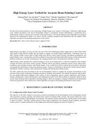
An example of a two-dimensional simulation of a cosmic<br />
particle ionizing charge in a MOSFET transistor. The<br />
simulation code allows researchers to track how ionized<br />
charge moves through a semiconductor structure.<br />
NPS Research page 15<br />
<strong>October</strong> <strong>2000</strong>