

VHDL Made Easy! - Xilinx
VHDL Made Easy! - Xilinx
VHDL Made Easy! - Xilinx
- TAGS
- vhdl
- xilinx
- www.xilinx.com

Create successful ePaper yourself
Turn your PDF publications into a flip-book with our unique Google optimized e-Paper software.
XCELL Issue 21<br />
Second Quarter 1996<br />
T H E Q U A R T E R L Y J O U R N A L F O R X I L I N X P R O G R A M M A B L E L O G I C U S E R S<br />
The Programmable<br />
Logic Company SM<br />
Inside This Issue:<br />
GENERAL<br />
Fawcett: PLDs, Pins, PCBs (part 2) ...........2<br />
Guest Editorial .......................................... 3<br />
Customer Success Story ........................ 6-7<br />
1996 Data Book .......................................7<br />
University Workshops .............................. 8<br />
Training Update .......................................9<br />
Fiscal Year Financial Results .....................9<br />
New Product Literature ......................... 10<br />
Upcoming Events .................................. 10<br />
Development Systems Chart ................. 11<br />
Component Availability Chart .......... 12-13<br />
Alliance Program Charts .................. 14-16<br />
Programming Support Charts ........... 17-19<br />
PRODUCTS<br />
XC9500 Product Life Cycle .............. 20-21<br />
DEVELOPMENT SYSTEMS<br />
Foundation Series ............................. 22-23<br />
XACT-CPLD Introduced ........................ 24<br />
XACTstep 6.0.1 Software Update ......... 25<br />
HINTS & ISSUES<br />
Using OrCAD Capture and Simulate 26-28<br />
Foundation on a Network ..................... 29<br />
Viewlogic’s Workview Office ........... 30-31<br />
HDL Synthesis and Clock Enables .... 32-34<br />
Ten-Digit Synchronous BCD Counter ... 35<br />
Structured Floorplanning .................. 36-39<br />
Minimum Delays .............................. 40-41<br />
Visit FPGA Newsgroup ......................... 41<br />
Advanced Carry-Logic Techniques ... 42-44<br />
PCI-Based Reconfigurable Computers .. 45<br />
Questions & Answers ....................... 46-47<br />
Technical Support Resources ................ 47<br />
Fax Response Form ............................... 48<br />
R<br />
PRODUCT INFORMATION<br />
Advanced Carry<br />
Logic Techniques<br />
The XC4000 FPGA’s carry logic<br />
can be used for lots more than<br />
adders and counters...<br />
See Page 42<br />
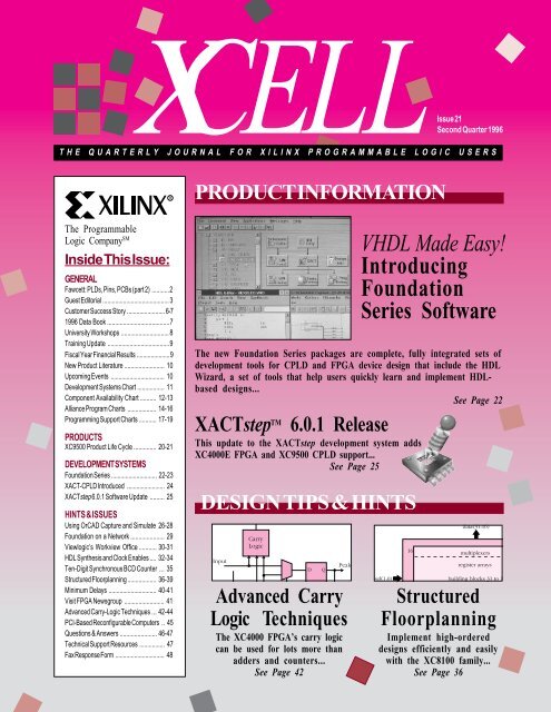
<strong>VHDL</strong> <strong>Made</strong> <strong>Easy</strong>!<br />
Introducing<br />
Foundation<br />
Series Software<br />
The new Foundation Series packages are complete, fully integrated sets of<br />
development tools for CPLD and FPGA device design that include the HDL<br />
Wizard, a set of tools that help users quickly learn and implement HDLbased<br />
designs...<br />
See Page 22<br />
XACTstep TM 6.0.1 Release<br />
This update to the XACTstep development system adds<br />
XC4000E FPGA and XC9500 CPLD support...<br />
See Page 25<br />
DESIGN TIPS & HINTS<br />
Structured<br />
Floorplanning<br />
Implement high-ordered<br />
designs efficiently and easily<br />
with the XC8100 family...<br />
See Page 36
2<br />
XCELL<br />
Please direct all inquiries,<br />
comments and submissions to:<br />
Editor: Bradly Fawcett<br />
<strong>Xilinx</strong>, Inc.<br />
2100 Logic Drive<br />
San Jose, CA 95124<br />
Phone: 408-879-5097<br />
FAX: 408-879-4676<br />
E-Mail: brad.fawcett@xilinx.com<br />
©1996 <strong>Xilinx</strong> Inc.<br />
All rights reserved.<br />
Part 2 of 2<br />
XCELL is published quarterly for<br />
customers of <strong>Xilinx</strong>, Inc. <strong>Xilinx</strong>, the<br />
<strong>Xilinx</strong> logo and XACT are registered<br />
trademarks; all XC-designated<br />
products, UIM, HardWire, Foundation<br />
Series, HDL Wizard, TrueMap,<br />
XACTstep and XACT-Performance<br />
are trademarks; and “The Programmable<br />
Logic Company” is a service<br />
mark of <strong>Xilinx</strong>, Inc. All other trademarks<br />
are the property of their<br />
respective owners.<br />
R<br />
○ ○ ○ ○ ○ ○ ○ ○ ○ ○ ○ ○ ○ ○ ○ ○ ○ ○ ○ ○ ○ ○ ○ ○ ○ ○ ○ ○ ○ ○ ○ ○ ○ ○ ○ ○ ○ ○ ○ ○ ○ ○ ○ ○ ○ ○ ○ ○ ○ ○ ○ ○ ○ ○ ○ ○ ○ ○ ○ ○ ○ ○ ○ ○ ○ ○ ○ ○ ○ ○ ○ ○ ○ ○ ○ ○ ○ ○ ○ ○ ○ ○ ○ ○ ○ ○<br />
FROM THE FAWCETT<br />
PLDs, Pins and PCBs (part 2)<br />
Part 1 of this article (XCELL 20, page<br />
2) discussed the inevitability of design<br />
changes during all stages of an electronic<br />
system’s lifecycle. Changes can occur as a<br />
result of the debugging<br />
and testing of the initial<br />
design, due to specification<br />
changes during the<br />
design, or even to add<br />
features to a mature<br />
product to extend that<br />
product’s life.<br />
An important benefit<br />
of user-programmable<br />
logic is tolerance of<br />
change; with PLDs, design changes can be<br />
implemented quickly and easily. However,<br />
printed circuit board (PCB) designs are not<br />
as easy to change, typically requiring new<br />
drawings (masks) and the manufacturing<br />
of new prototypes, with all the associated<br />
expenses and delays. Thus, to garner all<br />
the benefits of the<br />
flexibility of pro-<br />
grammable logic,<br />
programmable<br />
logic device architectures<br />
should<br />
isolate the PCB<br />
design from logic<br />
changes that occur<br />
within the PLD<br />
device. Device<br />
architectures should do this in two ways<br />
— by supporting pin-locking and with<br />
footprint compatibility.<br />
Pin-locking — that is, for signals<br />
entering and leaving a PLD, maintaining<br />
the pin locations during design changes<br />
internal to the PLD — was discussed at<br />
length in part 1. Support for pin-locking is<br />
a key feature of the latest generations of<br />
<strong>Xilinx</strong> CPLDs and FPGAs.<br />
By BRADLY FAWCETT ◆ Editor<br />
❝footprint<br />
compatibility maximizes<br />
PLD design flexibility, and<br />
has been incorporated in<br />
all <strong>Xilinx</strong> components since<br />
the XC2000 family❞<br />
Equally important, footprint compatibility<br />
maximizes PLD design flexibility,<br />
and has been incorporated in all <strong>Xilinx</strong><br />
components since the XC2000 family —<br />
the world’s first FPGA! Footprint compatibility<br />
refers to the availability of PLDs of<br />
various gate densities with the same<br />
package and with an identical pinout. With<br />
a range of footprint-compatible devices<br />
available, users may migrate a given PLD<br />
design to a higher- or lower-density device<br />
without changing the printed circuit board.<br />
Footprints in the Silicon<br />
There are several scenarios where a<br />
common device footprint provides a significant<br />
advantage. The most prevalent of<br />
these is when a design is being modified<br />
to add features without changing the<br />
pinout requirements, and, as a result, the<br />
design grows to exceed the gate density of<br />
the PLD device that was initially selected.<br />
By moving the<br />
design to a foot-<br />
print-compatible<br />
device with higher<br />
capacity, a re-layout<br />
of the printed<br />
circuit board is<br />
avoided, saving<br />
both time and<br />
money.<br />
On the other<br />
hand, a design can be initially prototyped<br />
in a larger device than needed, to allow<br />
room for expansion and experimentation.<br />
Once the design is fixed, it can be<br />
migrated to a smaller, less-expensive<br />
device in the same package as a cost<br />
reduction. Again, footprint compatibility<br />
between the devices avoids changes to the<br />
printed circuit board. (There is, however,<br />
Continued on page 5
GUEST EDITORIAL<br />
The First Ten Weeks<br />
By WILLEM ROELANDTS ◆ Chief Executive Officer<br />
It is a pleasure to address you after being in my new position for ten weeks.<br />
I feel even better today about my decision to join <strong>Xilinx</strong> than I felt when<br />
I started, now that I have a better understanding of the company and its<br />
products. During the past ten weeks I have spent most of my time meeting<br />
with the <strong>Xilinx</strong> people, our foundry partners, our sales and distribution organizations,<br />
our shareholders and our customers. In general, I am very pleased<br />
with the feedback and inputs that I have received.<br />
I have found that <strong>Xilinx</strong> people are very capable, technically competent<br />
(after all, <strong>Xilinx</strong> did invent FPGA technology), and very motivated.<br />
The relationship between <strong>Xilinx</strong> and our foundry IC partners is both<br />
excellent and enduring. Due to strong teamwork, it has withstood the<br />
inevitable ups and downs of the IC business.<br />
The quality of our independent sales organization is very strong. We have<br />
had long-standing relationships with them and they are very familiar with our<br />
products. Some have invested in their own Field Application Engineers (FAEs),<br />
in order to serve our customers better.<br />
Our customers are pleased with our products. They like the time-to-market<br />
advantages of using FPGAs and CPLDs in design and production, and our standard<br />
parts simplify their production and inventory management. Our users have also<br />
pointed out some issues and opportunities, including on-time delivery, the importance<br />
of software tools and the continuing need for bigger and faster chips.<br />
During this time I also have reflected on our strategic directions. I can assure<br />
you that the major components of this highly successful strategy will not<br />
change. We will continue to:<br />
• Focus on FPGA technology by aggressively increasing size and performance.<br />
The XC4000EX family will reach 125,000 gates in 1997. Our<br />
XC5000 family is an excellent solution for the low-end FPGA market.<br />
The XC8100 family of one-time-programmable FPGAs provides other<br />
unique features.<br />
• Add technologies for specific customer requirements. The very successful<br />
XC9500 family uses a CPLD architecture, but adds in-system<br />
programmability (ISP), a feature highly appreciated by our users.<br />
• Develop reconfigurable logic, which is the ability to dynamically<br />
change the logic configuration of the FPGA during the operation of the<br />
device. This technology promises to change the way logic is designed. It is<br />
an area in which <strong>Xilinx</strong> has done a lot of work and I intend to aggressively<br />
continue the effort.<br />
• Use outside foundries for our wafer processing. It provides the best<br />
flexibility and enables us to provide our customers a stable flow of high<br />
quality products.<br />
Continued on the next page<br />
○ ○ ○ ○ ○ ○ ○ ○ ○ ○ ○ ○ ○ ○ ○ ○ ○ ○ ○ ○ ○ ○ ○ ○ ○ ○ ○ ○ ○ ○ ○ ○ ○ ○ ○ ○ ○ ○ ○ ○ ○ ○ ○ ○ ○ ○ ○ ○ ○ ○ ○ ○ ○ ○ ○ ○ ○ ○ ○ ○ ○ ○ ○ ○ ○ ○ ○ ○ ○ ○ ○ ○ ○ ○ ○ ○ ○ ○ ○ ○ ○ ○ ○ ○ ○ ○<br />
❝I can assure you<br />
that the major components<br />
of this highly successful<br />
strategy will not change.❞<br />
R<br />
3
4<br />
GUEST EDITORIAL<br />
Continued from the previous page<br />
• Work with independent sales organizations,<br />
but provide them with technical<br />
resources for training and support.<br />
• Use the six sigma defect rate standard<br />
as our norm for product quality.<br />
In order to guarantee the quality of our<br />
products, we will continue to do most<br />
product testing in-house.<br />
• Provide technical support that is<br />
second-to-none in the industry. The<br />
ability to contact experts quickly is<br />
critical to maintaining the productivity<br />
of our users.<br />
❝There is no doubt in my mind<br />
that software has to be a core competency<br />
of <strong>Xilinx</strong>; it is as important as our ability<br />
to design FPGA chips.❞<br />
There are some changes or refocusing<br />
of strategic components that I feel<br />
will make <strong>Xilinx</strong> even more successful.<br />
They include:<br />
The importance of software<br />
There is no doubt in my mind that<br />
software has to be a core competency of<br />
<strong>Xilinx</strong>; it is as important as our ability to<br />
design FPGA chips. That’s why we acquired<br />
NeoCAD. I believe we have the<br />
right people and now we are going to<br />
execute. Our objective is to be the best in<br />
the industry, and I intend to give this my<br />
personal attention. You have already seen<br />
some of the results with the introduction<br />
of the XACTstepTM 6.0/5.2 release, the<br />
Japanese version of this product, and the<br />
new FoundationTM release — a fully-integrated,<br />
“shrink-wrap” package for the PC<br />
platform. Foundation software packages<br />
offer the best functionality in their price<br />
class (starting at less that $500), and are<br />
complete software sets delivered from<br />
<strong>Xilinx</strong>! This is only the beginning; more<br />
new capabilities and performance improvements<br />
will be introduced this year.<br />
The opportunity of logistics<br />
The IC industry goes through cycles of<br />
feast and famine, and last year we grew<br />
more than expected, causing us to sometimes<br />
miss our delivery schedules (although<br />
our record was better than most).<br />
I believe that with better planning of the<br />
supply chain, better management of the<br />
distribution process, shorter manufacturing<br />
cycles and more aggressive use of<br />
information technology, we should be<br />
able to do a better job and meet 100% of<br />
our delivery commitments.<br />
Design paradigm change<br />
With the densities of our largest FPGAs<br />
exceeding 100,000 gates, our users will no<br />
longer be able to design logic functions<br />
one gate at a time. In response, we are<br />
moving to a new paradigm. <strong>Xilinx</strong> is<br />
creating libraries of specific functions in<br />
software that will be tested and guaranteed<br />
— we call these LogiCore TM modules.<br />
We envision a design process where the<br />
designer selects the needed functions,<br />
adds the application’s specific logic, and<br />
lets the software put it all together. This<br />
methodology will dramatically reduce the<br />
time required to design complex logic<br />
functions, improving time-to-market and<br />
the efficiency of our users. Of course, the<br />
complete implementation of this vision<br />
will take some time. The first LogiCore<br />
product, the PCI module, has proven this<br />
concept and has been tremendously successful.<br />
We are going to aggressively<br />
pursue this strategy.<br />
So there you have it — an overview of<br />
my thinking after 10 weeks on the job. I<br />
will continue to keep you informed of the<br />
progress we are making on the execution<br />
of our strategy. ◆
THE FAWCETT<br />
Continued from page 2<br />
one caveat to consider when migrating a<br />
design from a larger to a smaller PLD<br />
device. For some smaller devices, the package<br />
may have more physical pins than<br />
there are input/output pads on the device.<br />
Thus, some package pins may be left unconnected.<br />
A larger device in the same<br />
family may have more I/O pads on the die<br />
and, therefore, have connections to all the<br />
pins of the given package. Thus, if migration<br />
to a smaller part is anticipated, the<br />
initial design in the larger device should<br />
avoid using those pin locations that are not<br />
connected in the smaller device.)<br />
In other words, footprint compatibility<br />
lessens any risks associated with<br />
the initial device selection, which often<br />
must be based on a rough estimate of the<br />
design’s requirements. If the selected<br />
device turns out to be too small, the<br />
design is migrated to a larger device. If<br />
the selected device is too big, the design<br />
can be moved to a smaller device. In<br />
either case, potentially expensive and<br />
time-consuming changes to the PCB are<br />
not necessary.<br />
Footprint-compatible devices also<br />
provide the user with more inventory<br />
flexibility. Devices that are on-hand can<br />
be used for prototyping or initial production,<br />
and the design can then be migrated<br />
to a footprint-compatible device for quantity<br />
production. If a sudden demand “upside”<br />
should develop, users have the<br />
option to move to a larger device in the<br />
same family or a similar-sized device from<br />
another footprint-compatible family.<br />
Compatible From the Start<br />
Recognizing these benefits, <strong>Xilinx</strong><br />
always has maintained footprint compatibility<br />
within component product families<br />
and subfamilies whenever multiple<br />
devices share common packages. For<br />
example, the XC3030 and XC3042 devices<br />
share a common footprint in the PC84,<br />
TQ100, and VQ100 packages. That same<br />
footprint is maintained in the equivalent<br />
density members of the XC3000A, XC3100,<br />
XC3100A, and XC3000L sub-families. (The<br />
only exceptions are the XC3000 series and<br />
its derivatives in the PC 84 package, where<br />
some of the larger devices need two additional<br />
GND and V CC connections, and in<br />
the PQ208 package, where the XC3090 and<br />
XC3195 devices do not have compatible<br />
footprints.)<br />
Cross-family compatibility began with<br />
the XC4000 series of FPGAs and includes<br />
the XC5000 series and the XC8100 series<br />
— all sharing common footprints in common<br />
packages. This provides designers<br />
with many options. For example, as<br />
reported in XCELL 19, VTEL Corp., a<br />
manufacturer of video teleconferencing<br />
systems and one of the first adopters of<br />
the XC5000 family, prototyped their<br />
designs in XC4000 series FPGAs while<br />
awaiting the availability of XC5000<br />
components and development tools.<br />
The resulting designs were easily<br />
migrated to lower-cost, footprintcompatible<br />
XC5000 devices for production<br />
systems. In a similar scenario,<br />
a designer could exploit the re-usable<br />
nature of the SRAM-based XC4000 or<br />
XC5000 FPGAs for debug and<br />
prototyping purposes, and then<br />
switch to the one-time-programmable<br />
XC8100 family for production.<br />
Designers should avoid getting<br />
locked into programmable logic solutions<br />
that offer little flexibility in pin assignments<br />
and device selection. <strong>Xilinx</strong><br />
CPLDs and FPGAs offer the best pinlocking<br />
capabilities in the industry, and<br />
the broadest spectrum of footprint-compatible<br />
devices. These features allow users<br />
to avoid modifications to printed circuit<br />
board designs, thereby accelerating timeto-market<br />
and accommodating the inevitable<br />
design changes that occur throughout<br />
a product’s total life cycle. ◆<br />
❝Designers<br />
should avoid getting<br />
locked into<br />
programmable logic<br />
solutions that offer<br />
little flexibility in pin<br />
assignments and<br />
device selection.❞<br />
5
6<br />
CUSTOMER SUCCESS STORY<br />
FPGAs Go “Down Under” in an<br />
Engineers at communications equipment<br />
specialist Tennyson Technologies<br />
(Notting Hill, Victoria, Australia) are experienced<br />
users of <strong>Xilinx</strong> XC3000 and<br />
XC4000 series FPGAs. Thus, when a new<br />
project created a need for high integration<br />
levels, design flexibility, and a fast timeto-market,<br />
all at a reasonable cost, it was<br />
no surprise that they turned to the latest<br />
<strong>Xilinx</strong> FPGA<br />
technology —<br />
the XC5000<br />
series. In<br />
Tennyson’s<br />
new<br />
MicroAccess<br />
PCTA terminal<br />
adapter card,<br />
both bus interface<br />
and communication<br />
control functions<br />
are integrated<br />
into a<br />
single XC5206-<br />
6 FPGA device.<br />
The Micro-<br />
Access system<br />
includes a<br />
plug-in card for PC systems and the<br />
accompanying software. It allows any PC<br />
or PC LAN to automatically make connections<br />
to off-site systems; the connection<br />
can be made to last only as long as information<br />
is being exchanged, much like a<br />
telephone call. With support for voice<br />
and data transfers, the MicroAccess<br />
system permits connectivity through ISDN,<br />
regular telephone line or X.25 services.<br />
The logic functions implemented in the<br />
FPGA device include the ISA-bus interface,<br />
FIFO control, communications<br />
control, V110 rate adaptation, data com-<br />
pression/decompression, and other glue<br />
logic. The bus interface supports plugand-play<br />
capability and accounts for<br />
about one-half of the logic in the FPGA.<br />
The bulk of the communications control<br />
logic consists of the counters used to<br />
assemble and synchronize the frames of<br />
data. About 75% of the available CLBs are<br />
used in this design, as well as most of the<br />
I/O pins available on the PQ208 package.<br />
While any of several FPGA families<br />
could have provided the required density<br />
and functionality, Tennyson’s engineers<br />
were attracted to the XC5000<br />
architecture’s VersaRing TM feature, in<br />
which extra routing channels around the<br />
perimeter of the array increase the flexibility<br />
of I/O connections. In order to<br />
meet the time-to-market goals, the designers<br />
realized that the printed circuit board<br />
(PCB) would need to be designed in<br />
parallel with the system’s logic. Thus, the<br />
pinout for the XC5206 FPGA was fixed<br />
prior to the design of its internal logic.<br />
Through each design iteration, the<br />
VersaRing concept held true; changes<br />
to the FPGA design did not force any<br />
changes to the original PCB layout.<br />
The flexibility provided by the SRAMbased<br />
FPGA was key to the successful<br />
design of the system. For example, the<br />
board was originally intended to support<br />
a 16-bit ISA bus interface only, but the<br />
specification was later changed to require<br />
support for both 8-bit XT and 16-bit AT<br />
systems. Since the entire bus interface is<br />
implemented in the FPGA, this requirement<br />
was accommodated, without requiring<br />
changes to the PCB layout as a result.<br />
Taking advantage of the in-systemprogrammable<br />
FPGA technology, the<br />
MicroAccess board has been designed in<br />
anticipation of future field upgrades. New
ISDN Terminal Adapter<br />
software (stored in Flash memory on the<br />
board) and new FPGA configuration programs<br />
can be downloaded to units in the<br />
field via an ISDN interface. In fact, one set<br />
of FPGA configuration programs has been<br />
dubbed the “Emergency <strong>Xilinx</strong>” diagnostic<br />
mode; this configuration runs just the<br />
ISDN channel, allowing for the downloading<br />
of new software and configuration<br />
bitstreams to the system.<br />
Tennyson Technology’s development<br />
environment is PC-based, and includes<br />
Viewlogic System’s schematic editor and<br />
simulator, as well as the <strong>Xilinx</strong> XACT ®<br />
development system. XACT-Performance TM<br />
time specifications and some floorplanning<br />
1996 Data Book Available Soon<br />
The 1996 <strong>Xilinx</strong> Programmable Logic<br />
Data Book will be available this summer. It<br />
will contain data sheets and product specifications<br />
describing <strong>Xilinx</strong> component and<br />
development system products, including the<br />
latest information on the new XC4000E,<br />
XC4000EX , XC6200, XC8100 and XC9500<br />
device families. Other included device families<br />
described are the XC7200A and XC7300<br />
CPLD families, the XC3000A, XC3000L,<br />
XC3100A, XC3100L, XC4000L, XC4000XL and<br />
XC5200 FPGA families, and the XC1700<br />
family of Serial PROMs.<br />
The product specifications for the<br />
XC2000, XC3000, XC3100, XC4000,<br />
XC4000A, XC4000D, and XC4000H FPGA<br />
families are not included. These products<br />
are still available; however, we recommend<br />
using the products in the data book for new<br />
designs because they offer better performance<br />
at lower cost than the older tech-<br />
of the FPGA placement were used to meet<br />
the required 33 MHz system clock rate, a<br />
fairly aggressive goal when using the -6<br />
speed grade. Both the Viewsim simulator<br />
and the X-Delay timing calculator were<br />
used to verify the functionality and timing<br />
of the FPGA design.<br />
With the aid of <strong>Xilinx</strong> FPGAs, Tennyson<br />
Technology’s MicroAccess system is allowing<br />
some of Australia’s leading organizations<br />
to combine telephone and data traffic<br />
into single services, providing for better<br />
communications with branch offices and<br />
other remote locations while reducing<br />
overall communication costs. ◆<br />
nologies. Product specifications for the<br />
older products are available at WebLINX,<br />
the <strong>Xilinx</strong> site on the World Wide Web<br />
(www.xilinx.com), or through your local<br />
<strong>Xilinx</strong> sales representative.<br />
The military/highreliability<br />
and HardWire TM<br />
product lines are overviewed<br />
in the 1996 edition,<br />
but will retain their<br />
own, separate detailed product<br />
specification literature.<br />
While the book provides detailed,<br />
easy-to-access information about <strong>Xilinx</strong><br />
products, as a book, it can only offer a<br />
“snapshot” of <strong>Xilinx</strong> products in early<br />
1996. Inquire with your sales representative,<br />
WebLINX or this journal for the<br />
latest information on new devices,<br />
speed grades, package types and<br />
development systems. ◆<br />
7
8<br />
<strong>Xilinx</strong> Hosts<br />
University<br />
Workshops<br />
WORKSHOP SCHEDULE<br />
UNITED STATES<br />
If you are a university professor who<br />
would like to incorporate programmable<br />
logic technology into your engineering<br />
curriculum, get started by attending a<br />
<strong>Xilinx</strong> University Workshop. <strong>Xilinx</strong> technology<br />
has been used in many engineering<br />
courses, including beginning and<br />
advanced digital design, processor architecture,<br />
digital signal processing, VLSI<br />
design, data communications and various<br />
project-oriented laboratory courses.<br />
This summer, <strong>Xilinx</strong> will be hosting<br />
four workshops in the United States and<br />
two in Asia. These workshops provide a<br />
thorough introduction to programmable<br />
logic technology, and discuss how to<br />
integrate the technology into first-year<br />
through fifth-year university courses. The<br />
workshops are taught by a team of <strong>Xilinx</strong><br />
training professionals and local professors<br />
with experience at using programmable<br />
logic in their own coursework. Technolo-<br />
<strong>Xilinx</strong>/Washington State University Workshop<br />
Richland, WA ◆ June 24 - 26<br />
In addition to the basic course material, Dr. Donald<br />
Hung will discuss his first-hand experiences in developing<br />
courses that use programmable logic.<br />
<strong>Xilinx</strong>/Cornell University<br />
Reconfigurable Computing Workshop<br />
Ithaca, NY ◆ July 10 -12<br />
This will be our first hands-on workshop devoted to the<br />
topic of reconfigurable computing with FPGAs. Targeted<br />
at educators who are familiar with reprogrammable logic<br />
and are very interested in the concept of dynamically<br />
reconfigurable computing, this workshop will condense<br />
the basic material and focus on this new and promising<br />
ASIAN SCHEDULE<br />
Workshops are planned for the week of August 19 in<br />
China, and the week of August 26 in Taiwan. Further<br />
details were not available at the time of this printing.<br />
gies covered at the workshops include<br />
field programmable gate arrays (FPGAs),<br />
complex programmable logic devices<br />
(CPLDs), and dynamically reconfigurable<br />
logic. Although most workshops will cover<br />
the same basic material, some will have<br />
special themes, as described below.<br />
Hands-on labs using PC-based development<br />
tools are included in each workshop.<br />
These three-day workshops are available<br />
free of charge to professors and instructors.<br />
However, due to the popularity<br />
of the workshops, attendance is limited to<br />
two people from each university or college.<br />
Seating and hotel rooms at each<br />
workshop are limited, so early registration<br />
is advised.<br />
To register, contact Jason Feinsmith,<br />
<strong>Xilinx</strong> University Program Manager, at<br />
408-879-4961 or e-mail xup@xilinx.com<br />
or visit www.xilinx.com/programs/univ.htm<br />
for information. ◆<br />
area of study. Several researchers will be present to discuss<br />
their work.<br />
<strong>Xilinx</strong>/Massachusetts Institute<br />
of Technology Workshop<br />
Boston, MA ◆ July 15 - 17<br />
For those particularly interested in computer architectures,<br />
this workshop will include a look at MIT’s newlycreated<br />
computer structures curriculum based on <strong>Xilinx</strong><br />
devices and the “electric legos” concept.<br />
<strong>Xilinx</strong>/Oakland University Workshop<br />
Detroit, MI ◆ July 24 - 26<br />
Dr. Subra Ganesan will discuss his work in using FPGAs<br />
in digital signal processing applications at this workshop.<br />
For up-to-date information, visit<br />
www.xilinx.com/programs/univ.htm<br />
on the World Wide Web. ◆
FINANCIAL RESULTS<br />
Fiscal 1996: Another Record Year<br />
As in every year since <strong>Xilinx</strong> was<br />
founded, the company again achieved<br />
record revenues in fiscal year 1996 (April<br />
1995-March 1996). Fiscal 1996 revenues<br />
totaled $560.8 million, an increase of 58%<br />
over fiscal 1995, reflecting the continuing<br />
strength of our product line and expansion<br />
of the programmable logic market.<br />
Key accomplishments of fiscal 1996<br />
include the following:<br />
• The flagship XC4000 series products<br />
contributed revenues of over $250<br />
million, more than doubling the<br />
revenue of the prior year.<br />
• International revenues grew by more<br />
than 80% to $198 million.<br />
• <strong>Xilinx</strong> Ireland, our first wholly-owned<br />
manufacturing site outside of the U.S.,<br />
became fully operational.<br />
• The merger with NeoCAD Corp. was<br />
completed, providing access to powerful<br />
new software solutions.<br />
• Access to leading-edge process technology<br />
was enhanced with a 25%<br />
equity investment in an 8-inch wafer<br />
fabrication facility in a joint venture<br />
with United Microelectronics Corp.<br />
• Our commitment to product development<br />
was exemplified by research and<br />
development spending of approximately<br />
$65 million, 63% more than the<br />
second-largest programmable logic<br />
supplier.<br />
As noted by Willem Roelandts, Chief<br />
Executive Officer, “<strong>Xilinx</strong> is well-positioned<br />
as we enter fiscal 1997. New products<br />
that we introduced in the second half<br />
of fiscal 1996, including the high-performance<br />
XC4000E, the high-density<br />
XC4000EX, and the Flash-based insystem-programmable<br />
XC9500 CPLD<br />
family, should become key revenue<br />
drivers next year. Moreover, all these<br />
silicon products will be supported by a<br />
new, more-powerful, and easier-to-use<br />
software solution. Looking ahead, we<br />
remain optimistic about the overall<br />
growth of programmable logic and our<br />
position within this market.”<br />
Paced by growth in the European<br />
market, revenues for the fourth fiscal<br />
quarter (ending in March) reached a<br />
record $149.7 million, up 37% from the<br />
same quarter one year ago, and 4% from<br />
the immediately previous quarter.<br />
Founded in 1984, <strong>Xilinx</strong> is the<br />
world’s largest supplier of programmable<br />
logic devices. <strong>Xilinx</strong> stock is<br />
traded on the NASDAQ exchange under<br />
stock symbol XLNX. ◆<br />
TRAINING UPDATE<br />
Advanced Training Available<br />
The advanced training course is again available at <strong>Xilinx</strong> headquarters<br />
in San Jose, California. The session focuses on features of<br />
the <strong>Xilinx</strong> devices and development system that allow experienced<br />
users to create more efficient designs.<br />
Advanced training will be useful for anyone “pushing the envelope”<br />
in terms of the speed and density of <strong>Xilinx</strong> FPGA products,<br />
especially the XC4000 family devices. The primary focus is on<br />
floorplanning and the use of the new graphical FloorplannerTM .<br />
Classes are scheduled regularly at <strong>Xilinx</strong> headquarters starting in<br />
May. The class is open to all in-warranty <strong>Xilinx</strong> customers at no<br />
charge. Previous experience with the <strong>Xilinx</strong> products is a prerequisite<br />
for the advanced training course.<br />
For more information or to register, visit WebLINX<br />
(www.xilinx.com) on the World Wide Web, call <strong>Xilinx</strong> Training<br />
at 408-879-5090, or e-mail to customer.training@xilinx.com. ◆<br />
9
10<br />
New Product<br />
Literature<br />
UPCOMING EVENTS<br />
Learn about the newest <strong>Xilinx</strong> products and services through our extensive library of<br />
product literature. The most recent pieces are listed below. To order or to obtain a complete<br />
list of all available literature, please contact your local <strong>Xilinx</strong> sales representative. ◆<br />
TITLE DESCRIPTION NUMBER<br />
FPGAs<br />
XC4000 to XC4000E Conversion Guide Technical Data #0010295-01<br />
Interfacing between 5-V and 3.3-V Technical Data #0010296-01<br />
Efficient Shift Registers Technical Data #0010298-01<br />
CPLDs<br />
XC9500 Quick Reference Guide Features & Benefits #0010408-01<br />
Software<br />
XACTstep 5.2 Sell Sheet Features & Benefits #0010289-01<br />
<strong>Xilinx</strong> Foundation Series Sell Sheet Features & Benefits #0010292-01<br />
Other<br />
1996 Training Brochure #0010134-05<br />
Literature Packet: DSP Technical Data Packet #2<br />
Literature Packet: RADD (Reconfigurable Architectures) Technical Data Packet #15<br />
Look for <strong>Xilinx</strong> technical papers and/or product exhibits at these upcoming industry<br />
forums. For further information about any of these conferences, please contact Kathleen<br />
Pizzo (Tel: 408-879-5377 FAX: 408-879-4676). ◆<br />
Design Automation Conference (DAC)<br />
June 3-7<br />
Las Vegas, Nevada<br />
Intertronic<br />
June 4-7<br />
Paris, France<br />
DSP Roadshow<br />
June 5-6<br />
Manchester, UK<br />
DSP<br />
Scandinavia<br />
June 18-19<br />
Copenhagen,<br />
Denmark<br />
International Conference on Application<br />
Specific Systems, Architectures,<br />
and Processors<br />
Aug. 19-21<br />
Chicago, Illinois<br />
Electronic Design Automation and Test<br />
Conference (EDA&T)<br />
Sept. 5 -6 , Beijing, China<br />
Sept. 9-10, Seoul, Korea<br />
Sept. 12-13, Hsinchu, Taiwan<br />
DSP Roadshow<br />
Sept. 25-26<br />
London, UK<br />
International Workshop on Field Programmable<br />
Logic and Applications<br />
Sept. 23-25<br />
Darmstadt, Germany
XILINX RELEASED SOFTWARE STATUS - MAY 1996<br />
XILINX PART CURRENT V ERSION BY PLATFORM LAST PREVIOUS<br />
PRODUCT PRODUCT PRODUCT REFERENCE PC1 SN2 HP7 UPDT VERSION COMMENTS<br />
KEY CATEGORY DESCRIPTION FUNCTION NUMBER 6.2 4.1.X 9.01 COMP RELEASE FEATURES<br />
CORE EPLD XC7K, XC9500 Support Core Implementation DS-550-xxx 6.00 5.20 5.20 11/95 5.10 PC update by request only<br />
XABEL-CPLD XC7K, XC9500 Support Entry/Simulation/Core DS-571-PC1 6.10 na 6.01 No key required with version 6.0.1<br />
N XACT-CPLD XC7K, XC9500 Support Core + I/F DS-560-xxx 6.0 6.0 6.0 na na First ship 4/23/96<br />
Mentor 8.4=A.4 I/F and Libraries DS-344-xxx 5.20 5.20 11/95 5.11 No AP1 update<br />
OrCAD I/F and Libraries DS-35-PC1 5.20 11/95 5.10 Support for SDT+, VST+ v1.2<br />
Synopsys I/F and Libraries DS-401-xxx 5.20 5.20 11/95 3.30 Includes XC5200 X-BLOX Support<br />
Viewlogic PROcapture I/F and Libraries DS-390-PC1 6.00 11/95 5.11 Includes PRO Series 6.1<br />
Viewlogic PROsim I/F and Libraries DS-290-PC1 6.00 11/95 5.11 Includes PRO Series 6.1<br />
Viewlogic I/F and Libraries DS-391-xxx 6.00 5.20 5.20 11/95 5.11<br />
XABEL Entry,Simulation,Lib, Optimizer DS-371-xxx 5.20 5.20 5.20 11/95 5.10 Now available on HP7<br />
XBLOX Module Generator & Optimizer DS-380-xxx 5.20 5.20 5.20 11/95 5.10<br />
E Verilog 2K,3K,4K,7K Libraries Models & XNF Translator ES-VERILOG-xxx 1.00 1.00 na na Sun and HP<br />
SILICON SUPPORT<br />
2K 3K 4K 5K 7K 8K 9K<br />
Cadence X X X X X DS-CDN-STD-xxx 5.20 5.20 11/95 5.11<br />
XC8000 X DS-8000-STD-xxx 1.10 1.10 1.10 na na Incl sch and sim libraries<br />
XC8000 X DS-8000-EXT-xxx 1.10 1.10 1.10 08/95 1.00 Incl sch, sim, and synth libraries<br />
Mentor X X X X X DS-MN8-STD-xxx 5.20 5.20 11/95 5.11 No AP1 update<br />
Mentor X X X X X DS-MN8-ADV-xxx 7.00 7.00 na na<br />
U OrCAD X X X X X DS-OR-BAS-PC1 6.00 11/95 5.11 Update by request only<br />
OrCAD X X X X X DS-OR-STD-PC1 6.00 11/95 5.11<br />
Synopsys X/E X X X DS-SY-STD-xxx 5.20 5.20 11/95 5.12 Includes DS-401 v5.2<br />
Synopsys X/E X X X DS-SY-ADV-xxx 7.00 7.00 na na Includes DS-401 v5.2<br />
U Viewlogic X X X X X DS-VL-BAS-PC1 6.00 11/95 5.11 Update by request only<br />
Viewlogic X X X X X DS-VL-STD-xxx 6.00 6.00 6.00 11/95 5.11<br />
Viewlogic X X X X X DS-VL-ADV-xxx 7.00 7.00 7.00 na na<br />
Viewlogic/S X X X X X DS-VLS-BAS-PC1 6.00 11/95 5.11 Includes PROSeries 6.1<br />
Viewlogic/S X X X X X DS-VLS-STD-PC1 6.00 11/95 5.11 Includes PROSeries 6.1<br />
Viewlogic/S X X X X X DS-VLS-EXT-PC1 6.00 11/95 5.11 Incl PROSeries 6.1/PROsynth 5.02X<br />
Viewllogic/S X X X X X DS-VLS-ADV-PC1 7.00 na na<br />
U 3rd Party Alliance X X X X X DS-3PA-BAS-xxx 6.00 na na<br />
3rd Party Alliance X X X X X DS-3PA-STD-xxx 6.00 5.20 5.20 na 5.10 Includes 502/550/380<br />
3rd Party Alliance X X X X X DS-3PA-ADV-xxx 7.00 7.00 7.00 na na Includes 502/550/380 & Foundry<br />
Foundation Series X X X X X SCH DS-FND-BAS-PC1 6.00 na na New Aldec software v2.2: 1st ship 3/15/96<br />
Foundation Series X X X X X SCH DS-FND-BSV-PC1 6.00 na na New Aldec software v2.2: 1st ship 3/15/96<br />
Foundation Series X X X X X SCH DS-FND-STD-PC1 6.00 na na New Aldec software v2.2: 1st ship 3/15/96<br />
Foundation Series X X X X X SCH DS-FND-STV-PC1 6.00 na na New Aldec software v2.2: 1st ship 3/15/96<br />
LogiCore - PCI 4KE LC-DI-PCIM-C 1.00 1.00 1.00 na na Req signed lic agreement; 1st ship 3/15/96<br />
N Evaluation X X X X X X X DS-EVAL-XXX-C 1.00 1.00 1.00 na na PC, Sun, HP kits now available<br />
SCH. SIM. SYN. LIB.<br />
PR XC4000E X X PR-MN8-STD- xxx-4E 1.00 1.00 na na By request only; Req In-wnty prod<br />
PR XC4000E X X PR-OR-STD- xxx-4E 1.00 na na By request only; Req In-wnty prod<br />
PR XC4000E <strong>VHDL</strong> <strong>VHDL</strong> PR-SY-STD-xxx-4E 1.00 1.00 na na By request only; Req In-wnty prod<br />
Verilog<br />
PR XC4000E X X PR-VL-STD- xxx-4E 1.00 1.00 1.00 na na By request only; Req In-wnty prod<br />
PR XC4000E X X PR-3PA-STD- xxx-4E 1.00 1.00 1.00 na na By request only; Req In-wnty prod<br />
XILINX INDIVIDUAL PRODUCTS<br />
XILINX PACKAGES<br />
PRE-RELEASE<br />
KEY: N=New Product, E= Engineering Software for in-warranty users by Request Only, U= Update by request only,<br />
PR = Pre-release requiring in-warranty status or Product Marketing apporval<br />
11
12<br />
PINS<br />
44<br />
48<br />
64<br />
68<br />
84<br />
100<br />
120<br />
132<br />
144<br />
156<br />
160<br />
164<br />
175<br />
176<br />
184<br />
191<br />
196<br />
208<br />
223<br />
225<br />
228<br />
240<br />
299<br />
304<br />
352<br />
411<br />
432<br />
499<br />
596<br />
TYPE<br />
CODE<br />
PLASTIC LCC PC44<br />
PLASTIC QFP PQ44<br />
PLASTIC VQFP VQ44<br />
CERAMIC LCC WC44<br />
PLASTIC DIP PD48<br />
PLASTIC VQFP VQ64<br />
PLASTIC LCC PC68<br />
CERAMIC LCC WC68<br />
CERAMIC PGA PG68<br />
PLASTIC LCC PC84<br />
CERAMIC LCC WC84<br />
CERAMIC PGA PG84<br />
CERAMIC QFP CQ100<br />
PLASTIC PQFP PQ100<br />
PLASTIC TQFP TQ100<br />
PLASTIC VQFP VQ100<br />
TOP BRZ. CQFP CB100<br />
CERAMIC PGA PG120<br />
PLASTIC PGA PP132<br />
CERAMIC PGA PG132<br />
PLASTIC TQFP TQ144<br />
CERAMIC PGA PG144<br />
CERAMIC PGA PG156<br />
PLASTIC PQFP PQ160<br />
CERAMIC QFP CQ164<br />
TOP BRZ. CQFP CB164<br />
PLASTIC PGA PP175<br />
CERAMIC PGA PG175<br />
PLASTIC TQFP TQ176<br />
CERAMIC PGA PG184<br />
CERAMIC PGA PG191<br />
TOP BRZ. CQFP CB196<br />
PLASTIC PQFP PQ208<br />
METAL MQFP MQ208<br />
HI-PERF QFP HQ208<br />
CERAMIC PGA PG223<br />
PLASTIC BGA BG225<br />
WINDOWED BGA WB225<br />
TOP BRZ. CQFP CB228<br />
PLASTIC PQFP PQ240<br />
METAL MQFP MQ240<br />
HI-PERF QFP HQ240<br />
CERAMIC PGA PG299<br />
HI-PERF. QFP HQ304<br />
PLASTIC BGA BG352<br />
CERAMIC PGA PG411<br />
PLASTIC BGA BG432<br />
CERAMIC PGA PG499<br />
PLASTIC BGA BG596<br />
COMPONENT AVAILABILITY CHART<br />
XC3020A<br />
XC3030A<br />
XC3042A<br />
XC3064A<br />
XC3090A<br />
XC3020L<br />
XC3030L<br />
XC3042L<br />
XC3064L<br />
XC3090L<br />
XC3142L<br />
XC3190L<br />
XC3120A<br />
XC3130A<br />
XC3142A<br />
XC3164A<br />
XC3190A<br />
XC3195A<br />
XC4003E<br />
XC4005E<br />
XC4006E<br />
XC4008E<br />
XC4010E<br />
XC4013E<br />
XC4020E<br />
XC4025E<br />
XC4028EX<br />
XC4036EX<br />
XC4044EX<br />
XC4052XL<br />
XC4062XL<br />
XC4085XL<br />
XC40125XL<br />
◆ ◆<br />
◆ ◆ ◆<br />
◆◆ ◆◆<br />
◆◆◆◆◆◆◆◆◆◆◆◆◆◆◆◆◆◆◆◆◆◆◆<br />
◆◆◆ ◆◆◆<br />
◆◆◆ ◆◆◆<br />
◆◆<br />
◆◆ ◆◆ ❖ ◆◆<br />
◆ ◆ ◆ ◆<br />
◆◆ ◆◆<br />
◆◆ ◆◆<br />
◆◆❖ ◆◆❖◆◆ ◆◆<br />
◆◆ ◆◆◆<br />
◆ ◆ ◆<br />
◆ ◆ ◆<br />
◆ ◆ ◆<br />
◆ ◆ ◆ ◆<br />
◆ ◆ ◆<br />
◆ = Product currently shipping or planned ❖ = New since last issue of XCELL<br />
◆<br />
◆◆<br />
◆<br />
◆<br />
◆◆<br />
◆◆<br />
◆◆◆◆◆<br />
❖❖<br />
◆◆◆◆◆<br />
◆◆ ◆<br />
◆◆◆<br />
◆◆<br />
◆<br />
◆◆❖◆<br />
◆◆<br />
◆◆◆<br />
◆<br />
◆◆❖<br />
◆◆◆<br />
◆◆<br />
◆◆◆◆
PINS<br />
44<br />
48<br />
64<br />
68<br />
84<br />
100<br />
120<br />
132<br />
144<br />
156<br />
160<br />
164<br />
175<br />
176<br />
184<br />
191<br />
196<br />
208<br />
223<br />
225<br />
228<br />
240<br />
299<br />
304<br />
352<br />
411<br />
432<br />
499<br />
596<br />
TYPE<br />
CODE<br />
PLASTIC LCC PC44<br />
PLASTIC QFP PQ44<br />
PLASTIC VQFP VQ44<br />
CERAMIC LCC WC44<br />
PLASTIC DIP PD48<br />
PLASTIC VQFP VQ64<br />
PLASTIC LCC PC68<br />
CERAMIC LCC WC68<br />
CERAMIC PGA PG68<br />
PLASTIC LCC PC84<br />
CERAMIC LCC WC84<br />
CERAMIC PGA PG84<br />
CERAMIC QFP CQ100<br />
PLASTIC PQFP PQ100<br />
PLASTIC TQFP TQ100<br />
PLASTIC VQFP VQ100<br />
TOP BRZ. CQFP CB100<br />
CERAMIC PGA PG120<br />
PLASTIC PGA PP132<br />
CERAMIC PGA PG132<br />
PLASTIC TQFP TQ144<br />
CERAMIC PGA PG144<br />
CERAMIC PGA PG156<br />
PLASTIC PQFP PQ160<br />
CERAMIC QFP CQ164<br />
TOP BRZ. CQFP CB164<br />
PLASTIC PGA PP175<br />
CERAMIC PGA PG175<br />
PLASTIC TQFP TQ176<br />
CERAMIC PGA PG184<br />
CERAMIC PGA PG191<br />
TOP BRZ. CQFP CB196<br />
PLASTIC PQFP PQ208<br />
METAL MQFP MQ208<br />
HI-PERF QFP HQ208<br />
CERAMIC PGA PG223<br />
PLASTIC BGA BG225<br />
WINDOWED BGA WB225<br />
TOP BRZ. CQFP CB228<br />
PLASTIC PQFP PQ240<br />
METAL MQFP MQ240<br />
HI-PERF QFP HQ240<br />
CERAMIC PGA PG299<br />
HI-PERF. QFP HQ304<br />
PLASTIC BGA BG352<br />
CERAMIC PGA PG411<br />
PLASTIC BGA BG432<br />
CERAMIC PGA PG499<br />
PLASTIC BGA BG596<br />
MAY 1996<br />
XC4005L<br />
XC4010L<br />
XC4013L<br />
XC5202<br />
XC5204<br />
XC5206<br />
XC5210<br />
XC5215<br />
XC8100<br />
XC8101<br />
XC8103<br />
XC8106<br />
XC8109<br />
XC7236A<br />
XC7272A<br />
XC7318<br />
XC7336<br />
XC7336Q<br />
XC7354<br />
XC7372<br />
XC73108<br />
XC73144<br />
XC9536<br />
XC95108<br />
XC95216<br />
◆ ◆ ◆ ◆◆◆◆ ◆<br />
◆◆◆<br />
◆ ◆ ◆<br />
◆ ◆◆◆<br />
◆ ◆ ◆<br />
◆ ◆ ◆<br />
◆◆ ◆◆◆◆ ◆◆◆◆ ◆ ◆◆ ◆<br />
◆ ◆ ◆<br />
◆◆◆<br />
❖❖❖<br />
◆◆◆ ◆◆ ◆<br />
◆<br />
◆◆◆◆<br />
◆<br />
◆◆❖<br />
◆◆◆❖ ◆ ◆ ◆ ◆ ◆<br />
◆ ❖❖<br />
◆<br />
◆◆◆ ◆◆<br />
◆ ◆<br />
◆ ◆ ◆ ◆ ◆ ◆<br />
◆ ◆<br />
◆<br />
◆<br />
◆<br />
❖<br />
13
14<br />
XILINX ALLIANCE - EDA COMPANIES & PRODUCTS - MAY 1996 - 1 OF 2<br />
2K/3K/ XC CPLD XC UNI PLATFORMS<br />
COMPANY NAME PRODUCT NAME VERSION FUNCTION DESIGNKIT 4K 5200 7K9K 8100 LIB PC SUN RS6000 HP7<br />
Aldec Active-CAD 2.0 Schematic Entry & Simulation & HDL Editor Included ✓ ✓ ✓ ✓ ✓ ✓<br />
Cadence Verilog 2.3.2 Simulation <strong>Xilinx</strong> Front End ✓ ✓ 7k ✓ ✓ ✓ ✓ ✓<br />
Concept 2.1 Schematic Entry <strong>Xilinx</strong> Front End ✓ 7k ✓ ✓ ✓ ✓ ✓<br />
FPGA Designer 9504 Topdown FPGA Synthesis Call <strong>Xilinx</strong> ✓ ✓ 7k Q3 ✓ ✓ ✓ ✓<br />
Synergy 2.3 FPGA Synthesis Call <strong>Xilinx</strong> ✓ ✓ 7k ✓ ✓ ✓ ✓ ✓<br />
Composer 4.3.4/4.4 Schematic Entry <strong>Xilinx</strong> Front End ✓ 7k TBD ✓ ✓ ✓ ✓<br />
Mentor Graphics Autologic A.x_F Synthesis <strong>Xilinx</strong> Synthesis Lib. ✓ ✓ 7k ✓ ✓ ✓ ✓ ✓<br />
Design Architect A.x_F Schematic Entry Call <strong>Xilinx</strong> ✓ ✓ 7k ✓ ✓ ✓ ✓ ✓<br />
QuickSim II A.x_F Simulation Call <strong>Xilinx</strong> ✓ ✓ 7k ✓ ✓ ✓ ✓ ✓<br />
OrCAD Simulate (Win) 6.10 Simulation Call <strong>Xilinx</strong> Q3 ✓<br />
VST 386+ (DOS) 1.2 Simulation Call <strong>Xilinx</strong> ✓ 7k ✓ ✓<br />
Capture (Win) 6.11 Schematic Entry Call <strong>Xilinx</strong> ✓ ✓ 7k ✱✓ ✓ ✓<br />
SDT 386+ (DOS) 1.2 Schematic Entry Call <strong>Xilinx</strong> ✓ 7k ✓ ✓<br />
PLD 386+ (DOS) 2.0 Synthesis Call OrCAD ✓ 7k ✓<br />
DIAMOND<br />
Synario Design Automation ABEL 6.2 Synthesis, Simulation XEPLD Fitter 7k,9k ✓ ✓<br />
Synario 2.2 Schematic Entry, Synthesis & Simulation SYN-LCA ✓ ✓ 7k,9k TBD ✓ ✓<br />
Synopsys FPGA Compiler 3.4a Synthesis Call <strong>Xilinx</strong> 3K, 4K ✓ 7k ✓ ✓ ✓ ✓ ✓<br />
VSS 3.4a Simulation Call <strong>Xilinx</strong> ✓ ✓ 7k ✓ ✓ ✓ ✓ ✓<br />
Design Compiler 3.4a Synthesis Call <strong>Xilinx</strong> ✓ ✓ 7k ✓ ✓ ✓ ✓ ✓<br />
Viewlogic WorkView Office 5.5 Schem/Sim/Synth Call <strong>Xilinx</strong> ✓ XACT6 ✓ ✓ ✓ ✓ ✓ ✓ ✓<br />
ProSynthesis 5.02 Synthesis call <strong>Xilinx</strong> ✓ XACT6 7k ✓ ✓ ✓ ✓ ✓ ✓<br />
ProSim 6.1 Simulation, Timing Analysis call <strong>Xilinx</strong> ✓ XACT6 7k ✓ ✓ ✓ ✓ ✓ ✓<br />
ProCapture 6.1 Schematic Entry call <strong>Xilinx</strong> ✓ XACT6 7k ✓ ✓ ✓ ✓ ✓ ✓<br />
Capilano Computing Design Works 3.1 Schematic Entry/Sim XD-1 ✓ ✓ ✓<br />
Compass Design ASIC Navigator Schematic Entry <strong>Xilinx</strong> Design Kit ✓ ✓ 7k Q3 ✓ ✓<br />
Automation X-Syn Synthesis ✓ Q3 ✓ ✓<br />
QSim Simulation ✓ ✓ 7k Q3 ✓ ✓<br />
Escalade DesignBook 2.0 Design Entry ✓ ✓ ✓ ✓<br />
Exemplar Logic Galileo 3.2 Synthesis/Timing Analysis Simulation Included 3k,4k ✓ 7k ✓ ✓ ✓<br />
IK Technology Co. ISHIZUE P ROFESSIONALS 1.05.02 Schematic Entry/Simulation <strong>Xilinx</strong> Design Kit ✓ ✓ ✓ ✓<br />
IKOS Systems Voyager 2.11 Simulation <strong>Xilinx</strong> Tool Kit ✓ ✓ ✓<br />
INCASES Engineering GmbH Theda 4.0 Schematic Entry <strong>Xilinx</strong> Kit ✓ ✓<br />
ISDATA LOG/iC Classic 4.2 Synthesis LCA-PP ✓ 7k ✓ ✓ ✓ ✓<br />
LOG/iC2 4.2 Synthesis Simulation <strong>Xilinx</strong> Mapper ✓ ✓ 7k ✓ ✓ ✓ ✓<br />
Logic Modeling Corp. Smart Model Simulation Models In Smart Model Lib. ✓ ✓ 7k,9k ✓ ✓ ✓ ✓<br />
(Synopsis Division) LM1200 Hardware Modeler <strong>Xilinx</strong> Logic Module ✓ 7k,9k ✓ ✓ ✓<br />
Model Technology V-System/<strong>VHDL</strong> 4.4 Simulation 3k, 4k ✓ ✓ ✓ ✓ ✓<br />
Protel Technology Advanced Schematic 3.1 Schematic Entry/Client Server <strong>Xilinx</strong> Interface ✓ 7k ✓<br />
Quad Design Technology Motive 4.3 Timing Analysis XNF2MTV ✓ ✓ ✓ ✓ ✓ ✓<br />
SimuCad Silos III 95.100 Simulation Included ✓ ✓ ✓<br />
Sophia Sys & Tech Vanguard 5.31 Schematic Entry <strong>Xilinx</strong> I/F Kit ✓ ✓ ✓ ✓ ✓<br />
Summit Design Corp. Visual HDL 3.0 Graphical Design Entry/Simulation/Debug EDIF Interface ✓ ✓ ✓ ✓ ✓ ✓ ✓ ✓ ✓<br />
Synplicity, Inc. Synplify-Lite 2.5f Synthesis <strong>Xilinx</strong> Mapper 3K, 4K ✓ ✓ ✓ ✓<br />
Synplify 2.5f Synthesis included 3K, 4K ✓ ✓ ✓ ✓<br />
TopDown Design Solutions V-BAK 1.1 XNF to <strong>VHDL</strong> translator XNF interface ✓ ✓ ✓ ✓ ✓ ✓<br />
RUBY<br />
VEDA DESIGN AUTOMATION I NC Vulcan 4.5 Simulation XILINX Tool Kit ✓ ✓ ✓
XILINX ALLIANCE - EDA COMPANIES & PRODUCTS - MAY 1996 - 2 OF 2<br />
2K/3K/ XC CPLD XC UNI PLATFORMS<br />
COMPANY NAME PRODUCT NAME VERSION FUNCTION DESIGNKIT 4K 5200 7K9K 8100 LIB PC SUN RS6000 HP7<br />
Veribest Veribest <strong>VHDL</strong> 14.0 Schematic Entry <strong>Xilinx</strong> FPGA Design Kit 3k,4k TBD ✓ ✓ ✓ ✓<br />
Veribest Verilog 14.0 Simulation <strong>Xilinx</strong> FPGA Design Kit 3k,4k ✓ ✓ ✓ ✓ ✓<br />
VeriBest Simulator 14.0 Simulation <strong>Xilinx</strong> FPGA Design Kit 3k,4k ✓ TBD ✓ ✓ ✓ ✓<br />
DMM 14.x Design Management <strong>Xilinx</strong> FPGA Design Kit 3k,4k ✓ TBD ✓ ✓ ✓ ✓<br />
VeriBest Synthesis 14.0 Synthesis <strong>Xilinx</strong> FPGA Design Kit 3k,4k ✓ TBD ✓ ✓ ✓ ✓<br />
Synovation 12.2 Synthesis <strong>Xilinx</strong> FPGA Design Kit 3k,4k ✓ ✓ ✓ ✓<br />
PLDSyn 12.0 Design Entry Synthesis ✓ 7k ✓ ✓ ✓<br />
VerBest Design Capture 14.x Design Capture <strong>Xilinx</strong> FPGA Design Kit 3k,4k ✓ TBD ✓ ✓ ✓ ✓<br />
Accolade Design Automation Peak<strong>VHDL</strong> Synthesis, Simulation Included ✓ ✓ ✓<br />
ACEO Technology, Inc. Asyn 3.3 Synthesis Included ✓ ✓ ✓ ✓ ✓ ✓ ✓<br />
Softwire 3.3 Multi-FPGA Partitioning Included ✓ ✓ ✓ ✓ ✓ ✓ ✓<br />
Gatran 3.3 ASIC to FPGA Netlist Mapping Included ✓ ✓ ✓ ✓ ✓ ✓ ✓<br />
Acugen Software, Inc. Sharpeye 2.60 Testability Analysis AALCA interface ✓ ✓ 7k ✓ ✓ ✓<br />
ATGEN 2.60 Automatic Test Generation AALCA interface ✓ ✓ 7k ✓ ✓ ✓<br />
ALPS LSI Technologies, Inc. Edway Design Systems Synthesis/Simlulation ✓ ✓ ✓<br />
Aptix Corporation System Explorer 2.1 System Emulation Axess 2.Yes ✓<br />
Aptix Corporation ASIC Explorer 2.3 ASIC Emulation Axess 2.3 4K ✓ ✓<br />
Aster Ingenierie S.A. XILLAS 4.1 LASAR model generation Worst Case Simulation ✓ 7k ✓ ✓ ✓<br />
Chronology Corporation TimingDesigner 3.0 Timing Specification and Analysis Included ✓ ✓ 7k,9k ✓ ✓ ✓ ✓ ✓<br />
QuickBench 1.0 Visual Test Bench Generator Included ✓ ✓ 7k,9k ✓ ✓ ✓ ✓ ✓<br />
CINA - Computer SmartViewer 1.0c Schematic XNF Interface ✓ 7k ✓<br />
Integrated Network Analysis<br />
Epsilon Design Systems Logic Compressor Synthesis optimization ✓ ✓ ✓ ✓ ✓ ✓ ✓<br />
Flynn Systems Probe 3.0 Testability Analysis <strong>Xilinx</strong> Kit ✓ ✓ 7k ✓<br />
FS-ATG 3.0 Test Vector Generation <strong>Xilinx</strong> Kit ✓ ✓ 7k ✓<br />
CKTSIM 3.0 Logic Analysis <strong>Xilinx</strong> Kit ✓ ✓ 7k ✓<br />
FS-SIM 3.0 Simulation <strong>Xilinx</strong> Kit ✓ ✓ 7k ✓<br />
Fujitsu LSI PROVERD Top-Down Design System Included 3k,4k ✓<br />
Harmonix Corporation PARTHENON 2.3 Synthesis 4k 7k ✓ ✓<br />
MINC PLDesigner-XL 3.3 Synthesis <strong>Xilinx</strong> Design Module ✓ ✓ ✓ ✓<br />
Teradyne Lasar 6 Simulation <strong>Xilinx</strong> I/F Kit ✓ ✓ ✓<br />
The Rockland Group One-Hot State Machine Lib. Graphic Design for One-Hot State Machines <strong>Xilinx</strong> Kit ✓ ✓ ✓ ✓ ✓ ✓ ✓<br />
Tokyo Electron Limited ViewCAD 1.2 FLDL to XNF translator XNFGEN ✓<br />
Trans EDA Limited TransPRO 1.2 Synthesis <strong>Xilinx</strong> Library ✓ ✓ ✓<br />
Zuken Tsutsuji Synthesis/Simulation XNF Interface 3k,4k ✓ ✓ ✓<br />
Zycad Paradigm RP Rapid Prototyping ✓ ✓ ✓<br />
Paradigm XP Gate-level Sim ✓ ✓ ✓<br />
EMERALD RUBY<br />
products.<br />
Alliance Program Categories:<br />
Emerald: Proven <strong>Xilinx</strong><br />
compatibility<br />
Ruby: These partners have a high degree of compatibility<br />
and have repeatedly shown themselves to be significant<br />
contributors to our users’ development solutions.<br />
Diamond: These partners have strong strategic relationships with <strong>Xilinx</strong> and<br />
have a direct impact on our releases. Typically, <strong>Xilinx</strong> is directly involved in<br />
the development and testing of the interface to XACTstep software for these<br />
15
16<br />
XILINX ALLIANCE - EDA CONTACTS - MAY 1996<br />
COMPANY NAME CONTACT NAME PHONE NUMBER E-MAIL A DDRESS<br />
Accolade Design Automation Dave Pellerin (800) 470-2686 pellerin@seanet.com<br />
ACEO Technology, Inc. Ray Wei (510) 656-2189 ray@aceo.com<br />
Acugen Software, Inc. Nancy Hudson (603) 881-8821<br />
Aldec David Rinehart (702) 456-1222 x12 dave@aldec.com<br />
ALPS LSI Technologies, Inc. David Blagden 441489571562<br />
Alta Group Baruch Deutsch (408) 523-4137 baruch@altagroup.com<br />
Aptix Corporation Henry Verheyen (408) 428-6209 henry@aptix.com<br />
Aster Ingenierie S.A. Christopher Lotz +33-99537171<br />
Cadence Itzhak Shapira Jr. (408) 428-5739 itzhak@cadence.com<br />
Capilano Computing Chris Dewhurst (604) 522-6200<br />
Chronology Corporation MikeMcClure (206) 869-4227 x116 sales@chronology.com<br />
CINA - Computer Integrated Network Analysis Brad Ashmore (415) 940-1723 bashmore@cina.com<br />
Compass Design Automation Marcia Murray (408) 474-5002<br />
Epsilon Design Systems, Inc. Cuong Do (408) 934-1536 CuongEDS@aol.com<br />
Escalade Rod Dudzinski (408) 654-1651<br />
Exemplar Logic Mary Murphy (510) 337 3728 murphy@exemplar.com<br />
Flynn Systems Matt Van Wagner (603) 598-4444 matt@flynn.com<br />
Fujitsu LSI Masato Tsuru +81-4-4812-8043<br />
Harmonix Corporation Shigeaki Hakusui (617) 935-8335<br />
IK Technology Co. Tsutomu Someya +81-3-3839-0606 someya@ikt.co.jp<br />
IKOS Systems Brad Roberts (408) 366-8509 brad@ikos.com<br />
INCASES Engineering GmbH Christian Kerscher +49-89-839910 ckerscher@muc.incases.com<br />
ISDATA Ralph Remme +49-72-1751087 ralph.remme@isdata.de<br />
ITS Frank Meunier (508) 897-0028<br />
Logic Modeling Corp. (Synopsis Division) Marnie McCollow (503) 531-2412 marniem@synopsys.com<br />
Logical Devices David Mot (303) 279-6868 x209<br />
Mentor Graphics Sam Picken (503) 685-1298 samp@mentorg.COM<br />
MINC Kevin Bush (719) 590-1155<br />
Minelec Marketing Department +32-02-4603175<br />
Model Technology Greg Seltzer (503) 526-5465 greg_seltzer@model.com<br />
OrCAD Mike Jingozian (503) 671-9500 mikej@orcad.com<br />
Protel Technology Luise Markham (408) 243-8143<br />
Quad Design Technology, Inc. Britta Sullivan (805) 988-8250<br />
SimuCad Richard Jones (510) 487-9700 richard@simucad.com<br />
Sophia Sys & Tech Tom Tilbon (408) 232-4764<br />
Summit Design Corporation Ed Sinclair (503) 643-9281<br />
Synario Design Automation Jacquelin Taylor (206) 867-6257 taylorja@data-io.com<br />
Synopsys Lynn Fiance (415) 694-4289 lynnf@synopsys.com<br />
Synplicity, Inc. Alisa Yaffa (415) 961-4962 alisa@synplicity.com<br />
Teradyne Mike Jew (617) 422-3753 jew@teradyne.com<br />
The Rockland Group Rocky Awalt (916) 622-7935 rocky@trg.com<br />
Tokyo Electron Limited Shige Ohtani +81-3-334-08198 shige@xilinx.tel.com.jp<br />
TopDown Design Solutions Art Pisani (603) 888-8811<br />
Trans EDA Limited James Douglas +44-703-255118<br />
VEDA DESIGN AUTOMATION INC Kathie O’Toole (408) 496-4515<br />
Veribest Ravi Ravikumar (415) 691-6445 rravikum@veribest.com<br />
Viewlogic Preet Virk (508) 480-0881 pvirk@viewlogic.com<br />
Visual Software Solutions, Inc. Andy Bloom (305) 423-8448<br />
Zuken Makato Ikeda +81-4-594-27787<br />
Zycad Mike Hannig (201) 989-2900<br />
Inquiries about the <strong>Xilinx</strong> Alliance Program can be e-mailed to alliance@xilinx.com.
PROGRAMMER SUPPORT FOR XILINX XC1700 SERIAL PROMS — MAY 1996<br />
1718D<br />
1736A 1736D 1718L 17128D 17128L<br />
MANUFACTURER MODEL 1765 17128 1765D 1765L 17256D 17256L<br />
LINK COMPUTER GRAPHICS CLK-3100 V5.08 V5.08 5/96<br />
LOGICAL DEVICES ALLPRO-40 V2.2<br />
ALLPRO-88 V2.2 V2.3 5/96 5/96<br />
ALLPRO-88XR V1.1 V2.3 5/96 5/96<br />
CHIPMASTER 3000 V2.0 V2.1 5/96 5/96<br />
CHIPMASTER 6000 V1.15<br />
XPRO-1 V1.01 V1.01 5/96 5/96 5/96<br />
MQP ELECTRONICS MODEL 200 C 6.45<br />
SYSTEM 2600<br />
PINMASTER 48<br />
MICRO PROSS ROM 5000 B C V1.70 5/96 5/96 5/96<br />
ROM 3000 U C V3.60 5/96 5/96 5/96<br />
ROM9000 6/96 6/96<br />
NEEDHAM’S ELECTRONICS EMP20 V1.5 V1.5 V3.10 V3.10 V3.10<br />
RED SQUARE IQ-180 C V9.2 6/96 6/96 6/96<br />
IQ-280 C V9.2 6/96 6/96 6/96<br />
Uniwriter 40 C V9.2 6/96 6/96 6/96<br />
Chipmaster 5000 C V9.2 6/96 6/96 6/96<br />
SMS Expert B/93 A/94 B/96 B/96 B/96 B/96<br />
Optima B/93 A/94 B/96 B/96 B/96 B/96<br />
Multisyte B/96 B/96<br />
Sprint Plus48 B/93 A/94 B/96 B/96<br />
STAG Eclipse 4.4 5/96 5/96 5/96<br />
Quasar 10.76C 10.76C 5/96 5/96 5/96<br />
SUNRISE T-10 UDP V3.31 V3.31 6/96 6/96 6/96<br />
T-10 ULC V3.31 V3.31 6/96 6/96 6/96<br />
SUNSHINE POWER-100 V8.18 V8.18 6/96 6/96 6/96<br />
EXPRO-60/80 V8.18 V8.18 6/96 6/96 6/96<br />
SYSTEM GENERAL TURPRO-1 V2.21F V2.21F 5/96 5/96 5/96<br />
TURPRO-1 F\X V2.21F V2.21F 5/96 5/96 5/96<br />
APRO C V2.14 5/96 5/96<br />
MULTI-APRO V1.13E V1.13E 5/96 5/96 5/96<br />
TRIBAL MICROSYSTEMS TUP-300 C V3.31 V3.58 V3.58 V3.58<br />
TUP-400 C V3.31 V3.58 V3.58 V3.58<br />
FLEX-700 C V3.31 V3.58 V3.58 V3.58<br />
XELTEK SuperPRO 1.5B 1.7C 5/96 5/96<br />
SuperPRO II 1.5B 1.7C 5/96 5/96<br />
XILINX HW-112 4.02 4.06 5.00 5.00 5.00<br />
HW-130 1.11 2.01 2.01 2.01 1.00<br />
1718D<br />
1736A 1736D 1718L 17128D<br />
MANUFACTURER MODEL 1765 17128 1765D 1765L 17256D<br />
ADVANTECH PC-UPROG V2.1 5/96 5/96 5/96<br />
LABTOOL-48 V1.0 5/96 5/96 5/96<br />
ADVIN PILOT-U24 10.83 10.83 5/96 5/96 5/96<br />
PILOT-U28 10.83 10.83 5/96 5/96 5/96<br />
PILOT-U32 10.83 10.83 5/96 5/96 5/96<br />
PILOT-U40 10.83 10.83 5/96 5/96 5/96<br />
PILOT-U84 10.83 10.83 5/96 5/96 5/96<br />
PILOT-142 10.83 10.83 5/96 5/96 5/96<br />
PILOT-143 10.83 10.83 5/96 5/96 5/96<br />
PILOT-144 10.83 10.83 5/96 5/96 5/96<br />
PILOT-145 10.83 10.83 5/96 5/96 5/96<br />
B&C MICROSYSTEMS Proteus-UP40 V3.4e V3.4e V3.7Q V3.7Q V3.7Q<br />
BP MICROSYSTEMS CP-1128 C V2.17<br />
EP-1140 C V2.17<br />
BP-1200 V3.12 V3.12 V3.15 V3.15 V3.15<br />
BP-2100 V3.12 V3.12 V3.15 V3.15 V3.15<br />
BYTEK 135H-FT/U V42 V51<br />
MTK-1000 V42 V51<br />
MTK-2000 V42 V51<br />
MTK-4000 V42 V51<br />
DATA I/O UniSite V4.0 V4.1 4/96 4/96 4/96<br />
2900 V2.1 V2.2 4/96 4/96 4/96<br />
3900 V1.5 V1.6 4/96 4/96 4/96<br />
AutoSite V1.5 V1.6 4/96 4/96 4/96<br />
ChipLab V1.1 V1.0 4/96 4/96 4/96<br />
2700 V3.0 V3.0 V4/96 4/96 4/96<br />
DEUS EX MACHINA XPGM V1.40 V1.40 V1.40 V1.40<br />
E E TOOLS ALLMAX/ALLMAX+ V1.3 V1.5 V2.44 V2.44 V2.441<br />
MEGAMAX V2.34 V2.34 V1.1E V1.1E V1.1E<br />
ELAN DIGITAL SYSTEMS 3000-145 C C<br />
5000-145 C C<br />
6000 APS K2.01 K2.02 3Q96 3Q96 3Q96<br />
HI-LO SYSTEMS All-03A V3.30 V3.30 V3.58 V3.58 V3.58<br />
RESEARCH All-07 V3.30 V3.30 V3.58 V3.58 V3.58<br />
ICE TECHNOLOGY LTD Micromaster 1000/1000E V1.1 V3.00 5/96 5/96 5/96<br />
Speedmaster 1000/1000E V1.1 V3.00 5/96 5/96 5/96<br />
Micromaster LV V3.003 V3.00 5/96 5/96 5/96<br />
LV40 Portable<br />
Speedmaster LV V3.00 5/96 5/96 5/96<br />
LEAP ELECTRONICS LEAPER-10<br />
LEAP-SU1<br />
LEAP-U1<br />
17
18<br />
PROGRAMMER SUPPORT FOR XILINX XC7200 EPLDS — MAY 1996<br />
MANUFACTURER MODEL 7236 7236A 7272 7272A<br />
ADVANTECH PC-UPROG Apr-96 Apr-96 Apr-96 Apr-96<br />
LabTool-48 V1.31A V1.31A V1.31A V1.31A<br />
ADVIN SYSTEMS Pilot-U40 May-96 May-96<br />
Pilot-U84 May-96 May-96 May-96 May-96<br />
B&C MICROSYSTEMS INC. Proteus May-96 May-96 May-96 May-96<br />
BP MICROSYSTEMS BP-1200 3.15 3.15 3.15 3.15<br />
BP-2100 3.15 3.15 3.15 3.15<br />
DATA I/O UniSite May-96 May-96 May-96 May-96<br />
2900 May-96 May-96<br />
3900 May-96 May-96 May-96 May-96<br />
AutoSite May-96 May-96 May-96 May-96<br />
DEUS EX MACHINA ENGINEERING XPGM V1.40 V1.40 V1.40 V1.40<br />
E E TOOLS ALLMAX/ALLMAX+ V2.4U V2.4U V2.4U V2.4U<br />
MEGAMAX V1.1E V1.1E V1.1E V1.1E<br />
ELAN DIGITAL SYSTEMS 6000 APS 3Q96 3Q96 3Q96 3Q96<br />
HI-LO SYSTEMS RESEARCH All-03A V3.09 V3.09 V3.09 V3.09<br />
All-07 V3.09 V3.09 V3.09 V3.09<br />
ICE TECHNOLOGY LTD Micromaster 1000/E May-96 May-96 May-96 May-96<br />
Speedmaster 1000/E May-96 May-96 May-96 May-96<br />
Micromaster LV May-96 May-96 May-96 May-96<br />
Speedmaster LV May-96 May-96 May-96 May-96<br />
LEAP ELECTRONICS LEAPER-10<br />
LEAP-SU1<br />
LEAP-U1<br />
LOGICAL DEVICES ALLPRO-88 Jul-96 Jul-96 Jul-96 Jul-96<br />
ALLPRO-88XR Jul-96 Jul-96 Jul-96 Jul-96<br />
XPRO-1 Jul-96 Jul-96 Jul-96 Jul-96<br />
MICROPROSS ROM9000<br />
MQP ELECTRONICS SYSTEM 2000<br />
PINMASTER 48<br />
NEEDHAM’S ELECTRONICS EMP20 V3.10 V3.10 V3.10 V3.10<br />
SMS Expert B/96 B/96 B/96 B/96<br />
Optima B/96 B/96 B/96 B/96<br />
Multisyte B/96 B/96 B/96 B/96<br />
STAG Eclipse May-96 May-96 May-96 May-96<br />
SUNRISE ELECTRONICS T-10 UDP Aug-96 Aug-96 Aug-96 Aug-96<br />
T-10 ULC Aug-96 Aug-96 Aug-96 Aug-96<br />
SUNSHINE ELECTRONICS POWER-100 Aug-96 Aug-96<br />
EXPRO-60/80 Aug-96 Aug-96<br />
SYSTEM GENERAL TURPRO-1/FX Jul-96 Jul-96 Jul-96 Jul-96<br />
MULTI-APRO Jul-96 Jul-96 Jul-96 Jul-96<br />
TRIBAL MICROSYSTEMS TUP-300 V3.09 V3.09 V3.09 V3.09<br />
TUP-400 V3.09 V3.09 V3.09 V3.09<br />
FLEX-700 V3.09 V3.09 V3.09 V3.09<br />
XELTEK SUPERPRO Aug-96 Aug-96 Aug-96 Aug-96<br />
SUPERPRO II Aug-96 Aug-96 Aug-96 Aug-96<br />
XILINX<br />
HW-130 1.14 1.14 1.04 1.04<br />
WHITE=changed since last issue
PROGRAMMER SUPPORT FOR XILINX XC7300 EPLDS — MAY 1996<br />
MANUFACTURER MODEL 7318 7336 7336Q 7354 7372 73108 73144<br />
ADVANTECH PC-UPROG<br />
LABTOOL-48 V1.31A V1.31A V1.31A V1.31A V1.31A V1.31A<br />
ADVIN SYSTEMS PILOT-U40 May-96 May-96 May-96 May-96<br />
PILOT-U84 May-96 May-96 May-96 May-96 May-96 May-96<br />
B&C MICROSYSTEMS, INC. PROTEUS May-96 May-96 May-96 May-96 May-96 May-96 May-96<br />
BP MICROSYSTEMS BP-1200 V3.15 V3.15 V3.15 V3.15 V3.15 V3.15<br />
BP-2100 V3.15 V3.15 V3.15 V3.15 V3.15 V3.15<br />
DATA I/O 2900 May-96 May-96 May-96 May-96<br />
3900/AUTOSITE May-96 May-96 May-96 May-96 May-96 May-96<br />
UNISITE May-96 May-96 May-96 May-96 May-96 May-96<br />
DEUS EX MACHINA ENGINEERING XPGM V1.40 V1.40 V1.40 V1.40 V1.40 V1.40<br />
E E TOOLS ALLMAX/ALLMAX+ V2.4U V2.4U V2.4U V2.4U<br />
MEGAMAX V1.1E V1.1E V1.1E V1.1E V1.1E<br />
ELAN 6000 APS 3Q96 3Q96 3Q96 3Q96 3Q96<br />
HI-LO SYSTEMS RESEARCH ALL-03A V3.09 V3.09 V3.09 V3.09 V3.09 V3.09<br />
ALL-07 V3.09 V3.09 V3.09 V3.09 V3.09 V3.09<br />
ICE TECHNOLOGY LTD Micromaster 1000/E May-96 May-96 May-96 May-96 May-96<br />
Speedmaster 1000/E May-96 May-96 May-96 May-96 May-96<br />
Micromaster Lv May-96 May-96 May-96 May-96 May-96 May-96<br />
Speedmaster Lv May-96 May-96 May-96 May-96 May-96 May-96<br />
LOGICAL DEVICES ALLPRO-88 Jun-96 Jun-96 Jun-96 Jun-96 Jun-96<br />
ALLPRO-88XR Jun-96 Jun-96 Jun-96 Jun-96 Jun-96<br />
XPRO-1 Jun-96 Jun-96 Jun-96 Jun-96 Jun-96<br />
MICROPROSS ROM9000<br />
MQP ELECTRONICS SYSTEM 2000<br />
PINMASTER 48<br />
NEEDHAM’S ELECTRONICS EMP20 V3.10 V3.10 V3.10 V3.10 V3.10 V3.10<br />
SMS EXPERT B/96 B/96 B/96 B/96 B/96 B/96<br />
OPTIMA B/96 B/96 B/96 B/96 B/96 B/96<br />
STAG ECLIPSE May-96 May-96 May-96 May-96 May-96 May-96<br />
SUNRISE T-10 UDP Jul-96 Jul-96 Jul-96 Jul-96 Jul-96 Jul-96<br />
T-10 ULC Jul-96 Jul-96 Jul-96 Jul-96 Jul-96 Jul-96<br />
SUNSHINE ELECTRONICS POWER-100 Jul-96 Jul-96 Jul-96 Jul-96 Jul-96 Jul-96<br />
EXPRO-60/80<br />
SYSTEM GENERAL TURPRO-1/FX Jun-96 Jun-96 Jun-96 Jun-96 Jun-96 Jun-96<br />
MULTI-APRO Jun-96 Jun-96 Jun-96 Jun-96 Jun-96 Jun-96<br />
TRIBAL MICROSYSTEMS FLEX-700 V3.09 V3.09 V3.09 V3.09 V3.09 V3.09<br />
TUP-300 V3.09 V3.09 V3.09 V3.09 V3.09<br />
TUP-400 V3.09 V3.09 V3.09 V3.09 V3.09<br />
XELTEK SUPERPRO Jul-96 Jul-96 Jul-96 Jul-96 Jul-96<br />
SUPERPRO II Jul-96 Jul-96 Jul-96 Jul-96 Jul-96<br />
XILINX HW-130 1.15 1.15 1.06 1.16 1.07 1.07 1.02<br />
WHITE=changed since last issue<br />
19
20<br />
PRODUCT INFORMATION — COMPONENTS<br />
R<br />
○ ○ ○ ○ ○ ○ ○ ○ ○ ○ ○ ○ ○ ○ ○ ○ ○ ○ ○<br />
○ ○ ○ ○ ○ ○ ○ ○ ○ ○ ○ ○ ○ ○ ○ ○ ○ ○ ○ ○ ○ ○ ○ ○ ○ ○ ○ ○ ○ ○ ○ ○ ○ ○ ○ ○ ○ ○<br />
XC9500 CPLDs:<br />
Managing the “Product Life Cycle”<br />
The XC9500 CPLD family incorporates<br />
a unique combination of product features<br />
specifically developed to meet all the<br />
needs for in-system programming (ISP)<br />
throughout the entire “product life cycle.”<br />
This product life cycle starts with boardlevel<br />
prototyping and system debug, advances<br />
to programming and board-level<br />
testing during manufacturing, and finally<br />
completes with field upgrades.<br />
The XC9500 product features reduce<br />
the total cost of ownership by eliminating<br />
many of the traditional problems of product<br />
development using PLDs. These features<br />
include 5 V in-system programmability,<br />
superior<br />
pin-locking capability,<br />
support for<br />
10,000 program/<br />
erase cycles, and<br />
full 1149.1 JTAG<br />
support for insystem<br />
debug and<br />
version control.<br />
Design and<br />
Prototyping<br />
ISP-capable<br />
CPLDs provide a<br />
definite benefit<br />
over devices requiring an external programmer.<br />
ISP devices eliminate the handling<br />
errors and damage associated with<br />
removing the chip from the socket on the<br />
circuit board.<br />
Through the multiple design iterations<br />
of the debug and prototyping process, the<br />
ISP CPLD can be repeatedly reprogrammed<br />
with different patterns while<br />
soldered on a printed circuit board (PCB).<br />
The ability of the architecture and tools to<br />
support pin-locking — that is, the ability<br />
to maintain a fixed pinout while making<br />
logic changes internal to the device — is<br />
crucial to avoid expensive and time-consuming<br />
board rework. The XC9500 CPLD,<br />
originally architected for in-system programming,<br />
offers users the best in pinlocking<br />
capability<br />
Many existing ISP devices are fabricated<br />
using traditional EEPROM technology.<br />
However, the advanced XC9500<br />
FastFLASHTM technology provides several<br />
advantages over EEPROM technology.<br />
Foremost among these is programming<br />
endurance. EEPROM technology typicially<br />
allows 100-1000 program/erase cycles.<br />
FastFLASH technology has an endurance<br />
of 10,000 program/erase cycles. This high<br />
programming endurance minimizes or<br />
eliminates costly board rework resulting<br />
from reprogramming failures.<br />
System Integration<br />
When the entire system is assembled for<br />
test and debug, all important logic states<br />
should be easily accessible, and internal<br />
logic implementations within each device<br />
should be capable of being checked. Each<br />
XC9500 device supports the IEEE 1149.1<br />
boundary-scan specification, including<br />
INTEST and USERCODE instructions used to<br />
easily access and debug user logic and track<br />
pattern revisions, respectively.<br />
Manufacturing<br />
Concurrent programming of all XC9500<br />
CPLDs in the system with the standard<br />
JTAG interface simplifies the manufacturing<br />
flow in the production stage. Programming<br />
can be done after board assembly.<br />
This reduces production inventories,<br />
eliminates the need for tracking multiple
devices with multiple codes, and abolishes<br />
the stand-alone programming step.<br />
The resulting reduction in programming<br />
time also results in significant cost savings,<br />
especially at high unit volumes.<br />
Furthermore, built-in version control<br />
and in-system board customization<br />
contribute to manufacturing flexibility,<br />
saving time and money.<br />
Field Upgrades<br />
In the past, CPLD users<br />
were hesitant to design for<br />
field upgrades and improvements<br />
because of device<br />
reprogramming and reliability<br />
fears. With FastFLASH technology,<br />
true field upgrade<br />
and repair capability can<br />
now be designed into<br />
the product.<br />
Since the XC9500<br />
family is easily programmed<br />
through the<br />
JTAG port, any design<br />
can be easily prepared<br />
for “upgrading in the<br />
field.” The 10,000 program/<br />
erase cycles ensure plenty of<br />
“reprogram headroom” for field upgrades.<br />
The enhanced pin-locking capability<br />
provides the highest confidence for making<br />
design changes reliably and without<br />
requiring expensive board re-work.<br />
Two more XC9500 JTAG operations<br />
enhance field upgrade capability by aiding<br />
with system repair strategy. SAMPLE/<br />
PRELOAD operations allow output sampling<br />
and input stimulus preloading while<br />
the device is fully operational. The<br />
HIGHZ command disables bussed lines,<br />
facilitating the isolation and diagnosis of<br />
interconnect failures.<br />
<strong>Xilinx</strong> products have always been<br />
designed to<br />
create a faster<br />
and more efficient<br />
product development process. By using<br />
the XC9500 in-system-programmable<br />
CPLDs, users can now add to those benefits<br />
the flexibility, pin-locking capability,<br />
performance, reliability and testability<br />
necessary for supporting the ever-shorter<br />
product life cycle. ◆<br />
21
22<br />
PRODUCT INFORMATION — DEVELOPMENT SYSTEMS<br />
<strong>VHDL</strong><br />
<strong>Made</strong> <strong>Easy</strong>!<br />
R<br />
○ ○ ○ ○ ○ ○ ○ ○ ○ ○ ○ ○ ○ ○ ○ ○ ○ ○ ○ ○ ○ ○ ○ ○ ○ ○ ○ ○ ○ ○ ○ ○ ○ ○ ○ ○ ○ ○ ○ ○ ○ ○ ○ ○ ○ ○ ○ ○ ○ ○ ○ ○ ○ ○ ○ ○ ○ ○ ○ ○ ○ ○ ○ ○<br />
Introducing the <strong>Xilinx</strong><br />
Foundation Series<br />
Software Solutions<br />
The software packages in the <strong>Xilinx</strong><br />
Foundation Series TM are complete, fullyintegrated<br />
sets of development tools that<br />
support a broad range of CPLD and FPGA<br />
design requirements. They include combinations<br />
of Windows-based design tools,<br />
integrating industry-standard hardware<br />
description languages (HDLs), synthesis,<br />
schematic entry and simulation tools with<br />
the <strong>Xilinx</strong> XACTstep TM implementation<br />
tools. Emphasis has been placed on providing<br />
an easy-to-learn, HDL-based design<br />
environment.<br />
Foundation Series packages are the<br />
lowest-cost and most complete design<br />
software packages in the programmable<br />
logic industry, featuring:<br />
• Packages starting at $495<br />
• Technology-independent migration<br />
paths<br />
• Industry-standard HDL support:<br />
<strong>VHDL</strong> and ABEL-HDL<br />
• <strong>Easy</strong>-to-achieve quality results with<br />
the <strong>Xilinx</strong> HDL Wizard<br />
• <strong>Easy</strong>-to-use, push-button software<br />
• Interactive tutorials for all tools<br />
including <strong>VHDL</strong> synthesis<br />
• Tight integration with schematic,<br />
simulation, HDLs and XACTstep<br />
• Complete project and flow management<br />
Breaking the Barriers<br />
to <strong>VHDL</strong> Synthesis<br />
<strong>Xilinx</strong> provides the easiest way to<br />
obtain and learn <strong>VHDL</strong> with low-cost<br />
packages that include both a <strong>VHDL</strong> synthesis<br />
tool and a multimedia tutorial for<br />
learning <strong>VHDL</strong> at your own desk and at<br />
your own pace.<br />
The multimedia tutorial educates users on:<br />
• The <strong>VHDL</strong> Language<br />
• How to write <strong>VHDL</strong> code for synthesis<br />
• How to use <strong>VHDL</strong> successfully using<br />
the <strong>Xilinx</strong> Foundation Series tools<br />
• How to write <strong>VHDL</strong> code to obtain the<br />
best results when targeting any <strong>Xilinx</strong><br />
technology<br />
The HDL Wizard, a set of tools that help<br />
users quickly learn and implement <strong>VHDL</strong><br />
and ABEL-HDL designs, includes:<br />
• Templates in the Language Assistant for<br />
cutting and pasting efficiently written<br />
code for common-functions (including<br />
user-created code)<br />
• Error navigation and color coding in<br />
the HDL Editor for instant recognition<br />
of <strong>VHDL</strong> key words for easy debugging<br />
• Tight integration of <strong>VHDL</strong> synthesis<br />
with the Schematic Editor to ease into<br />
<strong>VHDL</strong> design<br />
• Automatic symbol generation and port<br />
declarations to accelerate design time<br />
and minimize the learning curve
These tools not only make it easier to<br />
learn, write, and debug <strong>VHDL</strong> code, but<br />
also aid in producing high-quality code.<br />
The templates are written in coding styles<br />
specifically developed to produce efficient<br />
<strong>VHDL</strong> code for <strong>Xilinx</strong> device architectures.<br />
The <strong>VHDL</strong> synthesis tool is not a subset<br />
<strong>VHDL</strong> tool; it is IEEE 1076 with 1164<br />
std_logic compliant and will accept<br />
Synopsys-compatible code without modifications.<br />
Benchmark tests have demonstrated<br />
the competitiveness of the tool’s<br />
results and execution run times. Typically,<br />
<strong>VHDL</strong> modules between 2,000 and 3,000<br />
gates can be synthesized in two to three<br />
minutes.<br />
There are five <strong>Xilinx</strong> Foundation Series<br />
packages to match different needs, design<br />
entry preferences and budgets.<br />
The breadth of technology supported<br />
in these packages makes them flexible<br />
enough to meet current and future programmable<br />
logic design needs. The tight<br />
integration of the toolset makes migration<br />
of designs from one <strong>Xilinx</strong> technology to<br />
The five <strong>Xilinx</strong> Foundation Series<br />
packages, prices and features:<br />
another an easy, single-step process.<br />
All of the <strong>Xilinx</strong> Foundation Series<br />
packages are available today for PC platforms<br />
running Windows v3.1. Versions for<br />
Windows 95 and Windows NT platforms<br />
will be introduced later this year. Contact<br />
your local <strong>Xilinx</strong> representative for more<br />
information or to request a<br />
demonstration. ◆<br />
23
24<br />
Product Availability and Pricing<br />
The XACT-CPLD v6 core software is available<br />
now for immediate delivery.<br />
XACT-CPLD Supports<br />
<strong>Xilinx</strong> CPLD Design<br />
<strong>Xilinx</strong> has expanded software support<br />
of our CPLD product lines with the introduction<br />
of the DS-560 TM XACT-CPLD package.<br />
XACT-CPLD provides a complete lowcost,<br />
user-friendly environment for<br />
schematic, behavioral and <strong>VHDL</strong> design<br />
on the PC, Sun 4 and HP-700 platforms.<br />
XACT-CPLD supports both the XC7000<br />
family, the industry’s fastest and lowestcost<br />
CPLDs, and the XC9500 family, the<br />
best in-system programmable CPLDs.<br />
Features of the<br />
XACT-CPLD package include:<br />
• Automatic Device Selection: Automatically<br />
implements the design in the<br />
smallest CPLD possible<br />
• Automatic Optimization, Partitioning<br />
and Mapping: Designs are automatically<br />
optimized, partitioned and<br />
mapped into the device for optimal<br />
efficiency and design performance<br />
• XACT-Performance TM : Timing-driven<br />
optimization collapses logic to meet userspecified<br />
critical timing requirements.<br />
• Static Timing Analyzer: Provides a<br />
complete pin-to-pin timing report of the<br />
design, including detailed internal path<br />
analysis<br />
• In-System Programming Support:<br />
EZTag download software supports<br />
programming of <strong>Xilinx</strong> CPLDs any-<br />
PART NUMBER VERSION PLATFORM PRICING<br />
DS-560-PC1-C v6 PC $295<br />
DS-560-SN2-C v6 Sun $495<br />
DS-560-HP7-C v6 HP $495<br />
where in a JTAG chain. The download<br />
cable is included with the software.<br />
• XC9500 CAE Interfaces: Includes<br />
Viewlogic and OrCAD interfaces and<br />
libraries for the PC platform and<br />
Viewlogic, Synopsys <strong>VHDL</strong> and Verilog<br />
interfaces and libraries for the Sun and<br />
HP platforms.<br />
Schematic and <strong>VHDL</strong> Design Entry<br />
<strong>Xilinx</strong> provides an open design environment<br />
allowing designers to choose from a<br />
variety of schematic entry, <strong>VHDL</strong> synthesizer<br />
and simulation tools such as those<br />
from OrCAD, Viewlogic, Mentor Graphics,<br />
Exemplar and Synopsys. When combined<br />
with the appropriate library and interface<br />
software, XACT-CPLD version 6 provides a<br />
complete environment for the processing<br />
of <strong>Xilinx</strong> CPLD designs.<br />
ABEL-HDL Entry<br />
XABEL owners can embed macros in<br />
their schematics or enter complete chip<br />
designs for <strong>Xilinx</strong> CPLDs, then use XACT-<br />
CPLD v6 to complete the design implementation.<br />
The new <strong>Xilinx</strong> XABEL-CPLD<br />
package also includes this core software.<br />
XABEL-CPLD is a complete ABEL-HDL<br />
based design tool designed specifically<br />
for text-only CPLD design.<br />
Embedded Third-Party Compilers<br />
The <strong>Xilinx</strong> fitter technology is licensed<br />
to many third-party development tool<br />
vendors, providing the flexibility and versatility<br />
of industry-standard design software<br />
environments with the speed, density and<br />
routability of <strong>Xilinx</strong> CPLDs. The fitter is<br />
fully integrated into the Data I/O Synario,<br />
Logical Devices CUPL, and Isdata LOGiC<br />
environments. For price and availability of<br />
the XACT-CPLD v6 based fitter, contact the<br />
development tool manufacturer. ◆
TM<br />
New XACTstep Release Adds<br />
XC4000E and XC9500 Family Support<br />
The new versions of XACTstep<br />
(versions 6.0.1 for PCs and 5.2.1 for<br />
workstations) will begin shipping in<br />
June. This new release will add production<br />
software support for the new<br />
XC4000E FPGA and XC9500 CPLD<br />
programmable logic families, enabling<br />
designers to take full advantage of these<br />
latest component offerings.<br />
XACTstep v5.2/v6, introduced in November<br />
1995, combined a number of new<br />
graphical design tools to shorten software<br />
learning curves, simplify design flows,<br />
increase design performance, and speed<br />
design debug:<br />
• Design Manager and Flow Engine —<br />
These easy-to-learn and use, Windowsbased<br />
graphical user interface tools<br />
simplify the design process for <strong>Xilinx</strong><br />
programmable logic devices. The Design<br />
Manager provides a hierarchical<br />
project management environment,<br />
automatically managing design files<br />
and providing version control. The<br />
Flow Engine walks users through each<br />
step in the design implementation<br />
process. Designers can use fully automatic<br />
design flows, or customize the<br />
flow by setting breakpoints at different<br />
stages of the process to allow detailed<br />
design analysis or optimization. In<br />
XACTstep v5.2.1/v6.0.1, Design Manager<br />
support for both the XC4000E and<br />
XC9500 families is added.<br />
• High Performance Floorplanner TM<br />
— This comprehensive, Windows- and<br />
UNIX-based graphical floorplanning<br />
tool makes it easy for users to maximize<br />
a design’s performance and density.<br />
With this tool, users can interactively<br />
place structured design elements<br />
and graphically plan their data flow,<br />
then pass their design knowledge to<br />
the automatic placement and routing<br />
tools. It also allows optimization of the<br />
XC4000 architecture’s unique highspeeddistrib-<br />
uted RAM and<br />
three-state<br />
internal bus<br />
features. In<br />
XACTstep<br />
v5.2.1/v6.0.1,<br />
Floorplanner<br />
support for the<br />
XC4000E family<br />
is added to<br />
the existing support for the XC3x00A,<br />
XC4000 and XC5200 families.<br />
• Hardware Debugger — This<br />
Windows-based tool frees designers<br />
from the time-consuming task of writing<br />
exhaustive simulation vectors by<br />
allowing them to view internal signals<br />
while the FPGA device is running<br />
in-circuit. An unlimited number of<br />
internal nodes can be displayed in a<br />
waveform window. In XACTstep<br />
v5.2.1/v6.0.1, support for the<br />
XC4000E family is added to the<br />
existing support for the XC3x00A,<br />
XC4000 and XC5200 families.<br />
The new v5.2.1/v6.0.1 release will<br />
allow XC4000E and XC9500 users to fully<br />
leverage these proven design tools to<br />
maximize design productivity. Registered<br />
<strong>Xilinx</strong> development<br />
system owners with an<br />
active software maintenance<br />
agreement will<br />
receive this update automatically.<br />
To check on the<br />
status of your maintenance agreement,<br />
call <strong>Xilinx</strong> customer service at<br />
408-559-7778 or contact your local <strong>Xilinx</strong><br />
sales office. ◆<br />
Highlights of XACTstep v5.2.1/v6.0.1 Update<br />
◆ Design Manager support for both the<br />
XC4000E and XC9500 families.<br />
◆ Floorplanner support for the XC4000E family.<br />
◆ Hardware Debugger support for the<br />
XC4000E family.<br />
25
26<br />
DESIGN HINTS AND ISSUES<br />
R<br />
○ ○ ○ ○ ○ ○ ○ ○ ○ ○ ○ ○ ○ ○ ○ ○ ○ ○ ○ ○ ○ ○ ○ ○ ○ ○ ○ ○ ○ ○ ○ ○ ○ ○ ○ ○ ○ ○ ○ ○ ○ ○ ○ ○ ○ ○ ○ ○ ○ ○ ○ ○ ○ ○ ○ ○ ○ ○ ○ ○ ○ ○ ○ ○ ○ ○ ○ ○ ○ ○ ○ ○ ○ ○ ○ ○ ○ ○ ○ ○ ○ ○<br />
Using OrCAD Capture and Simulate<br />
The OrCAD interface software<br />
provided by <strong>Xilinx</strong> supports the SDT 386+<br />
schematic editor and VST 386+ simulator.<br />
The new Windows-based OrCAD tools,<br />
Capture and Simulate, are not directly<br />
supported. This article outlines the recommended<br />
flow for interfacing Capture and<br />
Simulate with the XACTstep tools.<br />
USING CAPTURE<br />
For <strong>Xilinx</strong> projects, keep each DSN file<br />
in a separate directory. Each project<br />
directory will contain the Capture<br />
DSN file, the INF netlist files, the<br />
XNF files used as input to the<br />
XACTstep tools, and the XPROJECT\<br />
subdirectory.<br />
Translating <strong>Xilinx</strong><br />
Schematic Libraries<br />
OrCAD Capture can automatically<br />
convert the schematic libraries<br />
shipped by <strong>Xilinx</strong>. Simply choose<br />
File➠Open➠Library. In the dialog<br />
box, list files of type SDT Library and<br />
open the desired library (for example,<br />
C:\XACT\XC4000\XC4000.LIB). Capture<br />
will open another dialog box, asking<br />
where you would like to save the translated<br />
library. Save the library in the same<br />
directory, and do not change the library<br />
name. Changing the library name will<br />
result in an invalid INF netlist. In the<br />
above example, the library should be<br />
saved as C:\XACT\XC4000\XC4000.OLB.<br />
The <strong>Xilinx</strong> Unified Libraries can also be<br />
downloaded from the <strong>Xilinx</strong> Technical<br />
BBS at 408-559-9327 (filename XOLB.ZIP).<br />
These libraries already have the default<br />
<strong>Xilinx</strong> part properties added (see the Adding<br />
<strong>Xilinx</strong> Attributes section).<br />
More information on the design<br />
flow is also available from OrCAD<br />
(OrCAD Application Note #12, Using<br />
OrCAD Capture and Simulate with<br />
<strong>Xilinx</strong> XACT XDM or XACTstep, and<br />
the Simulate for Windows on-line<br />
help topic: <strong>Xilinx</strong>).<br />
Adding <strong>Xilinx</strong> Attributes<br />
You can use part properties in Capture<br />
schematics to add <strong>Xilinx</strong> attributes to your<br />
design. Unlike SDT, Capture stores default<br />
part properties directly in the <strong>Xilinx</strong><br />
library or your design. You can introduce<br />
the default <strong>Xilinx</strong> part properties<br />
(described in Chapter 11 of the XACTstep<br />
OrCAD Interface/Tutorial Guide) into the<br />
<strong>Xilinx</strong> libraries by using the Tools➠<br />
Import/Export Properties commands<br />
(described in Chapter 16 of the OrCAD<br />
Capture for Windows User’s Guide), or<br />
download the libraries from the BBS.<br />
To add a <strong>Xilinx</strong> attribute to a part:<br />
1. Double-click on the part.<br />
2. In the Edit Part dialog box, click<br />
User Properties.<br />
3. In the User Properties dialog box,<br />
select the property you wish to edit<br />
(for example, OPTIONS_1 in an<br />
XC4000 design).<br />
4. Enter the attribute in the value field<br />
(for example, loc=p11) and press<br />
.<br />
5. When you are done editing properties,<br />
click OK to return to the Edit Part<br />
dialog box, then click OK to return to<br />
the schematic.
with XACTstep TM<br />
USING CAPTURE (CONTINUED)<br />
Unlike SDT, Capture allows properties<br />
to be placed on hierarchical blocks (formerly<br />
known as sheet symbols). Because<br />
the <strong>Xilinx</strong> flow uses the old INF netlist<br />
format, properties on hierarchical blocks<br />
are not supported.<br />
For <strong>Xilinx</strong> attributes to be properly<br />
written into the INF netlist, select<br />
Options➠Design Properties when the<br />
Design Manager window is active. Select<br />
the SDT Compatibility tab, and enter the<br />
property names that will map into the INF<br />
netlist in any order. You do not have to<br />
include property names that are not used<br />
in the design (for example, if you only<br />
use the LOC,OPTIONS property in your<br />
XC3000 design, you do not have to enter<br />
the BASE, INIT, and other property names<br />
in the SDT Compatibility tab). When converting<br />
an SDT design, Capture automatically<br />
updates the SDT Compatibility table<br />
to reflect the property names listed in the<br />
SDT.CFG file.<br />
Migrating Between <strong>Xilinx</strong> Families<br />
Capture uses a design cache to store<br />
the library components that are used in<br />
each design. To migrate an existing design<br />
from one <strong>Xilinx</strong> architecture to another,<br />
the components in its cache must<br />
be replaced. In the Design Manager window,<br />
double-click on the Design Cache<br />
folder to open it (if there is no Design<br />
Cache, select View➠Logical to switch to<br />
logical view). Click on the first part in the<br />
cache, then select Design➠Replace<br />
Cache. In the dialog box, edit the Part<br />
Library field or use the Browse button to<br />
select the new <strong>Xilinx</strong> library. Repeat this<br />
procedure with each part in the cache.<br />
version 6<br />
Generating an XNF File<br />
Make sure that the Design Manager<br />
window is the active window. From the<br />
menus, select Tools➠Update Part<br />
References. In the dialog box, click<br />
OK. Then select File➠Save to save the<br />
updated design.<br />
Select Tools➠Create Netlist. In the<br />
dialog box, select the VST tab. You can<br />
change the name of the top level INF<br />
file, but do not change the destination<br />
directory.<br />
Open an MS-DOS session and CD into<br />
the project directory. Execute the following<br />
command:<br />
> sdt2xnf .inf -p<br />
<br />
where is the name of the toplevel<br />
design and is the target<br />
<strong>Xilinx</strong> device (for example, 3120APC84-2)<br />
Exit the DOS session, then open<br />
the XACTstep Design Manager. Select<br />
File➠New Project. In the New Project<br />
dialog box, click on the Browse button<br />
to select an input design. List files of type<br />
XNF, and select .XNF as the<br />
input file. Click OK. Select the target<br />
family and click Translate. In the<br />
Translate dialog box, click OK.<br />
Known Issues<br />
Unlike SDT, Capture writes a configured<br />
library into an INF netlist only if<br />
parts from that library are used in the<br />
schematic. If the top level schematic<br />
contains no parts from a “standard” <strong>Xilinx</strong><br />
library (XC2000, XC3000, XC4000, XC5200<br />
or XC7000 library), an invalid INF file will<br />
be created. For example, if the top level<br />
Continued on<br />
the next page<br />
27
28<br />
Using Capture<br />
Continued from the previous page<br />
schematic contains only hierarchical<br />
blocks, XBLOX parts, and/or user<br />
library parts, SDT2XNF will issue the<br />
following error:<br />
DS35-SDT-ERROR-033:<br />
No standard <strong>Xilinx</strong> XC2000/<br />
XC3000/XC4000 SDT libraries<br />
were used in the INF file<br />
design.inf’.<br />
USING SIMULATE<br />
For functional simulation, create an<br />
XFF file using the Design➠Translate<br />
command in the XACTstep Design Manager<br />
or an XNFBA.XNF file by checking<br />
the Flow Engine<br />
Setup➠Options➠Produce Timing Simulation<br />
Data box. For timing simulation,<br />
the XNFBA.XNF file must be used.<br />
Create a new simulation project. In the<br />
Edit Simulate Project dialog box, do not<br />
add any netlists to the project. Click OK.<br />
Select Tools➠Convert XNF to <strong>VHDL</strong>.<br />
In the dialog box, edit the XNF Input File<br />
field or use the Browse button to select<br />
the input file. Specify the name of the<br />
output <strong>VHDL</strong> file and top level entity, and<br />
select whether you are performing a functional<br />
or timing simulation. Click OK.<br />
Known Issues<br />
The following is a list of problems that<br />
have been encountered while performing<br />
<strong>Xilinx</strong> simulations with Simulate v6.0.<br />
These issues have been addressed in<br />
Simulate v6.10.<br />
• XFF files containing CLBMAP symbols<br />
cannot be simulated. To perform functional<br />
simulation on these designs,<br />
To prevent this error, place a part from<br />
the appropriate standard <strong>Xilinx</strong> library on<br />
the top level schematic. If the part is left<br />
unconnected, it will be trimmed by the<br />
<strong>Xilinx</strong> tools.<br />
create an XNFBA.XNF file and select<br />
Functional Simulation in the Convert<br />
XNF to <strong>VHDL</strong> dialog box.<br />
• There are no models for NAND gates.<br />
These models have been added, and a<br />
new X<strong>VHDL</strong>.AUX file is available on<br />
the OrCAD BBS (503-671-9401) or on<br />
the OrCAD web site (www.orcad.com/<br />
tbbs/SIMULATE/LIBRARY/ORCAD).<br />
Look for the file called xvhdl.zip.<br />
• The <strong>VHDL</strong> model for the T pin of the<br />
BUFT component has incorrect polarity<br />
in some of the libraries. This affects<br />
simulation of the following components:<br />
BUFT, BUFT4, BUFT8, BUFT16,<br />
BUFE, BUFE4, BUFE8, BUFE16.<br />
• The <strong>VHDL</strong> model of the FDPE component<br />
initializes the flip-flop output to 0<br />
instead of 1.<br />
• Some XBLOX TM designs containing<br />
falling-edge-triggered flip-flops cannot<br />
be simulated using timing information.<br />
Only functional simulation is possible<br />
on these designs. ◆
Running <strong>Xilinx</strong> Foundation<br />
Series Software on a Network<br />
To save local hard disk space and<br />
allow users to access software from several<br />
PCs, the new <strong>Xilinx</strong> Foundation Series<br />
software can be installed onto a network<br />
server. A minimal set of files must be<br />
installed on each client PC, and each<br />
client PC requires a hardware key.<br />
The installation procedure described in<br />
this article applies to the <strong>Xilinx</strong> Foundation<br />
Series CD only. It does not apply to<br />
the XACTstep v5.2/6.0 CD or the Esperan<br />
Master Class CD.<br />
Note: Throughout the procedure, C:\<br />
refers to a local hard drive, D:\ refers to a<br />
CD-ROM drive, and N:\ refers to the network<br />
drive being used as the server.<br />
Installing on the Server<br />
The server installation can be<br />
performed from any PC that is on<br />
the network.<br />
1. Insert the <strong>Xilinx</strong> Foundation<br />
Series CD into the local CD-ROM drive.<br />
2. From Windows, select FileRun.<br />
3. In the Command Line field, type<br />
D:\INSTALL.EXE -A.<br />
4. The installation program will prompt<br />
you to specify the drive and directory<br />
for the server installation. Enter<br />
N:\ACTIVE and click NEXT>>.<br />
Installing on the Client<br />
1. From Windows, select FileRun.<br />
2. In the Command Line field, type<br />
N:\ACTIVE\SETUP\SETUP.EXE.<br />
3. Select the installation type. Choices are:<br />
Minimum - Installs required Windows<br />
files. Creates empty PROJECT\ and<br />
LIBDIR\ directories for user projects<br />
and user-created libraries.<br />
Typical - Installs required Windows<br />
files, executables, and sample projects.<br />
<strong>Xilinx</strong> libraries and documentation<br />
remain on the server.<br />
Copy all/Custom - Installs any<br />
combination of files. Use this<br />
option for non-network installs. The<br />
Foundation software will not search<br />
for any files on the server.<br />
Click NEXT>>.<br />
4. The install<br />
prompts you to<br />
specify the installation<br />
directory.<br />
Enter C:\ACTIVE<br />
and click<br />
NEXT>>.<br />
5. Fill out the User<br />
Name and Company<br />
fields and<br />
click NEXT>>.<br />
6. If you selected<br />
Copy all/Custom,<br />
the install brings<br />
up a dialog box<br />
that allows you<br />
to select the files<br />
that you want to<br />
install. When you<br />
are finished selecting files, click<br />
NEXT>>.<br />
When the installation is complete,<br />
restarting Windows is recommended. Exit<br />
all other applications, check the Restart<br />
Windows checkbox, and click FINISH. ◆<br />
29
30<br />
Figure 1<br />
Using Viewlogic’s Workview Office<br />
Workview Office is the latest design package from Viewlogic Systems, and runs<br />
under the Windows 95 operating system. Because it was released prior to Workview<br />
Office, XACTstep v6 was not designed to be fully-compatible with this new Viewlogic<br />
software. However, with a small amount of effort — as described below — the two development<br />
systems can be successfully used in concert to implement <strong>Xilinx</strong> FPGA and CPLD<br />
designs.<br />
Here are the procedures to follow to use Workview Office with XACTstep v6:<br />
Installation Procedures<br />
1. The <strong>Xilinx</strong> DS391 package (the libraries and netlist translaters for use with Viewlogic<br />
tools) must be installed into the Workview Office directory. The default for the install<br />
program is to locate it in the C:\PROSER directory.<br />
2. Workview.msg isn’t installed by the <strong>Xilinx</strong> tools and is no longer included with<br />
Viewlogic tools. The following error message is displayed when this file is missing:<br />
Couldn’t find the message file workview.msg<br />
in the local or WDIR directories.<br />
To resolve this problem, copy the workview.msg file from the<br />
PROSER\STANDARD directory on the XACTstep 5.2/6.0 CD-<br />
ROM to the WVOFFICE\STANDARD directory on your system.<br />
This will eliminate this error.<br />
Set-Up Procedures<br />
1. The libraries used for schematic entry and simulation must<br />
be set up properly. In the Viewlogic Project Manager, under<br />
the Library Search Order dialog, is a button to add FPGA<br />
Libs. Using this button will produce a set of libraries like this:<br />
dir [p] C:\temp<br />
dir [r] c:\wvoffice;C:\XACT\unified\xc4000<br />
(xc4000)<br />
dir [r] c:\wvoffice;C:\XACT\unified\xblox<br />
(xblox)<br />
dir [r] c:\wvoffice;C:\XACT\unified\builtin<br />
(builtin)<br />
dir [r] c:\wvoffice;C:\XACT\unified\xbuiltin<br />
(xbuiltin)<br />
The path names to the libraries must be corrected. In order to avoid having to edit each<br />
line for every new project, use the following work-around:<br />
A. In the autoexec.bat, add this line:<br />
set xactlibs=C:\wvoffice (or wherever the unified<br />
directory is located)<br />
B. Edit the file libs.lst in the WVOffice\standard directory. Change the line,<br />
#define <strong>Xilinx</strong> XACT<br />
to #define <strong>Xilinx</strong> XACTLIBS<br />
Then restart Windows 95. This will point the FPGA Libs to the unified directory. The<br />
libraries then should appear as shown in Figure 1. Any new families can be add by<br />
editing the libs.lst file.
with XACTstep TM<br />
version 6<br />
The primary alias needs to be added. In the Library search order, add this library:<br />
dir [w] . (primary)<br />
See Figure 2 for an example of how this should appear.<br />
After this step is done, the libraries in the viewdraw.ini file should look like this:<br />
dir [p] C:\temp<br />
dir [w] . (primary)<br />
dir [rm] C:\wvoffice\unified\xc4000 (xc4000)<br />
dir [rm] c:\wvoffice\unified\xblox (xblox)<br />
dir [rm] c:\wvoffice\unified\builtin (builtin)<br />
dir [rm] c:\wvoffice\unified\xbuiltin (xbuiltin)<br />
Be sure to add components from the “. (primary)” library and not the “C:\temp” library<br />
to make sure that they have the primary alias.<br />
2. Invalid keywords in viewdraw.ini file can produce errors, such as:<br />
C:\temp\viewdraw.ini<br />
Line 58: WINDOW_BACKGROUND 15 0 0<br />
Invalid keyword ‘WINDOW_BACKGROUND’<br />
These errors can cause the tools, such as XSIMMAKE, to fail. Replace the viewdraw.ini<br />
file with the one from the XACTstep CD-ROM in PROSER\STANDARD, and update the<br />
libraries by resaving the<br />
project file.<br />
3. XSIMMAKE expects<br />
vsm.exe to be a DOS<br />
program. However, in<br />
Workview Office, the<br />
Windows GUI version of<br />
vsm has been named<br />
vsm.exe and the DOS<br />
version is vsm_ngui.exe.<br />
XSIMMAKE will report that<br />
vsm failed. Change the<br />
names on these two<br />
executables so that the<br />
DOS version of vsm is now named vsm.exe and the Windows version is called<br />
vsm_gui.exe. In the Viewdraw Tools menu, select the customize item and then pick<br />
the Common Menu Button. Edit the Create Digital Netlist so the command now<br />
points to vsm_gui.exe.<br />
4. If the license file is set to expire in 30 days or less, the warning issued in vsm will<br />
cause XSIMMAKE to fail. To solve this, contact Viewlogic Systems to have your license<br />
file updated. ◆<br />
Figure 2<br />
31
32<br />
Figure 1<br />
CODING EXAMPLE 1<br />
HDL Synthesis<br />
and<br />
Built-In Clock Enables<br />
The internal flip-flops in <strong>Xilinx</strong> FPGA<br />
architectures have built-in, dedicated<br />
clock enable (CE) inputs. Appropriate use<br />
of these clock enables avoids the need for<br />
gating clocks, facilitating good synchro-<br />
always @ (posedge clk or posedge rst)<br />
begin<br />
if (rst)<br />
q
❝...to take advantage of the built-in clock enable<br />
function, users of HDLs and logic sysnthesis tools need to<br />
enable. The examples show four unique<br />
ways of describing a flip-flop with an<br />
asynchronous reset and a synchronous<br />
clock enable. (The information presented<br />
below also applies if the asynchronous reset<br />
is removed from the description.) While<br />
Verilog is used in the examples, the discussion<br />
applies to <strong>VHDL</strong> coding as well.<br />
These different coding styles can yield<br />
differing results, as shown in Table 1.<br />
Furthermore, user-selected options in the<br />
synthesis compiler also can affect the<br />
results. For example, in the case of the<br />
Synopsys FPGA Compiler synthesis tool,<br />
two compilation variables affect flip-flop<br />
implementations; these variables control<br />
feedback paths in sequential circuits. The<br />
variables and their default values are:<br />
hdlin_keep_feedback “FALSE”<br />
hdlin_keep_inv_feedback “TRUE”<br />
The hdlin_keep_feedback variable<br />
does not seem to affect the implementation<br />
of flip-flops for <strong>Xilinx</strong> FPGAs, but the<br />
hdlin_keep_inv_feedback variable does<br />
have a significant effect. (Incidentally, if<br />
you type “help hdlin_keep_inv_feedback”<br />
at the dc_shell prompt, it informs you that<br />
the default value for this variable is<br />
FALSE. This is not accurate; the default<br />
value is TRUE. This was<br />
changed with release 3.2b, and<br />
has been TRUE<br />
ever since.)<br />
Table 1 summarizes the<br />
results of synthesizing code<br />
fragment examples 1-4, in terms<br />
of whether the built-in clock<br />
enable or a multiplexer circuit<br />
external to the flip-flop is used<br />
be very careful when coding flip-flops.❞<br />
CODING EXAMPLE 3<br />
assign d_in = clken ? d : q;<br />
always @ (posedge clk or posedge rst)<br />
begin<br />
if (rst)<br />
q
34<br />
HDL<br />
Synthesis<br />
Continued from the<br />
previous page<br />
❝...it is important<br />
for the designer to<br />
understand which circuit<br />
implementation will be<br />
produced by the synthesis<br />
compiler, which is often a<br />
function of the user’s<br />
coding style.❞<br />
Example (4) uses an explicit multiplexer<br />
equation that is external to the flipflop<br />
code. This will always cause the<br />
compiler to generate a flip-flop with an<br />
external multiplexer, and will not use the<br />
dedicated clock enable flip-flop.<br />
When FALSE, the hdlin_keep_inv_feedback<br />
variable will always cause the compiler to<br />
generate a flip-flop with a dedicated clock<br />
enable for examples (1-3).<br />
When TRUE (the default), the<br />
hdlin_keep_inv_feedback variable causes<br />
the compiler to generate circuits that are<br />
dependent on both the design and the<br />
coding style, as follows:<br />
• If the register is a single-bit entity, the<br />
compiler will generate a flip-flop with<br />
a dedicated clock enable when using<br />
the coding styles of Examples (1-3).<br />
As stated above, an external multiplexer<br />
will be always be generated for<br />
example (4).<br />
• If the register is part of a multi-bit bus<br />
(or vector), the synthesis results depend<br />
on how the code is written.<br />
Example (1) will generate a<br />
set of flip-flops with dedicated<br />
clock enable (CE) pins.<br />
Examples (2) and (3) will<br />
generate simple flip-flops<br />
with a multiplexer driving<br />
the D input. Basically, if you<br />
include the “else ➠ q gets q”<br />
clause in the code, the compiler<br />
interprets this (correctly)<br />
as a multiplexer, and<br />
will generate the multiplexer<br />
externally using feedback<br />
from the flip-flop. If you<br />
don’t, the compiler will use<br />
flip-flops with dedicated<br />
clock enables.<br />
Which is better? That depends upon the<br />
application. Using flip-flops with the dedicated<br />
clock enables is most efficient for<br />
highest speed and minimal area, and is<br />
usually recommended. As noted above,<br />
implementing an external multiplexer<br />
requires three inputs to a look-up table to<br />
generate the multiplexer. In an FPGA’s<br />
fan-in limited architecture, this wastes<br />
resources and often causes an additional<br />
LUT delay.<br />
However, there are occasions when<br />
an external multiplexer is better than a<br />
dedicated clock enable (CE) for placement<br />
reasons. Flip-flops within a single<br />
configurable logic block (CLB) share a<br />
common dedicated CE signal. If only the<br />
dedicated CE mechanism is used, there is<br />
no physical way to place two flip-flops<br />
with different clock enable signals in the<br />
same CLB. If the design has many unique,<br />
dedicated clock enables, placement problems<br />
may result, because once a flip-flop<br />
with a dedicated CE is placed in a CLB,<br />
no other flip-flop with a dedicated CE can<br />
be placed in that same CLB, possibly<br />
resulting in “wasted,” unusable flip-flops.<br />
Flip-flops that do not use the dedicated<br />
CE lines have no such restrictions. This<br />
phenomenon is more prevalent in the<br />
XC5200 family, with four flip-flops per<br />
CLB, than in the XC4000 series, with<br />
only two flip-flops per CLB.<br />
(A similar placement problem can<br />
occur with flip-flops having different<br />
clock or asynchronous control signals,<br />
since these inputs are also common to all<br />
the flip-flops in a CLB. However, most<br />
designs do not have enough unique<br />
clocks or resets to make this a problem.)<br />
In summary, using coding styles that<br />
take advantage of the FPGA’s built-in<br />
clock enable function usually results in<br />
smaller, faster designs. However, placement<br />
considerations may dictate the use<br />
of clock enable logic implemented in the<br />
CLBs look-up tables. In either case, it is<br />
important for the designer to understand<br />
which circuit implementation will be<br />
produced by the synthesis compiler,<br />
which is often a function of the user’s<br />
coding style. ◆
Ten-Digit Fully Synchronous<br />
BCD Counter Runs at 87 MHz<br />
A binary-coded-decimal (BCD)<br />
counter design that operates at an impressive<br />
87 MHz under worst-case conditions<br />
has been implemented in an<br />
XC3100A-09 FPGA device.<br />
This synchronous BCD counter uses<br />
the count-enable-parallel/count-enabletrickle<br />
(CEP/CET) method of fast carry<br />
expansion (as first introduced in 1969 in<br />
the Fairchild 9310, and<br />
made popular by the<br />
74160-series of TTL-MSI<br />
counters.) The decoded<br />
terminal count of the leastsignificant<br />
decade, ANDed<br />
with the incoming count<br />
enable control signal,<br />
drives the count-enableparallel<br />
(CEP) inputs of all<br />
higher-order decades in<br />
parallel, effectively preventing<br />
them from<br />
incrementing while CEP is<br />
Low. This gives the conventional<br />
ripple-carry CETchain<br />
nine full clock periods<br />
to settle. The count<br />
enable control input can<br />
start and stop this counter<br />
on any clock.<br />
However, this design<br />
cannot be modified to be<br />
loadable, and even a modification<br />
to down-count<br />
results in slower speed.<br />
(For more complex<br />
counters, the XC4000E<br />
family is a better choice.)<br />
The 10-digit counter occupies 29<br />
CLBs. When floorplanned on three horizontal<br />
rows of CLBs, one BCD digit per<br />
column, using a horizontal longline for<br />
distributing CEP, this fully synchronous<br />
counter has been simulated to operate<br />
under worst-case conditions at<br />
• A maximum of 87 MHz in an<br />
XC3130A-09 device<br />
• A maximum of 41.5 MHz in any<br />
XC3100A-5 device<br />
• A maximum of 40.0 MHz in any<br />
XC3000A-6 device<br />
The design was also bench-tested in<br />
an XC3142-09 device, and ran at a clock<br />
rate of up to 146 MHz at room temperature<br />
and nominal V CC . ◆<br />
Look for the design files on<br />
the <strong>Xilinx</strong> technical Bulletin<br />
Board (applications area,<br />
filename BCDCNT.ZIP).<br />
35
36<br />
Structured Floorplanning for the XC8100:<br />
Figure 1<br />
High Level Design Example<br />
The XC8100 architecture, design flow<br />
and development tools allow a designer to<br />
use structured floorplanning techniques to<br />
implement highly-ordered designs easily<br />
and efficiently. A highly-ordered design<br />
refers to a design that uses relatively simple<br />
functions repeated multiple times to<br />
create a larger design. Typically, this<br />
involves multiple iterations of the same<br />
operation on the individual elements of a<br />
bus or several buses. Examples include<br />
crossbar switches, FIR filters and FIFOs.<br />
The flexible nature of the XC8100<br />
configurable logic cell (CLC) facilitates the<br />
implementation of such highly-ordered<br />
logic. Furthermore, the XC8000 XACTstep TM<br />
development tools preserve the original<br />
netlist, with TrueMap TM one-to-one mapping<br />
of the gates in the netlist to CLCs in<br />
the FPGA and the preservation of the<br />
netlist’s symbolic names; these features<br />
are key to easily developing a floorplan of<br />
a design’s repetitious structures.<br />
Figure 1 shows an example of a design<br />
with a highly-ordered structure. This design<br />
consists of a 32-bit bi-directional bus,<br />
four clocks, four select lines, four 32-bit<br />
registers and a 32x4-bit mulitplexer.<br />
The basic building block for this design<br />
can be implemented in two different<br />
ways. The first uses two sum-of-product<br />
cells and an OR cell to generate the 4-to-1<br />
multiplexer, and uses a total of 11 CLCs<br />
per bit slice (Figure 2). The second uses<br />
four three-state buffers to generate the<br />
4-to-1 multiplexer, and uses a total of 12<br />
CLCs per bit slice (Figure 3). To determine<br />
which approach is better, the user<br />
must examine how the design will fit into<br />
the XC8100 FPGA architecture as a whole.<br />
This example design has a 32-bit<br />
architecture, requiring 32 instances of this<br />
building block. Thus, the first approach<br />
would consume 11x32=352 CLCs; the<br />
second approach would use 12x32=384<br />
CLCs. Either approach results in a design<br />
that fits into an XC8101 devices (384 CLCs<br />
total). However, by examining the cell<br />
array dimensions and some potential<br />
floorplans, the optimal approach can<br />
be determined.<br />
The XC8101 device has an array of<br />
16 rows and 24 columns, with a maximum<br />
of 72 I/Os using the 100-pin PQFP package.<br />
For optimal performance, the multiplexing<br />
logic should be located as close<br />
to the external pins as possible, and the<br />
source registers as close to the multiplexers<br />
as possible. The best way to achieve<br />
these goals is to split the 32-bit DATA<br />
bus so that half of the bus is on the top<br />
half of the chip and the other half is in<br />
the bottom half of the chip. The data bus<br />
lines will then be located on the top and<br />
bottom edges, and the clock and selector<br />
lines can drive from the left and right<br />
sides of the chip into the multiplexers<br />
and register arrays. A simple high-level<br />
floorplan of this implementation is<br />
illustrated in Figure 4.<br />
In order to be as close as possible to<br />
the external pins, the multiplexing logic<br />
should occupy the bottom two and top
A Data Path Example<br />
two rows of the array — a total of 48<br />
CLCs for each half of the multiplexer<br />
logic. Using the first approach requires<br />
16x3=48 CLCs for the multiplexers. The<br />
second approach requires 16x4=64 CLCs,<br />
overflowing the allotted area. While it<br />
would still be possible to place and route<br />
a design using the second approach, it<br />
would not be as regular, and, therefore,<br />
not as easily optimized; thus, the first<br />
approach will yield the better solution.<br />
At this point, the XACTstep Series 8000<br />
software could place and route the design<br />
with few, if any, additional placement<br />
constraints. However, by giving the software<br />
absolute constraints using expert<br />
Figure 4 Simple High-Level Floorplan<br />
Figure 2<br />
Data Path Building<br />
Block, Approach 1<br />
11 CLCs<br />
Figure 3<br />
Data Path Building<br />
Block, Approach 2<br />
12 CLCs<br />
37
38<br />
Structured<br />
Floorplanning<br />
Continued from the previous page<br />
Figure 5<br />
Multiplexer<br />
Floorplan<br />
Layout 1, 2<br />
bus bits<br />
Figure 6<br />
Multiplexer<br />
Floorplan<br />
Layout 2, 2<br />
bus bits<br />
knowledge of the design’s structure, a<br />
truly optimized design can be achieved.<br />
Figures 5 and 6 show two possible<br />
floorplans for the multiplexer logic; where<br />
bb_0 refers to the DATA bus bit 0 building<br />
block, bb_1 refers to the DATA bus<br />
bit 1 building block, and sop_0, sop_1<br />
and or_0 refer to the combinatorial logic<br />
shown in Figure 2. Both of these layouts<br />
work reasonably well; they are small and<br />
fit evenly into the allotted 2x24 CLC area.<br />
The second layout has a slight advantage<br />
in that the nets from the sop_0 and sop_1<br />
instances to the or_0 instance will be of<br />
equal length; thus, this floorplan will be<br />
adopted.<br />
Figure 7 Register Array Floorplan Layout (bottom half)<br />
Next, the register arrays can be placed<br />
in an manner that aligns them with the<br />
multiplexers. In the XC8100 architecture, a<br />
single D-type flip-flop (FD) requires two<br />
adjacent CLCs in the same row, since it<br />
uses the cascade connection between the<br />
CLCs. There are four registers, requiring<br />
eight CLCs, associated with each 4-to-1<br />
multiplexer. Thus, a total of eight registers<br />
(16 CLCs) are associated with the pair of<br />
multiplexers located in the 2x3 cell area<br />
shown in Figure 6.<br />
Considering just the bottom-half of the<br />
array, the multiplexer logic occupies the<br />
bottom two rows, leaving six rows for<br />
implementing their associated register<br />
arrays. Since the multiplexers are arranged<br />
in a configuration spanning three columns<br />
(2x3 CLCs), and each register must be<br />
constructed in a manner spanning two<br />
columns (1x2 CLCs), it is convenient to<br />
floorplan the register array in partitions<br />
of six columns, encompassing two of the<br />
2x3 multiplexer structures (four bit-slices).<br />
Using this approach, the four building<br />
block register arrays associated with the<br />
four multiplexers will require 32 CLCs,<br />
and need to be placed within a 6x6 CLC<br />
area. A typically layout for this is implementation<br />
is shown in Figure 7. This<br />
layout keeps the registers that share a<br />
common clock in the same set of rows,<br />
with the exception of the registers that<br />
share clk3, which are split between two<br />
sets of rows.<br />
Since the symbolic names for the<br />
signals and instances are in a predetermined<br />
numeric order, and the development<br />
tools preserve these names, the<br />
constraint file needed to implement this<br />
basic floorplan for the whole design can<br />
be generated by a short C program (see<br />
page 39); this program could just as easily<br />
have been written in awk, Perl, BASIC or<br />
the constraints could be directly written<br />
using a text editor.<br />
The final step in the process is the<br />
assignment of the clock signals to high<br />
drive resources. This design uses four
clocks, each of which can be allocated to<br />
a BUFGP input pin. If the BUFGP input<br />
pins were unavailable for some reason,<br />
using a regular IBUF and the internal<br />
global buffer BUFGS would work as well.<br />
The BUFROW high-drive resources also<br />
can be used in this design to speed up the<br />
selector lines. If the selector inputs were<br />
used to directly drive the inputs of the 32<br />
SOPs on both the top and bottom rows of<br />
the chip, the delay could be quite large. A<br />
better approach uses two sets of selector<br />
inputs, one for the top and one for the<br />
bottom. The selector inputs would now<br />
drive 16 SOPs; each can be driven a single<br />
BUFROW buffer to further reduce delay<br />
and skew. With four BUFROW resources<br />
available per double row, this is a perfect<br />
match; two selector lines can drive from<br />
the left side of the chip and two from the<br />
right side of the chip for both the top and<br />
bottom selectors, as shown in Figure 8.<br />
In a similar manner, many highlystructured<br />
designs can be easily optimized<br />
by planning ahead and giving some<br />
thought to the back-end process. These<br />
techniques work equally well for schematic-<br />
or HDL-based design methodologies.<br />
Simple floorplans can help to select<br />
the most suitable architectural approach.<br />
Naming the instances in an orderly and<br />
predetermined fashion (for example, using<br />
FOR loops and/or instantiation in HDL or<br />
instance name attributes in schematics)<br />
makes it possible for constraints to be<br />
created using simple programs. Careful<br />
floorplanning also allows a designer to<br />
take full advantage of the XC8100 FPGA’s<br />
C CODE FOR BASIC FLOORPLAN<br />
main()<br />
{<br />
int i,x;<br />
/* constrain the lower building block<br />
multiplexers in blocks of 2*/<br />
for (i=0;i
40<br />
A Look at “Minimum” Delays<br />
Why They’re So Elusive to Specify and How to Estimate Them<br />
❝In most cases,<br />
users do not have to<br />
concern themselves with<br />
“best-case” delays.<br />
Internal to the CPLD or<br />
FPGA device, we<br />
guarantee that minimum<br />
delays will never cause<br />
hold-time problems.❞<br />
All of the timing parameters reported<br />
by the XACTstep timing calculator (for<br />
example, when using the static timing<br />
analyzer) are worst-case delays that take<br />
into account process, temperature, and<br />
voltage variations.<br />
However, in order to complete a<br />
true “worst-case” analysis of hold times<br />
at the system level (e.g., between interconnected<br />
devices on a board), CPLD<br />
and FPGA users often ask<br />
for minimum or “best-case”<br />
timing.<br />
In defining product specifications,<br />
we try to balance<br />
user needs with our requirement<br />
to publish honest<br />
specifications that are feasible<br />
to test and can be<br />
guaranteed for years to<br />
come. Thus, like most IC<br />
manufacturers, <strong>Xilinx</strong> does<br />
not provide minimum or<br />
“best-case” timing parameters.<br />
Unfortunately, minimum<br />
delays are not easily<br />
tested. Today’s CMOS devices<br />
are very fast, and, even<br />
if fast enough testers were<br />
readily available and the test times were<br />
affordable, the minimum numbers would<br />
change every time fabrication processes<br />
are changed, particularly when moving to<br />
finer-grained geometries. Thus, best-case<br />
timing parameters would be impossible to<br />
guarantee over the typical product life of<br />
an IC component.<br />
This is further complicated by an<br />
industry practice known as “down-binning”,<br />
which involves shipping a fast<br />
device against an order for a slower part.<br />
For example, “-2” speed grade devices<br />
might be marked as slower “-3” parts in<br />
order to fill an order for -3 devices. More<br />
typically, a device will get tested against<br />
the speed grade needed to fulfill a given<br />
order, even though it might qualify as a<br />
faster device had it been tested against<br />
the faster specification.<br />
In most cases, users do not have to<br />
concern themselves with “best-case”<br />
delays. Internal to the CPLD or FPGA<br />
device, we guarantee that minimum<br />
delays will never cause hold-time problems.<br />
For chip-to-chip interconnections,<br />
good synchronous design practices<br />
alleviate potential hold-time violations,<br />
particularly if hold time requirements for<br />
incoming signals are not positive.<br />
If two devices are directly interconnected<br />
and share a common clock without<br />
any skew, then any positive hold-time<br />
requirement on an input can only be<br />
satisfied by a guaranteed minimum clockto-out<br />
delay on the output that drives that<br />
input. Thus, positive hold-time requirements<br />
on data inputs are very undesirable.<br />
<strong>Xilinx</strong> IC designers have gone to<br />
great lengths to guarantee zero hold time<br />
requirements for input registers in our<br />
CPLD and FPGA products. For example,<br />
the XC4000 and XC5200 series FPGAs<br />
feature an optional delay element in the<br />
input path that increases the data set-up<br />
time so that the pin-to-pin hold-time requirement<br />
on the input is never positive.<br />
However, what if you are driving a<br />
device with a positive hold time requirement<br />
from an FPGA output? What minimum<br />
clock-to-out delay can be “guaranteed”<br />
for the FPGA? Without on-chip<br />
phase-locked-loops, there can never be a<br />
zero ns clock-to-output delay. The laws of<br />
physics are on your side.<br />
In CMOS technology, all delays decrease<br />
when the temperature is lowered<br />
and when the supply voltage is increased.<br />
Therefore, to ensure operation under
worst-case conditions, our devices are<br />
tested at a high temperature (85° C junction<br />
temperature) and a low supply voltage<br />
( 4.75 V for 5 V commercial parts).<br />
Estimating Best Case Delays<br />
How short can the “best case” delay be<br />
when compared to the guaranteed and<br />
tested “worst-case” parameters? As an<br />
estimate, let’s first subtract 10% for tester<br />
guardband (devices are always tested to<br />
slightly tighter parameters than specified,<br />
in order to avoid disagreements over<br />
tester calibration. Ten percent is probably<br />
very conservative, but 5% would be aggressive.)<br />
Then let’s subtract 10% for the<br />
difference between the 4.75 V test voltage<br />
and the 5.25 V best-case supply voltage.<br />
Next, we’ll subtract 30% for the difference<br />
between the 85° C test and the 0° C bestcase<br />
junction temperature. Finally, we<br />
must subtract 40% for the difference be-<br />
Visit comp.arch.fpga —<br />
The FPGA Newsgroup<br />
tween our slowest processing and fastest<br />
processing.<br />
Multiplying 0.9 x 0.9 x 0.7 x 0.6 yields<br />
0.34. That means, you can expect to get<br />
a “best-case” delay of about a third of<br />
the specified worst-case value for commercial<br />
grade products.<br />
To be very conservative, for any given<br />
parameter we suggest that you assume a<br />
best-case value of 25% of the worst-case<br />
number that we specify for the same<br />
parameter at the fastest available speed<br />
grade. Thus, for the top-of-the-line, fastest<br />
part, the ratio between worst- and bestcase<br />
delay is conservatively estimated as<br />
4:1; for slower parts it is a larger ratio.<br />
However, rather than relying on this<br />
estimate, the best advice is to design<br />
synchronously, whenever possible, and<br />
use devices with non-positive hold time<br />
requirements on data inputs. ◆<br />
<strong>Xilinx</strong> users with Internet access should review<br />
the material in the comp.arch.fpga newsgroup<br />
(one of more than 10,000 unmoderated<br />
newsgroups on the Internet!). Originally created<br />
as a forum for sharing ideas on using<br />
FPGAs for new computer architectures, this<br />
newsgroup has expanded to discuss all<br />
FPGA-related issues. It is a well-mannered<br />
newsgroup that covers a wide variety of<br />
subjects. <strong>Xilinx</strong> sometimes “takes it on the<br />
chin,” as do our competitors, but the<br />
newsgroup can be helpful in clarifying<br />
confusing issues and tapping into other<br />
engineers’ experience.<br />
The discussion of minimum timing<br />
delays in the article on the page at left<br />
is a summation of material that first<br />
appeared as a “thread” in this newsgroup. ◆<br />
41
42<br />
Advanced Carry-Logic Techniques<br />
All XC4000 series FPGAs provide<br />
dedicated carry generation logic within<br />
configurable logic blocks (CLBs), and<br />
dedicated routing to propagate carry<br />
signals between CLBs. Most basic carry-<br />
MULTIPLICATION<br />
Perhaps the simplest adaptation of the<br />
carry logic is to provide a multiplier function.<br />
In a multiplier, one of the input<br />
words, X, is ANDed separately with each<br />
bit of the other input word, Y, and the<br />
resulting words are summed with appropriate<br />
binary weighting. Consequently,<br />
there is a need for gated adders, such as<br />
shown in Figure 1(a).<br />
However, it is inefficient to implement<br />
this function as drawn. The carry logic<br />
connects directly to the input pins of the<br />
CLB, and there is no provision to dynamically<br />
gate the carry logic inputs. Instead of<br />
using an additional CLB for the gating, the<br />
function can be modified as shown in<br />
Figures 1(a), top left, &<br />
1(b), bottom left, Two<br />
Versions of a Gated Adder<br />
logic applications, like adders and<br />
counters, are supported by library macros.<br />
However, the carry logic can be used in<br />
other ways for more specialized circuits.<br />
Figure 1(b). This circuit is functionally<br />
equivalent to the one of Figure 1(a), provided<br />
that all inputs are gated with the<br />
same signal, and the carry signal is not<br />
used directly.<br />
Figure 1(b) can be implemented easily,<br />
as shown in Figure 2. Each bit of a conventional<br />
adder is modified such that the<br />
unconditional sum is created as an internal<br />
node in the function generator. This<br />
sum is multiplexed with the partial sum to<br />
the adder, which is already available<br />
within the function generator. The gating<br />
signal, Y i , controls the multiplexer, and is<br />
brought in on a spare pin.<br />
Figure 2<br />
Implementation of<br />
a Gated Adder
2’S COMPLEMENT AND ABSOLUTE VALUE<br />
The strategy for generating an absolute<br />
value is similar to that used in multiplication.<br />
The 2’s complement of the<br />
input is generated unconditionally as an<br />
internal signal in the function generator.<br />
The sign of the input value is then used<br />
to select between the input directly or the<br />
2’s complement. Thus, the output is always<br />
positive.<br />
The 2’s complement function is best<br />
implemented by decrementing the input<br />
and inverting the result. This alternative<br />
to the traditional invert-and-add-one<br />
technique gives exactly the same result,<br />
but avoids having to modify data at the<br />
input to the carry logic.<br />
Figure 3 shows how one bit of a<br />
standard decrementer is modified to<br />
provide the absolute value function. The<br />
ABSOLUTE DIFFERENCE<br />
Where time allows, the absolute<br />
value of a difference, |A–B|, can be<br />
calculated using a single carry chain.<br />
This is essentially a two-stage operation,<br />
and can be completed in two successive<br />
clock periods or in the two phases of a<br />
single clock period.<br />
The technique depends upon two<br />
alternative methods of subtracting.<br />
Traditionally, B is inverted at the input<br />
of an adder, and the carry is asserted to<br />
give the result A–B, as in Figure 4(a).<br />
However, if both B<br />
and the output of<br />
the adder are inverted,<br />
and the<br />
incoming carry is<br />
not asserted, the<br />
result is B–A, as<br />
in Figure 4(b).<br />
inversion in front of the XOR gate is a<br />
part of the decrement, while the inversion<br />
at the output completes the generation of<br />
the 2’s complement.<br />
The standard subtractor used with<br />
XC4000 carry logic is of the traditional<br />
variety. A configuration bit causes the B<br />
input to the carry logic to be inverted,<br />
and this cannot be changed dynamically.<br />
However, this inversion is common to<br />
both methods of subtraction described<br />
above. The carry input to the adder can<br />
easily be made a dynamic input, and<br />
there is space in the function generator to<br />
add an XOR gate that inverts the output<br />
Continued on the next page<br />
Figure 3<br />
Absolute Value Generator<br />
Figures 4(a), left, & 4(b)<br />
Two Ways to Subtract<br />
43
44<br />
Carry-Logic<br />
Continued from the previous page<br />
Figure 5<br />
Function Select Flip-Flop<br />
Figures 6(a), left, & 6(b)<br />
Two Peak Detectors<br />
when needed. Thus, it is possible to generate<br />
either A–B or B–A on demand.<br />
Given this capability, the absolute difference<br />
is obtained by simply choosing the<br />
PEAK DETECTOR<br />
In a peak detector, the current peak<br />
value is stored in a register, and is subtracted<br />
from every new input value. If the<br />
difference is positive, the new input is<br />
larger, and it replaces the value in the<br />
register as a new peak. Otherwise, the<br />
register is unchanged.<br />
Only the sign of the difference is of<br />
interest in determining whether the register<br />
is updated or not. The other difference<br />
bits need not be generated, and the corresponding<br />
function generators are free to<br />
be used in controlling the register.<br />
Figure 6(a) shows a typical bit. The<br />
sign of the difference is routed to all bits<br />
to select the value loaded into the register.<br />
This operation includes the sign bit of<br />
the register. Consequently, the subtraction<br />
must be sign-extended by one bit so that<br />
function that yields a positive result. However,<br />
directly feeding back the sign of the<br />
output to select the function will result in<br />
instability, and a flip-flop must be added to<br />
eliminate this possibility (Figure 5).<br />
In the first of two operations on the<br />
same inputs, either subtraction can be<br />
performed. If the first result is negative, the<br />
flip-flop is toggled to select the other function<br />
to achieve a positive result in the second<br />
operation. If the first result is positive,<br />
the flip-flop is not toggled, and the first<br />
operation is repeated. In either case, the<br />
result of the second operation is positive.<br />
the sign of the difference is also available.<br />
The peak detector can be reset by forcing<br />
the sign output to a one. This causes<br />
the current input value to be loaded as a<br />
new peak, regardless of the value of the<br />
previous peak.<br />
The circuit described above is equivalent<br />
to using the sign of the difference to enable<br />
the peak register, and the CLB Enable Clock<br />
pin could be used equally well. However,<br />
the two techniques impose different routing<br />
constraints, and either may be more effective<br />
than the other in different situations.<br />
If enable clock is used, the function<br />
generators can be used for other purposes.<br />
For example, to initialize the peak detector<br />
with a predetermined value that is only<br />
changed by a peak that exceeds it, as in<br />
Figure 6(b). ◆
PCI-Based Reconfigurable Computers<br />
The Reconfigurable Computing<br />
Developer’s Program presents the<br />
“Company of the Quarter” award to<br />
Annapolis Micro Systems, Inc. (Annapolis,<br />
Maryland), developer of the first commercially<br />
available, PCI-based reconfigurable<br />
computing board.<br />
Annapolis Micro Systems, founded in<br />
1982, has a strong background in hardware<br />
design, ASICs, system drivers and<br />
operating systems. The 33-person company<br />
provides custom electronic product<br />
design services, including expert <strong>Xilinx</strong><br />
design services, to commercial and government<br />
employees. It has completed<br />
more than 400 <strong>Xilinx</strong>-based designs.<br />
Annapolis has started moving away<br />
from contract work (although they still<br />
have a large ASIC design business) to<br />
focus on their reconfigurable WILDFIRE TM<br />
systems and design tools (based on the<br />
SPLASH technology developed by the<br />
Supercomputing Research Center and<br />
licensed by the National Security<br />
Agency). Using XC4000E series FPGAs,<br />
the WILDFIRE family turns a PC into a<br />
supercomputer by unleashing the power<br />
of reconfigurable computing.<br />
WILDFIRE systems have been used to<br />
test complex algorithms, emulate ASIC<br />
designs, model computer architectures,<br />
and perform rapid prototyping for image<br />
processing, DSP, communications, text<br />
search, compression/decompression,<br />
sequence analysis, and pattern matching<br />
applications. By downloading algorithms<br />
directly into FPGAs, processing speeds far<br />
exceed those possible with standard,<br />
Von Neumann architectures. In a recent<br />
test, a particular DSP application on one<br />
WILDFIRE board outperformed a Cray<br />
YMP supercomputer by a factor of 15.<br />
The WILDFIRE family now includes<br />
both VME and PCI systems. The original<br />
WILDFIRE system is based on a VME<br />
board with 16 parallel processing ele-<br />
ments (PE). Each PE is composed of an<br />
XC4010E, XC4013E, or XC4020E FPGA<br />
and 512 Kbytes of high-speed memory.<br />
Another XC4000E device implements the<br />
crossbar connections between the PEs.<br />
As many as 16 WILDFIRE boards can<br />
fit in a single WILDFIRE VME chassis for<br />
greater capacities. Other configurations<br />
include:<br />
• WILDCHILD — identical to WILDFIRE,<br />
but with eight PEs.<br />
• WILDFORCE — a standard-size PCI<br />
card with four PEs, a user-programmable<br />
crossbar and provisions for addon<br />
capabilities.<br />
• WILD-ONE — a half-size PCI card with<br />
one PE, with provisions for add-on<br />
capabilities.<br />
The WILDFORCE and WILD-ONE<br />
boards can be populated with XC4013E,<br />
XC4020E, or XC4025E FPGAs.<br />
All of these systems share a common<br />
architecture, system controller, debugger<br />
and run-time libraries. They are “programmed”<br />
using industry-standard C and<br />
<strong>VHDL</strong> tools. The reconfigurable processors<br />
can support SIMD (single-instructionmultiple-data),<br />
MIMD (multiple-instruction-multiple-data)<br />
and systolic computing<br />
operations. ◆<br />
To learn more about<br />
WILDFIRE, please<br />
contact Annapolis<br />
Micro Systems, Inc. at<br />
410-841-2514 or<br />
Annapmicro@aol.com.<br />
For more information<br />
about the <strong>Xilinx</strong><br />
Reconfigurable<br />
Computing<br />
Developer’s Program,<br />
visit WebLINX at<br />
www.xilinx.com/<br />
programs/reconfig.htm<br />
or call John Watson at<br />
408-879-6584.<br />
45
46<br />
TECHNICAL QUESTIONS AND ANSWERS<br />
QWhen using XABEL-CPLDTM , how<br />
do I specify fast slew rates for<br />
<strong>Xilinx</strong> CPLDs?<br />
By default, the slew rate is SLOW for all pins. The<br />
FAST attribute is used to selectively control the slew<br />
rate on a pin-by-pin basis for any output signal. In<br />
XABEL-CPLD, use the following syntax:<br />
XEPLD PROPERTY ‘FAST ON<br />
signal_list’;<br />
If you omit the signal name list, the FAST property<br />
applies to all pins. If you include a signal name list,<br />
the listed signals are given the specified setting and<br />
all other signals are given the opposite setting.<br />
QWhen using schematic capture,<br />
how do I specify fast slew rates for<br />
<strong>Xilinx</strong> CPLDs?<br />
To assign individual pins in a schematic to use<br />
the faster slew rate, attach a FAST attribute to the<br />
output pad.<br />
CPLDs Q<br />
Mentor<br />
Graphics<br />
QRunning Convert Design to<br />
retarget designs (as described in<br />
XCELL 20, page 41) loses NET, LOC,<br />
and other properties associated with<br />
schematic ports and PADs in my design.<br />
What’s happening?<br />
This is due to a change in Design Architect that<br />
occured between Mentor A.1 and A.4. A fix is available<br />
by E-mailing xdocs@xilinx.com with “send 822”<br />
in the subject line. The problem also has been fixed<br />
in XACT 5.2.1.<br />
QWhile running Quicksim II under<br />
Solaris, I get the following errors<br />
on all of my RAMs and ROMs:<br />
/MEMORY/sp_ram32’: Problems<br />
loading binary ‘$LCA/gen_lib/<br />
sp_ram32/sp_ram32.ss5_b’<br />
Could not load object file<br />
“/tools/ds344/gen_lib/sp_ram32/<br />
sp_ram32.ss5_b”<br />
No such file or directory<br />
What does this mean and how is it fixed?<br />
Unlike standard QuickPart models, <strong>Xilinx</strong> RAMs and<br />
ROMs are described using “behavioral language<br />
models” (BLMs), that have as their core a binary<br />
executable file. This file is named differently for each<br />
platform: .sss_b for SunOS, .ss5_b for Solaris, etc.<br />
Thus, under Solaris, Quicksim expects to find a<br />
.ss5_b file where none exists, since Solaris-native<br />
versions of the RAM and ROM models are not part of<br />
released XACT 5.x software. However, an unofficial<br />
RAM and ROM patch is available on the <strong>Xilinx</strong> BBS:<br />
When using the <strong>Xilinx</strong> Synopsys<br />
Interface (XSI), how do I specify<br />
fast slew rates for <strong>Xilinx</strong> CPLDs?<br />
The Synopsys HIGH attribute translates to a SLOW<br />
<strong>Xilinx</strong> slew rate, and the NONE attribute translates<br />
to a FAST <strong>Xilinx</strong> slew rate. As with the other design<br />
entry methods, the XSI default for outputs is SLOW.<br />
To set all outputs for FAST slew rate, use the following<br />
syntax:<br />
set_pad_type -slewrate NONE<br />
all_outputs ()<br />
Use this command after specifying the<br />
set_port_is_pad command and before implementing<br />
the insert_pads command. You can set any individual<br />
output for fast signal transition by using the<br />
following syntax:<br />
set_pad_type -slewrate NONE<br />
port_name<br />
Category: Software Help<br />
Subcategory: Mentor<br />
Filename: SOLARMEN.ZIP<br />
This is a compressed TAR file that needs to be extracted<br />
in the $LCA directory.<br />
Note: Currently, <strong>Xilinx</strong> does not officially support the<br />
Solaris operating system. This is an unofficial patch<br />
and, as such, has not been fully tested.<br />
QWhile running Fncsim8 under<br />
Solaris, Gen_sch8 or XBLXGS<br />
generates this error message:<br />
crt1:bad [02] open: /tools/<br />
mentor/lib/mgc_ld.so<br />
Abort - core dumped<br />
What does this mean and how can I fix it?<br />
Gen_sch8 and XBLXGS are incompatible with<br />
Solaris, so their use should be avoided under this<br />
operating system. This usually involves avoiding<br />
XBLOX or XABEL components on schematics. If the<br />
design contains RAM or ROM components, obtain<br />
the library patch described in the answer to the<br />
previous question.<br />
QI encountered the following error<br />
during EDIF2XNF:<br />
Error: 3 port name I1 not<br />
found on external library<br />
primitive for cell OR2<br />
What does this mean and how can I fix it?<br />
This error usually occurs from mixing <strong>Xilinx</strong> libraries<br />
(i.e., obsolete and Unified) or having an incorrect<br />
library setting in EDIF2XNF. For more information,<br />
E-mail xdocs@xilinx.com with “send 396” in the<br />
subject line.
Q Will XACTstep v5.2 work with Mentor Graphics’ B.1 release?<br />
<strong>Xilinx</strong> strongly recommends using the Mentor A.x release with XACTstep v5.2, as <strong>Xilinx</strong> has not<br />
tested Mentor B.1 and will not officially support this product until the Merged Release. However,<br />
testing by Mentor Graphics found that the implementation flow and most of the simulation flow<br />
should work properly. Gen_sch8 and XBLXGS were found not to work properly due to problems<br />
associated with dynamic linking to Mentor’s Design Data Port (DDP). If you must use Mentor B.1,<br />
avoid using XBLOX or XABEL components in your designs, if possible, to eliminate the need to<br />
run Gen_sch8 or XBLXGS.<br />
Synopsys<br />
QHow can I initialize my<br />
XC4000E RAM module?<br />
The contents of an XC4000E RAM at<br />
power up may be specified (initialized) by the<br />
user. When RAM modules are instantiated<br />
directly in the HDL source code, initialization<br />
values for the RAM may be entered using the<br />
following command:<br />
set_attribute<br />
“instance_name” xnf_init<br />
“init_value” type string<br />
Replace “instance_name” with the actual instance<br />
name of the RAM module that has been<br />
instantiated. For 16-location RAMs, specify a<br />
4-digit hexadecimal value for “init_value”. For<br />
32-location RAMs, specify an 8-digit hexadecimal<br />
value. NOTE: Although this mechanism<br />
permits RAM-initialization information to be<br />
carried into the FPGA implementation tools for<br />
incorporation into the configuration bitstream,<br />
it does not affect behavioral simulation. For<br />
behavioral simulation, a RAM’s contents remain<br />
unknown until they are defined by valid<br />
write accesses. However, backannotated functional<br />
or timing simulation will reflect this<br />
RAM initialization information.<br />
QWhat should my<br />
.synopsys_dc.setup and<br />
.synopsys_vss.setup files<br />
contain to synthesize and simulate<br />
XC4000E designs?<br />
.synopsys_dc.setup: The .synopsys_dc.setup file<br />
for XC4000E synthesis should be identical to that<br />
for XC4000 designs, with the exception of the<br />
target- and link-library settings and the reference<br />
to the XBLOX DesignWare Library. An example<br />
.synopsys_dc.setup file is shown below. The<br />
target- and link-library settings were created using<br />
the commmand: synlibs 4005e-3<br />
search_path = { . \<br />
/<br />
synopsys/libraries/syn \<br />
/<br />
libraries/syn}<br />
define_design_lib xblox_4000e<br />
-path \<br />
/<br />
synopsys/libraries/dw/lib/<br />
fpga/xc4000e<br />
compile_fix_multiple_port_nets<br />
= true<br />
xlnx_hier_blknm = 1<br />
xnfout_library_version =<br />
“2.0.0”<br />
bus_naming_style = “%s”<br />
bus_dimension_separator_style<br />
= “> DEFAULT<br />
DEFAULT : ./WORK<br />
xc4000e:/<br />
synopsys/libraries/sim/lib/<br />
xc4000e<br />
HOTLINE SUPPORT<br />
United States<br />
Customer Support Hotline:<br />
800-255-7778<br />
Hrs: 8:00 a.m.-5:00 p.m. Pacific<br />
Customer Support Fax Number:<br />
408-879-4442<br />
Avail: 24 hrs/day-7 days/week<br />
E-mail Address:<br />
hotline@xilinx.com<br />
Customer Service*:<br />
408-559-7778<br />
ask for customer service<br />
*Call for software updates, authorization<br />
codes, documentation updates, etc.<br />
Europe<br />
UK , London Office<br />
telephone: (44) 1932 349402<br />
fax: (44) 1932 333530<br />
BBS: (44) 1932 333540<br />
e-mail: ukhelp@xilinx.com<br />
France, Paris Office<br />
telephone: (33) 1 3463 0100<br />
fax: (33) 1 3463 0109<br />
e-mail: frhelp@xilinx.com<br />
Germany, Munich Office<br />
telephone: (49) 89 99 15 49 30<br />
fax: (49) 89 904 4748<br />
e-mail: dlhelp@xilinx.com<br />
NETWORK OF ELECTRONIC SERVICES<br />
<strong>Xilinx</strong> World Wide Web Site<br />
www.xilinx.com<br />
Electronic Tech. Bulletin Board:<br />
408-559-9327<br />
Avail: 24 hrs/day-7 days/week<br />
XDOCS e-mail document server<br />
for instructions, send an e-mail to<br />
xdocs@xilinx.com with “help” as<br />
only item in the subject header.<br />
XFACTS fax document server -<br />
Call 1-408-879-4400.<br />
Specific Question E-mail:<br />
Digital Signal Processing ..... dsp@xilinx.com<br />
PCI-bus ................................ pci@xilinx.com<br />
Plug and Play ISA ................PnP@xilinx.com<br />
PCMCIA card ............... pcmcia@xilinx.com<br />
Async. Transfer Mode ......... atm@xilinx.com<br />
Reconfig. Computing .. reconfig@xilinx.com<br />
47
40<br />
FAX RESPONSE FORM — XCELL 21 2Q96<br />
Corporate<br />
Headquarters<br />
<strong>Xilinx</strong>, Inc.<br />
2100 Logic Drive<br />
San Jose, CA 95124<br />
Tel: 408-559-7778<br />
Fax: 408-559-7114<br />
Europe<br />
<strong>Xilinx</strong>, Ltd.<br />
Suite 1B, Cobb House<br />
Oyster Lane<br />
Byfleet<br />
Surrey KT147DU<br />
United Kingdom<br />
Tel: 44-1-932-349401<br />
Fax: 44-1-932-349499<br />
Japan<br />
<strong>Xilinx</strong>, KK<br />
Daini-Nagaoka Bldg. 2F<br />
2-8-5, Hatchobori,<br />
Chuo-ku, Tokyo 104<br />
Japan<br />
Tel: 81-3-3297-9191<br />
Fax: 81-3-3297-9189<br />
Asia Pacific<br />
<strong>Xilinx</strong> Asia Pacific<br />
Unit 4312, Tower II<br />
Metroplaza<br />
Hing Fong Road<br />
Kwai Fong, N.T.<br />
Hong Kong<br />
Tel: 852-2424-5200<br />
Fax: 852-2494-7159<br />
2100 Logic Drive<br />
San Jose, CA 95124-3450<br />
R<br />
FAX in Your Comments and Suggestions<br />
To: Brad Fawcett, XCELL Editor <strong>Xilinx</strong> Inc. FAX: 408-879-4676<br />
From: ________________________________________ Date: ____________<br />
❏ Please add my name to the XCELL mailing list.<br />
NAME<br />
COMPANY<br />
ADDRESS<br />
CITY/STATE/ZIP<br />
PHONE<br />
❏ I’m interested in having my company’s design featured in a future edition of<br />
XCELL as a Customer Feature.<br />
Comments and Suggestions: _______________________________________________________<br />
______________________________________________________________________________<br />
______________________________________________________________________________<br />
______________________________________________________________________________<br />
______________________________________________________________________________<br />
______________________________________________________________________________<br />
______________________________________________________________________________<br />
______________________________________________________________________________<br />
______________________________________________________________________________<br />
______________________________________________________________________________<br />
______________________________________________________________________________<br />
______________________________________________________________________________<br />
Please use this form to FAX in your comments and suggestions, or to request an addition to the<br />
XCELL mailing list. Please feel free to make copies of this form for your colleagues.<br />
U.S. Postage<br />
PAID<br />
First Class<br />
Permit No. 2196<br />
San Jose, CA


