Technical Design Report Super Fragment Separator
Technical Design Report Super Fragment Separator
Technical Design Report Super Fragment Separator

You also want an ePaper? Increase the reach of your titles
YUMPU automatically turns print PDFs into web optimized ePapers that Google loves.
DRAFT<br />
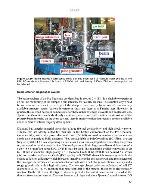
Figure 2.4.80: Beam induced fluorescence setup that has been used to measure beam profiles at the<br />
UNILAC accelerator. Uranium 28+ ions at 4.7 MeV/u with an intensity of 108 – 109 ions / macro-pulse can<br />
be detected.<br />
Beam catcher diagnostics system<br />
The beam catchers of the Pre-<strong>Separator</strong> are described in section 2.4.11.1. It is desirable to perform<br />
an on-line monitoring of the dumped beam intensity for security reasons. The simplest way would<br />
be to measure the transferred charge of the dumped ions directly by means of commercially<br />
available Ampere meters (current integrators), thus, use them as a Faraday cup. However, in<br />
practice this method becomes cumbersome for these rather extended movable and cooled devices.<br />
Apart from the optical methods already mentioned, where one could monitor the deposition of the<br />
primary beam intensity on the beam catcher, there is another option that recently became available<br />
and is subject to intense ongoing development.<br />
Diamond has superior material properties; a large thermal conductivity and high shock wave resistance<br />
that are ideally suited for their use in the hostile environment of the Pre-<strong>Separator</strong>.<br />
Commercially, artificially grown diamond films (CVD-D) are used as windows but became recently<br />
also available to build detectors. They are available as PolyCrystalline (PC) films, or even<br />
Single Crystal (SC) films, depending on how close the substrates properties, where they are grown<br />
on, are equal to the diamonds lattice. If nowadays, monolithic large area diamond detectors of a<br />
size > (8 x 8) mm 2 are needed, PC-CVD-D must be used. This material is available in wafers of up<br />
to 100 mm in diameter. High quality, i.e., Electronic Grade (EG) CVD-D can be used As Grown<br />
(AG) or polished to Detector Grade (DG) quality. AG CVD-D shows inhomogeneity in both, the<br />
charge collection efficiency which increases linearly along the crystals growth and the structure of<br />
the two opposite surfaces, i.e. a smooth substrate side with a bad charge collection efficiency and a<br />
rough growth side with a high efficiency. The average charge collection efficiency of AG PC<br />
diamond is 20 % - 40 %, meaning that more than half of the material thickness is electronically<br />
inactive. On the other hand this type of diamond provides the fastest detectors and, if needed, the<br />
thinnest free standing sensors. They can be ordered in layers of about 50�µm to 2 mm thickness. DG<br />
83