

AT91SAM ARM-based Flash MCU SAM3S8/SD8 Series - Atmel
AT91SAM ARM-based Flash MCU SAM3S8/SD8 Series - Atmel
AT91SAM ARM-based Flash MCU SAM3S8/SD8 Series - Atmel
- TAGS
- flash
- series
- atmel
- www.atmel.com

Create successful ePaper yourself
Turn your PDF publications into a flip-book with our unique Google optimized e-Paper software.
Features<br />
• Core<br />
– <strong>ARM</strong> ® Cortex ® -M3 revision 2.0 running at up to 64 MHz<br />
– Memory Protection Unit (MPU)<br />
–Thumb ® -2 instruction set<br />
Pin-to-pin compatible with <strong>AT91SAM</strong>7S legacy products (64-pin versions), SAM3S4/2/1<br />
products<br />
Memories<br />
– 512 Kbytes Single Plane (<strong>SAM3S8</strong>) embedded <strong>Flash</strong>, 128-bit wide access, memory<br />
accelerator<br />
– 512 Kbytes Dual Plane (SAM3<strong>SD8</strong>) embedded <strong>Flash</strong>, 128-bit wide access, memory<br />
accelerator<br />
– 64 Kbytes embedded SRAM<br />
– 16 Kbytes ROM with embedded boot loader routines (UART, USB) and IAP routines<br />
– 8-bit Static Memory Controller (SMC): SRAM, PSRAM, NOR and NAND <strong>Flash</strong><br />
support<br />
System<br />
– Embedded voltage regulator for single supply operation<br />
– Power-on-Reset (POR), Brown-out Detector (BOD) and Watchdog for safe operation<br />
– Quartz or ceramic resonator oscillators: 3 to 20 MHz main power with Failure<br />
Detection and optional low-power 32.768 kHz for RTC or device clock<br />
– RTC with Gregorian and Persian Calendar mode, waveform generation in lowpower<br />
modes<br />
– RTC clock calibration circuitry for 32.768 kHz crystal frequency compensation<br />
– High precision 8/12 MHz factory trimmed internal RC oscillator with 4 MHz default<br />
frequency for device startup. In-application trimming access for frequency<br />
adjustment<br />
– Slow Clock Internal RC oscillator as permanent low-power mode device clock<br />
– Two PLLs up to 130 MHz for device clock and for USB<br />
– Temperature Sensor<br />
– Up to 24 peripheral DMA (PDC) channels<br />
Low Power Modes<br />
– Sleep and Backup modes, down to < 2 µA in Backup mode<br />
– Ultra low-power RTC<br />
Peripherals<br />
– USB 2.0 Device: 12 Mbps, 2668 byte FIFO, up to 8 bidirectional Endpoints. On-Chip<br />
Transceiver<br />
– Up to 3 USARTs with ISO7816, IrDA ® , RS-485, SPI, Manchester and Modem Mode<br />
– Two 2-wire UARTs<br />
– Up to 2 Two Wire Interface (I2C compatible), 1 SPI, 1 Serial Synchronous Controller<br />
(I2S), 1 High Speed Multimedia Card Interface (SDIO/SD Card/MMC)<br />
– 6 Three-Channel 16-bit Timer/Counter with capture, waveform, compare and PWM<br />
mode. Quadrature Decoder Logic and 2-bit Gray Up/Down Counter for Stepper<br />
Motor<br />
– 4-channel 16-bit PWM with Complementary Output, Fault Input, 12-bit Dead Time<br />
Generator Counter for Motor Control<br />
– 32-bit Real-time Timer and RTC with calendar and alarm features<br />
– Up to 15-channel, 1Msps ADC with differential input mode and programmable gain<br />
stage and auto calibration<br />
– One 2-channel 12-bit 1Msps DAC<br />
– One Analog Comparator with flexible input selection, Selectable input hysteresis<br />
– 32-bit Cyclic Redundancy Check Calculation Unit (CRCCU)<br />
I/O<br />
– Up to 79 I/O lines with external interrupt capability (edge or level sensitivity),<br />
debouncing, glitch filtering and on-die <strong>Series</strong> Resistor Termination<br />
– Three 32-bit Parallel Input/Output Controllers, Peripheral DMA assisted Parallel<br />
Capture Mode<br />
Packages<br />
– 100-lead LQFP, 14 x 14 mm, pitch 0.5 mm/100-ball TFBGA, 9 x 9 mm, pitch 0.8 mm<br />
– 64-lead LQFP, 10 x 10 mm, pitch 0.5 mm/64-pad QFN 9x9 mm, pitch 0.5 mm<br />
<strong>AT91SAM</strong><br />
<strong>ARM</strong>-<strong>based</strong><br />
<strong>Flash</strong> <strong>MCU</strong><br />
<strong>SAM3S8</strong>/<strong>SD8</strong><br />
<strong>Series</strong><br />
11090A–AT<strong>ARM</strong>–10-Feb-12
1. Description<br />
2<br />
<strong>SAM3S8</strong>/<strong>SD8</strong><br />
The <strong>Atmel</strong> <strong>SAM3S8</strong>/<strong>SD8</strong> series is a member of a family of <strong>Flash</strong> microcontrollers <strong>based</strong> on the<br />
high performance 32-bit <strong>ARM</strong> Cortex-M3 RISC processor. It operates at a maximum speed of<br />
64 MHz and features up to 512 Kbytes of <strong>Flash</strong> (dual plane on SAM3<strong>SD8</strong>) and up to 64 Kbytes<br />
of SRAM. The peripheral set includes a Full Speed USB Device port with embedded transceiver,<br />
a High Speed MCI for SDIO/SD/MMC, an External Bus Interface featuring a Static Memory Controller<br />
providing connection to SRAM, PSRAM, NOR <strong>Flash</strong>, LCD Module and NAND <strong>Flash</strong>, 2(3)x<br />
USARTs, (3 on SAM3<strong>SD8</strong>C) 2x UARTs, 2x TWIs, 3x SPI, an I2S, as well as 1 PWM timer, 6x<br />
general-purpose 16-bit timers (with stepper motor and quadrature decoder logic support), an<br />
RTC, a 12-bit ADC, a 12-bit DAC and an analog comparator.<br />
The <strong>SAM3S8</strong>/<strong>SD8</strong> series is ready for capacitive touch thanks to the QTouch ® library, offering an<br />
easy way to implement buttons, wheels and sliders.<br />
The <strong>SAM3S8</strong>/<strong>SD8</strong> device is a medium range general purpose microcontroller with the best ratio<br />
in terms of reduced power consumption, processing power and peripheral set. This enables the<br />
<strong>SAM3S8</strong>/<strong>SD8</strong> to sustain a wide range of applications including consumer, industrial control, and<br />
PC peripherals.<br />
It operates from 1.62V to 3.6V and is available in 64- and 100-pin QFP, 64-pin QFN, and 100-pin<br />
BGA packages.<br />
The <strong>SAM3S8</strong>/<strong>SD8</strong> series is the ideal migration path from the SAM7S series for applications that<br />
require more performance. The <strong>SAM3S8</strong>/<strong>SD8</strong> series is pin-to-pin compatible with the<br />
SAM7Sseries.<br />
11090A–AT<strong>ARM</strong>–10-Feb-12
11090A–AT<strong>ARM</strong>–10-Feb-12<br />
<strong>SAM3S8</strong>/<strong>SD8</strong><br />
1.1 Configuration Summary<br />
The <strong>SAM3S8</strong>/<strong>SD8</strong> series devices differ in memory size, package and features. Table 1-1 summarizes<br />
the configurations of the device family.<br />
Table 1-1. Configuration Summary<br />
Feature <strong>SAM3S8</strong>B <strong>SAM3S8</strong>C SAM3<strong>SD8</strong>B SAM3<strong>SD8</strong>C<br />
<strong>Flash</strong> 512 Kbytes 512 Kbytes 512 Kbytes 512 Kbytes<br />
SRAM 64 Kbytes 64 Kbytes 64 Kbytes 64 Kbytes<br />
Package<br />
LQFP64<br />
QFN64<br />
LQFP100<br />
BGA100<br />
Notes: 1. Full Modem support on USART1.<br />
2. One channel is reserved for internal temperature sensor.<br />
LQFP64<br />
QFN64<br />
LQFP100<br />
BGA100<br />
Number of PIOs 47 79 47 79<br />
12-bit ADC 11 channels (2)<br />
16 channels (2)<br />
11 channels (2)<br />
16 channels (2)<br />
12-bit DAC 2 channels 2 channels 2 channels 2 channels<br />
Timer Counter<br />
Channels<br />
6 6 6 6<br />
PDC Channels 22 22 24 24<br />
USART/UART 2/2 (1)<br />
2/2 (1)<br />
2/2 (1)<br />
3/2 (1)<br />
HSMCI 1 port/4 bits 1 port/4 bits 1 port/4 bits 1 port/4 bits<br />
External Bus<br />
Interface<br />
-<br />
8-bit data,<br />
4 chip selects,<br />
24-bit address<br />
-<br />
8-bit data,<br />
4 chip selects,<br />
24-bit address<br />
3
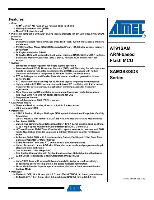
2. Block Diagram<br />
Figure 2-1. <strong>SAM3S8</strong>/<strong>SD8</strong> 100-pin version Block Diagram<br />
4<br />
TST<br />
PCK0-PCK2<br />
XIN<br />
XOUT<br />
WKUPx<br />
XIN32<br />
XOUT32<br />
ERASE<br />
VDDIO<br />
VDDCORE<br />
VDDPLL<br />
RTCOUT0<br />
RTCOUT1<br />
NRST<br />
TWCK0<br />
TWD0<br />
TWCK1<br />
TWD1<br />
URXD0<br />
UTXD0<br />
URXD1<br />
UTXD1<br />
RXD0<br />
TXD0<br />
SCK0<br />
RTS0<br />
CTS0<br />
RXD1<br />
TXD1<br />
SCK1<br />
RTS1<br />
CTS1<br />
DSR1<br />
DTR1<br />
RI1<br />
DCD1<br />
RXD2<br />
TXD2<br />
SCK2<br />
RTS2<br />
CTS2<br />
TCLK[0:2]<br />
TIOA[0:2]<br />
TIOB[0:2]<br />
TCLK[3:5]<br />
TIOA[3:5]<br />
TIOB[3:5]<br />
PWMH[0:3]<br />
PWML[0:3]<br />
PWMFI0<br />
ADTRG<br />
AD[0..14]<br />
ADVREF<br />
DAC0<br />
DAC1<br />
DATRG<br />
System Controller<br />
PLLA<br />
PLLB<br />
RC Osc<br />
12/8/4 MHz<br />
WDT<br />
3-20 MHz<br />
Osc<br />
SUPC<br />
Osc 32 kHz<br />
RC 32 kHz<br />
8 GPBREG<br />
RTT<br />
POR<br />
RTC<br />
RSTC<br />
SM<br />
<strong>SAM3S8</strong>/<strong>SD8</strong><br />
PMC<br />
PIOA / PIOB / PIOC<br />
TWI0<br />
TWI1<br />
UART0<br />
UART1<br />
USART0<br />
USART1<br />
PDC<br />
PDC<br />
PDC<br />
PDC<br />
PDC<br />
PDC<br />
USART2<br />
(SAM3<strong>SD8</strong> Only)<br />
Timer Counter B<br />
TC[0..2]<br />
Timer Counter B<br />
TC[3..5]<br />
PWM<br />
12-bit ADC<br />
12-bit DAC<br />
PDC<br />
PDC<br />
Temp. Sensor<br />
PDC<br />
PDC<br />
MPU<br />
TDI<br />
TDO<br />
TMS/SWDIO<br />
TCK/SWCLK<br />
JTAG & Serial Wire<br />
In-Circuit Emulator<br />
Cortex M-3 Processor<br />
Fmax 64 MHz<br />
I/D S<br />
Peripheral<br />
Bridge<br />
JTAGSEL<br />
24-Bit<br />
SysTick Counter<br />
N<br />
V<br />
I<br />
C<br />
Voltage<br />
Regulator<br />
<strong>Flash</strong><br />
Unique<br />
Identifier<br />
512 KBytes FLASH<br />
3-layer AHB Bus Matrix Fmax 64 MHz<br />
2668<br />
Bytes<br />
FIFO<br />
PDC<br />
PDC<br />
PDC<br />
PDC<br />
VDDIN<br />
VDDOUT<br />
<strong>SAM3S8</strong> Single Bank<br />
SAM3<strong>SD8</strong> Dual Bank<br />
USB 2.0<br />
Full<br />
Speed<br />
External Bus<br />
Interface<br />
NAND <strong>Flash</strong><br />
Logic<br />
Static Memory<br />
Controller<br />
PIO<br />
SPI<br />
SSC<br />
High Speed MCI<br />
Analog<br />
Comparator<br />
CRC Unit<br />
SRAM<br />
64 KBytes<br />
Transceiver<br />
ROM<br />
16 KBytes<br />
ADC Ch.<br />
PIO<br />
DDP<br />
DDM<br />
D[7:0]<br />
A[0:23]<br />
A21/NANDALE<br />
A22/NANDCLE<br />
NCS0<br />
NCS1<br />
NCS2<br />
NCS3<br />
NRD<br />
NWE<br />
NANDOE<br />
NANDWE<br />
NWAIT<br />
PIODC[7:0]<br />
PIODCEN1<br />
PIODCEN2<br />
PIODCCLK<br />
NPCS0<br />
NPCS1<br />
NPCS2<br />
NPCS3<br />
MISO<br />
MOSI<br />
SPCK<br />
TF<br />
TK<br />
TD<br />
RD<br />
RK<br />
RF<br />
MCCK<br />
MCCDA<br />
MCDA[0..3]<br />
ADVREF<br />
11090A–AT<strong>ARM</strong>–10-Feb-12
Figure 2-2. <strong>SAM3S8</strong>/<strong>SD8</strong> 64-pin version Block Diagram<br />
TST<br />
PCK0-PCK2<br />
11090A–AT<strong>ARM</strong>–10-Feb-12<br />
XIN<br />
XOUT<br />
WKUPx<br />
XIN32<br />
XOUT32<br />
ERASE<br />
VDDIO<br />
VDDCORE<br />
VDDPLL<br />
RTCOUT0<br />
RTCOUT1<br />
NRST<br />
TWCK0<br />
TWD0<br />
TWCK1<br />
TWD1<br />
URXD0<br />
UTXD0<br />
URXD1<br />
UTXD1<br />
RXD0<br />
TXD0<br />
SCK0<br />
RTS0<br />
CTS0<br />
RXD1<br />
TXD1<br />
SCK1<br />
RTS1<br />
CTS1<br />
DSR1<br />
DTR1<br />
RI1<br />
DCD1<br />
TCLK[0:2]<br />
TIOA[0:2]<br />
TIOB[0:2]<br />
PWMH[0:3]<br />
PWML[0:3]<br />
PWMFI0<br />
ADTRG<br />
AD[0..14]<br />
ADVREF<br />
DAC0<br />
DAC1<br />
DATRG<br />
System Controller<br />
PLLA<br />
PLLB<br />
RC Osc<br />
12/8/4 MHz<br />
WDT<br />
PMC<br />
3-20 MHz<br />
Osc<br />
SUPC<br />
Osc 32 kHz<br />
RC 32 kHz<br />
8 GPBREG<br />
RTT<br />
POR<br />
RTC<br />
RSTC<br />
PIOA / PIOB<br />
PIO<br />
SM<br />
TWI0<br />
TWI1<br />
UART0<br />
UART1<br />
USART0<br />
USART1<br />
Timer Counter A<br />
TC[0..2]<br />
PWM<br />
12-bit ADC<br />
12-bit DAC<br />
PDC<br />
PDC<br />
PDC<br />
PDC<br />
PDC<br />
PDC<br />
PDC<br />
PDC<br />
PDC<br />
MPU<br />
Temp. Sensor<br />
TDI<br />
TDO<br />
TMS/SWDIO<br />
TCK/SWCLK<br />
JTAG & Serial Wire<br />
In-Circuit Emulator<br />
Cortex M-3 Processor<br />
Fmax 64 MHz<br />
I/D S<br />
Peripheral<br />
Bridge<br />
JTAGSEL<br />
24-Bit<br />
SysTick Counter<br />
N<br />
V<br />
I<br />
C<br />
Voltage<br />
Regulator<br />
<strong>Flash</strong><br />
Unique<br />
Identifier<br />
512 KBytes FLASH<br />
3-layer AHB Bus Matrix Fmax 64 MHz<br />
2668<br />
Bytes<br />
FIFO<br />
PDC<br />
PDC<br />
PDC<br />
PDC<br />
VDDIN<br />
VDDOUT<br />
<strong>SAM3S8</strong> Single Bank<br />
SAM3<strong>SD8</strong> Dual Bank<br />
USB 2.0<br />
Full<br />
Speed<br />
PIO<br />
SPI<br />
SSC<br />
High Speed MCI<br />
Analog<br />
Comparator<br />
CRC Unit<br />
SRAM<br />
64 KBytes<br />
Transceiver<br />
ROM<br />
16 KBytes<br />
ADC Ch.<br />
PIO<br />
<strong>SAM3S8</strong>/<strong>SD8</strong><br />
DDP<br />
DDM<br />
PIODC[7:0]<br />
PIODCEN1<br />
PIODCEN2<br />
PIODCCLK<br />
NPCS0<br />
NPCS1<br />
NPCS2<br />
NPCS3<br />
MISO<br />
MOSI<br />
SPCK<br />
TF<br />
TK<br />
TD<br />
RD<br />
RK<br />
RF<br />
MCCK<br />
MCCDA<br />
MCDA[0..3]<br />
ADVREF<br />
5
3. Signal Description<br />
Table 3-1. Signal Description List<br />
6<br />
<strong>SAM3S8</strong>/<strong>SD8</strong><br />
Table 3-1 gives details on signal names classified by peripheral.<br />
Signal Name Function Type<br />
VDDIO<br />
VDDIN<br />
Peripherals I/O Lines and USB transceiver<br />
Power Supply<br />
Voltage Regulator Input, ADC, DAC and<br />
Analog Comparator Power Supply<br />
Power Supplies<br />
Active<br />
Level<br />
Voltage<br />
reference Comments<br />
Power 1.62V to 3.6V<br />
Power 1.8V to 3.6V (4)<br />
VDDOUT Voltage Regulator Output Power 1.8V Output<br />
VDDPLL Oscillator and PLL Power Supply Power 1.62 V to 1.95V<br />
VDDCORE<br />
Power the core, the embedded memories<br />
and the peripherals<br />
Power<br />
GND Ground Ground<br />
Supply Controller<br />
WKUPx Wake Up input pins input VDDIO<br />
Clocks, Oscillators and PLLs<br />
XIN Main Oscillator Input Input<br />
XOUT Main Oscillator Output Output<br />
XIN32 Slow Clock Oscillator Input Input<br />
XOUT32 Slow Clock Oscillator Output Output<br />
PCK0 - PCK2 Programmable Clock Output Output<br />
Real Time Clock<br />
RTCOUT0 Programmable RTC waveform output Output<br />
RTCOUT1 Programmable RTC waveform output Output<br />
Serial Wire/JTAG Debug Port - SWJ-DP<br />
VDDIO<br />
VDDIO<br />
1.62V to 1.95V<br />
Reset State:<br />
- PIO Input<br />
- Internal Pull-up disabled<br />
- Schmitt Trigger enabled (1)<br />
Reset State:<br />
- PIO Input<br />
- Internal Pull-up disabled<br />
- Schmitt Trigger enabled (1)<br />
Reset State:<br />
- PIO Input<br />
- Internal Pull-up enabled<br />
- Schmitt Trigger enabled (1)<br />
Reset State:<br />
- PIO Input<br />
- Internal Pull-up disabled<br />
- Schmitt Trigger enabled (1)<br />
11090A–AT<strong>ARM</strong>–10-Feb-12
Table 3-1. Signal Description List (Continued)<br />
Signal Name Function Type<br />
TCK/SWCLK Test Clock/Serial Wire Clock Input<br />
TDI Test Data In Input<br />
TDO/TRACESWO<br />
Test Data Out / Trace Asynchronous Data<br />
Out<br />
Output<br />
TMS/SWDIO Test Mode Select /Serial Wire Input/Output Input / I/O<br />
11090A–AT<strong>ARM</strong>–10-Feb-12<br />
Active<br />
Level<br />
JTAGSEL JTAG Selection Input High<br />
Voltage<br />
reference Comments<br />
VDDIO<br />
<strong>SAM3S8</strong>/<strong>SD8</strong><br />
Reset State:<br />
- SWJ-DP Mode<br />
- Internal pull-up disabled (5)<br />
- Schmitt Trigger enabled (1)<br />
Permanent Internal<br />
pull-down<br />
7
Table 3-1. Signal Description List (Continued)<br />
8<br />
Signal Name Function Type<br />
ERASE<br />
<strong>Flash</strong> and NVM Configuration Bits Erase<br />
Command<br />
<strong>SAM3S8</strong>/<strong>SD8</strong><br />
<strong>Flash</strong> Memory<br />
Reset/Test<br />
Input High VDDIO<br />
NRST Synchronous Microcontroller Reset I/O Low<br />
TST Test Select Input<br />
Universal Asynchronous Receiver Transceiver - UARTx<br />
URXDx UART Receive Data Input<br />
UTXDx UART Transmit Data Output<br />
PIO Controller - PIOA - PIOB - PIOC<br />
PA0 - PA31 Parallel IO Controller A I/O<br />
PB0 - PB14 Parallel IO Controller B I/O<br />
PC0 - PC31 Parallel IO Controller C I/O<br />
PIO Controller - Parallel Capture Mode<br />
PIODC0-PIODC7 Parallel Capture Mode Data Input<br />
PIODCCLK Parallel Capture Mode Clock Input<br />
PIODCEN1-2 Parallel Capture Mode Enable Input<br />
External Bus Interface<br />
D0 - D7 Data Bus I/O<br />
A0 - A23 Address Bus Output<br />
NWAIT External Wait Signal Input Low<br />
Static Memory Controller - SMC<br />
NCS0 - NCS3 Chip Select Lines Output Low<br />
NRD Read Signal Output Low<br />
NWE Write Enable Output Low<br />
NAND <strong>Flash</strong> Logic<br />
NANDOE NAND <strong>Flash</strong> Output Enable Output Low<br />
NANDWE NAND <strong>Flash</strong> Write Enable Output Low<br />
High Speed Multimedia Card Interface - HSMCI<br />
MCCK Multimedia Card Clock I/O<br />
MCCDA Multimedia Card Slot A Command I/O<br />
MCDA0 - MCDA3 Multimedia Card Slot A Data I/O<br />
Active<br />
Level<br />
Voltage<br />
reference Comments<br />
VDDIO<br />
VDDIO<br />
VDDIO<br />
Reset State:<br />
- Erase Input<br />
- Internal pull-down enabled<br />
- Schmitt Trigger enabled (1)<br />
Permanent Internal<br />
pull-up<br />
Permanent Internal<br />
pull-down<br />
Reset State:<br />
- PIO or System IOs (2)<br />
- Internal pull-up enabled<br />
- Schmitt Trigger enabled (1)<br />
11090A–AT<strong>ARM</strong>–10-Feb-12
Table 3-1. Signal Description List (Continued)<br />
Signal Name Function Type<br />
11090A–AT<strong>ARM</strong>–10-Feb-12<br />
Universal Synchronous Asynchronous Receiver Transmitter USARTx<br />
SCKx USARTx Serial Clock I/O<br />
TXDx USARTx Transmit Data I/O<br />
RXDx USARTx Receive Data Input<br />
RTSx USARTx Request To Send Output<br />
CTSx USARTx Clear To Send Input<br />
DTR1 USART1 Data Terminal Ready I/O<br />
DSR1 USART1 Data Set Ready Input<br />
DCD1 USART1 Data Carrier Detect Output<br />
RI1 USART1 Ring Indicator Input<br />
Synchronous Serial Controller - SSC<br />
TD SSC Transmit Data Output<br />
RD SSC Receive Data Input<br />
TK SSC Transmit Clock I/O<br />
RK SSC Receive Clock I/O<br />
TF SSC Transmit Frame Sync I/O<br />
RF SSC Receive Frame Sync I/O<br />
Timer/Counter - TC<br />
TCLKx TC Channel x External Clock Input Input<br />
TIOAx TC Channel x I/O Line A I/O<br />
TIOBx TC Channel x I/O Line B I/O<br />
Pulse Width Modulation Controller- PWMC<br />
PWMHx PWM Waveform Output High for channel x Output<br />
PWMLx PWM Waveform Output Low for channel x Output<br />
PWMFI0 PWM Fault Input Input<br />
Serial Peripheral Interface - SPI<br />
MISO Master In Slave Out I/O<br />
MOSI Master Out Slave In I/O<br />
SPCK SPI Serial Clock I/O<br />
SPI_NPCS0 SPI Peripheral Chip Select 0 I/O Low<br />
SPI_NPCS1 -<br />
SPI_NPCS3<br />
Active<br />
Level<br />
SPI Peripheral Chip Select Output Low<br />
Voltage<br />
reference Comments<br />
<strong>SAM3S8</strong>/<strong>SD8</strong><br />
only output in<br />
complementary mode when<br />
dead time insertion is<br />
enabled.<br />
9
Table 3-1. Signal Description List (Continued)<br />
Signal Name Function Type<br />
Note: 1. Schmitt Triggers can be disabled through PIO registers.<br />
2. Some PIO lines are shared with System I/Os.<br />
3. Refer to USB Section of the product Electrical Characteristics for information on Pull-down value in USB Mode.<br />
4. See “Typical Powering Schematics” Section for restrictions on voltage range of Analog Cells.<br />
5. TDO pin is set in input mode when the Cortex-M3 Core is not in debug mode. Thus the internal pull-up corresponding to this<br />
PIO line must be enabled to avoid current consumption due to floating input.<br />
10<br />
<strong>SAM3S8</strong>/<strong>SD8</strong><br />
Two-Wire Interface- TWI<br />
TWDx TWIx Two-wire Serial Data I/O<br />
TWCKx TWIx Two-wire Serial Clock I/O<br />
ADVREF<br />
AD0 - AD14 Analog Inputs<br />
Analog<br />
ADC, DAC and Analog Comparator<br />
Analog<br />
Reference<br />
12-bit Analog-to-Digital Converter - ADC<br />
Analog,<br />
Digital<br />
ADTRG ADC Trigger Input VDDIO<br />
DAC0 - DAC1 Analog output<br />
12-bit Digital-to-Analog Converter - DAC<br />
Analog,<br />
Digital<br />
DACTRG DAC Trigger Input VDDIO<br />
Fast <strong>Flash</strong> Programming Interface - FFPI<br />
PGMEN0-PGMEN2 Programming Enabling Input VDDIO<br />
PGMM0-PGMM3 Programming Mode Input<br />
PGMD0-PGMD15 Programming Data I/O<br />
PGMRDY Programming Ready Output High<br />
PGMNVALID Data Direction Output Low<br />
PGMNOE Programming Read Input Low<br />
PGMCK Programming Clock Input<br />
PGMNCMD Programming Command Input Low<br />
DDM USB Full Speed Data -<br />
DDP USB Full Speed Data +<br />
USB Full Speed Device<br />
Analog,<br />
Digital<br />
Active<br />
Level<br />
Voltage<br />
reference Comments<br />
VDDIO<br />
VDDIO<br />
Reset State:<br />
- USB Mode<br />
- Internal Pull-down (3)<br />
11090A–AT<strong>ARM</strong>–10-Feb-12
4. Package and Pinout<br />
11090A–AT<strong>ARM</strong>–10-Feb-12<br />
<strong>SAM3S8</strong>/<strong>SD8</strong><br />
<strong>SAM3S8</strong>/<strong>SD8</strong> devices are pin-to-pin compatible with <strong>AT91SAM</strong>7S legacy products for 64-pin<br />
version. Furthermore, <strong>SAM3S8</strong>/<strong>SD8</strong> products have new functionalities referenced in italic in<br />
Table 4-1, Table 4-3.<br />
4.1 <strong>SAM3S8</strong>C/8DC Package and Pinout<br />
4.1.1 100-Lead LQFP Package Outline<br />
Figure 4-1. Orientation of the 100-lead LQFP Package<br />
4.1.2 100-ball TFBGA Package Outline<br />
The 100-Ball TFBGA package has a 0.8 mm ball pitch and respects Green Standards. Its<br />
dimensions are 9 x 9 x 1.1 mm. Figure 4-2 shows the orientation of the 100-ball TFBGA<br />
Package.<br />
Figure 4-2. Orientation of the 100-ball TFBGA Package<br />
76<br />
100<br />
BALL A1<br />
75<br />
51<br />
1 25<br />
10<br />
9<br />
8<br />
7<br />
6<br />
5<br />
4<br />
3<br />
2<br />
1<br />
TOP VIEW<br />
A B C D E F G H J K<br />
50<br />
26<br />
11
4.1.3 100-Lead LQFP Pinout<br />
Table 4-1. <strong>SAM3S8</strong>C/<strong>SD8</strong>C 100-lead LQFP pinout<br />
12<br />
1 ADVREF 26 GND 51 TDI/PB4 76<br />
<strong>SAM3S8</strong>/<strong>SD8</strong><br />
TDO/TRACESWO/<br />
PB5<br />
2 GND 27 VDDIO 52 PA6/PGMNOE 77 JTAGSEL<br />
3 PB0/AD4 28 PA16/PGMD4 53 PA5/PGMRDY 78 PC18<br />
4 PC29/AD13 29 PC7 54 PC28 79 TMS/SWDIO/PB6<br />
5 PB1/AD5 30 PA15/PGMD3 55 PA4/PGMNCMD 80 PC19<br />
6 PC30/AD14 31 PA14/PGMD2 56 VDDCORE 81 PA31<br />
7 PB2/AD6 32 PC6 57 PA27/PGMD15 82 PC20<br />
8 PC31 33 PA13/PGMD1 58 PC8 83 TCK/SWCLK/PB7<br />
9 PB3/AD7 34 PA24/PGMD12 59 PA28 84 PC21<br />
10 VDDIN 35 PC5 60 NRST 85 VDDCORE<br />
11 VDDOUT 36 VDDCORE 61 TST 86 PC22<br />
12 PA17/PGMD5/AD0 37 PC4 62 PC9 87 ERASE/PB12<br />
13 PC26 38 PA25/PGMD13 63 PA29 88 DDM/PB10<br />
14 PA18/PGMD6/AD1 39 PA26/PGMD14 64 PA30 89 DDP/PB11<br />
15 PA21/PGMD9/AD8 40 PC3 65 PC10 90 PC23<br />
16 VDDCORE 41 PA12/PGMD0 66 PA3 91 VDDIO<br />
17 PC27 42 PA11/PGMM3 67 PA2/PGMEN2 92 PC24<br />
18 PA19/PGMD7/AD2 43 PC2 68 PC11 93 PB13/DAC0<br />
19 PC15/AD11 44 PA10/PGMM2 69 VDDIO 94 PC25<br />
20<br />
PA22/PGMD10/AD<br />
9<br />
45 GND 70 GND 95 GND<br />
21 PC13/AD10 46 PA9/PGMM1 71 PC14 96 PB8/XOUT<br />
22 PA23/PGMD11 47 PC1 72 PA1/PGMEN1 97 PB9/PGMCK/XIN<br />
23 PC12/AD12 48<br />
PA8/XOUT32/<br />
PGMM0<br />
73 PC16 98 VDDIO<br />
24 PA20/PGMD8/AD3 49<br />
PA7/XIN32/<br />
PGMNVALID<br />
74 PA0/PGMEN0 99 PB14/DAC1<br />
25 PC0 50 VDDIO 75 PC17 100 VDDPLL<br />
11090A–AT<strong>ARM</strong>–10-Feb-12
4.1.4 100-Ball TFBGA Pinout<br />
Table 4-2. <strong>SAM3S8</strong>C/<strong>SD8</strong>C 100-ball TFBGA pinout<br />
11090A–AT<strong>ARM</strong>–10-Feb-12<br />
<strong>SAM3S8</strong>/<strong>SD8</strong><br />
A1 PB1/AD5 C6 TCK/SWCLK/PB7 F1 PA18/PGMD6/AD1 H6 PC4<br />
A2 PC29 C7 PC16 F2 PC26 H7 PA11/PGMM3<br />
A3 VDDIO C8 PA1/PGMEN1 F3 VDDOUT H8 PC1<br />
A4 PB9/PGMCK/XIN C9 PC17 F4 GND H9 PA6/PGMNOE<br />
A5 PB8/XOUT C10 PA0/PGMEN0 F5 VDDIO H10 TDI/PB4<br />
A6 PB13/DAC0 D1 PB3/AD7 F6 PA27/PGMD15 J1 PC15/AD11<br />
A7 DDP/PB11 D2 PB0/AD4 F7 PC8 J2 PC0<br />
A8 DDM/PB10 D3 PC24 F8 PA28 J3 PA16/PGMD4<br />
A9 TMS/SWDIO/PB6 D4 PC22 F9 TST J4 PC6<br />
A10 JTAGSEL D5 GND F10 PC9 J5 PA24/PGMD12<br />
B1 PC30 D6 GND G1 PA21/PGMD9/AD8 J6 PA25/PGMD13<br />
B2 ADVREF D7 VDDCORE G2 PC27 J7 PA10/PGMM2<br />
B3 GNDANA D8 PA2/PGMEN2 G3 PA15/PGMD3 J8 GND<br />
B4 PB14/DAC1 D9 PC11 G4 VDDCORE J9 VDDCORE<br />
B5 PC21 D10 PC14 G5 VDDCORE J10 VDDIO<br />
B6 PC20 E1<br />
PA17/PGMD5/AD<br />
0<br />
G6 PA26/PGMD14 K1<br />
PA22/PGMD10/AD<br />
9<br />
B7 PA31 E2 PC31 G7 PA12/PGMD0 K2 PC13/AD10<br />
B8 PC19 E3 VDDIN G8 PC28 K3 PC12/AD12<br />
B9 PC18 E4 GND G9 PA4/PGMNCMD K4 PA20/PGMD8/AD3<br />
B10<br />
TDO/TRACESWO/<br />
PB5<br />
E5 GND G10 PA5/PGMRDY K5 PC5<br />
C1 PB2/AD6 E6 NRST H1 PA19/PGMD7/AD2 K6 PC3<br />
C2 VDDPLL E7 PA29/AD13 H2 PA23/PGMD11 K7 PC2<br />
C3 PC25 E8 PA30/AD14 H3 PC7 K8 PA9/PGMM1<br />
C4 PC23 E9 PC10 H4 PA14/PGMD2 K9<br />
C5 ERASE/PB12 E10 PA3 H5 PA13/PGMD1 K10<br />
PA8/XOUT32/PGM<br />
M0<br />
PA7/XIN32/<br />
PGMNVALID<br />
13
4.2 <strong>SAM3S8</strong>B/D8B Package and Pinout<br />
4.2.1 64-Lead LQFP Package Outline<br />
4.2.2 64-lead QFN Package Outline<br />
14<br />
<strong>SAM3S8</strong>/<strong>SD8</strong><br />
Figure 4-3. Orientation of the 64-lead LQFP Package<br />
Figure 4-4. Orientation of the 64-lead QFN Package<br />
1<br />
49<br />
64<br />
64<br />
48<br />
1<br />
33<br />
16<br />
49<br />
32<br />
17<br />
48<br />
16<br />
33<br />
17<br />
TOP VIEW<br />
32<br />
11090A–AT<strong>ARM</strong>–10-Feb-12
4.2.3 64-Lead LQFP and QFN Pinout<br />
Table 4-3. 64-pin <strong>SAM3S8</strong>B/D8B pinout<br />
1 ADVREF 17 GND 33 TDI/PB4 49<br />
Note: The bottom pad of the QFN package must be connected to ground.<br />
11090A–AT<strong>ARM</strong>–10-Feb-12<br />
<strong>SAM3S8</strong>/<strong>SD8</strong><br />
TDO/TRACESWO/<br />
PB5<br />
2 GND 18 VDDIO 34 PA6/PGMNOE 50 JTAGSEL<br />
3 PB0/AD4 19 PA16/PGMD4 35 PA5/PGMRDY 51 TMS/SWDIO/PB6<br />
4 PB1/AD5 20 PA15/PGMD3 36 PA4/PGMNCMD 52 PA31<br />
5 PB2/AD6 21 PA14/PGMD2 37 PA27/PGMD15 53 TCK/SWCLK/PB7<br />
6 PB3/AD7 22 PA13/PGMD1 38 PA28 54 VDDCORE<br />
7 VDDIN 23 PA24/PGMD12 39 NRST 55 ERASE/PB12<br />
8 VDDOUT 24 VDDCORE 40 TST 56 DDM/PB10<br />
9<br />
10<br />
PA17/PGMD5/<br />
AD0<br />
PA18/PGMD6/<br />
AD1<br />
25 PA25/PGMD13 41 PA29 57 DDP/PB11<br />
26 PA26/PGMD14 42 PA30 58 VDDIO<br />
11<br />
PA21/PGMD9/<br />
AD8<br />
27 PA12/PGMD0 43 PA3 59 PB13/DAC0<br />
12 VDDCORE 28 PA11/PGMM3 44 PA2/PGMEN2 60 GND<br />
13<br />
14<br />
PA19/PGMD7/<br />
AD2<br />
PA22/PGMD10/<br />
AD9<br />
15 PA23/PGMD11 31<br />
16<br />
PA20/PGMD8/<br />
AD3<br />
29 PA10/PGMM2 45 VDDIO 61 XOUT/PB8<br />
30 PA9/PGMM1 46 GND 62 XIN/PGMCK/PB9<br />
32<br />
PA8/XOUT32/<br />
PGMM0<br />
PA7/XIN32/<br />
PGMNVALID<br />
47 PA1/PGMEN1 63 PB14/DAC1<br />
48 PA0/PGMEN0 64 VDDPLL<br />
15
5. Power Considerations<br />
5.1 Power Supplies<br />
The <strong>SAM3S8</strong>/<strong>SD8</strong> has several types of power supply pins:<br />
16<br />
<strong>SAM3S8</strong>/<strong>SD8</strong><br />
VDDCORE pins: Power the core, the embedded memories and the peripherals. Voltage<br />
ranges from 1.62V to 1.95V.<br />
VDDIO pins: Power the Peripherals I/O lines (Input/Output Buffers), USB transceiver, Backup<br />
part, 32 kHz crystal oscillator and oscillator pads. Voltage ranges from 1.62V to 3.6V.<br />
VDDIN pin: Voltage Regulator Input, ADC, DAC and Analog Comparator Power Supply.<br />
Voltage ranges from 1.8V to 3.6V.<br />
VDDPLL pin: Powers the PLLA, PLLB, the Fast RC and the 3 to 20 MHz oscillator. Voltage<br />
ranges from 1.62V to 1.95V.<br />
5.2 Voltage Regulator<br />
The <strong>SAM3S8</strong>/<strong>SD8</strong> embeds a voltage regulator that is managed by the Supply Controller.<br />
This internal regulator is designed to supply the internal core of <strong>SAM3S8</strong>/<strong>SD8</strong>. It features two<br />
operating modes:<br />
In Normal mode, the voltage regulator consumes less than 700 µA static current and draws<br />
80 mA of output current. Internal adaptive biasing adjusts the regulator quiescent current<br />
depending on the required load current. In Wait Mode quiescent current is only 7 µA.<br />
In Backup mode, the voltage regulator consumes less than 1 µA while its output (VDDOUT)<br />
is driven internally to GND. The default output voltage is 1.80V and the start-up time to reach<br />
Normal mode is less than 100 µs.<br />
For adequate input and output power supply decoupling/bypassing, refer to the “Voltage Regulator”<br />
section in the “Electrical Characteristics” section of the datasheet.<br />
5.3 Typical Powering Schematics<br />
The <strong>SAM3S8</strong>/<strong>SD8</strong> supports a 1.62V-3.6V single supply mode. The internal regulator input is<br />
connected to the source and its output feeds VDDCORE. Figure 5-1 below shows the power<br />
schematics.<br />
As VDDIN powers the voltage regulator, the ADC, DAC and the analog comparator, when the<br />
user does not want to use the embedded voltage regulator, it can be disabled by software via<br />
the SUPC (note that this is different from Backup mode).<br />
11090A–AT<strong>ARM</strong>–10-Feb-12
11090A–AT<strong>ARM</strong>–10-Feb-12<br />
Figure 5-1. Single Supply<br />
Note: Restrictions<br />
For USB, VDDIO needs to be greater than 3.0V.<br />
For ADC, VDDIN needs to be greater than 2.0V.<br />
For DAC, VDDIN needs to be greater than 2.4V.<br />
Figure 5-2. Core Externally Supplied<br />
VDDIO<br />
USB<br />
Transceivers.<br />
Main Supply<br />
(1.8V-3.6V) ADC, DAC<br />
Analog Comp.<br />
VDDIN<br />
Main Supply<br />
(1.62V-3.6V)<br />
Can be the<br />
same supply<br />
ADC, DAC, Analog<br />
Comparator Supply<br />
(2.0V-3.6V)<br />
VDDCORE Supply<br />
(1.62V-1.95V)<br />
VDDOUT<br />
VDDCORE<br />
VDDPLL<br />
VDDIO<br />
VDDIN<br />
Note: Restrictions<br />
For USB, VDDIO needs to be greater than 3.0V.<br />
For ADC, VDDIN needs to be greater than 2.0V.<br />
For DAC, VDDIN needs to be greater than 2.4V.<br />
VDDOUT<br />
VDDCORE<br />
VDDPLL<br />
Voltage<br />
Regulator<br />
USB<br />
Transceivers.<br />
ADC, DAC<br />
Analog Comp.<br />
Voltage<br />
Regulator<br />
<strong>SAM3S8</strong>/<strong>SD8</strong><br />
Figure 5-3 below provides an example of the powering scheme when using a backup battery.<br />
Since the PIO state is preserved when in backup mode, any free PIO line can be used to switch<br />
off the external regulator by driving the PIO line at low level (PIO is input, pull-up enabled after<br />
backup reset). External wake-up of the system can be from a push button or any signal. See<br />
Section 5.6 “Wake-up Sources” for further details.<br />
17
5.4 Active Mode<br />
18<br />
<strong>SAM3S8</strong>/<strong>SD8</strong><br />
Figure 5-3. Backup Battery<br />
Active mode is the normal running mode with the core clock running from the fast RC oscillator,<br />
the main crystal oscillator or the PLLA. The power management controller can be used to adapt<br />
the frequency and to disable the peripheral clocks.<br />
5.5 Low-power Modes<br />
The various low-power modes of the <strong>SAM3S8</strong>/<strong>SD8</strong> are described below:<br />
5.5.1 Backup Mode<br />
Main Supply<br />
Backup<br />
Battery +<br />
-<br />
IN OUT<br />
3.3V<br />
LDO<br />
ON/OFF<br />
ADC, DAC, Analog<br />
Comparator Supply<br />
(2.0V-3.6V)<br />
VDDIO<br />
VDDIN<br />
VDDOUT<br />
VDDCORE<br />
VDDPLL<br />
External wakeup signal<br />
Note: The two diodes provide a “switchover circuit” (for illustration purpose)<br />
between the backup battery and the main supply when the system is put in<br />
backup mode.<br />
The purpose of backup mode is to achieve the lowest power consumption possible in a system<br />
which is performing periodic wake-ups to perform tasks but not requiring fast startup time<br />
(
5.5.2 Wait Mode<br />
5.5.3 Sleep Mode<br />
11090A–AT<strong>ARM</strong>–10-Feb-12<br />
Supply Monitor alarm<br />
RTC alarm<br />
RTT alarm<br />
<strong>SAM3S8</strong>/<strong>SD8</strong><br />
The purpose of the wait mode is to achieve very low power consumption while maintaining the<br />
whole device in a powered state for a startup time of less than 10 µs. Current Consumption in<br />
Wait mode is typically 20 µA (total current consumption) if the internal voltage regulator is used<br />
or 12 µA if an external regulator is used.<br />
In this mode, the clocks of the core, peripherals and memories are stopped. However, the core,<br />
peripherals and memories power supplies are still powered. From this mode, a fast start up is<br />
available.<br />
This mode is entered via Wait for Event (WFE) instructions with LPM = 1 (Low Power Mode bit in<br />
PMC_FSMR). The Cortex-M3 is able to handle external events or internal events in order to<br />
wake-up the core (WFE). This is done by configuring the external lines WUP0-15 as fast startup<br />
wake-up pins (refer to Section 5.7 “Fast Startup”). RTC or RTT Alarm and USB wake-up events<br />
can be used to wake up the CPU (exit from WFE).<br />
Entering Wait Mode:<br />
Select the 4/8/12 MHz fast RC oscillator as Main Clock<br />
Set the LPM bit in the PMC Fast Startup Mode Register (PMC_FSMR)<br />
Execute the Wait-For-Event (WFE) instruction of the processor<br />
Note: Internal Main clock resynchronization cycles are necessary between the writing of MOSCRCEN<br />
bit and the effective entry in Wait mode. Depending on the user application, waiting for<br />
MOSCRCEN bit to be cleared is recommended to ensure that the core will not execute undesired<br />
instructions.<br />
The purpose of sleep mode is to optimize power consumption of the device versus response<br />
time. In this mode, only the core clock is stopped. The peripheral clocks can be enabled. The<br />
current consumption in this mode is application dependent.<br />
This mode is entered via Wait for Interrupt (WFI) or Wait for Event (WFE) instructions with<br />
LPM = 0 in PMC_FSMR.<br />
The processor can be awakened from an interrupt if WFI instruction of the Cortex M3 is used, or<br />
from an event if the WFE instruction is used to enter this mode.<br />
19
5.5.4 Low Power Mode Summary Table<br />
The modes detailed above are the main low-power modes. Each part can be set to on or off separately<br />
and wake up sources can be individually configured. Table 5-1 below shows a summary<br />
of the configurations of the low-power modes.<br />
Table 5-1. Low-power Mode Configuration Summary<br />
Mode<br />
Backup<br />
Mode<br />
Wait<br />
Mode<br />
Sleep<br />
Mode<br />
Notes: 1. When considering wake-up time, the time required to start the PLL is not taken into account. Once started, the device works<br />
with the 4/8/12 MHz fast RC oscillator. The user has to add the PLL start-up time if it is needed in the system. The wake-up<br />
time is defined as the time taken for wake up until the first instruction is fetched.<br />
2. The external loads on PIOs are not taken into account in the calculation.<br />
3. Supply Monitor current consumption is not included.<br />
4. Total Current consumption.<br />
5. Total current consumption (without using internal voltage regulator) / Total current consumption (using internal voltage<br />
regulator).<br />
6. Depends on MCK frequency.<br />
7. In this mode the core is supplied and not clocked but some peripherals can be clocked.<br />
20<br />
SUPC,<br />
32 kHz<br />
Oscillator,<br />
RTC, RTT<br />
Backup<br />
Registers,<br />
POR<br />
(Backup<br />
Region) Regulator<br />
ON OFF<br />
ON ON<br />
ON ON<br />
<strong>SAM3S8</strong>/<strong>SD8</strong><br />
Core<br />
Memory<br />
Peripherals Mode Entry<br />
OFF<br />
(Not powered)<br />
Powered<br />
(Not clocked)<br />
Powered (7)<br />
(Not clocked)<br />
WFE<br />
+SLEEPDEEP<br />
bit = 1<br />
WFE<br />
+SLEEPDEEP<br />
bit = 0<br />
+LPM bit = 1<br />
WFE or WFI<br />
+SLEEPDEEP<br />
bit = 0<br />
+LPM bit = 0<br />
Potential Wake Up<br />
Sources<br />
WUP0-15 pins<br />
SM alarm<br />
RTC alarm<br />
RTT alarm<br />
Any Event from: Fast<br />
startup through<br />
WUP0-15 pins<br />
RTC alarm<br />
RTT alarm<br />
USB wake-up<br />
Core at<br />
Wake Up<br />
Reset<br />
Clocked<br />
back<br />
Entry mode =WFI<br />
Interrupt Only; Entry<br />
mode =WFE Any<br />
Enabled Interrupt<br />
and/or Any Event<br />
Clocked<br />
from: Fast start-up<br />
back<br />
through WUP0-15<br />
pins<br />
RTC alarm<br />
RTT alarm<br />
USB wake-up<br />
PIO State<br />
while in Low<br />
Power Mode<br />
Previous<br />
state saved<br />
PIO State<br />
at Wake Up<br />
PIOA &<br />
PIOB &<br />
PIOC<br />
Inputs with<br />
pull ups<br />
Consumption<br />
(2) (3)<br />
Wake-up<br />
Time (1)<br />
< 2 µA typ (4) < 0.1 ms<br />
Previous<br />
state saved Unchanged 12 µA/20 µA (5) < 10 µs<br />
Previous<br />
state saved<br />
Unchanged (6) (6)<br />
11090A–AT<strong>ARM</strong>–10-Feb-12
11090A–AT<strong>ARM</strong>–10-Feb-12<br />
<strong>SAM3S8</strong>/<strong>SD8</strong><br />
5.6 Wake-up Sources<br />
The wake-up events allow the device to exit the backup mode. When a wake-up event is<br />
detected, the Supply Controller performs a sequence which automatically reenables the core<br />
power supply and the SRAM power supply, if they are not already enabled.<br />
Figure 5-4. Wake-up Source<br />
WKUP0<br />
WKUP1<br />
WKUP15<br />
sm_out<br />
rtc_alarm<br />
rtt_alarm<br />
WKUPT0<br />
Falling/Rising<br />
Edge<br />
Detector<br />
WKUPT1<br />
Falling/Rising<br />
Edge<br />
Detector<br />
WKUPT15<br />
Falling/Rising<br />
Edge<br />
Detector<br />
SMEN<br />
RTCEN<br />
RTTEN<br />
WKUPEN0<br />
WKUPEN1<br />
WKUPEN15<br />
WKUPIS0<br />
WKUPIS1<br />
WKUPIS15<br />
SLCK<br />
WKUPDBC<br />
Debouncer<br />
WKUPS<br />
Core<br />
Supply<br />
Restart<br />
21
5.7 Fast Startup<br />
22<br />
<strong>SAM3S8</strong>/<strong>SD8</strong><br />
The <strong>SAM3S8</strong>/<strong>SD8</strong> allows the processor to restart in a few microseconds while the processor is<br />
in wait mode or in sleep mode. A fast start up can occur upon detection of a low level on one of<br />
the 19 wake-up inputs (WKUP0 to 15 + SM + RTC + RTT).<br />
The fast restart circuitry, as shown in Figure 5-5, is fully asynchronous and provides a fast startup<br />
signal to the Power Management Controller. As soon as the fast start-up signal is asserted,<br />
the PMC automatically restarts the embedded 4 MHz Fast RC oscillator, switches the master<br />
clock on this 4MHz clock and reenables the processor clock.<br />
Figure 5-5. Fast Start-Up Sources<br />
WKUP0<br />
WKUP1<br />
WKUP15<br />
usb_wakeup<br />
rtc_alarm<br />
rtt_alarm<br />
Falling/Rising<br />
Edge<br />
Detector<br />
Falling/Rising<br />
Edge<br />
Detector<br />
Falling/Rising<br />
Edge<br />
Detector<br />
USBEN<br />
RTCEN<br />
RTTEN<br />
FSTT0<br />
FSTT1<br />
FSTT15<br />
fast_restart<br />
11090A–AT<strong>ARM</strong>–10-Feb-12
6. Input/Output Lines<br />
11090A–AT<strong>ARM</strong>–10-Feb-12<br />
<strong>SAM3S8</strong>/<strong>SD8</strong><br />
The <strong>SAM3S8</strong>/<strong>SD8</strong> has several kinds of input/output (I/O) lines such as general purpose I/Os<br />
(GPIO) and system I/Os. GPIOs can have alternate functionality due to multiplexing capabilities<br />
of the PIO controllers. The same PIO line can be used whether in I/O mode or by the multiplexed<br />
peripheral. System I/Os include pins such as test pins, oscillators, erase or analog inputs.<br />
6.1 General Purpose I/O Lines<br />
GPIO Lines are managed by PIO Controllers. All I/Os have several input or output modes such<br />
as pull-up or pull-down, input Schmitt triggers, multi-drive (open-drain), glitch filters, debouncing<br />
or input change interrupt. Programming of these modes is performed independently for each I/O<br />
line through the PIO controller user interface. For more details, refer to the product “PIO Controller”<br />
section.<br />
The input/output buffers of the PIO lines are supplied through VDDIO power supply rail.<br />
The <strong>SAM3S8</strong>/<strong>SD8</strong> embeds high speed pads able to handle up to 32 MHz for HSMCI (MCK/2),<br />
45 MHz for SPI clock lines and 35 MHz on other lines. See AC Characteristics Section of the<br />
datasheet for more details. Typical pull-up and pull-down value is 100 kΩ for all I/Os.<br />
Each I/O line also embeds an ODT (On-Die Termination), (see Figure 6-1 below). It consists of<br />
an internal series resistor termination scheme for impedance matching between the driver output<br />
(<strong>SAM3S8</strong>/<strong>SD8</strong>) and the PCB trace impedance preventing signal reflection. The series<br />
resistor helps to reduce IOs switching current (di/dt) thereby reducing in turn, EMI. It also<br />
decreases overshoot and undershoot (ringing) due to inductance of interconnect between<br />
devices or between boards. In conclusion ODT helps diminish signal integrity issues.<br />
Figure 6-1. On-Die Termination<br />
SAM3 Driver with<br />
Zout ~ 10 Ohms<br />
ODT<br />
36 Ohms Typ.<br />
PCB Trace<br />
Z0 ~ 50 Ohms<br />
Receiver<br />
6.2 System I/O Lines<br />
System I/O lines are pins used by oscillators, test mode, reset and JTAG to name but a few.<br />
Described below in Table 6-1are the <strong>SAM3S8</strong>/<strong>SD8</strong> system I/O lines shared with PIO lines.<br />
Rodt<br />
Z0 ~ Zout + Rodt<br />
These pins are software configurable as general purpose I/O or system pins. At startup the<br />
default function of these pins is always used.<br />
23
Table 6-1. System I/O Configuration Pin List.<br />
Notes: 1. If PB12 is used as PIO input in user applications, a low level must be ensured at startup to prevent <strong>Flash</strong> erase before the<br />
user application sets PB12 into PIO mode,<br />
2. In the product Datasheet Refer to: “Slow Clock Generator” of the “Supply Controller” section.<br />
3. In the product Datasheet Refer to: “3 to 20 MHZ Crystal Oscillator” information in the “PMC” section.<br />
24<br />
SYSTEM_IO<br />
bit number<br />
6.2.1 Serial Wire JTAG Debug Port (SWJ-DP) Pins<br />
The SWJ-DP pins are TCK/SWCLK, TMS/SWDIO, TDO/SWO, TDI and commonly provided on<br />
a standard 20-pin JTAG connector defined by <strong>ARM</strong>. For more details about voltage reference<br />
and reset state, refer to Table 3-1 on page 6.<br />
<strong>SAM3S8</strong>/<strong>SD8</strong><br />
Default function<br />
after reset Other function<br />
12 ERASE PB12 Low Level at startup (1)<br />
10 DDM PB10 -<br />
11 DDP PB11 -<br />
7 TCK/SWCLK PB7 -<br />
6 TMS/SWDIO PB6 -<br />
5 TDO/TRACESWO PB5 -<br />
4 TDI PB4 -<br />
- PA7 XIN32 -<br />
- PA8 XOUT32 -<br />
- PB9 XIN -<br />
- PB8 XOUT -<br />
Constraints for<br />
normal start Configuration<br />
In Matrix User Interface Registers<br />
(Refer to the System I/O<br />
Configuration Register in the “Bus<br />
Matrix” section of the datasheet.)<br />
See footnote (2) below<br />
See footnote (3) below<br />
At startup, SWJ-DP pins are configured in SWJ-DP mode to allow connection with debugging<br />
probe. Please refer to the “Debug and Test” Section of the product datasheet.<br />
SWJ-DP pins can be used as standard I/Os to provide users more general input/output pins<br />
when the debug port is not needed in the end application. Mode selection between SWJ-DP<br />
mode (System IO mode) and general IO mode is performed through the AHB Matrix Special<br />
Function Registers (MATRIX_SFR). Configuration of the pad for pull-up, triggers, debouncing<br />
and glitch filters is possible regardless of the mode.<br />
The JTAGSEL pin is used to select the JTAG boundary scan when asserted at a high level. It<br />
integrates a permanent pull-down resistor of about 15 kΩ to GND, so that it can be left unconnected<br />
for normal operations.<br />
By default, the JTAG Debug Port is active. If the debugger host wants to switch to the Serial<br />
Wire Debug Port, it must provide a dedicated JTAG sequence on TMS/SWDIO and<br />
TCK/SWCLK which disables the JTAG-DP and enables the SW-DP. When the Serial Wire<br />
Debug Port is active, TDO/TRACESWO can be used for trace.<br />
The asynchronous TRACE output (TRACESWO) is multiplexed with TDO. So the asynchronous<br />
trace can only be used with SW-DP, not JTAG-DP. For more information about SW-DP and<br />
JTAG-DP switching, please refer to the “Debug and Test” Section.<br />
11090A–AT<strong>ARM</strong>–10-Feb-12
6.3 Test Pin<br />
6.4 NRST Pin<br />
6.5 ERASE Pin<br />
11090A–AT<strong>ARM</strong>–10-Feb-12<br />
<strong>SAM3S8</strong>/<strong>SD8</strong><br />
The TST pin is used for JTAG Boundary Scan Manufacturing Test or Fast <strong>Flash</strong> programming<br />
mode of the <strong>SAM3S8</strong>/<strong>SD8</strong> series. The TST pin integrates a permanent pull-down resistor of<br />
about 15 kΩ to GND, so that it can be left unconnected for normal operations. To enter fast programming<br />
mode, see the Fast <strong>Flash</strong> Programming Interface (FFPI) section. For more on the<br />
manufacturing and test mode, refer to the “Debug and Test” section of the product datasheet.<br />
The NRST pin is bidirectional. It is handled by the on-chip reset controller and can be driven low<br />
to provide a reset signal to the external components or asserted low externally to reset the<br />
microcontroller. It will reset the Core and the peripherals except the Backup region (RTC, RTT<br />
and Supply Controller). There is no constraint on the length of the reset pulse and the reset controller<br />
can guarantee a minimum pulse length. The NRST pin integrates a permanent pull-up<br />
resistor to VDDIO of about 100 kΩ. By default, the NRST pin is configured as an input.<br />
The ERASE pin is used to reinitialize the <strong>Flash</strong> content (and some of its NVM bits) to an erased<br />
state (all bits read as logic level 1). It integrates a pull-down resistor of about 100 kΩ to GND, so<br />
that it can be left unconnected for normal operations.<br />
This pin is debounced by SCLK to improve the glitch tolerance. When the ERASE pin is tied high<br />
during less than 100 ms, it is not taken into account. The pin must be tied high during more than<br />
220 ms to perform a <strong>Flash</strong> erase operation.<br />
The ERASE pin is a system I/O pin and can be used as a standard I/O. At startup, the ERASE<br />
pin is not configured as a PIO pin. If the ERASE pin is used as a standard I/O, startup level of<br />
this pin must be low to prevent unwanted erasing. Refer to Section 9.3 “Peripheral Signal Multiplexing<br />
on I/O Lines” on page 34. Also, if the ERASE pin is used as a standard I/O output,<br />
asserting the pin to low does not erase the <strong>Flash</strong>.<br />
25
7. Memories<br />
Figure 7-1. <strong>SAM3S8</strong>/<strong>SD8</strong> Product Mapping<br />
26<br />
0x00000000<br />
0x00400000<br />
0x00800000<br />
0x00C00000<br />
0x1FFFFFFF<br />
0x60000000<br />
offset<br />
Code<br />
Boot Memory<br />
Reserved<br />
External RAM<br />
SMC Chip Select 0<br />
0x61000000<br />
SMC Chip Select 1<br />
0x62000000<br />
SMC Chip Select 2<br />
0x63000000<br />
SMC Chip Select 3<br />
0x64000000<br />
0x9FFFFFFF<br />
Internal <strong>Flash</strong><br />
Internal ROM<br />
Reserved<br />
block<br />
peripheral<br />
ID<br />
<strong>SAM3S8</strong>/<strong>SD8</strong><br />
1 MByte<br />
bit band<br />
regiion<br />
Address memory space<br />
0x00000000<br />
0x20000000<br />
0x20100000<br />
0x22000000<br />
0x24000000<br />
0x40000000<br />
0x60000000<br />
0xA0000000<br />
0xE0000000<br />
0xFFFFFFFF<br />
0x400E0000<br />
0x400E0200<br />
0x400E0400<br />
0x400E0600<br />
0x400E0740<br />
0x400E0800<br />
0x400E0A00<br />
0x400E0C00<br />
0x400E0E00<br />
0x400E1000<br />
0x400E1200<br />
0x400E1400<br />
+0x10<br />
+0x30<br />
+0x50<br />
+0x60<br />
+0x90<br />
0x400E1600<br />
0x4007FFFF<br />
Code<br />
SRAM<br />
Undefined<br />
32 MBytes<br />
bit band alias<br />
Peripherals<br />
External SRAM<br />
Reserved<br />
System<br />
System Controller<br />
SMC<br />
MATRIX<br />
PMC<br />
UART0<br />
CHIPID<br />
UART1<br />
EFC<br />
Reserved<br />
PIOA<br />
PIOB<br />
PIOC<br />
RSTC<br />
SUPC<br />
RTT<br />
WDT<br />
RTC<br />
GPBR<br />
Reserved<br />
10<br />
5<br />
8<br />
9<br />
6<br />
11<br />
12<br />
13<br />
1<br />
3<br />
4<br />
2<br />
0x40000000<br />
0x40004000<br />
0x40008000<br />
0x4000C000<br />
0x40010000<br />
TC0<br />
+0x40<br />
TC0<br />
+0x80<br />
TC0<br />
0x40014000<br />
TC1<br />
+0x40<br />
TC1<br />
+0x80<br />
TC1<br />
0x40018000<br />
0x4001C000<br />
0x40020000<br />
0x40024000<br />
0x40028000<br />
0x4002C000<br />
0x40030000<br />
0x40034000<br />
0x40038000<br />
0x4003C000<br />
0x40040000<br />
0x40044000<br />
0x40048000<br />
0x400E0000<br />
0x400E2600<br />
0x40100000<br />
0x40200000<br />
0x40400000<br />
0x60000000<br />
Peripherals<br />
HSMCI<br />
SSC<br />
SPI<br />
Reserved<br />
TC0<br />
TC1<br />
TC2<br />
TC3<br />
TC4<br />
TC5<br />
TWI0<br />
TWI1<br />
PWM<br />
USART0<br />
USART1<br />
USART2<br />
Reserved<br />
UDP<br />
ADC<br />
DACC<br />
ACC<br />
CRCCU<br />
Reserved<br />
System Controller<br />
Reserved<br />
Reserved<br />
32 MBytes<br />
bit band alias<br />
Reserved<br />
18<br />
22<br />
21<br />
23<br />
24<br />
25<br />
26<br />
27<br />
28<br />
19<br />
20<br />
31<br />
14<br />
15<br />
16<br />
33<br />
29<br />
30<br />
34<br />
35<br />
1 MByte<br />
bit band<br />
regiion<br />
11090A–AT<strong>ARM</strong>–10-Feb-12
7.1 Embedded Memories<br />
11090A–AT<strong>ARM</strong>–10-Feb-12<br />
<strong>SAM3S8</strong>/<strong>SD8</strong><br />
7.1.1 Internal SRAM<br />
The <strong>SAM3S8</strong> device (512-Kbytes, single bank flash) embeds a total of 64-Kbytes high-speed<br />
SRAM.<br />
7.1.2 Internal ROM<br />
7.1.3 Embedded <strong>Flash</strong><br />
The SAM3<strong>SD8</strong> device (512-Kbytes, dual bank flash) embeds a total of 64-Kbytes high-speed<br />
SRAM.<br />
The SRAM is accessible over System Cortex-M3 bus at address 0x2000 0000.<br />
The SRAM is in the bit band region. The bit band alias region is from 0x2200 0000 and<br />
0x23FF FFFF.<br />
The <strong>SAM3S8</strong>/<strong>SD8</strong> embeds an Internal ROM, which contains the SAM Boot Assistant (SAM-BA),<br />
In Application Programming routines (IAP) and Fast <strong>Flash</strong> Programming Interface (FFPI).<br />
At any time, the ROM is mapped at address 0x0080 0000.<br />
7.1.3.1 <strong>Flash</strong> Overview<br />
The <strong>Flash</strong> of the <strong>SAM3S8</strong> (512-Kbytes single bank flash) is organized in one bank of 2048<br />
pages of 256 bytes.<br />
The <strong>Flash</strong> of the SAM3<strong>SD8</strong> (512-Kbytes, dual bank flash) is organized in two banks of 1024<br />
pages of 256 bytes each.<br />
The <strong>Flash</strong> contains a 128-byte write buffer, accessible through a 32-bit interface.<br />
7.1.3.2 <strong>Flash</strong> Power Supply<br />
The <strong>Flash</strong> is supplied by VDDCORE.<br />
7.1.3.3 Enhanced Embedded <strong>Flash</strong> Controller<br />
The Enhanced Embedded <strong>Flash</strong> Controller (EEFC) manages accesses performed by the masters<br />
of the system. It enables reading the <strong>Flash</strong> and writing the write buffer. It also contains a<br />
User Interface, mapped on the APB.<br />
The Enhanced Embedded <strong>Flash</strong> Controller ensures the interface of the <strong>Flash</strong> block with the 32bit<br />
internal bus. Its 128-bit wide memory interface increases performance.<br />
The user can choose between high performance or lower current consumption by selecting<br />
either 128-bit or 64-bit access. It also manages the programming, erasing, locking and unlocking<br />
sequences of the <strong>Flash</strong> using a full set of commands.<br />
One of the commands returns the embedded <strong>Flash</strong> descriptor definition that informs the system<br />
about the <strong>Flash</strong> organization, thus making the software generic.<br />
7.1.3.4 <strong>Flash</strong> Speed<br />
The user needs to set the number of wait states depending on the frequency used:<br />
For more details, refer to the “AC Characteristics” sub-section of the product “Electrical<br />
Characteristics”.<br />
27
7.1.3.5 Lock Regions<br />
Several lock bits are used to protect write and erase operations on lock regions. A lock region is<br />
composed of several consecutive pages, and each lock region has its associated lock bit.<br />
28<br />
<strong>SAM3S8</strong>/<strong>SD8</strong><br />
Table 7-1. Lock bit number<br />
Product Number of Lock Bits Lock Region Size<br />
<strong>SAM3S8</strong>/<strong>SD8</strong> 16 32 kbytes (128 pages)<br />
If a locked-region’s erase or program command occurs, the command is aborted and the EEFC<br />
triggers an interrupt.<br />
The lock bits are software programmable through the EEFC User Interface. The command “Set<br />
Lock Bit” enables the protection. The command “Clear Lock Bit” unlocks the lock region.<br />
Asserting the ERASE pin clears the lock bits, thus unlocking the entire <strong>Flash</strong>.<br />
7.1.3.6 Security Bit Feature<br />
The <strong>SAM3S8</strong>/<strong>SD8</strong> features a security bit, <strong>based</strong> on a specific General Purpose NVM bit<br />
(GPNVM bit 0). When the security is enabled, any access to the <strong>Flash</strong>, SRAM, Core Registers<br />
and Internal Peripherals either through the ICE interface or through the Fast <strong>Flash</strong> Programming<br />
Interface, is forbidden. This ensures the confidentiality of the code programmed in the <strong>Flash</strong>.<br />
This security bit can only be enabled, through the command “Set General Purpose NVM Bit 0” of<br />
the EEFC User Interface. Disabling the security bit can only be achieved by asserting the<br />
ERASE pin at 1, and after a full <strong>Flash</strong> erase is performed. When the security bit is deactivated,<br />
all accesses to the <strong>Flash</strong>, SRAM, Core registers, Internal Peripherals are permitted.<br />
It is important to note that the assertion of the ERASE pin should always be longer than 200 ms.<br />
As the ERASE pin integrates a permanent pull-down, it can be left unconnected during normal<br />
operation. However, it is safer to connect it directly to GND for the final application.<br />
7.1.3.7 Calibration Bits<br />
NVM bits are used to calibrate the brownout detector and the voltage regulator. These bits are<br />
factory configured and cannot be changed by the user. The ERASE pin has no effect on the calibration<br />
bits.<br />
7.1.3.8 Unique Identifier<br />
Each device integrates its own 128-bit unique identifier. These bits are factory configured and<br />
cannot be changed by the user. The ERASE pin has no effect on the unique identifier.<br />
7.1.3.9 Fast <strong>Flash</strong> Programming Interface<br />
The Fast <strong>Flash</strong> Programming Interface allows programming the device through either a serial<br />
JTAG interface or through a multiplexed fully-handshaked parallel port. It allows gang programming<br />
with market-standard industrial programmers.<br />
The FFPI supports read, page program, page erase, full erase, lock, unlock and protect<br />
commands.<br />
11090A–AT<strong>ARM</strong>–10-Feb-12
11090A–AT<strong>ARM</strong>–10-Feb-12<br />
<strong>SAM3S8</strong>/<strong>SD8</strong><br />
7.1.3.10 SAM-BA Boot<br />
The SAM-BA Boot is a default Boot Program which provides an easy way to program in-situ the<br />
on-chip <strong>Flash</strong> memory.<br />
The SAM-BA Boot Assistant supports serial communication via the UART and USB.<br />
The SAM-BA Boot provides an interface with SAM-BA Graphic User Interface (GUI).<br />
The SAM-BA Boot is in ROM and is mapped in <strong>Flash</strong> at address 0x0 when GPNVM bit 1 is set to 0.<br />
7.1.3.11 GPNVM Bits<br />
The <strong>SAM3S8</strong> features two GPNVM bits, whereas SAM3<strong>SD8</strong> features three GPNVM bits. These<br />
bits can be cleared or set respectively through the commands “Clear GPNVM Bit” and “Set<br />
GPNVM Bit” of the EEFC User Interface.<br />
The <strong>Flash</strong> of the <strong>SAM3S8</strong> is composed of 512 Kbytes in a single bank, while the SAM3<strong>SD8</strong><br />
<strong>Flash</strong> is composed of dual banks, each containing 256 Kbytes. The dual-bank function enables<br />
programming one bank while the other one is read (typically while the application code is running).<br />
Only one EEFC (<strong>Flash</strong> controller) controls the two banks. Note that it is not possible to<br />
program simultaneously, or read simultaneously, the dual banks of the <strong>Flash</strong>.<br />
The first bank of 256 Kbytes is called Bank 0 and the second bank of 256 Kbytes, Bank 1.<br />
The SAM3<strong>SD8</strong> embeds an additional GPNVM bit: GPNVM2.<br />
Table 7-2. General-purpose Non volatile Memory Bits<br />
GPNVMBit[#] Function<br />
0 Security bit<br />
1 Boot mode selection<br />
2 Bank selection (Bank 0 or Bank 1) Only on SAM3<strong>SD8</strong><br />
7.1.4 Boot Strategies<br />
The system always boots at address 0x0. To ensure maximum boot possibilities, the memory<br />
layout can be changed via GPNVM.<br />
A general purpose NVM (GPNVM) bit is used to boot either on the ROM (default) or from the<br />
<strong>Flash</strong>.<br />
The GPNVM bit can be cleared or set respectively through the commands “Clear General-purpose<br />
NVM Bit” and “Set General-purpose NVM Bit” of the EEFC User Interface.<br />
Setting GPNVM Bit 1 selects the boot from the <strong>Flash</strong>, clearing it selects the boot from the ROM.<br />
Asserting ERASE clears the GPNVM Bit 1 and thus selects the boot from the ROM by default.<br />
Setting the GPNVM Bit 2 selects bank 1, clearing it selects the boot from bank 0. Asserting<br />
ERASE clears the GPNVM Bit 2 and thus selects the boot from bank 0 by default.<br />
7.2 External Memories<br />
The <strong>SAM3S8</strong>/<strong>SD8</strong> features one External Bus Interface to provide an interface to a wide range of<br />
external memories and to any parallel peripheral.<br />
29
8. System Controller<br />
30<br />
<strong>SAM3S8</strong>/<strong>SD8</strong><br />
The System Controller is a set of peripherals, which allow handling of key elements of the system,<br />
such as power, resets, clocks, time, interrupts, watchdog, etc...<br />
See the system controller block diagram in Figure 8-1 on page 31.<br />
11090A–AT<strong>ARM</strong>–10-Feb-12
Figure 8-1. System Controller Block Diagram<br />
11090A–AT<strong>ARM</strong>–10-Feb-12<br />
WKUP0 - WKUP15<br />
XIN32<br />
XOUT32<br />
NRST<br />
FSTT0 - FSTT15<br />
XIN<br />
XOUT<br />
VDDIO<br />
VDDIO<br />
Zero-Power<br />
Power-on Reset<br />
Supply<br />
Monitor<br />
(Backup)<br />
SLCK<br />
General Purpose<br />
Backup Registers<br />
SLCK<br />
Xtal 32 kHz<br />
Oscillator<br />
Embedded<br />
32 kHz RC<br />
Oscillator<br />
RTC<br />
Backup Power Supply<br />
MAINCK<br />
RTT<br />
Embedded<br />
12 / 8 / 4 MHz<br />
RC<br />
Oscillator<br />
3 - 20 MHz<br />
XTAL Oscillator<br />
MAINCK<br />
PLLA<br />
ON<br />
out<br />
rtc_nreset<br />
rtc_alarm<br />
rtt_nreset<br />
rtt_alarm<br />
osc32k_xtal_en<br />
XTALSEL<br />
Slow Clock<br />
SLCK<br />
osc32k_rc_en<br />
PLLB<br />
Reset<br />
Controller<br />
SLCK<br />
Main Clock<br />
MAINCK<br />
PLLACK<br />
PLLBCK<br />
Supply<br />
Controller<br />
vr_on<br />
vr_mode<br />
vddcore_nreset<br />
vddcore_nreset<br />
bod_core_on<br />
proc_nreset<br />
periph_nreset<br />
ice_nreset<br />
Power<br />
Management<br />
Controller<br />
lcore_brown_out<br />
VDDOUT<br />
Matrix<br />
Software Controlled<br />
Voltage Regulator<br />
PIOA/B/C<br />
Input/Output Buffers<br />
Analog<br />
Comparator<br />
Brownout<br />
Detector<br />
(Core)<br />
SLCK<br />
SRAM<br />
Peripherals<br />
Peripheral<br />
Bridge<br />
Cortex-M3<br />
<strong>Flash</strong><br />
Master Clock<br />
MCK<br />
Watchdog<br />
Timer<br />
Core Power Supply<br />
VDDIO<br />
ADx<br />
ADC Analog<br />
Circuitry<br />
ADVREF<br />
DAC Analog<br />
Circuitry DACx<br />
USB<br />
Transeivers<br />
FSTT0 - FSTT15 are possible Fast Startup sources, generated by WKUP0 - WKUP15 pins,<br />
but are not physical pins.<br />
VDDIO<br />
<strong>SAM3S8</strong>/<strong>SD8</strong><br />
VDDIN<br />
PIOx<br />
DDP<br />
DDM<br />
VDDCORE<br />
31
8.1 System Controller and Peripherals Mapping<br />
Please refer to Section 7-1 “<strong>SAM3S8</strong>/<strong>SD8</strong> Product Mapping” on page 26.<br />
32<br />
<strong>SAM3S8</strong>/<strong>SD8</strong><br />
All the peripherals are in the bit band region and are mapped in the bit band alias region.<br />
8.2 Power-on-Reset, Brownout and Supply Monitor<br />
The <strong>SAM3S8</strong>/<strong>SD8</strong> embeds three features to monitor, warn and/or reset the chip:<br />
Power-on-Reset on VDDIO<br />
Brownout Detector on VDDCORE<br />
Supply Monitor on VDDIO<br />
8.2.1 Power-on-Reset<br />
The Power-on-Reset monitors VDDIO. It is always activated and monitors voltage at start up but<br />
also during power down. If VDDIO goes below the threshold voltage, the entire chip is reset. For<br />
more information, refer to the Electrical Characteristics section of the datasheet.<br />
8.2.2 Brownout Detector on VDDCORE<br />
The Brownout Detector monitors VDDCORE. It is active by default. It can be deactivated by software<br />
through the Supply Controller (SUPC_MR). It is especially recommended to disable it<br />
during low-power modes such as wait or sleep modes.<br />
If VDDCORE goes below the threshold voltage, the reset of the core is asserted. For more information,<br />
refer to the Supply Controller (SUPC) and Electrical Characteristics sections of the<br />
datasheet.<br />
8.2.3 Supply Monitor on VDDIO<br />
The Supply Monitor monitors VDDIO. It is not active by default. It can be activated by software<br />
and is fully programmable with 16 steps for the threshold (between 1.9V to 3.4V). It is controlled<br />
by the Supply Controller (SUPC). A sample mode is possible. It allows to divide the supply monitor<br />
power consumption by a factor of up to 2048. For more information, refer to the SUPC and<br />
Electrical Characteristics sections of the datasheet.<br />
11090A–AT<strong>ARM</strong>–10-Feb-12
9. Peripherals<br />
11090A–AT<strong>ARM</strong>–10-Feb-12<br />
<strong>SAM3S8</strong>/<strong>SD8</strong><br />
9.1 Peripheral Identifiers<br />
Table 9-1 defines the Peripheral Identifiers of the <strong>SAM3S8</strong>/<strong>SD8</strong>. A peripheral identifier is<br />
required for the control of the peripheral interrupt with the Nested Vectored Interrupt Controller<br />
and control of the peripheral clock with the Power Management Controller.<br />
Table 9-1. Peripheral Identifiers<br />
Instance ID Instance Name NVIC Interrupt PMC Clock Control Instance Description<br />
0 SUPC X Supply Controller<br />
1 RSTC X Reset Controller<br />
2 RTC X Real Time Clock<br />
3 RTT X Real Time Timer<br />
4 WDT X Watchdog Timer<br />
5 PMC X Power Management Controller<br />
6 EEFC X Enhanced Embedded <strong>Flash</strong> Controller<br />
7 - - Reserved<br />
8 UART0 X X UART 0<br />
9 UART1 X X UART 1<br />
10 SMC X X Static Memory Controller<br />
11 PIOA X X Parallel I/O Controller A<br />
12 PIOB X X Parallel I/O Controller B<br />
13 PIOC X X Parallel I/O Controller C<br />
14 USART0 X X USART 0<br />
15 USART1 X X USART 1<br />
16 USART2 X X USART 2 (SAM3<strong>SD8</strong> 100 pins only)<br />
17 - - - Reserved<br />
18 HSMCI X X Multimedia Card Interface<br />
19 TWI0 X X Two Wire Interface 0<br />
20 TWI1 X X Two Wire Interface 1<br />
21 SPI X X Serial Peripheral Interface<br />
22 SSC X X Synchronous Serial Controller<br />
23 TC0 X X Timer/Counter 0<br />
24 TC1 X X Timer/Counter 1<br />
25 TC2 X X Timer/Counter 2<br />
26 TC3 X X Timer/Counter 3<br />
27 TC4 X X Timer/Counter 4<br />
28 TC5 X X Timer/Counter 5<br />
29 ADC X X Analog To Digital Converter<br />
30 DACC X X Digital To Analog Converter<br />
31 PWM X X Pulse Width Modulation<br />
32 CRCCU X X CRC Calculation Unit<br />
33 ACC X X Analog Comparator<br />
34 UDP X X USB Device Port<br />
33
9.2 APB/AHB Bridge<br />
The <strong>SAM3S8</strong>/<strong>SD8</strong> embeds One Peripheral Bridge:<br />
34<br />
<strong>SAM3S8</strong>/<strong>SD8</strong><br />
The peripherals of the bridge are clocked by MCK.<br />
9.3 Peripheral Signal Multiplexing on I/O Lines<br />
The <strong>SAM3S8</strong>/<strong>SD8</strong> features 2 PIO controllers on 64-pin versions (PIOA and PIOB) or 3 PIO controllers<br />
on the 100-pin version (PIOA, PIOB and PIOC), that multiplex the I/O lines of the<br />
peripheral set.<br />
The <strong>SAM3S8</strong>/<strong>SD8</strong> 64-pin and 100-pin PIO Controllers control up to 32 lines. Each line can be<br />
assigned to one of three peripheral functions: A, B or C. The multiplexing tables in the following<br />
paragraphs define how the I/O lines of the peripherals A, B and C are multiplexed on the PIO<br />
Controllers. The column “Comments” has been inserted in this table for the user’s own comments;<br />
it may be used to track how pins are defined in an application.<br />
Note that some peripheral functions which are output only, might be duplicated within the tables.<br />
11090A–AT<strong>ARM</strong>–10-Feb-12
9.3.1 PIO Controller A Multiplexing<br />
Table 9-2. Multiplexing on PIO Controller A (PIOA)<br />
11090A–AT<strong>ARM</strong>–10-Feb-12<br />
<strong>SAM3S8</strong>/<strong>SD8</strong><br />
I/O Line Peripheral A Peripheral B Peripheral C Peripheral D Extra Function System Function Comments<br />
PA0 PWMH0 TIOA0 A17 WKUP0<br />
PA1 PWMH1 TIOB0 A18 WKUP1<br />
PA2 PWMH2 SCK0 DATRG WKUP2<br />
PA3 TWD0 NPCS3<br />
PA4 TWCK0 TCLK0 WKUP3<br />
PA5 RXD0 NPCS3 WKUP4<br />
PA6 TXD0 PCK0<br />
PA7 RTS0 PWMH3 XIN32<br />
PA8 CTS0 ADTRG WKUP5 XOUT32<br />
PA9 URXD0 NPCS1 PWMFI0 WKUP6<br />
PA10 UTXD0 NPCS2<br />
PA11 NPCS0 PWMH0 WKUP7<br />
PA12 MISO PWMH1<br />
PA13 MOSI PWMH2<br />
PA14 SPCK PWMH3 WKUP8<br />
PA15 TF TIOA1 PWML3 PIODCEN1 WKUP14<br />
PA16 TK TIOB1 PWML2 PIODCEN2 WKUP15<br />
PA17 TD PCK1 PWMH3 AD0<br />
PA18 RD PCK2 A14 AD1<br />
PA19 RK PWML0 A15 AD2/WKUP9<br />
PA20 RF PWML1 A16 AD3/WKUP10<br />
PA21 RXD1 PCK1 AD8 64/100 pins versions<br />
PA22 TXD1 NPCS3 NCS2 AD9 64/100 pins versions<br />
PA23 SCK1 PWMH0 A19 PIODCCLK 64/100 pins versions<br />
PA24 RTS1 PWMH1 A20 PIODC0 64/100 pins versions<br />
PA25 CTS1 PWMH2 A23 PIODC1 64/100 pins versions<br />
PA26 DCD1 TIOA2 MCDA2 PIODC2 64/100 pins versions<br />
PA27 DTR1 TIOB2 MCDA3 PIODC3 64/100 pins versions<br />
PA28 DSR1 TCLK1 MCCDA PIODC4 64/100 pins versions<br />
PA29 RI1 TCLK2 MCCK PIODC5 64/100 pins versions<br />
PA30 PWML2 NPCS2 MCDA0 PIODC6 WKUP11 64/100 pins versions<br />
PA31 NPCS1 PCK2 MCDA1 PIODC7 64/100 pins versions<br />
35
9.3.2 PIO Controller B Multiplexing<br />
Table 9-3. Multiplexing on PIO Controller B (PIOB)<br />
I/O<br />
Line Peripheral A Peripheral B Peripheral C Extra Function System Function Comments<br />
36<br />
PB0 PWMH0 AD4/RTCOUT0<br />
PB1 PWMH1 AD5/RTCOUT1<br />
PB2 URXD1 NPCS2 AD6/WKUP12<br />
PB3 UTXD1 PCK2 AD7<br />
PB4 TWD1 PWMH2 TDI<br />
PB5 TWCK1 PWML0 WKUP13 TDO/TRACESWO<br />
PB6 TMS/SWDIO<br />
PB7 TCK/SWCLK<br />
PB8 XOUT<br />
PB9 XIN<br />
PB10 DDM<br />
PB11 DDP<br />
PB12 PWML1 ERASE<br />
PB13 PWML2 PCK0 DAC0 64/00 pins versions<br />
PB14 NPCS1 PWMH3 DAC1 64/100 pins versions<br />
<strong>SAM3S8</strong>/<strong>SD8</strong><br />
11090A–AT<strong>ARM</strong>–10-Feb-12
9.3.3 PIO Controller C Multiplexing<br />
Table 9-4. Multiplexing on PIO Controller C (PIOC)<br />
I/O Line Peripheral A Peripheral B Peripheral C<br />
Note: 1. USART2 only on SAM3<strong>SD8</strong> in 100 pin package.<br />
11090A–AT<strong>ARM</strong>–10-Feb-12<br />
Extra<br />
Function<br />
<strong>SAM3S8</strong>/<strong>SD8</strong><br />
System<br />
Function Comments<br />
PC0 D0 PWML0 100 pin version<br />
PC1 D1 PWML1 100 pin version<br />
PC2 D2 PWML2 100 pin version<br />
PC3 D3 PWML3 100 pin version<br />
PC4 D4 NPCS1 100 pin version<br />
PC5 D5 100 pin version<br />
PC6 D6 100 pin version<br />
PC7 D7 100 pin version<br />
PC8 NWE 100 pin version<br />
PC9 NANDOE RXD2 (1)<br />
100 pin version<br />
PC10 NANDWE TXD2 (1)<br />
100 pin version<br />
PC11 NRD 100 pin version<br />
PC12 NCS3 AD12 100 pin version<br />
PC13 NWAIT PWML0 AD10 100 pin version<br />
PC14 NCS0 SCK2 (1)<br />
100 pin version<br />
PC15 NCS1 PWML1 AD11 100 pin version<br />
PC16 A21/NANDALE RTS2 (1)<br />
100 pin version<br />
PC17 A22/NANDCLE CTS2 (1)<br />
100 pin version<br />
PC18 A0 PWMH0 100 pin version<br />
PC19 A1 PWMH1 100 pin version<br />
PC20 A2 PWMH2 100 pin version<br />
PC21 A3 PWMH3 100 pin version<br />
PC22 A4 PWML3 100 pin version<br />
PC23 A5 TIOA3 100 pin version<br />
PC24 A6 TIOB3 100 pin version<br />
PC25 A7 TCLK3 100 pin version<br />
PC26 A8 TIOA4 100 pin version<br />
PC27 A9 TIOB4 100 pin version<br />
PC28 A10 TCLK4 100 pin version<br />
PC29 A11 TIOA5 AD13 100 pin version<br />
PC30 A12 TIOB5 AD14 100 pin version<br />
PC31 A13 TCLK5 100 pin version<br />
37
38<br />
<strong>SAM3S8</strong>/<strong>SD8</strong><br />
11090A–AT<strong>ARM</strong>–10-Feb-12
10. <strong>ARM</strong> Cortex ® M3 Processor<br />
11090A–AT<strong>ARM</strong>–10-Feb-12<br />
<strong>SAM3S8</strong>/<strong>SD8</strong><br />
10.1 About this section<br />
This section provides the information required for application and system-level software development.<br />
It does not provide information on debug components, features, or operation.<br />
This material is for microcontroller software and hardware engineers, including those who have<br />
no experience of <strong>ARM</strong> products.<br />
Note: The information in this section is reproduced from source material provided to <strong>Atmel</strong> by<br />
<strong>ARM</strong> Ltd. in terms of <strong>Atmel</strong>’s license for the <strong>ARM</strong> Cortex -M3 processor core. This information<br />
is copyright <strong>ARM</strong> Ltd., 2008 - 2009.<br />
10.2 About the Cortex-M3 processor and core peripherals<br />
The Cortex-M3 processor is a high performance 32-bit processor designed for the<br />
microcontroller market. It offers significant benefits to developers, including:<br />
outstanding processing performance combined with fast interrupt handling<br />
enhanced system debug with extensive breakpoint and trace capabilities<br />
efficient processor core, system and memories<br />
ultra-low power consumption with integrated sleep modes<br />
platform security, with integrated memory protection unit (MPU).<br />
Figure 10-1. Typical Cortex-M3 implementation<br />
Cortex-M3<br />
Processor<br />
NVIC<br />
Debug<br />
Access<br />
Port<br />
Code<br />
Interface<br />
Processor<br />
Core<br />
Memory<br />
Protection Unit<br />
<strong>Flash</strong><br />
Patch<br />
Data<br />
Watchpoints<br />
Serial<br />
Wire<br />
Viewer<br />
Bus Matrix<br />
SRAM and<br />
Peripheral Interface<br />
The Cortex-M3 processor is built on a high-performance processor core, with a 3-stage pipeline<br />
Harvard architecture, making it ideal for demanding embedded applications. The processor<br />
delivers exceptional power efficiency through an efficient instruction set and extensively opti-<br />
39
40<br />
<strong>SAM3S8</strong>/<strong>SD8</strong><br />
mized design, providing high-end processing hardware including single-cycle 32x32<br />
multiplication and dedicated hardware division.<br />
To facilitate the design of cost-sensitive devices, the Cortex-M3 processor implements tightlycoupled<br />
system components that reduce processor area while significantly improving interrupt<br />
handling and system debug capabilities. The Cortex-M3 processor implements a version of the<br />
Thumb ® instruction set, ensuring high code density and reduced program memory requirements.<br />
The Cortex-M3 instruction set provides the exceptional performance expected of a modern 32bit<br />
architecture, with the high code density of 8-bit and 16-bit microcontrollers.<br />
The Cortex-M3 processor closely integrates a configurable nested interrupt controller (NVIC), to<br />
deliver industry-leading interrupt performance. The NVIC provides up to 16 interrupt priority levels.<br />
The tight integration of the processor core and NVIC provides fast execution of interrupt<br />
service routines (ISRs), dramatically reducing the interrupt latency. This is achieved through the<br />
hardware stacking of registers, and the ability to suspend load-multiple and store-multiple operations.<br />
Interrupt handlers do not require any assembler stubs, removing any code overhead from<br />
the ISRs. Tail-chaining optimization also significantly reduces the overhead when switching from<br />
one ISR to another.<br />
To optimize low-power designs, the NVIC integrates with the sleep modes, that include a deep<br />
sleep function that enables the entire device to be rapidly powered down.<br />
10.2.1 System level interface<br />
The Cortex-M3 processor provides multiple interfaces using AMBA ® technology to provide high<br />
speed, low latency memory accesses. It supports unaligned data accesses and implements<br />
atomic bit manipulation that enables faster peripheral controls, system spinlocks and thread-safe<br />
Boolean data handling.<br />
The Cortex-M3 processor has a memory protection unit (MPU) that provides fine grain memory<br />
control, enabling applications to implement security privilege levels, separating code, data and<br />
stack on a task-by-task basis. Such requirements are becoming critical in many embedded<br />
applications.<br />
10.2.2 Integrated configurable debug<br />
The Cortex-M3 processor implements a complete hardware debug solution. This provides high<br />
system visibility of the processor and memory through either a traditional JTAG port or a 2-pin<br />
Serial Wire Debug (SWD) port that is ideal for microcontrollers and other small package devices.<br />
For system trace the processor integrates an Instrumentation Trace Macrocell (ITM) alongside<br />
data watchpoints and a profiling unit. To enable simple and cost-effective profiling of the system<br />
events these generate, a Serial Wire Viewer (SWV) can export a stream of software-generated<br />
messages, data trace, and profiling information through a single pin.<br />
10.2.3 Cortex-M3 processor features and benefits summary<br />
tight integration of system peripherals reduces area and development costs<br />
Thumb instruction set combines high code density with 32-bit performance<br />
code-patch ability for ROM system updates<br />
power control optimization of system components<br />
integrated sleep modes for low power consumption<br />
fast code execution permits slower processor clock or increases sleep mode time<br />
hardware division and fast multiplier<br />
11090A–AT<strong>ARM</strong>–10-Feb-12
10.2.4 Cortex-M3 core peripherals<br />
These are:<br />
11090A–AT<strong>ARM</strong>–10-Feb-12<br />
<strong>SAM3S8</strong>/<strong>SD8</strong><br />
deterministic, high-performance interrupt handling for time-critical applications<br />
memory protection unit (MPU) for safety-critical applications<br />
extensive debug and trace capabilities:<br />
– Serial Wire Debug and Serial Wire Trace reduce the number of pins required for<br />
debugging and tracing.<br />
10.2.4.1 Nested Vectored Interrupt Controller<br />
The Nested Vectored Interrupt Controller (NVIC) is an embedded interrupt controller that supports<br />
low latency interrupt processing.<br />
10.2.4.2 System control block<br />
The System control block (SCB) is the programmers model interface to the processor. It provides<br />
system implementation information and system control, including configuration, control,<br />
and reporting of system exceptions.<br />
10.2.4.3 System timer<br />
The system timer, SysTick, is a 24-bit count-down timer. Use this as a Real Time Operating System<br />
(RTOS) tick timer or as a simple counter.<br />
10.2.4.4 Memory protection unit<br />
The Memory protection unit (MPU) improves system reliability by defining the memory attributes<br />
for different memory regions. It provides up to eight different regions, and an optional predefined<br />
background region.<br />
10.3 Programmers model<br />
This section describes the Cortex-M3 programmers model. In addition to the individual core register<br />
descriptions, it contains information about the processor modes and privilege levels for<br />
software execution and stacks.<br />
10.3.1 Processor mode and privilege levels for software execution<br />
The processor modes are:<br />
10.3.1.1 Thread mode<br />
Used to execute application software. The processor enters Thread mode when it comes out of<br />
reset.<br />
10.3.1.2 Handler mode<br />
Used to handle exceptions. The processor returns to Thread mode when it has finished exception<br />
processing.<br />
10.3.1.3 Unprivileged<br />
The software:<br />
The privilege levels for software execution are:<br />
has limited access to the MSR and MRS instructions, and cannot use the CPS instruction<br />
41
10.3.1.4 Privileged<br />
10.3.2 Stacks<br />
42<br />
<strong>SAM3S8</strong>/<strong>SD8</strong><br />
cannot access the system timer, NVIC, or system control block<br />
might have restricted access to memory or peripherals.<br />
Unprivileged software executes at the unprivileged level.<br />
The software can use all the instructions and has access to all resources.<br />
Privileged software executes at the privileged level.<br />
In Thread mode, the CONTROL register controls whether software execution is privileged or<br />
unprivileged, see “CONTROL register” on page 51. In Handler mode, software execution is<br />
always privileged.<br />
Only privileged software can write to the CONTROL register to change the privilege level for<br />
software execution in Thread mode. Unprivileged software can use the SVC instruction to make<br />
a supervisor call to transfer control to privileged software.<br />
The processor uses a full descending stack. This means the stack pointer indicates the last<br />
stacked item on the stack memory. When the processor pushes a new item onto the stack, it<br />
decrements the stack pointer and then writes the item to the new memory location. The processor<br />
implements two stacks, the main stack and the process stack, with independent copies of<br />
the stack pointer, see “Stack Pointer” on page 44.<br />
In Thread mode, the CONTROL register controls whether the processor uses the main stack or<br />
the process stack, see “CONTROL register” on page 51. In Handler mode, the processor always<br />
uses the main stack. The options for processor operations are:<br />
Table 10-1. Summary of processor mode, execution privilege level, and stack use options<br />
Processor<br />
mode<br />
Used to<br />
execute<br />
Thread Applications Privileged or unprivileged (1)<br />
Note: 1. “CONTROL register” on page 51<br />
Privilege level for<br />
software execution Stack used<br />
Main stack or process stack (1)<br />
Handler Exception handlers Always privileged Main stack<br />
11090A–AT<strong>ARM</strong>–10-Feb-12
10.3.3 Core registers<br />
The processor core registers are:<br />
11090A–AT<strong>ARM</strong>–10-Feb-12<br />
Low registers<br />
High registers<br />
Table 10-2. Core register set summary<br />
Name<br />
Stack Pointer<br />
Link Register<br />
Program Counter<br />
Type<br />
(1)<br />
SP (R13)<br />
LR (R14)<br />
PC (R15)<br />
Required<br />
privilege<br />
(2)<br />
Reset<br />
value Description<br />
<strong>SAM3S8</strong>/<strong>SD8</strong><br />
R0-R12 RW Either Unknown “General-purpose registers” on page 44<br />
MSP RW Privileged<br />
See<br />
description<br />
“Stack Pointer” on page 44<br />
PSP RW Either Unknown “Stack Pointer” on page 44<br />
LR RW Either 0xFFFFFFFF “Link Register” on page 44<br />
PC RW Either<br />
See<br />
description<br />
“Program Counter” on page 44<br />
PSR RW Privileged 0x01000000 “Program Status Register” on page 45<br />
ASPR RW Either 0x00000000<br />
IPSR RO Privileged 0x00000000<br />
EPSR RO Privileged 0x01000000<br />
R0<br />
R1<br />
R2<br />
R3<br />
R4<br />
R5<br />
R6<br />
R7<br />
R8<br />
R9<br />
R10<br />
R11<br />
R12<br />
PSR<br />
PRIMASK<br />
FAULTMASK<br />
BASEPRI<br />
CONTROL<br />
General-purpose registers<br />
PSP ‡<br />
MSP ‡<br />
Program status register<br />
Exception mask registers<br />
CONTROL register<br />
‡ Banked version of SP<br />
Special registers<br />
“Application Program Status Register” on<br />
page 46<br />
“Interrupt Program Status Register” on page<br />
47<br />
“Execution Program Status Register” on page<br />
48<br />
PRIMASK RW Privileged 0x00000000 “Priority Mask Register” on page 49<br />
43
10.3.3.1 General-purpose registers<br />
R0-R12 are 32-bit general-purpose registers for data operations.<br />
10.3.3.2 Stack Pointer<br />
The Stack Pointer (SP) is register R13. In Thread mode, bit[1] of the CONTROL register indicates<br />
the stack pointer to use:<br />
44<br />
<strong>SAM3S8</strong>/<strong>SD8</strong><br />
Table 10-2. Core register set summary (Continued)<br />
Name<br />
Type<br />
(1)<br />
Required<br />
privilege<br />
(2)<br />
Reset<br />
value Description<br />
FAULTMASK RW Privileged 0x00000000 “Fault Mask Register” on page 49<br />
BASEPRI RW Privileged 0x00000000 “Base Priority Mask Register” on page 50<br />
CONTROL RW Privileged 0x00000000 “CONTROL register” on page 51<br />
1. Describes access type during program execution in thread mode and Handler mode. Debug<br />
access can differ.<br />
2. An entry of Either means privileged and unprivileged software can access the register.<br />
0 = Main Stack Pointer (MSP). This is the reset value.<br />
1 = Process Stack Pointer (PSP).<br />
On reset, the processor loads the MSP with the value from address 0x00000000.<br />
10.3.3.3 Link Register<br />
The Link Register (LR) is register R14. It stores the return information for subroutines, function<br />
calls, and exceptions. On reset, the processor loads the LR value 0xFFFFFFFF.<br />
10.3.3.4 Program Counter<br />
The Program Counter (PC) is register R15. It contains the current program address. Bit[0] is<br />
always 0 because instruction fetches must be halfword aligned. On reset, the processor loads<br />
the PC with the value of the reset vector, which is at address 0x00000004.<br />
11090A–AT<strong>ARM</strong>–10-Feb-12
10.3.3.5 Program Status Register<br />
The Program Status Register (PSR) combines:<br />
APSR:<br />
IPSR:<br />
EPSR:<br />
11090A–AT<strong>ARM</strong>–10-Feb-12<br />
Application Program Status Register (APSR)<br />
Interrupt Program Status Register (IPSR)<br />
<strong>SAM3S8</strong>/<strong>SD8</strong><br />
Execution Program Status Register (EPSR).<br />
These registers are mutually exclusive bitfields in the 32-bit PSR. The bit assignments are:<br />
31 30 29 28 27 26 25 24<br />
N Z C V Q Reserved<br />
23 22 21 20 19 18 17 16<br />
Reserved<br />
15 14 13 12 11 10 9 8<br />
Reserved<br />
7 6 5 4 3 2 1 0<br />
Reserved<br />
31 30 29 28 27 26 25 24<br />
Reserved<br />
23 22 21 20 19 18 17 16<br />
Reserved<br />
15 14 13 12 11 10 9 8<br />
Reserved<br />
ISR_NUMBER<br />
7 6 5 4 3 2 1 0<br />
ISR_NUMBER<br />
31 30 29 28 27 26 25 24<br />
Reserved ICI/IT T<br />
23 22 21 20 19 18 17 16<br />
Reserved<br />
15 14 13 12 11 10 9 8<br />
ICI/IT Reserved<br />
7 6 5 4 3 2 1 0<br />
Reserved<br />
45
46<br />
<strong>SAM3S8</strong>/<strong>SD8</strong><br />
The PSR bit assignments are:<br />
Access these registers individually or as a combination of any two or all three registers, using<br />
the register name as an argument to the MSR or MRS instructions. For example:<br />
read all of the registers using PSR with the MRS instruction<br />
write to the APSR using APSR with the MSR instruction.<br />
The PSR combinations and attributes are:<br />
See the instruction descriptions “MRS” on page 143 and “MSR” on page 144 for more information<br />
about how to access the program status registers.<br />
10.3.3.6 Application Program Status Register<br />
The APSR contains the current state of the condition flags from previous instruction executions.<br />
See the register summary in Table 10-2 on page 43 for its attributes. The bit assignments are:<br />
N<br />
Negative or less than flag:<br />
0 = operation result was positive, zero, greater than, or equal<br />
1 = operation result was negative or less than.<br />
Z<br />
Zero flag:<br />
31 30 29 28 27 26 25 24<br />
N Z C V Q ICI/IT T<br />
23 22 21 20 19 18 17 16<br />
Reserved<br />
15 14 13 12 11 10 9 8<br />
ICI/IT Reserved ISR_NUMBER<br />
7 6 5 4 3 2 1 0<br />
ISR_NUMBER<br />
0 = operation result was not zero<br />
1 = operation result was zero.<br />
Table 10-3. PSR register combinations<br />
Register Type Combination<br />
PSR<br />
(1), (2)<br />
RW APSR, EPSR, and IPSR<br />
IEPSR RO EPSR and IPSR<br />
IAPSR RW (1) APSR and IPSR<br />
EAPSR RW (2)<br />
APSR and EPSR<br />
1. The processor ignores writes to the IPSR bits.<br />
2. Reads of the EPSR bits return zero, and the processor<br />
ignores writes to the these bits.<br />
11090A–AT<strong>ARM</strong>–10-Feb-12
C<br />
Carry or borrow flag:<br />
0 = add operation did not result in a carry bit or subtract operation resulted in a borrow bit<br />
1 = add operation resulted in a carry bit or subtract operation did not result in a borrow bit.<br />
V<br />
Overflow flag:<br />
0 = operation did not result in an overflow<br />
1 = operation resulted in an overflow.<br />
Q<br />
Sticky saturation flag:<br />
0 = indicates that saturation has not occurred since reset or since the bit was last cleared to zero<br />
1 = indicates when an SSAT or USAT instruction results in saturation.<br />
This bit is cleared to zero by software using an MRS instruction.<br />
11090A–AT<strong>ARM</strong>–10-Feb-12<br />
<strong>SAM3S8</strong>/<strong>SD8</strong><br />
10.3.3.7 Interrupt Program Status Register<br />
The IPSR contains the exception type number of the current Interrupt Service Routine (ISR).<br />
See the register summary in Table 10-2 on page 43 for its attributes. The bit assignments are:<br />
ISR_NUMBER<br />
This is the number of the current exception:<br />
0 = Thread mode<br />
1 = Reserved<br />
2 = NMI<br />
3 = Hard fault<br />
4 = Memory management fault<br />
5 = Bus fault<br />
6 = Usage fault<br />
7-10 = Reserved<br />
11 = SVCall<br />
12 = Reserved for Debug<br />
13 = Reserved<br />
14 = PendSV<br />
15 = SysTick<br />
16 = IRQ0<br />
50 = IRQ34<br />
see “Exception types” on page 63 for more information.<br />
47
10.3.3.8 Execution Program Status Register<br />
The EPSR contains the Thumb state bit, and the execution state bits for either the:<br />
48<br />
<strong>SAM3S8</strong>/<strong>SD8</strong><br />
If-Then (IT) instruction<br />
Interruptible-Continuable Instruction (ICI) field for an interrupted load multiple or store<br />
multiple instruction.<br />
See the register summary in Table 10-2 on page 43 for the EPSR attributes. The bit assignments<br />
are:<br />
ICI<br />
Interruptible-continuable instruction bits, see “Interruptible-continuable instructions” on page 48.<br />
IT<br />
Indicates the execution state bits of the IT instruction, see “IT” on page 133.<br />
T<br />
Always set to 1.<br />
Attempts to read the EPSR directly through application software using the MSR instruction<br />
always return zero. Attempts to write the EPSR using the MSR instruction in application software<br />
are ignored. Fault handlers can examine EPSR value in the stacked PSR to indicate the operation<br />
that is at fault. See “Exception entry and return” on page 68<br />
10.3.3.9 Interruptible-continuable instructions<br />
When an interrupt occurs during the execution of an LDM or STM instruction, the processor:<br />
stops the load multiple or store multiple instruction operation temporarily<br />
stores the next register operand in the multiple operation to EPSR bits[15:12].<br />
After servicing the interrupt, the processor:<br />
returns to the register pointed to by bits[15:12]<br />
resumes execution of the multiple load or store instruction.<br />
When the EPSR holds ICI execution state, bits[26:25,11:10] are zero.<br />
10.3.3.10 If-Then block<br />
The If-Then block contains up to four instructions following a 16-bit IT instruction. Each instruction<br />
in the block is conditional. The conditions for the instructions are either all the same, or<br />
some can be the inverse of others. See “IT” on page 133 for more information.<br />
10.3.3.11 Exception mask registers<br />
The exception mask registers disable the handling of exceptions by the processor. Disable<br />
exceptions where they might impact on timing critical tasks.<br />
To access the exception mask registers use the MSR and MRS instructions, or the CPS instruction<br />
to change the value of PRIMASK or FAULTMASK. See “MRS” on page 143, “MSR” on page<br />
144, and “CPS” on page 139 for more information.<br />
11090A–AT<strong>ARM</strong>–10-Feb-12
11090A–AT<strong>ARM</strong>–10-Feb-12<br />
<strong>SAM3S8</strong>/<strong>SD8</strong><br />
10.3.3.12 Priority Mask Register<br />
The PRIMASK register prevents activation of all exceptions with configurable priority. See the<br />
register summary in Table 10-2 on page 43 for its attributes. The bit assignments are:<br />
PRIMASK<br />
0 = no effect<br />
31 30 29 28 27 26 25 24<br />
Reserved<br />
23 22 21 20 19 18 17 16<br />
Reserved<br />
15 14 13 12 11 10 9 8<br />
Reserved<br />
7 6 5 4 3 2 1 0<br />
Reserved PRIMASK<br />
1 = prevents the activation of all exceptions with configurable priority.<br />
10.3.3.13 Fault Mask Register<br />
The FAULTMASK register prevents activation of all exceptions. See the register summary in<br />
Table 10-2 on page 43 for its attributes. The bit assignments are:<br />
31 30 29 28 27 26 25 24<br />
Reserved<br />
23 22 21 20 19 18 17 16<br />
Reserved<br />
15 14 13 12 11 10 9 8<br />
Reserved<br />
7 6 5 4 3 2 1 0<br />
Reserved FAULTMASK<br />
FAULTMASK<br />
0 = no effect<br />
1 = prevents the activation of all exceptions.<br />
The processor clears the FAULTMASK bit to 0 on exit from any exception handler except the NMI handler.<br />
49
10.3.3.14 Base Priority Mask Register<br />
The BASEPRI register defines the minimum priority for exception processing. When BASEPRI is<br />
set to a nonzero value, it prevents the activation of all exceptions with same or lower priority<br />
level as the BASEPRI value. See the register summary in Table 10-2 on page 43 for its attributes.<br />
The bit assignments are:<br />
50<br />
31 30 29 28 27 26 25 24<br />
Reserved<br />
23 22 21 20 19 18 17 16<br />
Reserved<br />
15 14 13 12 11 10 9 8<br />
Reserved<br />
7 6 5 4 3 2 1 0<br />
BASEPRI<br />
BASEPRI<br />
Priority mask bits:<br />
0x0000 = no effect<br />
Nonzero = defines the base priority for exception processing.<br />
The processor does not process any exception with a priority value greater than or equal to BASEPRI.<br />
This field is similar to the priority fields in the interrupt priority registers. The processor implements only bits[7:4] of this field,<br />
bits[3:0] read as zero and ignore writes. See “Interrupt Priority Registers” on page 158 for more information. Remember<br />
that higher priority field values correspond to lower exception priorities.<br />
<strong>SAM3S8</strong>/<strong>SD8</strong><br />
11090A–AT<strong>ARM</strong>–10-Feb-12
11090A–AT<strong>ARM</strong>–10-Feb-12<br />
<strong>SAM3S8</strong>/<strong>SD8</strong><br />
10.3.3.15 CONTROL register<br />
The CONTROL register controls the stack used and the privilege level for software execution<br />
when the processor is in Thread mode. See the register summary in Table 10-2 on page 43 for<br />
its attributes. The bit assignments are:<br />
31 30 29 28 27 26 25 24<br />
Reserved<br />
23 22 21 20 19 18 17 16<br />
Reserved<br />
15 14 13 12 11 10 9 8<br />
Reserved<br />
Active stack pointer<br />
Defines the current stack:<br />
0 = MSP is the current stack pointer<br />
1 = PSP is the current stack pointer.<br />
In Handler mode this bit reads as zero and ignores writes.<br />
Thread mode privilege level<br />
Defines the Thread mode privilege level:<br />
0 = privileged<br />
7 6 5 4 3 2 1 0<br />
1 = unprivileged.<br />
Reserved<br />
Active Stack<br />
Pointer<br />
Thread Mode<br />
Privilege<br />
Level<br />
Handler mode always uses the MSP, so the processor ignores explicit writes to the active stack pointer bit of the CON-<br />
TROL register when in Handler mode. The exception entry and return mechanisms update the CONTROL register.<br />
In an OS environment, <strong>ARM</strong> recommends that threads running in Thread mode use the process stack and the kernel and<br />
exception handlers use the main stack.<br />
By default, Thread mode uses the MSP. To switch the stack pointer used in Thread mode to the PSP, use the MSR instruction<br />
to set the Active stack pointer bit to 1, see “MSR” on page 144.<br />
When changing the stack pointer, software must use an ISB instruction immediately after the MSR instruction. This<br />
ensures that instructions after the ISB execute using the new stack pointer. See “ISB” on page 142<br />
51
10.3.4 Exceptions and interrupts<br />
The Cortex-M3 processor supports interrupts and system exceptions. The processor and the<br />
Nested Vectored Interrupt Controller (NVIC) prioritize and handle all exceptions. An exception<br />
changes the normal flow of software control. The processor uses handler mode to handle all<br />
exceptions except for reset. See “Exception entry” on page 69 and “Exception return” on page<br />
70 for more information.<br />
10.3.5 Data types<br />
52<br />
<strong>SAM3S8</strong>/<strong>SD8</strong><br />
The NVIC registers control interrupt handling. See “Nested Vectored Interrupt Controller” on<br />
page 151 for more information.<br />
The processor:<br />
supports the following data types:<br />
– 32-bit words<br />
– 16-bit halfwords<br />
– 8-bit bytes<br />
supports 64-bit data transfer instructions.<br />
manages all data memory accesses as little-endian. Instruction memory and Private<br />
Peripheral Bus (PPB) accesses are always little-endian. See “Memory regions, types and<br />
attributes” on page 54 for more information.<br />
10.3.6 The Cortex Microcontroller Software Interface Standard<br />
For a Cortex-M3 microcontroller system, the Cortex Microcontroller Software Interface Standard<br />
(CMSIS) defines:<br />
a common way to:<br />
– access peripheral registers<br />
– define exception vectors<br />
the names of:<br />
– the registers of the core peripherals<br />
– the core exception vectors<br />
a device-independent interface for RTOS kernels, including a debug channel.<br />
The CMSIS includes address definitions and data structures for the core peripherals in the Cortex-M3<br />
processor. It also includes optional interfaces for middleware components comprising a<br />
TCP/IP stack and a <strong>Flash</strong> file system.<br />
CMSIS simplifies software development by enabling the reuse of template code and the combination<br />
of CMSIS-compliant software components from various middleware vendors. Software<br />
vendors can expand the CMSIS to include their peripheral definitions and access functions for<br />
those peripherals.<br />
This document includes the register names defined by the CMSIS, and gives short descriptions<br />
of the CMSIS functions that address the processor core and the core peripherals.<br />
This document uses the register short names defined by the CMSIS. In a few cases these differ<br />
from the architectural short names that might be used in other documents.<br />
The following sections give more information about the CMSIS:<br />
“Power management programming hints” on page 74<br />
11090A–AT<strong>ARM</strong>–10-Feb-12
11090A–AT<strong>ARM</strong>–10-Feb-12<br />
“Intrinsic functions” on page 78<br />
“The CMSIS mapping of the Cortex-M3 NVIC registers” on page 151<br />
“NVIC programming hints” on page 163.<br />
<strong>SAM3S8</strong>/<strong>SD8</strong><br />
53
10.4 Memory model<br />
This section describes the processor memory map, the behavior of memory accesses, and the<br />
bit-banding features. The processor has a fixed memory map that provides up to 4GB of<br />
addressable memory. The memory map is:<br />
54<br />
0x43FFFFFF<br />
0x42000000<br />
<strong>SAM3S8</strong>/<strong>SD8</strong><br />
0x400FFFFF<br />
1MB<br />
0x40000000<br />
0x23FFFFFF<br />
0x22000000<br />
0x200FFFFF<br />
1MB<br />
0x20000000<br />
32MB Bit band alias<br />
The regions for SRAM and peripherals include bit-band regions. Bit-banding provides atomic<br />
operations to bit data, see “Bit-banding” on page 58.<br />
The processor reserves regions of the Private peripheral bus (PPB) address range for core<br />
peripheral registers, see “About the Cortex-M3 peripherals” on page 150.<br />
This memory mapping is generic to <strong>ARM</strong> Cortex-M3 products. To get the specific memory mapping<br />
of this product, refer to the Memories section of the datasheet.<br />
10.4.1 Memory regions, types and attributes<br />
The memory map and the programming of the MPU split the memory map into regions. Each<br />
region has a defined memory type, and some regions have additional memory attributes. The<br />
memory type and attributes determine the behavior of accesses to the region.<br />
The memory types are:<br />
Bit band region<br />
32MB Bit band alias<br />
Bit band region<br />
Vendor-specific<br />
memory<br />
Private peripheral<br />
bus<br />
External device<br />
External RAM<br />
Peripheral<br />
SRAM<br />
Code<br />
511MB<br />
1.0MB<br />
1.0GB<br />
1.0GB<br />
0.5GB<br />
0.5GB<br />
0.5GB<br />
0xFFFFFFFF<br />
0xE0100000<br />
0xE00FFFFF<br />
0xE0000000<br />
0xDFFFFFFF<br />
0xA0000000<br />
0x9FFFFFFF<br />
0x60000000<br />
0x5FFFFFFF<br />
0x40000000<br />
0x3FFFFFFF<br />
0x20000000<br />
0x1FFFFFFF<br />
0x00000000<br />
11090A–AT<strong>ARM</strong>–10-Feb-12
10.4.1.1 Normal<br />
10.4.1.2 Device<br />
11090A–AT<strong>ARM</strong>–10-Feb-12<br />
<strong>SAM3S8</strong>/<strong>SD8</strong><br />
The processor can re-order transactions for efficiency, or perform speculative reads.<br />
The processor preserves transaction order relative to other transactions to Device or Stronglyordered<br />
memory.<br />
10.4.1.3 Strongly-ordered<br />
The processor preserves transaction order relative to all other transactions.<br />
10.4.1.4 Shareable<br />
The different ordering requirements for Device and Strongly-ordered memory mean that the<br />
memory system can buffer a write to Device memory, but must not buffer a write to Stronglyordered<br />
memory.<br />
The additional memory attributes include.<br />
For a shareable memory region, the memory system provides data synchronization between<br />
bus masters in a system with multiple bus masters, for example, a processor with a DMA<br />
controller.<br />
Strongly-ordered memory is always shareable.<br />
If multiple bus masters can access a non-shareable memory region, software must ensure data<br />
coherency between the bus masters.<br />
10.4.1.5 Execute Never (XN)<br />
Means the processor prevents instruction accesses. Any attempt to fetch an instruction from an<br />
XN region causes a memory management fault exception.<br />
10.4.2 Memory system ordering of memory accesses<br />
For most memory accesses caused by explicit memory access instructions, the memory system<br />
does not guarantee that the order in which the accesses complete matches the program order of<br />
the instructions, providing this does not affect the behavior of the instruction sequence. Normally,<br />
if correct program execution depends on two memory accesses completing in program<br />
order, software must insert a memory barrier instruction between the memory access instructions,<br />
see “Software ordering of memory accesses” on page 57.<br />
However, the memory system does guarantee some ordering of accesses to Device and<br />
Strongly-ordered memory. For two memory access instructions A1 and A2, if A1 occurs before<br />
A2 in program order, the ordering of the memory accesses caused by two instructions is:<br />
A1<br />
A2<br />
Normal access<br />
Device access, non-shareable<br />
Device access, shareable<br />
Strongly-ordered access<br />
Normal<br />
access<br />
-<br />
-<br />
-<br />
-<br />
Device access<br />
Non-shareable Shareable<br />
-<br />
<<br />
-<br />
<<br />
-<br />
-<br />
<<br />
<<br />
Stronglyordered<br />
access<br />
-<br />
<<br />
<<br />
<<br />
55
56<br />
Where:<br />
<strong>SAM3S8</strong>/<strong>SD8</strong><br />
- Means that the memory system does not guarantee the ordering of the accesses.<br />
< Means that accesses are observed in program order, that is, A1 is always observed before A2.<br />
10.4.3 Behavior of memory accesses<br />
The behavior of accesses to each region in the memory map is:<br />
Table 10-4. Memory access behavior<br />
Address<br />
range<br />
0x00000000-<br />
0x1FFFFFFF<br />
0x20000000-<br />
0x3FFFFFFF<br />
0x40000000-<br />
0x5FFFFFFF<br />
0x60000000-<br />
0x9FFFFFFF<br />
0xA0000000-<br />
0xDFFFFFFF<br />
0xE0000000-<br />
0xE00FFFFF<br />
0xE0100000-<br />
0xFFFFFFFF<br />
Memory<br />
region<br />
Code Normal (1)<br />
Memory<br />
type XN Description<br />
SRAM Normal (1) -<br />
Peripheral Device (1)<br />
External<br />
RAM<br />
External<br />
device<br />
Private<br />
Peripheral<br />
Bus<br />
Normal (1)<br />
Device (1)<br />
Strongly-<br />
ordered (1)<br />
Reserved Device (1)<br />
-<br />
XN<br />
Executable region for program code. You can also put<br />
data here.<br />
Executable region for data. You can also put code<br />
here.<br />
This region includes bit band and bit band alias areas,<br />
see Table 10-6 on page 59.<br />
This region includes bit band and bit band alias areas,<br />
see Table 10-6 on page 59.<br />
- Executable region for data.<br />
XN External Device memory<br />
XN<br />
This region includes the NVIC, System timer, and<br />
system control block.<br />
XN Reserved<br />
Note: 1. See “Memory regions, types and attributes” on page 54 for more information.<br />
The Code, SRAM, and external RAM regions can hold programs. However, <strong>ARM</strong> recommends<br />
that programs always use the Code region. This is because the processor has separate buses<br />
that enable instruction fetches and data accesses to occur simultaneously.<br />
The MPU can override the default memory access behavior described in this section. For more<br />
information, see “Memory protection unit” on page 196.<br />
11090A–AT<strong>ARM</strong>–10-Feb-12
11090A–AT<strong>ARM</strong>–10-Feb-12<br />
<strong>SAM3S8</strong>/<strong>SD8</strong><br />
10.4.3.1 Additional memory access constraints for shared memory<br />
When a system includes shared memory, some memory regions have additional access constraints,<br />
and some regions are subdivided, as Table 10-5 shows:<br />
Notes: 1. See “Memory regions, types and attributes” on page 54 for more information.<br />
2. The Peripheral and Vendor-specific device regions have no additional access constraints.<br />
10.4.4 Software ordering of memory accesses<br />
The order of instructions in the program flow does not always guarantee the order of the corresponding<br />
memory transactions. This is because:<br />
10.4.4.1 DMB<br />
Table 10-5. Memory region share ability policies<br />
Address range Memory region Memory type Shareability<br />
0x00000000-<br />
0x1FFFFFFF<br />
0x20000000-<br />
0x3FFFFFFF<br />
0x40000000-<br />
0x5FFFFFFF<br />
0x60000000-<br />
0x7FFFFFFF<br />
0x80000000-<br />
0x9FFFFFFF<br />
0xA0000000-<br />
0xBFFFFFFF<br />
0xC0000000-<br />
0xDFFFFFFF<br />
0xE0000000-<br />
0xE00FFFFF<br />
0xE0100000-<br />
0xFFFFFFFF<br />
Code Normal (1)<br />
SRAM Normal (1)<br />
Peripheral (2)<br />
Device (1)<br />
External RAM Normal (1)<br />
External device Device (1)<br />
Private Peripheral<br />
Bus<br />
Vendor-specific<br />
device (2)<br />
Strongly-<br />
ordered (1)<br />
Device (1)<br />
the processor can reorder some memory accesses to improve efficiency, providing this does<br />
not affect the behavior of the instruction sequence.<br />
the processor has multiple bus interfaces<br />
memory or devices in the memory map have different wait states<br />
some memory accesses are buffered or speculative.<br />
“Memory system ordering of memory accesses” on page 55 describes the cases where the<br />
memory system guarantees the order of memory accesses. Otherwise, if the order of memory<br />
accesses is critical, software must include memory barrier instructions to force that ordering. The<br />
processor provides the following memory barrier instructions:<br />
The Data Memory Barrier (DMB) instruction ensures that outstanding memory transactions complete<br />
before subsequent memory transactions. See “DMB” on page 140.<br />
-<br />
-<br />
-<br />
-<br />
Shareable (1)<br />
Nonshareable<br />
(1)<br />
Shareable (1)<br />
- -<br />
WBWA (2)<br />
WT (2)<br />
-<br />
-<br />
57
10.4.4.2 DSB<br />
10.4.4.3 ISB<br />
10.4.5 Bit-banding<br />
58<br />
<strong>SAM3S8</strong>/<strong>SD8</strong><br />
The Data Synchronization Barrier (DSB) instruction ensures that outstanding memory transactions<br />
complete before subsequent instructions execute. See “DSB” on page 141.<br />
The Instruction Synchronization Barrier (ISB) ensures that the effect of all completed memory<br />
transactions is recognizable by subsequent instructions. See “ISB” on page 142.<br />
Use memory barrier instructions in, for example:<br />
MPU programming:<br />
– Use a DSB instruction to ensure the effect of the MPU takes place immediately at<br />
the end of context switching.<br />
– Use an ISB instruction to ensure the new MPU setting takes effect immediately after<br />
programming the MPU region or regions, if the MPU configuration code was<br />
accessed using a branch or call. If the MPU configuration code is entered using<br />
exception mechanisms, then an ISB instruction is not required.<br />
Vector table. If the program changes an entry in the vector table, and then enables the<br />
corresponding exception, use a DMB instruction between the operations. This ensures that if<br />
the exception is taken immediately after being enabled the processor uses the new exception<br />
vector.<br />
Self-modifying code. If a program contains self-modifying code, use an ISB instruction<br />
immediately after the code modification in the program. This ensures subsequent instruction<br />
execution uses the updated program.<br />
Memory map switching. If the system contains a memory map switching mechanism, use a<br />
DSB instruction after switching the memory map in the program. This ensures subsequent<br />
instruction execution uses the updated memory map.<br />
Dynamic exception priority change. When an exception priority has to change when the<br />
exception is pending or active, use DSB instructions after the change. This ensures the<br />
change takes effect on completion of the DSB instruction.<br />
Using a semaphore in multi-master system. If the system contains more than one bus<br />
master, for example, if another processor is present in the system, each processor must use<br />
a DMB instruction after any semaphore instructions, to ensure other bus masters see the<br />
memory transactions in the order in which they were executed.<br />
Memory accesses to Strongly-ordered memory, such as the system control block, do not require<br />
the use of DMB instructions.<br />
A bit-band region maps each word in a bit-band alias region to a single bit in the bit-band region.<br />
The bit-band regions occupy the lowest 1MB of the SRAM and peripheral memory regions.<br />
The memory map has two 32MB alias regions that map to two 1MB bit-band regions:<br />
accesses to the 32MB SRAM alias region map to the 1MB SRAM bit-band region, as shown<br />
in Table 10-6<br />
11090A–AT<strong>ARM</strong>–10-Feb-12
11090A–AT<strong>ARM</strong>–10-Feb-12<br />
<strong>SAM3S8</strong>/<strong>SD8</strong><br />
accesses to the 32MB peripheral alias region map to the 1MB peripheral bit-band region, as<br />
shown in Table 10-7.<br />
Table 10-6. SRAM memory bit-banding regions<br />
Address<br />
range<br />
0x20000000-<br />
0x200FFFFF<br />
0x22000000-<br />
0x23FFFFFF<br />
A word access to the SRAM or peripheral bit-band alias regions map to a single bit in the SRAM<br />
or peripheral bit-band region.<br />
The following formula shows how the alias region maps onto the bit-band region:<br />
where:<br />
Memory<br />
region Instruction and data accesses<br />
SRAM bit-band<br />
region<br />
SRAM bit-band alias<br />
Table 10-7. Peripheral memory bit-banding regions<br />
Address<br />
range<br />
0x40000000-<br />
0x400FFFFF<br />
0x42000000-<br />
0x43FFFFFF<br />
Direct accesses to this memory range behave as SRAM<br />
memory accesses, but this region is also bit addressable<br />
through bit-band alias.<br />
Data accesses to this region are remapped to bit band<br />
region. A write operation is performed as read-modify-write.<br />
Instruction accesses are not remapped.<br />
Memory<br />
region Instruction and data accesses<br />
Peripheral bit-band<br />
alias<br />
Peripheral bit-band<br />
region<br />
Direct accesses to this memory range behave as peripheral<br />
memory accesses, but this region is also bit addressable<br />
through bit-band alias.<br />
Data accesses to this region are remapped to bit band<br />
region. A write operation is performed as read-modify-write.<br />
Instruction accesses are not permitted.<br />
bit_word_offset = (byte_offset x 32) + (bit_number x 4)<br />
bit_word_addr = bit_band_base + bit_word_offset<br />
Bit_word_offset is the position of the target bit in the bit-band memory region.<br />
Bit_word_addr is the address of the word in the alias memory region that maps to the<br />
targeted bit.<br />
Bit_band_base is the starting address of the alias region.<br />
Byte_offset is the number of the byte in the bit-band region that contains the targeted bit.<br />
Bit_number is the bit position, 0-7, of the targeted bit.<br />
Figure 10-2 shows examples of bit-band mapping between the SRAM bit-band alias region and<br />
the SRAM bit-band region:<br />
The alias word at 0x23FFFFE0 maps to bit[0] of the bit-band byte at 0x200FFFFF: 0x23FFFFE0 =<br />
0x22000000 + (0xFFFFF*32) + (0*4).<br />
The alias word at 0x23FFFFFC maps to bit[7] of the bit-band byte at 0x200FFFFF: 0x23FFFFFC =<br />
0x22000000 + (0xFFFFF*32) + (7*4).<br />
The alias word at 0x22000000 maps to bit[0] of the bit-band byte at 0x20000000: 0x22000000 =<br />
0x22000000 + (0*32) + (0 *4).<br />
The alias word at 0x2200001C maps to bit[7] of the bit-band byte at 0x20000000: 0x2200001C =<br />
0x22000000+ (0*32) + (7*4).<br />
59
60<br />
<strong>SAM3S8</strong>/<strong>SD8</strong><br />
Figure 10-2. Bit-band mapping<br />
0x23FFFFFC<br />
0x23FFFFF8<br />
0x23FFFFF4<br />
10.4.5.1 Directly accessing an alias region<br />
Writing to a word in the alias region updates a single bit in the bit-band region.<br />
Bit[0] of the value written to a word in the alias region determines the value written to the targeted<br />
bit in the bit-band region. Writing a value with bit[0] set to 1 writes a 1 to the bit-band bit,<br />
and writing a value with bit[0] set to 0 writes a 0 to the bit-band bit.<br />
Bits[31:1] of the alias word have no effect on the bit-band bit. Writing 0x01 has the same effect as<br />
writing 0xFF. Writing 0x00 has the same effect as writing 0x0E.<br />
Reading a word in the alias region:<br />
0x23FFFFF0<br />
0x23FFFFEC<br />
0x23FFFFE8<br />
0x2200001C 0x22000018 0x22000014 0x22000010 0x2200000C 0x22000008<br />
7 6 5 4 3 2 1 0 7 6 5 4 3 2 1 0<br />
7<br />
0x200FFFFF<br />
32MB alias region<br />
0x23FFFFE4<br />
0x22000004<br />
0x00000000 indicates that the targeted bit in the bit-band region is set to zero<br />
0x00000001 indicates that the targeted bit in the bit-band region is set to 1<br />
0x23FFFFE0<br />
0x22000000<br />
7 6 5 4 3 2 1 0 7 6 5 4 3 2 1 0<br />
6 5 4 3 2 1 0 7 6 5 4 3 2 1 0 7 6 5 4 3 2 1 0 7 6 5 4 3 2 1 0<br />
0x20000003<br />
1MB SRAM bit-band region<br />
0x200FFFFE<br />
0x20000002<br />
0x200FFFFD<br />
0x20000001<br />
0x200FFFFC<br />
0x20000000<br />
10.4.5.2 Directly accessing a bit-band region<br />
“Behavior of memory accesses” on page 56 describes the behavior of direct byte, halfword, or<br />
word accesses to the bit-band regions.<br />
10.4.6 Memory endianness<br />
The processor views memory as a linear collection of bytes numbered in ascending order from<br />
zero. For example, bytes 0-3 hold the first stored word, and bytes 4-7 hold the second stored<br />
word. or “Little-endian format” describes how words of data are stored in memory.<br />
11090A–AT<strong>ARM</strong>–10-Feb-12
11090A–AT<strong>ARM</strong>–10-Feb-12<br />
<strong>SAM3S8</strong>/<strong>SD8</strong><br />
10.4.6.1 Little-endian format<br />
In little-endian format, the processor stores the least significant byte of a word at the lowestnumbered<br />
byte, and the most significant byte at the highest-numbered byte. For example:<br />
Address A<br />
A+1<br />
A+2<br />
A+3<br />
Memory Register<br />
7 0<br />
B0<br />
B1<br />
B2<br />
B3<br />
lsbyte<br />
msbyte<br />
31 24 23 16 15 8 7 0<br />
B3 B2<br />
10.4.7 Synchronization primitives<br />
The Cortex-M3 instruction set includes pairs of synchronization primitives. These provide a nonblocking<br />
mechanism that a thread or process can use to obtain exclusive access to a memory<br />
location. Software can use them to perform a guaranteed read-modify-write memory update<br />
sequence, or for a semaphore mechanism.<br />
A pair of synchronization primitives comprises:<br />
10.4.7.1 A Load-Exclusive instruction<br />
Used to read the value of a memory location, requesting exclusive access to that location.<br />
10.4.7.2 A Store-Exclusive instruction<br />
Used to attempt to write to the same memory location, returning a status bit to a register. If this<br />
bit is:<br />
0: it indicates that the thread or process gained exclusive access to the memory, and the write<br />
succeeds,<br />
1: it indicates that the thread or process did not gain exclusive access to the memory, and no<br />
write is performed,<br />
The pairs of Load-Exclusive and Store-Exclusive instructions are:<br />
the word instructions LDREX and STREX<br />
the halfword instructions LDREXH and STREXH<br />
the byte instructions LDREXB and STREXB.<br />
Software must use a Load-Exclusive instruction with the corresponding Store-Exclusive<br />
instruction.<br />
To perform a guaranteed read-modify-write of a memory location, software must:<br />
Use a Load-Exclusive instruction to read the value of the location.<br />
Update the value, as required.<br />
Use a Store-Exclusive instruction to attempt to write the new value back to the memory<br />
location, and tests the returned status bit. If this bit is:<br />
0: The read-modify-write completed successfully,<br />
B1<br />
B0<br />
61
62<br />
<strong>SAM3S8</strong>/<strong>SD8</strong><br />
1: No write was performed. This indicates that the value returned the first step might be out<br />
of date. The software must retry the read-modify-write sequence,<br />
Software can use the synchronization primitives to implement a semaphores as follows:<br />
Use a Load-Exclusive instruction to read from the semaphore address to check whether the<br />
semaphore is free.<br />
If the semaphore is free, use a Store-Exclusive to write the claim value to the semaphore<br />
address.<br />
If the returned status bit from the second step indicates that the Store-Exclusive succeeded<br />
then the software has claimed the semaphore. However, if the Store-Exclusive failed, another<br />
process might have claimed the semaphore after the software performed the first step.<br />
The Cortex-M3 includes an exclusive access monitor, that tags the fact that the processor has<br />
executed a Load-Exclusive instruction. If the processor is part of a multiprocessor system, the<br />
system also globally tags the memory locations addressed by exclusive accesses by each<br />
processor.<br />
The processor removes its exclusive access tag if:<br />
It executes a CLREX instruction<br />
It executes a Store-Exclusive instruction, regardless of whether the write succeeds.<br />
An exception occurs. This means the processor can resolve semaphore conflicts between<br />
different threads.<br />
In a multiprocessor implementation:<br />
executing a CLREX instruction removes only the local exclusive access tag for the processor<br />
executing a Store-Exclusive instruction, or an exception. removes the local exclusive access<br />
tags, and all global exclusive access tags for the processor.<br />
For more information about the synchronization primitive instructions, see “LDREX and STREX”<br />
on page 100 and “CLREX” on page 102.<br />
10.4.8 Programming hints for the synchronization primitives<br />
ANSI C cannot directly generate the exclusive access instructions. Some C compilers provide<br />
intrinsic functions for generation of these instructions:<br />
Table 10-8. C compiler intrinsic functions for exclusive access instructions<br />
Instruction Intrinsic function<br />
LDREX, LDREXH, or<br />
LDREXB<br />
unsigned int __ldrex(volatile void *ptr)<br />
STREX, STREXH, or<br />
STREXB<br />
int __strex(unsigned int val, volatile void *ptr)<br />
CLREX void __clrex(void)<br />
The actual exclusive access instruction generated depends on the data type of the pointer<br />
passed to the intrinsic function. For example, the following C code generates the require<br />
LDREXB operation:<br />
__ldrex((volatile char *) 0xFF);<br />
11090A–AT<strong>ARM</strong>–10-Feb-12
10.5 Exception model<br />
This section describes the exception model.<br />
10.5.1 Exception states<br />
Each exception is in one of the following states:<br />
10.5.1.1 Inactive<br />
10.5.1.2 Pending<br />
10.5.1.3 Active<br />
11090A–AT<strong>ARM</strong>–10-Feb-12<br />
The exception is not active and not pending.<br />
The exception is waiting to be serviced by the processor.<br />
<strong>SAM3S8</strong>/<strong>SD8</strong><br />
An interrupt request from a peripheral or from software can change the state of the corresponding<br />
interrupt to pending.<br />
An exception that is being serviced by the processor but has not completed.<br />
An exception handler can interrupt the execution of another exception handler. In this case both<br />
exceptions are in the active state.<br />
10.5.1.4 Active and pending<br />
The exception is being serviced by the processor and there is a pending exception from the<br />
same source.<br />
10.5.2 Exception types<br />
The exception types are:<br />
10.5.2.1 Reset<br />
Reset is invoked on power up or a warm reset. The exception model treats reset as a special<br />
form of exception. When reset is asserted, the operation of the processor stops, potentially at<br />
any point in an instruction. When reset is deasserted, execution restarts from the address provided<br />
by the reset entry in the vector table. Execution restarts as privileged execution in Thread<br />
mode.<br />
10.5.2.2 Non Maskable Interrupt (NMI)<br />
A non maskable interrupt (NMI) can be signalled by a peripheral or triggered by software. This is<br />
the highest priority exception other than reset. It is permanently enabled and has a fixed priority<br />
of -2.<br />
10.5.2.3 Hard fault<br />
NMIs cannot be:<br />
Masked or prevented from activation by any other exception.<br />
Preempted by any exception other than Reset.<br />
A hard fault is an exception that occurs because of an error during exception processing, or<br />
because an exception cannot be managed by any other exception mechanism. Hard faults have<br />
a fixed priority of -1, meaning they have higher priority than any exception with configurable<br />
priority.<br />
63
10.5.2.4 Memory management fault<br />
A memory management fault is an exception that occurs because of a memory protection<br />
related fault. The MPU or the fixed memory protection constraints determines this fault, for both<br />
instruction and data memory transactions. This fault is used to abort instruction accesses to<br />
Execute Never (XN) memory regions, even if the MPU is disabled.<br />
10.5.2.5 Bus fault<br />
10.5.2.6 Usage fault<br />
10.5.2.7 SVCall<br />
10.5.2.8 PendSV<br />
10.5.2.9 SysTick<br />
64<br />
<strong>SAM3S8</strong>/<strong>SD8</strong><br />
A bus fault is an exception that occurs because of a memory related fault for an instruction or<br />
data memory transaction. This might be from an error detected on a bus in the memory system.<br />
A usage fault is an exception that occurs because of a fault related to instruction execution. This<br />
includes:<br />
an undefined instruction<br />
an illegal unaligned access<br />
invalid state on instruction execution<br />
an error on exception return.<br />
The following can cause a usage fault when the core is configured to report them:<br />
an unaligned address on word and halfword memory access<br />
division by zero.<br />
A supervisor call (SVC) is an exception that is triggered by the SVC instruction. In an OS environment,<br />
applications can use SVC instructions to access OS kernel functions and device<br />
drivers.<br />
PendSV is an interrupt-driven request for system-level service. In an OS environment, use<br />
PendSV for context switching when no other exception is active.<br />
A SysTick exception is an exception the system timer generates when it reaches zero. Software<br />
can also generate a SysTick exception. In an OS environment, the processor can use this<br />
exception as system tick.<br />
11090A–AT<strong>ARM</strong>–10-Feb-12
11090A–AT<strong>ARM</strong>–10-Feb-12<br />
<strong>SAM3S8</strong>/<strong>SD8</strong><br />
10.5.2.10 Interrupt (IRQ)<br />
A interrupt, or IRQ, is an exception signalled by a peripheral, or generated by a software<br />
request. All interrupts are asynchronous to instruction execution. In the system, peripherals use<br />
interrupts to communicate with the processor.<br />
Table 10-9. Properties of the different exception types<br />
Exception<br />
number (1)<br />
IRQ<br />
number (<br />
1)<br />
Exception<br />
type Priority<br />
1. To simplify the software layer, the CMSIS only uses IRQ numbers and therefore uses negative<br />
values for exceptions other than interrupts. The IPSR returns the Exception number, see<br />
“Interrupt Program Status Register” on page 47.<br />
2. See “Vector table” on page 67 for more information.<br />
For an asynchronous exception, other than reset, the processor can execute another instruction<br />
between when the exception is triggered and when the processor enters the exception handler.<br />
Privileged software can disable the exceptions that Table 10-9 on page 65 shows as having configurable<br />
priority, see:<br />
“System Handler Control and State Register” on page 179<br />
Vector address<br />
or offset (2)<br />
Activation<br />
1 - Reset<br />
-3, the<br />
highest<br />
0x00000004 Asynchronous<br />
2 -14 NMI -2 0x00000008 Asynchronous<br />
3 -13 Hard fault -1 0x0000000C -<br />
4 -12<br />
Memory<br />
management<br />
fault<br />
5 -11 Bus fault<br />
6 -10 Usage fault<br />
Configurable<br />
(3)<br />
Configurable<br />
(3)<br />
3. See “System Handler Priority Registers” on page 176.<br />
4. See the “Peripheral Identifiers” section of the datasheet.<br />
0x00000010 Synchronous<br />
0x00000014<br />
Synchronous when<br />
precise,<br />
asynchronous when<br />
imprecise<br />
Configurable<br />
(3) 0x00000018 Synchronous<br />
7-10 - - - Reserved -<br />
11 -5 SVCall<br />
Configurable<br />
(3) 0x0000002C Synchronous<br />
12-13 - - - Reserved -<br />
14 -2 PendSV<br />
15 -1 SysTick<br />
16 and<br />
above<br />
0 and<br />
above (4)<br />
Interrupt (IRQ)<br />
Configurable<br />
(3) 0x00000038 Asynchronous<br />
Configurable<br />
(3) 0x0000003C Asynchronous<br />
Configurable<br />
(5)<br />
5. See “Interrupt Priority Registers” on page 158.<br />
6. Increasing in steps of 4.<br />
0x00000040 and<br />
above (6)<br />
Asynchronous<br />
65
66<br />
<strong>SAM3S8</strong>/<strong>SD8</strong><br />
“Interrupt Clear-enable Registers” on page 154.<br />
For more information about hard faults, memory management faults, bus faults, and usage<br />
faults, see “Fault handling” on page 70.<br />
10.5.3 Exception handlers<br />
The processor handles exceptions using:<br />
10.5.3.1 Interrupt Service Routines (ISRs)<br />
Interrupts IRQ0 to IRQ34 are the exceptions handled by ISRs.<br />
10.5.3.2 Fault handlers<br />
Hard fault, memory management fault, usage fault, bus fault are fault exceptions handled by the<br />
fault handlers.<br />
10.5.3.3 System handlers<br />
NMI, PendSV, SVCall SysTick, and the fault exceptions are all system exceptions that are handled<br />
by system handlers.<br />
10.5.4 Vector table<br />
The vector table contains the reset value of the stack pointer, and the start addresses, also<br />
called exception vectors, for all exception handlers. Figure 10-3 on page 67 shows the order of<br />
the exception vectors in the vector table. The least-significant bit of each vector must be 1, indicating<br />
that the exception handler is Thumb code.<br />
11090A–AT<strong>ARM</strong>–10-Feb-12
11090A–AT<strong>ARM</strong>–10-Feb-12<br />
Figure 10-3. Vector table<br />
Exception number<br />
<strong>SAM3S8</strong>/<strong>SD8</strong><br />
On system reset, the vector table is fixed at address 0x00000000. Privileged software can write to<br />
the VTOR to relocate the vector table start address to a different memory location, in the range<br />
0x00000080 to 0x3FFFFF80, see “Vector Table Offset Register” on page 170.<br />
10.5.5 Exception priorities<br />
As Table 10-9 on page 65 shows, all exceptions have an associated priority, with:<br />
a lower priority value indicating a higher priority<br />
configurable priorities for all exceptions except Reset, Hard fault.<br />
If software does not configure any priorities, then all exceptions with a configurable priority have<br />
a priority of 0. For information about configuring exception priorities see<br />
“System Handler Priority Registers” on page 176<br />
“Interrupt Priority Registers” on page 158.<br />
45<br />
.<br />
.<br />
.<br />
18<br />
17<br />
16<br />
15<br />
14<br />
13<br />
12<br />
11<br />
10<br />
9<br />
8<br />
7<br />
6<br />
5<br />
4<br />
3<br />
2<br />
1<br />
IRQ number<br />
29<br />
2<br />
1<br />
0<br />
-1<br />
-2<br />
-5<br />
-10<br />
-11<br />
-12<br />
-13<br />
-14<br />
Offset<br />
0x00B4<br />
.<br />
.<br />
.<br />
0x004C<br />
0x0048<br />
0x0044<br />
0x0040<br />
0x003C<br />
0x0038<br />
0x002C<br />
0x0018<br />
0x0014<br />
0x0010<br />
0x000C<br />
0x0008<br />
0x0004<br />
0x0000<br />
Vector<br />
IRQ29<br />
.<br />
.<br />
.<br />
IRQ2<br />
IRQ1<br />
IRQ0<br />
Systick<br />
PendSV<br />
Reserved<br />
Reserved for Debug<br />
SVCall<br />
Reserved<br />
Usage fault<br />
Bus fault<br />
Memory management fault<br />
Hard fault<br />
Reserved<br />
Reset<br />
Initial SP value<br />
67
68<br />
<strong>SAM3S8</strong>/<strong>SD8</strong><br />
Configurable priority values are in the range 0-15. This means that the Reset, Hard fault, and<br />
NMI exceptions, with fixed negative priority values, always have higher priority than any other<br />
exception.<br />
For example, assigning a higher priority value to IRQ[0] and a lower priority value to IRQ[1]<br />
means that IRQ[1] has higher priority than IRQ[0]. If both IRQ[1] and IRQ[0] are asserted, IRQ[1]<br />
is processed before IRQ[0].<br />
If multiple pending exceptions have the same priority, the pending exception with the lowest<br />
exception number takes precedence. For example, if both IRQ[0] and IRQ[1] are pending and<br />
have the same priority, then IRQ[0] is processed before IRQ[1].<br />
When the processor is executing an exception handler, the exception handler is preempted if a<br />
higher priority exception occurs. If an exception occurs with the same priority as the exception<br />
being handled, the handler is not preempted, irrespective of the exception number. However,<br />
the status of the new interrupt changes to pending.<br />
10.5.6 Interrupt priority grouping<br />
To increase priority control in systems with interrupts, the NVIC supports priority grouping. This<br />
divides each interrupt priority register entry into two fields:<br />
an upper field that defines the group priority<br />
a lower field that defines a subpriority within the group.<br />
Only the group priority determines preemption of interrupt exceptions. When the processor is<br />
executing an interrupt exception handler, another interrupt with the same group priority as the<br />
interrupt being handled does not preempt the handler,<br />
If multiple pending interrupts have the same group priority, the subpriority field determines the<br />
order in which they are processed. If multiple pending interrupts have the same group priority<br />
and subpriority, the interrupt with the lowest IRQ number is processed first.<br />
For information about splitting the interrupt priority fields into group priority and subpriority, see<br />
“Application Interrupt and Reset Control Register” on page 171.<br />
10.5.7 Exception entry and return<br />
Descriptions of exception handling use the following terms:<br />
10.5.7.1 Preemption<br />
10.5.7.2 Return<br />
When the processor is executing an exception handler, an exception can preempt the exception<br />
handler if its priority is higher than the priority of the exception being handled. See “Interrupt priority<br />
grouping” on page 68 for more information about preemption by an interrupt.<br />
When one exception preempts another, the exceptions are called nested exceptions. See<br />
“Exception entry” on page 69 more information.<br />
This occurs when the exception handler is completed, and:<br />
there is no pending exception with sufficient priority to be serviced<br />
the completed exception handler was not handling a late-arriving exception.<br />
The processor pops the stack and restores the processor state to the state it had before the<br />
interrupt occurred. See “Exception return” on page 70 for more information.<br />
11090A–AT<strong>ARM</strong>–10-Feb-12
11090A–AT<strong>ARM</strong>–10-Feb-12<br />
<strong>SAM3S8</strong>/<strong>SD8</strong><br />
10.5.7.3 Tail-chaining<br />
This mechanism speeds up exception servicing. On completion of an exception handler, if there<br />
is a pending exception that meets the requirements for exception entry, the stack pop is skipped<br />
and control transfers to the new exception handler.<br />
10.5.7.4 Late-arriving<br />
This mechanism speeds up preemption. If a higher priority exception occurs during state saving<br />
for a previous exception, the processor switches to handle the higher priority exception and initiates<br />
the vector fetch for that exception. State saving is not affected by late arrival because the<br />
state saved is the same for both exceptions. Therefore the state saving continues uninterrupted.<br />
The processor can accept a late arriving exception until the first instruction of the exception handler<br />
of the original exception enters the execute stage of the processor. On return from the<br />
exception handler of the late-arriving exception, the normal tail-chaining rules apply.<br />
10.5.7.5 Exception entry<br />
Exception entry occurs when there is a pending exception with sufficient priority and either:<br />
the processor is in Thread mode<br />
the new exception is of higher priority than the exception being handled, in which case the<br />
new exception preempts the original exception.<br />
When one exception preempts another, the exceptions are nested.<br />
Sufficient priority means the exception has more priority than any limits set by the mask registers,<br />
see “Exception mask registers” on page 48. An exception with less priority than this is<br />
pending but is not handled by the processor.<br />
When the processor takes an exception, unless the exception is a tail-chained or a late-arriving<br />
exception, the processor pushes information onto the current stack. This operation is referred as<br />
stacking and the structure of eight data words is referred as stack frame. The stack frame contains<br />
the following information:<br />
R0-R3, R12<br />
Return address<br />
PSR<br />
LR.<br />
Immediately after stacking, the stack pointer indicates the lowest address in the stack frame.<br />
Unless stack alignment is disabled, the stack frame is aligned to a double-word address. If the<br />
STKALIGN bit of the Configuration Control Register (CCR) is set to 1, stack align adjustment is<br />
performed during stacking.<br />
The stack frame includes the return address. This is the address of the next instruction in the<br />
interrupted program. This value is restored to the PC at exception return so that the interrupted<br />
program resumes.<br />
In parallel to the stacking operation, the processor performs a vector fetch that reads the exception<br />
handler start address from the vector table. When stacking is complete, the processor starts<br />
executing the exception handler. At the same time, the processor writes an EXC_RETURN<br />
value to the LR. This indicates which stack pointer corresponds to the stack frame and what<br />
operation mode the was processor was in before the entry occurred.<br />
69
70<br />
<strong>SAM3S8</strong>/<strong>SD8</strong><br />
If no higher priority exception occurs during exception entry, the processor starts executing the<br />
exception handler and automatically changes the status of the corresponding pending interrupt<br />
to active.<br />
If another higher priority exception occurs during exception entry, the processor starts executing<br />
the exception handler for this exception and does not change the pending status of the earlier<br />
exception. This is the late arrival case.<br />
10.5.7.6 Exception return<br />
Exception return occurs when the processor is in Handler mode and executes one of the following<br />
instructions to load the EXC_RETURN value into the PC:<br />
a POP instruction that includes the PC<br />
a BX instruction with any register.<br />
an LDR or LDM instruction with the PC as the destination.<br />
EXC_RETURN is the value loaded into the LR on exception entry. The exception mechanism<br />
relies on this value to detect when the processor has completed an exception handler. The lowest<br />
four bits of this value provide information on the return stack and processor mode. Table 10-<br />
10 shows the EXC_RETURN[3:0] values with a description of the exception return behavior.<br />
The processor sets EXC_RETURN bits[31:4] to 0xFFFFFFF. When this value is loaded into the PC<br />
it indicates to the processor that the exception is complete, and the processor initiates the<br />
exception return sequence.<br />
Table 10-10. Exception return behavior<br />
EXC_RETURN[3:0] Description<br />
bXXX0 Reserved.<br />
b0001<br />
b0011 Reserved.<br />
b01X1 Reserved.<br />
b1001<br />
b1101<br />
b1X11 Reserved.<br />
Return to Handler mode.<br />
Exception return gets state from MSP.<br />
Execution uses MSP after return.<br />
Return to Thread mode.<br />
Exception return gets state from MSP.<br />
Execution uses MSP after return.<br />
Return to Thread mode.<br />
Exception return gets state from PSP.<br />
Execution uses PSP after return.<br />
10.6 Fault handling<br />
Faults are a subset of the exceptions, see “Exception model” on page 63. The following generate<br />
a fault:<br />
– a bus error on:<br />
– an instruction fetch or vector table load<br />
– a data access<br />
11090A–AT<strong>ARM</strong>–10-Feb-12
10.6.1 Fault types<br />
11090A–AT<strong>ARM</strong>–10-Feb-12<br />
<strong>SAM3S8</strong>/<strong>SD8</strong><br />
an internally-detected error such as an undefined instruction or an attempt to change state<br />
with a BX instruction<br />
attempting to execute an instruction from a memory region marked as Non-Executable (XN).<br />
an MPU fault because of a privilege violation or an attempt to access an unmanaged region.<br />
Table 10-11 shows the types of fault, the handler used for the fault, the corresponding fault status<br />
register, and the register bit that indicates that the fault has occurred. See “Configurable<br />
Fault Status Register” on page 181 for more information about the fault status registers.<br />
Table 10-11. Faults<br />
Fault Handler Bit name Fault status register<br />
Bus error on a vector read<br />
Fault escalated to a hard fault<br />
Hard fault<br />
VECTTBL<br />
FORCED<br />
“Hard Fault Status<br />
Register” on page 187<br />
MPU mismatch:<br />
- -<br />
on instruction access<br />
Memory<br />
managem<br />
ent fault<br />
IACCVIOL (1)<br />
on data access<br />
during exception stacking<br />
DACCVIOL<br />
MSTKERR<br />
“Memory Management<br />
Fault Address Register” on<br />
page 188<br />
during exception unstacking MUNSKERR<br />
Bus error:<br />
during exception stacking STKERR<br />
- -<br />
during exception unstacking UNSTKERR<br />
during instruction prefetch Bus fault IBUSERR<br />
Precise data bus error PRECISERR<br />
Imprecise data bus error<br />
Attempt to access a coprocessor<br />
IMPRECISER<br />
R<br />
Attempt to enter an invalid instruction<br />
set state Usage<br />
fault<br />
(2)<br />
INVSTATE<br />
Invalid EXC_RETURN value INVPC<br />
1. Occurs on an access to an XN region even if the MPU is disabled.<br />
2. Attempting to use an instruction set other than the Thumb instruction set.<br />
“Bus Fault Status Register”<br />
on page 183<br />
10.6.2 Fault escalation and hard faults<br />
All faults exceptions except for hard fault have configurable exception priority, see “System Handler<br />
Priority Registers” on page 176. Software can disable execution of the handlers for these<br />
faults, see “System Handler Control and State Register” on page 179.<br />
NOCP<br />
Undefined instruction UNDEFINSTR<br />
Illegal unaligned load or store UNALIGNED<br />
Divide By 0 DIVBYZERO<br />
“Usage Fault Status<br />
Register” on page 185<br />
71
72<br />
<strong>SAM3S8</strong>/<strong>SD8</strong><br />
Usually, the exception priority, together with the values of the exception mask registers, determines<br />
whether the processor enters the fault handler, and whether a fault handler can preempt<br />
another fault handler. as described in “Exception model” on page 63.<br />
In some situations, a fault with configurable priority is treated as a hard fault. This is called priority<br />
escalation, and the fault is described as escalated to hard fault. Escalation to hard fault<br />
occurs when:<br />
A fault handler causes the same kind of fault as the one it is servicing. This escalation to hard<br />
fault occurs because a fault handler cannot preempt itself because it must have the same<br />
priority as the current priority level.<br />
A fault handler causes a fault with the same or lower priority as the fault it is servicing. This is<br />
because the handler for the new fault cannot preempt the currently executing fault handler.<br />
An exception handler causes a fault for which the priority is the same as or lower than the<br />
currently executing exception.<br />
A fault occurs and the handler for that fault is not enabled.<br />
If a bus fault occurs during a stack push when entering a bus fault handler, the bus fault does not<br />
escalate to a hard fault. This means that if a corrupted stack causes a fault, the fault handler<br />
executes even though the stack push for the handler failed. The fault handler operates but the<br />
stack contents are corrupted.<br />
Only Reset and NMI can preempt the fixed priority hard fault. A hard fault can preempt any<br />
exception other than Reset, NMI, or another hard fault.<br />
10.6.3 Fault status registers and fault address registers<br />
The fault status registers indicate the cause of a fault. For bus faults and memory management<br />
faults, the fault address register indicates the address accessed by the operation that caused<br />
the fault, as shown in Table 10-12.<br />
10.6.4 Lockup<br />
Table 10-12. Fault status and fault address registers<br />
Handler<br />
The processor enters a lockup state if a hard fault occurs when executing the hard fault handlers.<br />
When the processor is in lockup state it does not execute any instructions. The processor<br />
remains in lockup state until:<br />
it is reset<br />
Status register<br />
name<br />
Hard fault HFSR -<br />
Memory<br />
management fault<br />
MMFSR MMFAR<br />
Bus fault BFSR BFAR<br />
Usage fault UFSR -<br />
Address register<br />
name Register description<br />
“Hard Fault Status Register” on page<br />
187<br />
“Memory Management Fault Status<br />
Register” on page 182<br />
“Memory Management Fault Address<br />
Register” on page 188<br />
“Bus Fault Status Register” on page 183<br />
“Bus Fault Address Register” on page<br />
189<br />
“Usage Fault Status Register” on page<br />
185<br />
11090A–AT<strong>ARM</strong>–10-Feb-12
10.7 Power management<br />
The Cortex-M3 processor sleep modes reduce power consumption:<br />
11090A–AT<strong>ARM</strong>–10-Feb-12<br />
<strong>SAM3S8</strong>/<strong>SD8</strong><br />
Backup Mode<br />
Wait Mode<br />
Sleep Mode<br />
The SLEEPDEEP bit of the SCR selects which sleep mode is used, see “System Control Register”<br />
on page 173. For more information about the behavior of the sleep modes see “Low Power<br />
Modes” in the PMC section of the datasheet.<br />
This section describes the mechanisms for entering sleep mode, and the conditions for waking<br />
up from sleep mode.<br />
10.7.1 Entering sleep mode<br />
This section describes the mechanisms software can use to put the processor into sleep mode.<br />
The system can generate spurious wakeup events, for example a debug operation wakes up the<br />
processor. Therefore software must be able to put the processor back into sleep mode after<br />
such an event. A program might have an idle loop to put the processor back to sleep mode.<br />
10.7.1.1 Wait for interrupt<br />
The wait for interrupt instruction, WFI, causes immediate entry to sleep mode. When the processor<br />
executes a WFI instruction it stops executing instructions and enters sleep mode. See “WFI”<br />
on page 149 for more information.<br />
10.7.1.2 Wait for event<br />
The wait for event instruction, WFE, causes entry to sleep mode conditional on the value of an<br />
one-bit event register. When the processor executes a WFE instruction, it checks this register:<br />
if the register is 0 the processor stops executing instructions and enters sleep mode<br />
if the register is 1 the processor clears the register to 0 and continues executing instructions<br />
without entering sleep mode.<br />
See “WFE” on page 148 for more information.<br />
10.7.1.3 Sleep-on-exit<br />
If the SLEEPONEXIT bit of the SCR is set to 1, when the processor completes the execution of<br />
an exception handler it returns to Thread mode and immediately enters sleep mode. Use this<br />
mechanism in applications that only require the processor to run when an exception occurs.<br />
10.7.2 Wakeup from sleep mode<br />
The conditions for the processor to wakeup depend on the mechanism that cause it to enter<br />
sleep mode.<br />
10.7.2.1 Wakeup from WFI or sleep-on-exit<br />
Normally, the processor wakes up only when it detects an exception with sufficient priority to<br />
cause exception entry.<br />
Some embedded systems might have to execute system restore tasks after the processor<br />
wakes up, and before it executes an interrupt handler. To achieve this set the PRIMASK bit to 1<br />
and the FAULTMASK bit to 0. If an interrupt arrives that is enabled and has a higher priority than<br />
current exception priority, the processor wakes up but does not execute the interrupt handler<br />
73
74<br />
<strong>SAM3S8</strong>/<strong>SD8</strong><br />
until the processor sets PRIMASK to zero. For more information about PRIMASK and FAULT-<br />
MASK see “Exception mask registers” on page 48.<br />
10.7.2.2 Wakeup from WFE<br />
The processor wakes up if:<br />
it detects an exception with sufficient priority to cause exception entry<br />
In addition, if the SEVONPEND bit in the SCR is set to 1, any new pending interrupt triggers an<br />
event and wakes up the processor, even if the interrupt is disabled or has insufficient priority to<br />
cause exception entry. For more information about the SCR see “System Control Register” on<br />
page 173.<br />
10.7.3 Power management programming hints<br />
ANSI C cannot directly generate the WFI and WFE instructions. The CMSIS provides the following<br />
intrinsic functions for these instructions:<br />
void __WFE(void) // Wait for Event<br />
void __WFE(void) // Wait for Interrupt<br />
11090A–AT<strong>ARM</strong>–10-Feb-12
11090A–AT<strong>ARM</strong>–10-Feb-12<br />
<strong>SAM3S8</strong>/<strong>SD8</strong><br />
10.8 Instruction set summary<br />
The processor implements a version of the Thumb instruction set. Table 10-13 lists the supported<br />
instructions.<br />
In Table 10-13:<br />
angle brackets, , enclose alternative forms of the operand<br />
braces, {}, enclose optional operands<br />
the Operands column is not exhaustive<br />
Op2 is a flexible second operand that can be either a register or a constant<br />
most instructions can use an optional condition code suffix.<br />
For more information on the instructions and operands, see the instruction descriptions.<br />
Table 10-13. Cortex-M3 instructions<br />
Mnemonic Operands Brief description Flags Page<br />
ADC, ADCS {Rd,} Rn, Op2 Add with Carry N,Z,C,V page 105<br />
ADD, ADDS {Rd,} Rn, Op2 Add N,Z,C,V page 105<br />
ADD, ADDW {Rd,} Rn, #imm12 Add N,Z,C,V page 105<br />
ADR Rd, label Load PC-relative address - page 88<br />
AND, ANDS {Rd,} Rn, Op2 Logical AND N,Z,C page 108<br />
ASR, ASRS Rd, Rm, Arithmetic Shift Right N,Z,C page 110<br />
B label Branch - page 130<br />
BFC Rd, #lsb, #width Bit Field Clear - page 126<br />
BFI Rd, Rn, #lsb, #width Bit Field Insert - page 126<br />
BIC, BICS {Rd,} Rn, Op2 Bit Clear N,Z,C page 108<br />
BKPT #imm Breakpoint - page 138<br />
BL label Branch with Link - page 130<br />
BLX Rm Branch indirect with Link - page 130<br />
BX Rm Branch indirect - page 130<br />
CBNZ Rn, label Compare and Branch if Non Zero - page 132<br />
CBZ Rn, label Compare and Branch if Zero - page 132<br />
CLREX - Clear Exclusive - page 102<br />
CLZ Rd, Rm Count leading zeros - page 112<br />
CMN, CMNS Rn, Op2 Compare Negative N,Z,C,V page 113<br />
CMP, CMPS Rn, Op2 Compare N,Z,C,V page 113<br />
CPSID iflags<br />
Change Processor State, Disable<br />
Interrupts<br />
- page 139<br />
CPSIE iflags<br />
Change Processor State, Enable<br />
Interrupts<br />
- page 139<br />
DMB - Data Memory Barrier - page 140<br />
DSB - Data Synchronization Barrier - page 141<br />
EOR, EORS {Rd,} Rn, Op2 Exclusive OR N,Z,C page 108<br />
75
76<br />
<strong>SAM3S8</strong>/<strong>SD8</strong><br />
Table 10-13. Cortex-M3 instructions (Continued)<br />
Mnemonic Operands Brief description Flags Page<br />
ISB - Instruction Synchronization Barrier - page 142<br />
IT - If-Then condition block - page 133<br />
LDM Rn{!}, reglist Load Multiple registers, increment after - page 97<br />
LDMDB,<br />
LDMEA<br />
LDMFD,<br />
LDMIA<br />
Rn{!}, reglist<br />
Load Multiple registers, decrement<br />
before<br />
- page 97<br />
Rn{!}, reglist Load Multiple registers, increment after - page 97<br />
LDR Rt, [Rn, #offset] Load Register with word - page 92<br />
LDRB,<br />
LDRBT<br />
Rt, [Rn, #offset] Load Register with byte - page 92<br />
LDRD Rt, Rt2, [Rn, #offset] Load Register with two bytes - page 92<br />
LDREX Rt, [Rn, #offset] Load Register Exclusive - page 92<br />
LDREXB Rt, [Rn] Load Register Exclusive with byte - page 92<br />
LDREXH Rt, [Rn] Load Register Exclusive with halfword - page 92<br />
LDRH,<br />
LDRHT<br />
Rt, [Rn, #offset] Load Register with halfword - page 92<br />
LDRSB,<br />
LDRSBT<br />
Rt, [Rn, #offset] Load Register with signed byte - page 92<br />
LDRSH,<br />
LDRSHT<br />
Rt, [Rn, #offset] Load Register with signed halfword - page 92<br />
LDRT Rt, [Rn, #offset] Load Register with word - page 92<br />
LSL, LSLS Rd, Rm, Logical Shift Left N,Z,C page 110<br />
LSR, LSRS Rd, Rm, Logical Shift Right N,Z,C page 110<br />
MLA Rd, Rn, Rm, Ra Multiply with Accumulate, 32-bit result - page 120<br />
MLS Rd, Rn, Rm, Ra Multiply and Subtract, 32-bit result - page 120<br />
MOV, MOVS Rd, Op2 Move N,Z,C page 114<br />
MOVT Rd, #imm16 Move Top - page 116<br />
MOVW, MOV Rd, #imm16 Move 16-bit constant N,Z,C page 114<br />
MRS Rd, spec_reg<br />
Move from special register to general<br />
register<br />
- page 143<br />
MSR spec_reg, Rm<br />
Move from general register to special<br />
register<br />
N,Z,C,V page 144<br />
MUL, MULS {Rd,} Rn, Rm Multiply, 32-bit result N,Z page 120<br />
MVN, MVNS Rd, Op2 Move NOT N,Z,C page 114<br />
NOP - No Operation - page 145<br />
ORN, ORNS {Rd,} Rn, Op2 Logical OR NOT N,Z,C page 108<br />
ORR, ORRS {Rd,} Rn, Op2 Logical OR N,Z,C page 108<br />
POP reglist Pop registers from stack - page 99<br />
PUSH reglist Push registers onto stack - page 99<br />
11090A–AT<strong>ARM</strong>–10-Feb-12
11090A–AT<strong>ARM</strong>–10-Feb-12<br />
Table 10-13. Cortex-M3 instructions (Continued)<br />
<strong>SAM3S8</strong>/<strong>SD8</strong><br />
Mnemonic Operands Brief description Flags Page<br />
RBIT Rd, Rn Reverse Bits - page 117<br />
REV Rd, Rn Reverse byte order in a word - page 117<br />
REV16 Rd, Rn Reverse byte order in each halfword - page 117<br />
REVSH Rd, Rn<br />
Reverse byte order in bottom halfword<br />
and sign extend<br />
- page 117<br />
ROR, RORS Rd, Rm, Rotate Right N,Z,C page 110<br />
RRX, RRXS Rd, Rm Rotate Right with Extend N,Z,C page 110<br />
RSB, RSBS {Rd,} Rn, Op2 Reverse Subtract N,Z,C,V page 105<br />
SBC, SBCS {Rd,} Rn, Op2 Subtract with Carry N,Z,C,V page 105<br />
SBFX Rd, Rn, #lsb, #width Signed Bit Field Extract - page 127<br />
SDIV {Rd,} Rn, Rm Signed Divide - page 122<br />
SEV - Send Event - page 146<br />
SMLAL RdLo, RdHi, Rn, Rm<br />
Signed Multiply with Accumulate (32 x<br />
32 + 64), 64-bit result<br />
- page 121<br />
SMULL RdLo, RdHi, Rn, Rm Signed Multiply (32 x 32), 64-bit result - page 121<br />
SSAT Rd, #n, Rm {,shift #s} Signed Saturate Q page 123<br />
STM Rn{!}, reglist Store Multiple registers, increment after - page 97<br />
STMDB,<br />
STMEA<br />
STMFD,<br />
STMIA<br />
Rn{!}, reglist<br />
Store Multiple registers, decrement<br />
before<br />
- page 97<br />
Rn{!}, reglist Store Multiple registers, increment after - page 97<br />
STR Rt, [Rn, #offset] Store Register word - page 92<br />
STRB,<br />
STRBT<br />
Rt, [Rn, #offset] Store Register byte - page 92<br />
STRD Rt, Rt2, [Rn, #offset] Store Register two words - page 92<br />
STREX Rd, Rt, [Rn, #offset] Store Register Exclusive - page 100<br />
STREXB Rd, Rt, [Rn] Store Register Exclusive byte - page 100<br />
STREXH Rd, Rt, [Rn] Store Register Exclusive halfword - page 100<br />
STRH,<br />
STRHT<br />
Rt, [Rn, #offset] Store Register halfword - page 92<br />
STRT Rt, [Rn, #offset] Store Register word - page 92<br />
SUB, SUBS {Rd,} Rn, Op2 Subtract N,Z,C,V page 105<br />
SUB, SUBW {Rd,} Rn, #imm12 Subtract N,Z,C,V page 105<br />
SVC #imm Supervisor Call - page 147<br />
SXTB {Rd,} Rm {,ROR #n} Sign extend a byte - page 128<br />
SXTH {Rd,} Rm {,ROR #n} Sign extend a halfword - page 128<br />
TBB [Rn, Rm] Table Branch Byte - page 135<br />
TBH [Rn, Rm, LSL #1] Table Branch Halfword - page 135<br />
77
10.9 Intrinsic functions<br />
ANSI cannot directly access some Cortex-M3 instructions. This section describes intrinsic functions<br />
that can generate these instructions, provided by the CMIS and that might be provided by a<br />
C compiler. If a C compiler does not support an appropriate intrinsic function, you might have to<br />
use inline assembler to access some instructions.<br />
78<br />
<strong>SAM3S8</strong>/<strong>SD8</strong><br />
Table 10-13. Cortex-M3 instructions (Continued)<br />
Mnemonic Operands Brief description Flags Page<br />
TEQ Rn, Op2 Test Equivalence N,Z,C page 118<br />
TST Rn, Op2 Test N,Z,C page 118<br />
UBFX Rd, Rn, #lsb, #width Unsigned Bit Field Extract - page 127<br />
UDIV {Rd,} Rn, Rm Unsigned Divide - page 122<br />
UMLAL RdLo, RdHi, Rn, Rm<br />
Unsigned Multiply with Accumulate<br />
(32 x 32 + 64), 64-bit result<br />
- page 121<br />
UMULL RdLo, RdHi, Rn, Rm<br />
Unsigned Multiply (32 x 32), 64-bit<br />
result<br />
- page 121<br />
USAT Rd, #n, Rm {,shift #s} Unsigned Saturate Q page 123<br />
UXTB {Rd,} Rm {,ROR #n} Zero extend a byte - page 128<br />
UXTH {Rd,} Rm {,ROR #n} Zero extend a halfword - page 128<br />
WFE - Wait For Event - page 148<br />
WFI - Wait For Interrupt - page 149<br />
The CMSIS provides the following intrinsic functions to generate instructions that ANSI cannot<br />
directly access:<br />
Table 10-14. CMSIS intrinsic functions to generate some Cortex-M3 instructions<br />
Instruction CMSIS intrinsic function<br />
CPSIE I void __enable_irq(void)<br />
CPSID I void __disable_irq(void)<br />
CPSIE F void __enable_fault_irq(void)<br />
CPSID F void __disable_fault_irq(void)<br />
ISB void __ISB(void)<br />
DSB void __DSB(void)<br />
DMB void __DMB(void)<br />
REV uint32_t __REV(uint32_t int value)<br />
REV16 uint32_t __REV16(uint32_t int value)<br />
REVSH uint32_t __REVSH(uint32_t int value)<br />
RBIT uint32_t __RBIT(uint32_t int value)<br />
SEV void __SEV(void)<br />
WFE void __WFE(void)<br />
WFI void __WFI(void)<br />
11090A–AT<strong>ARM</strong>–10-Feb-12
11090A–AT<strong>ARM</strong>–10-Feb-12<br />
<strong>SAM3S8</strong>/<strong>SD8</strong><br />
The CMSIS also provides a number of functions for accessing the special registers using MRS<br />
and MSR instructions:<br />
10.10 About the instruction descriptions<br />
The following sections give more information about using the instructions:<br />
10.10.1 Operands<br />
Table 10-15. CMSIS intrinsic functions to access the special registers<br />
Special register Access CMSIS function<br />
PRIMASK<br />
FAULTMASK<br />
BASEPRI<br />
CONTROL<br />
MSP<br />
PSP<br />
“Operands” on page 79<br />
“Restrictions when using PC or SP” on page 79<br />
“Flexible second operand” on page 80<br />
“Shift Operations” on page 81<br />
Read uint32_t __get_PRIMASK (void)<br />
Write void __set_PRIMASK (uint32_t value)<br />
Read uint32_t __get_FAULTMASK (void)<br />
Write void __set_FAULTMASK (uint32_t value)<br />
Read uint32_t __get_BASEPRI (void)<br />
Write void __set_BASEPRI (uint32_t value)<br />
Read uint32_t __get_CONTROL (void)<br />
Write void __set_CONTROL (uint32_t value)<br />
Read uint32_t __get_MSP (void)<br />
Write void __set_MSP (uint32_t TopOfMainStack)<br />
Read uint32_t __get_PSP (void)<br />
Write void __set_PSP (uint32_t TopOfProcStack)<br />
“Address alignment” on page 83<br />
“PC-relative expressions” on page 84<br />
“Conditional execution” on page 84<br />
“Instruction width selection” on page 86.<br />
An instruction operand can be an <strong>ARM</strong> register, a constant, or another instruction-specific<br />
parameter. Instructions act on the operands and often store the result in a destination register.<br />
When there is a destination register in the instruction, it is usually specified before the operands.<br />
Operands in some instructions are flexible in that they can either be a register or a constant. See<br />
“Flexible second operand” .<br />
10.10.2 Restrictions when using PC or SP<br />
Many instructions have restrictions on whether you can use the Program Counter (PC) or Stack<br />
Pointer (SP) for the operands or destination register. See instruction descriptions for more<br />
information.<br />
79
80<br />
<strong>SAM3S8</strong>/<strong>SD8</strong><br />
Bit[0] of any address you write to the PC with a BX, BLX, LDM, LDR, or POP instruction must be<br />
1 for correct execution, because this bit indicates the required instruction set, and the Cortex-M3<br />
processor only supports Thumb instructions.<br />
10.10.3 Flexible second operand<br />
Many general data processing instructions have a flexible second operand. This is shown as<br />
Operand2 in the descriptions of the syntax of each instruction.<br />
10.10.3.1 Constant<br />
Operand2 can be a:<br />
“Constant”<br />
“Register with optional shift” on page 80<br />
You specify an Operand2 constant in the form:<br />
#constant<br />
where constant can be:<br />
any constant that can be produced by shifting an 8-bit value left by any number of bits within<br />
a 32-bit word<br />
any constant of the form 0x00XY00XY<br />
any constant of the form 0xXY00XY00<br />
any constant of the form 0xXYXYXYXY.<br />
In the constants shown above, X and Y are hexadecimal digits.<br />
In addition, in a small number of instructions, constant can take a wider range of values.<br />
These are described in the individual instruction descriptions.<br />
When an Operand2 constant is used with the instructions MOVS, MVNS, ANDS, ORRS, ORNS,<br />
EORS, BICS, TEQ or TST, the carry flag is updated to bit[31] of the constant, if the constant is<br />
greater than 255 and can be produced by shifting an 8-bit value. These instructions do not affect<br />
the carry flag if Operand2 is any other constant.<br />
10.10.3.2 Instruction substitution<br />
Your assembler might be able to produce an equivalent instruction in cases where you specify a<br />
constant that is not permitted. For example, an assembler might assemble the instruction CMP<br />
Rd, #0xFFFFFFFE as the equivalent instruction CMN Rd, #0x2.<br />
10.10.3.3 Register with optional shift<br />
You specify an Operand2 register in the form:<br />
where:<br />
Rm {, shift}<br />
Rm is the register holding the data for the second operand.<br />
shift is an optional shift to be applied to Rm. It can be one of:<br />
ASR #n arithmetic shift right n bits, 1 ≤ n ≤ 32.<br />
LSL #n logical shift left n bits, 1 ≤ n ≤ 31.<br />
11090A–AT<strong>ARM</strong>–10-Feb-12
11090A–AT<strong>ARM</strong>–10-Feb-12<br />
LSR #n logical shift right n bits, 1 ≤ n ≤ 32.<br />
ROR #n rotate right n bits, 1 ≤ n ≤ 31.<br />
RRX rotate right one bit, with extend.<br />
- if omitted, no shift occurs, equivalent to LSL #0.<br />
If you omit the shift, or specify LSL #0, the instruction uses the value in Rm.<br />
<strong>SAM3S8</strong>/<strong>SD8</strong><br />
If you specify a shift, the shift is applied to the value in Rm, and the resulting 32-bit value is used<br />
by the instruction. However, the contents in the register Rm remains unchanged. Specifying a<br />
register with shift also updates the carry flag when used with certain instructions. For information<br />
on the shift operations and how they affect the carry flag, see “Shift Operations”<br />
10.10.4 Shift Operations<br />
Register shift operations move the bits in a register left or right by a specified number of bits, the<br />
shift length. Register shift can be performed:<br />
10.10.4.1 ASR<br />
directly by the instructions ASR, LSR, LSL, ROR, and RRX, and the result is written to a<br />
destination register<br />
during the calculation of Operand2 by the instructions that specify the second operand as a<br />
register with shift, see “Flexible second operand” on page 80. The result is used by the<br />
instruction.<br />
The permitted shift lengths depend on the shift type and the instruction, see the individual<br />
instruction description or “Flexible second operand” on page 80. If the shift length is 0, no shift<br />
occurs. Register shift operations update the carry flag except when the specified shift length is 0.<br />
The following sub-sections describe the various shift operations and how they affect the carry<br />
flag. In these descriptions, Rm is the register containing the value to be shifted, and n is the shift<br />
length.<br />
Arithmetic shift right by n bits moves the left-hand 32-n bits of the register Rm, to the right by n<br />
places, into the right-hand 32-n bits of the result. And it copies the original bit[31] of the register<br />
into the left-hand n bits of the result. See Figure 10-4 on page 81.<br />
You can use the ASR #n operation to divide the value in the register Rm by 2 n , with the result<br />
being rounded towards negative-infinity.<br />
When the instruction is ASRS or when ASR #n is used in Operand2 with the instructions MOVS,<br />
MVNS, ANDS, ORRS, ORNS, EORS, BICS, TEQ or TST, the carry flag is updated to the last bit<br />
shifted out, bit[n-1], of the register Rm.<br />
If n is 32 or more, then all the bits in the result are set to the value of bit[31] of Rm.<br />
If n is 32 or more and the carry flag is updated, it is updated to the value of bit[31] of Rm.<br />
Figure 10-4. ASR #3<br />
31 5<br />
4 3 2 1 0<br />
...<br />
Carry<br />
Flag<br />
81
10.10.4.2 LSR<br />
10.10.4.3 LSL<br />
82<br />
<strong>SAM3S8</strong>/<strong>SD8</strong><br />
Logical shift right by n bits moves the left-hand 32-n bits of the register Rm, to the right by n<br />
places, into the right-hand 32-n bits of the result. And it sets the left-hand n bits of the result to 0.<br />
See Figure 10-5.<br />
You can use the LSR #n operation to divide the value in the register Rm by 2 n , if the value is<br />
regarded as an unsigned integer.<br />
When the instruction is LSRS or when LSR #n is used in Operand2 with the instructions MOVS,<br />
MVNS, ANDS, ORRS, ORNS, EORS, BICS, TEQ or TST, the carry flag is updated to the last bit<br />
shifted out, bit[n-1], of the register Rm.<br />
If n is 32 or more, then all the bits in the result are cleared to 0.<br />
If n is 33 or more and the carry flag is updated, it is updated to 0.<br />
Figure 10-5. LSR #3<br />
0<br />
0<br />
31 5 4 3 2 1 0<br />
Logical shift left by n bits moves the right-hand 32-n bits of the register Rm, to the left by n<br />
places, into the left-hand 32-n bits of the result. And it sets the right-hand n bits of the result to 0.<br />
See Figure 10-6 on page 82.<br />
You can use he LSL #n operation to multiply the value in the register Rm by 2 n , if the value is<br />
regarded as an unsigned integer or a two’s complement signed integer. Overflow can occur<br />
without warning.<br />
When the instruction is LSLS or when LSL #n, with non-zero n, is used in Operand2 with the<br />
instructions MOVS, MVNS, ANDS, ORRS, ORNS, EORS, BICS, TEQ or TST, the carry flag is<br />
updated to the last bit shifted out, bit[32-n], of the register Rm. These instructions do not affect<br />
the carry flag when used with LSL #0.<br />
If n is 32 or more, then all the bits in the result are cleared to 0.<br />
If n is 33 or more and the carry flag is updated, it is updated to 0.<br />
Figure 10-6. LSL #3<br />
0<br />
...<br />
31 5<br />
4 3 2 1 0<br />
Carry<br />
Flag ...<br />
0<br />
0<br />
Carry<br />
Flag<br />
0<br />
11090A–AT<strong>ARM</strong>–10-Feb-12
10.10.4.4 ROR<br />
10.10.4.5 RRX<br />
11090A–AT<strong>ARM</strong>–10-Feb-12<br />
<strong>SAM3S8</strong>/<strong>SD8</strong><br />
Rotate right by n bits moves the left-hand 32-n bits of the register Rm, to the right by n places,<br />
into the right-hand 32-n bits of the result. And it moves the right-hand n bits of the register into<br />
the left-hand n bits of the result. See Figure 10-7.<br />
When the instruction is RORS or when ROR #n is used in Operand2 with the instructions MOVS,<br />
MVNS, ANDS, ORRS, ORNS, EORS, BICS, TEQ or TST, the carry flag is updated to the last bit<br />
rotation, bit[n-1], of the register Rm.<br />
If n is 32, then the value of the result is same as the value in Rm, and if the carry flag is<br />
updated, it is updated to bit[31] of Rm.<br />
ROR with shift length, n, more than 32 is the same as ROR with shift length n-32.<br />
Figure 10-7. ROR #3<br />
31 5 4 3 2 1 0<br />
Rotate right with extend moves the bits of the register Rm to the right by one bit. And it copies<br />
the carry flag into bit[31] of the result. See Figure 10-8 on page 83.<br />
When the instruction is RRXS or when RRX is used in Operand2 with the instructions MOVS,<br />
MVNS, ANDS, ORRS, ORNS, EORS, BICS, TEQ or TST, the carry flag is updated to bit[0] of<br />
the register Rm.<br />
Figure 10-8. RRX<br />
10.10.5 Address alignment<br />
An aligned access is an operation where a word-aligned address is used for a word, dual word,<br />
or multiple word access, or where a halfword-aligned address is used for a halfword access.<br />
Byte accesses are always aligned.<br />
The Cortex-M3 processor supports unaligned access only for the following instructions:<br />
LDR, LDRT<br />
LDRH, LDRHT<br />
LDRSH, LDRSHT<br />
STR, STRT<br />
STRH, STRHT<br />
...<br />
31 30 1 0<br />
... ...<br />
Carry<br />
Flag<br />
Carry<br />
Flag<br />
83
84<br />
<strong>SAM3S8</strong>/<strong>SD8</strong><br />
All other load and store instructions generate a usage fault exception if they perform an<br />
unaligned access, and therefore their accesses must be address aligned. For more information<br />
about usage faults see “Fault handling” on page 70.<br />
Unaligned accesses are usually slower than aligned accesses. In addition, some memory<br />
regions might not support unaligned accesses. Therefore, <strong>ARM</strong> recommends that programmers<br />
ensure that accesses are aligned. To avoid accidental generation of unaligned accesses, use<br />
the UNALIGN_TRP bit in the Configuration and Control Register to trap all unaligned accesses,<br />
see “Configuration and Control Register” on page 174.<br />
10.10.6 PC-relative expressions<br />
A PC-relative expression or label is a symbol that represents the address of an instruction or literal<br />
data. It is represented in the instruction as the PC value plus or minus a numeric offset. The<br />
assembler calculates the required offset from the label and the address of the current instruction.<br />
If the offset is too big, the assembler produces an error.<br />
For B, BL, CBNZ, and CBZ instructions, the value of the PC is the address of the current<br />
instruction plus 4 bytes.<br />
For all other instructions that use labels, the value of the PC is the address of the current<br />
instruction plus 4 bytes, with bit[1] of the result cleared to 0 to make it word-aligned.<br />
Your assembler might permit other syntaxes for PC-relative expressions, such as a label plus<br />
or minus a number, or an expression of the form [PC, #number].<br />
10.10.7 Conditional execution<br />
Most data processing instructions can optionally update the condition flags in the Application<br />
Program Status Register (APSR) according to the result of the operation, see “Application Program<br />
Status Register” on page 46. Some instructions update all flags, and some only update a<br />
subset. If a flag is not updated, the original value is preserved. See the instruction descriptions<br />
for the flags they affect.<br />
You can execute an instruction conditionally, <strong>based</strong> on the condition flags set in another instruction,<br />
either:<br />
immediately after the instruction that updated the flags<br />
after any number of intervening instructions that have not updated the flags.<br />
Conditional execution is available by using conditional branches or by adding condition code<br />
suffixes to instructions. See Table 10-16 on page 85 for a list of the suffixes to add to instructions<br />
to make them conditional instructions. The condition code suffix enables the processor to test a<br />
condition <strong>based</strong> on the flags. If the condition test of a conditional instruction fails, the instruction:<br />
does not execute<br />
does not write any value to its destination register<br />
does not affect any of the flags<br />
does not generate any exception.<br />
Conditional instructions, except for conditional branches, must be inside an If-Then instruction<br />
block. See “IT” on page 133 for more information and restrictions when using the IT instruction.<br />
Depending on the vendor, the assembler might automatically insert an IT instruction if you have<br />
conditional instructions outside the IT block.<br />
Use the CBZ and CBNZ instructions to compare the value of a register against zero and branch<br />
on the result.<br />
11090A–AT<strong>ARM</strong>–10-Feb-12
11090A–AT<strong>ARM</strong>–10-Feb-12<br />
This section describes:<br />
“The condition flags”<br />
“Condition code suffixes” .<br />
10.10.7.1 The condition flags<br />
The APSR contains the following condition flags:<br />
<strong>SAM3S8</strong>/<strong>SD8</strong><br />
N Set to 1 when the result of the operation was negative, cleared to 0 otherwise.<br />
Z Set to 1 when the result of the operation was zero, cleared to 0 otherwise.<br />
C Set to 1 when the operation resulted in a carry, cleared to 0 otherwise.<br />
V Set to 1 when the operation caused overflow, cleared to 0 otherwise.<br />
For more information about the APSR see “Program Status Register” on page 45.<br />
A carry occurs:<br />
if the result of an addition is greater than or equal to 2 32<br />
if the result of a subtraction is positive or zero<br />
as the result of an inline barrel shifter operation in a move or logical instruction.<br />
Overflow occurs if the result of an add, subtract, or compare is greater than or equal to 2 31 , or<br />
less than –2 31 .<br />
Most instructions update the status flags only if the S suffix is specified. See the instruction<br />
descriptions for more information.<br />
10.10.7.2 Condition code suffixes<br />
The instructions that can be conditional have an optional condition code, shown in syntax<br />
descriptions as {cond}. Conditional execution requires a preceding IT instruction. An instruction<br />
with a condition code is only executed if the condition code flags in the APSR meet the specified<br />
condition. Table 10-16 shows the condition codes to use.<br />
You can use conditional execution with the IT instruction to reduce the number of branch instructions<br />
in code.<br />
Table 10-16 also shows the relationship between condition code suffixes and the N, Z, C, and V<br />
flags.<br />
Table 10-16. Condition code suffixes<br />
Suffix Flags Meaning<br />
EQ Z = 1 Equal<br />
NE Z = 0 Not equal<br />
CS or<br />
HS<br />
C = 1 Higher or same, unsigned ≥<br />
CC or<br />
LO<br />
C = 0 Lower, unsigned <<br />
MI N = 1 Negative<br />
PL N = 0 Positive or zero<br />
VS V = 1 Overflow<br />
85
86<br />
<strong>SAM3S8</strong>/<strong>SD8</strong><br />
Table 10-16. Condition code suffixes (Continued)<br />
Suffix Flags Meaning<br />
VC V = 0 No overflow<br />
HI C = 1 and Z = 0 Higher, unsigned ><br />
LS C = 0 or Z = 1 Lower or same, unsigned ≤<br />
GE N = V Greater than or equal, signed ≥<br />
LT N ! = V Less than, signed <<br />
GT Z = 0 and N = V Greater than, signed ><br />
LE Z = 1 and N ! = V Less than or equal, signed ≤<br />
AL<br />
Can have any<br />
value<br />
Always. This is the default when no suffix is<br />
specified.<br />
10.10.7.3 Absolute value<br />
The example below shows the use of a conditional instruction to find the absolute value of a number. R0 = ABS(R1).<br />
MOVS R0, R1 ; R0 = R1, setting flags<br />
IT MI ; IT instruction for the negative condition<br />
RSBMI R0, R1, #0 ; If negative, R0 = -R1<br />
10.10.7.4 Compare and update value<br />
The example below shows the use of conditional instructions to update the value of R4 if the signed values R0 is greater<br />
than R1 and R2 is greater than R3.<br />
CMP R0, R1 ; Compare R0 and R1, setting flags<br />
ITT GT ; IT instruction for the two GT conditions<br />
CMPGT R2, R3 ; If 'greater than', compare R2 and R3, setting flags<br />
MOVGT R4, R5 ; If still 'greater than', do R4 = R5<br />
10.10.8 Instruction width selection<br />
There are many instructions that can generate either a 16-bit encoding or a 32-bit encoding<br />
depending on the operands and destination register specified. For some of these instructions,<br />
you can force a specific instruction size by using an instruction width suffix. The .W suffix forces<br />
a 32-bit instruction encoding. The .N suffix forces a 16-bit instruction encoding.<br />
If you specify an instruction width suffix and the assembler cannot generate an instruction<br />
encoding of the requested width, it generates an error.<br />
In some cases it might be necessary to specify the .W suffix, for example if the operand is the<br />
label of an instruction or literal data, as in the case of branch instructions. This is because the<br />
assembler might not automatically generate the right size encoding.<br />
10.10.8.1 Instruction width selection<br />
To use an instruction width suffix, place it immediately after the instruction mnemonic and condition code, if any. The example<br />
below shows instructions with the instruction width suffix.<br />
BCS.W label ; creates a 32-bit instruction even for a short branch<br />
ADDS.W R0, R0, R1 ; creates a 32-bit instruction even though the same<br />
; operation can be done by a 16-bit instruction<br />
11090A–AT<strong>ARM</strong>–10-Feb-12
10.11 Memory access instructions<br />
Table 10-17 shows the memory access instructions:<br />
11090A–AT<strong>ARM</strong>–10-Feb-12<br />
Table 10-17. Memory access instructions<br />
Mnemonic Brief description See<br />
ADR Load PC-relative address “ADR” on page 88<br />
CLREX Clear Exclusive “CLREX” on page 102<br />
LDM{mode} Load Multiple registers “LDM and STM” on page 97<br />
LDR{type}<br />
Load Register using immediate<br />
offset<br />
LDR{type} Load Register using register offset<br />
LDR{type}T<br />
Load Register with unprivileged<br />
access<br />
<strong>SAM3S8</strong>/<strong>SD8</strong><br />
“LDR and STR, immediate offset” on<br />
page 89<br />
“LDR and STR, register offset” on page<br />
92<br />
“LDR and STR, unprivileged” on page 94<br />
LDR<br />
Load Register using PC-relative<br />
address<br />
“LDR, PC-relative” on page 95<br />
LDREX{type} Load Register Exclusive “LDREX and STREX” on page 100<br />
POP Pop registers from stack “PUSH and POP” on page 99<br />
PUSH Push registers onto stack “PUSH and POP” on page 99<br />
STM{mode} Store Multiple registers “LDM and STM” on page 97<br />
STR{type}<br />
Store Register using immediate<br />
offset<br />
STR{type} Store Register using register offset<br />
“LDR and STR, immediate offset” on<br />
page 89<br />
“LDR and STR, register offset” on page<br />
92<br />
STR{type}T<br />
Store Register with unprivileged<br />
access<br />
“LDR and STR, unprivileged” on page 94<br />
STREX{type} Store Register Exclusive “LDREX and STREX” on page 100<br />
87
10.11.1 ADR<br />
10.11.1.1 Syntax<br />
10.11.1.2 Operation<br />
10.11.1.3 Restrictions<br />
88<br />
<strong>SAM3S8</strong>/<strong>SD8</strong><br />
Load PC-relative address.<br />
where:<br />
ADR{cond} Rd, label<br />
cond is an optional condition code, see “Conditional execution” on page 84.<br />
Rd is the destination register.<br />
label is a PC-relative expression. See “PC-relative expressions” on page 84.<br />
ADR determines the address by adding an immediate value to the PC, and writes the result to<br />
the destination register.<br />
ADR produces position-independent code, because the address is PC-relative.<br />
If you use ADR to generate a target address for a BX or BLX instruction, you must ensure that<br />
bit[0] of the address you generate is set to1 for correct execution.<br />
Values of label must be within the range of −4095 to +4095 from the address in the PC.<br />
You might have to use the .W suffix to get the maximum offset range or to generate addresses<br />
that are not word-aligned. See “Instruction width selection” on page 86.<br />
Rd must not be SP and must not be PC.<br />
10.11.1.4 Condition flags<br />
This instruction does not change the flags.<br />
10.11.1.5 Examples<br />
ADR R1, TextMessage ; Write address value of a location labelled as<br />
; TextMessage to R1<br />
11090A–AT<strong>ARM</strong>–10-Feb-12
11090A–AT<strong>ARM</strong>–10-Feb-12<br />
<strong>SAM3S8</strong>/<strong>SD8</strong><br />
10.11.2 LDR and STR, immediate offset<br />
Load and Store with immediate offset, pre-indexed immediate offset, or post-indexed immediate<br />
offset.<br />
10.11.2.1 Syntax<br />
10.11.2.2 Operation<br />
where:<br />
op{type}{cond} Rt, [Rn {, #offset}] ; immediate offset<br />
op{type}{cond} Rt, [Rn, #offset]! ; pre-indexed<br />
op{type}{cond} Rt, [Rn], #offset ; post-indexed<br />
opD{cond} Rt, Rt2, [Rn {, #offset}] ; immediate offset, two words<br />
opD{cond} Rt, Rt2, [Rn, #offset]! ; pre-indexed, two words<br />
opD{cond} Rt, Rt2, [Rn], #offset ; post-indexed, two words<br />
op is one of:<br />
LDR Load Register.<br />
STR Store Register.<br />
type is one of:<br />
B unsigned byte, zero extend to 32 bits on loads.<br />
SB signed byte, sign extend to 32 bits (LDR only).<br />
H unsigned halfword, zero extend to 32 bits on loads.<br />
SH signed halfword, sign extend to 32 bits (LDR only).<br />
- omit, for word.<br />
cond is an optional condition code, see “Conditional execution” on page 84.<br />
Rt is the register to load or store.<br />
Rn is the register on which the memory address is <strong>based</strong>.<br />
offset is an offset from Rn. If offset is omitted, the address is the contents of Rn.<br />
Rt2 is the additional register to load or store for two-word operations.<br />
LDR instructions load one or two registers with a value from memory.<br />
STR instructions store one or two register values to memory.<br />
Load and store instructions with immediate offset can use the following addressing modes:<br />
10.11.2.3 Offset addressing<br />
The offset value is added to or subtracted from the address obtained from the register Rn. The<br />
result is used as the address for the memory access. The register Rn is unaltered. The assembly<br />
language syntax for this mode is:<br />
[Rn, #offset]<br />
10.11.2.4 Pre-indexed addressing<br />
The offset value is added to or subtracted from the address obtained from the register Rn. The<br />
result is used as the address for the memory access and written back into the register Rn. The<br />
assembly language syntax for this mode is:<br />
89
90<br />
<strong>SAM3S8</strong>/<strong>SD8</strong><br />
[Rn, #offset]!<br />
10.11.2.5 Post-indexed addressing<br />
The address obtained from the register Rn is used as the address for the memory access. The<br />
offset value is added to or subtracted from the address, and written back into the register Rn.<br />
The assembly language syntax for this mode is:<br />
10.11.2.6 Restrictions<br />
[Rn], #offset<br />
The value to load or store can be a byte, halfword, word, or two words. Bytes and halfwords can<br />
either be signed or unsigned. See “Address alignment” on page 83.<br />
Table 10-18 shows the ranges of offset for immediate, pre-indexed and post-indexed forms.<br />
Table 10-18. Offset ranges<br />
Instruction type Immediate offset Pre-indexed Post-indexed<br />
Word, halfword, signed<br />
halfword, byte, or signed<br />
byte<br />
Two words<br />
For load instructions:<br />
Rt can be SP or PC for word loads only<br />
Rt must be different from Rt2 for two-word loads<br />
Rn must be different from Rt and Rt2 in the pre-indexed or post-indexed forms.<br />
When Rt is PC in a word load instruction:<br />
bit[0] of the loaded value must be 1 for correct execution<br />
a branch occurs to the address created by changing bit[0] of the loaded value to 0<br />
if the instruction is conditional, it must be the last instruction in the IT block.<br />
For store instructions:<br />
Rt can be SP for word stores only<br />
Rt must not be PC<br />
Rn must not be PC<br />
Rn must be different from Rt and Rt2 in the pre-indexed or post-indexed forms.<br />
10.11.2.7 Condition flags<br />
These instructions do not change the flags.<br />
−255 to 4095 −255 to 255 −255 to 255<br />
multiple of 4 in the<br />
range −1020 to<br />
1020<br />
multiple of 4 in the<br />
range −1020 to<br />
1020<br />
multiple of 4 in the<br />
range −1020 to<br />
1020<br />
11090A–AT<strong>ARM</strong>–10-Feb-12
10.11.2.8 Examples<br />
LDR R8, [R10] ; Loads R8 from the address in R10.<br />
LDRNE R2, [R5, #960]! ; Loads (conditionally) R2 from a word<br />
; 960 bytes above the address in R5, and<br />
; increments R5 by 960.<br />
STR R2, [R9,#const-struc] ; const-struc is an expression evaluating<br />
; to a constant in the range 0-4095.<br />
STRH R3, [R4], #4 ; Store R3 as halfword data into address in<br />
; R4, then increment R4 by 4<br />
LDRD R8, R9, [R3, #0x20] ; Load R8 from a word 32 bytes above the<br />
; address in R3, and load R9 from a word 36<br />
; bytes above the address in R3<br />
STRD R0, R1, [R8], #-16 ; Store R0 to address in R8, and store R1 to<br />
; a word 4 bytes above the address in R8,<br />
; and then decrement R8 by 16.<br />
11090A–AT<strong>ARM</strong>–10-Feb-12<br />
<strong>SAM3S8</strong>/<strong>SD8</strong><br />
91
10.11.3 LDR and STR, register offset<br />
Load and Store with register offset.<br />
10.11.3.1 Syntax<br />
10.11.3.2 Operation<br />
10.11.3.3 Restrictions<br />
92<br />
where:<br />
<strong>SAM3S8</strong>/<strong>SD8</strong><br />
op{type}{cond} Rt, [Rn, Rm {, LSL #n}]<br />
op is one of:<br />
LDR Load Register.<br />
STR Store Register.<br />
type is one of:<br />
B unsigned byte, zero extend to 32 bits on loads.<br />
SB signed byte, sign extend to 32 bits (LDR only).<br />
H unsigned halfword, zero extend to 32 bits on loads.<br />
SH signed halfword, sign extend to 32 bits (LDR only).<br />
- omit, for word.<br />
cond is an optional condition code, see “Conditional execution” on page 84.<br />
Rt is the register to load or store.<br />
Rn is the register on which the memory address is <strong>based</strong>.<br />
Rm is a register containing a value to be used as the offset.<br />
LSL #n is an optional shift, with n in the range 0 to 3.<br />
LDR instructions load a register with a value from memory.<br />
STR instructions store a register value into memory.<br />
The memory address to load from or store to is at an offset from the register Rn. The offset is<br />
specified by the register Rm and can be shifted left by up to 3 bits using LSL.<br />
The value to load or store can be a byte, halfword, or word. For load instructions, bytes and halfwords<br />
can either be signed or unsigned. See “Address alignment” on page 83.<br />
In these instructions:<br />
Rn must not be PC<br />
Rm must not be SP and must not be PC<br />
Rt can be SP only for word loads and word stores<br />
Rt can be PC only for word loads.<br />
When Rt is PC in a word load instruction:<br />
bit[0] of the loaded value must be 1 for correct execution, and a branch occurs to this<br />
halfword-aligned address<br />
if the instruction is conditional, it must be the last instruction in the IT block.<br />
11090A–AT<strong>ARM</strong>–10-Feb-12
10.11.3.4 Condition flags<br />
These instructions do not change the flags.<br />
10.11.3.5 Examples<br />
STR R0, [R5, R1] ; Store value of R0 into an address equal to<br />
; sum of R5 and R1<br />
LDRSB R0, [R5, R1, LSL #1] ; Read byte value from an address equal to<br />
; sum of R5 and two times R1, sign extended it<br />
; to a word value and put it in R0<br />
STR R0, [R1, R2, LSL #2] ; Stores R0 to an address equal to sum of R1<br />
; and four times R2<br />
11090A–AT<strong>ARM</strong>–10-Feb-12<br />
<strong>SAM3S8</strong>/<strong>SD8</strong><br />
93
10.11.4 LDR and STR, unprivileged<br />
Load and Store with unprivileged access.<br />
10.11.4.1 Syntax<br />
10.11.4.2 Operation<br />
10.11.4.3 Restrictions<br />
94<br />
where:<br />
<strong>SAM3S8</strong>/<strong>SD8</strong><br />
op{type}T{cond} Rt, [Rn {, #offset}] ; immediate offset<br />
op is one of:<br />
LDR Load Register.<br />
STR Store Register.<br />
type is one of:<br />
B unsigned byte, zero extend to 32 bits on loads.<br />
SB signed byte, sign extend to 32 bits (LDR only).<br />
H unsigned halfword, zero extend to 32 bits on loads.<br />
SH signed halfword, sign extend to 32 bits (LDR only).<br />
- omit, for word.<br />
cond is an optional condition code, see “Conditional execution” on page 84.<br />
Rt is the register to load or store.<br />
Rn is the register on which the memory address is <strong>based</strong>.<br />
offset is an offset from Rn and can be 0 to 255.<br />
If offset is omitted, the address is the value in Rn.<br />
These load and store instructions perform the same function as the memory access instructions<br />
with immediate offset, see “LDR and STR, immediate offset” on page 89. The difference is that<br />
these instructions have only unprivileged access even when used in privileged software.<br />
When used in unprivileged software, these instructions behave in exactly the same way as normal<br />
memory access instructions with immediate offset.<br />
In these instructions:<br />
Rn must not be PC<br />
Rt must not be SP and must not be PC.<br />
10.11.4.4 Condition flags<br />
These instructions do not change the flags.<br />
10.11.4.5 Examples<br />
STRBTEQ R4, [R7] ; Conditionally store least significant byte in<br />
; R4 to an address in R7, with unprivileged access<br />
LDRHT R2, [R2, #8] ; Load halfword value from an address equal to<br />
; sum of R2 and 8 into R2, with unprivileged access<br />
11090A–AT<strong>ARM</strong>–10-Feb-12
10.11.5 LDR, PC-relative<br />
Load register from memory.<br />
10.11.5.1 Syntax<br />
10.11.5.2 Operation<br />
10.11.5.3 Restrictions<br />
11090A–AT<strong>ARM</strong>–10-Feb-12<br />
where:<br />
LDR{type}{cond} Rt, label<br />
LDRD{cond} Rt, Rt2, label ; Load two words<br />
type is one of:<br />
B unsigned byte, zero extend to 32 bits.<br />
SB signed byte, sign extend to 32 bits.<br />
H unsigned halfword, zero extend to 32 bits.<br />
SH signed halfword, sign extend to 32 bits.<br />
- omit, for word.<br />
<strong>SAM3S8</strong>/<strong>SD8</strong><br />
cond is an optional condition code, see “Conditional execution” on page 84.<br />
Rt is the register to load or store.<br />
Rt2 is the second register to load or store.<br />
label is a PC-relative expression. See “PC-relative expressions” on page 84.<br />
LDR loads a register with a value from a PC-relative memory address. The memory address is<br />
specified by a label or by an offset from the PC.<br />
The value to load or store can be a byte, halfword, or word. For load instructions, bytes and halfwords<br />
can either be signed or unsigned. See “Address alignment” on page 83.<br />
label must be within a limited range of the current instruction. Table 10-19 shows the possible<br />
offsets between label and the PC.<br />
Table 10-19. Offset ranges<br />
Instruction type Offset range<br />
Word, halfword, signed halfword, byte, signed<br />
byte<br />
−4095 to 4095<br />
Two words −1020 to 1020<br />
You might have to use the .W suffix to get the maximum offset range. See “Instruction width<br />
selection” on page 86.<br />
In these instructions:<br />
Rt can be SP or PC only for word loads<br />
Rt2 must not be SP and must not be PC<br />
Rt must be different from Rt2.<br />
When Rt is PC in a word load instruction:<br />
95
96<br />
<strong>SAM3S8</strong>/<strong>SD8</strong><br />
bit[0] of the loaded value must be 1 for correct execution, and a branch occurs to this<br />
halfword-aligned address<br />
if the instruction is conditional, it must be the last instruction in the IT block.<br />
10.11.5.4 Condition flags<br />
These instructions do not change the flags.<br />
10.11.5.5 Examples<br />
LDR R0, LookUpTable ; Load R0 with a word of data from an address<br />
; labelled as LookUpTable<br />
LDRSB R7, localdata ; Load a byte value from an address labelled<br />
; as localdata, sign extend it to a word<br />
; value, and put it in R7<br />
11090A–AT<strong>ARM</strong>–10-Feb-12
10.11.6 LDM and STM<br />
Load and Store Multiple registers.<br />
10.11.6.1 Syntax<br />
10.11.6.2 Operation<br />
11090A–AT<strong>ARM</strong>–10-Feb-12<br />
where:<br />
op{addr_mode}{cond} Rn{!}, reglist<br />
op is one of:<br />
LDM Load Multiple registers.<br />
STM Store Multiple registers.<br />
addr_mode is any one of the following:<br />
IA Increment address After each access. This is the default.<br />
DB Decrement address Before each access.<br />
<strong>SAM3S8</strong>/<strong>SD8</strong><br />
cond is an optional condition code, see “Conditional execution” on page 84.<br />
Rn is the register on which the memory addresses are <strong>based</strong>.<br />
! is an optional writeback suffix.<br />
If ! is present the final address, that is loaded from or stored to, is written back into Rn.<br />
reglist is a list of one or more registers to be loaded or stored, enclosed in braces. It can<br />
contain register ranges. It must be comma separated if it contains more than one register or register<br />
range, see “Examples” on page 98.<br />
LDM and LDMFD are synonyms for LDMIA. LDMFD refers to its use for popping data from Full<br />
Descending stacks.<br />
LDMEA is a synonym for LDMDB, and refers to its use for popping data from Empty Ascending<br />
stacks.<br />
STM and STMEA are synonyms for STMIA. STMEA refers to its use for pushing data onto<br />
Empty Ascending stacks.<br />
STMFD is s synonym for STMDB, and refers to its use for pushing data onto Full Descending<br />
stacks<br />
LDM instructions load the registers in reglist with word values from memory addresses <strong>based</strong> on<br />
Rn.<br />
STM instructions store the word values in the registers in reglist to memory addresses <strong>based</strong> on<br />
Rn.<br />
For LDM, LDMIA, LDMFD, STM, STMIA, and STMEA the memory addresses used for the<br />
accesses are at 4-byte intervals ranging from Rn to Rn + 4 * (n-1), where n is the number of registers<br />
in reglist. The accesses happens in order of increasing register numbers, with the lowest<br />
numbered register using the lowest memory address and the highest number register using the<br />
highest memory address. If the writeback suffix is specified, the value of Rn + 4 * (n-1) is written<br />
back to Rn.<br />
For LDMDB, LDMEA, STMDB, and STMFD the memory addresses used for the accesses are at<br />
4-byte intervals ranging from Rn to Rn - 4 * (n-1), where n is the number of registers in reglist.<br />
97
10.11.6.3 Restrictions<br />
98<br />
<strong>SAM3S8</strong>/<strong>SD8</strong><br />
The accesses happen in order of decreasing register numbers, with the highest numbered register<br />
using the highest memory address and the lowest number register using the lowest memory<br />
address. If the writeback suffix is specified, the value of Rn - 4 * (n-1) is written back to Rn.<br />
The PUSH and POP instructions can be expressed in this form. See “PUSH and POP” on page<br />
99 for details.<br />
In these instructions:<br />
Rn must not be PC<br />
reglist must not contain SP<br />
in any STM instruction, reglist must not contain PC<br />
in any LDM instruction, reglist must not contain PC if it contains LR<br />
reglist must not contain Rn if you specify the writeback suffix.<br />
When PC is in reglist in an LDM instruction:<br />
bit[0] of the value loaded to the PC must be 1 for correct execution, and a branch occurs to<br />
this halfword-aligned address<br />
if the instruction is conditional, it must be the last instruction in the IT block.<br />
10.11.6.4 Condition flags<br />
These instructions do not change the flags.<br />
10.11.6.5 Examples<br />
LDM R8,{R0,R2,R9} ; LDMIA is a synonym for LDM<br />
STMDB R1!,{R3-R6,R11,R12}<br />
10.11.6.6 Incorrect examples<br />
STM R5!,{R5,R4,R9} ; Value stored for R5 is unpredictable<br />
LDM R2, {} ; There must be at least one register in the list<br />
11090A–AT<strong>ARM</strong>–10-Feb-12
10.11.7 PUSH and POP<br />
Push registers onto, and pop registers off a full-descending stack.<br />
10.11.7.1 Syntax<br />
10.11.7.2 Operation<br />
10.11.7.3 Restrictions<br />
11090A–AT<strong>ARM</strong>–10-Feb-12<br />
where:<br />
PUSH{cond} reglist<br />
POP{cond} reglist<br />
<strong>SAM3S8</strong>/<strong>SD8</strong><br />
cond is an optional condition code, see “Conditional execution” on page 84.<br />
reglist is a non-empty list of registers, enclosed in braces. It can contain register ranges.<br />
It must be comma separated if it contains more than one register or register range.<br />
PUSH and POP are synonyms for STMDB and LDM (or LDMIA) with the memory addresses for<br />
the access <strong>based</strong> on SP, and with the final address for the access written back to the SP. PUSH<br />
and POP are the preferred mnemonics in these cases.<br />
PUSH stores registers on the stack in order of decreasing the register numbers, with the highest<br />
numbered register using the highest memory address and the lowest numbered register using<br />
the lowest memory address.<br />
POP loads registers from the stack in order of increasing register numbers, with the lowest numbered<br />
register using the lowest memory address and the highest numbered register using the<br />
highest memory address.<br />
See “LDM and STM” on page 97 for more information.<br />
In these instructions:<br />
reglist must not contain SP<br />
for the PUSH instruction, reglist must not contain PC<br />
for the POP instruction, reglist must not contain PC if it contains LR.<br />
When PC is in reglist in a POP instruction:<br />
bit[0] of the value loaded to the PC must be 1 for correct execution, and a branch occurs to<br />
this halfword-aligned address<br />
if the instruction is conditional, it must be the last instruction in the IT block.<br />
10.11.7.4 Condition flags<br />
These instructions do not change the flags.<br />
10.11.7.5 Examples<br />
PUSH {R0,R4-R7}<br />
PUSH {R2,LR}<br />
POP {R0,R10,PC}<br />
99
10.11.8 LDREX and STREX<br />
Load and Store Register Exclusive.<br />
10.11.8.1 Syntax<br />
10.11.8.2 Operation<br />
10.11.8.3 Restrictions<br />
100<br />
where:<br />
<strong>SAM3S8</strong>/<strong>SD8</strong><br />
LDREX{cond} Rt, [Rn {, #offset}]<br />
STREX{cond} Rd, Rt, [Rn {, #offset}]<br />
LDREXB{cond} Rt, [Rn]<br />
STREXB{cond} Rd, Rt, [Rn]<br />
LDREXH{cond} Rt, [Rn]<br />
STREXH{cond} Rd, Rt, [Rn]<br />
cond is an optional condition code, see “Conditional execution” on page 84.<br />
Rd is the destination register for the returned status.<br />
Rt is the register to load or store.<br />
Rn is the register on which the memory address is <strong>based</strong>.<br />
offset is an optional offset applied to the value in Rn.<br />
If offset is omitted, the address is the value in Rn.<br />
LDREX, LDREXB, and LDREXH load a word, byte, and halfword respectively from a memory<br />
address.<br />
STREX, STREXB, and STREXH attempt to store a word, byte, and halfword respectively to a<br />
memory address. The address used in any Store-Exclusive instruction must be the same as the<br />
address in the most recently executed Load-exclusive instruction. The value stored by the Store-<br />
Exclusive instruction must also have the same data size as the value loaded by the preceding<br />
Load-exclusive instruction. This means software must always use a Load-exclusive instruction<br />
and a matching Store-Exclusive instruction to perform a synchronization operation, see “Synchronization<br />
primitives” on page 61<br />
If an Store-Exclusive instruction performs the store, it writes 0 to its destination register. If it does<br />
not perform the store, it writes 1 to its destination register. If the Store-Exclusive instruction<br />
writes 0 to the destination register, it is guaranteed that no other process in the system has<br />
accessed the memory location between the Load-exclusive and Store-Exclusive instructions.<br />
For reasons of performance, keep the number of instructions between corresponding Load-<br />
Exclusive and Store-Exclusive instruction to a minimum.<br />
The result of executing a Store-Exclusive instruction to an address that is different from that<br />
used in the preceding Load-Exclusive instruction is unpredictable.<br />
In these instructions:<br />
do not use PC<br />
do not use SP for Rd and Rt<br />
for STREX, Rd must be different from both Rt and Rn<br />
the value of offset must be a multiple of four in the range 0-1020.<br />
11090A–AT<strong>ARM</strong>–10-Feb-12
10.11.8.4 Condition flags<br />
These instructions do not change the flags.<br />
10.11.8.5 Examples<br />
MOV R1, #0x1 ; Initialize the ‘lock taken’ value<br />
try<br />
LDREX R0, [LockAddr] ; Load the lock value<br />
CMP R0, #0 ; Is the lock free?<br />
ITT EQ ; IT instruction for STREXEQ and CMPEQ<br />
STREXEQ R0, R1, [LockAddr] ; Try and claim the lock<br />
CMPEQ R0, #0 ; Did this succeed?<br />
BNE try ; No – try again<br />
.... ; Yes – we have the lock<br />
11090A–AT<strong>ARM</strong>–10-Feb-12<br />
<strong>SAM3S8</strong>/<strong>SD8</strong><br />
101
10.11.9 CLREX<br />
10.11.9.1 Syntax<br />
10.11.9.2 Operation<br />
102<br />
Clear Exclusive.<br />
where:<br />
<strong>SAM3S8</strong>/<strong>SD8</strong><br />
CLREX{cond}<br />
cond is an optional condition code, see “Conditional execution” on page 84.<br />
Use CLREX to make the next STREX, STREXB, or STREXH instruction write 1 to its destination<br />
register and fail to perform the store. It is useful in exception handler code to force the failure of<br />
the store exclusive if the exception occurs between a load exclusive instruction and the matching<br />
store exclusive instruction in a synchronization operation.<br />
See “Synchronization primitives” on page 61 for more information.<br />
10.11.9.3 Condition flags<br />
These instructions do not change the flags.<br />
10.11.9.4 Examples<br />
CLREX<br />
11090A–AT<strong>ARM</strong>–10-Feb-12
10.12 General data processing instructions<br />
Table 10-20 shows the data processing instructions:<br />
11090A–AT<strong>ARM</strong>–10-Feb-12<br />
Table 10-20. Data processing instructions<br />
Mnemonic Brief description See<br />
ADC Add with Carry<br />
ADD Add<br />
ADDW Add<br />
AND Logical AND<br />
ASR Arithmetic Shift Right<br />
BIC Bit Clear<br />
<strong>SAM3S8</strong>/<strong>SD8</strong><br />
“ADD, ADC, SUB, SBC, and RSB” on<br />
page 105<br />
“ADD, ADC, SUB, SBC, and RSB” on<br />
page 105<br />
“ADD, ADC, SUB, SBC, and RSB” on<br />
page 105<br />
“AND, ORR, EOR, BIC, and ORN” on<br />
page 108<br />
“ASR, LSL, LSR, ROR, and RRX” on page<br />
110<br />
“AND, ORR, EOR, BIC, and ORN” on<br />
page 108<br />
CLZ Count leading zeros “CLZ” on page 112<br />
CMN Compare Negative “CMP and CMN” on page 113<br />
CMP Compare “CMP and CMN” on page 113<br />
EOR Exclusive OR<br />
LSL Logical Shift Left<br />
LSR Logical Shift Right<br />
“AND, ORR, EOR, BIC, and ORN” on<br />
page 108<br />
“ASR, LSL, LSR, ROR, and RRX” on page<br />
110<br />
“ASR, LSL, LSR, ROR, and RRX” on page<br />
110<br />
MOV Move “MOV and MVN” on page 114<br />
MOVT Move Top “MOVT” on page 116<br />
MOVW Move 16-bit constant “MOV and MVN” on page 114<br />
MVN Move NOT “MOV and MVN” on page 114<br />
ORN Logical OR NOT<br />
ORR Logical OR<br />
RBIT Reverse Bits<br />
REV Reverse byte order in a word<br />
REV16 Reverse byte order in each halfword<br />
REVSH<br />
ROR Rotate Right<br />
Reverse byte order in bottom halfword and<br />
sign extend<br />
“AND, ORR, EOR, BIC, and ORN” on<br />
page 108<br />
“AND, ORR, EOR, BIC, and ORN” on<br />
page 108<br />
“REV, REV16, REVSH, and RBIT” on<br />
page 117<br />
“REV, REV16, REVSH, and RBIT” on<br />
page 117<br />
“REV, REV16, REVSH, and RBIT” on<br />
page 117<br />
“REV, REV16, REVSH, and RBIT” on<br />
page 117<br />
“ASR, LSL, LSR, ROR, and RRX” on page<br />
110<br />
103
104<br />
<strong>SAM3S8</strong>/<strong>SD8</strong><br />
Table 10-20. Data processing instructions (Continued)<br />
Mnemonic Brief description See<br />
RRX Rotate Right with Extend<br />
RSB Reverse Subtract<br />
SBC Subtract with Carry<br />
SUB Subtract<br />
SUBW Subtract<br />
“ASR, LSL, LSR, ROR, and RRX” on page<br />
110<br />
“ADD, ADC, SUB, SBC, and RSB” on<br />
page 105<br />
“ADD, ADC, SUB, SBC, and RSB” on<br />
page 105<br />
“ADD, ADC, SUB, SBC, and RSB” on<br />
page 105<br />
“ADD, ADC, SUB, SBC, and RSB” on<br />
page 105<br />
TEQ Test Equivalence “TST and TEQ” on page 118<br />
TST Test “TST and TEQ” on page 118<br />
11090A–AT<strong>ARM</strong>–10-Feb-12
10.12.1 ADD, ADC, SUB, SBC, and RSB<br />
Add, Add with carry, Subtract, Subtract with carry, and Reverse Subtract.<br />
10.12.1.1 Syntax<br />
10.12.1.2 Operation<br />
10.12.1.3 Restrictions<br />
11090A–AT<strong>ARM</strong>–10-Feb-12<br />
where:<br />
op{S}{cond} {Rd,} Rn, Operand2<br />
op{cond} {Rd,} Rn, #imm12 ; ADD and SUB only<br />
op is one of:<br />
ADD Add.<br />
ADC Add with Carry.<br />
SUB Subtract.<br />
SBC Subtract with Carry.<br />
RSB Reverse Subtract.<br />
<strong>SAM3S8</strong>/<strong>SD8</strong><br />
S is an optional suffix. If S is specified, the condition code flags are updated on the<br />
result of the operation, see “Conditional execution” on page 84.<br />
cond is an optional condition code, see “Conditional execution” on page 84.<br />
Rd is the destination register. If Rd is omitted, the destination register is Rn.<br />
Rn is the register holding the first operand.<br />
Operand2 is a flexible second operand.<br />
See “Flexible second operand” on page 80 for details of the options.<br />
imm12 is any value in the range 0-4095.<br />
The ADD instruction adds the value of Operand2 or imm12 to the value in Rn.<br />
The ADC instruction adds the values in Rn and Operand2, together with the carry flag.<br />
The SUB instruction subtracts the value of Operand2 or imm12 from the value in Rn.<br />
The SBC instruction subtracts the value of Operand2 from the value in Rn. If the carry flag is<br />
clear, the result is reduced by one.<br />
The RSB instruction subtracts the value in Rn from the value of Operand2. This is useful<br />
because of the wide range of options for Operand2.<br />
Use ADC and SBC to synthesize multiword arithmetic, see “Multiword arithmetic examples” on<br />
page 107.<br />
See also “ADR” on page 88.<br />
ADDW is equivalent to the ADD syntax that uses the imm12 operand. SUBW is equivalent to the<br />
SUB syntax that uses the imm12 operand.<br />
In these instructions:<br />
Operand2 must not be SP and must not be PC<br />
105
106<br />
<strong>SAM3S8</strong>/<strong>SD8</strong><br />
Rd can be SP only in ADD and SUB, and only with the additional restrictions:<br />
– Rn must also be SP<br />
– any shift in Operand2 must be limited to a maximum of 3 bits using LSL<br />
Rn can be SP only in ADD and SUB<br />
Rd can be PC only in the ADD{cond} PC, PC, Rm instruction where:<br />
– you must not specify the S suffix<br />
– Rm must not be PC and must not be SP<br />
– if the instruction is conditional, it must be the last instruction in the IT block<br />
with the exception of the ADD{cond} PC, PC, Rm instruction, Rn can be PC only in ADD and<br />
SUB, and only with the additional restrictions:<br />
– you must not specify the S suffix<br />
– the second operand must be a constant in the range 0 to 4095.<br />
–<br />
– When using the PC for an addition or a subtraction, bits[1:0] of the PC are rounded<br />
to b00 before performing the calculation, making the base address for the calculation<br />
word-aligned.<br />
– If you want to generate the address of an instruction, you have to adjust the constant<br />
<strong>based</strong> on the value of the PC. <strong>ARM</strong> recommends that you use the ADR instruction<br />
instead of ADD or SUB with Rn equal to the PC, because your assembler<br />
automatically calculates the correct constant for the ADR instruction.<br />
When Rd is PC in the ADD{cond} PC, PC, Rm instruction:<br />
bit[0] of the value written to the PC is ignored<br />
a branch occurs to the address created by forcing bit[0] of that value to 0.<br />
10.12.1.4 Condition flags<br />
If S is specified, these instructions update the N, Z, C and V flags according to the result.<br />
10.12.1.5 Examples<br />
ADD R2, R1, R3<br />
SUBS R8, R6, #240 ; Sets the flags on the result<br />
RSB R4, R4, #1280 ; Subtracts contents of R4 from 1280<br />
ADCHI R11, R0, R3 ; Only executed if C flag set and Z<br />
; flag clear<br />
11090A–AT<strong>ARM</strong>–10-Feb-12
10.12.1.6 Multiword arithmetic examples<br />
11090A–AT<strong>ARM</strong>–10-Feb-12<br />
<strong>SAM3S8</strong>/<strong>SD8</strong><br />
10.12.1.7 64-bit addition<br />
The example below shows two instructions that add a 64-bit integer contained in R2 and R3 to another 64-bit integer contained<br />
in R0 and R1, and place the result in R4 and R5.<br />
ADDS R4, R0, R2 ; add the least significant words<br />
ADC R5, R1, R3 ; add the most significant words with carry<br />
10.12.1.8 96-bit subtraction<br />
Multiword values do not have to use consecutive registers. The example below shows instructions that subtract a 96-bit<br />
integer contained in R9, R1, and R11 from another contained in R6, R2, and R8. The example stores the result in R6, R9,<br />
and R2.<br />
SUBS R6, R6, R9 ; subtract the least significant words<br />
SBCS R9, R2, R1 ; subtract the middle words with carry<br />
SBC R2, R8, R11 ; subtract the most significant words with carry<br />
107
10.12.2 AND, ORR, EOR, BIC, and ORN<br />
Logical AND, OR, Exclusive OR, Bit Clear, and OR NOT.<br />
10.12.2.1 Syntax<br />
10.12.2.2 Operation<br />
10.12.2.3 Restrictions<br />
108<br />
where:<br />
<strong>SAM3S8</strong>/<strong>SD8</strong><br />
op{S}{cond} {Rd,} Rn, Operand2<br />
op is one of:<br />
AND logical AND.<br />
ORR logical OR, or bit set.<br />
EOR logical Exclusive OR.<br />
BIC logical AND NOT, or bit clear.<br />
ORN logical OR NOT.<br />
S is an optional suffix. If S is specified, the condition code flags are updated on the<br />
result of the operation, see “Conditional execution” on page 84.<br />
cond is an optional condition code, see See “Conditional execution” on page 84..<br />
Rd is the destination register.<br />
Rn is the register holding the first operand.<br />
Operand2 is a flexible second operand. See “Flexible second operand” on page 80 for<br />
details of the options.<br />
The AND, EOR, and ORR instructions perform bitwise AND, Exclusive OR, and OR operations<br />
on the values in Rn and Operand2.<br />
The BIC instruction performs an AND operation on the bits in Rn with the complements of the<br />
corresponding bits in the value of Operand2.<br />
The ORN instruction performs an OR operation on the bits in Rn with the complements of the<br />
corresponding bits in the value of Operand2.<br />
Do not use SP and do not use PC.<br />
10.12.2.4 Condition flags<br />
If S is specified, these instructions:<br />
update the N and Z flags according to the result<br />
can update the C flag during the calculation of Operand2, see “Flexible second operand” on<br />
page 80<br />
do not affect the V flag.<br />
11090A–AT<strong>ARM</strong>–10-Feb-12
10.12.2.5 Examples<br />
AND R9, R2, #0xFF00<br />
ORREQ R2, R0, R5<br />
ANDS R9, R8, #0x19<br />
EORS R7, R11, #0x18181818<br />
BIC R0, R1, #0xab<br />
ORN R7, R11, R14, ROR #4<br />
ORNS R7, R11, R14, ASR #32<br />
11090A–AT<strong>ARM</strong>–10-Feb-12<br />
<strong>SAM3S8</strong>/<strong>SD8</strong><br />
109
10.12.3 ASR, LSL, LSR, ROR, and RRX<br />
Arithmetic Shift Right, Logical Shift Left, Logical Shift Right, Rotate Right, and Rotate Right with<br />
Extend.<br />
10.12.3.1 Syntax<br />
10.12.3.2 Operation<br />
10.12.3.3 Restrictions<br />
110<br />
where:<br />
<strong>SAM3S8</strong>/<strong>SD8</strong><br />
op{S}{cond} Rd, Rm, Rs<br />
op{S}{cond} Rd, Rm, #n<br />
RRX{S}{cond} Rd, Rm<br />
op is one of:<br />
10.12.3.4 Condition flags<br />
If S is specified:<br />
ASR Arithmetic Shift Right.<br />
LSL Logical Shift Left.<br />
LSR Logical Shift Right.<br />
ROR Rotate Right.<br />
S is an optional suffix. If S is specified, the condition code flags are updated on the<br />
result of the operation, see “Conditional execution” on page 84.<br />
Rd is the destination register.<br />
Rm is the register holding the value to be shifted.<br />
Rs is the register holding the shift length to apply to the value in Rm. Only the least<br />
significant byte is used and can be in the range 0 to 255.<br />
n is the shift length. The range of shift length depends on the instruction:<br />
ASR shift length from 1 to 32<br />
LSL shift length from 0 to 31<br />
LSR shift length from 1 to 32<br />
ROR shift length from 1 to 31.<br />
MOV{S}{cond} Rd, Rm is the preferred syntax for LSL{S}{cond} Rd, Rm, #0.<br />
ASR, LSL, LSR, and ROR move the bits in the register Rm to the left or right by the number of<br />
places specified by constant n or register Rs.<br />
RRX moves the bits in register Rm to the right by 1.<br />
In all these instructions, the result is written to Rd, but the value in register Rm remains<br />
unchanged. For details on what result is generated by the different instructions, see “Shift Operations”<br />
on page 81.<br />
Do not use SP and do not use PC.<br />
these instructions update the N and Z flags according to the result<br />
11090A–AT<strong>ARM</strong>–10-Feb-12
11090A–AT<strong>ARM</strong>–10-Feb-12<br />
<strong>SAM3S8</strong>/<strong>SD8</strong><br />
the C flag is updated to the last bit shifted out, except when the shift length is 0, see “Shift<br />
Operations” on page 81.<br />
10.12.3.5 Examples<br />
ASR R7, R8, #9 ; Arithmetic shift right by 9 bits<br />
LSLS R1, R2, #3 ; Logical shift left by 3 bits with flag update<br />
LSR R4, R5, #6 ; Logical shift right by 6 bits<br />
ROR R4, R5, R6 ; Rotate right by the value in the bottom byte of R6<br />
RRX R4, R5 ; Rotate right with extend<br />
111
10.12.4 CLZ<br />
10.12.4.1 Syntax<br />
10.12.4.2 Operation<br />
10.12.4.3 Restrictions<br />
112<br />
<strong>SAM3S8</strong>/<strong>SD8</strong><br />
Count Leading Zeros.<br />
where:<br />
CLZ{cond} Rd, Rm<br />
cond is an optional condition code, see “Conditional execution” on page 84.<br />
Rd is the destination register.<br />
Rm is the operand register.<br />
The CLZ instruction counts the number of leading zeros in the value in Rm and returns the result<br />
in Rd. The result value is 32 if no bits are set in the source register, and zero if bit[31] is set.<br />
Do not use SP and do not use PC.<br />
10.12.4.4 Condition flags<br />
This instruction does not change the flags.<br />
10.12.4.5 Examples<br />
CLZ R4,R9<br />
CLZNE R2,R3<br />
11090A–AT<strong>ARM</strong>–10-Feb-12
10.12.5 CMP and CMN<br />
Compare and Compare Negative.<br />
10.12.5.1 Syntax<br />
10.12.5.2 Operation<br />
10.12.5.3 Restrictions<br />
11090A–AT<strong>ARM</strong>–10-Feb-12<br />
where:<br />
CMP{cond} Rn, Operand2<br />
CMN{cond} Rn, Operand2<br />
<strong>SAM3S8</strong>/<strong>SD8</strong><br />
cond is an optional condition code, see “Conditional execution” on page 84.<br />
Rn is the register holding the first operand.<br />
Operand2 is a flexible second operand. See “Flexible second operand” on page 80 for<br />
details of the options.<br />
These instructions compare the value in a register with Operand2. They update the condition<br />
flags on the result, but do not write the result to a register.<br />
The CMP instruction subtracts the value of Operand2 from the value in Rn. This is the same as<br />
a SUBS instruction, except that the result is discarded.<br />
The CMN instruction adds the value of Operand2 to the value in Rn. This is the same as an<br />
ADDS instruction, except that the result is discarded.<br />
In these instructions:<br />
do not use PC<br />
Operand2 must not be SP.<br />
10.12.5.4 Condition flags<br />
These instructions update the N, Z, C and V flags according to the result.<br />
10.12.5.5 Examples<br />
CMP R2, R9<br />
CMN R0, #6400<br />
CMPGT SP, R7, LSL #2<br />
113
10.12.6 MOV and MVN<br />
Move and Move NOT.<br />
10.12.6.1 Syntax<br />
10.12.6.2 Operation<br />
10.12.6.3 Restrictions<br />
114<br />
where:<br />
<strong>SAM3S8</strong>/<strong>SD8</strong><br />
MOV{S}{cond} Rd, Operand2<br />
MOV{cond} Rd, #imm16<br />
MVN{S}{cond} Rd, Operand2<br />
S is an optional suffix. If S is specified, the condition code flags are updated on the<br />
result of the operation, see “Conditional execution” on page 84.<br />
cond is an optional condition code, see “Conditional execution” on page 84.<br />
Rd is the destination register.<br />
Operand2 is a flexible second operand. See “Flexible second operand” on page 80 for<br />
details of the options.<br />
imm16 is any value in the range 0-65535.<br />
The MOV instruction copies the value of Operand2 into Rd.<br />
When Operand2 in a MOV instruction is a register with a shift other than LSL #0, the preferred<br />
syntax is the corresponding shift instruction:<br />
ASR{S}{cond} Rd, Rm, #n is the preferred syntax for MOV{S}{cond} Rd, Rm, ASR #n<br />
LSL{S}{cond} Rd, Rm, #n is the preferred syntax for MOV{S}{cond} Rd, Rm, LSL #n if n != 0<br />
LSR{S}{cond} Rd, Rm, #n is the preferred syntax for MOV{S}{cond} Rd, Rm, LSR #n<br />
ROR{S}{cond} Rd, Rm, #n is the preferred syntax for MOV{S}{cond} Rd, Rm, ROR #n<br />
RRX{S}{cond} Rd, Rm is the preferred syntax for MOV{S}{cond} Rd, Rm, RRX.<br />
Also, the MOV instruction permits additional forms of Operand2 as synonyms for shift<br />
instructions:<br />
MOV{S}{cond} Rd, Rm, ASR Rs is a synonym for ASR{S}{cond} Rd, Rm, Rs<br />
MOV{S}{cond} Rd, Rm, LSL Rs is a synonym for LSL{S}{cond} Rd, Rm, Rs<br />
MOV{S}{cond} Rd, Rm, LSR Rs is a synonym for LSR{S}{cond} Rd, Rm, Rs<br />
MOV{S}{cond} Rd, Rm, ROR Rs is a synonym for ROR{S}{cond} Rd, Rm, Rs<br />
See “ASR, LSL, LSR, ROR, and RRX” on page 110.<br />
The MVN instruction takes the value of Operand2, performs a bitwise logical NOT operation on<br />
the value, and places the result into Rd.<br />
The MOVW instruction provides the same function as MOV, but is restricted to using the imm16<br />
operand.<br />
You can use SP and PC only in the MOV instruction, with the following restrictions:<br />
the second operand must be a register without shift<br />
you must not specify the S suffix.<br />
When Rd is PC in a MOV instruction:<br />
11090A–AT<strong>ARM</strong>–10-Feb-12
11090A–AT<strong>ARM</strong>–10-Feb-12<br />
bit[0] of the value written to the PC is ignored<br />
a branch occurs to the address created by forcing bit[0] of that value to 0.<br />
<strong>SAM3S8</strong>/<strong>SD8</strong><br />
Though it is possible to use MOV as a branch instruction, <strong>ARM</strong> strongly recommends the use of<br />
a BX or BLX instruction to branch for software portability to the <strong>ARM</strong> instruction set.<br />
10.12.6.4 Condition flags<br />
If S is specified, these instructions:<br />
update the N and Z flags according to the result<br />
can update the C flag during the calculation of Operand2, see “Flexible second operand” on<br />
page 80<br />
do not affect the V flag.<br />
10.12.6.5 Example<br />
MOVS R11, #0x000B ; Write value of 0x000B to R11, flags get updated<br />
MOV R1, #0xFA05 ; Write value of 0xFA05 to R1, flags are not updated<br />
MOVS R10, R12 ; Write value in R12 to R10, flags get updated<br />
MOV R3, #23 ; Write value of 23 to R3<br />
MOV R8, SP ; Write value of stack pointer to R8<br />
MVNS R2, #0xF ; Write value of 0xFFFFFFF0 (bitwise inverse of 0xF)<br />
; to the R2 and update flags<br />
115
10.12.7 MOVT<br />
10.12.7.1 Syntax<br />
10.12.7.2 Operation<br />
10.12.7.3 Restrictions<br />
116<br />
Move Top.<br />
where:<br />
<strong>SAM3S8</strong>/<strong>SD8</strong><br />
MOVT{cond} Rd, #imm16<br />
cond is an optional condition code, see “Conditional execution” on page 84.<br />
Rd is the destination register.<br />
imm16 is a 16-bit immediate constant.<br />
MOVT writes a 16-bit immediate value, imm16, to the top halfword, Rd[31:16], of its destination<br />
register. The write does not affect Rd[15:0].<br />
The MOV, MOVT instruction pair enables you to generate any 32-bit constant.<br />
Rd must not be SP and must not be PC.<br />
10.12.7.4 Condition flags<br />
This instruction does not change the flags.<br />
10.12.7.5 Examples<br />
MOVT R3, #0xF123 ; Write 0xF123 to upper halfword of R3, lower halfword<br />
; and APSR are unchanged<br />
11090A–AT<strong>ARM</strong>–10-Feb-12
10.12.8 REV, REV16, REVSH, and RBIT<br />
Reverse bytes and Reverse bits.<br />
10.12.8.1 Syntax<br />
10.12.8.2 Operation<br />
10.12.8.3 Restrictions<br />
11090A–AT<strong>ARM</strong>–10-Feb-12<br />
where:<br />
op{cond} Rd, Rn<br />
op is any of:<br />
REV Reverse byte order in a word.<br />
REV16 Reverse byte order in each halfword independently.<br />
<strong>SAM3S8</strong>/<strong>SD8</strong><br />
REVSH Reverse byte order in the bottom halfword, and sign extend to 32 bits.<br />
RBIT Reverse the bit order in a 32-bit word.<br />
cond is an optional condition code, see “Conditional execution” on page 84.<br />
Rd is the destination register.<br />
Rn is the register holding the operand.<br />
Use these instructions to change endianness of data:<br />
REV converts 32-bit big-endian data into little-endian data or 32-bit little-endian data<br />
into big-endian data.<br />
REV16 converts 16-bit big-endian data into little-endian data or 16-bit little-endian data<br />
into big-endian data.<br />
REVSH converts either:<br />
16-bit signed big-endian data into 32-bit signed little-endian data<br />
16-bit signed little-endian data into 32-bit signed big-endian data.<br />
Do not use SP and do not use PC.<br />
10.12.8.4 Condition flags<br />
These instructions do not change the flags.<br />
10.12.8.5 Examples<br />
REV R3, R7 ; Reverse byte order of value in R7 and write it to R3<br />
REV16 R0, R0 ; Reverse byte order of each 16-bit halfword in R0<br />
REVSH R0, R5 ; Reverse Signed Halfword<br />
REVHS R3, R7 ; Reverse with Higher or Same condition<br />
RBIT R7, R8 ; Reverse bit order of value in R8 and write the result to R7<br />
117
10.12.9 TST and TEQ<br />
10.12.9.1 Syntax<br />
10.12.9.2 Operation<br />
10.12.9.3 Restrictions<br />
118<br />
<strong>SAM3S8</strong>/<strong>SD8</strong><br />
Test bits and Test Equivalence.<br />
where:<br />
TST{cond} Rn, Operand2<br />
TEQ{cond} Rn, Operand2<br />
cond is an optional condition code, see “Conditional execution” on page 84.<br />
Rn is the register holding the first operand.<br />
Operand2 is a flexible second operand. See “Flexible second operand” on page 80 for<br />
details of the options.<br />
These instructions test the value in a register against Operand2. They update the condition flags<br />
<strong>based</strong> on the result, but do not write the result to a register.<br />
The TST instruction performs a bitwise AND operation on the value in Rn and the value of<br />
Operand2. This is the same as the ANDS instruction, except that it discards the result.<br />
To test whether a bit of Rn is 0 or 1, use the TST instruction with an Operand2 constant that has<br />
that bit set to 1 and all other bits cleared to 0.<br />
The TEQ instruction performs a bitwise Exclusive OR operation on the value in Rn and the value<br />
of Operand2. This is the same as the EORS instruction, except that it discards the result.<br />
Use the TEQ instruction to test if two values are equal without affecting the V or C flags.<br />
TEQ is also useful for testing the sign of a value. After the comparison, the N flag is the logical<br />
Exclusive OR of the sign bits of the two operands.<br />
Do not use SP and do not use PC.<br />
10.12.9.4 Condition flags<br />
These instructions:<br />
update the N and Z flags according to the result<br />
can update the C flag during the calculation of Operand2, see “Flexible second operand” on<br />
page 80<br />
do not affect the V flag.<br />
10.12.9.5 Examples<br />
TST R0, #0x3F8 ; Perform bitwise AND of R0 value to 0x3F8,<br />
; APSR is updated but result is discarded<br />
TEQEQ R10, R9 ; Conditionally test if value in R10 is equal to<br />
; value in R9, APSR is updated but result is discarded<br />
11090A–AT<strong>ARM</strong>–10-Feb-12
10.13 Multiply and divide instructions<br />
Table 10-21 shows the multiply and divide instructions:<br />
11090A–AT<strong>ARM</strong>–10-Feb-12<br />
Table 10-21. Multiply and divide instructions<br />
Mnemonic Brief description See<br />
<strong>SAM3S8</strong>/<strong>SD8</strong><br />
MLA Multiply with Accumulate, 32-bit result “MUL, MLA, and MLS” on page 120<br />
MLS Multiply and Subtract, 32-bit result “MUL, MLA, and MLS” on page 120<br />
MUL Multiply, 32-bit result “MUL, MLA, and MLS” on page 120<br />
SDIV Signed Divide “SDIV and UDIV” on page 122<br />
SMLAL<br />
Signed Multiply with Accumulate<br />
(32x32+64), 64-bit result<br />
SMULL Signed Multiply (32x32), 64-bit result<br />
“UMULL, UMLAL, SMULL, and SMLAL” on<br />
page 121<br />
“UMULL, UMLAL, SMULL, and SMLAL” on<br />
page 121<br />
UDIV Unsigned Divide “SDIV and UDIV” on page 122<br />
UMLAL<br />
UMULL<br />
Unsigned Multiply with Accumulate<br />
(32x32+64), 64-bit result<br />
Unsigned Multiply (32x32), 64-bit<br />
result<br />
“UMULL, UMLAL, SMULL, and SMLAL” on<br />
page 121<br />
“UMULL, UMLAL, SMULL, and SMLAL” on<br />
page 121<br />
119
10.13.1 MUL, MLA, and MLS<br />
Multiply, Multiply with Accumulate, and Multiply with Subtract, using 32-bit operands, and producing<br />
a 32-bit result.<br />
10.13.1.1 Syntax<br />
10.13.1.2 Operation<br />
10.13.1.3 Restrictions<br />
120<br />
where:<br />
<strong>SAM3S8</strong>/<strong>SD8</strong><br />
MUL{S}{cond} {Rd,} Rn, Rm ; Multiply<br />
MLA{cond} Rd, Rn, Rm, Ra ; Multiply with accumulate<br />
MLS{cond} Rd, Rn, Rm, Ra ; Multiply with subtract<br />
cond is an optional condition code, see “Conditional execution” on page 84.<br />
S is an optional suffix. If S is specified, the condition code flags are updated on the<br />
result of the operation, see “Conditional execution” on page 84.<br />
Rd is the destination register. If Rd is omitted, the destination register is Rn.<br />
Rn, Rm are registers holding the values to be multiplied.<br />
Ra is a register holding the value to be added or subtracted from.<br />
The MUL instruction multiplies the values from Rn and Rm, and places the least significant 32<br />
bits of the result in Rd.<br />
The MLA instruction multiplies the values from Rn and Rm, adds the value from Ra, and places<br />
the least significant 32 bits of the result in Rd.<br />
The MLS instruction multiplies the values from Rn and Rm, subtracts the product from the value<br />
from Ra, and places the least significant 32 bits of the result in Rd.<br />
The results of these instructions do not depend on whether the operands are signed or<br />
unsigned.<br />
In these instructions, do not use SP and do not use PC.<br />
If you use the S suffix with the MUL instruction:<br />
Rd, Rn, and Rm must all be in the range R0 to R7<br />
Rd must be the same as Rm<br />
you must not use the cond suffix.<br />
10.13.1.4 Condition flags<br />
If S is specified, the MUL instruction:<br />
updates the N and Z flags according to the result<br />
does not affect the C and V flags.<br />
10.13.1.5 Examples<br />
MUL R10, R2, R5 ; Multiply, R10 = R2 x R5<br />
MLA R10, R2, R1, R5 ; Multiply with accumulate, R10 = (R2 x R1) + R5<br />
MULS R0, R2, R2 ; Multiply with flag update, R0 = R2 x R2<br />
MULLT R2, R3, R2 ; Conditionally multiply, R2 = R3 x R2<br />
MLS R4, R5, R6, R7 ; Multiply with subtract, R4 = R7 - (R5 x R6)<br />
11090A–AT<strong>ARM</strong>–10-Feb-12
11090A–AT<strong>ARM</strong>–10-Feb-12<br />
<strong>SAM3S8</strong>/<strong>SD8</strong><br />
10.13.2 UMULL, UMLAL, SMULL, and SMLAL<br />
Signed and Unsigned Long Multiply, with optional Accumulate, using 32-bit operands and producing<br />
a 64-bit result.<br />
10.13.2.1 Syntax<br />
10.13.2.2 Operation<br />
10.13.2.3 Restrictions<br />
where:<br />
op{cond} RdLo, RdHi, Rn, Rm<br />
op is one of:<br />
UMULL Unsigned Long Multiply.<br />
UMLAL Unsigned Long Multiply, with Accumulate.<br />
SMULL Signed Long Multiply.<br />
SMLAL Signed Long Multiply, with Accumulate.<br />
cond is an optional condition code, see “Conditional execution” on page 84.<br />
RdHi, RdLo are the destination registers.<br />
For UMLAL and SMLAL they also hold the accumulating value.<br />
Rn, Rm are registers holding the operands.<br />
The UMULL instruction interprets the values from Rn and Rm as unsigned integers. It multiplies<br />
these integers and places the least significant 32 bits of the result in RdLo, and the most significant<br />
32 bits of the result in RdHi.<br />
The UMLAL instruction interprets the values from Rn and Rm as unsigned integers. It multiplies<br />
these integers, adds the 64-bit result to the 64-bit unsigned integer contained in RdHi and RdLo,<br />
and writes the result back to RdHi and RdLo.<br />
The SMULL instruction interprets the values from Rn and Rm as two’s complement signed integers.<br />
It multiplies these integers and places the least significant 32 bits of the result in RdLo, and<br />
the most significant 32 bits of the result in RdHi.<br />
The SMLAL instruction interprets the values from Rn and Rm as two’s complement signed integers.<br />
It multiplies these integers, adds the 64-bit result to the 64-bit signed integer contained in<br />
RdHi and RdLo, and writes the result back to RdHi and RdLo.<br />
In these instructions:<br />
do not use SP and do not use PC<br />
RdHi and RdLo must be different registers.<br />
10.13.2.4 Condition flags<br />
These instructions do not affect the condition code flags.<br />
10.13.2.5 Examples<br />
UMULL R0, R4, R5, R6 ; Unsigned (R4,R0) = R5 x R6<br />
SMLAL R4, R5, R3, R8 ; Signed (R5,R4) = (R5,R4) + R3 x R8<br />
121
10.13.3 SDIV and UDIV<br />
Signed Divide and Unsigned Divide.<br />
10.13.3.1 Syntax<br />
10.13.3.2 Operation<br />
10.13.3.3 Restrictions<br />
122<br />
where:<br />
<strong>SAM3S8</strong>/<strong>SD8</strong><br />
SDIV{cond} {Rd,} Rn, Rm<br />
UDIV{cond} {Rd,} Rn, Rm<br />
cond is an optional condition code, see “Conditional execution” on page 84.<br />
Rd is the destination register. If Rd is omitted, the destination register is Rn.<br />
Rn is the register holding the value to be divided.<br />
Rm is a register holding the divisor.<br />
SDIV performs a signed integer division of the value in Rn by the value in Rm.<br />
UDIV performs an unsigned integer division of the value in Rn by the value in Rm.<br />
For both instructions, if the value in Rn is not divisible by the value in Rm, the result is rounded<br />
towards zero.<br />
Do not use SP and do not use PC.<br />
10.13.3.4 Condition flags<br />
These instructions do not change the flags.<br />
10.13.3.5 Examples<br />
SDIV R0, R2, R4 ; Signed divide, R0 = R2/R4<br />
UDIV R8, R8, R1 ; Unsigned divide, R8 = R8/R1<br />
11090A–AT<strong>ARM</strong>–10-Feb-12
10.14 Saturating instructions<br />
This section describes the saturating instructions, SSAT and USAT.<br />
11090A–AT<strong>ARM</strong>–10-Feb-12<br />
<strong>SAM3S8</strong>/<strong>SD8</strong><br />
10.14.1 SSAT and USAT<br />
Signed Saturate and Unsigned Saturate to any bit position, with optional shift before saturating.<br />
10.14.1.1 Syntax<br />
10.14.1.2 Operation<br />
where:<br />
op{cond} Rd, #n, Rm {, shift #s}<br />
op is one of:<br />
SSAT Saturates a signed value to a signed range.<br />
USAT Saturates a signed value to an unsigned range.<br />
cond is an optional condition code, see “Conditional execution” on page 84.<br />
Rd is the destination register.<br />
n specifies the bit position to saturate to:<br />
n ranges from 1 to 32 for SSAT<br />
n ranges from 0 to 31 for USAT.<br />
Rm is the register containing the value to saturate.<br />
shift #s is an optional shift applied to Rm before saturating. It must be one of the following:<br />
ASR #s where s is in the range 1 to 31<br />
LSL #s where s is in the range 0 to 31.<br />
These instructions saturate to a signed or unsigned n-bit value.<br />
The SSAT instruction applies the specified shift, then saturates to the signed range −2 n–<br />
1 ≤x ≤2 n–1 −1.<br />
The USAT instruction applies the specified shift, then saturates to the unsigned range<br />
0 ≤x ≤2 n −1.<br />
For signed n-bit saturation using SSAT, this means that:<br />
if the value to be saturated is less than −2 n−1 , the result returned is −2 n-1<br />
if the value to be saturated is greater than 2 n−1 −1, the result returned is 2 n-1 −1<br />
otherwise, the result returned is the same as the value to be saturated.<br />
For unsigned n-bit saturation using USAT, this means that:<br />
if the value to be saturated is less than 0, the result returned is 0<br />
if the value to be saturated is greater than 2n−1, the result returned is 2n−1 otherwise, the result returned is the same as the value to be saturated.<br />
If the returned result is different from the value to be saturated, it is called saturation. If saturation<br />
occurs, the instruction sets the Q flag to 1 in the APSR. Otherwise, it leaves the Q flag<br />
unchanged. To clear the Q flag to 0, you must use the MSR instruction, see “MSR” on page 144.<br />
To read the state of the Q flag, use the MRS instruction, see “MRS” on page 143.<br />
123
10.14.1.3 Restrictions<br />
124<br />
<strong>SAM3S8</strong>/<strong>SD8</strong><br />
Do not use SP and do not use PC.<br />
10.14.1.4 Condition flags<br />
These instructions do not affect the condition code flags.<br />
If saturation occurs, these instructions set the Q flag to 1.<br />
10.14.1.5 Examples<br />
SSAT R7, #16, R7, LSL #4 ; Logical shift left value in R7 by 4, then<br />
; saturate it as a signed 16-bit value and<br />
; write it back to R7<br />
USATNE R0, #7, R5 ; Conditionally saturate value in R5 as an<br />
; unsigned 7 bit value and write it to R0<br />
11090A–AT<strong>ARM</strong>–10-Feb-12
11090A–AT<strong>ARM</strong>–10-Feb-12<br />
<strong>SAM3S8</strong>/<strong>SD8</strong><br />
10.15 Bitfield instructions<br />
Table 10-22 shows the instructions that operate on adjacent sets of bits in registers or bitfields:<br />
Table 10-22. Packing and unpacking instructions<br />
Mnemonic Brief description See<br />
BFC Bit Field Clear “BFC and BFI” on page 126<br />
BFI Bit Field Insert “BFC and BFI” on page 126<br />
SBFX Signed Bit Field Extract “SBFX and UBFX” on page 127<br />
SXTB Sign extend a byte “SXT and UXT” on page 128<br />
SXTH Sign extend a halfword “SXT and UXT” on page 128<br />
UBFX Unsigned Bit Field Extract “SBFX and UBFX” on page 127<br />
UXTB Zero extend a byte “SXT and UXT” on page 128<br />
UXTH Zero extend a halfword “SXT and UXT” on page 128<br />
125
10.15.1 BFC and BFI<br />
10.15.1.1 Syntax<br />
10.15.1.2 Operation<br />
10.15.1.3 Restrictions<br />
126<br />
<strong>SAM3S8</strong>/<strong>SD8</strong><br />
Bit Field Clear and Bit Field Insert.<br />
where:<br />
BFC{cond} Rd, #lsb, #width<br />
BFI{cond} Rd, Rn, #lsb, #width<br />
cond is an optional condition code, see “Conditional execution” on page 84.<br />
Rd is the destination register.<br />
Rn is the source register.<br />
lsb is the position of the least significant bit of the bitfield.<br />
lsb must be in the range 0 to 31.<br />
width is the width of the bitfield and must be in the range 1 to 32−lsb.<br />
BFC clears a bitfield in a register. It clears width bits in Rd, starting at the low bit position lsb.<br />
Other bits in Rd are unchanged.<br />
BFI copies a bitfield into one register from another register. It replaces width bits in Rd starting at<br />
the low bit position lsb, with width bits from Rn starting at bit[0]. Other bits in Rd are unchanged.<br />
Do not use SP and do not use PC.<br />
10.15.1.4 Condition flags<br />
These instructions do not affect the flags.<br />
10.15.1.5 Examples<br />
BFC R4, #8, #12 ; Clear bit 8 to bit 19 (12 bits) of R4 to 0<br />
BFI R9, R2, #8, #12 ; Replace bit 8 to bit 19 (12 bits) of R9 with<br />
; bit 0 to bit 11 from R2<br />
11090A–AT<strong>ARM</strong>–10-Feb-12
10.15.2 SBFX and UBFX<br />
Signed Bit Field Extract and Unsigned Bit Field Extract.<br />
10.15.2.1 Syntax<br />
10.15.2.2 Operation<br />
10.15.2.3 Restrictions<br />
11090A–AT<strong>ARM</strong>–10-Feb-12<br />
where:<br />
SBFX{cond} Rd, Rn, #lsb, #width<br />
UBFX{cond} Rd, Rn, #lsb, #width<br />
<strong>SAM3S8</strong>/<strong>SD8</strong><br />
cond is an optional condition code, see “Conditional execution” on page 84.<br />
Rd is the destination register.<br />
Rn is the source register.<br />
lsb is the position of the least significant bit of the bitfield.<br />
lsb must be in the range 0 to 31.<br />
width is the width of the bitfield and must be in the range 1 to 32−lsb.<br />
SBFX extracts a bitfield from one register, sign extends it to 32 bits, and writes the result to the<br />
destination register.<br />
UBFX extracts a bitfield from one register, zero extends it to 32 bits, and writes the result to the<br />
destination register.<br />
Do not use SP and do not use PC.<br />
10.15.2.4 Condition flags<br />
These instructions do not affect the flags.<br />
10.15.2.5 Examples<br />
SBFX R0, R1, #20, #4 ; Extract bit 20 to bit 23 (4 bits) from R1 and sign<br />
; extend to 32 bits and then write the result to R0.<br />
UBFX R8, R11, #9, #10 ; Extract bit 9 to bit 18 (10 bits) from R11 and zero<br />
; extend to 32 bits and then write the result to R8<br />
127
10.15.3 SXT and UXT<br />
10.15.3.1 Syntax<br />
10.15.3.2 Operation<br />
10.15.3.3 Restrictions<br />
128<br />
<strong>SAM3S8</strong>/<strong>SD8</strong><br />
Sign extend and Zero extend.<br />
where:<br />
SXTextend{cond} {Rd,} Rm {, ROR #n}<br />
UXTextend{cond} {Rd}, Rm {, ROR #n}<br />
extend is one of:<br />
B Extends an 8-bit value to a 32-bit value.<br />
H Extends a 16-bit value to a 32-bit value.<br />
cond is an optional condition code, see “Conditional execution” on page 84.<br />
Rd is the destination register.<br />
Rm is the register holding the value to extend.<br />
ROR #n is one of:<br />
ROR #8 Value from Rm is rotated right 8 bits.<br />
ROR #16 Value from Rm is rotated right 16 bits.<br />
ROR #24 Value from Rm is rotated right 24 bits.<br />
If ROR #n is omitted, no rotation is performed.<br />
These instructions do the following:<br />
Rotate the value from Rm right by 0, 8, 16 or 24 bits.<br />
Extract bits from the resulting value:<br />
SXTB extracts bits[7:0] and sign extends to 32 bits.<br />
UXTB extracts bits[7:0] and zero extends to 32 bits.<br />
SXTH extracts bits[15:0] and sign extends to 32 bits.<br />
UXTH extracts bits[15:0] and zero extends to 32 bits.<br />
Do not use SP and do not use PC.<br />
10.15.3.4 Condition flags<br />
These instructions do not affect the flags.<br />
10.15.3.5 Examples<br />
SXTH R4, R6, ROR #16 ; Rotate R6 right by 16 bits, then obtain the lower<br />
; halfword of the result and then sign extend to<br />
; 32 bits and write the result to R4.<br />
UXTB R3, R10 ; Extract lowest byte of the value in R10 and zero<br />
; extend it, and write the result to R3<br />
11090A–AT<strong>ARM</strong>–10-Feb-12
10.16 Branch and control instructions<br />
Table 10-23 shows the branch and control instructions:<br />
11090A–AT<strong>ARM</strong>–10-Feb-12<br />
Table 10-23. Branch and control instructions<br />
Mnemonic Brief description See<br />
<strong>SAM3S8</strong>/<strong>SD8</strong><br />
B Branch “B, BL, BX, and BLX” on page 130<br />
BL Branch with Link “B, BL, BX, and BLX” on page 130<br />
BLX Branch indirect with Link “B, BL, BX, and BLX” on page 130<br />
BX Branch indirect “B, BL, BX, and BLX” on page 130<br />
CBNZ Compare and Branch if Non Zero “CBZ and CBNZ” on page 132<br />
CBZ Compare and Branch if Non Zero “CBZ and CBNZ” on page 132<br />
IT If-Then “IT” on page 133<br />
TBB Table Branch Byte “TBB and TBH” on page 135<br />
TBH Table Branch Halfword “TBB and TBH” on page 135<br />
129
10.16.1 B, BL, BX, and BLX<br />
Branch instructions.<br />
10.16.1.1 Syntax<br />
10.16.1.2 Operation<br />
10.16.1.3 Restrictions<br />
130<br />
where:<br />
<strong>SAM3S8</strong>/<strong>SD8</strong><br />
B{cond} label<br />
BL{cond} label<br />
BX{cond} Rm<br />
BLX{cond} Rm<br />
B is branch (immediate).<br />
BL is branch with link (immediate).<br />
BX is branch indirect (register).<br />
BLX is branch indirect with link (register).<br />
cond is an optional condition code, see “Conditional execution” on page 84.<br />
label is a PC-relative expression. See “PC-relative expressions” on page 84.<br />
Rm is a register that indicates an address to branch to. Bit[0] of the value in Rm must<br />
be 1, but the address to branch to is created by changing bit[0] to 0.<br />
All these instructions cause a branch to label, or to the address indicated in Rm. In addition:<br />
The BL and BLX instructions write the address of the next instruction to LR (the link register,<br />
R14).<br />
The BX and BLX instructions cause a UsageFault exception if bit[0] of Rm is 0.<br />
Bcond label is the only conditional instruction that can be either inside or outside an IT block. All<br />
other branch instructions must be conditional inside an IT block, and must be unconditional outside<br />
the IT block, see “IT” on page 133.<br />
Table 10-24 shows the ranges for the various branch instructions.<br />
Table 10-24. Branch ranges<br />
Instruction Branch range<br />
B label −16 MB to +16 MB<br />
Bcond label (outside IT block) −1 MB to +1 MB<br />
Bcond label (inside IT block) −16 MB to +16 MB<br />
BL{cond} label −16 MB to +16 MB<br />
BX{cond} Rm Any value in register<br />
BLX{cond} Rm Any value in register<br />
You might have to use the .W suffix to get the maximum branch range. See “Instruction width<br />
selection” on page 86.<br />
The restrictions are:<br />
11090A–AT<strong>ARM</strong>–10-Feb-12
11090A–AT<strong>ARM</strong>–10-Feb-12<br />
<strong>SAM3S8</strong>/<strong>SD8</strong><br />
do not use PC in the BLX instruction<br />
for BX and BLX, bit[0] of Rm must be 1 for correct execution but a branch occurs to the target<br />
address created by changing bit[0] to 0<br />
when any of these instructions is inside an IT block, it must be the last instruction of the IT<br />
block.<br />
Bcond is the only conditional instruction that is not required to be inside an IT block. However, it<br />
has a longer branch range when it is inside an IT block.<br />
10.16.1.4 Condition flags<br />
These instructions do not change the flags.<br />
10.16.1.5 Examples<br />
B loopA ; Branch to loopA<br />
BLE ng ; Conditionally branch to label ng<br />
B.W target ; Branch to target within 16MB range<br />
BEQ target ; Conditionally branch to target<br />
BEQ.W target ; Conditionally branch to target within 1MB<br />
BL funC ; Branch with link (Call) to function funC, return address<br />
; stored in LR<br />
BX LR ; Return from function call<br />
BXNE R0 ; Conditionally branch to address stored in R0<br />
BLX R0 ; Branch with link and exchange (Call) to a address stored<br />
; in R0<br />
131
10.16.2 CBZ and CBNZ<br />
Compare and Branch on Zero, Compare and Branch on Non-Zero.<br />
10.16.2.1 Syntax<br />
10.16.2.2 Operation<br />
10.16.2.3 Restrictions<br />
132<br />
where:<br />
<strong>SAM3S8</strong>/<strong>SD8</strong><br />
CBZ Rn, label<br />
CBNZ Rn, label<br />
Rn is the register holding the operand.<br />
label is the branch destination.<br />
Use the CBZ or CBNZ instructions to avoid changing the condition code flags and to reduce the<br />
number of instructions.<br />
CBZ Rn, label does not change condition flags but is otherwise equivalent to:<br />
CMP Rn, #0<br />
BEQ label<br />
CBNZ Rn, label does not change condition flags but is otherwise equivalent to:<br />
CMP Rn, #0<br />
BNE label<br />
The restrictions are:<br />
Rn must be in the range of R0 to R7<br />
the branch destination must be within 4 to 130 bytes after the instruction<br />
these instructions must not be used inside an IT block.<br />
10.16.2.4 Condition flags<br />
These instructions do not change the flags.<br />
10.16.2.5 Examples<br />
CBZ R5, target ; Forward branch if R5 is zero<br />
CBNZ R0, target ; Forward branch if R0 is not zero<br />
11090A–AT<strong>ARM</strong>–10-Feb-12
10.16.3 IT<br />
10.16.3.1 Syntax<br />
10.16.3.2 Operation<br />
10.16.3.3 Restrictions<br />
11090A–AT<strong>ARM</strong>–10-Feb-12<br />
If-Then condition instruction.<br />
where:<br />
IT{x{y{z}}} cond<br />
<strong>SAM3S8</strong>/<strong>SD8</strong><br />
x specifies the condition switch for the second instruction in the IT block.<br />
y specifies the condition switch for the third instruction in the IT block.<br />
z specifies the condition switch for the fourth instruction in the IT block.<br />
cond specifies the condition for the first instruction in the IT block.<br />
The condition switch for the second, third and fourth instruction in the IT block can be either:<br />
T Then. Applies the condition cond to the instruction.<br />
E Else. Applies the inverse condition of cond to the instruction.<br />
It is possible to use AL (the always condition) for cond in an IT instruction. If this is done, all of<br />
the instructions in the IT block must be unconditional, and each of x, y, and z must be T or omitted<br />
but not E.<br />
The IT instruction makes up to four following instructions conditional. The conditions can be all<br />
the same, or some of them can be the logical inverse of the others. The conditional instructions<br />
following the IT instruction form the IT block.<br />
The instructions in the IT block, including any branches, must specify the condition in the {cond}<br />
part of their syntax.<br />
Your assembler might be able to generate the required IT instructions for conditional instructions<br />
automatically, so that you do not need to write them yourself. See your assembler documentation<br />
for details.<br />
A BKPT instruction in an IT block is always executed, even if its condition fails.<br />
Exceptions can be taken between an IT instruction and the corresponding IT block, or within an<br />
IT block. Such an exception results in entry to the appropriate exception handler, with suitable<br />
return information in LR and stacked PSR.<br />
Instructions designed for use for exception returns can be used as normal to return from the<br />
exception, and execution of the IT block resumes correctly. This is the only way that a PC-modifying<br />
instruction is permitted to branch to an instruction in an IT block.<br />
The following instructions are not permitted in an IT block:<br />
IT<br />
CBZ and CBNZ<br />
CPSID and CPSIE.<br />
Other restrictions when using an IT block are:<br />
133
134<br />
<strong>SAM3S8</strong>/<strong>SD8</strong><br />
a branch or any instruction that modifies the PC must either be outside an IT block or must be<br />
the last instruction inside the IT block. These are:<br />
– ADD PC, PC, Rm<br />
– MOV PC, Rm<br />
– B, BL, BX, BLX<br />
– any LDM, LDR, or POP instruction that writes to the PC<br />
– TBB and TBH<br />
do not branch to any instruction inside an IT block, except when returning from an exception<br />
handler<br />
all conditional instructions except Bcond must be inside an IT block. Bcond can be either<br />
outside or inside an IT block but has a larger branch range if it is inside one<br />
each instruction inside the IT block must specify a condition code suffix that is either the<br />
same or logical inverse as for the other instructions in the block.<br />
Your assembler might place extra restrictions on the use of IT blocks, such as prohibiting the<br />
use of assembler directives within them.<br />
10.16.3.4 Condition flags<br />
This instruction does not change the flags.<br />
10.16.3.5 Example<br />
ITTE NE ; Next 3 instructions are conditional<br />
ANDNE R0, R0, R1 ; ANDNE does not update condition flags<br />
ADDSNE R2, R2, #1 ; ADDSNE updates condition flags<br />
MOVEQ R2, R3 ; Conditional move<br />
CMP R0, #9 ; Convert R0 hex value (0 to 15) into ASCII<br />
; ('0'-'9', 'A'-'F')<br />
ITE GT ; Next 2 instructions are conditional<br />
ADDGT R1, R0, #55 ; Convert 0xA -> 'A'<br />
ADDLE R1, R0, #48 ; Convert 0x0 -> '0'<br />
IT GT ; IT block with only one conditional instruction<br />
ADDGT R1, R1, #1 ; Increment R1 conditionally<br />
ITTEE EQ ; Next 4 instructions are conditional<br />
MOVEQ R0, R1 ; Conditional move<br />
ADDEQ R2, R2, #10 ; Conditional add<br />
ANDNE R3, R3, #1 ; Conditional AND<br />
BNE.W dloop ; Branch instruction can only be used in the last<br />
; instruction of an IT block<br />
IT NE ; Next instruction is conditional<br />
ADD R0, R0, R1 ; Syntax error: no condition code used in IT block<br />
11090A–AT<strong>ARM</strong>–10-Feb-12
10.16.4 TBB and TBH<br />
10.16.4.1 Syntax<br />
10.16.4.2 Operation<br />
10.16.4.3 Restrictions<br />
11090A–AT<strong>ARM</strong>–10-Feb-12<br />
Table Branch Byte and Table Branch Halfword.<br />
where:<br />
TBB [Rn, Rm]<br />
TBH [Rn, Rm, LSL #1]<br />
<strong>SAM3S8</strong>/<strong>SD8</strong><br />
Rn is the register containing the address of the table of branch lengths. If Rn is PC,<br />
then the address of the table is the address of the byte immediately following the TBB or TBH<br />
instruction.<br />
Rm is the index register. This contains an index into the table. For halfword tables,<br />
LSL #1 doubles the value in Rm to form the right offset into the table.<br />
These instructions cause a PC-relative forward branch using a table of single byte offsets for<br />
TBB, or halfword offsets for TBH. Rn provides a pointer to the table, and Rm supplies an index<br />
into the table. For TBB the branch offset is twice the unsigned value of the byte returned from<br />
the table. and for TBH the branch offset is twice the unsigned value of the halfword returned<br />
from the table. The branch occurs to the address at that offset from the address of the byte<br />
immediately after the TBB or TBH instruction.<br />
The restrictions are:<br />
Rn must not be SP<br />
Rm must not be SP and must not be PC<br />
when any of these instructions is used inside an IT block, it must be the last instruction of the<br />
IT block.<br />
10.16.4.4 Condition flags<br />
These instructions do not change the flags.<br />
135
10.16.4.5 Examples<br />
ADR.W R0, BranchTable_Byte<br />
TBB [R0, R1] ; R1 is the index, R0 is the base address of the<br />
; branch table<br />
Case1<br />
; an instruction sequence follows<br />
Case2<br />
; an instruction sequence follows<br />
Case3<br />
; an instruction sequence follows<br />
BranchTable_Byte<br />
DCB 0 ; Case1 offset calculation<br />
DCB ((Case2-Case1)/2) ; Case2 offset calculation<br />
DCB ((Case3-Case1)/2) ; Case3 offset calculation<br />
TBH [PC, R1, LSL #1] ; R1 is the index, PC is used as base of the<br />
; branch table<br />
BranchTable_H<br />
DCI ((CaseA - BranchTable_H)/2) ; CaseA offset calculation<br />
DCI ((CaseB - BranchTable_H)/2) ; CaseB offset calculation<br />
DCI ((CaseC - BranchTable_H)/2) ; CaseC offset calculation<br />
136<br />
CaseA<br />
; an instruction sequence follows<br />
CaseB<br />
; an instruction sequence follows<br />
CaseC<br />
; an instruction sequence follows<br />
<strong>SAM3S8</strong>/<strong>SD8</strong><br />
11090A–AT<strong>ARM</strong>–10-Feb-12
10.17 Miscellaneous instructions<br />
Table 10-25 shows the remaining Cortex-M3 instructions:<br />
11090A–AT<strong>ARM</strong>–10-Feb-12<br />
Table 10-25. Miscellaneous instructions<br />
Mnemonic Brief description See<br />
BKPT Breakpoint “BKPT” on page 138<br />
CPSID<br />
Change Processor State, Disable<br />
Interrupts<br />
“CPS” on page 139<br />
CPSIE<br />
Change Processor State, Enable<br />
Interrupts<br />
“CPS” on page 139<br />
DMB Data Memory Barrier “DMB” on page 140<br />
DSB Data Synchronization Barrier “DSB” on page 141<br />
ISB Instruction Synchronization Barrier “ISB” on page 142<br />
MRS Move from special register to register “MRS” on page 143<br />
MSR Move from register to special register “MSR” on page 144<br />
NOP No Operation “NOP” on page 145<br />
SEV Send Event “SEV” on page 146<br />
SVC Supervisor Call “SVC” on page 147<br />
WFE Wait For Event “WFE” on page 148<br />
WFI Wait For Interrupt “WFI” on page 149<br />
<strong>SAM3S8</strong>/<strong>SD8</strong><br />
137
10.17.1 BKPT<br />
10.17.1.1 Syntax<br />
10.17.1.2 Operation<br />
138<br />
Breakpoint.<br />
where:<br />
<strong>SAM3S8</strong>/<strong>SD8</strong><br />
BKPT #imm<br />
imm is an expression evaluating to an integer in the range 0-255 (8-bit value).<br />
The BKPT instruction causes the processor to enter Debug state. Debug tools can use this to<br />
investigate system state when the instruction at a particular address is reached.<br />
imm is ignored by the processor. If required, a debugger can use it to store additional information<br />
about the breakpoint.<br />
The BKPT instruction can be placed inside an IT block, but it executes unconditionally, unaffected<br />
by the condition specified by the IT instruction.<br />
10.17.1.3 Condition flags<br />
This instruction does not change the flags.<br />
10.17.1.4 Examples<br />
BKPT 0xAB ; Breakpoint with immediate value set to 0xAB (debugger can<br />
; extract the immediate value by locating it using the PC)<br />
11090A–AT<strong>ARM</strong>–10-Feb-12
10.17.2 CPS<br />
10.17.2.1 Syntax<br />
10.17.2.2 Operation<br />
10.17.2.3 Restrictions<br />
11090A–AT<strong>ARM</strong>–10-Feb-12<br />
Change Processor State.<br />
where:<br />
CPSeffect iflags<br />
effect is one of:<br />
IE Clears the special purpose register.<br />
ID Sets the special purpose register.<br />
iflags is a sequence of one or more flags:<br />
i Set or clear PRIMASK.<br />
f Set or clear FAULTMASK.<br />
<strong>SAM3S8</strong>/<strong>SD8</strong><br />
CPS changes the PRIMASK and FAULTMASK special register values. See “Exception mask<br />
registers” on page 48 for more information about these registers.<br />
The restrictions are:<br />
use CPS only from privileged software, it has no effect if used in unprivileged software<br />
CPS cannot be conditional and so must not be used inside an IT block.<br />
10.17.2.4 Condition flags<br />
This instruction does not change the condition flags.<br />
10.17.2.5 Examples<br />
CPSID i ; Disable interrupts and configurable fault handlers (set PRIMASK)<br />
CPSID f ; Disable interrupts and all fault handlers (set FAULTMASK)<br />
CPSIE i ; Enable interrupts and configurable fault handlers (clear PRIMASK)<br />
CPSIE f ; Enable interrupts and fault handlers (clear FAULTMASK)<br />
139
10.17.3 DMB<br />
10.17.3.1 Syntax<br />
10.17.3.2 Operation<br />
140<br />
<strong>SAM3S8</strong>/<strong>SD8</strong><br />
Data Memory Barrier.<br />
where:<br />
DMB{cond}<br />
cond is an optional condition code, see “Conditional execution” on page 84.<br />
DMB acts as a data memory barrier. It ensures that all explicit memory accesses that appear, in<br />
program order, before the DMB instruction are completed before any explicit memory accesses<br />
that appear, in program order, after the DMB instruction. DMB does not affect the ordering or<br />
execution of instructions that do not access memory.<br />
10.17.3.3 Condition flags<br />
This instruction does not change the flags.<br />
10.17.3.4 Examples<br />
DMB ; Data Memory Barrier<br />
11090A–AT<strong>ARM</strong>–10-Feb-12
10.17.4 DSB<br />
10.17.4.1 Syntax<br />
10.17.4.2 Operation<br />
11090A–AT<strong>ARM</strong>–10-Feb-12<br />
Data Synchronization Barrier.<br />
where:<br />
DSB{cond}<br />
<strong>SAM3S8</strong>/<strong>SD8</strong><br />
cond is an optional condition code, see “Conditional execution” on page 84.<br />
DSB acts as a special data synchronization memory barrier. Instructions that come after the<br />
DSB, in program order, do not execute until the DSB instruction completes. The DSB instruction<br />
completes when all explicit memory accesses before it complete.<br />
10.17.4.3 Condition flags<br />
This instruction does not change the flags.<br />
10.17.4.4 Examples<br />
DSB ; Data Synchronisation Barrier<br />
141
10.17.5 ISB<br />
10.17.5.1 Syntax<br />
10.17.5.2 Operation<br />
142<br />
<strong>SAM3S8</strong>/<strong>SD8</strong><br />
Instruction Synchronization Barrier.<br />
where:<br />
ISB{cond}<br />
cond is an optional condition code, see “Conditional execution” on page 84.<br />
ISB acts as an instruction synchronization barrier. It flushes the pipeline of the processor, so that<br />
all instructions following the ISB are fetched from memory again, after the ISB instruction has<br />
been completed.<br />
10.17.5.3 Condition flags<br />
This instruction does not change the flags.<br />
10.17.5.4 Examples<br />
ISB ; Instruction Synchronisation Barrier<br />
11090A–AT<strong>ARM</strong>–10-Feb-12
10.17.6 MRS<br />
10.17.6.1 Syntax<br />
10.17.6.2 Operation<br />
10.17.6.3 Restrictions<br />
11090A–AT<strong>ARM</strong>–10-Feb-12<br />
Move the contents of a special register to a general-purpose register.<br />
where:<br />
MRS{cond} Rd, spec_reg<br />
<strong>SAM3S8</strong>/<strong>SD8</strong><br />
cond is an optional condition code, see “Conditional execution” on page 84.<br />
Rd is the destination register.<br />
spec_reg can be any of: APSR, IPSR, EPSR, IEPSR, IAPSR, EAPSR, PSR, MSP, PSP,<br />
PRIMASK, BASEPRI, BASEPRI_MAX, FAULTMASK, or CONTROL.<br />
Use MRS in combination with MSR as part of a read-modify-write sequence for updating a PSR,<br />
for example to clear the Q flag.<br />
In process swap code, the programmers model state of the process being swapped out must be<br />
saved, including relevant PSR contents. Similarly, the state of the process being swapped in<br />
must also be restored. These operations use MRS in the state-saving instruction sequence and<br />
MSR in the state-restoring instruction sequence.<br />
BASEPRI_MAX is an alias of BASEPRI when used with the MRS instruction.<br />
See “MSR” on page 144.<br />
Rd must not be SP and must not be PC.<br />
10.17.6.4 Condition flags<br />
This instruction does not change the flags.<br />
10.17.6.5 Examples<br />
MRS R0, PRIMASK ; Read PRIMASK value and write it to R0<br />
143
10.17.7 MSR<br />
10.17.7.1 Syntax<br />
10.17.7.2 Operation<br />
10.17.7.3 Restrictions<br />
144<br />
<strong>SAM3S8</strong>/<strong>SD8</strong><br />
Move the contents of a general-purpose register into the specified special register.<br />
where:<br />
MSR{cond} spec_reg, Rn<br />
cond is an optional condition code, see “Conditional execution” on page 84.<br />
Rn is the source register.<br />
spec_reg can be any of: APSR, IPSR, EPSR, IEPSR, IAPSR, EAPSR, PSR, MSP, PSP,<br />
PRIMASK, BASEPRI, BASEPRI_MAX, FAULTMASK, or CONTROL.<br />
The register access operation in MSR depends on the privilege level. Unprivileged software can<br />
only access the APSR, see “Application Program Status Register” on page 46. Privileged software<br />
can access all special registers.<br />
In unprivileged software writes to unallocated or execution state bits in the PSR are ignored.<br />
When you write to BASEPRI_MAX, the instruction writes to BASEPRI only if either:<br />
Rn is non-zero and the current BASEPRI value is 0<br />
Rn is non-zero and less than the current BASEPRI value.<br />
See “MRS” on page 143.<br />
Rn must not be SP and must not be PC.<br />
10.17.7.4 Condition flags<br />
This instruction updates the flags explicitly <strong>based</strong> on the value in Rn.<br />
10.17.7.5 Examples<br />
MSR CONTROL, R1 ; Read R1 value and write it to the CONTROL register<br />
11090A–AT<strong>ARM</strong>–10-Feb-12
10.17.8 NOP<br />
10.17.8.1 Syntax<br />
10.17.8.2 Operation<br />
11090A–AT<strong>ARM</strong>–10-Feb-12<br />
No Operation.<br />
where:<br />
NOP{cond}<br />
<strong>SAM3S8</strong>/<strong>SD8</strong><br />
cond is an optional condition code, see “Conditional execution” on page 84.<br />
NOP does nothing. NOP is not necessarily a time-consuming NOP. The processor might<br />
remove it from the pipeline before it reaches the execution stage.<br />
Use NOP for padding, for example to place the following instruction on a 64-bit boundary.<br />
10.17.8.3 Condition flags<br />
This instruction does not change the flags.<br />
10.17.8.4 Examples<br />
NOP ; No operation<br />
145
10.17.9 SEV<br />
10.17.9.1 Syntax<br />
10.17.9.2 Operation<br />
146<br />
Send Event.<br />
where:<br />
<strong>SAM3S8</strong>/<strong>SD8</strong><br />
SEV{cond}<br />
cond is an optional condition code, see “Conditional execution” on page 84.<br />
SEV is a hint instruction that causes an event to be signaled to all processors within a multiprocessor<br />
system. It also sets the local event register to 1, see “Power management” on page 73.<br />
10.17.9.3 Condition flags<br />
This instruction does not change the flags.<br />
10.17.9.4 Examples<br />
SEV ; Send Event<br />
11090A–AT<strong>ARM</strong>–10-Feb-12
10.17.10 SVC<br />
10.17.10.1 Syntax<br />
10.17.10.2 Operation<br />
11090A–AT<strong>ARM</strong>–10-Feb-12<br />
Supervisor Call.<br />
where:<br />
SVC{cond} #imm<br />
<strong>SAM3S8</strong>/<strong>SD8</strong><br />
cond is an optional condition code, see “Conditional execution” on page 84.<br />
imm is an expression evaluating to an integer in the range 0-255 (8-bit value).<br />
The SVC instruction causes the SVC exception.<br />
imm is ignored by the processor. If required, it can be retrieved by the exception handler to<br />
determine what service is being requested.<br />
10.17.10.3 Condition flags<br />
This instruction does not change the flags.<br />
10.17.10.4 Examples<br />
SVC 0x32 ; Supervisor Call (SVC handler can extract the immediate value<br />
; by locating it via the stacked PC)<br />
147
10.17.11 WFE<br />
10.17.11.1 Syntax<br />
10.17.11.2 Operation<br />
148<br />
Wait For Event.<br />
where:<br />
<strong>SAM3S8</strong>/<strong>SD8</strong><br />
WFE{cond}<br />
cond is an optional condition code, see “Conditional execution” on page 84.<br />
WFE is a hint instruction.<br />
If the event register is 0, WFE suspends execution until one of the following events occurs:<br />
an exception, unless masked by the exception mask registers or the current priority level<br />
an exception enters the Pending state, if SEVONPEND in the System Control Register is set<br />
a Debug Entry request, if Debug is enabled<br />
an event signaled by a peripheral or another processor in a multiprocessor system using the<br />
SEV instruction.<br />
If the event register is 1, WFE clears it to 0 and returns immediately.<br />
For more information see “Power management” on page 73.<br />
10.17.11.3 Condition flags<br />
This instruction does not change the flags.<br />
10.17.11.4 Examples<br />
WFE ; Wait for event<br />
11090A–AT<strong>ARM</strong>–10-Feb-12
10.17.12 WFI<br />
10.17.12.1 Syntax<br />
10.17.12.2 Operation<br />
11090A–AT<strong>ARM</strong>–10-Feb-12<br />
Wait for Interrupt.<br />
where:<br />
WFI{cond}<br />
<strong>SAM3S8</strong>/<strong>SD8</strong><br />
cond is an optional condition code, see “Conditional execution” on page 84.<br />
WFI is a hint instruction that suspends execution until one of the following events occurs:<br />
an exception<br />
a Debug Entry request, regardless of whether Debug is enabled.<br />
10.17.12.3 Condition flags<br />
This instruction does not change the flags.<br />
10.17.12.4 Examples<br />
WFI ; Wait for interrupt<br />
149
10.18 About the Cortex-M3 peripherals<br />
The address map of the Private peripheral bus (PPB) is:<br />
150<br />
<strong>SAM3S8</strong>/<strong>SD8</strong><br />
Table 10-26. Core peripheral register regions<br />
Address Core peripheral Description<br />
0xE000E008-<br />
0xE000E00F<br />
0xE000E010-<br />
0xE000E01F<br />
0xE000E100-<br />
0xE000E4EF<br />
0xE000ED00-<br />
0xE000ED3F<br />
0xE000ED90-<br />
0xE000EDB8<br />
0xE000EF00-<br />
0xE000EF03<br />
In register descriptions:<br />
the register type is described as follows:<br />
RW Read and write.<br />
RO Read-only.<br />
WO Write-only.<br />
System control block Table 10-30 on page 164<br />
System timer Table 10-33 on page 191<br />
Nested Vectored Interrupt<br />
Controller<br />
Table 10-27 on page 151<br />
System control block Table 10-30 on page 164<br />
Memory protection unit Table 10-35 on page 197<br />
Nested Vectored Interrupt<br />
Controller<br />
Table 10-27 on page 151<br />
the required privilege gives the privilege level required to access the register, as follows:<br />
Privileged Only privileged software can access the register.<br />
Unprivileged Both unprivileged and privileged software can access the register.<br />
11090A–AT<strong>ARM</strong>–10-Feb-12
11090A–AT<strong>ARM</strong>–10-Feb-12<br />
<strong>SAM3S8</strong>/<strong>SD8</strong><br />
10.19 Nested Vectored Interrupt Controller<br />
This section describes the Nested Vectored Interrupt Controller (NVIC) and the registers it uses.<br />
The NVIC supports:<br />
Table 10-27. NVIC register summary<br />
Address Name Type<br />
0xE000E100-<br />
0xE000E104<br />
0xE000E180-<br />
0xE000E184<br />
0xE000E200-<br />
0xE000E204<br />
0xE000E280-<br />
0xE000E284<br />
0xE000E300-<br />
0xE000E304<br />
0xE000E400-<br />
0xE000E41C<br />
ISER0-<br />
ISER1<br />
ICER0-<br />
ICER1<br />
ISPR0-<br />
ISPR1<br />
ICPR0-<br />
ICPR1<br />
IABR0-<br />
IABR1<br />
IPR0-<br />
IPR8<br />
0xE000EF00 STIR WO<br />
1 to 35 interrupts.<br />
A programmable priority level of 0-15 for each interrupt. A higher level corresponds to a lower<br />
priority, so level 0 is the highest interrupt priority.<br />
Level detection of interrupt signals.<br />
Dynamic reprioritization of interrupts.<br />
Grouping of priority values into group priority and subpriority fields.<br />
Interrupt tail-chaining.<br />
The processor automatically stacks its state on exception entry and unstacks this state on<br />
exception exit, with no instruction overhead. This provides low latency exception handling. The<br />
hardware implementation of the NVIC registers is:<br />
Required<br />
privilege<br />
Reset<br />
value Description<br />
RW Privileged 0x00000000 “Interrupt Set-enable Registers” on page 153<br />
RW Privileged 0x00000000 “Interrupt Clear-enable Registers” on page 154<br />
RW Privileged 0x00000000 “Interrupt Set-pending Registers” on page 155<br />
RW Privileged 0x00000000 “Interrupt Clear-pending Registers” on page 156<br />
RO Privileged 0x00000000 “Interrupt Active Bit Registers” on page 157<br />
RW Privileged 0x00000000 “Interrupt Priority Registers” on page 158<br />
Configurable<br />
(1)<br />
1. See the register description for more information.<br />
0x00000000<br />
“Software Trigger Interrupt Register” on page<br />
161<br />
10.19.1 The CMSIS mapping of the Cortex-M3 NVIC registers<br />
To improve software efficiency, the CMSIS simplifies the NVIC register presentation. In the<br />
CMSIS:<br />
the Set-enable, Clear-enable, Set-pending, Clear-pending and Active Bit registers map to<br />
arrays of 32-bit integers, so that:<br />
– the array ISER[0] to ISER[1] corresponds to the registers ISER0-ISER1<br />
– the array ICER[0] to ICER[1] corresponds to the registers ICER0-ICER1<br />
– the array ISPR[0] to ISPR[1] corresponds to the registers ISPR0-ISPR1<br />
– the array ICPR[0] to ICPR[1] corresponds to the registers ICPR0-ICPR1<br />
– the array IABR[0] to IABR[1] corresponds to the registers IABR0-IABR1<br />
151
152<br />
<strong>SAM3S8</strong>/<strong>SD8</strong><br />
the 4-bit fields of the Interrupt Priority Registers map to an array of 4-bit integers, so that the<br />
array IP[0] to IP[34] corresponds to the registers IPR0-IPR8, and the array entry IP[n] holds<br />
the interrupt priority for interrupt n.<br />
The CMSIS provides thread-safe code that gives atomic access to the Interrupt Priority Registers.<br />
For more information see the description of the NVIC_SetPriority function in “NVIC<br />
programming hints” on page 163. Table 10-28 shows how the interrupts, or IRQ numbers, map<br />
onto the interrupt registers and corresponding CMSIS variables that have one bit per interrupt.<br />
Table 10-28. Mapping of interrupts to the interrupt variables<br />
Interrupts<br />
CMSIS array elements (1)<br />
Set-enable Clear-enable Set-pending Clear-pending Active Bit<br />
0-34 ISER[0] ICER[0] ISPR[0] ICPR[0] IABR[0]<br />
35-63 ISER[1] ICER[1] ISPR[1] ICPR[1] IABR[1]<br />
1. Each array element corresponds to a single NVIC register, for example the element<br />
ICER[0] corresponds to the ICER0 register.<br />
11090A–AT<strong>ARM</strong>–10-Feb-12
11090A–AT<strong>ARM</strong>–10-Feb-12<br />
<strong>SAM3S8</strong>/<strong>SD8</strong><br />
10.19.2 Interrupt Set-enable Registers<br />
The ISER0-ISER1 register enables interrupts, and show which interrupts are enabled. See:<br />
SETENA<br />
Interrupt set-enable bits.<br />
Write:<br />
0 = no effect<br />
1 = enable interrupt.<br />
Read:<br />
the register summary in Table 10-27 on page 151 for the register attributes<br />
Table 10-28 on page 152 for which interrupts are controlled by each register.<br />
The bit assignments are:<br />
31 30 29 28 27 26 25 24<br />
SETENA bits<br />
23 22 21 20 19 18 17 16<br />
SETENA bits<br />
15 14 13 12 11 10 9 8<br />
SETENA bits<br />
7 6 5 4 3 2 1 0<br />
SETENA bits<br />
0 = interrupt disabled<br />
1 = interrupt enabled.<br />
If a pending interrupt is enabled, the NVIC activates the interrupt <strong>based</strong> on its priority. If an interrupt is not enabled, asserting<br />
its interrupt signal changes the interrupt state to pending, but the NVIC never activates the interrupt, regardless of its<br />
priority.<br />
153
10.19.3 Interrupt Clear-enable Registers<br />
The ICER0-ICER1 register disables interrupts, and shows which interrupts are enabled. See:<br />
CLRENA<br />
Interrupt clear-enable bits.<br />
Write:<br />
0 = no effect<br />
1 = disable interrupt.<br />
Read:<br />
154<br />
<strong>SAM3S8</strong>/<strong>SD8</strong><br />
the register summary in Table 10-27 on page 151 for the register attributes<br />
Table 10-28 on page 152 for which interrupts are controlled by each register<br />
The bit assignments are:<br />
31 30 29 28 27 26 25 24<br />
CLRENA<br />
23 22 21 20 19 18 17 16<br />
CLRENA<br />
15 14 13 12 11 10 9 8<br />
CLRENA<br />
7 6 5 4 3 2 1 0<br />
CLRENA<br />
0 = interrupt disabled<br />
1 = interrupt enabled.<br />
11090A–AT<strong>ARM</strong>–10-Feb-12
11090A–AT<strong>ARM</strong>–10-Feb-12<br />
<strong>SAM3S8</strong>/<strong>SD8</strong><br />
10.19.4 Interrupt Set-pending Registers<br />
The ISPR0-ISPR1 register forces interrupts into the pending state, and shows which interrupts<br />
are pending. See:<br />
SETPEND<br />
Interrupt set-pending bits.<br />
Write:<br />
0 = no effect.<br />
1 = changes interrupt state to pending.<br />
Read:<br />
0 = interrupt is not pending.<br />
1 = interrupt is pending.<br />
Writing 1 to the ISPR bit corresponding to:<br />
the register summary in Table 10-27 on page 151 for the register attributes<br />
Table 10-28 on page 152 for which interrupts are controlled by each register.<br />
The bit assignments are:<br />
31 30 29 28 27 26 25 24<br />
SETPEND<br />
23 22 21 20 19 18 17 16<br />
SETPEND<br />
15 14 13 12 11 10 9 8<br />
SETPEND<br />
7 6 5 4 3 2 1 0<br />
SETPEND<br />
an interrupt that is pending has no effect<br />
a disabled interrupt sets the state of that interrupt to pending<br />
155
10.19.5 Interrupt Clear-pending Registers<br />
The ICPR0-ICPR1 register removes the pending state from interrupts, and show which interrupts<br />
are pending. See:<br />
CLRPEND<br />
Interrupt clear-pending bits.<br />
Write:<br />
0 = no effect.<br />
1 = removes pending state an interrupt.<br />
Read:<br />
156<br />
<strong>SAM3S8</strong>/<strong>SD8</strong><br />
the register summary in Table 10-27 on page 151 for the register attributes<br />
Table 10-28 on page 152 for which interrupts are controlled by each register.<br />
The bit assignments are:<br />
31 30 29 28 27 26 25 24<br />
CLRPEND<br />
23 22 21 20 19 18 17 16<br />
CLRPEND<br />
15 14 13 12 11 10 9 8<br />
CLRPEND<br />
7 6 5 4 3 2 1 0<br />
CLRPEND<br />
0 = interrupt is not pending.<br />
1 = interrupt is pending.<br />
Writing 1 to an ICPR bit does not affect the active state of the corresponding interrupt.<br />
11090A–AT<strong>ARM</strong>–10-Feb-12
10.19.6 Interrupt Active Bit Registers<br />
The IABR0-IABR1 register indicates which interrupts are active. See:<br />
11090A–AT<strong>ARM</strong>–10-Feb-12<br />
the register summary in Table 10-27 on page 151 for the register attributes<br />
Table 10-28 on page 152 for which interrupts are controlled by each register.<br />
The bit assignments are:<br />
<strong>SAM3S8</strong>/<strong>SD8</strong><br />
31 30 29 28 27 26 25 24<br />
ACTIVE<br />
23 22 21 20 19 18 17 16<br />
ACTIVE<br />
15 14 13 12 11 10 9 8<br />
ACTIVE<br />
7 6 5 4 3 2 1 0<br />
ACTIVE<br />
ACTIVE<br />
Interrupt active flags:<br />
0 = interrupt not active<br />
1 = interrupt active.<br />
A bit reads as one if the status of the corresponding interrupt is active or active and pending.<br />
157
10.19.7 Interrupt Priority Registers<br />
The IPR0-IPR8 registers provide a 4-bit priority field for each interrupt (See the “Peripheral Identifiers”<br />
section of the datasheet for more details). These registers are byte-accessible. See the<br />
register summary in Table 10-27 on page 151 for their attributes. Each register holds four priority<br />
fields, that map up to four elements in the CMSIS interrupt priority array IP[0] to IP[34], as shown:<br />
10.19.7.1 IPRm<br />
158<br />
31 30 29 28 27 26 25 24<br />
IP[4m+3]<br />
23 22 21 20 19 18 17 16<br />
IP[4m+2]<br />
15 14 13 12 11 10 9 8<br />
IP[4m+1]<br />
7 6 5 4 3 2 1 0<br />
IP[4m]<br />
10.19.7.2 IPR4<br />
31 30 29 28 27 26 25 24<br />
IP[19]<br />
23 22 21 20 19 18 17 16<br />
IP[18]<br />
15 14 13 12 11 10 9 8<br />
Reserved<br />
7 6 5 4 3 2 1 0<br />
Reserved<br />
10.19.7.3 IPR3<br />
31 30 29 28 27 26 25 24<br />
IP[15]<br />
23 22 21 20 19 18 17 16<br />
IP[14]<br />
15 14 13 12 11 10 9 8<br />
IP[13]<br />
7 6 5 4 3 2 1 0<br />
IP[12]<br />
<strong>SAM3S8</strong>/<strong>SD8</strong><br />
11090A–AT<strong>ARM</strong>–10-Feb-12
10.19.7.4 IPR2<br />
11090A–AT<strong>ARM</strong>–10-Feb-12<br />
<strong>SAM3S8</strong>/<strong>SD8</strong><br />
31 30 29 28 27 26 25 24<br />
IP[11]<br />
23 22 21 20 19 18 17 16<br />
IP[10]<br />
15 14 13 12 11 10 9 8<br />
IP[9]<br />
7 6 5 4 3 2 1 0<br />
IP[8]<br />
10.19.7.5 IPR1<br />
31 30 29 28 27 26 25 24<br />
Reserved<br />
23 22 21 20 19 18 17 16<br />
IP[6]<br />
15 14 13 12 11 10 9 8<br />
IP[5]<br />
7 6 5 4 3 2 1 0<br />
IP[4]<br />
10.19.7.6 IPR0<br />
31 30 29 28 27 26 25 24<br />
IP[3]<br />
23 22 21 20 19 18 17 16<br />
IP[2]<br />
15 14 13 12 11 10 9 8<br />
IP[1]<br />
7 6 5 4 3 2 1 0<br />
IP[0]<br />
Priority, byte offset 3<br />
Priority, byte offset 2<br />
Priority, byte offset 1<br />
Priority, byte offset 0<br />
Each priority field holds a priority value, 0-15. The lower the value, the greater the priority of the corresponding interrupt.<br />
The processor implements only bits[7:4] of each field, bits[3:0] read as zero and ignore writes.<br />
See “The CMSIS mapping of the Cortex-M3 NVIC registers” on page 151 for more information about the IP[0] to IP[34]<br />
interrupt priority array, that provides the software view of the interrupt priorities.<br />
159
Find the IPR number and byte offset for interrupt N as follows:<br />
160<br />
the corresponding IPR number, M, is given by M = N DIV 4<br />
the byte offset of the required Priority field in this register is N MOD 4, where:<br />
– byte offset 0 refers to register bits[7:0]<br />
– byte offset 1 refers to register bits[15:8]<br />
– byte offset 2 refers to register bits[23:16]<br />
– byte offset 3 refers to register bits[31:24].<br />
<strong>SAM3S8</strong>/<strong>SD8</strong><br />
11090A–AT<strong>ARM</strong>–10-Feb-12
11090A–AT<strong>ARM</strong>–10-Feb-12<br />
<strong>SAM3S8</strong>/<strong>SD8</strong><br />
10.19.8 Software Trigger Interrupt Register<br />
Write to the STIR to generate a Software Generated Interrupt (SGI). See the register summary<br />
in Table 10-27 on page 151 for the STIR attributes.<br />
When the USERSETMPEND bit in the SCR is set to 1, unprivileged software can access the<br />
STIR, see “System Control Register” on page 173.<br />
Only privileged software can enable unprivileged access to the STIR.<br />
The bit assignments are:<br />
31 30 29 28 27 26 25 24<br />
Reserved<br />
23 22 21 20 19 18 17 16<br />
Reserved<br />
15 14 13 12 11 10 9 8<br />
Reserved INTID<br />
7 6 5 4 3 2 1 0<br />
INTID<br />
INTID<br />
Interrupt ID of the required SGI, in the range 0-239. For example, a value of b000000011 specifies interrupt IRQ3.<br />
161
10.19.9 Level-sensitive interrupts<br />
The processor supports level-sensitive interrupts.<br />
162<br />
<strong>SAM3S8</strong>/<strong>SD8</strong><br />
A level-sensitive interrupt is held asserted until the peripheral deasserts the interrupt signal. Typically<br />
this happens because the ISR accesses the peripheral, causing it to clear the interrupt<br />
request.<br />
When the processor enters the ISR, it automatically removes the pending state from the interrupt,<br />
see “Hardware and software control of interrupts” . For a level-sensitive interrupt, if the<br />
signal is not deasserted before the processor returns from the ISR, the interrupt becomes pending<br />
again, and the processor must execute its ISR again. This means that the peripheral can<br />
hold the interrupt signal asserted until it no longer needs servicing.<br />
10.19.9.1 Hardware and software control of interrupts<br />
The Cortex-M3 latches all interrupts. A peripheral interrupt becomes pending for one of the following<br />
reasons:<br />
the NVIC detects that the interrupt signal is HIGH and the interrupt is not active<br />
the NVIC detects a rising edge on the interrupt signal<br />
software writes to the corresponding interrupt set-pending register bit, see “Interrupt Setpending<br />
Registers” on page 155, or to the STIR to make an SGI pending, see “Software<br />
Trigger Interrupt Register” on page 161.<br />
A pending interrupt remains pending until one of the following:<br />
The processor enters the ISR for the interrupt. This changes the state of the interrupt from pending<br />
to active. Then:<br />
– For a level-sensitive interrupt, when the processor returns from the ISR, the NVIC<br />
samples the interrupt signal. If the signal is asserted, the state of the interrupt<br />
changes to pending, which might cause the processor to immediately re-enter the<br />
ISR. Otherwise, the state of the interrupt changes to inactive.<br />
– If the interrupt signal is not pulsed while the processor is in the ISR, when the<br />
processor returns from the ISR the state of the interrupt changes to inactive.<br />
Software writes to the corresponding interrupt clear-pending register bit.<br />
For a level-sensitive interrupt, if the interrupt signal is still asserted, the state of the interrupt<br />
does not change. Otherwise, the state of the interrupt changes to inactive.<br />
11090A–AT<strong>ARM</strong>–10-Feb-12
11090A–AT<strong>ARM</strong>–10-Feb-12<br />
<strong>SAM3S8</strong>/<strong>SD8</strong><br />
10.19.10 NVIC design hints and tips<br />
Ensure software uses correctly aligned register accesses. The processor does not support<br />
unaligned accesses to NVIC registers. See the individual register descriptions for the supported<br />
access sizes.<br />
A interrupt can enter pending state even it is disabled.<br />
Before programming VTOR to relocate the vector table, ensure the vector table entries of the<br />
new vector table are setup for fault handlers and all enabled exception like interrupts. For more<br />
information see “Vector Table Offset Register” on page 170.<br />
10.19.10.1 NVIC programming hints<br />
Software uses the CPSIE I and CPSID I instructions to enable and disable interrupts. The<br />
CMSIS provides the following intrinsic functions for these instructions:<br />
void __disable_irq(void) // Disable Interrupts<br />
void __enable_irq(void) // Enable Interrupts<br />
In addition, the CMSIS provides a number of functions for NVIC control, including:<br />
Table 10-29. CMSIS functions for NVIC control<br />
CMSIS interrupt control function Description<br />
void NVIC_SetPriorityGrouping(uint32_t<br />
priority_grouping)<br />
Set the priority grouping<br />
void NVIC_EnableIRQ(IRQn_t IRQn) Enable IRQn<br />
void NVIC_DisableIRQ(IRQn_t IRQn) Disable IRQn<br />
uint32_t NVIC_GetPendingIRQ (IRQn_t IRQn) Return true if IRQn is pending<br />
void NVIC_SetPendingIRQ (IRQn_t IRQn) Set IRQn pending<br />
void NVIC_ClearPendingIRQ (IRQn_t IRQn) Clear IRQn pending status<br />
uint32_t NVIC_GetActive (IRQn_t IRQn)<br />
Return the IRQ number of the active<br />
interrupt<br />
void NVIC_SetPriority (IRQn_t IRQn, uint32_t priority) Set priority for IRQn<br />
uint32_t NVIC_GetPriority (IRQn_t IRQn) Read priority of IRQn<br />
void NVIC_SystemReset (void) Reset the system<br />
For more information about these functions see the CMSIS documentation.<br />
163
10.20 System control block<br />
The System control block (SCB) provides system implementation information, and system control.<br />
This includes configuration, control, and reporting of the system exceptions. The system<br />
control block registers are:<br />
Table 10-30. Summary of the system control block registers<br />
Address Name Type<br />
Notes: 1. See the register description for more information.<br />
2. A subregister of the CFSR.<br />
10.20.1 The CMSIS mapping of the Cortex-M3 SCB registers<br />
To improve software efficiency, the CMSIS simplifies the SCB register presentation. In the<br />
CMSIS, the byte array SHP[0] to SHP[12] corresponds to the registers SHPR1-SHPR3.<br />
164<br />
<strong>SAM3S8</strong>/<strong>SD8</strong><br />
Required<br />
privilege<br />
Reset<br />
value Description<br />
0xE000E008 ACTLR RW Privileged 0x00000000 “Auxiliary Control Register” on page 165<br />
0xE000ED00 CPUID RO Privileged 0x412FC230 “CPUID Base Register” on page 166<br />
0xE000ED04 ICSR RW (1)<br />
Privileged 0x00000000 “Interrupt Control and State Register” on page 167<br />
0xE000ED08 VTOR RW Privileged 0x00000000 “Vector Table Offset Register” on page 170<br />
0xE000ED0C AIRCR RW (1)<br />
Privileged 0xFA050000<br />
“Application Interrupt and Reset Control Register” on page<br />
171<br />
0xE000ED10 SCR RW Privileged 0x00000000 “System Control Register” on page 173<br />
0xE000ED14 CCR RW Privileged 0x00000200 “Configuration and Control Register” on page 174<br />
0xE000ED18 SHPR1 RW Privileged 0x00000000 “System Handler Priority Register 1” on page 177<br />
0xE000ED1C SHPR2 RW Privileged 0x00000000 “System Handler Priority Register 2” on page 178<br />
0xE000ED20 SHPR3 RW Privileged 0x00000000 “System Handler Priority Register 3” on page 178<br />
0xE000ED24 SHCRS RW Privileged 0x00000000 “System Handler Control and State Register” on page 179<br />
0xE000ED28 CFSR RW Privileged 0x00000000 “Configurable Fault Status Register” on page 181<br />
0xE000ED28 MMSR (2)<br />
0xE000ED29 BFSR (2)<br />
0xE000ED2A UFSR (2)<br />
RW Privileged 0x00<br />
“Memory Management Fault Address Register” on page<br />
188<br />
RW Privileged 0x00 “Bus Fault Status Register” on page 183<br />
RW Privileged 0x0000 “Usage Fault Status Register” on page 185<br />
0xE000ED2C HFSR RW Privileged 0x00000000 “Hard Fault Status Register” on page 187<br />
0xE000ED34 MMAR RW Privileged Unknown<br />
“Memory Management Fault Address Register” on page<br />
188<br />
0xE000ED38 BFAR RW Privileged Unknown “Bus Fault Address Register” on page 189<br />
11090A–AT<strong>ARM</strong>–10-Feb-12
10.20.2 Auxiliary Control Register<br />
The ACTLR provides disable bits for the following processor functions:<br />
11090A–AT<strong>ARM</strong>–10-Feb-12<br />
<strong>SAM3S8</strong>/<strong>SD8</strong><br />
IT folding<br />
write buffer use for accesses to the default memory map<br />
interruption of multi-cycle instructions.<br />
See the register summary in Table 10-30 on page 164 for the ACTLR attributes. The bit assignments<br />
are:<br />
31 30 29 28 27 26 25 24<br />
Reserved<br />
23 22 21 20 19 18 17 16<br />
Reserved<br />
15 14 13 12 11 10 9 8<br />
Reserved<br />
7 6 5 4 3 2 1 0<br />
Reserved DISFOLD DISDEFWBUF DISMCYCINT<br />
DISFOLD<br />
When set to 1, disables IT folding. see “About IT folding” on page 165 for more information.<br />
DISDEFWBUF<br />
When set to 1, disables write buffer use during default memory map accesses. This causes all bus faults to be precise bus<br />
faults but decreases performance because any store to memory must complete before the processor can execute the next<br />
instruction.<br />
This bit only affects write buffers implemented in the Cortex-M3 processor.<br />
DISMCYCINT<br />
When set to 1, disables interruption of load multiple and store multiple instructions. This increases the interrupt latency of<br />
the processor because any LDM or STM must complete before the processor can stack the current state and enter the<br />
interrupt handler.<br />
10.20.2.1 About IT folding<br />
In some situations, the processor can start executing the first instruction in an IT block while it is<br />
still executing the IT instruction. This behavior is called IT folding, and improves performance,<br />
However, IT folding can cause jitter in looping. If a task must avoid jitter, set the DISFOLD bit to<br />
1 before executing the task, to disable IT folding.<br />
165
10.20.3 CPUID Base Register<br />
The CPUID register contains the processor part number, version, and implementation information.<br />
See the register summary in Table 10-30 on page 164 for its attributes. The bit assignments<br />
are:<br />
Implementer<br />
Implementer code:<br />
0x41 = <strong>ARM</strong><br />
Variant<br />
Variant number, the r value in the rnpn product revision identifier:<br />
0x2 = r2p0<br />
Constant<br />
Reads as 0xF<br />
PartNo<br />
Part number of the processor:<br />
0xC23 = Cortex-M3<br />
Revision<br />
Revision number, the p value in the rnpn product revision identifier:<br />
0x0 = r2p0<br />
166<br />
31 30 29 28 27 26 25 24<br />
Implementer<br />
23 22 21 20 19 18 17 16<br />
Variant Constant<br />
15 14 13 12 11 10 9 8<br />
PartNo<br />
7 6 5 4 3 2 1 0<br />
PartNo Revision<br />
<strong>SAM3S8</strong>/<strong>SD8</strong><br />
11090A–AT<strong>ARM</strong>–10-Feb-12
10.20.4 Interrupt Control and State Register<br />
The ICSR:<br />
PENDSVSET<br />
RW<br />
PendSV set-pending bit.<br />
Write:<br />
0 = no effect<br />
1 = changes PendSV exception state to pending.<br />
Read:<br />
0 = PendSV exception is not pending<br />
1 = PendSV exception is pending.<br />
11090A–AT<strong>ARM</strong>–10-Feb-12<br />
<strong>SAM3S8</strong>/<strong>SD8</strong><br />
provides:<br />
– set-pending and clear-pending bits for the PendSV and SysTick exceptions<br />
indicates:<br />
– the exception number of the exception being processed<br />
– whether there are preempted active exceptions<br />
– the exception number of the highest priority pending exception<br />
– whether any interrupts are pending.<br />
See the register summary in Table 10-30 on page 164, and the Type descriptions in Table 10-33<br />
on page 191, for the ICSR attributes. The bit assignments are:<br />
31 30 29 28 27 26 25 24<br />
Reserved Reserved PENDSVSET PENDSVCLR PENDSTSET PENDSTCLR Reserved<br />
23 22 21 20 19 18 17 16<br />
Reserved for<br />
Debug<br />
ISRPENDING VECTPENDING<br />
Writing 1 to this bit is the only way to set the PendSV exception state to pending.<br />
PENDSVCLR<br />
WO<br />
PendSV clear-pending bit.<br />
Write:<br />
0 = no effect<br />
15 14 13 12 11 10 9 8<br />
VECTPENDING RETTOBASE Reserved VECTACTIVE<br />
7 6 5 4 3 2 1 0<br />
VECTACTIVE<br />
1 = removes the pending state from the PendSV exception.<br />
167
PENDSTSET<br />
RW<br />
SysTick exception set-pending bit.<br />
Write:<br />
0 = no effect<br />
1 = changes SysTick exception state to pending.<br />
Read:<br />
0 = SysTick exception is not pending<br />
1 = SysTick exception is pending.<br />
PENDSTCLR<br />
WO<br />
SysTick exception clear-pending bit.<br />
Write:<br />
0 = no effect<br />
1 = removes the pending state from the SysTick exception.<br />
This bit is WO. On a register read its value is Unknown.<br />
Reserved for Debug use<br />
RO<br />
This bit is reserved for Debug use and reads-as-zero when the processor is not in Debug.<br />
ISRPENDING<br />
RO<br />
Interrupt pending flag, excluding Faults:<br />
0 = interrupt not pending<br />
1 = interrupt pending.<br />
VECTPENDING<br />
RO<br />
Indicates the exception number of the highest priority pending enabled exception:<br />
0 = no pending exceptions<br />
Nonzero = the exception number of the highest priority pending enabled exception.<br />
The value indicated by this field includes the effect of the BASEPRI and FAULTMASK registers, but not any effect of the<br />
PRIMASK register.<br />
168<br />
<strong>SAM3S8</strong>/<strong>SD8</strong><br />
11090A–AT<strong>ARM</strong>–10-Feb-12
RETTOBASE<br />
RO<br />
Indicates whether there are preempted active exceptions:<br />
0 = there are preempted active exceptions to execute<br />
1 = there are no active exceptions, or the currently-executing exception is the only active exception.<br />
VECTACTIVE<br />
RO<br />
Contains the active exception number:<br />
0 = Thread mode<br />
Nonzero = The exception number (1) of the currently active exception.<br />
11090A–AT<strong>ARM</strong>–10-Feb-12<br />
<strong>SAM3S8</strong>/<strong>SD8</strong><br />
Subtract 16 from this value to obtain the IRQ number required to index into the Interrupt Clear-Enable, Set-Enable, Clear-<br />
Pending, Set-Pending, or Priority Registers, see “Interrupt Program Status Register” on page 47.<br />
When you write to the ICSR, the effect is Unpredictable if you:<br />
write 1 to the PENDSVSET bit and write 1 to the PENDSVCLR bit<br />
write 1 to the PENDSTSET bit and write 1 to the PENDSTCLR bit.<br />
Note: 1. This is the same value as IPSR bits [8:0] see “Interrupt Program Status Register” on page 47.<br />
169
10.20.5 Vector Table Offset Register<br />
The VTOR indicates the offset of the vector table base address from memory address<br />
0x00000000. See the register summary in Table 10-30 on page 164 for its attributes.<br />
170<br />
<strong>SAM3S8</strong>/<strong>SD8</strong><br />
The bit assignments are:<br />
TBLOFF<br />
Vector table base offset field. It contains bits[29:7] of the offset of the table base from the bottom of the memory map.<br />
Bit[29] determines whether the vector table is in the code or SRAM memory region:<br />
0 = code<br />
1 = SRAM.<br />
31 30 29 28 27 26 25 24<br />
Reserved TBLOFF<br />
23 22 21 20 19 18 17 16<br />
TBLOFF<br />
15 14 13 12 11 10 9 8<br />
TBLOFF<br />
7 6 5 4 3 2 1 0<br />
TBLOFF Reserved<br />
Bit[29] is sometimes called the TBLBASE bit.<br />
When setting TBLOFF, you must align the offset to the number of exception entries in the vector table. The minimum alignment<br />
is 32 words, enough for up to 16 interrupts. For more interrupts, adjust the alignment by rounding up to the next power<br />
of two. For example, if you require 21 interrupts, the alignment must be on a 64-word boundary because the required table<br />
size is 37 words, and the next power of two is 64.<br />
Table alignment requirements mean that bits[6:0] of the table offset are always zero.<br />
11090A–AT<strong>ARM</strong>–10-Feb-12
11090A–AT<strong>ARM</strong>–10-Feb-12<br />
<strong>SAM3S8</strong>/<strong>SD8</strong><br />
10.20.6 Application Interrupt and Reset Control Register<br />
The AIRCR provides priority grouping control for the exception model, endian status for data<br />
accesses, and reset control of the system. See the register summary in Table 10-30 on page<br />
164 and Table 10-33 on page 191 for its attributes.<br />
VECTKEYSTAT<br />
Register Key:<br />
Reads as 0xFA05<br />
VECTKEY<br />
Register key:<br />
To write to this register, you must write 0x05FA to the VECTKEY field, otherwise the processor<br />
ignores the write.<br />
The bit assignments are:<br />
On writes, write 0x5FA to VECTKEY, otherwise the write is ignored.<br />
ENDIANESS<br />
RO<br />
Data endianness bit:<br />
0 = Little-endian<br />
ENDIANESS is set from the BIGEND configuration signal during reset.<br />
PRIGROUP<br />
R/W<br />
Interrupt priority grouping field. This field determines the split of group priority from subpriority, see “Binary point” on page<br />
172.<br />
SYSRESETREQ<br />
WO<br />
System reset request:<br />
0 = no effect<br />
31 30 29 28 27 26 25 24<br />
On Read: VECTKEYSTAT, On Write: VECTKEY<br />
23 22 21 20 19 18 17 16<br />
On Read: VECTKEYSTAT, On Write: VECTKEY<br />
15 14 13 12 11 10 9 8<br />
ENDIANESS Reserved PRIGROUP<br />
7 6 5 4 3 2 1 0<br />
1 = asserts a proc_reset_signal.<br />
This is intended to force a large system reset of all major components except for debug.<br />
This bit reads as 0.<br />
Reserved SYSRESETREQ<br />
VECTCLR-<br />
ACTIVE<br />
VECTRESET<br />
171
VECTCLRACTIVE<br />
WO<br />
Reserved for Debug use. This bit reads as 0. When writing to the register you must write 0 to this bit, otherwise behavior is<br />
Unpredictable.<br />
VECTRESET<br />
WO<br />
Reserved for Debug use. This bit reads as 0. When writing to the register you must write 0 to this bit, otherwise behavior is<br />
Unpredictable.<br />
10.20.6.1 Binary point<br />
172<br />
<strong>SAM3S8</strong>/<strong>SD8</strong><br />
The PRIGROUP field indicates the position of the binary point that splits the PRI_n fields in the<br />
Interrupt Priority Registers into separate group priority and subpriority fields. Table 10-31 shows<br />
how the PRIGROUP value controls this split.<br />
Table 10-31. Priority grouping<br />
PRIGROUP<br />
Interrupt priority level value, PRI_N[7:0] Number of<br />
Binary<br />
point (1)<br />
Group priority<br />
bits<br />
Subpriority<br />
bits<br />
Group<br />
priorities Subpriorities<br />
b011 bxxxx.0000 [7:4] None 16 1<br />
b100 bxxx.y0000 [7:5] [4] 8 2<br />
b101 bxx.yy0000 [7:6] [5:4] 4 4<br />
b110 bx.yyy0000 [7] [6:4] 2 8<br />
b111 b.yyyy0000 None [7:4] 1 16<br />
1. PRI_n[7:0] field showing the binary point. x denotes a group priority field bit, and y denotes a subpriority<br />
field bit.<br />
Determining preemption of an exception uses only the group priority field, see “Interrupt priority<br />
grouping” on page 68.<br />
11090A–AT<strong>ARM</strong>–10-Feb-12
11090A–AT<strong>ARM</strong>–10-Feb-12<br />
<strong>SAM3S8</strong>/<strong>SD8</strong><br />
10.20.7 System Control Register<br />
The SCR controls features of entry to and exit from low power state. See the register summary<br />
in Table 10-30 on page 164 for its attributes. The bit assignments are:<br />
SEVONPEND<br />
Send Event on Pending bit:<br />
0 = only enabled interrupts or events can wakeup the processor, disabled interrupts are excluded<br />
1 = enabled events and all interrupts, including disabled interrupts, can wakeup the processor.<br />
When an event or interrupt enters pending state, the event signal wakes up the processor from WFE. If the processor is not<br />
waiting for an event, the event is registered and affects the next WFE.<br />
The processor also wakes up on execution of an SEV instruction or an external event.<br />
SLEEPDEEP<br />
Controls whether the processor uses sleep or deep sleep as its low power mode:<br />
0 = sleep<br />
31 30 29 28 27 26 25 24<br />
Reserved<br />
23 22 21 20 19 18 17 16<br />
Reserved<br />
15 14 13 12 11 10 9 8<br />
Reserved<br />
7 6 5 4 3 2 1 0<br />
Reserved SEVONPEND Reserved SLEEPDEEP SLEEONEXIT Reserved<br />
1 = deep sleep.<br />
SLEEPONEXIT<br />
Indicates sleep-on-exit when returning from Handler mode to Thread mode:<br />
0 = do not sleep when returning to Thread mode.<br />
1 = enter sleep, or deep sleep, on return from an ISR.<br />
Setting this bit to 1 enables an interrupt driven application to avoid returning to an empty main application.<br />
173
10.20.8 Configuration and Control Register<br />
The CCR controls entry to Thread mode and enables:<br />
174<br />
<strong>SAM3S8</strong>/<strong>SD8</strong><br />
the handlers for hard fault and faults escalated by FAULTMASK to ignore bus faults<br />
trapping of divide by zero and unaligned accesses<br />
access to the STIR by unprivileged software, see “Software Trigger Interrupt Register” on<br />
page 161.<br />
See the register summary in Table 10-30 on page 164 for the CCR attributes.<br />
The bit assignments are:<br />
31 30 29 28 27 26 25 24<br />
Reserved<br />
23 22 21 20 19 18 17 16<br />
Reserved<br />
15 14 13 12 11 10 9 8<br />
Reserved STKALIGN BFHFNMIGN<br />
7 6 5 4 3 2 1 0<br />
Reserved DIV_0_TRP<br />
UNALIGN_T<br />
RP<br />
Reserved<br />
USERSETM<br />
PEND<br />
NONBASET<br />
HRDENA<br />
STKALIGN<br />
Indicates stack alignment on exception entry:<br />
0 = 4-byte aligned<br />
1 = 8-byte aligned.<br />
On exception entry, the processor uses bit[9] of the stacked PSR to indicate the stack alignment. On return from the exception<br />
it uses this stacked bit to restore the correct stack alignment.<br />
BFHFNMIGN<br />
Enables handlers with priority -1 or -2 to ignore data bus faults caused by load and store instructions. This applies to the<br />
hard fault and FAULTMASK escalated handlers:<br />
0 = data bus faults caused by load and store instructions cause a lock-up<br />
1 = handlers running at priority -1 and -2 ignore data bus faults caused by load and store instructions.<br />
Set this bit to 1 only when the handler and its data are in absolutely safe memory. The normal use of this bit is to probe system<br />
devices and bridges to detect control path problems and fix them.<br />
DIV_0_TRP<br />
Enables faulting or halting when the processor executes an SDIV or UDIV instruction with a divisor of 0:<br />
0 = do not trap divide by 0<br />
1 = trap divide by 0.<br />
When this bit is set to 0,a divide by zero returns a quotient of 0.<br />
UNALIGN_TRP<br />
Enables unaligned access traps:<br />
0 = do not trap unaligned halfword and word accesses<br />
11090A–AT<strong>ARM</strong>–10-Feb-12
1 = trap unaligned halfword and word accesses.<br />
If this bit is set to 1, an unaligned access generates a usage fault.<br />
11090A–AT<strong>ARM</strong>–10-Feb-12<br />
<strong>SAM3S8</strong>/<strong>SD8</strong><br />
Unaligned LDM, STM, LDRD, and STRD instructions always fault irrespective of whether UNALIGN_TRP is set to 1.<br />
USERSETMPEND<br />
Enables unprivileged software access to the STIR, see “Software Trigger Interrupt Register” on page 161:<br />
0 = disable<br />
1 = enable.<br />
NONEBASETHRDENA<br />
Indicates how the processor enters Thread mode:<br />
0 = processor can enter Thread mode only when no exception is active.<br />
1 = processor can enter Thread mode from any level under the control of an EXC_RETURN value, see “Exception return”<br />
on page 70.<br />
175
10.20.9 System Handler Priority Registers<br />
The SHPR1-SHPR3 registers set the priority level, 0 to 15 of the exception handlers that have<br />
configurable priority.<br />
176<br />
<strong>SAM3S8</strong>/<strong>SD8</strong><br />
SHPR1-SHPR3 are byte accessible. See the register summary in Table 10-30 on page 164 for<br />
their attributes.<br />
The system fault handlers and the priority field and register for each handler are:<br />
Table 10-32. System fault handler priority fields<br />
Handler Field Register description<br />
Memory management<br />
fault<br />
PRI_4<br />
Bus fault PRI_5<br />
Usage fault PRI_6<br />
“System Handler Priority Register 1” on page 177<br />
SVCall PRI_11 “System Handler Priority Register 2” on page 178<br />
PendSV PRI_14<br />
SysTick PRI_15<br />
“System Handler Priority Register 3” on page 178<br />
Each PRI_N field is 8 bits wide, but the processor implements only bits[7:4] of each field, and<br />
bits[3:0] read as zero and ignore writes.<br />
11090A–AT<strong>ARM</strong>–10-Feb-12
10.20.9.1 System Handler Priority Register 1<br />
The bit assignments are:<br />
PRI_7<br />
Reserved<br />
11090A–AT<strong>ARM</strong>–10-Feb-12<br />
<strong>SAM3S8</strong>/<strong>SD8</strong><br />
31 30 29 28 27 26 25 24<br />
PRI_7: Reserved<br />
23 22 21 20 19 18 17 16<br />
PRI_6<br />
15 14 13 12 11 10 9 8<br />
PRI_5<br />
7 6 5 4 3 2 1 0<br />
PRI_4<br />
PRI_6<br />
Priority of system handler 6, usage fault<br />
PRI_5<br />
Priority of system handler 5, bus fault<br />
PRI_4<br />
Priority of system handler 4, memory management fault<br />
177
10.20.9.2 System Handler Priority Register 2<br />
The bit assignments are:<br />
178<br />
31 30 29 28 27 26 25 24<br />
PRI_11<br />
23 22 21 20 19 18 17 16<br />
Reserved<br />
15 14 13 12 11 10 9 8<br />
Reserved<br />
7 6 5 4 3 2 1 0<br />
Reserved<br />
PRI_11<br />
Priority of system handler 11, SVCall<br />
10.20.9.3 System Handler Priority Register 3<br />
The bit assignments are:<br />
31 30 29 28 27 26 25 24<br />
PRI_15<br />
23 22 21 20 19 18 17 16<br />
PRI_14<br />
15 14 13 12 11 10 9 8<br />
Reserved<br />
7 6 5 4 3 2 1 0<br />
Reserved<br />
PRI_15<br />
Priority of system handler 15, SysTick exception<br />
PRI_14<br />
Priority of system handler 14, PendSV<br />
<strong>SAM3S8</strong>/<strong>SD8</strong><br />
11090A–AT<strong>ARM</strong>–10-Feb-12
10.20.10 System Handler Control and State Register<br />
The SHCSR enables the system handlers, and indicates:<br />
USGFAULTENA<br />
Usage fault enable bit, set to 1 to enable (1)<br />
BUSFAULTENA<br />
Bus fault enable bit, set to 1 to enable (3)<br />
11090A–AT<strong>ARM</strong>–10-Feb-12<br />
<strong>SAM3S8</strong>/<strong>SD8</strong><br />
the pending status of the bus fault, memory management fault, and SVC exceptions<br />
the active status of the system handlers.<br />
See the register summary in Table 10-30 on page 164 for the SHCSR attributes. The bit assignments<br />
are:<br />
31 30 29 28 27 26 25 24<br />
Reserved<br />
23 22 21 20 19 18 17 16<br />
Reserved USGFAULTENA BUSFAULTENA MEMFAULTENA<br />
15 14 13 12 11 10 9 8<br />
SVCALLPENDE<br />
D<br />
BUSFAULTPEND<br />
ED<br />
MEMFAULTPEN<br />
DED<br />
USGFAULTPEND<br />
ED<br />
MEMFAULTENA<br />
Memory management fault enable bit, set to 1 to enable (3)<br />
SVCALLPENDED<br />
SVC call pending bit, reads as 1 if exception is pending (2)<br />
BUSFAULTPENDED<br />
Bus fault exception pending bit, reads as 1 if exception is pending (2)<br />
MEMFAULTPENDED<br />
Memory management fault exception pending bit, reads as 1 if exception is pending (2)<br />
USGFAULTPENDED<br />
Usage fault exception pending bit, reads as 1 if exception is pending (2)<br />
SYSTICKACT<br />
SysTick exception active bit, reads as 1 if exception is active (3)<br />
PENDSVACT<br />
PendSV exception active bit, reads as 1 if exception is active<br />
SYSTICKACT PENDSVACT Reserved MONITORACT<br />
7 6 5 4 3 2 1 0<br />
SVCALLAVCT Reserved USGFAULTACT Reserved BUSFAULTACT MEMFAULTACT<br />
1. Enable bits, set to 1 to enable the exception, or set to 0 to disable the exception.<br />
2. Pending bits, read as 1 if the exception is pending, or as 0 if it is not pending. You can write to these bits to change the pending<br />
status of the exceptions.<br />
3. Active bits, read as 1 if the exception is active, or as 0 if it is not active. You can write to these bits to change the active status of<br />
the exceptions, but see the Caution in this section.<br />
179
MONITORACT<br />
Debug monitor active bit, reads as 1 if Debug monitor is active<br />
SVCALLACT<br />
SVC call active bit, reads as 1 if SVC call is active<br />
USGFAULTACT<br />
Usage fault exception active bit, reads as 1 if exception is active<br />
BUSFAULTACT<br />
Bus fault exception active bit, reads as 1 if exception is active<br />
MEMFAULTACT<br />
Memory management fault exception active bit, reads as 1 if exception is active<br />
If you disable a system handler and the corresponding fault occurs, the processor treats the fault as a hard fault.<br />
You can write to this register to change the pending or active status of system exceptions. An OS kernel can write to the<br />
active bits to perform a context switch that changes the current exception type.<br />
180<br />
Software that changes the value of an active bit in this register without correct adjustment to the stacked content can<br />
cause the processor to generate a fault exception. Ensure software that writes to this register retains and subsequently<br />
restores the current active status.<br />
After you have enabled the system handlers, if you have to change the value of a bit in this register you must use a readmodify-write<br />
procedure to ensure that you change only the required bit.<br />
<strong>SAM3S8</strong>/<strong>SD8</strong><br />
11090A–AT<strong>ARM</strong>–10-Feb-12
11090A–AT<strong>ARM</strong>–10-Feb-12<br />
<strong>SAM3S8</strong>/<strong>SD8</strong><br />
10.20.11 Configurable Fault Status Register<br />
The CFSR indicates the cause of a memory management fault, bus fault, or usage fault. See the<br />
register summary in Table 10-30 on page 164 for its attributes. The bit assignments are:<br />
31 30 29 28 27 26 25 24<br />
Usage Fault Status Register: UFSR<br />
23 22 21 20 19 18 17 16<br />
Usage Fault Status Register: UFSR<br />
15 14 13 12 11 10 9 8<br />
Bus Fault Status Register: BFSR<br />
7 6 5 4 3 2 1 0<br />
Memory Management Fault Status Register: MMFSR<br />
The following subsections describe the subregisters that make up the CFSR:<br />
“Memory Management Fault Status Register” on page 182<br />
“Bus Fault Status Register” on page 183<br />
“Usage Fault Status Register” on page 185.<br />
The CFSR is byte accessible. You can access the CFSR or its subregisters as follows:<br />
access the complete CFSR with a word access to 0xE000ED28<br />
access the MMFSR with a byte access to 0xE000ED28<br />
access the MMFSR and BFSR with a halfword access to 0xE000ED28<br />
access the BFSR with a byte access to 0xE000ED29<br />
access the UFSR with a halfword access to 0xE000ED2A.<br />
181
10.20.11.1 Memory Management Fault Status Register<br />
The flags in the MMFSR indicate the cause of memory access faults. The bit assignments are:<br />
7 6 5 4 3 2 1 0<br />
MMARVALID Reserved MSTKERR MUNSTKERR Reserved DACCVIOL IACCVIOL<br />
MMARVALID<br />
Memory Management Fault Address Register (MMAR) valid flag:<br />
0 = value in MMAR is not a valid fault address<br />
1 = MMAR holds a valid fault address.<br />
If a memory management fault occurs and is escalated to a hard fault because of priority, the hard fault handler must set<br />
this bit to 0. This prevents problems on return to a stacked active memory management fault handler whose MMAR value<br />
has been overwritten.<br />
MSTKERR<br />
Memory manager fault on stacking for exception entry:<br />
0 = no stacking fault<br />
1 = stacking for an exception entry has caused one or more access violations.<br />
When this bit is 1, the SP is still adjusted but the values in the context area on the stack might be incorrect. The processor<br />
has not written a fault address to the MMAR.<br />
MUNSTKERR<br />
Memory manager fault on unstacking for a return from exception:<br />
0 = no unstacking fault<br />
1 = unstack for an exception return has caused one or more access violations.<br />
This fault is chained to the handler. This means that when this bit is 1, the original return stack is still present. The processor<br />
has not adjusted the SP from the failing return, and has not performed a new save. The processor has not written a<br />
fault address to the MMAR.<br />
DACCVIOL<br />
Data access violation flag:<br />
0 = no data access violation fault<br />
1 = the processor attempted a load or store at a location that does not permit the operation.<br />
When this bit is 1, the PC value stacked for the exception return points to the faulting instruction. The processor has loaded<br />
the MMAR with the address of the attempted access.<br />
IACCVIOL<br />
Instruction access violation flag:<br />
0 = no instruction access violation fault<br />
1 = the processor attempted an instruction fetch from a location that does not permit execution.<br />
This fault occurs on any access to an XN region, even when the MPU is disabled or not present.<br />
When this bit is 1, the PC value stacked for the exception return points to the faulting instruction. The processor has not<br />
written a fault address to the MMAR.<br />
182<br />
<strong>SAM3S8</strong>/<strong>SD8</strong><br />
11090A–AT<strong>ARM</strong>–10-Feb-12
11090A–AT<strong>ARM</strong>–10-Feb-12<br />
<strong>SAM3S8</strong>/<strong>SD8</strong><br />
10.20.11.2 Bus Fault Status Register<br />
The flags in the BFSR indicate the cause of a bus access fault. The bit assignments are:<br />
7 6 5 4 3 2 1 0<br />
BFRVALID Reserved STKERR UNSTKERR IMPRECISERR PRECISERR IBUSERR<br />
BFARVALID<br />
Bus Fault Address Register (BFAR) valid flag:<br />
0 = value in BFAR is not a valid fault address<br />
1 = BFAR holds a valid fault address.<br />
The processor sets this bit to 1 after a bus fault where the address is known. Other faults can set this bit to 0, such as a<br />
memory management fault occurring later.<br />
If a bus fault occurs and is escalated to a hard fault because of priority, the hard fault handler must set this bit to 0. This prevents<br />
problems if returning to a stacked active bus fault handler whose BFAR value has been overwritten.<br />
STKERR<br />
Bus fault on stacking for exception entry:<br />
0 = no stacking fault<br />
1 = stacking for an exception entry has caused one or more bus faults.<br />
When the processor sets this bit to 1, the SP is still adjusted but the values in the context area on the stack might be incorrect.<br />
The processor does not write a fault address to the BFAR.<br />
UNSTKERR<br />
Bus fault on unstacking for a return from exception:<br />
0 = no unstacking fault<br />
1 = unstack for an exception return has caused one or more bus faults.<br />
This fault is chained to the handler. This means that when the processor sets this bit to 1, the original return stack is still<br />
present. The processor does not adjust the SP from the failing return, does not performed a new save, and does not write<br />
a fault address to the BFAR.<br />
IMPRECISERR<br />
Imprecise data bus error:<br />
0 = no imprecise data bus error<br />
1 = a data bus error has occurred, but the return address in the stack frame is not related to the instruction that caused the<br />
error.<br />
When the processor sets this bit to 1, it does not write a fault address to the BFAR.<br />
This is an asynchronous fault. Therefore, if it is detected when the priority of the current process is higher than the bus fault<br />
priority, the bus fault becomes pending and becomes active only when the processor returns from all higher priority processes.<br />
If a precise fault occurs before the processor enters the handler for the imprecise bus fault, the handler detects<br />
both IMPRECISERR set to 1 and one of the precise fault status bits set to 1.<br />
183
PRECISERR<br />
Precise data bus error:<br />
0 = no precise data bus error<br />
1 = a data bus error has occurred, and the PC value stacked for the exception return points to the instruction that caused<br />
the fault.<br />
When the processor sets this bit is 1, it writes the faulting address to the BFAR.<br />
IBUSERR<br />
Instruction bus error:<br />
0 = no instruction bus error<br />
1 = instruction bus error.<br />
The processor detects the instruction bus error on prefetching an instruction, but it sets the IBUSERR flag to 1 only if it<br />
attempts to issue the faulting instruction.<br />
When the processor sets this bit is 1, it does not write a fault address to the BFAR.<br />
184<br />
<strong>SAM3S8</strong>/<strong>SD8</strong><br />
11090A–AT<strong>ARM</strong>–10-Feb-12
10.20.11.3 Usage Fault Status Register<br />
The UFSR indicates the cause of a usage fault. The bit assignments are:<br />
11090A–AT<strong>ARM</strong>–10-Feb-12<br />
<strong>SAM3S8</strong>/<strong>SD8</strong><br />
15 14 13 12 11 10 9 8<br />
Reserved DIVBYZERO UNALIGNED<br />
7 6 5 4 3 2 1 0<br />
Reserved NOCP INVPC INVSTATE UNDEFINSTR<br />
DIVBYZERO<br />
Divide by zero usage fault:<br />
0 = no divide by zero fault, or divide by zero trapping not enabled<br />
1 = the processor has executed an SDIV or UDIV instruction with a divisor of 0.<br />
When the processor sets this bit to 1, the PC value stacked for the exception return points to the instruction that performed<br />
the divide by zero.<br />
Enable trapping of divide by zero by setting the DIV_0_TRP bit in the CCR to 1, see “Configuration and Control Register”<br />
on page 174.<br />
UNALIGNED<br />
Unaligned access usage fault:<br />
0 = no unaligned access fault, or unaligned access trapping not enabled<br />
1 = the processor has made an unaligned memory access.<br />
Enable trapping of unaligned accesses by setting the UNALIGN_TRP bit in the CCR to 1, see “Configuration and Control<br />
Register” on page 174.<br />
Unaligned LDM, STM, LDRD, and STRD instructions always fault irrespective of the setting of UNALIGN_TRP.<br />
NOCP<br />
No coprocessor usage fault. The processor does not support coprocessor instructions:<br />
0 = no usage fault caused by attempting to access a coprocessor<br />
1 = the processor has attempted to access a coprocessor.<br />
INVPC<br />
Invalid PC load usage fault, caused by an invalid PC load by EXC_RETURN:<br />
0 = no invalid PC load usage fault<br />
1 = the processor has attempted an illegal load of EXC_RETURN to the PC, as a result of an invalid context, or an invalid<br />
EXC_RETURN value.<br />
When this bit is set to 1, the PC value stacked for the exception return points to the instruction that tried to perform the illegal<br />
load of the PC.<br />
INVSTATE<br />
Invalid state usage fault:<br />
0 = no invalid state usage fault<br />
1 = the processor has attempted to execute an instruction that makes illegal use of the EPSR.<br />
185
When this bit is set to 1, the PC value stacked for the exception return points to the instruction that attempted the illegal use<br />
of the EPSR.<br />
This bit is not set to 1 if an undefined instruction uses the EPSR.<br />
UNDEFINSTR<br />
Undefined instruction usage fault:<br />
0 = no undefined instruction usage fault<br />
1 = the processor has attempted to execute an undefined instruction.<br />
When this bit is set to 1, the PC value stacked for the exception return points to the undefined instruction.<br />
An undefined instruction is an instruction that the processor cannot decode.<br />
The UFSR bits are sticky. This means as one or more fault occurs, the associated bits are set to 1. A bit that is set to 1 is<br />
cleared to 0 only by writing 1 to that bit, or by a reset.<br />
186<br />
<strong>SAM3S8</strong>/<strong>SD8</strong><br />
11090A–AT<strong>ARM</strong>–10-Feb-12
11090A–AT<strong>ARM</strong>–10-Feb-12<br />
<strong>SAM3S8</strong>/<strong>SD8</strong><br />
10.20.12 Hard Fault Status Register<br />
The HFSR gives information about events that activate the hard fault handler. See the register<br />
summary in Table 10-30 on page 164 for its attributes.<br />
This register is read, write to clear. This means that bits in the register read normally, but writing<br />
1 to any bit clears that bit to 0. The bit assignments are:<br />
31 30 29 28 27 26 25 24<br />
DEBUGEVT FORCED Reserved<br />
23 22 21 20 19 18 17 16<br />
Reserved<br />
15 14 13 12 11 10 9 8<br />
Reserved<br />
7 6 5 4 3 2 1 0<br />
Reserved VECTTBL Reserved<br />
DEBUGEVT<br />
Reserved for Debug use. When writing to the register you must write 0 to this bit, otherwise behavior is Unpredictable.<br />
FORCED<br />
Indicates a forced hard fault, generated by escalation of a fault with configurable priority that cannot be handles, either<br />
because of priority or because it is disabled:<br />
0 = no forced hard fault<br />
1 = forced hard fault.<br />
When this bit is set to 1, the hard fault handler must read the other fault status registers to find the cause of the fault.<br />
VECTTBL<br />
Indicates a bus fault on a vector table read during exception processing:<br />
0 = no bus fault on vector table read<br />
1 = bus fault on vector table read.<br />
This error is always handled by the hard fault handler.<br />
When this bit is set to 1, the PC value stacked for the exception return points to the instruction that was preempted by the<br />
exception.<br />
The HFSR bits are sticky. This means as one or more fault occurs, the associated bits are set to 1. A bit that is set to 1 is<br />
cleared to 0 only by writing 1 to that bit, or by a reset.<br />
187
10.20.13 Memory Management Fault Address Register<br />
The MMFAR contains the address of the location that generated a memory management fault.<br />
See the register summary in Table 10-30 on page 164 for its attributes. The bit assignments are:<br />
188<br />
31 30 29 28 27 26 25 24<br />
ADDRESS<br />
23 22 21 20 19 18 17 16<br />
ADDRESS<br />
15 14 13 12 11 10 9 8<br />
ADDRESS<br />
7 6 5 4 3 2 1 0<br />
ADDRESS<br />
ADDRESS<br />
When the MMARVALID bit of the MMFSR is set to 1, this field holds the address of the location that generated the memory<br />
management fault<br />
When an unaligned access faults, the address is the actual address that faulted. Because a single read or write instruction<br />
can be split into multiple aligned accesses, the fault address can be any address in the range of the requested access size.<br />
Flags in the MMFSR indicate the cause of the fault, and whether the value in the MMFAR is valid. See “Memory Management<br />
Fault Status Register” on page 182.<br />
<strong>SAM3S8</strong>/<strong>SD8</strong><br />
11090A–AT<strong>ARM</strong>–10-Feb-12
11090A–AT<strong>ARM</strong>–10-Feb-12<br />
<strong>SAM3S8</strong>/<strong>SD8</strong><br />
10.20.14 Bus Fault Address Register<br />
The BFAR contains the address of the location that generated a bus fault. See the register summary<br />
in Table 10-30 on page 164 for its attributes. The bit assignments are:<br />
31 30 29 28 27 26 25 24<br />
ADDRESS<br />
23 22 21 20 19 18 17 16<br />
ADDRESS<br />
15 14 13 12 11 10 9 8<br />
ADDRESS<br />
7 6 5 4 3 2 1 0<br />
ADDRESS<br />
ADDRESS<br />
When the BFARVALID bit of the BFSR is set to 1, this field holds the address of the location that generated the bus fault<br />
When an unaligned access faults the address in the BFAR is the one requested by the instruction, even if it is not the<br />
address of the fault.<br />
Flags in the BFSR indicate the cause of the fault, and whether the value in the BFAR is valid. See “Bus Fault Status Register”<br />
on page 183.<br />
189
10.20.15 System control block design hints and tips<br />
Ensure software uses aligned accesses of the correct size to access the system control block<br />
registers:<br />
190<br />
<strong>SAM3S8</strong>/<strong>SD8</strong><br />
except for the CFSR and SHPR1-SHPR3, it must use aligned word accesses<br />
for the CFSR and SHPR1-SHPR3 it can use byte or aligned halfword or word accesses.<br />
The processor does not support unaligned accesses to system control block registers.<br />
In a fault handler. to determine the true faulting address:<br />
Read and save the MMFAR or BFAR value.<br />
Read the MMARVALID bit in the MMFSR, or the BFARVALID bit in the BFSR. The MMFAR or<br />
BFAR address is valid only if this bit is 1.<br />
Software must follow this sequence because another higher priority exception might change the<br />
MMFAR or BFAR value. For example, if a higher priority handler preempts the current fault handler,<br />
the other fault might change the MMFAR or BFAR value.<br />
11090A–AT<strong>ARM</strong>–10-Feb-12
11090A–AT<strong>ARM</strong>–10-Feb-12<br />
<strong>SAM3S8</strong>/<strong>SD8</strong><br />
10.21 System timer, SysTick<br />
The processor has a 24-bit system timer, SysTick, that counts down from the reload value to<br />
zero, reloads (wraps to) the value in the LOAD register on the next clock edge, then counts<br />
down on subsequent clocks.<br />
When the processor is halted for debugging the counter does not decrement.<br />
The system timer registers are:<br />
Table 10-33. System timer registers summary<br />
Address Name Type<br />
Required<br />
privilege<br />
Reset<br />
value Description<br />
0xE000E010 CTRL RW Privileged 0x00000004 “SysTick Control and Status Register” on page 192<br />
0xE000E014 LOAD RW Privileged 0x00000000 “SysTick Reload Value Register” on page 193<br />
0xE000E018 VAL RW Privileged 0x00000000 “SysTick Current Value Register” on page 194<br />
0xE000E01C CALIB RO Privileged 0x0002904 (1)<br />
“SysTick Calibration Value Register” on page 195<br />
1. SysTick calibration value.<br />
191
10.21.1 SysTick Control and Status Register<br />
The SysTick CTRL register enables the SysTick features. See the register summary in Table 10-<br />
33 on page 191 for its attributes. The bit assignments are:<br />
COUNTFLAG<br />
Returns 1 if timer counted to 0 since last time this was read.<br />
CLKSOURCE<br />
Indicates the clock source:<br />
0 = MCK/8<br />
1 = MCK<br />
192<br />
31 30 29 28 27 26 25 24<br />
Reserved<br />
23 22 21 20 19 18 17 16<br />
Reserved COUNTFLAG<br />
15 14 13 12 11 10 9 8<br />
Reserved<br />
7 6 5 4 3 2 1 0<br />
Reserved CLKSOURCE TICKINT ENABLE<br />
TICKINT<br />
Enables SysTick exception request:<br />
0 = counting down to zero does not assert the SysTick exception request<br />
1 = counting down to zero to asserts the SysTick exception request.<br />
Software can use COUNTFLAG to determine if SysTick has ever counted to zero.<br />
ENABLE<br />
Enables the counter:<br />
0 = counter disabled<br />
1 = counter enabled.<br />
When ENABLE is set to 1, the counter loads the RELOAD value from the LOAD register and then counts down. On reaching<br />
0, it sets the COUNTFLAG to 1 and optionally asserts the SysTick depending on the value of TICKINT. It then loads the<br />
RELOAD value again, and begins counting.<br />
<strong>SAM3S8</strong>/<strong>SD8</strong><br />
11090A–AT<strong>ARM</strong>–10-Feb-12
11090A–AT<strong>ARM</strong>–10-Feb-12<br />
<strong>SAM3S8</strong>/<strong>SD8</strong><br />
10.21.2 SysTick Reload Value Register<br />
The LOAD register specifies the start value to load into the VAL register. See the register summary<br />
in Table 10-33 on page 191 for its attributes. The bit assignments are:<br />
31 30 29 28 27 26 25 24<br />
Reserved<br />
23 22 21 20 19 18 17 16<br />
RELOAD<br />
15 14 13 12 11 10 9 8<br />
RELOAD<br />
7 6 5 4 3 2 1 0<br />
-RELOAD<br />
RELOAD<br />
Value to load into the VAL register when the counter is enabled and when it reaches 0, see “Calculating the RELOAD<br />
value” .<br />
10.21.2.1 Calculating the RELOAD value<br />
The RELOAD value can be any value in the range 0x00000001-0x00FFFFFF. A start value of 0<br />
is possible, but has no effect because the SysTick exception request and COUNTFLAG are activated<br />
when counting from 1 to 0.<br />
The RELOAD value is calculated according to its use:<br />
To generate a multi-shot timer with a period of N processor clock cycles, use a RELOAD<br />
value of N-1. For example, if the SysTick interrupt is required every 100 clock pulses, set<br />
RELOAD to 99.<br />
To deliver a single SysTick interrupt after a delay of N processor clock cycles, use a RELOAD<br />
of value N. For example, if a SysTick interrupt is required after 400 clock pulses, set RELOAD<br />
to 400.<br />
193
10.21.3 SysTick Current Value Register<br />
The VAL register contains the current value of the SysTick counter. See the register summary in<br />
Table 10-33 on page 191 for its attributes. The bit assignments are:<br />
194<br />
31 30 29 28 27 26 25 24<br />
Reserved<br />
23 22 21 20 19 18 17 16<br />
CURRENT<br />
15 14 13 12 11 10 9 8<br />
CURRENT<br />
7 6 5 4 3 2 1 0<br />
CURRENT<br />
CURRENT<br />
Reads return the current value of the SysTick counter.<br />
A write of any value clears the field to 0, and also clears the SysTick CTRL.COUNTFLAG bit to 0.<br />
<strong>SAM3S8</strong>/<strong>SD8</strong><br />
11090A–AT<strong>ARM</strong>–10-Feb-12
11090A–AT<strong>ARM</strong>–10-Feb-12<br />
<strong>SAM3S8</strong>/<strong>SD8</strong><br />
10.21.4 SysTick Calibration Value Register<br />
The CALIB register indicates the SysTick calibration properties. See the register summary in<br />
Table 10-33 on page 191 for its attributes. The bit assignments are:<br />
31 30 29 28 27 26 25 24<br />
NOREF SKEW Reserved<br />
23 22 21 20 19 18 17 16<br />
TENMS<br />
15 14 13 12 11 10 9 8<br />
TENMS<br />
7 6 5 4 3 2 1 0<br />
TENMS<br />
NOREF<br />
Reads as zero.<br />
SKEW<br />
Reads as zero<br />
TENMS<br />
Read as 0x00001F40. The SysTick calibration value is fixed at 0x00001F40 (8000), which allows the generation of a time<br />
base of 1 ms with SysTick clock at 8 MHz (64/8 = 8 MHz)<br />
10.21.5 SysTick design hints and tips<br />
The SysTick counter runs on the processor clock. If this clock signal is stopped for low power<br />
mode, the SysTick counter stops.<br />
Ensure software uses aligned word accesses to access the SysTick registers.<br />
195
10.22 Memory protection unit<br />
This section describes the Memory protection unit (MPU).<br />
196<br />
<strong>SAM3S8</strong>/<strong>SD8</strong><br />
The MPU divides the memory map into a number of regions, and defines the location, size,<br />
access permissions, and memory attributes of each region. It supports:<br />
independent attribute settings for each region<br />
overlapping regions<br />
export of memory attributes to the system.<br />
The memory attributes affect the behavior of memory accesses to the region. The Cortex-M3<br />
MPU defines:<br />
eight separate memory regions, 0-7<br />
a background region.<br />
When memory regions overlap, a memory access is affected by the attributes of the region with<br />
the highest number. For example, the attributes for region 7 take precedence over the attributes<br />
of any region that overlaps region 7.<br />
The background region has the same memory access attributes as the default memory map, but<br />
is accessible from privileged software only.<br />
The Cortex-M3 MPU memory map is unified. This means instruction accesses and data<br />
accesses have same region settings.<br />
If a program accesses a memory location that is prohibited by the MPU, the processor generates<br />
a memory management fault. This causes a fault exception, and might cause termination of the<br />
process in an OS environment.<br />
In an OS environment, the kernel can update the MPU region setting dynamically <strong>based</strong> on the<br />
process to be executed. Typically, an embedded OS uses the MPU for memory protection.<br />
Configuration of MPU regions is <strong>based</strong> on memory types, see “Memory regions, types and attributes”<br />
on page 54.<br />
Table 10-34 shows the possible MPU region attributes. These include Share ability and cache<br />
behavior attributes that are not relevant to most microcontroller implementations. See “MPU<br />
configuration for a microcontroller” on page 209 for guidelines for programming such an<br />
implementation.<br />
Table 10-34. Memory attributes summary<br />
Memory<br />
type Shareability Other attributes Description<br />
Strongly-<br />
ordered<br />
- -<br />
Device Shared -<br />
All accesses to Strongly-ordered memory occur<br />
in program order. All Strongly-ordered regions<br />
are assumed to be shared.<br />
Memory-mapped peripherals that several<br />
processors share.<br />
11090A–AT<strong>ARM</strong>–10-Feb-12
11090A–AT<strong>ARM</strong>–10-Feb-12<br />
Normal Shared<br />
Table 10-35. MPU registers summary<br />
Address Name Type<br />
Table 10-34. Memory attributes summary (Continued)<br />
Memory<br />
type Shareability Other attributes Description<br />
Non-shared -<br />
Non-shared<br />
<strong>SAM3S8</strong>/<strong>SD8</strong><br />
Memory-mapped peripherals that only a single<br />
processor uses.<br />
Normal memory that is shared between several<br />
processors.<br />
Normal memory that only a single processor<br />
uses.<br />
Use the MPU registers to define the MPU regions and their attributes. The MPU registers are:<br />
Required<br />
privilege<br />
Reset<br />
value Description<br />
0xE000ED90 TYPE RO Privileged 0x00000800 “MPU Type Register” on page 198<br />
0xE000ED94 CTRL RW Privileged 0x00000000 “MPU Control Register” on page 199<br />
0xE000ED98 RNR RW Privileged 0x00000000 “MPU Region Number Register” on page 201<br />
0xE000ED9C RBAR RW Privileged 0x00000000 “MPU Region Base Address Register” on page 202<br />
0xE000EDA0 RASR RW Privileged 0x00000000 “MPU Region Attribute and Size Register” on page 203<br />
0xE000EDA4 RBAR_A1 RW Privileged 0x00000000<br />
0xE000EDA8 RASR_A1 RW Privileged 0x00000000<br />
0xE000EDAC RBAR_A2 RW Privileged 0x00000000<br />
0xE000EDB0 RASR_A2 RW Privileged 0x00000000<br />
0xE000EDB4 RBAR_A3 RW Privileged 0x00000000<br />
0xE000EDB8 RASR_A3 RW Privileged 0x00000000<br />
Alias of RBAR, see “MPU Region Base Address<br />
Register” on page 202<br />
Alias of RASR, see “MPU Region Attribute and Size<br />
Register” on page 203<br />
Alias of RBAR, see “MPU Region Base Address<br />
Register” on page 202<br />
Alias of RASR, see “MPU Region Attribute and Size<br />
Register” on page 203<br />
Alias of RBAR, see “MPU Region Base Address<br />
Register” on page 202<br />
Alias of RASR, see “MPU Region Attribute and Size<br />
Register” on page 203<br />
197
10.22.1 MPU Type Register<br />
The TYPE register indicates whether the MPU is present, and if so, how many regions it supports.<br />
See the register summary in Table 10-35 on page 197 for its attributes. The bit<br />
assignments are:<br />
IREGION<br />
Indicates the number of supported MPU instruction regions.<br />
Always contains 0x00. The MPU memory map is unified and is described by the DREGION field.<br />
DREGION<br />
Indicates the number of supported MPU data regions:<br />
0x08 = Eight MPU regions.<br />
SEPARATE<br />
Indicates support for unified or separate instruction and date memory maps:<br />
0 = unified.<br />
198<br />
31 30 29 28 27 26 25 24<br />
Reserved<br />
23 22 21 20 19 18 17 16<br />
IREGION<br />
15 14 13 12 11 10 9 8<br />
DREGION<br />
7 6 5 4 3 2 1 0<br />
Reserved SEPARATE<br />
<strong>SAM3S8</strong>/<strong>SD8</strong><br />
11090A–AT<strong>ARM</strong>–10-Feb-12
10.22.2 MPU Control Register<br />
The MPU CTRL register:<br />
11090A–AT<strong>ARM</strong>–10-Feb-12<br />
<strong>SAM3S8</strong>/<strong>SD8</strong><br />
enables the MPU<br />
enables the default memory map background region<br />
enables use of the MPU when in the hard fault, Non-maskable Interrupt (NMI), and<br />
FAULTMASK escalated handlers.<br />
See the register summary in Table 10-35 on page 197 for the MPU CTRL attributes. The bit<br />
assignments are:<br />
31 30 29 28 27 26 25 24<br />
Reserved<br />
23 22 21 20 19 18 17 16<br />
Reserved<br />
15 14 13 12 11 10 9 8<br />
Reserved<br />
7 6 5 4 3 2 1 0<br />
Reserved PRIVDEFENA HFNMIENA ENABLE<br />
PRIVDEFENA<br />
Enables privileged software access to the default memory map:<br />
0 = If the MPU is enabled, disables use of the default memory map. Any memory access to a location not covered by any<br />
enabled region causes a fault.<br />
1 = If the MPU is enabled, enables use of the default memory map as a background region for privileged software<br />
accesses.<br />
When enabled, the background region acts as if it is region number -1. Any region that is defined and enabled has priority<br />
over this default map.<br />
If the MPU is disabled, the processor ignores this bit.<br />
HFNMIENA<br />
Enables the operation of MPU during hard fault, NMI, and FAULTMASK handlers.<br />
When the MPU is enabled:<br />
0 = MPU is disabled during hard fault, NMI, and FAULTMASK handlers, regardless of the value of the ENABLE bit<br />
1 = the MPU is enabled during hard fault, NMI, and FAULTMASK handlers.<br />
When the MPU is disabled, if this bit is set to 1 the behavior is Unpredictable.<br />
ENABLE<br />
Enables the MPU:<br />
0 = MPU disabled<br />
1 = MPU enabled.<br />
When ENABLE and PRIVDEFENA are both set to 1:<br />
For privileged accesses, the default memory map is as described in “Memory model” on page 54. Any access by privileged<br />
software that does not address an enabled memory region behaves as defined by the default memory map.<br />
199
Any access by unprivileged software that does not address an enabled memory region causes a memory management<br />
fault.<br />
XN and Strongly-ordered rules always apply to the System Control Space regardless of the value of the ENABLE bit.<br />
When the ENABLE bit is set to 1, at least one region of the memory map must be enabled for the system to function unless<br />
the PRIVDEFENA bit is set to 1. If the PRIVDEFENA bit is set to 1 and no regions are enabled, then only privileged software<br />
can operate.<br />
When the ENABLE bit is set to 0, the system uses the default memory map. This has the same memory attributes as if the<br />
MPU is not implemented, see Table 10-34 on page 196. The default memory map applies to accesses from both privileged<br />
and unprivileged software.<br />
When the MPU is enabled, accesses to the System Control Space and vector table are always permitted. Other areas are<br />
accessible <strong>based</strong> on regions and whether PRIVDEFENA is set to 1.<br />
Unless HFNMIENA is set to 1, the MPU is not enabled when the processor is executing the handler for an exception with<br />
priority –1 or –2. These priorities are only possible when handling a hard fault or NMI exception, or when FAULTMASK is<br />
enabled. Setting the HFNMIENA bit to 1 enables the MPU when operating with these two priorities.<br />
200<br />
<strong>SAM3S8</strong>/<strong>SD8</strong><br />
11090A–AT<strong>ARM</strong>–10-Feb-12
11090A–AT<strong>ARM</strong>–10-Feb-12<br />
<strong>SAM3S8</strong>/<strong>SD8</strong><br />
10.22.3 MPU Region Number Register<br />
The RNR selects which memory region is referenced by the RBAR and RASR registers. See the<br />
register summary in Table 10-35 on page 197 for its attributes. The bit assignments are:<br />
31 30 29 28 27 26 25 24<br />
Reserved<br />
23 22 21 20 19 18 17 16<br />
Reserved<br />
15 14 13 12 11 10 9 8<br />
Reserved<br />
7 6 5 4 3 2 1 0<br />
REGION<br />
REGION<br />
Indicates the MPU region referenced by the RBAR and RASR registers.<br />
The MPU supports 8 memory regions, so the permitted values of this field are 0-7.<br />
Normally, you write the required region number to this register before accessing the RBAR or RASR. However you can<br />
change the region number by writing to the RBAR with the VALID bit set to 1, see “MPU Region Base Address Register” on<br />
page 202. This write updates the value of the REGION field.<br />
201
10.22.4 MPU Region Base Address Register<br />
The RBAR defines the base address of the MPU region selected by the RNR, and can update<br />
the value of the RNR. See the register summary in Table 10-35 on page 197 for its attributes.<br />
202<br />
<strong>SAM3S8</strong>/<strong>SD8</strong><br />
Write RBAR with the VALID bit set to 1 to change the current region number and update the<br />
RNR. The bit assignments are:<br />
ADDR<br />
Region base address field. The value of N depends on the region size. For more information see “The ADDR field” .<br />
VALID<br />
MPU Region Number valid bit:<br />
Write:<br />
31 30 29 28 27 26 25 24<br />
ADDR<br />
23 22 21 20 19 18 17 16<br />
ADDR<br />
15 14 13 12 11 10 9 N<br />
ADDR<br />
N-1 6 5 4 3 2 1 0<br />
Reserved VALID REGION<br />
0 = RNR not changed, and the processor:<br />
updates the base address for the region specified in the RNR<br />
ignores the value of the REGION field<br />
1 = the processor:<br />
updates the value of the RNR to the value of the REGION field<br />
updates the base address for the region specified in the REGION field.<br />
Always reads as zero.<br />
REGION<br />
MPU region field:<br />
For the behavior on writes, see the description of the VALID field.<br />
On reads, returns the current region number, as specified by the RNR.<br />
10.22.4.1 The ADDR field<br />
The ADDR field is bits[31:N] of the RBAR. The region size, as specified by the SIZE field in the<br />
RASR, defines the value of N:<br />
N = Log 2(Region size in bytes),<br />
If the region size is configured to 4GB, in the RASR, there is no valid ADDR field. In this case,<br />
the region occupies the complete memory map, and the base address is 0x00000000.<br />
The base address is aligned to the size of the region. For example, a 64KB region must be<br />
aligned on a multiple of 64KB, for example, at 0x00010000 or 0x00020000.<br />
11090A–AT<strong>ARM</strong>–10-Feb-12
11090A–AT<strong>ARM</strong>–10-Feb-12<br />
<strong>SAM3S8</strong>/<strong>SD8</strong><br />
10.22.5 MPU Region Attribute and Size Register<br />
The RASR defines the region size and memory attributes of the MPU region specified by the<br />
RNR, and enables that region and any subregions. See the register summary in Table 10-35 on<br />
page 197 for its attributes.<br />
RASR is accessible using word or halfword accesses:<br />
the most significant halfword holds the region attributes<br />
the least significant halfword holds the region size and the region and subregion enable bits.<br />
The bit assignments are:<br />
31 30 29 28 27 26 25 24<br />
Reserved XN Reserved AP<br />
23 22 21 20 19 18 17 16<br />
Reserved TEX S C B<br />
15 14 13 12 11 10 9 8<br />
SRD<br />
XN<br />
Instruction access disable bit:<br />
0 = instruction fetches enabled<br />
1 = instruction fetches disabled.<br />
AP<br />
Access permission field, see Table 10-39 on page 205.<br />
TEX, C, B<br />
Memory access attributes, see Table 10-37 on page 204.<br />
S<br />
Shareable bit, see Table 10-36 on page 204.<br />
SRD<br />
Subregion disable bits. For each bit in this field:<br />
0 = corresponding sub-region is enabled<br />
1 = corresponding sub-region is disabled<br />
See “Subregions” on page 208 for more information.<br />
Region sizes of 128 bytes and less do not support subregions. When writing the attributes for such a region, write the SRD<br />
field as 0x00.<br />
SIZE<br />
Specifies the size of the MPU protection region. The minimum permitted value is 3 (b00010), see See “SIZE field values”<br />
on page 204 for more information.<br />
ENABLE<br />
7 6 5 4 3 2 1 0<br />
Reserved SIZE ENABLE<br />
203
Region enable bit.<br />
For information about access permission, see “MPU access permission attributes” .<br />
10.22.5.1 SIZE field values<br />
The SIZE field defines the size of the MPU memory region specified by the RNR. as follows:<br />
204<br />
<strong>SAM3S8</strong>/<strong>SD8</strong><br />
(Region size in bytes) = 2 (SIZE+1)<br />
The smallest permitted region size is 32B, corresponding to a SIZE value of 4. Table 10-36 gives<br />
example SIZE values, with the corresponding region size and value of N in the RBAR.<br />
Table 10-36. Example SIZE field values<br />
SIZE value Region size<br />
b00100 (4) 32B 5<br />
Value of<br />
N (1)<br />
b01001 (9) 1KB 10 -<br />
b10011 (19) 1MB 20 -<br />
b11101 (29) 1GB 30 -<br />
b11111 (31) 4GB b01100<br />
1. In the RBAR, see “MPU Region Base Address Register” on<br />
page 202.<br />
10.22.6 MPU access permission attributes<br />
This section describes the MPU access permission attributes. The access permission bits, TEX,<br />
C, B, S, AP, and XN, of the RASR, control access to the corresponding memory region. If an<br />
access is made to an area of memory without the required permissions, then the MPU generates<br />
a permission fault.<br />
Note<br />
Minimum permitted<br />
size<br />
Maximum possible<br />
size<br />
Table 10-37 shows the encodings for the TEX, C, B, and S access permission bits.<br />
Table 10-37. TEX, C, B, and S encoding<br />
TEX C B S Memory type Shareability Other attributes<br />
b000<br />
0<br />
1<br />
0 x (1) Stronglyordered<br />
Shareable -<br />
1 x (1) Device Shareable -<br />
0<br />
1<br />
0<br />
Normal<br />
Not<br />
shareable<br />
1 Shareable<br />
0<br />
Normal<br />
Not<br />
shareable<br />
1 Shareable<br />
Outer and inner write-through. No write<br />
allocate.<br />
Outer and inner write-back. No write<br />
allocate.<br />
11090A–AT<strong>ARM</strong>–10-Feb-12
11090A–AT<strong>ARM</strong>–10-Feb-12<br />
Table 10-37. TEX, C, B, and S encoding (Continued)<br />
TEX C B S Memory type Shareability Other attributes<br />
b001<br />
b010<br />
b1B<br />
B<br />
0<br />
1<br />
0<br />
0<br />
Normal<br />
Not<br />
shareable<br />
1 Shareable<br />
1 x (1) Reserved encoding -<br />
0 x (1) Implementation defined<br />
attributes.<br />
1<br />
0<br />
Normal<br />
Not<br />
shareable<br />
1 Shareable<br />
<strong>SAM3S8</strong>/<strong>SD8</strong><br />
Table 10-38 shows the cache policy for memory attribute encodings with a TEX value is in the<br />
range 4-7.<br />
Table 10-39 shows the AP encodings that define the access permissions for privileged and<br />
unprivileged software.<br />
-<br />
Outer and inner write-back. Write and<br />
read allocate.<br />
0<br />
0 x (1) Device<br />
Not<br />
shareable<br />
Nonshared Device.<br />
1 x (1) Reserved encoding -<br />
1 x (1)<br />
x (1) Reserved encoding -<br />
A A<br />
0<br />
Normal<br />
Not<br />
shareable<br />
1 Shareable<br />
1. The MPU ignores the value of this bit.<br />
Table 10-38. Cache policy for memory attribute encoding<br />
Encoding, AA or BB Corresponding cache policy<br />
00 Non-cacheable<br />
01 Write back, write and read allocate<br />
10 Write through, no write allocate<br />
11 Write back, no write allocate<br />
Table 10-39. AP encoding<br />
AP[2:0]<br />
Privileged<br />
permissions<br />
Unprivileged<br />
permissions Description<br />
000 No access No access All accesses generate a permission fault<br />
001 RW No access Access from privileged software only<br />
010 RW RO<br />
011 RW RW Full access<br />
100 Unpredictable Unpredictable Reserved<br />
Writes by unprivileged software generate a permission<br />
fault<br />
205
10.22.7 MPU mismatch<br />
When an access violates the MPU permissions, the processor generates a memory management<br />
fault, see “Exceptions and interrupts” on page 52. The MMFSR indicates the cause of the<br />
fault. See “Memory Management Fault Status Register” on page 182 for more information.<br />
10.22.8 Updating an MPU region<br />
To update the attributes for an MPU region, update the RNR, RBAR and RASR registers. You<br />
can program each register separately, or use a multiple-word write to program all of these registers.<br />
You can use the RBAR and RASR aliases to program up to four regions simultaneously<br />
using an STM instruction.<br />
10.22.8.1 Updating an MPU region using separate words<br />
Simple code to configure one region:<br />
206<br />
<strong>SAM3S8</strong>/<strong>SD8</strong><br />
Table 10-39. AP encoding (Continued)<br />
AP[2:0]<br />
Privileged<br />
permissions<br />
Unprivileged<br />
permissions Description<br />
101 RO No access Reads by privileged software only<br />
110 RO RO Read only, by privileged or unprivileged software<br />
111 RO RO Read only, by privileged or unprivileged software<br />
; R1 = region number<br />
; R2 = size/enable<br />
; R3 = attributes<br />
; R4 = address<br />
LDR R0,=MPU_RNR ; 0xE000ED98, MPU region number register<br />
STR R1, [R0, #0x0] ; Region Number<br />
STR R4, [R0, #0x4] ; Region Base Address<br />
STRH R2, [R0, #0x8] ; Region Size and Enable<br />
STRH R3, [R0, #0xA] ; Region Attribute<br />
Disable a region before writing new region settings to the MPU if you have previously enabled<br />
the region being changed. For example:<br />
; R1 = region number<br />
; R2 = size/enable<br />
; R3 = attributes<br />
; R4 = address<br />
LDR R0,=MPU_RNR ; 0xE000ED98, MPU region number register<br />
STR R1, [R0, #0x0] ; Region Number<br />
BIC R2, R2, #1 ; Disable<br />
STRH R2, [R0, #0x8] ; Region Size and Enable<br />
STR R4, [R0, #0x4] ; Region Base Address<br />
STRH R3, [R0, #0xA] ; Region Attribute<br />
ORR R2, #1 ; Enable<br />
STRH R2, [R0, #0x8] ; Region Size and Enable<br />
Software must use memory barrier instructions:<br />
11090A–AT<strong>ARM</strong>–10-Feb-12
11090A–AT<strong>ARM</strong>–10-Feb-12<br />
<strong>SAM3S8</strong>/<strong>SD8</strong><br />
before MPU setup if there might be outstanding memory transfers, such as buffered writes,<br />
that might be affected by the change in MPU settings<br />
after MPU setup if it includes memory transfers that must use the new MPU settings.<br />
However, memory barrier instructions are not required if the MPU setup process starts by entering<br />
an exception handler, or is followed by an exception return, because the exception entry and<br />
exception return mechanism cause memory barrier behavior.<br />
Software does not need any memory barrier instructions during MPU setup, because it accesses<br />
the MPU through the PPB, which is a Strongly-Ordered memory region.<br />
For example, if you want all of the memory access behavior to take effect immediately after the<br />
programming sequence, use a DSB instruction and an ISB instruction. A DSB is required after<br />
changing MPU settings, such as at the end of context switch. An ISB is required if the code that<br />
programs the MPU region or regions is entered using a branch or call. If the programming<br />
sequence is entered using a return from exception, or by taking an exception, then you do not<br />
require an ISB.<br />
10.22.8.2 Updating an MPU region using multi-word writes<br />
You can program directly using multi-word writes, depending on how the information is divided.<br />
Consider the following reprogramming:<br />
; R1 = region number<br />
; R2 = address<br />
; R3 = size, attributes in one<br />
LDR R0, =MPU_RNR ; 0xE000ED98, MPU region number register<br />
STR R1, [R0, #0x0] ; Region Number<br />
STR R2, [R0, #0x4] ; Region Base Address<br />
STR R3, [R0, #0x8] ; Region Attribute, Size and Enable<br />
Use an STM instruction to optimize this:<br />
; R1 = region number<br />
; R2 = address<br />
; R3 = size, attributes in one<br />
LDR R0, =MPU_RNR ; 0xE000ED98, MPU region number register<br />
STM R0, {R1-R3} ; Region Number, address, attribute, size and enable<br />
You can do this in two words for pre-packed information. This means that the RBAR contains the<br />
required region number and had the VALID bit set to 1, see “MPU Region Base Address Register”<br />
on page 202. Use this when the data is statically packed, for example in a boot loader:<br />
; R1 = address and region number in one<br />
; R2 = size and attributes in one<br />
LDR R0, =MPU_RBAR ; 0xE000ED9C, MPU Region Base register<br />
STR R1, [R0, #0x0] ; Region base address and<br />
; region number combined with VALID (bit 4) set to 1<br />
STR R2, [R0, #0x4] ; Region Attribute, Size and Enable<br />
Use an STM instruction to optimize this:<br />
; R1 = address and region number in one<br />
; R2 = size and attributes in one<br />
LDR R0,=MPU_RBAR ; 0xE000ED9C, MPU Region Base register<br />
STM R0, {R1-R2} ; Region base address, region number and VALID bit,<br />
207
10.22.8.3 Subregions<br />
208<br />
<strong>SAM3S8</strong>/<strong>SD8</strong><br />
; and Region Attribute, Size and Enable<br />
Regions of 256 bytes or more are divided into eight equal-sized subregions. Set the corresponding<br />
bit in the SRD field of the RASR to disable a subregion, see “MPU Region Attribute and Size<br />
Register” on page 203. The least significant bit of SRD controls the first subregion, and the most<br />
significant bit controls the last subregion. Disabling a subregion means another region overlapping<br />
the disabled range matches instead. If no other enabled region overlaps the disabled<br />
subregion the MPU issues a fault.<br />
Regions of 32, 64, and 128 bytes do not support subregions, With regions of these sizes, you<br />
must set the SRD field to 0x00, otherwise the MPU behavior is Unpredictable.<br />
10.22.8.4 Example of SRD use<br />
Two regions with the same base address overlap. Region one is 128KB, and region two is<br />
512KB. To ensure the attributes from region one apply to the first128KB region, set the SRD<br />
field for region two to b00000011 to disable the first two subregions, as Figure 10-9 shows<br />
Figure 10-9. SRD use<br />
Base address of both regions<br />
Region 1<br />
Region 2, with<br />
subregions<br />
Disabled subregion<br />
Disabled subregion<br />
10.22.9 MPU design hints and tips<br />
To avoid unexpected behavior, disable the interrupts before updating the attributes of a region<br />
that the interrupt handlers might access.<br />
Ensure software uses aligned accesses of the correct size to access MPU registers:<br />
except for the RASR, it must use aligned word accesses<br />
for the RASR it can use byte or aligned halfword or word accesses.<br />
The processor does not support unaligned accesses to MPU registers.<br />
Offset from<br />
base address<br />
512KB<br />
448KB<br />
384KB<br />
320KB<br />
256KB<br />
192KB<br />
128KB<br />
64KB<br />
0<br />
When setting up the MPU, and if the MPU has previously been programmed, disable unused<br />
regions to prevent any previous region settings from affecting the new MPU setup.<br />
11090A–AT<strong>ARM</strong>–10-Feb-12
11090A–AT<strong>ARM</strong>–10-Feb-12<br />
<strong>SAM3S8</strong>/<strong>SD8</strong><br />
10.22.9.1 MPU configuration for a microcontroller<br />
Usually, a microcontroller system has only a single processor and no caches. In such a system,<br />
program the MPU as follows:<br />
Table 10-40. Memory region attributes for a microcontroller<br />
Memory region TEX C B S Memory type and attributes<br />
<strong>Flash</strong> memory b000 1 0 0 Normal memory, Non-shareable, write-through<br />
Internal SRAM b000 1 0 1 Normal memory, Shareable, write-through<br />
External SRAM b000 1 1 1 Normal memory, Shareable, write-back, write-allocate<br />
Peripherals b000 0 1 1 Device memory, Shareable<br />
In most microcontroller implementations, the share ability and cache policy attributes do not<br />
affect the system behavior. However, using these settings for the MPU regions can make the<br />
application code more portable. The values given are for typical situations. In special systems,<br />
such as multiprocessor designs or designs with a separate DMA engine, the share ability attribute<br />
might be important. In these cases refer to the recommendations of the memory device<br />
manufacturer.<br />
209
10.23 Glossary<br />
210<br />
<strong>SAM3S8</strong>/<strong>SD8</strong><br />
This glossary describes some of the terms used in technical documents from <strong>ARM</strong>.<br />
Abort<br />
A mechanism that indicates to a processor that the value associated with a memory access is<br />
invalid. An abort can be caused by the external or internal memory system as a result of<br />
attempting to access invalid instruction or data memory.<br />
Aligned<br />
A data item stored at an address that is divisible by the number of bytes that defines the data<br />
size is said to be aligned. Aligned words and halfwords have addresses that are divisible by four<br />
and two respectively. The terms word-aligned and halfword-aligned therefore stipulate<br />
addresses that are divisible by four and two respectively.<br />
Banked register<br />
A register that has multiple physical copies, where the state of the processor determines which<br />
copy is used. The Stack Pointer, SP (R13) is a banked register.<br />
Base register<br />
In instruction descriptions, a register specified by a load or store instruction that is used to hold<br />
the base value for the instruction’s address calculation. Depending on the instruction and its<br />
addressing mode, an offset can be added to or subtracted from the base register value to form<br />
the address that is sent to memory.<br />
See also “Index register”<br />
Breakpoint<br />
A breakpoint is a mechanism provided by debuggers to identify an instruction at which program<br />
execution is to be halted. Breakpoints are inserted by the programmer to enable inspection of<br />
register contents, memory locations, variable values at fixed points in the program execution to<br />
test that the program is operating correctly. Breakpoints are removed after the program is successfully<br />
tested.<br />
Condition field<br />
A four-bit field in an instruction that specifies a condition under which the instruction can<br />
execute.<br />
Conditional execution<br />
If the condition code flags indicate that the corresponding condition is true when the instruction<br />
starts executing, it executes normally. Otherwise, the instruction does nothing.<br />
Context<br />
The environment that each process operates in for a multitasking operating system. In <strong>ARM</strong> processors,<br />
this is limited to mean the physical address range that it can access in memory and the<br />
associated memory access permissions.<br />
Coprocessor<br />
A processor that supplements the main processor. Cortex-M3 does not support any<br />
coprocessors.<br />
Debugger<br />
11090A–AT<strong>ARM</strong>–10-Feb-12
11090A–AT<strong>ARM</strong>–10-Feb-12<br />
<strong>SAM3S8</strong>/<strong>SD8</strong><br />
A debugging system that includes a program, used to detect, locate, and correct software faults,<br />
together with custom hardware that supports software debugging.<br />
Direct Memory Access (DMA)<br />
An operation that accesses main memory directly, without the processor performing any<br />
accesses to the data concerned.<br />
Doubleword<br />
A 64-bit data item. The contents are taken as being an unsigned integer unless otherwise<br />
stated.<br />
Doubleword-aligned<br />
A data item having a memory address that is divisible by eight.<br />
Endianness<br />
Byte ordering. The scheme that determines the order that successive bytes of a data word are<br />
stored in memory. An aspect of the system’s memory mapping.<br />
See also “Little-endian (LE)”<br />
Exception<br />
An event that interrupts program execution. When an exception occurs, the processor suspends<br />
the normal program flow and starts execution at the address indicated by the corresponding<br />
exception vector. The indicated address contains the first instruction of the handler for the<br />
exception.<br />
An exception can be an interrupt request, a fault, or a software-generated system exception.<br />
Faults include attempting an invalid memory access, attempting to execute an instruction in an<br />
invalid processor state, and attempting to execute an undefined instruction.<br />
Exception service routine<br />
See “Interrupt handler” .<br />
Exception vector<br />
See “Interrupt vector” .<br />
Flat address mapping<br />
A system of organizing memory in which each physical address in the memory space is the<br />
same as the corresponding virtual address.<br />
Halfword<br />
A 16-bit data item.<br />
Illegal instruction<br />
An instruction that is architecturally Undefined.<br />
Implementation-defined<br />
The behavior is not architecturally defined, but is defined and documented by individual<br />
implementations.<br />
Implementation-specific<br />
211
212<br />
<strong>SAM3S8</strong>/<strong>SD8</strong><br />
The behavior is not architecturally defined, and does not have to be documented by individual<br />
implementations. Used when there are a number of implementation options available and the<br />
option chosen does not affect software compatibility.<br />
Index register<br />
In some load and store instruction descriptions, the value of this register is used as an offset to<br />
be added to or subtracted from the base register value to form the address that is sent to memory.<br />
Some addressing modes optionally enable the index register value to be shifted prior to the<br />
addition or subtraction.<br />
See also “Base register”<br />
Instruction cycle count<br />
The number of cycles that an instruction occupies the Execute stage of the pipeline.<br />
Interrupt handler<br />
A program that control of the processor is passed to when an interrupt occurs.<br />
Interrupt vector<br />
One of a number of fixed addresses in low memory, or in high memory if high vectors are configured,<br />
that contains the first instruction of the corresponding interrupt handler.<br />
Little-endian (LE)<br />
Byte ordering scheme in which bytes of increasing significance in a data word are stored at<br />
increasing addresses in memory.<br />
See also “Condition field” , “Endianness” .<br />
Little-endian memory<br />
Memory in which:<br />
a byte or halfword at a word-aligned address is the least significant byte or halfword within the<br />
word at that address<br />
a byte at a halfword-aligned address is the least significant byte within the halfword at that<br />
address.<br />
Load/store architecture<br />
A processor architecture where data-processing operations only operate on register contents,<br />
not directly on memory contents.<br />
Memory Protection Unit (MPU)<br />
Hardware that controls access permissions to blocks of memory. An MPU does not perform any<br />
address translation.<br />
Prefetching<br />
In pipelined processors, the process of fetching instructions from memory to fill up the pipeline<br />
before the preceding instructions have finished executing. Prefetching an instruction does not<br />
mean that the instruction has to be executed.<br />
Read<br />
Reads are defined as memory operations that have the semantics of a load. Reads include the<br />
Thumb instructions LDM, LDR, LDRSH, LDRH, LDRSB, LDRB, and POP.<br />
11090A–AT<strong>ARM</strong>–10-Feb-12
11090A–AT<strong>ARM</strong>–10-Feb-12<br />
Region<br />
A partition of memory space.<br />
Reserved<br />
<strong>SAM3S8</strong>/<strong>SD8</strong><br />
A field in a control register or instruction format is reserved if the field is to be defined by the<br />
implementation, or produces Unpredictable results if the contents of the field are not zero. These<br />
fields are reserved for use in future extensions of the architecture or are implementation-specific.<br />
All reserved bits not used by the implementation must be written as 0 and read as 0.<br />
Should Be One (SBO)<br />
Write as 1, or all 1s for bit fields, by software. Writing as 0 produces Unpredictable results.<br />
Should Be Zero (SBZ)<br />
Write as 0, or all 0s for bit fields, by software. Writing as 1 produces Unpredictable results.<br />
Should Be Zero or Preserved (SBZP)<br />
Write as 0, or all 0s for bit fields, by software, or preserved by writing the same value back that<br />
has been previously read from the same field on the same processor.<br />
Thread-safe<br />
In a multi-tasking environment, thread-safe functions use safeguard mechanisms when accessing<br />
shared resources, to ensure correct operation without the risk of shared access conflicts.<br />
Thumb instruction<br />
One or two halfwords that specify an operation for a processor to perform. Thumb instructions<br />
must be halfword-aligned.<br />
Unaligned<br />
A data item stored at an address that is not divisible by the number of bytes that defines the data<br />
size is said to be unaligned. For example, a word stored at an address that is not divisible by<br />
four.<br />
Undefined<br />
Indicates an instruction that generates an Undefined instruction exception.<br />
Unpredictable (UNP)<br />
You cannot rely on the behavior. Unpredictable behavior must not represent security holes.<br />
Unpredictable behavior must not halt or hang the processor, or any parts of the system.<br />
Warm reset<br />
Also known as a core reset. Initializes the majority of the processor excluding the debug controller<br />
and debug logic. This type of reset is useful if you are using the debugging features of a<br />
processor.<br />
Word<br />
A 32-bit data item.<br />
Write<br />
Writes are defined as operations that have the semantics of a store. Writes include the Thumb<br />
instructions STM, STR, STRH, STRB, and PUSH.<br />
213
214<br />
<strong>SAM3S8</strong>/<strong>SD8</strong><br />
11090A–AT<strong>ARM</strong>–10-Feb-12
11. Debug and Test Features<br />
11.1 Description<br />
11.2 Embedded Characteristics<br />
11090A–AT<strong>ARM</strong>–10-Feb-12<br />
<strong>SAM3S8</strong>/<strong>SD8</strong><br />
The SAM3 <strong>Series</strong> Microcontrollers feature a number of complementary debug and test<br />
capabilities. The Serial Wire/JTAG Debug Port (SWJ-DP) combining a Serial Wire Debug Port<br />
(SW-DP) and JTAG Debug (JTAG-DP) port is used for standard debugging functions, such as<br />
downloading code and single-stepping through programs. It also embeds a serial wire trace.<br />
Debug access to all memory and registers in the system, including Cortex-M3 register bank<br />
when the core is running, halted, or held in reset.<br />
Serial Wire Debug Port (SW-DP) and Serial Wire JTAG Debug Port (SWJ-DP) debug access<br />
<strong>Flash</strong> Patch and Breakpoint (FPB) unit for implementing breakpoints and code patches<br />
Data Watchpoint and Trace (DWT) unit for implementing watchpoints, data tracing, and<br />
system profiling<br />
Instrumentation Trace Macrocell (ITM) for support of printf style debugging<br />
IEEE1149.1 JTAG Boundary-can on All Digital Pins<br />
Figure 11-1. Debug and Test Block Diagram<br />
Boundary<br />
TAP<br />
SWJ-DP<br />
Reset<br />
and<br />
Test<br />
POR<br />
TMS<br />
TCK/SWCLK<br />
TDI<br />
JTAGSEL<br />
TDO/TRACESWO<br />
TST<br />
215
11.3 Application Examples<br />
11.3.1 Debug Environment<br />
Figure 11-2 shows a complete debug environment example. The SWJ-DP interface is used for<br />
standard debugging functions, such as downloading code and single-stepping through the program<br />
and viewing core and peripheral registers.<br />
216<br />
<strong>SAM3S8</strong>/<strong>SD8</strong><br />
Figure 11-2. Application Debug Environment Example<br />
SWJ-DP<br />
Emulator/Probe<br />
SWJ-DP<br />
Connector<br />
SAM3<br />
SAM3-<strong>based</strong> Application Board<br />
Host Debugger<br />
PC<br />
11.3.2 Test Environment<br />
Figure 11-3 shows a test environment example (JTAG Boundary scan). Test vectors are sent<br />
and interpreted by the tester. In this example, the “board in test” is designed using a number of<br />
JTAG-compliant devices. These devices can be connected to form a single scan chain.<br />
11090A–AT<strong>ARM</strong>–10-Feb-12
11.4 Debug and Test Pin Description<br />
11.5 Functional Description<br />
11.5.1 Test Pin<br />
11090A–AT<strong>ARM</strong>–10-Feb-12<br />
Figure 11-3. Application Test Environment Example<br />
JTAG<br />
Probe<br />
JTAG<br />
Connector<br />
SAM3<br />
Chip n<br />
Chip 2<br />
Chip 1<br />
SAM3-<strong>based</strong> Application Board In Test<br />
Table 11-1. Debug and Test Signal List<br />
Test Adaptor<br />
Tester<br />
<strong>SAM3S8</strong>/<strong>SD8</strong><br />
Signal Name Function Type Active Level<br />
Reset/Test<br />
NRST Microcontroller Reset Input/Output Low<br />
TST Test Select Input<br />
SWD/JTAG<br />
TCK/SWCLK Test Clock/Serial Wire Clock Input<br />
TDI Test Data In Input<br />
TDO/TRACESWO<br />
Test Data Out/Trace Asynchronous<br />
Data Out<br />
Output (1)<br />
TMS/SWDIO<br />
Test Mode Select/Serial Wire<br />
Input/Output<br />
Input<br />
JTAGSEL JTAG Selection Input High<br />
Note: 1. TDO pin is set in input mode when the Cortex-M3 Core is not in debug mode. Thus the internal<br />
pull-up corresponding to this PIO line must be enabled to avoid current consumption due to<br />
floating input.<br />
One dedicated pin, TST, is used to define the device operating mode. When this pin is at low<br />
level during power-up, the device is in normal operating mode. When at high level, the device is<br />
in test mode or FFPI mode. The TST pin integrates a permanent pull-down resistor of about 15<br />
kΩ, so that it can be left unconnected for normal operation. Note that when setting the TST pin to<br />
217
218<br />
<strong>SAM3S8</strong>/<strong>SD8</strong><br />
low or high level at power up, it must remain in the same state during the duration of the whole<br />
operation.<br />
11.5.2 Debug Architecture<br />
Figure 11-4 shows the Debug Architecture used in the SAM3. The Cortex-M3 embeds four functional<br />
units for debug:<br />
Figure 11-4. Debug Architecture<br />
DWT<br />
4 watchpoints<br />
PC sampler<br />
data address sampler<br />
data sampler<br />
interrupt trace<br />
CPU statistics<br />
SWJ-DP (Serial Wire/JTAG Debug Port)<br />
FPB (<strong>Flash</strong> Patch Breakpoint)<br />
DWT (Data Watchpoint and Trace)<br />
ITM (Instrumentation Trace Macrocell)<br />
TPIU (Trace Port Interface Unit)<br />
The debug architecture information that follows is mainly dedicated to developers of SWJ-DP<br />
Emulators/Probes and debugging tool vendors for Cortex M3-<strong>based</strong> microcontrollers. For further<br />
details on SWJ-DP see the Cortex M3 technical reference manual.<br />
FPB<br />
6 breakpoints<br />
ITM<br />
software trace<br />
32 channels<br />
time stamping<br />
11.5.3 Serial Wire/JTAG Debug Port (SWJ-DP)<br />
The Cortex-M3 embeds a SWJ-DP Debug port which is the standard CoreSight debug port. It<br />
combines Serial Wire Debug Port (SW-DP), from 2 to 3 pins and JTAG debug Port (JTAG-DP),<br />
5 pins.<br />
TPIU<br />
SWJ-DP<br />
SWD/JTAG<br />
SWO trace<br />
By default, the JTAG Debug Port is active. If the host debugger wants to switch to the Serial<br />
Wire Debug Port, it must provide a dedicated JTAG sequence on TMS/SWDIO and<br />
TCK/SWCLK which disables JTAG-DP and enables SW-DP.<br />
11090A–AT<strong>ARM</strong>–10-Feb-12
11090A–AT<strong>ARM</strong>–10-Feb-12<br />
<strong>SAM3S8</strong>/<strong>SD8</strong><br />
When the Serial Wire Debug Port is active, TDO/TRACESWO can be used for trace. The asynchronous<br />
TRACE output (TRACESWO) is multiplexed with TDO. So the asynchronous trace<br />
can only be used with SW-DP, not JTAG-DP.<br />
Table 11-2. SWJ-DP Pin List<br />
SW-DP or JTAG-DP mode is selected when JTAGSEL is low. It is not possible to switch directly<br />
between SWJ-DP and JTAG boundary scan operations. A chip reset must be performed after<br />
JTAGSEL is changed.<br />
11.5.3.1 SW-DP and JTAG-DP Selection Mechanism<br />
Debug port selection mechanism is done by sending specific SWDIOTMS sequence. The JTAG-<br />
DP is selected by default after reset.<br />
11.5.4 FPB (<strong>Flash</strong> Patch Breakpoint)<br />
The FPB:<br />
Pin Name JTAG Port Serial Wire Debug Port<br />
TMS/SWDIO TMS SWDIO<br />
TCK/SWCLK TCK SWCLK<br />
TDI TDI -<br />
TDO/TRACESWO TDO TRACESWO (optional: trace)<br />
Switch from JTAG-DP to SW-DP. The sequence is:<br />
– Send more than 50 SWCLKTCK cycles with SWDIOTMS = 1<br />
– Send the 16-bit sequence on SWDIOTMS = 0111100111100111 (0x79E7 MSB first)<br />
– Send more than 50 SWCLKTCK cycles with SWDIOTMS = 1<br />
Switch from SWD to JTAG. The sequence is:<br />
– Send more than 50 SWCLKTCK cycles with SWDIOTMS = 1<br />
– Send the 16-bit sequence on SWDIOTMS = 0011110011100111 (0x3CE7 MSB<br />
first)<br />
– Send more than 50 SWCLKTCK cycles with SWDIOTMS = 1<br />
Implements hardware breakpoints<br />
Patches code and data from code space to system space.<br />
The FPB unit contains:<br />
Two literal comparators for matching against literal loads from Code space, and remapping to<br />
a corresponding area in System space.<br />
Six instruction comparators for matching against instruction fetches from Code space and<br />
remapping to a corresponding area in System space.<br />
Alternatively, comparators can also be configured to generate a Breakpoint instruction to the<br />
processor core on a match.<br />
11.5.5 DWT (Data Watchpoint and Trace)<br />
The DWT contains four comparators which can be configured to generate the following:<br />
PC sampling packets at set intervals<br />
PC or Data watchpoint packets<br />
219
220<br />
<strong>SAM3S8</strong>/<strong>SD8</strong><br />
Watchpoint event to halt core<br />
The DWT contains counters for the items that follow:<br />
Clock cycle (CYCCNT)<br />
Folded instructions<br />
Load Store Unit (LSU) operations<br />
Sleep Cycles<br />
CPI (all instruction cycles except for the first cycle)<br />
Interrupt overhead<br />
11.5.6 ITM (Instrumentation Trace Macrocell)<br />
The ITM is an application driven trace source that supports printf style debugging to trace Operating<br />
System (OS) and application events, and emits diagnostic system information. The ITM<br />
emits trace information as packets which can be generated by three different sources with several<br />
priority levels:<br />
Software trace: Software can write directly to ITM stimulus registers. This can be done<br />
thanks to the “printf” function. For more information, refer to Section 11.5.6.1 “How to<br />
Configure the ITM”.<br />
Hardware trace: The ITM emits packets generated by the DWT.<br />
Time stamping: Timestamps are emitted relative to packets. The ITM contains a 21-bit<br />
counter to generate the timestamp.<br />
11.5.6.1 How to Configure the ITM<br />
The following example describes how to output trace data in asynchronous trace mode.<br />
Configure the TPIU for asynchronous trace mode (refer to Section 11.5.6.3 “5.4.3. How to<br />
Configure the TPIU”)<br />
Enable the write accesses into the ITM registers by writing “0xC5ACCE55” into the<br />
Lock Access Register (Address: 0xE0000FB0)<br />
Write 0x00010015 into the Trace Control Register:<br />
–Enable ITM<br />
– Enable Synchronization packets<br />
– Enable SWO behavior<br />
– Fix the ATB ID to 1<br />
Write 0x1 into the Trace Enable Register:<br />
– Enable the Stimulus port 0<br />
Write 0x1 into the Trace Privilege Register:<br />
– Stimulus port 0 only accessed in privileged mode (Clearing a bit in this register will<br />
result in the corresponding stimulus port being accessible in user mode.)<br />
Write into the Stimulus port 0 register: TPIU (Trace Port Interface Unit)<br />
The TPIU acts as a bridge between the on-chip trace data and the Instruction Trace Macrocell<br />
(ITM).<br />
The TPIU formats and transmits trace data off-chip at frequencies asynchronous to the core.<br />
11090A–AT<strong>ARM</strong>–10-Feb-12
11090A–AT<strong>ARM</strong>–10-Feb-12<br />
<strong>SAM3S8</strong>/<strong>SD8</strong><br />
11.5.6.2 Asynchronous Mode<br />
The TPIU is configured in asynchronous mode, trace data are output using the single TRAC-<br />
ESWO pin. The TRACESWO signal is multiplexed with the TDO signal of the JTAG Debug Port.<br />
As a consequence, asynchronous trace mode is only available when the Serial Wire Debug<br />
mode is selected since TDO signal is used in JTAG debug mode.<br />
Two encoding formats are available for the single pin output:<br />
Manchester encoded stream. This is the reset value.<br />
NRZ_<strong>based</strong> UART byte structure<br />
11.5.6.3 5.4.3. How to Configure the TPIU<br />
This example only concerns the asynchronous trace mode.<br />
Set the TRCENA bit to 1 into the Debug Exception and Monitor Register (0xE000EDFC) to<br />
enable the use of trace and debug blocks.<br />
Write 0x2 into the Selected Pin Protocol Register<br />
– Select the Serial Wire Output – NRZ<br />
Write 0x100 into the Formatter and Flush Control Register<br />
Set the suitable clock prescaler value into the Async Clock Prescaler Register to scale the<br />
baud rate of the asynchronous output (this can be done automatically by the debugging tool).<br />
11.5.7 IEEE ® 1149.1 JTAG Boundary Scan<br />
IEEE 1149.1 JTAG Boundary Scan allows pin-level access independent of the device packaging<br />
technology.<br />
IEEE 1149.1 JTAG Boundary Scan is enabled when TST is tied to low, while JTAGSEL is high<br />
during power-up, and must be kept in this state during the whole boundary scan operation. The<br />
SAMPLE, EXTEST and BYPASS functions are implemented. In SWD/JTAG debug mode, the<br />
<strong>ARM</strong> processor responds with a non-JTAG chip ID that identifies the processor. This is not IEEE<br />
1149.1 JTAG-compliant.<br />
It is not possible to switch directly between JTAG Boundary Scan and SWJ Debug Port operations.<br />
A chip reset must be performed after JTAGSEL is changed.<br />
A Boundary-scan Descriptor Language (BSDL) file is provided on <strong>Atmel</strong>’s web site to set up the<br />
test.<br />
11.5.7.1 JTAG Boundary-scan Register<br />
The Boundary-scan Register (BSR) contains a number of bits which correspond to active pins<br />
and associated control signals.<br />
Each SAM3 input/output pin corresponds to a 3-bit register in the BSR. The OUTPUT bit contains<br />
data that can be forced on the pad. The INPUT bit facilitates the observability of data<br />
applied to the pad. The CONTROL bit selects the direction of the pad.<br />
For more information, please refer to BDSL files available for the SAM3 <strong>Series</strong>.<br />
221
11.5.8 ID Code Register<br />
Access: Read-only<br />
222<br />
31 30 29 28 27 26 25 24<br />
VERSION PART NUMBER<br />
23 22 21 20 19 18 17 16<br />
PART NUMBER<br />
15 14 13 12 11 10 9 8<br />
PART NUMBER MANUFACTURER IDENTITY<br />
7 6 5 4 3 2 1 0<br />
MANUFACTURER IDENTITY 1<br />
VERSION[31:28]: Product Version Number<br />
Set to 0x0.<br />
PART NUMBER[27:12]: Product Part Number<br />
Chip Name Chip ID<br />
<strong>SAM3S8</strong> 0x05B2D<br />
MANUFACTURER IDENTITY[11:1]<br />
Set to 0x01F.<br />
Bit[0] Required by IEEE Std. 1149.1.<br />
Set to 0x1.<br />
Chip Name JTAG ID Code<br />
<strong>SAM3S8</strong> 0x05B2D03F<br />
<strong>SAM3S8</strong>/<strong>SD8</strong><br />
11090A–AT<strong>ARM</strong>–10-Feb-12
12. Reset Controller (RSTC)<br />
12.1 Description<br />
12.2 Embedded Characteristics<br />
11090A–AT<strong>ARM</strong>–10-Feb-12<br />
<strong>SAM3S8</strong>/<strong>SD8</strong><br />
The Reset Controller (RSTC), <strong>based</strong> on power-on reset cells, handles all the resets of the system<br />
without any external components. It reports which reset occurred last.<br />
The Reset Controller also drives independently or simultaneously the external reset and the<br />
peripheral and processor resets.<br />
Manages all resets of the system, Including<br />
– External devices through the NRST pin<br />
– Processor reset<br />
– Peripheral set reset<br />
Based on embedded power-on cell<br />
Reset source status<br />
– Status of the last reset<br />
– Either software reset, user reset, watchdog reset<br />
External reset signal shaping<br />
223
12.3 Block Diagram<br />
224<br />
<strong>SAM3S8</strong>/<strong>SD8</strong><br />
Figure 12-1. Reset Controller Block Diagram<br />
core_backup_reset<br />
vddcore_nreset<br />
WDRPROC<br />
wd_fault<br />
NRST<br />
nrst_out<br />
Reset Controller<br />
NRST<br />
Manager<br />
user_reset<br />
exter_nreset<br />
Reset<br />
State<br />
Manager<br />
SLCK<br />
rstc_irq<br />
proc_nreset<br />
periph_nreset<br />
11090A–AT<strong>ARM</strong>–10-Feb-12
12.4 Functional Description<br />
11090A–AT<strong>ARM</strong>–10-Feb-12<br />
<strong>SAM3S8</strong>/<strong>SD8</strong><br />
12.4.1 Reset Controller Overview<br />
The Reset Controller is made up of an NRST Manager and a Reset State Manager. It runs at<br />
Slow Clock and generates the following reset signals:<br />
proc_nreset: Processor reset line. It also resets the Watchdog Timer.<br />
periph_nreset: Affects the whole set of embedded peripherals.<br />
nrst_out: Drives the NRST pin.<br />
These reset signals are asserted by the Reset Controller, either on external events or on software<br />
action. The Reset State Manager controls the generation of reset signals and provides a<br />
signal to the NRST Manager when an assertion of the NRST pin is required.<br />
The NRST Manager shapes the NRST assertion during a programmable time, thus controlling<br />
external device resets.<br />
The Reset Controller Mode Register (RSTC_MR), allowing the configuration of the Reset Controller,<br />
is powered with VDDIO, so that its configuration is saved as long as VDDIO is on.<br />
12.4.2 NRST Manager<br />
After power-up, NRST is an output during the ERSTL time period defined in the RSTC_MR.<br />
When ERSTL has elapsed, the pin behaves as an input and all the system is held in reset if<br />
NRST is tied to GND by an external signal.<br />
The NRST Manager samples the NRST input pin and drives this pin low when required by the<br />
Reset State Manager. Figure 12-2 shows the block diagram of the NRST Manager.<br />
Figure 12-2. NRST Manager<br />
NRST<br />
RSTC_SR<br />
URSTS<br />
NRSTL<br />
nrst_out<br />
RSTC_MR<br />
RSTC_MR<br />
URSTEN<br />
External Reset Timer<br />
12.4.2.1 NRST Signal or Interrupt<br />
The NRST Manager samples the NRST pin at Slow Clock speed. When the line is detected low,<br />
a User Reset is reported to the Reset State Manager.<br />
ERSTL<br />
RSTC_MR<br />
URSTIEN<br />
Other<br />
interrupt<br />
sources<br />
user_reset<br />
exter_nreset<br />
rstc_irq<br />
However, the NRST Manager can be programmed to not trigger a reset when an assertion of<br />
NRST occurs. Writing the bit URSTEN at 0 in RSTC_MR disables the User Reset trigger.<br />
225
226<br />
<strong>SAM3S8</strong>/<strong>SD8</strong><br />
The level of the pin NRST can be read at any time in the bit NRSTL (NRST level) in RSTC_SR.<br />
As soon as the pin NRST is asserted, the bit URSTS in RSTC_SR is set. This bit clears only<br />
when RSTC_SR is read.<br />
The Reset Controller can also be programmed to generate an interrupt instead of generating a<br />
reset. To do so, the bit URSTIEN in RSTC_MR must be written at 1.<br />
12.4.2.2 NRST External Reset Control<br />
The Reset State Manager asserts the signal ext_nreset to assert the NRST pin. When this<br />
occurs, the “nrst_out” signal is driven low by the NRST Manager for a time programmed by the<br />
field ERSTL in RSTC_MR. This assertion duration, named EXTERNAL_RESET_LENGTH, lasts<br />
2 (ERSTL+1) Slow Clock cycles. This gives the approximate duration of an assertion between 60 µs<br />
and 2 seconds. Note that ERSTL at 0 defines a two-cycle duration for the NRST pulse.<br />
This feature allows the Reset Controller to shape the NRST pin level, and thus to guarantee that<br />
the NRST line is driven low for a time compliant with potential external devices connected on the<br />
system reset.<br />
As the ERSTL field is within RSTC_MR register, which is backed-up, it can be used to shape the<br />
system power-up reset for devices requiring a longer startup time than the Slow Clock Oscillator.<br />
12.4.3 Brownout Manager<br />
The Brownout manager is embedded within the Supply Controller, please refer to the product<br />
Supply Controller section for a detailed description.<br />
12.4.4 Reset States<br />
The Reset State Manager handles the different reset sources and generates the internal reset<br />
signals. It reports the reset status in the field RSTTYP of the Status Register (RSTC_SR). The<br />
update of the field RSTTYP is performed when the processor reset is released.<br />
12.4.4.1 General Reset<br />
A general reset occurs when a Power-on-reset is detected, a Brownout or a Voltage regulation<br />
loss is detected by the Supply controller. The vddcore_nreset signal is asserted by the Supply<br />
Controller when a general reset occurs.<br />
All the reset signals are released and the field RSTTYP in RSTC_SR reports a General Reset.<br />
As the RSTC_MR is reset, the NRST line rises 2 cycles after the vddcore_nreset, as ERSTL<br />
defaults at value 0x0.<br />
Figure 12-3 shows how the General Reset affects the reset signals.<br />
11090A–AT<strong>ARM</strong>–10-Feb-12
Figure 12-3. General Reset State<br />
SLCK<br />
MCK<br />
backup_nreset<br />
proc_nreset<br />
periph_nreset<br />
NRST<br />
(nrst_out)<br />
11090A–AT<strong>ARM</strong>–10-Feb-12<br />
EXTERNAL RESET LENGTH<br />
= 2 cycles<br />
Processor Startup<br />
= 2 cycles<br />
<strong>SAM3S8</strong>/<strong>SD8</strong><br />
RSTTYP XXX 0x0 = General Reset XXX<br />
Any<br />
Freq.<br />
227
12.4.4.2 Backup Reset<br />
A Backup reset occurs when the chip returns from Backup mode. The core_backup_reset signal<br />
is asserted by the Supply Controller when a Backup reset occurs.<br />
12.4.4.3 User Reset<br />
Figure 12-4. User Reset State<br />
228<br />
SLCK<br />
MCK<br />
NRST<br />
proc_nreset<br />
periph_nreset<br />
NRST<br />
(nrst_out)<br />
<strong>SAM3S8</strong>/<strong>SD8</strong><br />
The field RSTTYP in RSTC_SR is updated to report a Backup Reset.<br />
The User Reset is entered when a low level is detected on the NRST pin and the bit URSTEN in<br />
RSTC_MR is at 1. The NRST input signal is resynchronized with SLCK to insure proper behavior<br />
of the system.<br />
The User Reset is entered as soon as a low level is detected on NRST. The Processor Reset<br />
and the Peripheral Reset are asserted.<br />
The User Reset is left when NRST rises, after a two-cycle resynchronization time and a 3-cycle<br />
processor startup. The processor clock is re-enabled as soon as NRST is confirmed high.<br />
When the processor reset signal is released, the RSTTYP field of the Status Register<br />
(RSTC_SR) is loaded with the value 0x4, indicating a User Reset.<br />
The NRST Manager guarantees that the NRST line is asserted for<br />
EXTERNAL_RESET_LENGTH Slow Clock cycles, as programmed in the field ERSTL. However,<br />
if NRST does not rise after EXTERNAL_RESET_LENGTH because it is driven low<br />
externally, the internal reset lines remain asserted until NRST actually rises.<br />
Any<br />
Freq.<br />
Resynch.<br />
2 cycles<br />
>= EXTERNAL RESET LENGTH<br />
Resynch.<br />
2 cycles<br />
RSTTYP Any XXX<br />
Processor Startup<br />
= 2 cycles<br />
0x4 = User Reset<br />
11090A–AT<strong>ARM</strong>–10-Feb-12
11090A–AT<strong>ARM</strong>–10-Feb-12<br />
<strong>SAM3S8</strong>/<strong>SD8</strong><br />
12.4.4.4 Software Reset<br />
The Reset Controller offers several commands used to assert the different reset signals. These<br />
commands are performed by writing the Control Register (RSTC_CR) with the following bits at<br />
1:<br />
PROCRST: Writing PROCRST at 1 resets the processor and the watchdog timer.<br />
PERRST: Writing PERRST at 1 resets all the embedded peripherals, including the memory<br />
system, and, in particular, the Remap Command. The Peripheral Reset is generally used for<br />
debug purposes.<br />
Except for debug purposes, PERRST must always be used in conjunction with PROCRST<br />
(PERRST and PROCRST set both at 1 simultaneously).<br />
EXTRST: Writing EXTRST at 1 asserts low the NRST pin during a time defined by the field<br />
ERSTL in the Mode Register (RSTC_MR).<br />
The software reset is entered if at least one of these bits is set by the software. All these commands<br />
can be performed independently or simultaneously. The software reset lasts 3 Slow<br />
Clock cycles.<br />
The internal reset signals are asserted as soon as the register write is performed. This is<br />
detected on the Master Clock (MCK). They are released when the software reset is left, i.e.; synchronously<br />
to SLCK.<br />
If EXTRST is set, the nrst_out signal is asserted depending on the programming of the field<br />
ERSTL. However, the resulting falling edge on NRST does not lead to a User Reset.<br />
If and only if the PROCRST bit is set, the Reset Controller reports the software status in the field<br />
RSTTYP of the Status Register (RSTC_SR). Other Software Resets are not reported in<br />
RSTTYP.<br />
As soon as a software operation is detected, the bit SRCMP (Software Reset Command in Progress)<br />
is set in the Status Register (RSTC_SR). It is cleared as soon as the software reset is left.<br />
No other software reset can be performed while the SRCMP bit is set, and writing any value in<br />
RSTC_CR has no effect.<br />
229
Figure 12-5. Software Reset<br />
12.4.4.5 Watchdog Reset<br />
The Watchdog Reset is entered when a watchdog fault occurs. This state lasts 3 Slow Clock<br />
cycles.<br />
230<br />
SLCK<br />
MCK<br />
Write RSTC_CR<br />
proc_nreset<br />
if PROCRST=1<br />
periph_nreset<br />
if PERRST=1<br />
NRST<br />
(nrst_out)<br />
if EXTRST=1<br />
SRCMP in RSTC_SR<br />
<strong>SAM3S8</strong>/<strong>SD8</strong><br />
Any<br />
Freq.<br />
Resynch.<br />
1 cycle<br />
Processor Startup<br />
= 2 cycles<br />
RSTTYP Any XXX 0x3 = Software Reset<br />
EXTERNAL RESET LENGTH<br />
8 cycles (ERSTL=2)<br />
When in Watchdog Reset, assertion of the reset signals depends on the WDRPROC bit in<br />
WDT_MR:<br />
If WDRPROC is 0, the Processor Reset and the Peripheral Reset are asserted. The NRST<br />
line is also asserted, depending on the programming of the field ERSTL. However, the<br />
resulting low level on NRST does not result in a User Reset state.<br />
If WDRPROC = 1, only the processor reset is asserted.<br />
The Watchdog Timer is reset by the proc_nreset signal. As the watchdog fault always causes a<br />
processor reset if WDRSTEN is set, the Watchdog Timer is always reset after a Watchdog<br />
Reset, and the Watchdog is enabled by default and with a period set to a maximum.<br />
When the WDRSTEN in WDT_MR bit is reset, the watchdog fault has no impact on the reset<br />
controller.<br />
11090A–AT<strong>ARM</strong>–10-Feb-12
Figure 12-6. Watchdog Reset<br />
Only if<br />
WDRPROC = 0<br />
11090A–AT<strong>ARM</strong>–10-Feb-12<br />
SLCK<br />
MCK<br />
wd_fault<br />
proc_nreset<br />
periph_nreset<br />
NRST<br />
(nrst_out)<br />
Any<br />
Freq.<br />
<strong>SAM3S8</strong>/<strong>SD8</strong><br />
12.4.5 Reset State Priorities<br />
The Reset State Manager manages the following priorities between the different reset sources,<br />
given in descending order:<br />
General Reset<br />
Backup Reset<br />
Watchdog Reset<br />
Software Reset<br />
User Reset<br />
Particular cases are listed below:<br />
Processor Startup<br />
= 2 cycles<br />
RSTTYP Any XXX 0x2 = Watchdog Reset<br />
EXTERNAL RESET LENGTH<br />
8 cycles (ERSTL=2)<br />
When in User Reset:<br />
– A watchdog event is impossible because the Watchdog Timer is being reset by the<br />
proc_nreset signal.<br />
– A software reset is impossible, since the processor reset is being activated.<br />
When in Software Reset:<br />
– A watchdog event has priority over the current state.<br />
– The NRST has no effect.<br />
When in Watchdog Reset:<br />
– The processor reset is active and so a Software Reset cannot be programmed.<br />
– A User Reset cannot be entered.<br />
231
12.4.6 Reset Controller Status Register<br />
The Reset Controller status register (RSTC_SR) provides several status fields:<br />
Figure 12-7. Reset Controller Status and Interrupt<br />
232<br />
MCK<br />
Peripheral Access<br />
NRST<br />
NRSTL<br />
URSTS<br />
rstc_irq<br />
if (URSTEN = 0) and<br />
(URSTIEN = 1)<br />
<strong>SAM3S8</strong>/<strong>SD8</strong><br />
RSTTYP field: This field gives the type of the last reset, as explained in previous sections.<br />
SRCMP bit: This field indicates that a Software Reset Command is in progress and that no<br />
further software reset should be performed until the end of the current one. This bit is<br />
automatically cleared at the end of the current software reset.<br />
NRSTL bit: The NRSTL bit of the Status Register gives the level of the NRST pin sampled on<br />
each MCK rising edge.<br />
URSTS bit: A high-to-low transition of the NRST pin sets the URSTS bit of the RSTC_SR<br />
register. This transition is also detected on the Master Clock (MCK) rising edge (see Figure<br />
12-7). If the User Reset is disabled (URSTEN = 0) and if the interruption is enabled by the<br />
URSTIEN bit in the RSTC_MR register, the URSTS bit triggers an interrupt. Reading the<br />
RSTC_SR status register resets the URSTS bit and clears the interrupt.<br />
2 cycle<br />
resynchronization<br />
2 cycle<br />
resynchronization<br />
read<br />
RSTC_SR<br />
11090A–AT<strong>ARM</strong>–10-Feb-12
12.5 Reset Controller (RSTC) User Interface<br />
Table 12-1. Register Mapping<br />
11090A–AT<strong>ARM</strong>–10-Feb-12<br />
<strong>SAM3S8</strong>/<strong>SD8</strong><br />
Offset Register Name Access Reset<br />
0x00 Control Register RSTC_CR Write-only -<br />
0x04 Status Register RSTC_SR Read-only 0x0000_0000<br />
0x08 Mode Register RSTC_MR Read-write 0x0000 0001<br />
233
12.5.1 Reset Controller Control Register<br />
Name: RSTC_CR<br />
Address: 0x400E1400<br />
Access: Write-only<br />
234<br />
31 30 29 28 27 26 25 24<br />
KEY<br />
23 22 21 20 19 18 17 16<br />
– – – – – – – –<br />
15 14 13 12 11 10 9 8<br />
– – – – – – –<br />
7 6 5 4 3 2 1 0<br />
– – – – EXTRST PERRST – PROCRST<br />
PROCRST: Processor Reset<br />
0 = No effect.<br />
1 = If KEY is correct, resets the processor.<br />
PERRST: Peripheral Reset<br />
0 = No effect.<br />
1 = If KEY is correct, resets the peripherals.<br />
EXTRST: External Reset<br />
0 = No effect.<br />
1 = If KEY is correct, asserts the NRST pin.<br />
KEY: Password<br />
Should be written at value 0xA5. Writing any other value in this field aborts the write operation.<br />
<strong>SAM3S8</strong>/<strong>SD8</strong><br />
11090A–AT<strong>ARM</strong>–10-Feb-12
12.5.2 Reset Controller Status Register<br />
Name: RSTC_SR<br />
Address: 0x400E1404<br />
Access: Read-only<br />
11090A–AT<strong>ARM</strong>–10-Feb-12<br />
<strong>SAM3S8</strong>/<strong>SD8</strong><br />
31 30 29 28 27 26 25 24<br />
– – – – – – – –<br />
23 22 21 20 19 18 17 16<br />
– – – – – – SRCMP NRSTL<br />
15 14 13 12 11 10 9 8<br />
– – – – – RSTTYP<br />
7 6 5 4 3 2 1 0<br />
– – – – – – – URSTS<br />
URSTS: User Reset Status<br />
0 = No high-to-low edge on NRST happened since the last read of RSTC_SR.<br />
1 = At least one high-to-low transition of NRST has been detected since the last read of RSTC_SR.<br />
RSTTYP: Reset Type<br />
Reports the cause of the last processor reset. Reading this RSTC_SR does not reset this field.<br />
RSTTYP Reset Type Comments<br />
0 0 0 General Reset First power-up Reset<br />
0 0 1 Backup Reset Return from Backup mode<br />
0 1 0 Watchdog Reset Watchdog fault occurred<br />
0 1 1 Software Reset Processor reset required by the software<br />
1 0 0 User Reset NRST pin detected low<br />
NRSTL: NRST Pin Level<br />
Registers the NRST Pin Level at Master Clock (MCK).<br />
SRCMP: Software Reset Command in Progress<br />
0 = No software command is being performed by the reset controller. The reset controller is ready for a software command.<br />
1 = A software reset command is being performed by the reset controller. The reset controller is busy.<br />
235
12.5.3 Reset Controller Mode Register<br />
Name: RSTC_MR<br />
Address: 0x400E1408<br />
Access: Read-write<br />
236<br />
31 30 29 28 27 26 25 24<br />
KEY<br />
23 22 21 20 19 18 17 16<br />
– – – – – – – –<br />
15 14 13 12 11 10 9 8<br />
– – – – ERSTL<br />
7 6 5 4 3 2 1 0<br />
– – URSTIEN – – – URSTEN<br />
URSTEN: User Reset Enable<br />
0 = The detection of a low level on the pin NRST does not generate a User Reset.<br />
1 = The detection of a low level on the pin NRST triggers a User Reset.<br />
URSTIEN: User Reset Interrupt Enable<br />
0 = USRTS bit in RSTC_SR at 1 has no effect on rstc_irq.<br />
1 = USRTS bit in RSTC_SR at 1 asserts rstc_irq if URSTEN = 0.<br />
ERSTL: External Reset Length<br />
This field defines the external reset length. The external reset is asserted during a time of 2 (ERSTL+1) Slow Clock cycles. This<br />
allows assertion duration to be programmed between 60 µs and 2 seconds.<br />
KEY: Password<br />
Should be written at value 0xA5. Writing any other value in this field aborts the write operation.<br />
<strong>SAM3S8</strong>/<strong>SD8</strong><br />
11090A–AT<strong>ARM</strong>–10-Feb-12
13. Real-time Timer (RTT)<br />
13.1 Description<br />
13.2 Embedded Characteristics<br />
13.3 Block Diagram<br />
Figure 13-1. Real-time Timer<br />
SLCK<br />
RTT_MR<br />
RTTRST<br />
reload<br />
16-bit<br />
Divider<br />
11090A–AT<strong>ARM</strong>–10-Feb-12<br />
RTT_MR<br />
RTPRES<br />
<strong>SAM3S8</strong>/<strong>SD8</strong><br />
The Real-time Timer is built around a 32-bit counter used to count roll-over events of the programmable<br />
16-bit prescaler which enables counting elapsed seconds from a 32 kHz slow clock<br />
source. It generates a periodic interrupt and/or triggers an alarm on a programmed value.<br />
32-bit Free-running back-up counter<br />
Integrates a 16-bit programmable prescaler running on slow clock<br />
Alarm Register capable to generate a wake-up of the system through the Shut Down<br />
Controller<br />
RTT_MR<br />
RTTRST<br />
RTT_VR<br />
RTT_AR<br />
0<br />
1 0<br />
32-bit<br />
Counter<br />
CRTV<br />
ALMV<br />
RTT_SR<br />
RTT_SR<br />
read<br />
RTT_SR<br />
=<br />
set<br />
RTTINC<br />
reset<br />
reset<br />
set<br />
ALMS<br />
RTT_MR<br />
RTTINCIEN<br />
RTT_MR<br />
ALMIEN<br />
rtt_alarm<br />
rtt_int<br />
237
13.4 Functional Description<br />
The Real-time Timer can be used to count elapsed seconds. It is built around a 32-bit counter<br />
fed by Slow Clock divided by a programmable 16-bit value. The value can be programmed in the<br />
field RTPRES of the Real-time Mode Register (RTT_MR).<br />
238<br />
<strong>SAM3S8</strong>/<strong>SD8</strong><br />
Programming RTPRES at 0x00008000 corresponds to feeding the real-time counter with a 1 Hz<br />
signal (if the Slow Clock is 32.768 kHz). The 32-bit counter can count up to 2 32 seconds, corresponding<br />
to more than 136 years, then roll over to 0.<br />
The Real-time Timer can also be used as a free-running timer with a lower time-base. The best<br />
accuracy is achieved by writing RTPRES to 3. Programming RTPRES to 1 or 2 is possible, but<br />
may result in losing status events because the status register is cleared two Slow Clock cycles<br />
after read. Thus if the RTT is configured to trigger an interrupt, the interrupt occurs during 2 Slow<br />
Clock cycles after reading RTT_SR. To prevent several executions of the interrupt handler, the<br />
interrupt must be disabled in the interrupt handler and re-enabled when the status register is<br />
clear.<br />
The Real-time Timer value (CRTV) can be read at any time in the register RTT_VR (Real-time<br />
Value Register). As this value can be updated asynchronously from the Master Clock, it is advisable<br />
to read this register twice at the same value to improve accuracy of the returned value.<br />
The current value of the counter is compared with the value written in the alarm register<br />
RTT_AR (Real-time Alarm Register). If the counter value matches the alarm, the bit ALMS in<br />
RTT_SR is set. The alarm register is set to its maximum value, corresponding to 0xFFFF_FFFF,<br />
after a reset.<br />
The bit RTTINC in RTT_SR is set each time the Real-time Timer counter is incremented. This bit<br />
can be used to start a periodic interrupt, the period being one second when the RTPRES is programmed<br />
with 0x8000 and Slow Clock equal to 32.768 Hz.<br />
Reading the RTT_SR status register resets the RTTINC and ALMS fields.<br />
Writing the bit RTTRST in RTT_MR immediately reloads and restarts the clock divider with the<br />
new programmed value. This also resets the 32-bit counter.<br />
Note: Because of the asynchronism between the Slow Clock (SCLK) and the System Clock (MCK):<br />
1) The restart of the counter and the reset of the RTT_VR current value register is effective only 2<br />
slow clock cycles after the write of the RTTRST bit in the RTT_MR register.<br />
2) The status register flags reset is taken into account only 2 slow clock cycles after the read of the<br />
RTT_SR (Status Register).<br />
11090A–AT<strong>ARM</strong>–10-Feb-12
Figure 13-2. RTT Counting<br />
11090A–AT<strong>ARM</strong>–10-Feb-12<br />
RTPRES - 1<br />
Prescaler<br />
0<br />
RTT<br />
RTTINC (RTT_SR)<br />
ALMS (RTT_SR)<br />
APB Interface<br />
SCLK<br />
APB cycle<br />
0 ... ALMV-1 ALMV ALMV+1<br />
read RTT_SR<br />
<strong>SAM3S8</strong>/<strong>SD8</strong><br />
APB cycle<br />
ALMV+2 ALMV+3<br />
239
13.5 Real-time Timer (RTT) User Interface<br />
Table 13-1. Register Mapping<br />
Offset Register Name Access Reset<br />
0x00 Mode Register RTT_MR Read-write 0x0000_8000<br />
0x04 Alarm Register RTT_AR Read-write 0xFFFF_FFFF<br />
0x08 Value Register RTT_VR Read-only 0x0000_0000<br />
0x0C Status Register RTT_SR Read-only 0x0000_0000<br />
240<br />
<strong>SAM3S8</strong>/<strong>SD8</strong><br />
11090A–AT<strong>ARM</strong>–10-Feb-12
13.5.1 Real-time Timer Mode Register<br />
Name: RTT_MR<br />
Address: 0x400E1430<br />
Access: Read-write<br />
11090A–AT<strong>ARM</strong>–10-Feb-12<br />
<strong>SAM3S8</strong>/<strong>SD8</strong><br />
31 30 29 28 27 26 25 24<br />
– – – – – – – –<br />
23 22 21 20 19 18 17 16<br />
– – – – – RTTRST RTTINCIEN ALMIEN<br />
15 14 13 12 11 10 9 8<br />
RTPRES<br />
7 6 5 4 3 2 1 0<br />
RTPRES<br />
RTPRES: Real-time Timer Prescaler Value<br />
Defines the number of SLCK periods required to increment the Real-time timer. RTPRES is defined as follows:<br />
RTPRES = 0: The prescaler period is equal to 2 16 * SCLK period.<br />
RTPRES ≠ 0: The prescaler period is equal to RTPRES * SCLK period.<br />
ALMIEN: Alarm Interrupt Enable<br />
0 = The bit ALMS in RTT_SR has no effect on interrupt.<br />
1 = The bit ALMS in RTT_SR asserts interrupt.<br />
RTTINCIEN: Real-time Timer Increment Interrupt Enable<br />
0 = The bit RTTINC in RTT_SR has no effect on interrupt.<br />
1 = The bit RTTINC in RTT_SR asserts interrupt.<br />
RTTRST: Real-time Timer Restart<br />
0 = No effect.<br />
1 = Reloads and restarts the clock divider with the new programmed value. This also resets the 32-bit counter.<br />
241
13.5.2 Real-time Timer Alarm Register<br />
Name: RTT_AR<br />
Address: 0x400E1434<br />
Access: Read-write<br />
242<br />
31 30 29 28 27 26 25 24<br />
ALMV<br />
23 22 21 20 19 18 17 16<br />
ALMV<br />
15 14 13 12 11 10 9 8<br />
ALMV<br />
7 6 5 4 3 2 1 0<br />
ALMV<br />
ALMV: Alarm Value<br />
Defines the alarm value (ALMV+1) compared with the Real-time Timer.<br />
<strong>SAM3S8</strong>/<strong>SD8</strong><br />
11090A–AT<strong>ARM</strong>–10-Feb-12
13.5.3 Real-time Timer Value Register<br />
Name: RTT_VR<br />
Address: 0x400E1438<br />
Access: Read-only<br />
11090A–AT<strong>ARM</strong>–10-Feb-12<br />
<strong>SAM3S8</strong>/<strong>SD8</strong><br />
31 30 29 28 27 26 25 24<br />
CRTV<br />
23 22 21 20 19 18 17 16<br />
CRTV<br />
15 14 13 12 11 10 9 8<br />
CRTV<br />
7 6 5 4 3 2 1 0<br />
CRTV<br />
CRTV: Current Real-time Value<br />
Returns the current value of the Real-time Timer.<br />
243
13.5.4 Real-time Timer Status Register<br />
Name: RTT_SR<br />
Address: 0x400E143C<br />
Access: Read-only<br />
11090A–AT<strong>ARM</strong>–10-Feb-12<br />
<strong>SAM3S8</strong>/<strong>SD8</strong><br />
31 30 29 28 27 26 25 24<br />
– – – – – – – –<br />
23 22 21 20 19 18 17 16<br />
– – – – – – – –<br />
15 14 13 12 11 10 9 8<br />
– – – – – – – –<br />
7 6 5 4 3 2 1 0<br />
– – – – – – RTTINC ALMS<br />
ALMS: Real-time Alarm Status<br />
0 = The Real-time Alarm has not occurred since the last read of RTT_SR.<br />
1 = The Real-time Alarm occurred since the last read of RTT_SR.<br />
RTTINC: Real-time Timer Increment<br />
0 = The Real-time Timer has not been incremented since the last read of the RTT_SR.<br />
1 = The Real-time Timer has been incremented since the last read of the RTT_SR.<br />
244
14. Real TIme Clock (RTC)<br />
14.1 Description<br />
14.2 Block Diagram<br />
Figure 14-1. RTC Block Diagram<br />
Slow Clock: SLCK<br />
14.3 Product Dependencies<br />
11090A–AT<strong>ARM</strong>–10-Feb-12<br />
The Real-time Clock (RTC) peripheral is designed for very low power consumption.<br />
<strong>SAM3S8</strong>/<strong>SD8</strong><br />
It combines a complete time-of-day clock with alarm and a two-hundred-year Gregorian or Persian<br />
calendar, complemented by a programmable periodic interrupt. The alarm and calendar<br />
registers are accessed by a 32-bit data bus.<br />
The time and calendar values are coded in binary-coded decimal (BCD) format. The time format<br />
can be 24-hour mode or 12-hour mode with an AM/PM indicator.<br />
Updating time and calendar fields and configuring the alarm fields are performed by a parallel<br />
capture on the 32-bit data bus. An entry control is performed to avoid loading registers with<br />
incompatible BCD format data or with an incompatible date according to the current<br />
month/year/century.<br />
A clock divider calibration circuitry enables to compensate crystal oscillator frequency<br />
inaccuracy.<br />
An RTC output can be programmed to generate several waveforms, including a prescaled clock<br />
derived from 32.768 KHz<br />
14.3.1 Power Management<br />
The Real-time Clock is continuously clocked at 32768 Hz. The Power Management Controller<br />
has no effect on RTC behavior.<br />
14.3.2 Interrupt<br />
APB<br />
32768 Divider<br />
Clock Calibration<br />
User Interface<br />
Entry<br />
Control<br />
Time<br />
Alarm<br />
RTC interrupt line is connected on one of the internal sources of the interrupt controller. RTC<br />
interrupt requires the interrupt controller to be programmed first.<br />
Date<br />
Interrupt<br />
Control<br />
Wave<br />
Generator<br />
RTCOUT0<br />
RTCOUT1<br />
RTC Interrupt<br />
245
14.4 Functional Description<br />
The RTC provides a full binary-coded decimal (BCD) clock that includes century (19/20), year<br />
(with leap years), month, date, day, hours, minutes and seconds.<br />
246<br />
<strong>SAM3S8</strong>/<strong>SD8</strong><br />
The valid year range is 1900 to 2099 in Gregorian mode, a two-hundred-year calendar. (Or 1300<br />
to 1499 in Persian mode.)<br />
The RTC can operate in 24-hour mode or in 12-hour mode with an AM/PM indicator.<br />
Corrections for leap years are included (all years divisible by 4 being leap years). This is correct<br />
up to the year 2099.<br />
14.4.1 Reference Clock<br />
The reference clock is Slow Clock (SLCK). It can be driven internally or by an external 32.768<br />
kHz crystal.<br />
14.4.2 Timing<br />
14.4.3 Alarm<br />
During low power modes of the processor, the oscillator runs and power consumption is critical.<br />
The crystal selection has to take into account the current consumption for power saving and the<br />
frequency drift due to temperature effect on the circuit for time accuracy.<br />
The RTC is updated in real time at one-second intervals in normal mode for the counters of seconds,<br />
at one-minute intervals for the counter of minutes and so on.<br />
Due to the asynchronous operation of the RTC with respect to the rest of the chip, to be certain<br />
that the value read in the RTC registers (century, year, month, date, day, hours, minutes, seconds)<br />
are valid and stable, it is necessary to read these registers twice. If the data is the same<br />
both times, then it is valid. Therefore, a minimum of two and a maximum of three accesses are<br />
required.<br />
The RTC has five programmable fields: month, date, hours, minutes and seconds.<br />
Each of these fields can be enabled or disabled to match the alarm condition:<br />
If all the fields are enabled, an alarm flag is generated (the corresponding flag is asserted<br />
and an interrupt generated if enabled) at a given month, date, hour/minute/second.<br />
If only the “seconds” field is enabled, then an alarm is generated every minute.<br />
Depending on the combination of fields enabled, a large number of possibilities are available to<br />
the user ranging from minutes to 365/366 days.<br />
14.4.4 Error Checking<br />
Verification on user interface data is performed when accessing the century, year, month, date,<br />
day, hours, minutes, seconds and alarms. A check is performed on illegal BCD entries such as<br />
illegal date of the month with regard to the year and century configured.<br />
If one of the time fields is not correct, the data is not loaded into the register/counter and a flag is<br />
set in the validity register. The user can not reset this flag. It is reset as soon as an acceptable<br />
value is programmed. This avoids any further side effects in the hardware. The same procedure<br />
is done for the alarm.<br />
The following checks are performed:<br />
11090A–AT<strong>ARM</strong>–10-Feb-12
11090A–AT<strong>ARM</strong>–10-Feb-12<br />
<strong>SAM3S8</strong>/<strong>SD8</strong><br />
1. Century (check if it is in range 19 - 20 or 13-14 in Persian mode)<br />
2. Year (BCD entry check)<br />
3. Date (check range 01 - 31)<br />
4. Month (check if it is in BCD range 01 - 12, check validity regarding “date”)<br />
5. Day (check range 1 - 7)<br />
6. Hour (BCD checks: in 24-hour mode, check range 00 - 23 and check that AM/PM flag is<br />
not set if RTC is set in 24-hour mode; in 12-hour mode check range 01 - 12)<br />
7. Minute (check BCD and range 00 - 59)<br />
8. Second (check BCD and range 00 - 59)<br />
Note: If the 12-hour mode is selected by means of the RTC_MODE register, a 12-hour value can be programmed<br />
and the returned value on RTC_TIME will be the corresponding 24-hour value. The<br />
entry control checks the value of the AM/PM indicator (bit 22 of RTC_TIME register) to determine<br />
the range to be checked.<br />
14.4.5 Updating Time/Calendar<br />
To update any of the time/calendar fields, the user must first stop the RTC by setting the corresponding<br />
field in the Control Register. Bit UPDTIM must be set to update time fields (hour,<br />
minute, second) and bit UPDCAL must be set to update calendar fields (century, year, month,<br />
date, day).<br />
Then the user must poll or wait for the interrupt (if enabled) of bit ACKUPD in the Status Register.<br />
Once the bit reads 1, it is mandatory to clear this flag by writing the corresponding bit in<br />
RTC_SCCR. The user can now write to the appropriate Time and Calendar register.<br />
Once the update is finished, the user must reset (0) UPDTIM and/or UPDCAL in the Control<br />
When entering programming mode of the calendar fields, the time fields remain enabled. When<br />
entering the programming mode of the time fields, both time and calendar fields are stopped.<br />
This is due to the location of the calendar logic circuity (downstream for low-power considerations).<br />
It is highly recommended to prepare all the fields to be updated before entering<br />
programming mode. In successive update operations, the user must wait at least one second<br />
after resetting the UPDTIM/UPDCAL bit in the RTC_CR (Control Register) before setting these<br />
bits again. This is done by waiting for the SEC flag in the Status Register before setting<br />
UPDTIM/UPDCAL bit. After resetting UPDTIM/UPDCAL, the SEC flag must also be cleared.<br />
247
248<br />
<strong>SAM3S8</strong>/<strong>SD8</strong><br />
Figure 14-2. Update Sequence<br />
Begin<br />
Prepare TIme or Calendar Fields<br />
Set UPDTIM and/or UPDCAL<br />
bit(s) in RTC_CR<br />
Read RTC_SR<br />
ACKUPD<br />
= 1 ?<br />
Yes<br />
No<br />
Clear ACKUPD bit in RTC_SCCR<br />
Update Time and/or Calendar values in<br />
RTC_TIMR/RTC_CALR<br />
Clear UPDTIM and/or UPDCAL bit in<br />
RTC_CR<br />
End<br />
Polling or<br />
IRQ (if enabled)<br />
11090A–AT<strong>ARM</strong>–10-Feb-12
11090A–AT<strong>ARM</strong>–10-Feb-12<br />
<strong>SAM3S8</strong>/<strong>SD8</strong><br />
14.4.6 RTC Accurate Clock Calibration<br />
The crystal oscillator that drives the RTC may not be as accurate as expected mainly due to<br />
temperature variation. The RTC is equipped with circuitry able to correct slow clock crystal drift.<br />
To compensate for possible temperature variations over time, this accurate clock calibration circuitry<br />
can be programmed on-the-fly and also programmed during application manufacturing, in<br />
order to correct the crystal frequency accuracy at room temperature (20-25°C). The typical clock<br />
drift range at room temperature is ±20 ppm.<br />
In a temperature range of -40°C to +85°C, the 32.768 KHz crystal oscillator clock inaccuracy can<br />
be up to -200 ppm.<br />
The RTC clock calibration circuitry allows positive or negative correction in a range of 1.5 ppm to<br />
1950 ppm. After correction, the remaining crystal drift will be as follows:<br />
below 1 ppm, for an initial crystal drift between 1.5 ppm up to 90 ppm,<br />
below 2 ppm, for an initial crystal drift between 90 ppm up to 130 ppm,<br />
below 5 ppm, for an initial crystal drift between 130 ppm up to 200 ppm.<br />
The calibration circuitry acts by slightly modifying the 1 Hz clock period from time to time. When<br />
the period is modified, depending on the sign of the correction, the 1 Hz clock period increases<br />
or reduces by around 4 ms. The period interval between 2 correction events is programmable in<br />
order to cover the possible crystal oscillator clock variations.<br />
The inaccuracy of a crystal oscillator at typical room temperature (±20 ppm at 20-25 degrees<br />
Celsius) can be compensated if a reference clock/signal is used to measure such inaccuracy.<br />
This kind of calibration operation can be set up during the final product manufacturing by means<br />
of measurement equipment embedding such a reference clock. The correcting value must be<br />
programmed into the RTC Mode Register (RTC_MR) and this value will be kept as long as the<br />
circuitry is powered (backup area). Removing the backup power supply cancels this calibration.<br />
This room temperature calibration can be further processed by means of the networking capability<br />
of the target application.<br />
To ease the comparison of the inherent crystal accuracy with the reference clock/signal during<br />
manufacturing, an internal prescaled 32.768KHz clock derivative signal can be assigned to drive<br />
RTCOUT0, RTCOUT1 outputs. To accommodate the measure, several clock frequencies can<br />
be selected among 1 Hz, 32 Hz, 64 Hz, 512 Hz.<br />
In any event, this adjustment does not take into account the temperature variation.<br />
The frequency drift (up to -200 ppm) due to temperature variation can be compensated using a<br />
reference time if the application can access such a reference. If a reference time cannot be<br />
used, a temperature sensor can be placed close to the crystal oscillator in order to get the operating<br />
temperature of the crystal oscillator. Once obtained, the temperature may be converted<br />
using a lookup table (describing the accuracy/temperature curve of the crystal oscillator used)<br />
and RTC_MR configured accordingly. The calibration can be performed on-the-fly. This adjustment<br />
method is not <strong>based</strong> on a measurement of the crystal frequency/drift and therefore can be<br />
improved by means of the networking capability of the target application.<br />
If no crystal frequency adjustment has been done during manufacturing, it is still possible to do.<br />
In the case where a reference time of day can be obtained through LAN/WAN network, it is possible<br />
to calculate the drift of the application crystal oscillator by comparing the values read on<br />
RTC Time Register (RTC_TIMR) and programming the HIGHPPM and CORRECTION bitfields<br />
249
250<br />
<strong>SAM3S8</strong>/<strong>SD8</strong><br />
on RTC_MR according to the difference measured between the reference time and those of<br />
RTC_TIMR.<br />
14.4.7 Waveform Generation<br />
Up to 2 waveforms can be generated at a time from the RTC in order to take advantage of the<br />
RTC inherent prescalers while the RTC is the only powered circuitry (low power mode of operation,<br />
backup mode) or in any active modes. Going into backup or low power operating modes<br />
does not affect the waveform generation outputs.<br />
Both outputs (RTCOUT0, RTCOUT1) can have a source driver selected among 7 possibilities.<br />
RTCOUT0 and RTCOUT1 have independent source selection registers.<br />
For each output:<br />
The first selection choice sticks the associated output at 0. (This is the reset value and it can be<br />
used at anytime to disable the waveform generation.)<br />
Selection choices 1 to 4 respectively select 1Hz, 32Hz, 64Hz and 512Hz.<br />
32Hz or 64Hz can drive, for example, a TN LCD backplane signal while 1Hz can be used to<br />
drive a blinking character like “:” for basic time display (hour, minute) on TN LCDs.<br />
Selection choice 5 provides a toggling signal when the RTC alarm is reached.<br />
Selection choice 6 provides a copy of the alarm flag, so the associated output is set high (logical<br />
1) when an alarm occurs and immediately cleared when software clears the alarm interrupt<br />
source.<br />
Selection choice 7 provides a 1Hz periodic high pulse of 15 µs duration that can be used to drive<br />
external devices for power consumption reduction or any other purpose.<br />
The PIO lines associated to RTCOUT0, RTCOUT1 are automatically selecting these waveforms<br />
as soon as RTC_MR register fields OUT0 and OUT1 differ from 0.<br />
11090A–AT<strong>ARM</strong>–10-Feb-12
Figure 14-3. Waveform Generation<br />
flag_alarm<br />
toggle_alarm<br />
pulse<br />
11090A–AT<strong>ARM</strong>–10-Feb-12<br />
‘0’<br />
1 Hz<br />
32 Hz<br />
64 Hz<br />
512 Hz<br />
toggle_alarm<br />
flag_alarm<br />
pulse<br />
alarm match<br />
event 1<br />
Thigh<br />
0<br />
1<br />
2<br />
3<br />
4<br />
5<br />
6<br />
7<br />
RTC_MR(OUT0)<br />
RTCOUT0<br />
alarm match<br />
event 2<br />
RTC_SCCR(ALRCLR)<br />
‘0’<br />
1 Hz<br />
32 Hz<br />
64 Hz<br />
512 Hz<br />
toggle_alarm<br />
flag_alarm<br />
pulse<br />
Tperiod Tperiod<br />
0<br />
1<br />
2<br />
3<br />
4<br />
5<br />
6<br />
7<br />
RTC_MR(OUT1)<br />
<strong>SAM3S8</strong>/<strong>SD8</strong><br />
RTCOUT1<br />
RTC_SCCR(ALRCLR)<br />
251
14.5 Real Time Clock (RTC) User Interface<br />
Table 14-1. Register Mapping<br />
252<br />
Offset Register Name Access Reset<br />
0x00 Control Register RTC_CR Read-write 0x0<br />
0x04 Mode Register RTC_MR Read-write 0x0<br />
0x08 Time Register RTC_TIMR Read-write 0x0<br />
0x0C Calendar Register RTC_CALR Read-write 0x01810720<br />
0x10 Time Alarm Register RTC_TIMALR Read-write 0x0<br />
0x14 Calendar Alarm Register RTC_CALALR Read-write 0x01010000<br />
0x18 Status Register RTC_SR Read-only 0x0<br />
0x1C Status Clear Command Register RTC_SCCR Write-only –<br />
0x20 Interrupt Enable Register RTC_IER Write-only –<br />
0x24 Interrupt Disable Register RTC_IDR Write-only –<br />
0x28 Interrupt Mask Register RTC_IMR Read-only 0x0<br />
0x2C Valid Entry Register RTC_VER Read-only 0x0<br />
0x30–0xF8 Reserved Register – – –<br />
0xFC Reserved Register – – –<br />
Note: if an offset is not listed in the table it must be considered as reserved.<br />
<strong>SAM3S8</strong>/<strong>SD8</strong><br />
11090A–AT<strong>ARM</strong>–10-Feb-12
14.5.1 RTC Control Register<br />
Name: RTC_CR<br />
Address: 0x400E1460<br />
Access: Read-write<br />
11090A–AT<strong>ARM</strong>–10-Feb-12<br />
<strong>SAM3S8</strong>/<strong>SD8</strong><br />
31 30 29 28 27 26 25 24<br />
– – – – – – – –<br />
23 22 21 20 19 18 17 16<br />
– – – – – – CALEVSEL<br />
15 14 13 12 11 10 9 8<br />
– – – – – – TIMEVSEL<br />
7 6 5 4 3 2 1 0<br />
– – – – – – UPDCAL UPDTIM<br />
UPDTIM: Update Request Time Register<br />
0 = No effect.<br />
1 = Stops the RTC time counting.<br />
Time counting consists of second, minute and hour counters. Time counters can be programmed once this bit is set and<br />
acknowledged by the bit ACKUPD of the Status Register.<br />
UPDCAL: Update Request Calendar Register<br />
0 = No effect.<br />
1 = Stops the RTC calendar counting.<br />
Calendar counting consists of day, date, month, year and century counters. Calendar counters can be programmed once<br />
this bit is set.<br />
TIMEVSEL: Time Event Selection<br />
The event that generates the flag TIMEV in RTC_SR (Status Register) depends on the value of TIMEVSEL.<br />
Value Name Description<br />
0 MINUTE Minute change<br />
1 HOUR Hour change<br />
2 MIDNIGHT Every day at midnight<br />
3 NOON Every day at noon<br />
CALEVSEL: Calendar Event Selection<br />
The event that generates the flag CALEV in RTC_SR depends on the value of CALEVSEL<br />
Value Name Description<br />
0 WEEK Week change (every Monday at time 00:00:00)<br />
1 MONTH Month change (every 01 of each month at time 00:00:00)<br />
2 YEAR Year change (every January 1 at time 00:00:00)<br />
3 –<br />
253
14.5.2 RTC Mode Register<br />
Name: RTC_MR<br />
Address: 0x400E1464<br />
Access: Read-write<br />
254<br />
31 30 29 28 27 26 25 24<br />
– – TPERIOD – THIGH<br />
23 22 21 20 19 18 17 16<br />
– OUT1 – OUT0<br />
15 14 13 12 11 10 9 8<br />
HIGHPPM CORRECTION<br />
7 6 5 4 3 2 1 0<br />
– – – NEGPPM – – PERSIAN HRMOD<br />
HRMOD: 12-/24-hour Mode<br />
0 = 24-hour mode is selected.<br />
1 = 12-hour mode is selected.<br />
PERSIAN: PERSIAN Calendar<br />
0 = Gregorian Calendar.<br />
1 = Persian Calendar.<br />
NEGPPM: NEGative PPM Correction<br />
0 = positive correction (the divider will be slightly lower than 32768).<br />
1 = negative correction (the divider will be slightly higher than 32768).<br />
Refer to CORRECTION and HIGHPPM field descriptions.<br />
CORRECTION:<br />
0 = No correction<br />
1..127 = The slow clock will be corrected according to the formula given below in HIGHPPM description.<br />
HIGHPPM: HIGH PPM Correction<br />
0 = lower range ppm correction with accurate correction.<br />
1 = higher range ppm correction with accurate correction.<br />
If the absolute value of the correction to be applied is lower than 30ppm, it is recommended to clear HIGHPPM. HIGHPPM<br />
set to 1 is recommended for 30 ppm correction and above.<br />
Formula:<br />
If HIGHPPM = 0, then the clock frequency correction range is from 1.5 ppm up to 98 ppm. The RTC accuracy will be<br />
less than 1 ppm for a range correction from 1.5 ppm up to 30 ppm.<br />
The correction field must be programmed according to the required correction in ppm, the formula is as follows:<br />
<strong>SAM3S8</strong>/<strong>SD8</strong><br />
11090A–AT<strong>ARM</strong>–10-Feb-12
11090A–AT<strong>ARM</strong>–10-Feb-12<br />
CORRECTION<br />
3906<br />
= ------------------------ – 1<br />
20 × ppm<br />
<strong>SAM3S8</strong>/<strong>SD8</strong><br />
The value obtained must be rounded to the nearest integer prior to being programmed into CORRECTION field.<br />
If HIGHPPM = 1, then the clock frequency correction range is from 30.5 ppm up to 1950 ppm. The RTC accuracy will<br />
be less than 1 ppm for a range correction from 30.5 ppm up to 90 ppm.<br />
The correction field must be programmed according to the required correction in ppm, the formula is as follows:<br />
3906<br />
CORRECTION =<br />
------------ – 1<br />
ppm<br />
The value obtained must be rounded to the nearest integer prior to be programmed into CORRECTION field.<br />
If NEGPPM is set to 1, the ppm correction is negative.<br />
OUT0: RTCOUT0 Output Source Selection<br />
Value Name Description<br />
0 NO_WAVE no waveform, stuck at ‘0’<br />
1 FREQ1HZ 1 Hz square wave<br />
2 FREQ32HZ 32 Hz square wave<br />
3 FREQ64HZ 64 Hz square wave<br />
4 FREQ512HZ 512 Hz square wave<br />
5 AL<strong>ARM</strong>_TOGGLE output toggles when alarm flag rises<br />
6 AL<strong>ARM</strong>_FLAG output is a copy of the alarm flag<br />
7 PROG_PULSE duty cycle programmable pulse<br />
OUT1: RTCOUT1 Output Source Selection<br />
Value Name Description<br />
0 NO_WAVE no waveform, stuck at ‘0’<br />
1 FREQ1HZ 1 Hz square wave<br />
2 FREQ32HZ 32 Hz square wave<br />
3 FREQ64HZ 64 Hz square wave<br />
4 FREQ512HZ 512 Hz square wave<br />
5 AL<strong>ARM</strong>_TOGGLE output toggles when alarm flag rises<br />
6 AL<strong>ARM</strong>_FLAG output is a copy of the alarm flag<br />
7 PROG_PULSE duty cycle programmable pulse<br />
255
256<br />
THIGH: High Duration of the Output Pulse<br />
Value Name Description<br />
0 H_31MS 31.2 ms<br />
1 H_16MS 15.6 ms<br />
2 H_4MS 3.91 ms<br />
3 H_967US 967 µs<br />
4 H_488US 488 µs<br />
5 H_122US 122 µs<br />
6 H_30US 30.5 µs<br />
7 H_15US 15.2 µs<br />
TPERIOD: Period of the Output Pulse<br />
Value Name Description<br />
0 P_1S 1 second<br />
1 P_500MS 500 ms<br />
2 P_250MS 250 ms<br />
3 P_125MS 125 ms<br />
<strong>SAM3S8</strong>/<strong>SD8</strong><br />
11090A–AT<strong>ARM</strong>–10-Feb-12
14.5.3 RTC Time Register<br />
Name: RTC_TIMR<br />
Address: 0x400E1468<br />
Access: Read-write<br />
SEC: Current Second<br />
The range that can be set is 0 - 59 (BCD).<br />
The lowest four bits encode the units. The higher bits encode the tens.<br />
MIN: Current Minute<br />
The range that can be set is 0 - 59 (BCD).<br />
The lowest four bits encode the units. The higher bits encode the tens.<br />
HOUR: Current Hour<br />
The range that can be set is 1 - 12 (BCD) in 12-hour mode or 0 - 23 (BCD) in 24-hour mode.<br />
AMPM: Ante Meridiem Post Meridiem Indicator<br />
This bit is the AM/PM indicator in 12-hour mode.<br />
0 = AM.<br />
1 = PM.<br />
11090A–AT<strong>ARM</strong>–10-Feb-12<br />
<strong>SAM3S8</strong>/<strong>SD8</strong><br />
31 30 29 28 27 26 25 24<br />
– – – – – – – –<br />
23 22 21 20 19 18 17 16<br />
– AMPM HOUR<br />
15 14 13 12 11 10 9 8<br />
– MIN<br />
7 6 5 4 3 2 1 0<br />
– SEC<br />
All non-significant bits read zero.<br />
257
14.5.4 RTC Calendar Register<br />
Name: RTC_CALR<br />
Address: 0x400E146C<br />
Access: Read-write<br />
258<br />
31 30 29 28 27 26 25 24<br />
– – DATE<br />
23 22 21 20 19 18 17 16<br />
DAY MONTH<br />
15 14 13 12 11 10 9 8<br />
YEAR<br />
7 6 5 4 3 2 1 0<br />
– CENT<br />
CENT: Current Century<br />
The range that can be set is 19 - 20 (BCD).<br />
The lowest four bits encode the units. The higher bits encode the tens.<br />
YEAR: Current Year<br />
The range that can be set is 00 - 99 (BCD).<br />
The lowest four bits encode the units. The higher bits encode the tens.<br />
MONTH: Current Month<br />
The range that can be set is 01 - 12 (BCD).<br />
The lowest four bits encode the units. The higher bits encode the tens.<br />
DAY: Current Day in Current Week<br />
The range that can be set is 1 - 7 (BCD).<br />
The coding of the number (which number represents which day) is user-defined as it has no effect on the date counter.<br />
DATE: Current Day in Current Month<br />
The range that can be set is 01 - 31 (BCD).<br />
The lowest four bits encode the units. The higher bits encode the tens.<br />
All non-significant bits read zero.<br />
<strong>SAM3S8</strong>/<strong>SD8</strong><br />
11090A–AT<strong>ARM</strong>–10-Feb-12
14.5.5 RTC Time Alarm Register<br />
Name: RTC_TIMALR<br />
Address: 0x400E1470<br />
Access: Read-write<br />
11090A–AT<strong>ARM</strong>–10-Feb-12<br />
<strong>SAM3S8</strong>/<strong>SD8</strong><br />
31 30 29 28 27 26 25 24<br />
– – – – – – – –<br />
23 22 21 20 19 18 17 16<br />
HOUREN AMPM HOUR<br />
15 14 13 12 11 10 9 8<br />
MINEN MIN<br />
7 6 5 4 3 2 1 0<br />
SECEN SEC<br />
SEC: Second Alarm<br />
This field is the alarm field corresponding to the BCD-coded second counter.<br />
SECEN: Second Alarm Enable<br />
0 = The second-matching alarm is disabled.<br />
1 = The second-matching alarm is enabled.<br />
MIN: Minute Alarm<br />
This field is the alarm field corresponding to the BCD-coded minute counter.<br />
MINEN: Minute Alarm Enable<br />
0 = The minute-matching alarm is disabled.<br />
1 = The minute-matching alarm is enabled.<br />
HOUR: Hour Alarm<br />
This field is the alarm field corresponding to the BCD-coded hour counter.<br />
AMPM: AM/PM Indicator<br />
This field is the alarm field corresponding to the BCD-coded hour counter.<br />
HOUREN: Hour Alarm Enable<br />
0 = The hour-matching alarm is disabled.<br />
1 = The hour-matching alarm is enabled.<br />
259
14.5.6 RTC Calendar Alarm Register<br />
Name: RTC_CALALR<br />
Address: 0x400E1474<br />
Access: Read-write<br />
260<br />
31 30 29 28 27 26 25 24<br />
DATEEN – DATE<br />
23 22 21 20 19 18 17 16<br />
MTHEN – – MONTH<br />
15 14 13 12 11 10 9 8<br />
– – – – – – – –<br />
7 6 5 4 3 2 1 0<br />
– – – – – – – –<br />
MONTH: Month Alarm<br />
This field is the alarm field corresponding to the BCD-coded month counter.<br />
MTHEN: Month Alarm Enable<br />
0 = The month-matching alarm is disabled.<br />
1 = The month-matching alarm is enabled.<br />
DATE: Date Alarm<br />
This field is the alarm field corresponding to the BCD-coded date counter.<br />
DATEEN: Date Alarm Enable<br />
0 = The date-matching alarm is disabled.<br />
1 = The date-matching alarm is enabled.<br />
<strong>SAM3S8</strong>/<strong>SD8</strong><br />
11090A–AT<strong>ARM</strong>–10-Feb-12
14.5.7 RTC Status Register<br />
Name: RTC_SR<br />
Address: 0x400E1478<br />
Access: Read-only<br />
11090A–AT<strong>ARM</strong>–10-Feb-12<br />
<strong>SAM3S8</strong>/<strong>SD8</strong><br />
31 30 29 28 27 26 25 24<br />
– – – – – – – –<br />
23 22 21 20 19 18 17 16<br />
– – – – – – – –<br />
15 14 13 12 11 10 9 8<br />
– – – – – – – –<br />
7 6 5 4 3 2 1 0<br />
– – – CALEV TIMEV SEC AL<strong>ARM</strong> ACKUPD<br />
ACKUPD: Acknowledge for Update<br />
0 = Time and calendar registers cannot be updated.<br />
1 = Time and calendar registers can be updated.<br />
AL<strong>ARM</strong>: Alarm Flag<br />
0 = No alarm matching condition occurred.<br />
1 = An alarm matching condition has occurred.<br />
SEC: Second Event<br />
0 = No second event has occurred since the last clear.<br />
1 = At least one second event has occurred since the last clear.<br />
TIMEV: Time Event<br />
0 = No time event has occurred since the last clear.<br />
1 = At least one time event has occurred since the last clear.<br />
The time event is selected in the TIMEVSEL field in RTC_CR (Control Register) and can be any one of the following<br />
events: minute change, hour change, noon, midnight (day change).<br />
CALEV: Calendar Event<br />
0 = No calendar event has occurred since the last clear.<br />
1 = At least one calendar event has occurred since the last clear.<br />
The calendar event is selected in the CALEVSEL field in RTC_CR and can be any one of the following events: week<br />
change, month change and year change.<br />
261
14.5.8 RTC Status Clear Command Register<br />
Name: RTC_SCCR<br />
Address: 0x400E147C<br />
Access: Write-only<br />
262<br />
31 30 29 28 27 26 25 24<br />
– – – – – – – –<br />
23 22 21 20 19 18 17 16<br />
– – – – – – – –<br />
15 14 13 12 11 10 9 8<br />
– – – – – – – –<br />
7 6 5 4 3 2 1 0<br />
– – – CALCLR TIMCLR SECCLR ALRCLR ACKCLR<br />
ACKCLR: Acknowledge Clear<br />
0 = No effect.<br />
1 = Clears corresponding status flag in the Status Register (RTC_SR).<br />
ALRCLR: Alarm Clear<br />
0 = No effect.<br />
1 = Clears corresponding status flag in the Status Register (RTC_SR).<br />
SECCLR: Second Clear<br />
0 = No effect.<br />
1 = Clears corresponding status flag in the Status Register (RTC_SR).<br />
TIMCLR: Time Clear<br />
0 = No effect.<br />
1 = Clears corresponding status flag in the Status Register (RTC_SR).<br />
CALCLR: Calendar Clear<br />
0 = No effect.<br />
1 = Clears corresponding status flag in the Status Register (RTC_SR).<br />
<strong>SAM3S8</strong>/<strong>SD8</strong><br />
11090A–AT<strong>ARM</strong>–10-Feb-12
14.5.9 RTC Interrupt Enable Register<br />
Name: RTC_IER<br />
Address: 0x400E1480<br />
Access: Write-only<br />
11090A–AT<strong>ARM</strong>–10-Feb-12<br />
<strong>SAM3S8</strong>/<strong>SD8</strong><br />
31 30 29 28 27 26 25 24<br />
– – – – – – – –<br />
23 22 21 20 19 18 17 16<br />
– – – – – – – –<br />
15 14 13 12 11 10 9 8<br />
– – – – – – – –<br />
7 6 5 4 3 2 1 0<br />
– – – CALEN TIMEN SECEN ALREN ACKEN<br />
ACKEN: Acknowledge Update Interrupt Enable<br />
0 = No effect.<br />
1 = The acknowledge for update interrupt is enabled.<br />
ALREN: Alarm Interrupt Enable<br />
0 = No effect.<br />
1 = The alarm interrupt is enabled.<br />
SECEN: Second Event Interrupt Enable<br />
0 = No effect.<br />
1 = The second periodic interrupt is enabled.<br />
TIMEN: Time Event Interrupt Enable<br />
0 = No effect.<br />
1 = The selected time event interrupt is enabled.<br />
CALEN: Calendar Event Interrupt Enable<br />
0 = No effect.<br />
1 = The selected calendar event interrupt is enabled.<br />
263
14.5.10 RTC Interrupt Disable Register<br />
Name: RTC_IDR<br />
Address: 0x400E1484<br />
Access: Write-only<br />
264<br />
31 30 29 28 27 26 25 24<br />
– – – – – – – –<br />
23 22 21 20 19 18 17 16<br />
– – – – – – – –<br />
15 14 13 12 11 10 9 8<br />
– – – – – – – –<br />
7 6 5 4 3 2 1 0<br />
– – – CALDIS TIMDIS SECDIS ALRDIS ACKDIS<br />
ACKDIS: Acknowledge Update Interrupt Disable<br />
0 = No effect.<br />
1 = The acknowledge for update interrupt is disabled.<br />
ALRDIS: Alarm Interrupt Disable<br />
0 = No effect.<br />
1 = The alarm interrupt is disabled.<br />
SECDIS: Second Event Interrupt Disable<br />
0 = No effect.<br />
1 = The second periodic interrupt is disabled.<br />
TIMDIS: Time Event Interrupt Disable<br />
0 = No effect.<br />
1 = The selected time event interrupt is disabled.<br />
CALDIS: Calendar Event Interrupt Disable<br />
0 = No effect.<br />
1 = The selected calendar event interrupt is disabled.<br />
<strong>SAM3S8</strong>/<strong>SD8</strong><br />
11090A–AT<strong>ARM</strong>–10-Feb-12
14.5.11 RTC Interrupt Mask Register<br />
Name: RTC_IMR<br />
Address: 0x400E1488<br />
Access: Read-only<br />
11090A–AT<strong>ARM</strong>–10-Feb-12<br />
<strong>SAM3S8</strong>/<strong>SD8</strong><br />
31 30 29 28 27 26 25 24<br />
– – – – – – – –<br />
23 22 21 20 19 18 17 16<br />
– – – – – – – –<br />
15 14 13 12 11 10 9 8<br />
– – – – – – – –<br />
7 6 5 4 3 2 1 0<br />
– – – CAL TIM SEC ALR ACK<br />
ACK: Acknowledge Update Interrupt Mask<br />
0 = The acknowledge for update interrupt is disabled.<br />
1 = The acknowledge for update interrupt is enabled.<br />
ALR: Alarm Interrupt Mask<br />
0 = The alarm interrupt is disabled.<br />
1 = The alarm interrupt is enabled.<br />
SEC: Second Event Interrupt Mask<br />
0 = The second periodic interrupt is disabled.<br />
1 = The second periodic interrupt is enabled.<br />
TIM: Time Event Interrupt Mask<br />
0 = The selected time event interrupt is disabled.<br />
1 = The selected time event interrupt is enabled.<br />
CAL: Calendar Event Interrupt Mask<br />
0 = The selected calendar event interrupt is disabled.<br />
1 = The selected calendar event interrupt is enabled.<br />
265
14.5.12 RTC Valid Entry Register<br />
Name: RTC_VER<br />
Address: 0x400E148C<br />
Access: Read-only<br />
266<br />
31 30 29 28 27 26 25 24<br />
– – – – – – – –<br />
23 22 21 20 19 18 17 16<br />
– – – – – – – –<br />
15 14 13 12 11 10 9 8<br />
– – – – – – – –<br />
7 6 5 4 3 2 1 0<br />
– – – – NVCALALR NVTIMALR NVCAL NVTIM<br />
NVTIM: Non-valid Time<br />
0 = No invalid data has been detected in RTC_TIMR (Time Register).<br />
1 = RTC_TIMR has contained invalid data since it was last programmed.<br />
NVCAL: Non-valid Calendar<br />
0 = No invalid data has been detected in RTC_CALR (Calendar Register).<br />
1 = RTC_CALR has contained invalid data since it was last programmed.<br />
NVTIMALR: Non-valid Time Alarm<br />
0 = No invalid data has been detected in RTC_TIMALR (Time Alarm Register).<br />
1 = RTC_TIMALR has contained invalid data since it was last programmed.<br />
NVCALALR: Non-valid Calendar Alarm<br />
0 = No invalid data has been detected in RTC_CALALR (Calendar Alarm Register).<br />
1 = RTC_CALALR has contained invalid data since it was last programmed.<br />
<strong>SAM3S8</strong>/<strong>SD8</strong><br />
11090A–AT<strong>ARM</strong>–10-Feb-12
15. Watchdog Timer (WDT)<br />
15.1 Description<br />
15.2 Embedded Characteristics<br />
11090A–AT<strong>ARM</strong>–10-Feb-12<br />
<strong>SAM3S8</strong>/<strong>SD8</strong><br />
The Watchdog Timer can be used to prevent system lock-up if the software becomes trapped in<br />
a deadlock. It features a 12-bit down counter that allows a watchdog period of up to 16 seconds<br />
(slow clock at 32.768 kHz). It can generate a general reset or a processor reset only. In addition,<br />
it can be stopped while the processor is in debug mode or idle mode.<br />
16-bit key-protected only-once-Programmable Counter<br />
Windowed, prevents the processor to be in a dead-lock on the watchdog access.<br />
267
15.3 Block Diagram<br />
Figure 15-1. Watchdog Timer Block Diagram<br />
268<br />
WDT_CR<br />
WDRSTT<br />
write WDT_MR<br />
read WDT_SR<br />
or<br />
reset<br />
<strong>SAM3S8</strong>/<strong>SD8</strong><br />
WDT_MR<br />
WDD<br />
11090A–AT<strong>ARM</strong>–10-Feb-12<br />
<strong>SAM3S8</strong>/<strong>SD8</strong><br />
15.4 Functional Description<br />
The Watchdog Timer can be used to prevent system lock-up if the software becomes trapped in<br />
a deadlock. It is supplied with VDDCORE. It restarts with initial values on processor reset.<br />
The Watchdog is built around a 12-bit down counter, which is loaded with the value defined in<br />
the field WDV of the Mode Register (WDT_MR). The Watchdog Timer uses the Slow Clock<br />
divided by 128 to establish the maximum Watchdog period to be 16 seconds (with a typical Slow<br />
Clock of 32.768 kHz).<br />
After a Processor Reset, the value of WDV is 0xFFF, corresponding to the maximum value of<br />
the counter with the external reset generation enabled (field WDRSTEN at 1 after a Backup<br />
Reset). This means that a default Watchdog is running at reset, i.e., at power-up. The user must<br />
either disable it (by setting the WDDIS bit in WDT_MR) if he does not expect to use it or must<br />
reprogram it to meet the maximum Watchdog period the application requires.<br />
The Watchdog Mode Register (WDT_MR) can be written only once. Only a processor reset<br />
resets it. Writing the WDT_MR register reloads the timer with the newly programmed mode<br />
parameters.<br />
In normal operation, the user reloads the Watchdog at regular intervals before the timer underflow<br />
occurs, by writing the Control Register (WDT_CR) with the bit WDRSTT to 1. The<br />
Watchdog counter is then immediately reloaded from WDT_MR and restarted, and the Slow<br />
Clock 128 divider is reset and restarted. The WDT_CR register is write-protected. As a result,<br />
writing WDT_CR without the correct hard-coded key has no effect. If an underflow does occur,<br />
the “wdt_fault” signal to the Reset Controller is asserted if the bit WDRSTEN is set in the Mode<br />
Register (WDT_MR). Moreover, the bit WDUNF is set in the Watchdog Status Register<br />
(WDT_SR).<br />
To prevent a software deadlock that continuously triggers the Watchdog, the reload of the<br />
Watchdog must occur while the Watchdog counter is within a window between 0 and WDD,<br />
WDD is defined in the WatchDog Mode Register WDT_MR.<br />
Any attempt to restart the Watchdog while the Watchdog counter is between WDV and WDD<br />
results in a Watchdog error, even if the Watchdog is disabled. The bit WDERR is updated in the<br />
WDT_SR and the “wdt_fault” signal to the Reset Controller is asserted.<br />
Note that this feature can be disabled by programming a WDD value greater than or equal to the<br />
WDV value. In such a configuration, restarting the Watchdog Timer is permitted in the whole<br />
range [0; WDV] and does not generate an error. This is the default configuration on reset (the<br />
WDD and WDV values are equal).<br />
The status bits WDUNF (Watchdog Underflow) and WDERR (Watchdog Error) trigger an interrupt,<br />
provided the bit WDFIEN is set in the mode register. The signal “wdt_fault” to the reset<br />
controller causes a Watchdog reset if the WDRSTEN bit is set as already explained in the reset<br />
controller programmer Datasheet. In that case, the processor and the Watchdog Timer are<br />
reset, and the WDERR and WDUNF flags are reset.<br />
If a reset is generated or if WDT_SR is read, the status bits are reset, the interrupt is cleared,<br />
and the “wdt_fault” signal to the reset controller is deasserted.<br />
Writing the WDT_MR reloads and restarts the down counter.<br />
While the processor is in debug state or in idle mode, the counter may be stopped depending on<br />
the value programmed for the bits WDIDLEHLT and WDDBGHLT in the WDT_MR.<br />
269
Figure 15-2. Watchdog Behavior<br />
270<br />
FFF<br />
WDV<br />
Forbidden<br />
Window<br />
WDD<br />
Permitted<br />
Window<br />
0<br />
Watchdog<br />
Fault<br />
Normal behavior<br />
<strong>SAM3S8</strong>/<strong>SD8</strong><br />
WDT_CR = WDRSTT<br />
Watchdog Error Watchdog Underflow<br />
if WDRSTEN is 1<br />
if WDRSTEN is 0<br />
11090A–AT<strong>ARM</strong>–10-Feb-12
15.5 Watchdog Timer (WDT) User Interface<br />
Table 15-1. Register Mapping<br />
11090A–AT<strong>ARM</strong>–10-Feb-12<br />
<strong>SAM3S8</strong>/<strong>SD8</strong><br />
Offset Register Name Access Reset<br />
0x00 Control Register WDT_CR Write-only -<br />
0x04 Mode Register WDT_MR Read-write Once 0x3FFF_2FFF<br />
0x08 Status Register WDT_SR Read-only 0x0000_0000<br />
271
15.5.1 Watchdog Timer Control Register<br />
Name: WDT_CR<br />
Address: 0x400E1440<br />
Access: Write-only<br />
272<br />
31 30 29 28 27 26 25 24<br />
KEY<br />
23 22 21 20 19 18 17 16<br />
– – – – – – – –<br />
15 14 13 12 11 10 9 8<br />
– – – – – – – –<br />
7 6 5 4 3 2 1 0<br />
– – – – – – – WDRSTT<br />
WDRSTT: Watchdog Restart<br />
0: No effect.<br />
1: Restarts the Watchdog.<br />
KEY: Password<br />
Should be written at value 0xA5. Writing any other value in this field aborts the write operation.<br />
<strong>SAM3S8</strong>/<strong>SD8</strong><br />
11090A–AT<strong>ARM</strong>–10-Feb-12
15.5.2 Watchdog Timer Mode Register<br />
Name: WDT_MR<br />
Address: 0x400E1444<br />
Access: Read-write Once<br />
11090A–AT<strong>ARM</strong>–10-Feb-12<br />
<strong>SAM3S8</strong>/<strong>SD8</strong><br />
31 30 29 28 27 26 25 24<br />
WDIDLEHLT WDDBGHLT WDD<br />
23 22 21 20 19 18 17 16<br />
WDD<br />
15 14 13 12 11 10 9 8<br />
WDDIS WDRPROC WDRSTEN WDFIEN WDV<br />
7 6 5 4 3 2 1 0<br />
WDV<br />
WDV: Watchdog Counter Value<br />
Defines the value loaded in the 12-bit Watchdog Counter.<br />
WDFIEN: Watchdog Fault Interrupt Enable<br />
0: A Watchdog fault (underflow or error) has no effect on interrupt.<br />
1: A Watchdog fault (underflow or error) asserts interrupt.<br />
WDRSTEN: Watchdog Reset Enable<br />
0: A Watchdog fault (underflow or error) has no effect on the resets.<br />
1: A Watchdog fault (underflow or error) triggers a Watchdog reset.<br />
WDRPROC: Watchdog Reset Processor<br />
0: If WDRSTEN is 1, a Watchdog fault (underflow or error) activates all resets.<br />
1: If WDRSTEN is 1, a Watchdog fault (underflow or error) activates the processor reset.<br />
WDD: Watchdog Delta Value<br />
Defines the permitted range for reloading the Watchdog Timer.<br />
If the Watchdog Timer value is less than or equal to WDD, writing WDT_CR with WDRSTT = 1 restarts the timer.<br />
If the Watchdog Timer value is greater than WDD, writing WDT_CR with WDRSTT = 1 causes a Watchdog error.<br />
WDDBGHLT: Watchdog Debug Halt<br />
0: The Watchdog runs when the processor is in debug state.<br />
1: The Watchdog stops when the processor is in debug state.<br />
WDIDLEHLT: Watchdog Idle Halt<br />
0: The Watchdog runs when the system is in idle mode.<br />
1: The Watchdog stops when the system is in idle state.<br />
WDDIS: Watchdog Disable<br />
0: Enables the Watchdog Timer.<br />
1: Disables the Watchdog Timer.<br />
273
15.5.3 Watchdog Timer Status Register<br />
Name: WDT_SR<br />
Address: 0x400E1448<br />
Access: Read-only<br />
274<br />
31 30 29 28 27 26 25 24<br />
– – – – – – – –<br />
23 22 21 20 19 18 17 16<br />
– – – – – – – –<br />
15 14 13 12 11 10 9 8<br />
– – – – – – – –<br />
7 6 5 4 3 2 1 0<br />
– – – – – – WDERR WDUNF<br />
WDUNF: Watchdog Underflow<br />
0: No Watchdog underflow occurred since the last read of WDT_SR.<br />
1: At least one Watchdog underflow occurred since the last read of WDT_SR.<br />
WDERR: Watchdog Error<br />
0: No Watchdog error occurred since the last read of WDT_SR.<br />
1: At least one Watchdog error occurred since the last read of WDT_SR.<br />
<strong>SAM3S8</strong>/<strong>SD8</strong><br />
11090A–AT<strong>ARM</strong>–10-Feb-12
16. SAM3 Supply Controller (SUPC) Programmer Datasheet<br />
16.1 Description<br />
16.2 Embedded Characteristics<br />
11090A–AT<strong>ARM</strong>–10-Feb-12<br />
<strong>SAM3S8</strong>/<strong>SD8</strong><br />
The Supply Controller (SUPC) controls the supply voltage of the Core of the system and manages<br />
the Backup Low Power Mode. In this mode, the current consumption is reduced to a few<br />
microamps for Backup power retention. Exit from this mode is possible on multiple wake-up<br />
sources including events on WKUP pins, or a Clock alarm. The SUPC also generates the Slow<br />
Clock by selecting either the Low Power RC oscillator or the Low Power Crystal oscillator.<br />
Manages the Core Power Supply VDDCORE and the Backup Low Power Mode by<br />
Controlling the Embedded Voltage Regulator<br />
Generates the Slow Clock SLCK, by Selecting Either the 22-42 kHz Low Power RC Oscillator<br />
or the 32 kHz Low Power Crystal Oscillator<br />
Supports Multiple Wake Up Sources, for Exit from Backup Low Power Mode<br />
– Force Wake Up Pin, with Programmable Debouncing<br />
– 16 Wake Up Inputs, with Programmable Debouncing<br />
– Real Time Clock Alarm<br />
– Real Time Timer Alarm<br />
– Supply Monitor Detection on VDDIO, with Programmable Scan Period and Voltage<br />
Threshold<br />
A Supply Monitor Detection on VDDIO or a Brownout Detection on VDDCORE can Trigger a<br />
Core Reset<br />
Embeds:<br />
– One 22 to 42 kHz Low Power RC Oscillator<br />
– One 32 kHz Low Power Crystal Oscillator<br />
– One Zero-Power Power-On Reset Cell<br />
– One Software Programmable Supply Monitor, on VDDIO Located in Backup Section<br />
– One Brownout Detector on VDDCORE Located in the Core<br />
275
16.3 Block Diagram<br />
Figure 16-1. Supply Controller Block Diagram<br />
276<br />
WKUP0 - WKUP15<br />
XIN32<br />
XOUT32<br />
NRST<br />
FSTT0 - FSTT15<br />
XIN<br />
XOUT<br />
VDDIO<br />
VDDIO<br />
<strong>SAM3S8</strong>/<strong>SD8</strong><br />
Zero-Power<br />
Power-on Reset<br />
Supply<br />
Monitor<br />
(Backup)<br />
SLCK<br />
General Purpose<br />
Backup Registers<br />
SLCK<br />
Xtal 32 kHz<br />
Oscillator<br />
Embedded<br />
32 kHz RC<br />
Oscillator<br />
RTC<br />
RTT<br />
ON<br />
out<br />
Backup Power Supply<br />
Embedded<br />
12 / 8 / 4 MHz<br />
RC<br />
Oscillator<br />
3 - 20 MHz<br />
XTAL Oscillator<br />
rtc_nreset<br />
rtc_alarm<br />
Reset<br />
Controller<br />
MAINCK PLLACK<br />
PLLA<br />
MAINCK<br />
rtt_nreset<br />
rtt_alarm<br />
osc32k_xtal_en<br />
XTALSEL<br />
Slow Clock<br />
SLCK<br />
osc32k_rc_en<br />
PLLB<br />
SLCK<br />
Main Clock<br />
MAINCK<br />
PLLBCK<br />
Supply<br />
Controller<br />
vr_on<br />
vr_mode<br />
vddcore_nreset<br />
vddcore_nreset<br />
bod_core_on<br />
proc_nreset<br />
periph_nreset<br />
ice_nreset<br />
Power<br />
Management<br />
Controller<br />
lcore_brown_out<br />
VDDOUT<br />
Matrix<br />
Software Controlled<br />
Voltage Regulator<br />
PIOA/B/C<br />
Input/Output Buffers<br />
Analog<br />
Comparator<br />
Brownout<br />
Detector<br />
(Core)<br />
SLCK<br />
SRAM<br />
Peripherals<br />
Peripheral<br />
Bridge<br />
<strong>Flash</strong><br />
Master Clock<br />
MCK<br />
Watchdog<br />
Timer<br />
Core Power Supply<br />
VDDIO<br />
VDDIN<br />
PIOx<br />
ADx<br />
ADC Analog<br />
Circuitry<br />
ADVREF<br />
DAC Analog<br />
Circuitry DACx<br />
USB<br />
Transceivers<br />
FSTT0 - FSTT15 are possible Fast Startup Sources, generated by WKUP0-WKUP15 Pins,<br />
but are not physical pins.<br />
Cortex-M<br />
Processor<br />
VDDIO<br />
DDP<br />
DDM<br />
VDDCORE<br />
11090A–AT<strong>ARM</strong>–10-Feb-12
16.4 Supply Controller Functional Description<br />
16.4.1 Supply Controller Overview<br />
The device can be divided into two power supply areas:<br />
277<br />
<strong>SAM3S8</strong>/<strong>SD8</strong><br />
The VDDIO Power Supply: including the Supply Controller, a part of the Reset Controller, the<br />
Slow Clock switch, the General Purpose Backup Registers, the Supply Monitor and the Clock<br />
which includes the Real Time Timer and the Real Time Clock<br />
The Core Power Supply: including the other part of the Reset Controller, the Brownout<br />
Detector, the Processor, the SRAM memory, the FLASH memory and the Peripherals<br />
The Supply Controller (SUPC) controls the supply voltage of the core power supply. The SUPC<br />
intervenes when the VDDIO power supply rises (when the system is starting) or when the<br />
Backup Low Power Mode is entered.<br />
The SUPC also integrates the Slow Clock generator which is <strong>based</strong> on a 32 kHz crystal oscillator<br />
and an embedded 32 kHz RC oscillator. The Slow Clock defaults to the RC oscillator, but the<br />
software can enable the crystal oscillator and select it as the Slow Clock source.<br />
The Supply Controller and the VDDIO power supply have a reset circuitry <strong>based</strong> on a zeropower<br />
power-on reset cell. The zero-power power-on reset allows the SUPC to start properly as<br />
soon as the VDDIO voltage becomes valid.<br />
At startup of the system, once the voltage VDDIO is valid and the embedded 32 kHz RC oscillator<br />
is stabilized, the SUPC starts up the core by sequentially enabling the internal Voltage<br />
Regulator, waiting that the core voltage VDDCORE is valid, then releasing the reset signal of the<br />
core “vddcore_nreset” signal.<br />
Once the system has started, the user can program a supply monitor and/or a brownout detector.<br />
If the supply monitor detects a voltage on VDDIO that is too low, the SUPC can assert the<br />
reset signal of the core “vddcore_nreset” signal until VDDIO is valid. Likewise, if the brownout<br />
detector detects a core voltage VDDCORE that is too low, the SUPC can assert the reset signal<br />
“vddcore_nreset” until VDDCORE is valid.<br />
When the Backup Low Power Mode is entered, the SUPC sequentially asserts the reset signal<br />
of the core power supply “vddcore_nreset” and disables the voltage regulator, in order to supply<br />
only the VDDIO power supply. In this mode the current consumption is reduced to a few microamps<br />
for Backup part retention. Exit from this mode is possible on multiple wake-up sources<br />
including an event on WKUP pins, or a Clock alarm. To exit this mode, the SUPC operates in the<br />
same way as system startup.<br />
11090A–AT<strong>ARM</strong>–10-Feb-12
16.4.2 Slow Clock Generator<br />
The Supply Controller embeds a slow clock generator that is supplied with the VDDIO power<br />
supply. As soon as the VDDIO is supplied, both the crystal oscillator and the embedded RC<br />
oscillator are powered up, but only the embedded RC oscillator is enabled. This allows the slow<br />
clock to be valid in a short time (about 100 µs).<br />
278<br />
<strong>SAM3S8</strong>/<strong>SD8</strong><br />
The user can select the crystal oscillator to be the source of the slow clock, as it provides a more<br />
accurate frequency. The command is made by writing the Supply Controller Control Register<br />
(SUPC_CR) with the XTALSEL bit at 1.This results in a sequence which first configures the PIO<br />
lines multiplexed with XIN32 and XOUT32 to be driven by the oscillator, then enables the crystal<br />
oscillator. then waits for 32,768 slow clock cycles, then switches the slow clock on the output of<br />
the crystal oscillator and then disables the RC oscillator to save power. The switch of the slow<br />
clock source is glitch free. The OSCSEL bit of the Supply Controller Status Register (SUPC_SR)<br />
allows knowing when the switch sequence is done.<br />
Coming back on the RC oscillator is only possible by shutting down the VDDIO power supply.<br />
If the user does not need the crystal oscillator, the XIN32 and XOUT32 pins should be left<br />
unconnected.<br />
The user can also set the crystal oscillator in bypass mode instead of connecting a crystal. In<br />
this case, the user has to provide the external clock signal on XIN32. The input characteristics of<br />
the XIN32 pin are given in the product electrical characteristics section. In order to set the<br />
bypass mode, the OSCBYPASS bit of the Supply Controller Mode Register (SUPC_MR) needs<br />
to be set at 1.<br />
16.4.3 Voltage Regulator Control/Backup Low Power Mode<br />
The Supply Controller can be used to control the embedded 1.8V voltage regulator.<br />
The voltage regulator automatically adapts its quiescent current depending on the required load<br />
current. Please refer to the electrical characteristics section.<br />
The programmer can switch off the voltage regulator, and thus put the device in Backup mode,<br />
by writing the Supply Controller Control Register (SUPC_CR) with the VROFF bit at 1.<br />
This can be done also by using WFE (Wait for Event) Cortex-M processor instruction with the<br />
deep mode bit set to 1.<br />
The Backup mode can also be entered by executing the WFI (Wait for Interrupt) or WFE (Wait for<br />
Event) Cortex-M Processir instructions. To select the Backup mode entry mechanism, two<br />
options are available, depending on the SLEEPONEXIT bit in the Cortex-M processor System<br />
Control register:<br />
Sleep-now: if the SLEEPONEXIT bit is cleared, the device enters Backup mode as soon as<br />
the WFI or WFE instruction is executed.<br />
Sleep-on-exit: if the SLEEPONEXIT bit is set when the WFI instruction is executed, the<br />
device enters Backup mode as soon as it exits the lowest priority ISR.<br />
This asserts the vddcore_nreset signal after the write resynchronization time which lasts, in the<br />
worse case, two slow clock cycles. Once the vddcore_nreset signal is asserted, the processor<br />
and the peripherals are stopped one slow clock cycle before the core power supply shuts off.<br />
When the user does not use the internal voltage regulator and wants to supply VDDCORE by an<br />
external supply, it is possible to disable the voltage regulator. Note that it is different from the<br />
Backup mode. Depending on the application, disabling the voltage regulator can reduce power<br />
11090A–AT<strong>ARM</strong>–10-Feb-12
279<br />
<strong>SAM3S8</strong>/<strong>SD8</strong><br />
consumption as the voltage regulator input (VDDIN) is shared with the ADC and DAC. This is<br />
done through ONREG bit in SUPC_MR.<br />
16.4.4 Supply Monitor<br />
The Supply Controller embeds a supply monitor which is located in the VDDIO Power Supply<br />
and which monitors VDDIO power supply.<br />
The supply monitor can be used to prevent the processor from falling into an unpredictable state<br />
if the Main power supply drops below a certain level.<br />
The threshold of the supply monitor is programmable. It can be selected from 1.9V to 3.4V by<br />
steps of 100 mV. This threshold is programmed in the SMTH field of the Supply Controller Supply<br />
Monitor Mode Register (SUPC_SMMR).<br />
The supply monitor can also be enabled during one slow clock period on every one of either 32,<br />
256 or 2048 slow clock periods, according to the choice of the user. This can be configured by<br />
programming the SMSMPL field in SUPC_SMMR.<br />
Enabling the supply monitor for such reduced times allows to divide the typical supply monitor<br />
power consumption respectively by factors of 32, 256 or 2048, if the user does not need a continuous<br />
monitoring of the VDDIO power supply.<br />
A supply monitor detection can either generate a reset of the core power supply or a wake up of<br />
the core power supply. Generating a core reset when a supply monitor detection occurs is<br />
enabled by writing the SMRSTEN bit to 1 in SUPC_SMMR.<br />
Waking up the core power supply when a supply monitor detection occurs can be enabled by<br />
programming the SMEN bit to 1 in the Supply Controller Wake Up Mode Register<br />
(SUPC_WUMR).<br />
The Supply Controller provides two status bits in the Supply Controller Status Register for the<br />
supply monitor which allows to determine whether the last wake up was due to the supply<br />
monitor:<br />
The SMOS bit provides real time information, which is updated at each measurement cycle<br />
or updated at each Slow Clock cycle, if the measurement is continuous.<br />
The SMS bit provides saved information and shows a supply monitor detection has occurred<br />
since the last read of SUPC_SR.<br />
The SMS bit can generate an interrupt if the SMIEN bit is set to 1 in the Supply Controller Supply<br />
Monitor Mode Register (SUPC_SMMR).<br />
11090A–AT<strong>ARM</strong>–10-Feb-12
Figure 16-2. Supply Monitor Status Bit and Associated Interrupt<br />
280<br />
Supply Monitor ON<br />
3.3 V<br />
Threshold<br />
0 V<br />
SMS and SUPC interrupt<br />
<strong>SAM3S8</strong>/<strong>SD8</strong><br />
Read SUPC_SR<br />
Continuous Sampling (SMSMPL = 1)<br />
Periodic Sampling<br />
11090A–AT<strong>ARM</strong>–10-Feb-12
16.4.5 Power Supply Reset<br />
16.4.5.1 Raising the Power Supply<br />
As soon as the voltage VDDIO rises, the RC oscillator is powered up and the zero-power<br />
power-on reset cell maintains its output low as long as VDDIO has not reached its target voltage.<br />
During this time, the Supply Controller is entirely reset. When the VDDIO voltage becomes valid<br />
and zero-power power-on reset signal is released, a counter is started for 5 slow clock cycles.<br />
This is the time it takes for the 32 kHz RC oscillator to stabilize.<br />
Figure 16-3. Raising the VDDIO Power Supply<br />
Backup Power Supply<br />
Zero-Power Power-On<br />
Reset Cell output<br />
281<br />
22 - 42 kHz RC<br />
Oscillator output<br />
vr_on<br />
Core Power Supply<br />
Fast RC<br />
Oscillator output<br />
bodcore_in<br />
vddcore_nreset<br />
NRST<br />
periph_nreset<br />
proc_nreset<br />
16.4.6 Core Reset<br />
<strong>SAM3S8</strong>/<strong>SD8</strong><br />
After this time, the voltage regulator is enabled. The core power supply rises and the brownout<br />
detector provides the bodcore_in signal as soon as the core voltage VDDCORE is valid. This<br />
results in releasing the vddcore_nreset signal to the Reset Controller after the bodcore_in signal<br />
has been confirmed as being valid for at least one slow clock cycle.<br />
Zero-Power POR<br />
7 x Slow Clock Cycles<br />
TON Voltage<br />
Regulator<br />
3 x Slow Clock<br />
Cycles<br />
Note: After “proc_nreset” rising, the core starts fecthing instructions from <strong>Flash</strong> at 4 MHz.<br />
3 x Slow Clock<br />
Cycles<br />
6.5 x Slow Clock<br />
Cycles<br />
The Supply Controller manages the vddcore_nreset signal to the Reset Controller, as described<br />
previously in Section 16.4.3. The vddcore_nreset signal is normally asserted before shutting<br />
11090A–AT<strong>ARM</strong>–10-Feb-12
282<br />
<strong>SAM3S8</strong>/<strong>SD8</strong><br />
down the core power supply and released as soon as the core power supply is correctly<br />
regulated.<br />
There are two additional sources which can be programmed to activate vddcore_nreset:<br />
a supply monitor detection<br />
a brownout detection<br />
16.4.6.1 Supply Monitor Reset<br />
The supply monitor is capable of generating a reset of the system. This can be enabled by setting<br />
the SMRSTEN bit in the Supply Controller Supply Monitor Mode Register (SUPC_SMMR).<br />
If SMRSTEN is set and if a supply monitor detection occurs, the vddcore_nreset signal is immediately<br />
activated for a minimum of 1 slow clock cycle.<br />
16.4.6.2 Brownout Detector Reset<br />
The brownout detector provides the bodcore_in signal to the SUPC which indicates that the voltage<br />
regulation is operating as programmed. If this signal is lost for longer than 1 slow clock<br />
period while the voltage regulator is enabled, the Supply Controller can assert vddcore_nreset.<br />
This feature is enabled by writing the bit, BODRSTEN (Brownout Detector Reset Enable) to 1 in<br />
the Supply Controller Mode Register (SUPC_MR).<br />
If BODRSTEN is set and the voltage regulation is lost (output voltage of the regulator too low),<br />
the vddcore_nreset signal is asserted for a minimum of 1 slow clock cycle and then released if<br />
bodcore_in has been reactivated. The BODRSTS bit is set in the Supply Controller Status Register<br />
(SUPC_SR) so that the user can know the source of the last reset.<br />
Until bodcore_in is deactivated, the vddcore_nreset signal remains active.<br />
16.4.7 Wake Up Sources<br />
The wake up events allow the device to exit backup mode. When a wake up event is detected,<br />
the Supply Controller performs a sequence which automatically reenables the core power<br />
supply.<br />
11090A–AT<strong>ARM</strong>–10-Feb-12
Figure 16-4. Wake Up Sources<br />
283<br />
WKUP0<br />
WKUP1<br />
WKUP15<br />
sm_out<br />
rtc_alarm<br />
rtt_alarm<br />
WKUPT0<br />
Falling/Rising<br />
Edge<br />
Detector<br />
WKUPT1<br />
Falling/Rising<br />
Edge<br />
Detector<br />
WKUPT15<br />
Falling/Rising<br />
Edge<br />
Detector<br />
SMEN<br />
RTCEN<br />
RTTEN<br />
16.4.7.1 Wake Up Inputs<br />
The wake up inputs, WKUP0 to WKUP15, can be programmed to perform a wake up of the core<br />
power supply. Each input can be enabled by writing to 1 the corresponding bit, WKUPEN0 to<br />
WKUPEN 15, in the Wake Up Inputs Register (SUPC_WUIR). The wake up level can be<br />
selected with the corresponding polarity bit, WKUPPL0 to WKUPPL15, also located in<br />
SUPC_WUIR.<br />
<strong>SAM3S8</strong>/<strong>SD8</strong><br />
WKUPEN0<br />
WKUPEN1<br />
WKUPEN15<br />
WKUPIS0<br />
WKUPIS1<br />
WKUPIS15<br />
SLCK<br />
WKUPDBC<br />
Debouncer<br />
All the resulting signals are wired-ORed to trigger a debounce counter, which can be programmed<br />
with the WKUPDBC field in the Supply Controller Wake Up Mode Register<br />
(SUPC_WUMR). The WKUPDBC field can select a debouncing period of 3, 32, 512, 4,096 or<br />
32,768 slow clock cycles. This corresponds respectively to about 100 µs, about 1 ms, about<br />
16 ms, about 128 ms and about 1 second (for a typical slow clock frequency of 32 kHz). Programming<br />
WKUPDBC to 0x0 selects an immediate wake up, i.e., an enabled WKUP pin must be<br />
active according to its polarity during a minimum of one slow clock period to wake up the core<br />
power supply.<br />
If an enabled WKUP pin is asserted for a time longer than the debouncing period, a wake up of<br />
the core power supply is started and the signals, WKUP0 to WKUP15 as shown in Figure 16-4,<br />
are latched in the Supply Controller Status Register (SUPC_SR). This allows the user to identify<br />
the source of the wake up, however, if a new wake up condition occurs, the primary information<br />
is lost. No new wake up can be detected since the primary wake up condition has disappeared.<br />
16.4.7.2 Low Power Debouncer Inputs<br />
It is possible to generate a waveform (RTCOUT0 and RTCOUT1) in all modes (including backup<br />
mode). It can be useful to control an external sensor and/or tampering function without waking<br />
up the processor. Please refer to the RTC section.<br />
WKUPS<br />
Two separate debouncers are embedded for WKUP0 and WKUP1 inputs.<br />
Core<br />
Supply<br />
Restart<br />
11090A–AT<strong>ARM</strong>–10-Feb-12
284<br />
<strong>SAM3S8</strong>/<strong>SD8</strong><br />
The WKUP0 and/or WKUP1 inputs can be programmed to perform a wake up of the core power<br />
supply with a debouncing done by RTCOUT0. This can be enabled by setting LPDBC0 bit<br />
and/or LPDBC1 bit in SUPC_WUMR.<br />
In this mode of operation, WKUP0 and/or WKUP1 must not be configured to also act as<br />
debouncing source for the WKUPDBC counter (WKUPEN0 and/or WKUPEN1 must be cleared<br />
in SUPC_WUIR). Refer to Figure 16-5.<br />
This mode of operation requires the RTC Output (RTCOUT0) to be configured to generate a<br />
square waveform (i.e. OUT0 = 0x1, 0x2, 0x3, 0x4 in RTC_MR) in order to create the sampling<br />
points of both debouncers. The sampling point is the falling edge of the RTCOUT0 waveform.<br />
Figure 16-5 shows an example of an application where two tamper switches are used.<br />
RTCOUTO0 powers the external pullup used by the tampers.<br />
Figure 16-5. Low Power Debouncer (Push-to-Make switch, pull-up resistors)<br />
GND<br />
Pull-Up<br />
Resistor<br />
Pull-Up<br />
Resistor<br />
GND<br />
RTCOUT0<br />
WKUP0<br />
WKUP1<br />
<strong>AT91SAM</strong><br />
Figure 16-6. Low Power Debouncer (Push-to-Break switch, pull-down resistors)<br />
Pull-Down<br />
Resistors<br />
GND GND<br />
RTCOUT0<br />
WKUP0<br />
WKUP1<br />
GND<br />
GND<br />
<strong>AT91SAM</strong><br />
11090A–AT<strong>ARM</strong>–10-Feb-12
285<br />
<strong>SAM3S8</strong>/<strong>SD8</strong><br />
The debouncing parameters can be adjusted and are shared (except the wake up input polarity)<br />
by both debouncers. The number of successive identical samples to wake up the core can be<br />
configured from 2 up to 8 in the LPDBC field of SUPC_WUMR. The period of time between 2<br />
samples can be configured by programming the TPERIOD field in the RTC_MR register.<br />
Power parameters can be adjusted by modifying the period of time in the THIGH field in<br />
RTC_MR.<br />
The wake up polarity of the inputs can be independently configured by writing WKUPT0 and<br />
WKUPT1 fields in SUPC_WUMR.<br />
In order to determine which wake up pin triggers the core wake up or simply which debouncer<br />
triggers an event, a status flag is associated for each low power debouncer. These 2 flags can<br />
be read in the SUPC_SR.<br />
A debounce event can perform an immediate clear (0 delay) on first half the general purpose<br />
backup registers (GPBR). The LPDBCCLR bit must be set to 1 in SUPC_MR.<br />
16.4.7.3 Clock Alarms<br />
The RTC and the RTT alarms can generate a wake up of the core power supply. This can be<br />
enabled by writing respectively, the bits RTCEN and RTTEN to 1 in the Supply Controller Wake<br />
Up Mode Register (SUPC_WUMR).<br />
The Supply Controller does not provide any status as the information is available in the User<br />
Interface of either the Real Time Timer or the Real Time Clock.<br />
16.4.7.4 Supply Monitor Detection<br />
The supply monitor can generate a wakeup of the core power supply. See Section 16.4.4 ”Supply<br />
Monitor”.<br />
11090A–AT<strong>ARM</strong>–10-Feb-12
16.5 Supply Controller (SUPC) User Interface<br />
The User Interface of the Supply Controller is part of the System Controller User Interface.<br />
16.5.1 System Controller (SYSC) User Interface<br />
Table 16-1. System Controller Registers<br />
Offset System Controller Peripheral Name<br />
0x00-0x0c Reset Controller RSTC<br />
0x10-0x2C Supply Controller SUPC<br />
0x30-0x3C Real Time Timer RTT<br />
0x50-0x5C Watchdog Tiler WDT<br />
0x60-0x7C Real Time Clock RTC<br />
0x90-0xDC General Purpose Backup Register GPBR<br />
16.5.2 Supply Controller (SUPC) User Interface<br />
Table 16-2. Register Mapping<br />
Offset Register Name Access Reset<br />
0x00 Supply Controller Control Register SUPC_CR Write-only N/A<br />
0x04 Supply Controller Supply Monitor Mode Register SUPC_SMMR Read-write 0x0000_0000<br />
0x08 Supply Controller Mode Register SUPC_MR Read-write 0x0000_5A00<br />
0x0C Supply Controller Wake Up Mode Register SUPC_WUMR Read-write 0x0000_0000<br />
0x10 Supply Controller Wake Up Inputs Register SUPC_WUIR Read-write 0x0000_0000<br />
0x14 Supply Controller Status Register SUPC_SR Read-only 0x0000_0800<br />
0x18 Reserved<br />
286<br />
<strong>SAM3S8</strong>/<strong>SD8</strong><br />
11090A–AT<strong>ARM</strong>–10-Feb-12
16.5.3 Supply Controller Control Register<br />
Name: SUPC_CR<br />
Address: 0x400E1410<br />
Access: Write-only<br />
287<br />
31 30 29 28 27 26 25 24<br />
KEY<br />
23 22 21 20 19 18 17 16<br />
– – – – – – – –<br />
15 14 13 12 11 10 9 8<br />
– – – – – – –<br />
7 6 5 4 3 2 1 0<br />
– – – – XTALSEL VROFF – –<br />
VROFF: Voltage Regulator Off<br />
0 (NO_EFFECT) = no effect.<br />
1 (STOP_VREG) = if KEY is correct, asserts vddcore_nreset and stops the voltage regulator.<br />
XTALSEL: Crystal Oscillator Select<br />
0 (NO_EFFECT) = no effect.<br />
1 (CRYSTAL_SEL) = if KEY is correct, switches the slow clock on the crystal oscillator output.<br />
KEY: Password<br />
Should be written to value 0xA5. Writing any other value in this field aborts the write operation.<br />
<strong>SAM3S8</strong>/<strong>SD8</strong><br />
11090A–AT<strong>ARM</strong>–10-Feb-12
16.5.4 Supply Controller Supply Monitor Mode Register<br />
Name: SUPC_SMMR<br />
Address: 0x400E1414<br />
Access: Read-write<br />
288<br />
31 30 29 28 27 26 25 24<br />
– – – – – – – –<br />
23 22 21 20 19 18 17 16<br />
– – – – – – – –<br />
15 14 13 12 11 10 9 8<br />
– – SMIEN SMRSTEN – SMSMPL<br />
7 6 5 4 3 2 1 0<br />
– – – – SMTH<br />
SMTH: Supply Monitor Threshold<br />
Value Name Description<br />
0x0 1_9V 1.9 V<br />
0x1 2_0V 2.0 V<br />
0x2 2_1V 2.1 V<br />
0x3 2_2V 2.2 V<br />
0x4 2_3V 2.3 V<br />
0x5 2_4V 2.4 V<br />
0x6 2_5V 2.5 V<br />
0x7 2_6V 2.6 V<br />
0x8 2_7V 2.7 V<br />
0x9 2_8V 2.8 V<br />
0xA 2_9V 2.9 V<br />
0xB 3_0V 3.0 V<br />
0xC 3_1V 3.1 V<br />
0xD 3_2V 3.2 V<br />
0xE 3_3V 3.3 V<br />
0xF 3_4V 3.4 V<br />
<strong>SAM3S8</strong>/<strong>SD8</strong><br />
11090A–AT<strong>ARM</strong>–10-Feb-12
289<br />
SMSMPL: Supply Monitor Sampling Period<br />
Value Name Description<br />
0x0 SMD Supply Monitor disabled<br />
0x1 CSM Continuous Supply Monitor<br />
0x2 32SLCK Supply Monitor enabled one SLCK period every 32 SLCK periods<br />
0x3 256SLCK Supply Monitor enabled one SLCK period every 256 SLCK periods<br />
0x4 2048SLCK Supply Monitor enabled one SLCK period every 2,048 SLCK periods<br />
0x5-0x7 Reserved Reserved<br />
SMRSTEN: Supply Monitor Reset Enable<br />
0 (NOT_ENABLE) = the core reset signal “vddcore_nreset” is not affected when a supply monitor detection occurs.<br />
1 (ENABLE) = the core reset signal, vddcore_nreset is asserted when a supply monitor detection occurs.<br />
SMIEN: Supply Monitor Interrupt Enable<br />
0 (NOT_ENABLE) = the SUPC interrupt signal is not affected when a supply monitor detection occurs.<br />
1 (ENABLE) = the SUPC interrupt signal is asserted when a supply monitor detection occurs.<br />
<strong>SAM3S8</strong>/<strong>SD8</strong><br />
11090A–AT<strong>ARM</strong>–10-Feb-12
16.5.5 Supply Controller Mode Register<br />
Name: SUPC_MR<br />
Address: 0x400E1418<br />
Access: Read-write<br />
290<br />
31 30 29 28 27 26 25 24<br />
KEY<br />
23 22 21 20 19 18 17 16<br />
– – – OSCBYPASS – – – –<br />
15 14 13 12 11 10 9 8<br />
– ONREG BODDIS BODRSTEN – – – –<br />
7 6 5 4 3 2 1 0<br />
– – – – – – – –<br />
BODRSTEN: Brownout Detector Reset Enable<br />
0 (NOT_ENABLE) = the core reset signal “vddcore_nreset” is not affected when a brownout detection occurs.<br />
1 (ENABLE) = the core reset signal, vddcore_nreset is asserted when a brownout detection occurs.<br />
BODDIS: Brownout Detector Disable<br />
0 (ENABLE) = the core brownout detector is enabled.<br />
1 (DISABLE) = the core brownout detector is disabled.<br />
ONREG: Voltage Regulator enable<br />
0 (ONREG_UNUSED) = Voltage Regulator is not used<br />
1 (ONREG_USED) = Voltage Regulator is used<br />
OSCBYPASS: Oscillator Bypass<br />
0 (NO_EFFECT) = no effect. Clock selection depends on XTALSEL value.<br />
1 (BYPASS) = the 32-KHz XTAL oscillator is selected and is put in bypass mode.<br />
KEY: Password Key<br />
Should be written to value 0xA5. Writing any other value in this field aborts the write operation.<br />
<strong>SAM3S8</strong>/<strong>SD8</strong><br />
11090A–AT<strong>ARM</strong>–10-Feb-12
16.5.6 Supply Controller Wake Up Mode Register<br />
Name: SUPC_WUMR<br />
Address: 0x400E141C<br />
Access: Read-write<br />
291<br />
31 30 29 28 27 26 25 24<br />
– – – – – – – –<br />
23 22 21 20 19 18 17 16<br />
– – – – – LPDBC<br />
15 14 13 12 11 10 9 8<br />
– WKUPDBC – – – –<br />
7 6 5 4 3 2 1 0<br />
LPDBCCLR LPDBCEN1 LPDBCEN0 – RTCEN RTTEN SMEN –<br />
SMEN: Supply Monitor Wake Up Enable<br />
0 (NOT_ENABLE) = the supply monitor detection has no wake up effect.<br />
1 (ENABLE) = the supply monitor detection forces the wake up of the core power supply.<br />
RTTEN: Real Time Timer Wake Up Enable<br />
0 (NOT_ENABLE) = the RTT alarm signal has no wake up effect.<br />
1 (ENABLE) = the RTT alarm signal forces the wake up of the core power supply.<br />
RTCEN: Real Time Clock Wake Up Enable<br />
0 (NOT_ENABLE) = the RTC alarm signal has no wake up effect.<br />
1 (ENABLE) = the RTC alarm signal forces the wake up of the core power supply.<br />
LPDBCEN0: Low power Debouncer ENable WKUP0<br />
0 (NOT_ENABLE) = the WKUP0 input pin is not connected with low power debouncer.<br />
1 (ENABLE) = the WKUP0 input pin is connected with low power debouncer and can force a core wake up.<br />
LPDBCEN1: Low power Debouncer ENable WKUP1<br />
0 (NOT_ENABLE) = the WKUP1input pin is not connected with low power debouncer.<br />
1 (ENABLE) = the WKUP1 input pin is connected with low power debouncer and can force a core wake up.<br />
LPDBCCLR: Low power Debouncer Clear<br />
0 (NOT_ENABLE) = a low power debounce event does not create an immediate clear on first half GPBR registers.<br />
1 (ENABLE) = a low power debounce event on WKUP0 or WKUP1 generates an immediate clear on first half GPBR<br />
registers.<br />
WKUPDBC: Wake Up Inputs Debouncer Period<br />
<strong>SAM3S8</strong>/<strong>SD8</strong><br />
11090A–AT<strong>ARM</strong>–10-Feb-12
292<br />
Value Name Description<br />
0 IMMEDIATE Immediate, no debouncing, detected active at least on one Slow Clock edge.<br />
1 3_SCLK WKUPx shall be in its active state for at least 3 SLCK periods<br />
2 32_SCLK WKUPx shall be in its active state for at least 32 SLCK periods<br />
3 512_SCLK WKUPx shall be in its active state for at least 512 SLCK periods<br />
4 4096_SCLK WKUPx shall be in its active state for at least 4,096 SLCK periods<br />
5 32768_SCLK WKUPx shall be in its active state for at least 32,768 SLCK periods<br />
6 Reserved Reserved<br />
7 Reserved Reserved<br />
LPDBC: Low Power DeBounCer Period<br />
Value Name Description<br />
0 DISABLE Disable the low power debouncer.<br />
1 2_RTCOUT0 WKUP0/1 in its active state for at least 2 RTCOUT0 periods<br />
2 3_RTCOUT0 WKUP0/1 in its active state for at least 3 RTCOUT0 periods<br />
3 4_RTCOUT0 WKUP0/1 in its active state for at least 4 RTCOUT0 periods<br />
4 5_RTCOUT0 WKUP0/1 in its active state for at least 5 RTCOUT0 periods<br />
5 6_RTCOUT0 WKUP0/1 in its active state for at least 6 RTCOUT0 periods<br />
6 7_RTCOUT0 WKUP0/1 in its active state for at least 7 RTCOUT0 periods<br />
7 8_RTCOUT0 WKUP0/1 in its active state for at least 8 RTCOUT0 periods<br />
<strong>SAM3S8</strong>/<strong>SD8</strong><br />
11090A–AT<strong>ARM</strong>–10-Feb-12
16.5.7 System Controller Wake Up Inputs Register<br />
Name: SUPC_WUIR<br />
Address: 0x400E1420<br />
Access: Read-write<br />
293<br />
31 30 29 28 27 26 25 24<br />
WKUPT15 WKUPT14 WKUPT13 WKUPT12 WKUPT11 WKUPT10 WKUPT9 WKUPT8<br />
23 22 21 20 19 18 17 16<br />
WKUPT7 WKUPT6 WKUPT5 WKUPT4 WKUPT3 WKUPT2 WKUPT1 WKUPT0<br />
15 14 13 12 11 10 9 8<br />
WKUPEN15 WKUPEN14 WKUPEN13 WKUPEN12 WKUPEN11 WKUPEN10 WKUPEN9 WKUPEN8<br />
7 6 5 4 3 2 1 0<br />
WKUPEN7 WKUPEN6 WKUPEN5 WKUPEN4 WKUPEN3 WKUPEN2 WKUPEN1 WKUPEN0<br />
WKUPEN0 - WKUPEN15: Wake Up Input Enable 0 to 15<br />
0 (DISABLE) = the corresponding wake-up input has no wake up effect.<br />
1 (ENABLE) = the corresponding wake-up input forces the wake up of the core power supply.<br />
WKUPT0 - WKUPT15: Wake Up Input Type 0 to 15<br />
0 (LOW) = a low level for a period defined by WKUPDBC on the corresponding wake-up input forces the wake up of the<br />
core power supply.<br />
1 (HIGH) = a high levelfor a period defined by WKUPDBC on the corresponding wake-up input forces the wake up of the<br />
core power supply.<br />
<strong>SAM3S8</strong>/<strong>SD8</strong><br />
11090A–AT<strong>ARM</strong>–10-Feb-12
16.5.8 Supply Controller Status Register<br />
Name: SUPC_SR<br />
Address: 0x400E1424<br />
Access: Read-write<br />
294<br />
31 30 29 28 27 26 25 24<br />
WKUPIS15 WKUPIS14 WKUPIS13 WKUPIS12 WKUPIS11 WKUPIS10 WKUPIS9 WKUPIS8<br />
23 22 21 20 19 18 17 16<br />
WKUPIS7 WKUPIS6 WKUPIS5 WKUPIS4 WKUPIS3 WKUPIS2 WKUPIS1 WKUPIS0<br />
15 14 13 12 11 10 9 8<br />
– LPDBCS1 LPDBCS0 – – – – –<br />
7 6 5 4 3 2 1 0<br />
OSCSEL SMOS SMS SMRSTS BODRSTS SMWS WKUPS –<br />
Note: Because of the asynchronism between the Slow Clock (SCLK) and the System Clock (MCK), the status register flag reset is<br />
taken into account only 2 slow clock cycles after the read of the SUPC_SR.<br />
WKUPS: WKUP Wake Up Status<br />
0 (NO) = no wake up due to the assertion of the WKUP pins has occurred since the last read of SUPC_SR.<br />
1 (PRESENT) = at least one wake up due to the assertion of the WKUP pins has occurred since the last read of SUPC_SR.<br />
SMWS: Supply Monitor Detection Wake Up Status<br />
0 (NO) = no wake up due to a supply monitor detection has occurred since the last read of SUPC_SR.<br />
1 (PRESENT) = at least one wake up due to a supply monitor detection has occurred since the last read of SUPC_SR.<br />
BODRSTS: Brownout Detector Reset Status<br />
0 (NO) = no core brownout rising edge event has been detected since the last read of the SUPC_SR.<br />
1 (PRESENT) = at least one brownout output rising edge event has been detected since the last read of the SUPC_SR.<br />
When the voltage remains below the defined threshold, there is no rising edge event at the output of the brownout detection<br />
cell. The rising edge event occurs only when there is a voltage transition below the threshold.<br />
SMRSTS: Supply Monitor Reset Status<br />
0 (NO) = no supply monitor detection has generated a core reset since the last read of the SUPC_SR.<br />
1 (PRESENT) = at least one supply monitor detection has generated a core reset since the last read of the SUPC_SR.<br />
SMS: Supply Monitor Status<br />
0 (NO) = no supply monitor detection since the last read of SUPC_SR.<br />
1 (PRESENT) = at least one supply monitor detection since the last read of SUPC_SR.<br />
SMOS: Supply Monitor Output Status<br />
0 (HIGH) = the supply monitor detected VDDIO higher than its threshold at its last measurement.<br />
1 (LOW) = the supply monitor detected VDDIO lower than its threshold at its last measurement.<br />
<strong>SAM3S8</strong>/<strong>SD8</strong><br />
11090A–AT<strong>ARM</strong>–10-Feb-12
OSCSEL: 32-kHz Oscillator Selection Status<br />
0 (RC) = the slow clock, SLCK is generated by the embedded 32-kHz RC oscillator.<br />
1 (CRYST) = the slow clock, SLCK is generated by the 32-kHz crystal oscillator.<br />
LPDBCS0: Low Power Debouncer Wake Up Status on WKUP0<br />
0 (NO) = no wake up due to the assertion of the WKUP0 pin has occurred since the last read of SUPC_SR.<br />
1 (PRESENT) = at least one wake up due to the assertion of the WKUP0 pin has occurred since the last read of SUPC_SR.<br />
LPDBCS1: Low Power Debouncer Wake Up Status on WKUP1<br />
0 (NO) = no wake up due to the assertion of the WKUP1 pin has occurred since the last read of SUPC_SR.<br />
1 (PRESENT) = at least one wake up due to the assertion of the WKUP1 pin has occurred since the last read of SUPC_SR.<br />
WKUPIS0-WKUPIS15: WKUP Input Status 0 to 15<br />
0 (DIS) = the corresponding wake-up input is disabled, or was inactive at the time the debouncer triggered a wake up<br />
event.<br />
1 (EN) = the corresponding wake-up input was active at the time the debouncer triggered a wake up event.<br />
295<br />
<strong>SAM3S8</strong>/<strong>SD8</strong><br />
11090A–AT<strong>ARM</strong>–10-Feb-12
296<br />
<strong>SAM3S8</strong>/<strong>SD8</strong><br />
11090A–AT<strong>ARM</strong>–10-Feb-12
17. General Purpose Backup Registers (GPBR)<br />
17.1 Description<br />
17.2 Embedded Characteristics<br />
11090A–AT<strong>ARM</strong>–10-Feb-12<br />
The System Controller embeds Eight general-purpose backup registers.<br />
Eight 32-bit backup general-purpose registers<br />
17.3 General Purpose Backup Registers (GPBR) User Interface<br />
Table 17-1. Register Mapping<br />
<strong>SAM3S8</strong>/<strong>SD8</strong><br />
Offset Register Name Access Reset<br />
0x0 General Purpose Backup Register 0 SYS_GPBR0 Read-write –<br />
... ... ... ... ...<br />
0x1C General Purpose Backup Register 7 SYS_GPBR7 Read-write –<br />
297
17.3.1 General Purpose Backup Register x<br />
Name: SYS_GPBRx<br />
Address: 0x400E1490<br />
Access: Read-write<br />
298<br />
31 30 29 28 27 26 25 24<br />
GPBR_VALUE<br />
23 22 21 20 19 18 17 16<br />
GPBR_VALUE<br />
15 14 13 12 11 10 9 8<br />
GPBR_VALUE<br />
7 6 5 4 3 2 1 0<br />
GPBR_VALUE<br />
GPBR_VALUE: Value of GPBR x<br />
<strong>SAM3S8</strong>/<strong>SD8</strong><br />
11090A–AT<strong>ARM</strong>–10-Feb-12
18. Enhanced Embedded <strong>Flash</strong> Controller (EEFC)<br />
18.1 Description<br />
18.2 Embedded Characteristics<br />
18.3 Product Dependencies<br />
11090A–AT<strong>ARM</strong>–10-Feb-12<br />
<strong>SAM3S8</strong>/<strong>SD8</strong><br />
The Enhanced Embedded <strong>Flash</strong> Controller (EEFC) ensures the interface of the <strong>Flash</strong> block with<br />
the 32-bit internal bus.<br />
Its 128-bit or 64-bit wide memory interface increases performance. It also manages the programming,<br />
erasing, locking and unlocking sequences of the <strong>Flash</strong> using a full set of commands.<br />
One of the commands returns the embedded <strong>Flash</strong> descriptor definition that informs the system<br />
about the <strong>Flash</strong> organization, thus making the software generic.<br />
Interface of the <strong>Flash</strong> Block with the 32-bit Internal Bus<br />
Increases Performance in Thumb2 Mode with 128-bit or -64 bit Wide Memory Interface up to<br />
24 MHz<br />
16 Lock Bits, Each Protecting a Lock Region<br />
GPNVMx General-purpose GPNVM Bits<br />
One-by-one Lock Bit Programming<br />
Commands Protected by a Keyword<br />
Erases the Entire <strong>Flash</strong><br />
Erases by Plane<br />
Possibility of Erasing before Programming<br />
Locking and Unlocking Operations<br />
Consecutive Programming and Locking Operations<br />
18.3.1 Power Management<br />
The Enhanced Embedded <strong>Flash</strong> Controller (EEFC) is continuously clocked. The Power Management<br />
Controller has no effect on its behavior.<br />
18.3.2 Interrupt Sources<br />
The Enhanced Embedded <strong>Flash</strong> Controller (EEFC) interrupt line is connected to the Nested<br />
Vectored Interrupt Controller (NVIC). Using the Enhanced Embedded <strong>Flash</strong> Controller (EEFC)<br />
interrupt requires the NVIC to be programmed first. The EEFC interrupt is generated only on<br />
FRDY bit rising.<br />
Table 18-1. Peripheral IDs<br />
Instance ID<br />
EFC 6<br />
299
18.4 Functional Description<br />
18.4.1 Embedded <strong>Flash</strong> Organization<br />
The embedded <strong>Flash</strong> interfaces directly with the 32-bit internal bus. The embedded <strong>Flash</strong> is<br />
composed of:<br />
Figure 18-1. Embedded <strong>Flash</strong> Organization<br />
300<br />
<strong>SAM3S8</strong>/<strong>SD8</strong><br />
One memory plane organized in several pages of the same size.<br />
Two memory planes organized in several pages of the same size (only for SAM3<strong>SD8</strong>).<br />
Two 128-bit or 64-bit read buffers used for code read optimization.<br />
One 128-bit or 64-bit read buffer used for data read optimization.<br />
One write buffer that manages page programming. The write buffer size is equal to the page<br />
size. This buffer is write-only and accessible all along the 1 MByte address space, so that<br />
each word can be written to its final address.<br />
Several lock bits used to protect write/erase operation on several pages (lock region). A lock<br />
bit is associated with a lock region composed of several pages in the memory plane.<br />
Several bits that may be set and cleared through the Enhanced Embedded <strong>Flash</strong> Controller<br />
(EEFC) interface, called General Purpose Non Volatile Memory bits (GPNVM bits).<br />
The embedded <strong>Flash</strong> size, the page size, the lock regions organization and GPNVM bits definition<br />
are described in the product definition section. The Enhanced Embedded <strong>Flash</strong> Controller<br />
(EEFC) returns a descriptor of the <strong>Flash</strong> controlled after a get descriptor command issued by the<br />
application (see “Getting Embedded <strong>Flash</strong> Descriptor” on page 305).<br />
Start Address<br />
Start Address + <strong>Flash</strong> size -1<br />
Memory Plane<br />
Page 0<br />
Page (m-1)<br />
Page (n*m-1)<br />
Lock Region 0<br />
Lock Region 1<br />
Lock Region (n-1)<br />
Lock Bit 0<br />
Lock Bit 1<br />
Lock Bit (n-1)<br />
11090A–AT<strong>ARM</strong>–10-Feb-12
Figure 18-2. Embedded <strong>Flash</strong> Organization (only for SAM3<strong>SD8</strong>)<br />
11090A–AT<strong>ARM</strong>–10-Feb-12<br />
Start Address<br />
Start Address + memory plane size -1<br />
Start Address + memory plane size<br />
Start Address + 2*memory plane size -1<br />
Memory Plane 0<br />
Page 0<br />
Page (m-1)<br />
Page (n*m-1)<br />
Memory Plane 1<br />
Page (n*m)<br />
Page (n*(m+1) - 1)<br />
Page (2*n*m-1)<br />
Lock Region 0<br />
Lock Region 1<br />
Lock Region (n-1)<br />
Lock Region n<br />
Lock Region (n+1)<br />
Lock Region (2*n-1)<br />
<strong>SAM3S8</strong>/<strong>SD8</strong><br />
Lock Bit 0<br />
Lock Bit 1<br />
Lock Bit (n-1)<br />
Lock Bit n<br />
Lock Bit (n+1)<br />
Lock Bit (2*n - 1)<br />
301
18.4.2 Read Operations<br />
An optimized controller manages embedded <strong>Flash</strong> reads, thus increasing performance when the<br />
processor is running in Thumb2 mode by means of the 128- or 64- bit wide memory interface.<br />
302<br />
<strong>SAM3S8</strong>/<strong>SD8</strong><br />
The <strong>Flash</strong> memory is accessible through 8-, 16- and 32-bit reads.<br />
As the <strong>Flash</strong> block size is smaller than the address space reserved for the internal memory area,<br />
the embedded <strong>Flash</strong> wraps around the address space and appears to be repeated within it.<br />
The read operations can be performed with or without wait states. Wait states must be programmed<br />
in the field FWS (<strong>Flash</strong> Read Wait State) in the <strong>Flash</strong> Mode Register (EEFC_FMR).<br />
Defining FWS to be 0 enables the single-cycle access of the embedded <strong>Flash</strong>. Refer to the Electrical<br />
Characteristics for more details.<br />
18.4.2.1 128-bit or 64-bit Access Mode<br />
By default the read accesses of the <strong>Flash</strong> are performed through a 128-bit wide memory interface.<br />
It enables better system performance especially when 2 or 3 wait state needed.<br />
For systems requiring only 1 wait state, or to privilege current consumption rather than performance,<br />
the user can select a 64-bit wide memory access via the FAM bit in the <strong>Flash</strong> Mode<br />
Register (EEFC_FMR)<br />
Please refer to the electrical characteristics section of the product datasheet for more details.<br />
18.4.2.2 Code Read Optimization<br />
A system of 2 x 128-bit or 2 x 64-bit buffers is added in order to optimize sequential Code Fetch.<br />
Note: Immediate consecutive code read accesses are not mandatory to benefit from this optimization.<br />
The sequential code read optimization is enabled by default. If the bit SCODIS in <strong>Flash</strong> Mode<br />
Register (EEFC_FMR) is set to 1, these buffers are disabled and the sequential code read is not<br />
optimized anymore.<br />
Figure 18-3. Code Read Optimization for FWS = 0<br />
Master Clock<br />
<strong>ARM</strong> Request<br />
(32-bit)<br />
<strong>Flash</strong> Access<br />
Buffer 0 (128bits)<br />
Buffer 1 (128bits)<br />
Data To <strong>ARM</strong><br />
@Byte 0 @Byte 4 @Byte 8 @Byte 12 @Byte 16 @Byte 20 @Byte 24 @Byte 28 @Byte 32<br />
XXX<br />
XXX<br />
Bytes 0-15 Bytes 16-31 Bytes 32-47<br />
Bytes 0-15<br />
XXX Bytes 16-31<br />
Note: When FWS is equal to 0, all the accesses are performed in a single-cycle access.<br />
Bytes 32-47<br />
Bytes 0-3 Bytes 4-7 Bytes 8-11 Bytes 12-15 Bytes 16-19 Bytes 20-23 Bytes 24-27<br />
Bytes 28-31<br />
11090A–AT<strong>ARM</strong>–10-Feb-12
Figure 18-4. Code Read Optimization for FWS = 3<br />
Master Clock<br />
<strong>ARM</strong> Request<br />
(32-bit)<br />
<strong>Flash</strong> Access<br />
Buffer 0 (128bits)<br />
Buffer 1 (128bits)<br />
Data To <strong>ARM</strong><br />
11090A–AT<strong>ARM</strong>–10-Feb-12<br />
XXX<br />
XXX<br />
<strong>SAM3S8</strong>/<strong>SD8</strong><br />
Note: When FWS is included between 1 and 3, in case of sequential reads, the first access takes (FWS+1) cycles, the other ones only<br />
1 cycle.<br />
18.4.2.3 Data Read Optimization<br />
The organization of the <strong>Flash</strong> in 128 bits (or 64 bits) is associated with two 128-bit (or 64-bit)<br />
prefetch buffers and one 128-bit (or 64-bit) data read buffer, thus providing maximum system<br />
performance. This buffer is added in order to store the requested data plus all the data contained<br />
in the 128-bit (64-bit) aligned data. This speeds up sequential data reads if, for example, FWS is<br />
equal to 1 (see Figure 18-5). The data read optimization is enabled by default. If the bit SCODIS<br />
in <strong>Flash</strong> Mode Register (EEFC_FMR) is set to 1, this buffer is disabled and the data read is not<br />
optimized anymore.<br />
Figure 18-5. Data Read Optimization for FWS = 1<br />
Master Clock<br />
@Byte 0 @4 @8<br />
Bytes 0-15 Bytes 16-31 Bytes 32-47 Bytes 48-63<br />
XXX Bytes 0-15<br />
0-3<br />
@12 @16 @20<br />
4-7 8-11 12-15<br />
@24 @28 @32 @36 @40 @44 @48 @52<br />
Bytes 16-31<br />
Bytes 32-47<br />
16-19 20-23 24-27 28-31 32-35 36-39 40-43 44-47<br />
Note: No consecutive data read accesses are mandatory to benefit from this optimization.<br />
<strong>ARM</strong> Request<br />
(32-bit)<br />
@Byte 0 @ 4 @ 8 @ 12 @ 16 @ 20 @ 24 @ 28 @ 32 @ 36<br />
<strong>Flash</strong> Access XXX Bytes 0-15 Bytes 16-31<br />
Bytes 32-47<br />
Buffer (128bits)<br />
Data To <strong>ARM</strong><br />
XXX<br />
XXX<br />
Bytes 0-15<br />
Bytes 0-3 4-7 8-11 12-15 16-19 20-23<br />
Bytes 16-31<br />
48-51<br />
24-27 28-31 32-35<br />
303
18.4.3 <strong>Flash</strong> Commands<br />
The Enhanced Embedded <strong>Flash</strong> Controller (EEFC) offers a set of commands such as programming<br />
the memory <strong>Flash</strong>, locking and unlocking lock regions, consecutive programming and<br />
locking and full <strong>Flash</strong> erasing, etc.<br />
304<br />
<strong>SAM3S8</strong>/<strong>SD8</strong><br />
Commands and read operations can be performed in parallel only on different memory planes.<br />
Code can be fetched from one memory plane while a write or an erase operation is performed<br />
on another (only for SAM3<strong>SD8</strong>).<br />
Table 18-2. Set of Commands<br />
Command Value Mnemonic<br />
Get <strong>Flash</strong> Descriptor 0x00 GETD<br />
Write page 0x01 WP<br />
Write page and lock 0x02 WPL<br />
Erase page and write page 0x03 EWP<br />
Erase page and write page then lock 0x04 EWPL<br />
Erase all 0x05 EA<br />
Erase plane 0x06 EPL<br />
Set Lock Bit 0x08 SLB<br />
Clear Lock Bit 0x09 CLB<br />
Get Lock Bit 0x0A GLB<br />
Set GPNVM Bit 0x0B SGPB<br />
Clear GPNVM Bit 0x0C CGPB<br />
Get GPNVM Bit 0x0D GGPB<br />
Start Read Unique Identifier 0x0E STUI<br />
Stop Read Unique Identifier 0x0F SPUI<br />
In order to perform one of these commands, the <strong>Flash</strong> Command Register (EEFC_FCR) has to<br />
be written with the correct command using the FCMD field. As soon as the EEFC_FCR register<br />
is written, the FRDY flag and the FVALUE field in the EEFC_FRR register are automatically<br />
cleared. Once the current command is achieved, then the FRDY flag is automatically set. If an<br />
interrupt has been enabled by setting the FRDY bit in EEFC_FMR, the corresponding interrupt<br />
line of the NVIC is activated. (Note that this is true for all commands except for the STUI Command.<br />
The FRDY flag is not set when the STUI command is achieved.)<br />
All the commands are protected by the same keyword, which has to be written in the 8 highest<br />
bits of the EEFC_FCR register.<br />
Writing EEFC_FCR with data that does not contain the correct key and/or with an invalid command<br />
has no effect on the whole memory plane, but the FCMDE flag is set in the EEFC_FSR<br />
register. This flag is automatically cleared by a read access to the EEFC_FSR register.<br />
When the current command writes or erases a page in a locked region, the command has no<br />
effect on the whole memory plane, but the FLOCKE flag is set in the EEFC_FSR register. This<br />
flag is automatically cleared by a read access to the EEFC_FSR register.<br />
11090A–AT<strong>ARM</strong>–10-Feb-12
11090A–AT<strong>ARM</strong>–10-Feb-12<br />
Figure 18-6. Command State Chart<br />
Read Status: MC_FSR<br />
Check if FRDY flag Set<br />
Check if FRDY flag Set<br />
<strong>SAM3S8</strong>/<strong>SD8</strong><br />
18.4.3.1 Getting Embedded <strong>Flash</strong> Descriptor<br />
This command allows the system to learn about the <strong>Flash</strong> organization. The system can take full<br />
advantage of this information. For instance, a device could be replaced by one with more <strong>Flash</strong><br />
capacity, and so the software is able to adapt itself to the new configuration.<br />
Yes<br />
Write FCMD and PAGENB in <strong>Flash</strong> Command Register<br />
Read Status: MC_FSR<br />
Yes<br />
Check if FLOCKE flag Set<br />
No<br />
Check if FCMDE flag Set<br />
No<br />
Command Successfull<br />
To get the embedded <strong>Flash</strong> descriptor, the application writes the GETD command in the<br />
EEFC_FCR register. The first word of the descriptor can be read by the software application in<br />
the EEFC_FRR register as soon as the FRDY flag in the EEFC_FSR register rises. The next<br />
reads of the EEFC_FRR register provide the following word of the descriptor. If extra read operations<br />
to the EEFC_FRR register are done after the last word of the descriptor has been<br />
returned, then the EEFC_FRR register value is 0 until the next valid command.<br />
No<br />
No<br />
Yes<br />
Yes<br />
Locking region violation<br />
Bad keyword violation<br />
305
Table 18-3. <strong>Flash</strong> Descriptor Definition<br />
Symbol Word Index Description<br />
FL_ID 0 <strong>Flash</strong> Interface Description<br />
FL_SIZE 1 <strong>Flash</strong> size in bytes<br />
FL_PAGE_SIZE 2 Page size in bytes<br />
FL_NB_PLANE 3<br />
18.4.3.2 Write Commands<br />
Several commands can be used to program the <strong>Flash</strong>.<br />
306<br />
<strong>SAM3S8</strong>/<strong>SD8</strong><br />
Number of planes. A plane can be<br />
erased or written while read operations<br />
are performed on another plane (only for<br />
SAM3<strong>SD8</strong>).<br />
FL_PLANE[0] 4 Number of bytes in the first plane.<br />
...<br />
FL_PLANE[FL_NB_PLANE-1] 4 + FL_NB_PLANE - 1 Number of bytes in the last plane.<br />
FL_NB_LOCK 4 + FL_NB_PLANE<br />
Number of lock bits. A bit is associated<br />
with a lock region. A lock bit is used to<br />
prevent write or erase operations in the<br />
lock region.<br />
FL_LOCK[0] 4 + FL_NB_PLANE + 1 Number of bytes in the first lock region.<br />
...<br />
<strong>Flash</strong> technology requires that an erase be done before programming. The full memory plane<br />
can be erased at the same time, or several pages can be erased at the same time (refer to Figure<br />
18-7, "Example of Partial Page Programming", and the paragraph below the figure.). Also, a<br />
page erase can be automatically done before a page write using EWP or EWPL commands.<br />
After programming, the page (the whole lock region) can be locked to prevent miscellaneous<br />
write or erase sequences. The lock bit can be automatically set after page programming using<br />
WPL or EWPL commands.<br />
Data to be written are stored in an internal latch buffer. The size of the latch buffer corresponds<br />
to the page size. The latch buffer wraps around within the internal memory area address space<br />
and is repeated as many times as the number of pages within this address space.<br />
Note: Writing of 8-bit and 16-bit data is not allowed and may lead to unpredictable data corruption.<br />
Write operations are performed in a number of wait states equal to the number of wait states for<br />
read operations.<br />
Data are written to the latch buffer before the programming command is written to the <strong>Flash</strong><br />
Command Register EEFC_FCR. The sequence is as follows:<br />
Write the full page, at any page address, within the internal memory area address space.<br />
Programming starts as soon as the page number and the programming command are written<br />
to the <strong>Flash</strong> Command Register. The FRDY bit in the <strong>Flash</strong> Programming Status Register<br />
(EEFC_FSR) is automatically cleared.<br />
11090A–AT<strong>ARM</strong>–10-Feb-12
11090A–AT<strong>ARM</strong>–10-Feb-12<br />
<strong>SAM3S8</strong>/<strong>SD8</strong><br />
When programming is completed, the FRDY bit in the <strong>Flash</strong> Programming Status Register<br />
(EEFC_FSR) rises. If an interrupt has been enabled by setting the bit FRDY in EEFC_FMR,<br />
the corresponding interrupt line of the NVIC is activated.<br />
Two errors can be detected in the EEFC_FSR register after a programming sequence:<br />
Command Error: a bad keyword has been written in the EEFC_FCR register.<br />
Lock Error: the page to be programmed belongs to a locked region. A command must be<br />
previously run to unlock the corresponding region.<br />
By using the WP command, a page can be programmed in several steps if it has been erased<br />
before (see Figure 18-7 below).<br />
Figure 18-7. Example of Partial Page Programming<br />
X words<br />
X words<br />
X words<br />
X words<br />
32-bit wide 32-bit wide 32-bit wide<br />
FF FF FF FF<br />
...<br />
FF FF FF FF<br />
FF FF FF FF<br />
FF FF FF FF<br />
...<br />
FF FF FF FF<br />
FF FF FF FF<br />
FF FF FF FF<br />
...<br />
FF FF FF FF<br />
FF FF FF FF<br />
FF FF FF FF<br />
...<br />
FF FF FF FF<br />
FF FF FF FF<br />
FF FF FF FF<br />
...<br />
FF FF FF FF<br />
FF FF FF FF<br />
CA FE CA FE<br />
...<br />
CA FE CA FE<br />
CA FE CA FE<br />
FF FF FF FF<br />
...<br />
FF FF FF FF<br />
FF FF FF FF<br />
FF FF FF FF<br />
...<br />
FF FF FF FF<br />
FF FF FF FF<br />
FF FF FF FF<br />
...<br />
FF FF FF FF<br />
FF FF FF FF<br />
CA FE CA FE<br />
...<br />
CA FE CA FE<br />
CA FE CA FE<br />
DE CA DE CA<br />
...<br />
DE CA DE CA<br />
DE CA DE CA<br />
FF FF FF FF<br />
...<br />
FF FF FF FF<br />
FF FF FF FF<br />
Step 1. Step 2. Step 3.<br />
Erase All <strong>Flash</strong><br />
So Page Y erased<br />
Programming of the second part of Page Y Programming of the third part of Page Y<br />
The Partial Programming mode works only with 128-bit (or higher) boundaries. It cannot be used<br />
with boundaries lower than 128 bits (8, 16 or 32-bit for example).<br />
18.4.3.3 Erase Commands<br />
Erase commands are allowed only on unlocked regions. Depending on the <strong>Flash</strong> memory, several<br />
commands can be used to erase the <strong>Flash</strong>:<br />
Erase all memory (EA): all memory is erased. The processor must not fetch code from the<br />
<strong>Flash</strong> memory.<br />
Erase a memory plane (EPL): all pages in the memory plane are erased in parallel. The<br />
processor must not fetch code from the erased <strong>Flash</strong> memory plane (only for SAM3<strong>SD8</strong>).<br />
The erase sequence is:<br />
Erase starts as soon as one of the erase commands and the FARG field are written in the<br />
<strong>Flash</strong> Command Register.<br />
When the programming completes, the FRDY bit in the <strong>Flash</strong> Programming Status Register<br />
(EEFC_FSR) rises. If an interrupt has been enabled by setting the FRDY bit in EEFC_FMR,<br />
the interrupt line of the NVIC is activated.<br />
Two errors can be detected in the EEFC_FSR register after a programming sequence:<br />
307
308<br />
<strong>SAM3S8</strong>/<strong>SD8</strong><br />
Command Error: a bad keyword has been written in the EEFC_FCR register.<br />
Lock Error: at least one page to be erased belongs to a locked region. The erase command<br />
has been refused, no page has been erased. A command must be run previously to unlock<br />
the corresponding region.<br />
18.4.3.4 Lock Bit Protection<br />
Lock bits are associated with several pages in the embedded <strong>Flash</strong> memory plane. This defines<br />
lock regions in the embedded <strong>Flash</strong> memory plane. They prevent writing/erasing protected<br />
pages.<br />
The lock sequence is:<br />
The Set Lock command (SLB) and a page number to be protected are written in the <strong>Flash</strong><br />
Command Register.<br />
When the locking completes, the FRDY bit in the <strong>Flash</strong> Programming Status Register<br />
(EEFC_FSR) rises. If an interrupt has been enabled by setting the FRDY bit in EEFC_FMR,<br />
the interrupt line of the NVIC is activated.<br />
If the lock bit number is greater than the total number of lock bits, then the command has no<br />
effect. The result of the SLB command can be checked running a GLB (Get Lock Bit)<br />
command.<br />
One error can be detected in the EEFC_FSR register after a programming sequence:<br />
Command Error: a bad keyword has been written in the EEFC_FCR register.<br />
It is possible to clear lock bits previously set. Then the locked region can be erased or programmed.<br />
The unlock sequence is:<br />
The Clear Lock command (CLB) and a page number to be unprotected are written in the<br />
<strong>Flash</strong> Command Register.<br />
When the unlock completes, the FRDY bit in the <strong>Flash</strong> Programming Status Register<br />
(EEFC_FSR) rises. If an interrupt has been enabled by setting the FRDY bit in EEFC_FMR,<br />
the interrupt line of the NVIC is activated.<br />
If the lock bit number is greater than the total number of lock bits, then the command has no<br />
effect.<br />
One error can be detected in the EEFC_FSR register after a programming sequence:<br />
Command Error: a bad keyword has been written in the EEFC_FCR register.<br />
The status of lock bits can be returned by the Enhanced Embedded <strong>Flash</strong> Controller (EEFC).<br />
The Get Lock Bit status sequence is:<br />
The Get Lock Bit command (GLB) is written in the <strong>Flash</strong> Command Register, FARG field is<br />
meaningless.<br />
Lock bits can be read by the software application in the EEFC_FRR register. The first word<br />
read corresponds to the 32 first lock bits, next reads providing the next 32 lock bits as long as<br />
it is meaningful. Extra reads to the EEFC_FRR register return 0.<br />
For example, if the third bit of the first word read in the EEFC_FRR is set, then the third lock<br />
region is locked.<br />
One error can be detected in the EEFC_FSR register after a programming sequence:<br />
Command Error: a bad keyword has been written in the EEFC_FCR register.<br />
Note: Access to the <strong>Flash</strong> in read is permitted when a set, clear or get lock bit command is performed.<br />
11090A–AT<strong>ARM</strong>–10-Feb-12
18.4.3.5 GPNVM Bit<br />
11090A–AT<strong>ARM</strong>–10-Feb-12<br />
<strong>SAM3S8</strong>/<strong>SD8</strong><br />
GPNVM bits do not interfere with the embedded <strong>Flash</strong> memory plane. Refer to the product definition<br />
section for information on the GPNVM Bit Action.<br />
The set GPNVM bit sequence is:<br />
Start the Set GPNVM Bit command (SGPB) by writing the <strong>Flash</strong> Command Register with the<br />
SGPB command and the number of the GPNVM bit to be set.<br />
When the GPVNM bit is set, the bit FRDY in the <strong>Flash</strong> Programming Status Register<br />
(EEFC_FSR) rises. If an interrupt was enabled by setting the FRDY bit in EEFC_FMR, the<br />
interrupt line of the NVIC is activated.<br />
If the GPNVM bit number is greater than the total number of GPNVM bits, then the command<br />
has no effect. The result of the SGPB command can be checked by running a GGPB (Get<br />
GPNVM Bit) command.<br />
One error can be detected in the EEFC_FSR register after a programming sequence:<br />
Command Error: a bad keyword has been written in the EEFC_FCR register.<br />
It is possible to clear GPNVM bits previously set. The clear GPNVM bit sequence is:<br />
Start the Clear GPNVM Bit command (CGPB) by writing the <strong>Flash</strong> Command Register with<br />
CGPB and the number of the GPNVM bit to be cleared.<br />
When the clear completes, the FRDY bit in the <strong>Flash</strong> Programming Status Register<br />
(EEFC_FSR) rises. If an interrupt has been enabled by setting the FRDY bit in EEFC_FMR,<br />
the interrupt line of the NVIC is activated.<br />
If the GPNVM bit number is greater than the total number of GPNVM bits, then the command<br />
has no effect.<br />
One error can be detected in the EEFC_FSR register after a programming sequence:<br />
Command Error: a bad keyword has been written in the EEFC_FCR register.<br />
The status of GPNVM bits can be returned by the Enhanced Embedded <strong>Flash</strong> Controller<br />
(EEFC). The sequence is:<br />
Start the Get GPNVM bit command by writing the <strong>Flash</strong> Command Register with GGPB. The<br />
FARG field is meaningless.<br />
GPNVM bits can be read by the software application in the EEFC_FRR register. The first<br />
word read corresponds to the 32 first GPNVM bits, following reads provide the next 32<br />
GPNVM bits as long as it is meaningful. Extra reads to the EEFC_FRR register return 0.<br />
For example, if the third bit of the first word read in the EEFC_FRR is set, then the third GPNVM<br />
bit is active.<br />
One error can be detected in the EEFC_FSR register after a programming sequence:<br />
Command Error: a bad keyword has been written in the EEFC_FCR register.<br />
Note: Access to the <strong>Flash</strong> in read is permitted when a set, clear or get GPNVM bit command is<br />
performed.<br />
18.4.3.6 Security Bit Protection<br />
When the security is enabled, access to the <strong>Flash</strong>, either through the JTAG/SWD interface or<br />
through the Fast <strong>Flash</strong> Programming Interface, is forbidden. This ensures the confidentiality of<br />
the code programmed in the <strong>Flash</strong>.<br />
The security bit is GPNVM0.<br />
309
310<br />
<strong>SAM3S8</strong>/<strong>SD8</strong><br />
Disabling the security bit can only be achieved by asserting the ERASE pin at 1, and after a full<br />
<strong>Flash</strong> erase is performed. When the security bit is deactivated, all accesses to the <strong>Flash</strong> are<br />
permitted.<br />
18.4.3.7 Unique Identifier<br />
Each part is programmed with a 128-bit Unique Identifier. It can be used to generate keys for<br />
example. For the SAM3<strong>SD8</strong>, the unique ID is accessible on both memory planes.<br />
To read the Unique Identifier the sequence is:<br />
Send the Start Read unique Identifier command (STUI) by writing the <strong>Flash</strong> Command<br />
Register with the STUI command.<br />
When the Unique Identifier is ready to be read, the FRDY bit in the <strong>Flash</strong> Programming<br />
Status Register (EEFC_FSR) falls.<br />
The Unique Identifier is located in the first 128 bits of the <strong>Flash</strong> memory mapping, thus, at the<br />
address 0x40000-0x4000F.<br />
To stop the Unique Identifier mode, the user needs to send the Stop Read unique Identifier<br />
command (SPUI) by writing the <strong>Flash</strong> Command Register with the SPUI command.<br />
When the Stop read Unique Identifier command (SPUI) has been performed, the FRDY bit in<br />
the <strong>Flash</strong> Programming Status Register (EEFC_FSR) rises. If an interrupt was enabled by<br />
setting the FRDY bit in EEFC_FMR, the interrupt line of the NVIC is activated.<br />
Note that during the sequence, the software can not run out of <strong>Flash</strong> (or the second plane in<br />
case of dual plane).<br />
11090A–AT<strong>ARM</strong>–10-Feb-12
11090A–AT<strong>ARM</strong>–10-Feb-12<br />
<strong>SAM3S8</strong>/<strong>SD8</strong><br />
18.5 Enhanced Embedded <strong>Flash</strong> Controller (EEFC) User Interface<br />
The User Interface of the Enhanced Embedded <strong>Flash</strong> Controller (EEFC) is integrated within the System Controller with<br />
base address 0x400E0800.<br />
Table 18-4. Register Mapping<br />
Offset Register Name Access Reset State<br />
0x00 EEFC <strong>Flash</strong> Mode Register EEFC_FMR Read-write 0x0<br />
0x04 EEFC <strong>Flash</strong> Command Register EEFC_FCR Write-only –<br />
0x08 EEFC <strong>Flash</strong> Status Register EEFC_FSR Read-only 0x00000001<br />
0x0C EEFC <strong>Flash</strong> Result Register EEFC_FRR Read-only 0x0<br />
0x10 Reserved – – –<br />
311
18.5.1 EEFC <strong>Flash</strong> Mode Register<br />
Name: EEFC_FMR<br />
Address: 0x400E0A00<br />
Access: Read-write<br />
Offset: 0x00<br />
FRDY: Ready Interrupt Enable<br />
0: <strong>Flash</strong> Ready does not generate an interrupt.<br />
1: <strong>Flash</strong> Ready (to accept a new command) generates an interrupt.<br />
FWS: <strong>Flash</strong> Wait State<br />
This field defines the number of wait states for read and write operations:<br />
312<br />
31 30 29 28 27 26 25 24<br />
– – – – – – – FAM<br />
23 22 21 20 19 18 17 16<br />
– – – – – – – SCOD<br />
15 14 13 12 11 10 9 8<br />
– – – – FWS<br />
7 6 5 4 3 2 1 0<br />
– – – – – – FRDY<br />
Number of cycles for Read/Write operations = FWS+1<br />
SCOD: Sequential Code Optimization Disable<br />
0: The sequential code optimization is enabled.<br />
1: The sequential code optimization is disabled.<br />
No <strong>Flash</strong> read should be done during change of this register.<br />
FAM: <strong>Flash</strong> Access Mode<br />
0: 128-bit access in read Mode only, to enhance access speed.<br />
1: 64-bit access in read Mode only, to enhance power consumption.<br />
No <strong>Flash</strong> read should be done during change of this register.<br />
<strong>SAM3S8</strong>/<strong>SD8</strong><br />
11090A–AT<strong>ARM</strong>–10-Feb-12
18.5.2 EEFC <strong>Flash</strong> Command Register<br />
Name: EEFC_FCR<br />
Address: 0x400E0A04<br />
Access: Write-only<br />
Offset: 0x04<br />
FCMD: <strong>Flash</strong> Command<br />
This field defines the <strong>Flash</strong> commands. Refer to “<strong>Flash</strong> Commands” on page 304.<br />
FARG: <strong>Flash</strong> Command Argument<br />
11090A–AT<strong>ARM</strong>–10-Feb-12<br />
<strong>SAM3S8</strong>/<strong>SD8</strong><br />
31 30 29 28 27 26 25 24<br />
FKEY<br />
23 22 21 20 19 18 17 16<br />
FARG<br />
15 14 13 12 11 10 9 8<br />
FARG<br />
7 6 5 4 3 2 1 0<br />
FCMD<br />
Erase all command<br />
Field is meaningless.<br />
Erase plane command<br />
FARG must be set with a page number that is in the<br />
memory plane to be erased.<br />
Programming command FARG defines the page number to be programmed.<br />
Lock command FARG defines the page number to be locked.<br />
GPNVM command FARG defines the GPNVM number.<br />
FKEY: <strong>Flash</strong> Writing Protection Key<br />
This field should be written with the value 0x5A to enable the command defined by the bits of the register. If the field is written<br />
with a different value, the write is not performed and no action is started.<br />
313
18.5.3 EEFC <strong>Flash</strong> Status Register<br />
Name: EEFC_FSR<br />
Address: 0x400E0A08<br />
Access: Read-only<br />
Offset: 0x08<br />
FRDY: <strong>Flash</strong> Ready Status<br />
0: The Enhanced Embedded <strong>Flash</strong> Controller (EEFC) is busy.<br />
1: The Enhanced Embedded <strong>Flash</strong> Controller (EEFC) is ready to start a new command.<br />
When it is set, this flags triggers an interrupt if the FRDY flag is set in the EEFC_FMR register.<br />
This flag is automatically cleared when the Enhanced Embedded <strong>Flash</strong> Controller (EEFC) is busy.<br />
FCMDE: <strong>Flash</strong> Command Error Status<br />
0: No invalid commands and no bad keywords were written in the <strong>Flash</strong> Mode Register EEFC_FMR.<br />
1: An invalid command and/or a bad keyword was/were written in the <strong>Flash</strong> Mode Register EEFC_FMR.<br />
This flag is automatically cleared when EEFC_FSR is read or EEFC_FCR is written.<br />
FLOCKE: <strong>Flash</strong> Lock Error Status<br />
0: No programming/erase of at least one locked region has happened since the last read of EEFC_FSR.<br />
1: Programming/erase of at least one locked region has happened since the last read of EEFC_FSR.<br />
This flag is automatically cleared when EEFC_FSR is read or EEFC_FCR is written.<br />
314<br />
31 30 29 28 27 26 25 24<br />
– – – – – – – –<br />
23 22 21 20 19 18 17 16<br />
– – – – – – – –<br />
15 14 13 12 11 10 9 8<br />
– – – – – – – –<br />
7 6 5 4 3 2 1 0<br />
– – – – – FLOCKE FCMDE FRDY<br />
<strong>SAM3S8</strong>/<strong>SD8</strong><br />
11090A–AT<strong>ARM</strong>–10-Feb-12
18.5.4 EEFC <strong>Flash</strong> Result Register<br />
Name: EEFC_FRR<br />
Address: 0x400E0A0C<br />
Access: Read-only<br />
Offset: 0x0C<br />
FVALUE: <strong>Flash</strong> Result Value<br />
The result of a <strong>Flash</strong> command is returned in this register. If the size of the result is greater than 32 bits, then the next<br />
resulting value is accessible at the next register read.<br />
315<br />
31 30 29 28 27 26 25 24<br />
FVALUE<br />
23 22 21 20 19 18 17 16<br />
FVALUE<br />
15 14 13 12 11 10 9 8<br />
FVALUE<br />
7 6 5 4 3 2 1 0<br />
FVALUE<br />
<strong>SAM3S8</strong>/<strong>SD8</strong><br />
11090A–AT<strong>ARM</strong>–10-Feb-12
316<br />
<strong>SAM3S8</strong>/<strong>SD8</strong><br />
11090A–AT<strong>ARM</strong>–10-Feb-12
19. Fast <strong>Flash</strong> Programming Interface (FFPI)<br />
19.1 Description<br />
19.2 Embedded Characteristics<br />
11090A–AT<strong>ARM</strong>–10-Feb-12<br />
<strong>SAM3S8</strong>/<strong>SD8</strong><br />
The Fast <strong>Flash</strong> Programming Interface provides parallel high-volume programming using a standard<br />
gang programmer. The parallel interface is fully handshaked and the device is considered<br />
to be a standard EEPROM. Additionally, the parallel protocol offers an optimized access to all<br />
the embedded <strong>Flash</strong> functionalities.<br />
Although the Fast <strong>Flash</strong> Programming Mode is a dedicated mode for high volume programming,<br />
this mode is not designed for in-situ programming.<br />
Programming Mode for High-volume <strong>Flash</strong> Programming Using Gang Programmer<br />
– Offers Read and Write Access to the <strong>Flash</strong> Memory Plane<br />
– Enables Control of Lock Bits and General-purpose NVM Bits<br />
– Enables Security Bit Activation<br />
– Disabled Once Security Bit is Set<br />
Offers Two Interfaces<br />
– Parallel Fast <strong>Flash</strong> Programming Interface<br />
Provides an 16-bit Parallel Interface to Program the Embedded <strong>Flash</strong><br />
Full Handshake Protocol<br />
– Serial Fast <strong>Flash</strong> Programming Interface<br />
Provides JTAG Interface to Program the Embedded <strong>Flash</strong><br />
Access to All Embedded <strong>Flash</strong> Standard Commands<br />
317
19.3 Parallel Fast <strong>Flash</strong> Programming<br />
19.3.1 Device Configuration<br />
In Fast <strong>Flash</strong> Programming Mode, the device is in a specific test mode. Only a certain set of pins<br />
is significant. The rest of the PIOs are used as inputs with a pull-up. The crystal oscillator is in<br />
bypass mode. Other pins must be left unconnected.<br />
Table 19-1. Signal Description List<br />
318<br />
<strong>SAM3S8</strong>/<strong>SD8</strong><br />
Figure 19-1. Parallel Programming Interface<br />
VDDIO<br />
VDDIO<br />
VDDIO<br />
GND<br />
TST<br />
PGMEN0<br />
PGMEN1<br />
PGMEN2<br />
NCMD PGMNCMD<br />
RDY PGMRDY<br />
NOE PGMNOE<br />
NVALID PGMNVALID<br />
MODE[3:0] PGMM[3:0]<br />
DATA[15:0] PGMD[15:0]<br />
0 - 50MHz<br />
XIN<br />
VDDCORE<br />
VDDIO<br />
VDDPLL<br />
VDDFLASH<br />
GND<br />
Signal Name Function Type<br />
Active<br />
Level Comments<br />
Power<br />
VDDIO I/O Lines Power Supply Power<br />
VDDCORE Core Power Supply Power<br />
VDDPLL PLL Power Supply Power<br />
GND Ground Ground<br />
Clocks<br />
XIN Main Clock Input. Input 32 KHz to 50 MHz<br />
Test<br />
TST Test Mode Select Input High Must be connected to VDDIO<br />
PGMEN0 Test Mode Select Input High Must be connected to VDDIO<br />
PGMEN1 Test Mode Select Input High Must be connected to VDDIO<br />
PGMEN2 Test Mode Select Input Low Must be connected to GND<br />
PIO<br />
PGMNCMD Valid command available Input Low Pulled-up input at reset<br />
PGMRDY<br />
0: Device is busy<br />
1: Device is ready for a new command<br />
Output High Pulled-up input at reset<br />
11090A–AT<strong>ARM</strong>–10-Feb-12
19.3.2 Signal Names<br />
11090A–AT<strong>ARM</strong>–10-Feb-12<br />
Depending on the MODE settings, DATA is latched in different internal registers.<br />
<strong>SAM3S8</strong>/<strong>SD8</strong><br />
Table 19-1. Signal Description List (Continued)<br />
Signal Name Function Type<br />
Active<br />
Level Comments<br />
PGMNOE Output Enable (active high) Input Low Pulled-up input at reset<br />
PGMNVALID<br />
0: DATA[15:0] is in input mode<br />
1: DATA[15:0] is in output mode<br />
Output Low Pulled-up input at reset<br />
PGMM[3:0] Specifies DATA type (See Table 19-2) Input Pulled-up input at reset<br />
PGMD[15:0] Bi-directional data bus Input/Output Pulled-up input at reset<br />
Table 19-2. Mode Coding<br />
MODE[3:0] Symbol Data<br />
0000 CMDE Command Register<br />
0001 ADDR0 Address Register LSBs<br />
0010 ADDR1<br />
0011 ADDR2<br />
0100 ADDR3 Address Register MSBs<br />
0101 DATA Data Register<br />
Default IDLE No register<br />
When MODE is equal to CMDE, then a new command (strobed on DATA[15:0] signals) is stored<br />
in the command register.<br />
Table 19-3. Command Bit Coding<br />
DATA[15:0] Symbol Command Executed<br />
0x0011 READ Read <strong>Flash</strong><br />
0x0012 WP Write Page <strong>Flash</strong><br />
0x0022 WPL Write Page and Lock <strong>Flash</strong><br />
0x0032 EWP Erase Page and Write Page<br />
0x0042 EWPL Erase Page and Write Page then Lock<br />
0x0013 EA Erase All<br />
0x0014 SLB Set Lock Bit<br />
0x0024 CLB Clear Lock Bit<br />
0x0015 GLB Get Lock Bit<br />
0x0034 SGPB Set General Purpose NVM bit<br />
0x0044 CGPB Clear General Purpose NVM bit<br />
0x0025 GGPB Get General Purpose NVM bit<br />
0x0054 SSE Set Security Bit<br />
319
19.3.3 Entering Programming Mode<br />
The following algorithm puts the device in Parallel Programming Mode:<br />
320<br />
<strong>SAM3S8</strong>/<strong>SD8</strong><br />
Table 19-3. Command Bit Coding (Continued)<br />
DATA[15:0] Symbol Command Executed<br />
0x0035 GSE Get Security Bit<br />
0x001F WRAM Write Memory<br />
0x001E GVE Get Version<br />
Apply GND, VDDIO, VDDCORE and VDDPLL.<br />
Apply XIN clock within TPOR_RESET if an external clock is available.<br />
Wait for TPOR_RESET Start a read or write handshaking.<br />
Note: After reset, the device is clocked by the internal RC oscillator. Before clearing RDY signal, if an<br />
external clock (> 32 kHz) is connected to XIN, then the device switches on the external clock.<br />
Else, XIN input is not considered. A higher frequency on XIN speeds up the programmer<br />
handshake.<br />
19.3.4 Programmer Handshaking<br />
An handshake is defined for read and write operations. When the device is ready to start a new<br />
operation (RDY signal set), the programmer starts the handshake by clearing the NCMD signal.<br />
The handshaking is achieved once NCMD signal is high and RDY is high.<br />
11090A–AT<strong>ARM</strong>–10-Feb-12
11090A–AT<strong>ARM</strong>–10-Feb-12<br />
<strong>SAM3S8</strong>/<strong>SD8</strong><br />
19.3.4.1 Write Handshaking<br />
For details on the write handshaking sequence, refer to Figure 19-2 and Table 19-4.<br />
Figure 19-2. Parallel Programming Timing, Write Sequence<br />
NCMD<br />
RDY<br />
NOE<br />
NVALID<br />
DATA[15:0]<br />
MODE[3:0]<br />
Table 19-4. Write Handshake<br />
1<br />
2<br />
3<br />
Step Programmer Action Device Action Data I/O<br />
1 Sets MODE and DATA signals Waits for NCMD low Input<br />
2 Clears NCMD signal Latches MODE and DATA Input<br />
3 Waits for RDY low Clears RDY signal Input<br />
4 Releases MODE and DATA signals Executes command and polls NCMD high Input<br />
5 Sets NCMD signal Executes command and polls NCMD high Input<br />
6 Waits for RDY high Sets RDY Input<br />
4<br />
5<br />
321
19.3.4.2 Read Handshaking<br />
For details on the read handshaking sequence, refer to Figure 19-3 and Table 19-5.<br />
322<br />
<strong>SAM3S8</strong>/<strong>SD8</strong><br />
Figure 19-3. Parallel Programming Timing, Read Sequence<br />
NCMD<br />
RDY<br />
NOE<br />
NVALID<br />
DATA[15:0]<br />
MODE[3:0]<br />
Table 19-5. Read Handshake<br />
1<br />
2<br />
3<br />
4<br />
Step Programmer Action Device Action DATA I/O<br />
1 Sets MODE and DATA signals Waits for NCMD low Input<br />
2 Clears NCMD signal Latch MODE and DATA Input<br />
3 Waits for RDY low Clears RDY signal Input<br />
4 Sets DATA signal in tristate Waits for NOE Low Input<br />
5 Clears NOE signal Tristate<br />
6 Waits for NVALID low<br />
Sets DATA bus in output mode and<br />
outputs the flash contents.<br />
Output<br />
7 Clears NVALID signal Output<br />
8 Reads value on DATA Bus Waits for NOE high Output<br />
9 Sets NOE signal Output<br />
10 Waits for NVALID high Sets DATA bus in input mode X<br />
11 Sets DATA in output mode Sets NVALID signal Input<br />
12 Sets NCMD signal Waits for NCMD high Input<br />
13 Waits for RDY high Sets RDY signal Input<br />
5<br />
Adress IN Z Data OUT<br />
ADDR<br />
6<br />
7<br />
8<br />
9<br />
11<br />
10<br />
12<br />
13<br />
X IN<br />
11090A–AT<strong>ARM</strong>–10-Feb-12
11090A–AT<strong>ARM</strong>–10-Feb-12<br />
<strong>SAM3S8</strong>/<strong>SD8</strong><br />
19.3.5 Device Operations<br />
Several commands on the <strong>Flash</strong> memory are available. These commands are summarized in<br />
Table 19-3 on page 319. Each command is driven by the programmer through the parallel interface<br />
running several read/write handshaking sequences.<br />
When a new command is executed, the previous one is automatically achieved. Thus, chaining<br />
a read command after a write automatically flushes the load buffer in the <strong>Flash</strong>.<br />
19.3.5.1 <strong>Flash</strong> Read Command<br />
This command is used to read the contents of the <strong>Flash</strong> memory. The read command can start<br />
at any valid address in the memory plane and is optimized for consecutive reads. Read handshaking<br />
can be chained; an internal address buffer is automatically increased.<br />
Table 19-6. Read Command<br />
Step Handshake Sequence MODE[3:0] DATA[15:0]<br />
1 Write handshaking CMDE READ<br />
2 Write handshaking ADDR0 Memory Address LSB<br />
3 Write handshaking ADDR1 Memory Address<br />
4 Read handshaking DATA *Memory Address++<br />
5 Read handshaking DATA *Memory Address++<br />
... ... ... ...<br />
n Write handshaking ADDR0 Memory Address LSB<br />
n+1 Write handshaking ADDR1 Memory Address<br />
n+2 Read handshaking DATA *Memory Address++<br />
n+3 Read handshaking DATA *Memory Address++<br />
... ... ... ...<br />
19.3.5.2 <strong>Flash</strong> Write Command<br />
This command is used to write the <strong>Flash</strong> contents.<br />
The <strong>Flash</strong> memory plane is organized into several pages. Data to be written are stored in a load<br />
buffer that corresponds to a <strong>Flash</strong> memory page. The load buffer is automatically flushed to the<br />
<strong>Flash</strong>:<br />
before access to any page other than the current one<br />
when a new command is validated (MODE = CMDE)<br />
The Write Page command (WP) is optimized for consecutive writes. Write handshaking can be<br />
chained; an internal address buffer is automatically increased.<br />
Table 19-7. Write Command<br />
Step Handshake Sequence MODE[3:0] DATA[15:0]<br />
1 Write handshaking CMDE WP or WPL or EWP or EWPL<br />
2 Write handshaking ADDR0 Memory Address LSB<br />
3 Write handshaking ADDR1 Memory Address<br />
4 Write handshaking DATA *Memory Address++<br />
5 Write handshaking DATA *Memory Address++<br />
323
324<br />
<strong>SAM3S8</strong>/<strong>SD8</strong><br />
Table 19-7. Write Command (Continued)<br />
Step Handshake Sequence MODE[3:0] DATA[15:0]<br />
... ... ... ...<br />
n Write handshaking ADDR0 Memory Address LSB<br />
n+1 Write handshaking ADDR1 Memory Address<br />
n+2 Write handshaking DATA *Memory Address++<br />
n+3 Write handshaking DATA *Memory Address++<br />
... ... ... ...<br />
The <strong>Flash</strong> command Write Page and Lock (WPL) is equivalent to the <strong>Flash</strong> Write Command.<br />
However, the lock bit is automatically set at the end of the <strong>Flash</strong> write operation. As a lock region<br />
is composed of several pages, the programmer writes to the first pages of the lock region using<br />
<strong>Flash</strong> write commands and writes to the last page of the lock region using a <strong>Flash</strong> write and lock<br />
command.<br />
The <strong>Flash</strong> command Erase Page and Write (EWP) is equivalent to the <strong>Flash</strong> Write Command.<br />
However, before programming the load buffer, the page is erased.<br />
The <strong>Flash</strong> command Erase Page and Write the Lock (EWPL) combines EWP and WPL<br />
commands.<br />
19.3.5.3 <strong>Flash</strong> Full Erase Command<br />
This command is used to erase the <strong>Flash</strong> memory planes.<br />
All lock regions must be unlocked before the Full Erase command by using the CLB command.<br />
Otherwise, the erase command is aborted and no page is erased.<br />
Table 19-8. Full Erase Command<br />
Step Handshake Sequence MODE[3:0] DATA[15:0]<br />
1 Write handshaking CMDE EA<br />
2 Write handshaking DATA 0<br />
11090A–AT<strong>ARM</strong>–10-Feb-12
11090A–AT<strong>ARM</strong>–10-Feb-12<br />
<strong>SAM3S8</strong>/<strong>SD8</strong><br />
19.3.5.4 <strong>Flash</strong> Lock Commands<br />
Lock bits can be set using WPL or EWPL commands. They can also be set by using the Set<br />
Lock command (SLB). With this command, several lock bits can be activated. A Bit Mask is provided<br />
as argument to the command. When bit 0 of the bit mask is set, then the first lock bit is<br />
activated.<br />
Likewise, the Clear Lock command (CLB) is used to clear lock bits.<br />
Table 19-9. Set and Clear Lock Bit Command<br />
Step Handshake Sequence MODE[3:0] DATA[15:0]<br />
1 Write handshaking CMDE SLB or CLB<br />
2 Write handshaking DATA Bit Mask<br />
Lock bits can be read using Get Lock Bit command (GLB). The n th lock bit is active when the bit<br />
n of the bit mask is set..<br />
Table 19-10. Get Lock Bit Command<br />
Step Handshake Sequence MODE[3:0] DATA[15:0]<br />
1 Write handshaking CMDE GLB<br />
2 Read handshaking DATA<br />
19.3.5.5 <strong>Flash</strong> General-purpose NVM Commands<br />
General-purpose NVM bits (GP NVM bits) can be set using the Set GPNVM command (SGPB).<br />
This command also activates GP NVM bits. A bit mask is provided as argument to the command.<br />
When bit 0 of the bit mask is set, then the first GP NVM bit is activated.<br />
In the same way, the Clear GPNVM command (CGPB) is used to clear general-purpose NVM<br />
bits. The general-purpose NVM bit is deactivated when the corresponding bit in the pattern value<br />
is set to 1.<br />
Table 19-11. Set/Clear GP NVM Command<br />
Lock Bit Mask Status<br />
0 = Lock bit is cleared<br />
1 = Lock bit is set<br />
Step Handshake Sequence MODE[3:0] DATA[15:0]<br />
1 Write handshaking CMDE SGPB or CGPB<br />
2 Write handshaking DATA GP NVM bit pattern value<br />
General-purpose NVM bits can be read using the Get GPNVM Bit command (GGPB). The n th<br />
GP NVM bit is active when bit n of the bit mask is set..<br />
Table 19-12. Get GP NVM Bit Command<br />
Step Handshake Sequence MODE[3:0] DATA[15:0]<br />
1 Write handshaking CMDE GGPB<br />
2 Read handshaking DATA<br />
GP NVM Bit Mask Status<br />
0 = GP NVM bit is cleared<br />
1 = GP NVM bit is set<br />
325
19.3.5.6 <strong>Flash</strong> Security Bit Command<br />
A security bit can be set using the Set Security Bit command (SSE). Once the security bit is<br />
active, the Fast <strong>Flash</strong> programming is disabled. No other command can be run. An event on the<br />
Erase pin can erase the security bit once the contents of the <strong>Flash</strong> have been erased.<br />
326<br />
<strong>SAM3S8</strong>/<strong>SD8</strong><br />
Table 19-13. Set Security Bit Command<br />
Step Handshake Sequence MODE[3:0] DATA[15:0]<br />
1 Write handshaking CMDE SSE<br />
2 Write handshaking DATA 0<br />
Once the security bit is set, it is not possible to access FFPI. The only way to erase the security<br />
bit is to erase the <strong>Flash</strong>.<br />
In order to erase the <strong>Flash</strong>, the user must perform the following:<br />
Power-off the chip<br />
Power-on the chip with TST = 0<br />
Assert Erase during a period of more than 220 ms<br />
Power-off the chip<br />
Then it is possible to return to FFPI mode and check that <strong>Flash</strong> is erased.<br />
19.3.5.7 Memory Write Command<br />
This command is used to perform a write access to any memory location.<br />
The Memory Write command (WRAM) is optimized for consecutive writes. Write handshaking<br />
can be chained; an internal address buffer is automatically increased.<br />
Table 19-14. Write Command<br />
Step Handshake Sequence MODE[3:0] DATA[15:0]<br />
1 Write handshaking CMDE WRAM<br />
2 Write handshaking ADDR0 Memory Address LSB<br />
3 Write handshaking ADDR1 Memory Address<br />
4 Write handshaking DATA *Memory Address++<br />
5 Write handshaking DATA *Memory Address++<br />
... ... ... ...<br />
n Write handshaking ADDR0 Memory Address LSB<br />
n+1 Write handshaking ADDR1 Memory Address<br />
n+2 Write handshaking DATA *Memory Address++<br />
n+3 Write handshaking DATA *Memory Address++<br />
... ... ... ...<br />
11090A–AT<strong>ARM</strong>–10-Feb-12
19.3.5.8 Get Version Command<br />
The Get Version (GVE) command retrieves the version of the FFPI interface.<br />
Table 19-16. Signal Description List<br />
11090A–AT<strong>ARM</strong>–10-Feb-12<br />
Table 19-15. Get Version Command<br />
Step Handshake Sequence MODE[3:0] DATA[15:0]<br />
1 Write handshaking CMDE GVE<br />
2 Write handshaking DATA Version<br />
Figure 19-4. Serial Programming<br />
VDDIO TST<br />
VDDIO PGMEN0<br />
VDDIO PGMEN1<br />
GND PGMEN2<br />
TDI<br />
TDO<br />
TMS<br />
TCK<br />
0-50MHz<br />
Signal Name Function Type<br />
XIN<br />
Power<br />
VDDIO I/O Lines Power Supply Power<br />
VDDCORE Core Power Supply Power<br />
VDDPLL PLL Power Supply Power<br />
GND Ground Ground<br />
XIN<br />
Clocks<br />
Main Clock Input.<br />
This input can be tied to GND. In this<br />
case, the device is clocked by the internal<br />
RC oscillator.<br />
<strong>SAM3S8</strong>/<strong>SD8</strong><br />
VDDCORE<br />
VDDIO<br />
VDDPLL<br />
GND<br />
Active<br />
Level Comments<br />
Input 32 kHz to 50 MHz<br />
327
Table 19-16. Signal Description List (Continued)<br />
Signal Name Function Type<br />
11090A–AT<strong>ARM</strong>–10-Feb-12<br />
Test<br />
<strong>SAM3S8</strong>/<strong>SD8</strong><br />
TST Test Mode Select Input High Must be connected to VDDIO<br />
PGMEN0 Test Mode Select Input High Must be connected to VDDIO<br />
PGMEN1 Test Mode Select Input High Must be connected to VDDIO<br />
PGMEN2 Test Mode Select Input Low Must be connected to GND<br />
TCK JTAG TCK Input - Pulled-up input at reset<br />
TDI JTAG Test Data In Input - Pulled-up input at reset<br />
JTAG<br />
TDO JTAG Test Data Out Output -<br />
TMS JTAG Test Mode Select Input - Pulled-up input at reset<br />
TDI<br />
Active<br />
Level Comments<br />
r/w 4 Address 0 31 Data 0<br />
5<br />
Address<br />
Decoder<br />
32<br />
Debug Comms Control Register<br />
Debug Comms Data Register<br />
TDO<br />
328
20. Cyclic Redundancy Check Calculation Unit (CRCCU)<br />
20.1 Description<br />
20.2 Embedded Characteristics<br />
11090A–AT<strong>ARM</strong>–10-Feb-12<br />
<strong>SAM3S8</strong>/<strong>SD8</strong><br />
The Cyclic Redundancy Check Calculation Unit (CRCCU) has its own DMA which functions as a<br />
Master with the Bus Matrix.<br />
32-bit cyclic redundancy check automatic calculation<br />
CRC calculation between two addresses of the memory<br />
329
20.3 CRCCU Block Diagram<br />
Figure 20-1. Block Diagram<br />
330<br />
<strong>Atmel</strong><br />
APB Bus<br />
<strong>SAM3S8</strong>/<strong>SD8</strong><br />
HRDATA<br />
External<br />
Bus Interface<br />
Host<br />
Interface<br />
Context FSM<br />
CRC Register<br />
Addr Register<br />
Data Register<br />
AHB Interface<br />
<strong>Flash</strong><br />
HTRANS<br />
HSIZE<br />
AHB-Layer<br />
AHB SRAM<br />
11090A–AT<strong>ARM</strong>–10-Feb-12
20.4 Product Dependencies<br />
20.4.1 Power Management<br />
The CRCCU is clocked through the Power Management Controller (PMC), the programmer<br />
must first configure the CRCCU in the PMC to enable the CRCCU clock.<br />
20.4.2 Interrupt Source<br />
The CRCCU has an interrupt line connected to the Interrupt Controller. Handling the CRCCU<br />
interrupt requires programming the Interrupt Controller before configuring the CRCCU.<br />
20.5 CRCCU Functional Description<br />
20.5.1 CRC Calculation Unit description<br />
The CRCCU integrates a dedicated Cyclic Redundancy Check (CRC) engine. When configured<br />
and activated, this CRC engine performs a checksum computation on a Memory Area. CRC<br />
computation is performed from the LSB to MSB bit. Three different polynomials are available<br />
CCITT802.3, CASTAGNOLI and CCITT16, see the bitfield description, “PTYPE: Primitive Polynomial”<br />
on page 347, for details.<br />
20.5.2 CRC Calculation Unit Operation<br />
The CRCCU has a DMA controller that supports programmable CRC memory checks. When<br />
enabled, the DMA channel reads a programmable amount of data and computes CRC on the fly.<br />
331<br />
<strong>SAM3S8</strong>/<strong>SD8</strong><br />
The CRCCU is controlled by two registers, TR_ADDR and TR_CTRL which need to be mapped<br />
in the internal SRAM. The addresses of these two registers are pointed at by the<br />
CRCCU_DSCR register.<br />
Table 20-1. CRCCU Descriptor Memory Mapping<br />
SRAM<br />
Memory<br />
CRCCU_DSCR+0x0 ----> TR_ADDR<br />
CRCCU_DSCR+0x4 ----> TR_CTRL<br />
CRCCU_DSCR+0x8 ----> Reserved<br />
CRCCU_DSCR+0xC ----> Reserved<br />
CRCCU_DSCR+0x20 ----> TR_CRC<br />
TR_ADDR defines the start address of memory area targeted for CRC calculation.<br />
TR_CTRL defines the buffer transfer size, the transfer width (byte, halfword, word) and the<br />
transfer-completed interrupt enable.<br />
To start the CRCCU, the user needs to set the CRC enable bit (ENABLE) in the CRCCU Mode<br />
Register (CRCCU_MR), then configure it and finally set the DMA enable bit (DMAEN) in the<br />
CRCCU DMA Enable Register (CRCCU_DMA_EN).<br />
11090A–AT<strong>ARM</strong>–10-Feb-12
332<br />
<strong>SAM3S8</strong>/<strong>SD8</strong><br />
When the CRCCU is enabled, the CRCCU reads the predefined amount of data (defined in<br />
TR_CTRL) located at TR_ADDR start address and computes the checksum.<br />
The CRCCU_SR register contains the temporary CRC value.<br />
The BTSIZE field located in the TR_CTRL register (located in memory), is automatically decremented<br />
if its value is different from zero. Once the value of the BTSIZE field is equal to zero, the<br />
CRCCU is disabled by hardware. In this case, the relevant CRCCU DMA Status Register bit,<br />
DMASR, is automatically cleared.<br />
If the COMPARE field of the CRCCU_MR register is set to true, the TR_CRC (Transfer Reference<br />
Register) is compared with the last CRC computed. If a mismatch occurs, an error flag is<br />
set and an interrupt is raised (if unmasked).<br />
The CRCCU accesses the memory by single access (TRWIDTH size) in order not to limit the<br />
bandwidth usage of the system, but the DIVIDER field of the CRCCU Mode Register can be<br />
used to lower it by dividing the frequency of the single accesses.<br />
In order to compute the CRC for a memory size larger than 256 Kbytes or for non-contiguous<br />
memory area, it is possible to re-enable the CRCCU on the new memory area and the CRC will<br />
be updated accordingly. Use the RESET field of the CRCCU_CR register to reset the CRCCU<br />
Status Register to its default value (0xFFFF_FFFF).<br />
11090A–AT<strong>ARM</strong>–10-Feb-12
20.6 Transfer Control Registers Memory Mapping<br />
Table 20-2. Transfer Control Register Memory Mapping<br />
Offset Register Name Access<br />
CRCCU_DSCR + 0x0 CRCCU Transfer Address Register TR_ADDR Read-write<br />
CRCCU_DSCR + 0x4 CRCCU Transfer Control Register TR_CTRL Read-write<br />
CRCCU_DSCR + 0xC - 0x10 Reserved<br />
CRCCU_DSCR+0x20 CRCCU Transfer Reference Register TR_CRC Read-write<br />
Note: These Registers are memory mapped<br />
333<br />
<strong>SAM3S8</strong>/<strong>SD8</strong><br />
11090A–AT<strong>ARM</strong>–10-Feb-12
20.6.1 Transfer Address Register<br />
Name: TR_ADDR<br />
Access: Read-write<br />
Reset: 0x00000000<br />
334<br />
31 30 29 28 27 26 25 24<br />
ADDR<br />
23 22 21 20 19 18 17 16<br />
ADDR<br />
15 14 13 12 11 10 9 8<br />
ADDR<br />
7 6 5 4 3 2 1 0<br />
ADDR<br />
ADDR: Transfer Address<br />
<strong>SAM3S8</strong>/<strong>SD8</strong><br />
11090A–AT<strong>ARM</strong>–10-Feb-12
20.6.2 Transfer Control Register<br />
Name: TR_CTRL<br />
Access: Read-write<br />
Reset: 0x00000000<br />
335<br />
31 30 29 28 27 26 25 24<br />
– – – – IEN – TRWIDTH<br />
23 22 21 20 19 18 17 16<br />
– – – – – – – –<br />
15 14 13 12 11 10 9 8<br />
BTSIZE<br />
7 6 5 4 3 2 1 0<br />
BTSIZE<br />
BTSIZE: Buffer Transfer Size<br />
TRWIDTH: Transfer Width Register<br />
TRWIDTH Single Transfer Size<br />
00 BYTE<br />
01 HALFWORD<br />
10 WORD<br />
IEN: Context Done Interrupt Enable<br />
When set to zero, the transfer done status bit is set at the end of the transfer.<br />
<strong>SAM3S8</strong>/<strong>SD8</strong><br />
11090A–AT<strong>ARM</strong>–10-Feb-12
20.6.3 Transfer Reference Register<br />
Name: TR_CRC<br />
Access: Read-write<br />
Reset: 0x00000000<br />
336<br />
31 30 29 28 27 26 25 24<br />
REFCRC<br />
23 22 21 20 19 18 17 16<br />
REFCRC<br />
15 14 13 12 11 10 9 8<br />
REFCRC<br />
7 6 5 4 3 2 1 0<br />
REFCRC<br />
REFCRC: Reference CRC<br />
When Compare mode is enabled, the checksum is compared with that register.<br />
<strong>SAM3S8</strong>/<strong>SD8</strong><br />
11090A–AT<strong>ARM</strong>–10-Feb-12
20.7 Cyclic Redundancy Check Calculation Unit (CRCCU) User Interface<br />
Table 20-3. Register Mapping<br />
337<br />
Offset Register Name Access Reset<br />
0x00000000 CRCCU Descriptor Base Register CRCCU_DSCR Read-write 0x00000000<br />
0x00000004 Reserved<br />
0x00000008 CRCCU DMA Enable Register CRCCU_DMA_EN Write-only 0x00000000<br />
0x0000000C CRCCU DMA Disable Register CRCCU_DMA_DIS Write-only 0x00000000<br />
0x00000010 CRCCU DMA Status Register CRCCU_DMA_SR Read-only 0x00000000<br />
0x00000014 CRCCU DMA Interrupt Enable Register CRCCU_DMA_IER Write-only 0x00000000<br />
0x00000018 CRCCU DMA Interrupt Disable Register CRCCU_DMA_IDR Write-only 0x00000000<br />
0x0000001C CRCCU DMA Interrupt Mask Register CRCCU_DMA_IMR Read-only 0x00000000<br />
0x00000020 CRCCU DMA Interrupt Status Register CRCCU_DMA_ISR Read-only 0x00000000<br />
0x0024-0x0030 Reserved<br />
0x00000034 CRCCU Control Register CRCCU_CR Write-only 0x00000000<br />
0x00000038 CRCCU Mode Register CRCCU_MR Read-write 0x00000000<br />
0x0000003C CRCCU Status Register CRCCU_SR Read-only 0xFFFFFFFF<br />
0x00000040 CRCCU Interrupt Enable Register CRCCU_IER Write-only 0x00000000<br />
0x00000044 CRCCU Interrupt Disable Register CRCCU_IDR Write-only 0x00000000<br />
0x00000048 CRCCU Interrupt Mask Register CRCCU_IMR Read-only 0x00000000<br />
0x0000004C CRCCU Interrupt Status Register CRCCU_ISR Read-only 0x00000000<br />
<strong>SAM3S8</strong>/<strong>SD8</strong><br />
11090A–AT<strong>ARM</strong>–10-Feb-12
20.7.1 CRCCU Descriptor Base Address Register<br />
Name: CRCCU_DSCR<br />
Address:0x40044000<br />
Access: Read-write<br />
Reset: 0x00000000<br />
338<br />
31 30 29 28 27 26 25 24<br />
DSCR<br />
23 22 21 20 19 18 17 16<br />
DSCR<br />
15 14 13 12 11 10 9 8<br />
DSCR –<br />
7 6 5 4 3 2 1 0<br />
– – – – – – – –<br />
DSCR: Descriptor Base Address<br />
DSCR needs to be aligned with 512-byte boundaries.<br />
<strong>SAM3S8</strong>/<strong>SD8</strong><br />
11090A–AT<strong>ARM</strong>–10-Feb-12
20.7.2 CRCCU DMA Enable Register<br />
Name: CRCCU_DMA_EN<br />
Address:0x40044008<br />
Access: Write-only<br />
Reset: 0x00000000<br />
339<br />
31 30 29 28 27 26 25 24<br />
– – – – – – – –<br />
23 22 21 20 19 18 17 16<br />
– – – – – – – –<br />
15 14 13 12 11 10 9 8<br />
– – – – – – – –<br />
7 6 5 4 3 2 1 0<br />
– – – – – – – DMAEN<br />
DMAEN: DMA Enable Register<br />
Write one to enable the CRCCU DMA channel.<br />
<strong>SAM3S8</strong>/<strong>SD8</strong><br />
11090A–AT<strong>ARM</strong>–10-Feb-12
20.7.3 CRCCU DMA Disable Register<br />
Name: CRCCU_DMA_DIS<br />
Address:0x4004400C<br />
Access: Write-only<br />
Reset: 0x00000000<br />
340<br />
31 30 29 28 27 26 25 24<br />
– – – – – – – –<br />
23 22 21 20 19 18 17 16<br />
– – – – – – – –<br />
15 14 13 12 11 10 9 8<br />
– – – – – – – –<br />
7 6 5 4 3 2 1 0<br />
– – – – – – – DMADIS<br />
DMADIS: DMA Disable Register<br />
Write one to disable the DMA channel<br />
<strong>SAM3S8</strong>/<strong>SD8</strong><br />
11090A–AT<strong>ARM</strong>–10-Feb-12
20.7.4 CRCCU DMA Status Register<br />
Name: CRCCU_DMA_SR<br />
Address:0x40044010<br />
Access: Read-only<br />
Reset: 0x00000000<br />
341<br />
31 30 29 28 27 26 25 24<br />
– – – – – – – –<br />
23 22 21 20 19 18 17 16<br />
– – – – – – – –<br />
15 14 13 12 11 10 9 8<br />
– – – – – – – –<br />
7 6 5 4 3 2 1 0<br />
– – – – – – – DMASR<br />
DMASR: DMA Status Register<br />
When set to one, this bit indicates that DMA Channel is enabled.<br />
<strong>SAM3S8</strong>/<strong>SD8</strong><br />
11090A–AT<strong>ARM</strong>–10-Feb-12
20.7.5 CRCCU DMA Interrupt Enable Register<br />
Name: CRCCU_DMA_IER<br />
Address:0x40044014<br />
Access: Write-only<br />
Reset: 0x00000000<br />
342<br />
31 30 29 28 27 26 25 24<br />
– – – – – – – –<br />
23 22 21 20 19 18 17 16<br />
– – – – – – – –<br />
15 14 13 12 11 10 9 8<br />
– – – – – – – –<br />
7 6 5 4 3 2 1 0<br />
– – – – – – – DMAIER<br />
DMAIER: Interrupt Enable register<br />
Set bit to one to enable the interrupt.<br />
<strong>SAM3S8</strong>/<strong>SD8</strong><br />
11090A–AT<strong>ARM</strong>–10-Feb-12
20.7.6 CRCCU DMA Interrupt Disable Register<br />
Name: CRCCU_DMA_IDR<br />
Address:0x40044018<br />
Access: Write-only<br />
Reset: 0x00000000<br />
343<br />
31 30 29 28 27 26 25 24<br />
– – – – – – – –<br />
23 22 21 20 19 18 17 16<br />
– – – – – – – –<br />
15 14 13 12 11 10 9 8<br />
– – – – – – – –<br />
7 6 5 4 3 2 1 0<br />
– – – – – – – DMAIDR<br />
DMAIDR: Interrupt Disable register<br />
Set to one to disable the interrupt.<br />
<strong>SAM3S8</strong>/<strong>SD8</strong><br />
11090A–AT<strong>ARM</strong>–10-Feb-12
20.7.7 CRCCU DMA Interrupt Mask Register<br />
Name: CRCCU_DMA_IMR<br />
Address:0x4004401C<br />
Access: Write-only<br />
Reset: 0x00000000<br />
344<br />
31 30 29 28 27 26 25 24<br />
– – – – – – – –<br />
23 22 21 20 19 18 17 16<br />
– – – – – – – –<br />
15 14 13 12 11 10 9 8<br />
– – – – – – – –<br />
7 6 5 4 3 2 1 0<br />
– – – – – – – DMAIMR<br />
DMAIMR: Interrupt Mask Register<br />
0: Buffer Transfer Completed interrupt is disabled.<br />
1: Buffer Transfer Completed interrupt is enabled.<br />
<strong>SAM3S8</strong>/<strong>SD8</strong><br />
11090A–AT<strong>ARM</strong>–10-Feb-12
20.7.8 CRCCU DMA Interrupt Status Register<br />
Name: CRCCU_DMA_ISR<br />
Address:0x40044020<br />
Access: Read-only<br />
Reset: 0x00000000<br />
345<br />
31 30 29 28 27 26 25 24<br />
– – – – – – – –<br />
23 22 21 20 19 18 17 16<br />
– – – – – – – –<br />
15 14 13 12 11 10 9 8<br />
– – – – – – – –<br />
7 6 5 4 3 2 1 0<br />
– – – – – – – DMAISR<br />
DMAISR: Interrupt Status register<br />
When DMAISR is set, DMA buffer transfer has terminated. This flag is reset after read.<br />
<strong>SAM3S8</strong>/<strong>SD8</strong><br />
11090A–AT<strong>ARM</strong>–10-Feb-12
20.7.9 CRCCU Control Register<br />
Name: CRCCU_CR<br />
Address:0x40044034<br />
Access: Write-only<br />
Reset: 0x00000000<br />
346<br />
31 30 29 28 27 26 25 24<br />
– – – – – – – –<br />
23 22 21 20 19 18 17 16<br />
– – – – – – – –<br />
15 14 13 12 11 10 9 8<br />
– – – – – – – –<br />
7 6 5 4 3 2 1 0<br />
– – – – – – – RESET<br />
RESET: CRC Computation Reset<br />
When set to one, this bit resets the CRCCU_SR register to 0xFFFF FFFF.<br />
<strong>SAM3S8</strong>/<strong>SD8</strong><br />
11090A–AT<strong>ARM</strong>–10-Feb-12
20.7.10 CRCCU Mode Register<br />
Name: CRCCU_MR<br />
Address:0x40044038<br />
Access: Read Write<br />
Reset: 0x00000000<br />
347<br />
31 30 29 28 27 26 25 24<br />
– – – – – – – –<br />
23 22 21 20 19 18 17 16<br />
– – – – – – – –<br />
15 14 13 12 11 10 9 8<br />
– – – – – – – –<br />
7 6 5 4 3 2 1 0<br />
DIVIDER PTYPE COMPARE ENABLE<br />
ENABLE: CRC Enable<br />
COMPARE: CRC Compare<br />
If set to one, this bit indicates that the CRCCU DMA will compare the CRC computed on the data stream with the value<br />
stored.<br />
in the TR_CRC reference register. If a mismatch occurs, the ERRISR bit in the CRCCU_ISR register is set.<br />
PTYPE: Primitive Polynomial<br />
Value Name Description<br />
0 CCITT8023 Polynom 0x04C11DB7<br />
1 CASTAGNOLI Polynom 0x1EDC6F41<br />
2 CCITT16 Polynom 0x1021<br />
DIVIDER: Request Divider<br />
CRCCU DMA performs successive transfers. It is possible to reduce the bandwidth drained by the CRCCU DMA by programming<br />
the DIVIDER field. The transfer request frequency is divided by 2^(DIVIDER+1).<br />
<strong>SAM3S8</strong>/<strong>SD8</strong><br />
11090A–AT<strong>ARM</strong>–10-Feb-12
20.7.11 CRCCU Status Register<br />
Name: CRCCU_SR<br />
Address:0x4004403C<br />
Access: Read-only<br />
Reset: 0x00000000<br />
348<br />
31 30 29 28 27 26 25 24<br />
CRC<br />
23 22 21 20 19 18 17 16<br />
CRC<br />
15 14 13 12 11 10 9 8<br />
CRC<br />
7 6 5 4 3 2 1 0<br />
CRC<br />
CRC: Cyclic Redundancy Check Value<br />
This register can not be read if the COMPARE field of the CRC_MR register is set to true.<br />
<strong>SAM3S8</strong>/<strong>SD8</strong><br />
11090A–AT<strong>ARM</strong>–10-Feb-12
20.7.12 CRCCU Interrupt Enable Register<br />
Name: CRCCU_IER<br />
Address:0x40044040<br />
Access: Write-only<br />
Reset: 0x00000000<br />
349<br />
31 30 29 28 27 26 25 24<br />
– – – – – – – –<br />
23 22 21 20 19 18 17 16<br />
– – – – – – – –<br />
15 14 13 12 11 10 9 8<br />
– – – – – – – –<br />
7 6 5 4 3 2 1 0<br />
– – – – – – – ERRIER<br />
ERRIER: CRC Error Interrupt Enable<br />
<strong>SAM3S8</strong>/<strong>SD8</strong><br />
11090A–AT<strong>ARM</strong>–10-Feb-12
20.7.13 CRCCU Interrupt Disable Register<br />
Name: CRCCU_IDR<br />
Address:0x40044044<br />
Access: Write-only<br />
Reset: 0x00000000<br />
350<br />
31 30 29 28 27 26 25 24<br />
– – – – – – – –<br />
23 22 21 20 19 18 17 16<br />
– – – – – – – –<br />
15 14 13 12 11 10 9 8<br />
– – – – – – – –<br />
7 6 5 4 3 2 1 0<br />
– – – – – – – ERRIDR<br />
ERRIDR: CRC Error Interrupt Disable<br />
<strong>SAM3S8</strong>/<strong>SD8</strong><br />
11090A–AT<strong>ARM</strong>–10-Feb-12
20.7.14 CRCCU Interrupt Mask Register<br />
Name: CRCCU_IMR<br />
Address:0x40044048<br />
Access: Write-only<br />
Reset: 0x00000000<br />
351<br />
31 30 29 28 27 26 25 24<br />
– – – – – – – –<br />
23 22 21 20 19 18 17 16<br />
– – – – – – – –<br />
15 14 13 12 11 10 9 8<br />
– – – – – – – –<br />
7 6 5 4 3 2 1 0<br />
– – – – – – – ERRIMR<br />
ERRIMR: CRC Error Interrupt Mask<br />
<strong>SAM3S8</strong>/<strong>SD8</strong><br />
11090A–AT<strong>ARM</strong>–10-Feb-12
20.7.15 CRCCU Interrupt Status Register<br />
Name: CRCCU_ISR<br />
Address:0x4004404C<br />
Access: Read-only<br />
Reset: 0x00000000<br />
352<br />
31 30 29 28 27 26 25 24<br />
– – – – – – – –<br />
23 22 21 20 19 18 17 16<br />
– – – – – – – –<br />
15 14 13 12 11 10 9 8<br />
– – – – – – – –<br />
7 6 5 4 3 2 1 0<br />
– – – – – – – ERRISR<br />
ERRISR: CRC Error Interrupt Status<br />
<strong>SAM3S8</strong>/<strong>SD8</strong><br />
11090A–AT<strong>ARM</strong>–10-Feb-12
21. <strong>SAM3S8</strong>/<strong>SD8</strong> Boot Program<br />
21.1 Description<br />
11090A–AT<strong>ARM</strong>–10-Feb-12<br />
<strong>SAM3S8</strong>/<strong>SD8</strong><br />
The SAM-BA Boot Program integrates an array of programs permitting download and/or upload<br />
into the different memories of the product.<br />
21.2 Hardware and Software Constraints<br />
21.3 Flow Diagram<br />
SAM-BA Boot uses the first 2048 bytes of the SRAM for variables and stacks. The remaining<br />
available size can be used for user's code.<br />
USB Requirements:<br />
– External Crystal or External Clock (1) with frequency of:<br />
11,289 MHz<br />
12,000 MHz<br />
16,000 MHz<br />
18,432 MHz<br />
UART0 requirements: None<br />
Note: 1. Must be 2500 ppm and 1.8V Square Wave Signal.<br />
Table 21-1. Pins Driven during Boot Program Execution<br />
The Boot Program implements the algorithm in Figure 21-1.<br />
Figure 21-1. Boot Program Algorithm Flow Diagram<br />
Peripheral Pin PIO Line<br />
UART0 URXD0 PA9<br />
UART0 UTXD0 PA10<br />
Device<br />
Setup<br />
USB Enumeration<br />
Successful ?<br />
Yes<br />
Run SAM-BA Monitor<br />
No<br />
Character # received<br />
from UART0?<br />
Run SAM-BA Monitor<br />
The SAM-BA Boot program seeks to detect a source clock either from the embedded main oscillator<br />
with external crystal (main oscillator enabled) or from a supported frequency signal applied<br />
to the XIN pin (Main oscillator in bypass mode).<br />
If a clock is found from the two possible sources above, the boot program checks to verify that<br />
the frequency is one of the supported external frequencies. If the frequency is one of the supported<br />
external frequencies, USB activation is allowed, else (no clock or frequency other than<br />
one of the supported external frequencies), the internal 12 MHz RC oscillator is used as main<br />
clock and USB clock is not allowed due to frequency drift of the 12 MHz RC oscillator.<br />
No<br />
Yes<br />
353
21.4 Device Initialization<br />
Initialization follows the steps described below:<br />
354<br />
<strong>SAM3S8</strong>/<strong>SD8</strong><br />
1. Stack setup<br />
2. Setup the Embedded <strong>Flash</strong> Controller<br />
3. External Clock detection (crystal or external clock on XIN)<br />
4. If external crystal or clock with supported frequency, allow USB activation<br />
5. Else, does not allow USB activation and use internal 12 MHz RC oscillator<br />
6. Main oscillator frequency detection if no external clock detected<br />
7. Switch Master Clock on Main Oscillator<br />
8. C variable initialization<br />
9. PLLA setup: PLLA is initialized to generate a 96 MHz clock<br />
10. Switch Master Clock on PLLA/2<br />
11. Initialization of UART0 (115200 bauds, 8, N, 1)<br />
12. Initialization of the USB Device Port (in case USB activation allowed)<br />
13. Wait for one of the following events<br />
a. check if USB device enumeration has occurred<br />
b. check if characters have been received in UART0<br />
14. Jump to SAM-BA Monitor (see Section 21.5 ”SAM-BA Monitor”)<br />
11090A–AT<strong>ARM</strong>–10-Feb-12
21.5 SAM-BA Monitor<br />
The SAM-BA boot principle:<br />
11090A–AT<strong>ARM</strong>–10-Feb-12<br />
<strong>SAM3S8</strong>/<strong>SD8</strong><br />
Once the communication interface is identified, to run in an infinite loop waiting for different commands<br />
as shown in Table 21-2.<br />
Table 21-2. Commands Available through the SAM-BA Boot<br />
Command Action Argument(s) Example<br />
N set Normal mode No argument N#<br />
T set Terminal mode No argument T#<br />
O write a byte Address, Value# O200001,CA#<br />
o read a byte Address,# o200001,#<br />
H write a half word Address, Value# H200002,CAFE#<br />
h read a half word Address,# h200002,#<br />
W write a word Address, Value# W200000,CAFEDECA#<br />
w read a word Address,# w200000,#<br />
S send a file Address,# S200000,#<br />
R receive a file Address, NbOfBytes# R200000,1234#<br />
G go Address# G200200#<br />
V display version No argument V#<br />
Mode commands:<br />
– Normal mode configures SAM-BA Monitor to send/receive data in binary format,<br />
– Terminal mode configures SAM-BA Monitor to send/receive data in ascii format.<br />
Write commands: Write a byte (O), a halfword (H) or a word (W) to the target.<br />
– Address: Address in hexadecimal.<br />
– Value: Byte, halfword or word to write in hexadecimal.<br />
– Output: ‘>’.<br />
Read commands: Read a byte (o), a halfword (h) or a word (w) from the target.<br />
– Address: Address in hexadecimal<br />
– Output: The byte, halfword or word read in hexadecimal following by ‘>’<br />
Send a file (S): Send a file to a specified address<br />
– Address: Address in hexadecimal<br />
– Output: ‘>’.<br />
Note: There is a time-out on this command which is reached when the prompt ‘>’ appears before the<br />
end of the command execution.<br />
Receive a file (R): Receive data into a file from a specified address<br />
– Address: Address in hexadecimal<br />
– NbOfBytes: Number of bytes in hexadecimal to receive<br />
– Output: ‘>’<br />
Go (G): Jump to a specified address and execute the code<br />
– Address: Address to jump in hexadecimal<br />
355
11090A–AT<strong>ARM</strong>–10-Feb-12<br />
– Output: ‘>’<br />
Get Version (V): Return the SAM-BA boot version<br />
– Output: ‘>’<br />
<strong>SAM3S8</strong>/<strong>SD8</strong><br />
21.5.1 UART0 Serial Port<br />
Communication is performed through the UART0 initialized to 115200 Baud, 8, n, 1.<br />
The Send and Receive File commands use the Xmodem protocol to communicate. Any terminal<br />
performing this protocol can be used to send the application file to the target. The size of the<br />
binary file to send depends on the SRAM size embedded in the product. In all cases, the size of<br />
the binary file must be lower than the SRAM size because the Xmodem protocol requires some<br />
SRAM memory to work. See, Section 21.2 ”Hardware and Software Constraints”<br />
21.5.2 Xmodem Protocol<br />
The Xmodem protocol supported is the 128-byte length block. This protocol uses a two-character<br />
CRC-16 to guarantee detection of a maximum bit error.<br />
Xmodem protocol with CRC is accurate provided both sender and receiver report successful<br />
transmission. Each block of the transfer looks like:<br />
in which:<br />
– = 01 hex<br />
– = binary number, starts at 01, increments by 1, and wraps 0FFH to 00H (not<br />
to 01)<br />
– = 1’s complement of the blk#.<br />
– = 2 bytes CRC16<br />
Figure 21-2 shows a transmission using this protocol.<br />
Figure 21-2. Xmodem Transfer Example<br />
Host Device<br />
C<br />
SOH 01 FE Data[128] CRC CRC<br />
ACK<br />
SOH 02 FD Data[128] CRC CRC<br />
ACK<br />
SOH 03 FC Data[100] CRC CRC<br />
ACK<br />
EOT<br />
ACK<br />
356
11090A–AT<strong>ARM</strong>–10-Feb-12<br />
<strong>SAM3S8</strong>/<strong>SD8</strong><br />
21.5.3 USB Device Port<br />
The device uses the USB communication device class (CDC) drivers to take advantage of the<br />
installed PC RS-232 software to talk over the USB. The CDC class is implemented in all<br />
releases of Windows ® , from Windows 98SE to Windows XP. The CDC document, available at<br />
www.usb.org, describes a way to implement devices such as ISDN modems and virtual COM<br />
ports.<br />
The Vendor ID (VID) is <strong>Atmel</strong>’s vendor ID 0x03EB. The product ID (PID) is 0x6124. These references<br />
are used by the host operating system to mount the correct driver. On Windows systems,<br />
the INF files contain the correspondence between vendor ID and product ID.<br />
For More details about VID/PID for End Product/Systems, please refer to the following FAQ from<br />
the USB Implementers Forum:<br />
http://www.usb.org/developers/usbfaq#12<br />
"Unauthorized use of assigned or unassigned USB Vendor ID Numbers and associated Product<br />
ID Numbers is strictly prohibited."<br />
<strong>Atmel</strong> provides an INF example to see the device as a new serial port and also provides another<br />
custom driver used by the SAM-BA application: atm6124.sys. Refer to the document “USB Basic<br />
Application”, literature number 6123, for more details.<br />
21.5.3.1 Enumeration Process<br />
The USB protocol is a master/slave protocol. This is the host that starts the enumeration sending<br />
requests to the device through the control endpoint. The device handles standard requests<br />
as defined in the USB Specification.<br />
Table 21-3. Handled Standard Requests<br />
Request Definition<br />
GET_DESCRIPTOR Returns the current device configuration value.<br />
SET_ADDRESS Sets the device address for all future device access.<br />
SET_CONFIGURATION Sets the device configuration.<br />
GET_CONFIGURATION Returns the current device configuration value.<br />
GET_STATUS Returns status for the specified recipient.<br />
SET_FEATURE Set or Enable a specific feature.<br />
CLEAR_FEATURE Clear or Disable a specific feature.<br />
357
11090A–AT<strong>ARM</strong>–10-Feb-12<br />
The device also handles some class requests defined in the CDC class.<br />
Table 21-4. Handled Class Requests<br />
Request Definition<br />
SET_LINE_CODING<br />
GET_LINE_CODING<br />
SET_CONTROL_LINE_STATE<br />
Unhandled requests are STALLed.<br />
<strong>SAM3S8</strong>/<strong>SD8</strong><br />
21.5.3.2 Communication Endpoints<br />
There are two communication endpoints and endpoint 0 is used for the enumeration process.<br />
Endpoint 1 is a 64-byte Bulk OUT endpoint and endpoint 2 is a 64-byte Bulk IN endpoint. SAM-<br />
BA Boot commands are sent by the host through endpoint 1. If required, the message is split by<br />
the host into several data payloads by the host driver.<br />
If the command requires a response, the host can send IN transactions to pick up the response.<br />
21.5.4 In Application Programming (IAP) Feature<br />
The IAP feature is a function located in ROM that can be called by any software application.<br />
When called, this function sends the desired FLASH command to the EEFC and waits for the<br />
<strong>Flash</strong> to be ready (looping while the FRDY bit is not set in the MC_FSR register).<br />
Since this function is executed from ROM, this allows <strong>Flash</strong> programming (such as sector write)<br />
to be done by code running in <strong>Flash</strong>.<br />
The IAP function entry point is retrieved by reading the NMI vector in ROM (0x00800008).<br />
This function takes one argument in parameter: the command to be sent to the EEFC.<br />
This function returns the value of the MC_FSR register.<br />
Configures DTE rate, stop bits, parity and number of<br />
character bits.<br />
Requests current DTE rate, stop bits, parity and number<br />
of character bits.<br />
RS-232 signal used to tell the DCE device the DTE<br />
device is now present.<br />
358
11090A–AT<strong>ARM</strong>–10-Feb-12<br />
IAP software code example:<br />
(unsigned int) (*IAP_Function)(unsigned long);<br />
void main (void){<br />
unsigned long <strong>Flash</strong>SectorNum = 200; //<br />
unsigned long flash_cmd = 0;<br />
unsigned long flash_status = 0;<br />
unsigned long EFCIndex = 0; // 0:EEFC0, 1: EEFC1<br />
<strong>SAM3S8</strong>/<strong>SD8</strong><br />
/* Initialize the function pointer (retrieve function address from NMI<br />
vector) */<br />
IAP_Function = ((unsigned long) (*)(unsigned long)) 0x00800008;<br />
/* Send your data to the sector here */<br />
/* build the command to send to EEFC */<br />
flash_cmd = (0x5A
360<br />
<strong>SAM3S8</strong>/<strong>SD8</strong><br />
11090A–AT<strong>ARM</strong>–10-Feb-12
22. Bus Matrix (MATRIX)<br />
22.1 Description<br />
22.2 Embedded Characteristics<br />
11090A–AT<strong>ARM</strong>–10-Feb-12<br />
<strong>SAM3S8</strong>/<strong>SD8</strong><br />
The Bus Matrix implements a multi-layer AHB that enables parallel access paths between multiple<br />
AHB masters and slaves in a system, which increases the overall bandwidth. Bus Matrix<br />
interconnects 4 AHB Masters to 5 AHB Slaves. The normal latency to connect a master to a<br />
slave is one cycle except for the default master of the accessed slave which is connected<br />
directly (zero cycle latency).<br />
The Bus Matrix user interface also provides a Chip Configuration User Interface with Registers<br />
that allow to support application specific features.<br />
22.2.1 Matrix Masters<br />
The Bus Matrix manages 4 masters, which means that each master can perform an access concurrently<br />
with others, to an available slave.<br />
22.2.2 Matrix Slaves<br />
Each master has its own decoder, which is defined specifically for each master. In order to simplify<br />
the addressing, all the masters have the same decodings.<br />
Table 22-1. List of Bus Matrix Masters<br />
Master 0 Cortex-M3 Instruction/Data<br />
Master 1 Cortex-M3 System<br />
Master 2 Peripheral DMA Controller (PDC)<br />
Master 3 CRC Calculation Unit<br />
The Bus Matrix manages 5 slaves. Each slave has its own arbiter, allowing a different arbitration<br />
per slave.<br />
Table 22-2. List of Bus Matrix Slaves<br />
Slave 0 Internal SRAM<br />
Slave 1 Internal ROM<br />
Slave 2 Internal <strong>Flash</strong><br />
Slave 3 External Bus Interface<br />
Slave 4 Peripheral Bridge<br />
361
22.2.3 Master to Slave Access<br />
All the Masters can normally access all the Slaves. However, some paths do not make sense,<br />
for example allowing access from the Cortex-M3 S Bus to the Internal ROM. Thus, these paths<br />
are forbidden or simply not wired, and shown as “-” in the following table<br />
362<br />
<strong>SAM3S8</strong>/<strong>SD8</strong><br />
Table 22-3. Master to Slave Access<br />
Slaves<br />
Masters 0 1 2 3<br />
Cortex-M3<br />
I/D Bus<br />
Cortex-M3<br />
S Bus<br />
PDC CRCCU<br />
0 Internal SRAM - X X X<br />
1 Internal ROM X - X X<br />
2 Internal <strong>Flash</strong> X - - X<br />
3 External Bus Interface - X X X<br />
4 Peripheral Bridge - X X -<br />
22.3 Memory Mapping<br />
Bus Matrix provides one decoder for every AHB Master Interface. The decoder offers each AHB<br />
Master several memory mappings. In fact, depending on the product, each memory area may be<br />
assigned to several slaves. Booting at the same address while using different AHB slaves (i.e.<br />
internal ROM or internal <strong>Flash</strong>) becomes possible.<br />
22.4 Special Bus Granting Techniques<br />
The Bus Matrix provides some speculative bus granting techniques in order to anticipate access<br />
requests from some masters. This mechanism allows to reduce latency at first accesses of a<br />
burst or single transfer. The bus granting mechanism allows to set a default master for every<br />
slave.<br />
At the end of the current access, if no other request is pending, the slave remains connected to<br />
its associated default master. A slave can be associated with three kinds of default masters: no<br />
default master, last access master and fixed default master.<br />
22.4.1 No Default Master<br />
At the end of the current access, if no other request is pending, the slave is disconnected from<br />
all masters. No Default Master suits low power mode.<br />
22.4.2 Last Access Master<br />
At the end of the current access, if no other request is pending, the slave remains connected to<br />
the last master that performed an access request.<br />
22.4.3 Fixed Default Master<br />
At the end of the current access, if no other request is pending, the slave connects to its fixed<br />
default master. Unlike last access master, the fixed master doesn’t change unless the user modifies<br />
it by a software action (field FIXED_DEFMSTR of the related MATRIX_SCFG).<br />
11090A–AT<strong>ARM</strong>–10-Feb-12
22.5 Arbitration<br />
11090A–AT<strong>ARM</strong>–10-Feb-12<br />
<strong>SAM3S8</strong>/<strong>SD8</strong><br />
To change from one kind of default master to another, the Bus Matrix user interface provides the<br />
Slave Configuration Registers, one for each slave, that allow to set a default master for each<br />
slave. The Slave Configuration Register contains two fields:<br />
DEFMSTR_TYPE and FIXED_DEFMSTR. The 2-bit DEFMSTR_TYPE field allows to choose<br />
the default master type (no default, last access master, fixed default master) whereas the 4-bit<br />
FIXED_DEFMSTR field allows to choose a fixed default master provided that DEFMSTR_TYPE<br />
is set to fixed default master. Please refer to the Bus Matrix user interface description.<br />
The Bus Matrix provides an arbitration mechanism that allows to reduce latency when conflict<br />
cases occur, basically when two or more masters try to access the same slave at the same time.<br />
One arbiter per AHB slave is provided, allowing to arbitrate each slave differently.<br />
The Bus Matrix provides to the user the possibility to choose between 2 arbitration types, and<br />
this for each slave:<br />
1. Round-Robin Arbitration (the default)<br />
2. Fixed Priority Arbitration<br />
This choice is given through the field ARBT of the Slave Configuration Registers<br />
(MATRIX_SCFG).<br />
Each algorithm may be complemented by selecting a default master configuration for each<br />
slave.<br />
When a re-arbitration has to be done, it is realized only under some specific conditions detailed<br />
in the following paragraph.<br />
22.5.1 Arbitration Rules<br />
Each arbiter has the ability to arbitrate between two or more different master’s requests. In order<br />
to avoid burst breaking and also to provide the maximum throughput for slave interfaces, arbitration<br />
may only take place during the following cycles:<br />
1. Idle Cycles: when a slave is not connected to any master or is connected to a master<br />
which is not currently accessing it.<br />
2. Single Cycles: when a slave is currently doing a single access.<br />
3. End of Burst Cycles: when the current cycle is the last cycle of a burst transfer. For<br />
defined length burst, predicted end of burst matches the size of the transfer but is managed<br />
differently for undefined length burst (See Section 22.5.1.1 “Undefined Length<br />
Burst Arbitration” on page 363“).<br />
4. Slot Cycle Limit: when the slot cycle counter has reached the limit value indicating that<br />
the current master access is too long and must be broken (See Section 22.5.1.2 “Slot<br />
Cycle Limit Arbitration” on page 364).<br />
22.5.1.1 Undefined Length Burst Arbitration<br />
In order to avoid too long slave handling during undefined length bursts (INCR), the Bus Matrix<br />
provides specific logic in order to re-arbitrate before the end of the INCR transfer.<br />
A predicted end of burst is used for defined length burst transfer, which is selected between the<br />
following:<br />
363
364<br />
<strong>SAM3S8</strong>/<strong>SD8</strong><br />
1. Infinite: no predicted end of burst is generated and therefore INCR burst transfer will<br />
never be broken.<br />
2. Four beat bursts: predicted end of burst is generated at the end of each four beat<br />
boundary inside INCR transfer.<br />
3. Eight beat bursts: predicted end of burst is generated at the end of each eight beat<br />
boundary inside INCR transfer.<br />
4. Sixteen beat bursts: predicted end of burst is generated at the end of each sixteen beat<br />
boundary inside INCR transfer.<br />
This selection can be done through the field ULBT of the Master Configuration Registers<br />
(MATRIX_MCFG).<br />
22.5.1.2 Slot Cycle Limit Arbitration<br />
The Bus Matrix contains specific logic to break too long accesses such as very long bursts on a<br />
very slow slave (e.g. an external low speed memory). At the beginning of the burst access, a<br />
counter is loaded with the value previously written in the SLOT_CYCLE field of the related Slave<br />
Configuration Register (MATRIX_SCFG) and decreased at each clock cycle. When the counter<br />
reaches zero, the arbiter has the ability to re-arbitrate at the end of the current byte, half word or<br />
word transfer.<br />
22.5.2 Round-Robin Arbitration<br />
This algorithm allows the Bus Matrix arbiters to dispatch the requests from different masters to<br />
the same slave in a round-robin manner. If two or more master’s requests arise at the same<br />
time, the master with the lowest number is first serviced then the others are serviced in a roundrobin<br />
manner.<br />
There are three round-robin algorithm implemented:<br />
Round-Robin arbitration without default master<br />
Round-Robin arbitration with last access master<br />
Round-Robin arbitration with fixed default master<br />
22.5.2.1 Round-Robin arbitration without default master<br />
This is the main algorithm used by Bus Matrix arbiters. It allows the Bus Matrix to dispatch<br />
requests from different masters to the same slave in a pure round-robin manner. At the end of<br />
the current access, if no other request is pending, the slave is disconnected from all masters.<br />
This configuration incurs one latency cycle for the first access of a burst. Arbitration without<br />
default master can be used for masters that perform significant bursts.<br />
22.5.2.2 Round-Robin arbitration with last access master<br />
This is a biased round-robin algorithm used by Bus Matrix arbiters. It allows the Bus Matrix to<br />
remove the one latency cycle for the last master that accessed the slave. In fact, at the end of<br />
the current transfer, if no other master request is pending, the slave remains connected to the<br />
last master that performs the access. Other non privileged masters will still get one latency cycle<br />
if they want to access the same slave. This technique can be used for masters that mainly perform<br />
single accesses.<br />
22.5.2.3 Round-Robin arbitration with fixed default master<br />
This is another biased round-robin algorithm, it allows the Bus Matrix arbiters to remove the one<br />
latency cycle for the fixed default master per slave. At the end of the current access, the slave<br />
remains connected to its fixed default master. Every request attempted by this fixed default mas-<br />
11090A–AT<strong>ARM</strong>–10-Feb-12
11090A–AT<strong>ARM</strong>–10-Feb-12<br />
<strong>SAM3S8</strong>/<strong>SD8</strong><br />
ter will not cause any latency whereas other non privileged masters will still get one latency<br />
cycle. This technique can be used for masters that mainly perform single accesses.<br />
22.5.3 Fixed Priority Arbitration<br />
This algorithm allows the Bus Matrix arbiters to dispatch the requests from different masters to<br />
the same slave by using the fixed priority defined by the user. If two or more master’s requests<br />
are active at the same time, the master with the highest priority number is serviced first. If two or<br />
more master’s requests with the same priority are active at the same time, the master with the<br />
highest number is serviced first.<br />
For each slave, the priority of each master may be defined through the Priority Registers for<br />
Slaves (MATRIX_PRAS and MATRIX_PRBS).<br />
22.6 System I/O Configuration<br />
The System I/O Configuration register (CCFG_SYSIO) allows to configure some I/O lines in<br />
System I/O mode (such as JTAG, ERASE, USB, etc...) or as general purpose I/O lines. Enabling<br />
or disabling the corresponding I/O lines in peripheral mode or in PIO mode (PIO_PER or<br />
PIO_PDR registers) in the PIO controller as no effect. However, the direction (input or output),<br />
pull-up, pull-down and other mode control is still managed by the PIO controller.<br />
22.7 Write Protect Registers<br />
To prevent any single software error that may corrupt MATRIX behavior, the entire MATRIX<br />
address space from address offset 0x000 to 0x1FC can be write-protected by setting the WPEN<br />
bit in the MATRIX Write Protect Mode Register (MATRIX_WPMR).<br />
If a write access to anywhere in the MATRIX address space from address offset 0x000 to 0x1FC<br />
is detected, then the WPVS flag in the MATRIX Write Protect Status Register (MATRIX_WPSR)<br />
is set and the field WPVSRC indicates in which register the write access has been attempted.<br />
The WPVS flag is reset by writing the MATRIX Write Protect Mode Register (MATRIX_WPMR)<br />
with the appropriate access key WPKEY.<br />
365
22.8 Bus Matrix (MATRIX) User Interface<br />
Table 22-4. Register Mapping<br />
366<br />
Offset Register Name Access Reset<br />
0x0000 Master Configuration Register 0 MATRIX_MCFG0 Read-write 0x00000000<br />
0x0004 Master Configuration Register 1 MATRIX_MCFG1 Read-write 0x00000000<br />
0x0008 Master Configuration Register 2 MATRIX_MCFG2 Read-write 0x00000000<br />
0x000C Master Configuration Register 3 MATRIX_MCFG3 Read-write 0x00000000<br />
0x0010 - 0x003C Reserved – – –<br />
0x0040 Slave Configuration Register 0 MATRIX_SCFG0 Read-write 0x00010010<br />
0x0044 Slave Configuration Register 1 MATRIX_SCFG1 Read-write 0x00050010<br />
0x0048 Slave Configuration Register 2 MATRIX_SCFG2 Read-write 0x00000010<br />
0x004C Slave Configuration Register 3 MATRIX_SCFG3 Read-write 0x00000010<br />
0x0050 Slave Configuration Register 4 MATRIX_SCFG4 Read-write 0x00000010<br />
0x0054 - 0x007C Reserved – – –<br />
0x0080 Priority Register A for Slave 0 MATRIX_PRAS0 Read-write 0x00000000<br />
0x0084 Reserved – – –<br />
0x0088 Priority Register A for Slave 1 MATRIX_PRAS1 Read-write 0x00000000<br />
0x008C Reserved – – –<br />
0x0090 Priority Register A for Slave 2 MATRIX_PRAS2 Read-write 0x00000000<br />
0x0094 Reserved – – –<br />
0x0098 Priority Register A for Slave 3 MATRIX_PRAS3 Read-write 0x00000000<br />
0x009C Reserved – – –<br />
0x00A0 Priority Register A for Slave 4 MATRIX_PRAS4 Read-write 0x00000000<br />
0x00A4 - 0x0110 Reserved – – –<br />
0x0114 System I/O Configuration register CCFG_SYSIO Read/Write 0x00000000<br />
0x0118 Reserved – – –<br />
0x011C SMC Chip Select NAND <strong>Flash</strong> Assignment<br />
Register<br />
<strong>SAM3S8</strong>/<strong>SD8</strong><br />
CCFG_SMCNFCS Read/Write 0x00000000<br />
0x0120 - 0x010C Reserved – – –<br />
0x1E4 Write Protect Mode Register MATRIX_WPMR Read-write 0x0<br />
0x1E8 Write Protect Status Register MATRIX_WPSR Read-only 0x0<br />
0x0110 - 0x01FC Reserved – – –<br />
11090A–AT<strong>ARM</strong>–10-Feb-12
22.8.1 Bus Matrix Master Configuration Registers<br />
Name: MATRIX_MCFG0..MATRIX_MCFG3<br />
Address: 0x400E0200<br />
Access: Read-write<br />
ULBT: Undefined Length Burst Type<br />
0: Infinite Length Burst<br />
No predicted end of burst is generated and therefore INCR bursts coming from this master cannot be broken.<br />
1: Single Access<br />
11090A–AT<strong>ARM</strong>–10-Feb-12<br />
<strong>SAM3S8</strong>/<strong>SD8</strong><br />
31 30 29 28 27 26 25 24<br />
– – – – – – – –<br />
23 22 21 20 19 18 17 16<br />
– – – – – – – –<br />
15 14 13 12 11 10 9 8<br />
– – – – – – – –<br />
7 6 5 4 3 2 1 0<br />
– – – – – ULBT<br />
The undefined length burst is treated as a succession of single access allowing rearbitration at each beat of the INCR<br />
burst.<br />
2: Four Beat Burst<br />
The undefined length burst is split into a 4-beat bursts allowing rearbitration at each 4-beat burst end.<br />
3: Eight Beat Burst<br />
The undefined length burst is split into 8-beat bursts allowing rearbitration at each 8-beat burst end.<br />
4: Sixteen Beat Burst<br />
The undefined length burst is split into 16-beat bursts allowing rearbitration at each 16-beat burst end.<br />
367
22.8.2 Bus Matrix Slave Configuration Registers<br />
Name: MATRIX_SCFG0..MATRIX_SCFG4<br />
Address: 0x400E0240<br />
Access: Read-write<br />
SLOT_CYCLE: Maximum Number of Allowed Cycles for a Burst<br />
When the SLOT_CYCLE limit is reach for a burst it may be broken by another master trying to access this slave.<br />
This limit has been placed to avoid locking very slow slaves when very long bursts are used.<br />
This limit should not be very small though. An unreasonable small value will break every burst and the Bus Matrix will<br />
spend its time to arbitrate without performing any data transfer. 16 cycles is a reasonable value for SLOT_CYCLE.<br />
DEFMSTR_TYPE: Default Master Type<br />
0: No Default Master<br />
At the end of current slave access, if no other master request is pending, the slave is disconnected from all masters.<br />
This results in having a one cycle latency for the first access of a burst transfer or for a single access.<br />
1: Last Default Master<br />
At the end of current slave access, if no other master request is pending, the slave stays connected to the last master having<br />
accessed it.<br />
This results in not having the one cycle latency when the last master re-tries access on the slave again.<br />
2: Fixed Default Master<br />
At the end of the current slave access, if no other master request is pending, the slave connects to the fixed master the<br />
number that has been written in the FIXED_DEFMSTR field.<br />
This results in not having the one cycle latency when the fixed master re-tries access on the slave again.<br />
FIXED_DEFMSTR: Fixed Default Master<br />
This is the number of the Default Master for this slave. Only used if DEFMSTR_TYPE is 2. Specifying the number of a master<br />
which is not connected to the selected slave is equivalent to setting DEFMSTR_TYPE to 0.<br />
ARBT: Arbitration Type<br />
0: Round-Robin Arbitration<br />
1: Fixed Priority Arbitration<br />
2: Reserved<br />
3: Reserved<br />
368<br />
31 30 29 28 27 26 25 24<br />
– – – – – – ARBT<br />
23 22 21 20 19 18 17 16<br />
– – – FIXED_DEFMSTR DEFMSTR_TYPE<br />
15 14 13 12 11 10 9 8<br />
– – – – – – – –<br />
7 6 5 4 3 2 1 0<br />
SLOT_CYCLE<br />
<strong>SAM3S8</strong>/<strong>SD8</strong><br />
11090A–AT<strong>ARM</strong>–10-Feb-12
22.8.3 Bus Matrix Priority Registers For Slaves<br />
Name: MATRIX_PRAS0..MATRIX_PRAS4<br />
Address: 0x400E0280 [0], 0x400E0288 [1], 0x400E0290 [2], 0x400E0298 [3], 0x400E02A0 [4]<br />
Access: Read-write<br />
MxPR: Master x Priority<br />
Fixed priority of Master x for accessing the selected slave. The higher the number, the higher the priority.<br />
11090A–AT<strong>ARM</strong>–10-Feb-12<br />
<strong>SAM3S8</strong>/<strong>SD8</strong><br />
31 30 29 28 27 26 25 24<br />
– – – – – – – –<br />
23 22 21 20 19 18 17 16<br />
– – – – – – M4PR<br />
15 14 13 12 11 10 9 8<br />
– – M3PR – – M2PR<br />
7 6 5 4 3 2 1 0<br />
– – M1PR – – M0PR<br />
369
22.8.4 System I/O Configuration Register<br />
Name: CCFG_SYSIO<br />
Address: 0x400E0314<br />
Access Read-write<br />
Reset: 0x0000_0000<br />
SYSIO4: PB4 or TDI Assignment<br />
0 = TDI function selected.<br />
1 = PB4 function selected.<br />
SYSIO5: PB5 or TDO/TRACESWO Assignment<br />
0 = TDO/TRACESWO function selected.<br />
1 = PB5 function selected.<br />
SYSIO6: PB6 or TMS/SWDIO Assignment<br />
0 = TMS/SWDIO function selected.<br />
1 = PB6 function selected.<br />
SYSIO7: PB7 or TCK/SWCLK Assignment<br />
0 = TCK/SWCLK function selected.<br />
1 = PB7 function selected.<br />
SYSIO10: PB10 or DDM Assignment<br />
0 = DDM function selected.<br />
1 = PB10 function selected.<br />
SYSIO11: PB11 or DDP Assignment<br />
0 = DDP function selected.<br />
1 = PB11 function selected.<br />
SYSIO12: PB12 or ERASE Assignment<br />
0 = ERASE function selected.<br />
1 = PB12 function selected.<br />
370<br />
31 30 29 28 27 26 25 24<br />
– – – – – – – –<br />
23 22 21 20 19 18 17 16<br />
– – – – – – – –<br />
15 14 13 12 11 10 9 8<br />
– – – SYSIO12 SYSIO11 SYSIO10 – –<br />
7 6 5 4 3 2 1 0<br />
SYSIO7 SYSIO6 SYSIO5 SYSIO4 – – – –<br />
<strong>SAM3S8</strong>/<strong>SD8</strong><br />
11090A–AT<strong>ARM</strong>–10-Feb-12
22.8.5 SMC NAND <strong>Flash</strong> Chip select Configuration Register<br />
Name: CCFG_SMCNFCS<br />
Address: 0x400E031C<br />
Type: Read-write<br />
Reset: 0x0000_0000<br />
SMC_NFCS0: SMC NAND <strong>Flash</strong> Chip Select 0 Assignment<br />
0 = NCS0 is not assigned to a NAND <strong>Flash</strong> (NANDOE and NANWE not used for NCS0)<br />
1 = NCS0 is assigned to a NAND <strong>Flash</strong> (NANDOE and NANWE used for NCS0)<br />
SMC_NFCS1: SMC NAND <strong>Flash</strong> Chip Select 1 Assignment<br />
0 = NCS1 is not assigned to a NAND <strong>Flash</strong> (NANDOE and NANWE not used for NCS1)<br />
1 = NCS1 is assigned to a NAND <strong>Flash</strong> (NANDOE and NANWE used for NCS1)<br />
SMC_NFCS2: SMC NAND <strong>Flash</strong> Chip Select 2 Assignment<br />
0 = NCS2 is not assigned to a NAND <strong>Flash</strong> (NANDOE and NANWE not used for NCS2)<br />
1 = NCS2 is assigned to a NAND <strong>Flash</strong> (NANDOE and NANWE used for NCS2)<br />
SMC_NFCS3: SMC NAND <strong>Flash</strong> Chip Select 3 Assignment<br />
0 = NCS3 is not assigned to a NAND <strong>Flash</strong> (NANDOE and NANWE not used for NCS3)<br />
1 = NCS3 is assigned to a NAND <strong>Flash</strong> (NANDOE and NANWE used for NCS3)<br />
11090A–AT<strong>ARM</strong>–10-Feb-12<br />
<strong>SAM3S8</strong>/<strong>SD8</strong><br />
31 30 29 28 27 26 25 24<br />
– – – – – – – –<br />
23 22 21 20 19 18 17 16<br />
– – – – – – – –<br />
15 14 13 12 11 10 9 8<br />
– – – – – – – –<br />
7 6 5 4 3 2 1 0<br />
– – – – SMC_NFCS3 SMC_NFCS2 SMC_NFCS1 SMC_NFCS0<br />
371
22.8.6 Write Protect Mode Register<br />
Name: MATRIX_WPMR<br />
Address: 0x400E03E4<br />
Access: Read-write<br />
For more details on MATRIX_WPMR, refer to Section 22.7 “Write Protect Registers” on page 365.<br />
WPEN: Write Protect ENable<br />
0 = Disables the Write Protect if WPKEY corresponds to 0x4D4154 (“MAT” in ASCII).<br />
1 = Enables the Write Protect if WPKEY corresponds to 0x4D4154 (“MAT” in ASCII).<br />
Protects the entire MATRIX address space from address offset 0x000 to 0x1FC.<br />
WPKEY: Write Protect KEY (Write-only)<br />
Should be written at value 0x4D4154 (“MAT” in ASCII). Writing any other value in this field aborts the write operation of the<br />
WPEN bit. Always reads as 0.<br />
372<br />
31 30 29 28 27 26 25 24<br />
WPKEY<br />
23 22 21 20 19 18 17 16<br />
WPKEY<br />
15 14 13 12 11 10 9 8<br />
WPKEY<br />
7 6 5 4 3 2 1 0<br />
– – – – – – – WPEN<br />
<strong>SAM3S8</strong>/<strong>SD8</strong><br />
11090A–AT<strong>ARM</strong>–10-Feb-12
22.8.7 Write Protect Status Register<br />
Name: MATRIX_WPSR<br />
Address: 0x400E03E8<br />
Access: Read-only<br />
For more details on MATRIX_WPSR, refer to Section 22.7 “Write Protect Registers” on page 365.<br />
WPVS: Write Protect Violation Status<br />
0: No Write Protect Violation has occurred since the last write of MATRIX_WPMR.<br />
1: At least one Write Protect Violation has occurred since the last write of MATRIX_WPMR.<br />
11090A–AT<strong>ARM</strong>–10-Feb-12<br />
<strong>SAM3S8</strong>/<strong>SD8</strong><br />
31 30 29 28 27 26 25 24<br />
– – – – – – – –<br />
23 22 21 20 19 18 17 16<br />
WPVSRC<br />
15 14 13 12 11 10 9 8<br />
WPVSRC<br />
7 6 5 4 3 2 1 0<br />
– – – – – – – WPVS<br />
WPVSRC: Write Protect Violation Source<br />
Should be written at value 0x4D4154 (“MAT” in ASCII). Writing any other value in this field aborts the write operation of the<br />
WPEN bit. Always reads as 0.<br />
373
374<br />
<strong>SAM3S8</strong>/<strong>SD8</strong><br />
11090A–AT<strong>ARM</strong>–10-Feb-12
23. Static Memory Controller (SMC)<br />
23.1 Description<br />
23.2 Embedded Characteristics<br />
11090A–AT<strong>ARM</strong>–10-Feb-12<br />
<strong>SAM3S8</strong>/<strong>SD8</strong><br />
The External Bus Interface is designed to ensure the successful data transfer between several<br />
external devices and the Cortex-M3 <strong>based</strong> device. The External Bus Interface of the SAM3S<br />
consists of a Static Memory Controller (SMC).<br />
This SMC is capable of handling several types of external memory and peripheral devices, such<br />
as SRAM, PSRAM, PROM, EPROM, EEPROM, LCD Module, NOR <strong>Flash</strong> and NAND <strong>Flash</strong>.<br />
The Static Memory Controller (SMC) generates the signals that control the access to the external<br />
memory devices or peripheral devices. It has 4 Chip Selects, a 24-bit address bus, and an 8bit<br />
data bus. Separate read and write control signals allow for direct memory and peripheral<br />
interfacing. Read and write signal waveforms are fully adjustable.<br />
The SMC can manage wait requests from external devices to extend the current access. The<br />
SMC is provided with an automatic slow clock mode. In slow clock mode, it switches from userprogrammed<br />
waveforms to slow-rate specific waveforms on read and write signals. The SMC<br />
supports asynchronous burst read in page mode access for page size up to 32 bytes.<br />
The External Data Bus can be scrambled/unscrambled by means of user keys.<br />
16-Mbyte Address Space per Chip Select<br />
8- bit Data Bus<br />
Word, Halfword, Byte Transfers<br />
Byte Write or Byte Select Lines<br />
Programmable Setup, Pulse And Hold Time for Read Signals per Chip Select<br />
Programmable Setup, Pulse And Hold Time for Write Signals per Chip Select<br />
Programmable Data Float Time per Chip Select<br />
External Wait Request<br />
Automatic Switch to Slow Clock Mode<br />
Asynchronous Read in Page Mode Supported: Page Size Ranges from 4 to 32 Bytes<br />
NAND FLASH additional logic supporting NAND <strong>Flash</strong> with Multiplexed Data/Address buses<br />
Hardware Configurable number of chip selects from 1 to 4<br />
Programmable timing on a per chip select basis<br />
375
23.3 I/O Lines Description<br />
Table 23-1. I/O Line Description<br />
Name Description Type Active Level<br />
NCS[3:0] Static Memory Controller Chip Select Lines Output Low<br />
NRD Read Signal Output Low<br />
NWE Write Enable Signal Output Low<br />
A[23:0] Address Bus Output<br />
D[7:0] Data Bus I/O<br />
NWAIT External Wait Signal Input Low<br />
NANDCS NAND <strong>Flash</strong> Chip Select Line Output Low<br />
NANDOE NAND <strong>Flash</strong> Output Enable Output Low<br />
NANDWE NAND <strong>Flash</strong> Write Enable Output Low<br />
23.4 Product Dependencies<br />
23.4.1 I/O Lines<br />
376<br />
<strong>SAM3S8</strong>/<strong>SD8</strong><br />
The pins used for interfacing the Static Memory Controller are multiplexed with the PIO lines.<br />
The programmer must first program the PIO controller to assign the Static Memory Controller<br />
pins to their peripheral function. If I/O Lines of the SMC are not used by the application, they can<br />
be used for other purposes by the PIO Controller.<br />
23.4.2 Power Management<br />
The SMC is clocked through the Power Management Controller (PMC), thus the programmer<br />
must first configure the PMC to enable the SMC clock.<br />
23.5 External Memory Mapping<br />
The SMC provides up to 24 address lines, A[23:0]. This allows each chip select line to address<br />
up to 16 Mbytes of memory.<br />
If the physical memory device connected on one chip select is smaller than 16 Mbytes, it wraps<br />
around and appears to be repeated within this space. The SMC correctly handles any valid<br />
access to the memory device within the page (see Figure 23-1).<br />
11090A–AT<strong>ARM</strong>–10-Feb-12
Figure 23-1. Memory Connections for Four External Devices<br />
SMC<br />
23.6 Connection to External Devices<br />
23.6.1 Data Bus Width<br />
The data bus width is 8 bits.<br />
11090A–AT<strong>ARM</strong>–10-Feb-12<br />
NCS[0] - NCS[3]<br />
NRD<br />
NWE<br />
A[23:0]<br />
D[7:0]<br />
Figure 23-2 shows how to connect a 512K x 8-bit memory on NCS2.<br />
Figure 23-2. Memory Connection for an 8-bit Data Bus<br />
SMC<br />
D[7:0] D[7:0]<br />
A[18:0]<br />
NWE<br />
NRD<br />
NCS[2]<br />
NCS3<br />
Memory Enable<br />
NCS2<br />
Memory Enable<br />
NCS1<br />
Memory Enable<br />
NCS0<br />
Memory Enable<br />
Output Enable<br />
Write Enable<br />
24<br />
A[23:0]<br />
8<br />
D[7:0]<br />
A[18:0]<br />
Write Enable<br />
Output Enable<br />
Memory Enable<br />
23.6.1.1 NAND <strong>Flash</strong> Support<br />
The SMC integrates circuitry that interfaces to NAND <strong>Flash</strong> devices.<br />
<strong>SAM3S8</strong>/<strong>SD8</strong><br />
The NAND <strong>Flash</strong> logic is driven by the Static Memory Controller. It depends on the programming<br />
of the SMC_NFCSx field in the CCFG_SMCNFCS Register on the Bus Matrix User Interface.<br />
For details on this register, refer to the Bus Matrix User Interface section. Access to an external<br />
NAND <strong>Flash</strong> device via the address space reserved to the chip select programmed.<br />
The user can connect up to 4 NAND <strong>Flash</strong> devices with separated chip select.<br />
The NAND <strong>Flash</strong> logic drives the read and write command signals of the SMC on the NANDOE<br />
and NANDWE signals when the NCSx programmed is active. NANDOE and NANDWE are disabled<br />
as soon as the transfer address fails to lie in the NCSx programmed address space.<br />
377
Figure 23-3. NAND <strong>Flash</strong> Signal Multiplexing on SMC Pins<br />
378<br />
SMC<br />
NCSx (activated if SMC_NFCSx=1) *<br />
<strong>SAM3S8</strong>/<strong>SD8</strong><br />
NRD<br />
NWE<br />
* in CCFG_SMCNFCS Matrix register<br />
NAND <strong>Flash</strong> Logic<br />
NANDOE<br />
NANDWE<br />
Note: When NAND <strong>Flash</strong> logic is activated, (SMCNFCSx=1), NWE pin cannot be used i PIO<br />
Mode but only in peripheral mode (NWE function). If NWE function is not used for other external<br />
memories (SRAM, LCD), it must be configured in one of the following modes.<br />
PIO Input with pull-up enabled (default state after reset)<br />
PIO Output set at level 1<br />
The address latch enable and command latch enable signals on the NAND <strong>Flash</strong> device are<br />
driven by address bits A22 and A21of the address bus. Any bit of the address bus can also be<br />
used for this purpose. The command, address or data words on the data bus of the NAND <strong>Flash</strong><br />
device use their own addresses within the NCSx address space (configured by<br />
CCFG_SMCNFCS Register on the Bus Matrix User Interface). The chip enable (CE) signal of<br />
the device and the ready/busy (R/B) signals are connected to PIO lines. The CE signal then<br />
remains asserted even when NCS3 is not selected, preventing the device from returning to<br />
standby mode. The NANDCS output signal should be used in accordance with the external<br />
NAND <strong>Flash</strong> device type.<br />
Two types of CE behavior exist depending on the NAND flash device:<br />
NANDOE<br />
NANDWE<br />
Standard NAND <strong>Flash</strong> devices require that the CE pin remains asserted Low continuously<br />
during the read busy period to prevent the device from returning to standby mode. Since the<br />
Static Memory Controller (SMC) asserts the NCSx signal High, it is necessary to connect the<br />
CE pin of the NAND <strong>Flash</strong> device to a GPIO line, in order to hold it low during the busy period<br />
preceding data read out.<br />
This restriction has been removed for “CE don’t care” NAND <strong>Flash</strong> devices. The NCSx signal<br />
can be directly connected to the CE pin of the NAND <strong>Flash</strong> device.<br />
Figure 23-4 illustrates both topologies: Standard and “CE don’t care” NAND <strong>Flash</strong>.<br />
11090A–AT<strong>ARM</strong>–10-Feb-12
Figure 23-4. Standard and “CE don’t care” NAND <strong>Flash</strong> Application Examples<br />
SMC<br />
PIO<br />
D[7:0]<br />
A[22:21]<br />
NCSx<br />
NANDOE<br />
NANDWE<br />
23.7 Application Example<br />
11090A–AT<strong>ARM</strong>–10-Feb-12<br />
Not Connected<br />
AD[7:0]<br />
ALE<br />
CLE<br />
NOE<br />
NWE<br />
CE<br />
PIO R/B<br />
NAND <strong>Flash</strong><br />
<strong>SAM3S8</strong>/<strong>SD8</strong><br />
23.7.1 Implementation Examples<br />
Hardware configurations are given for illustration only. The user should refer to the manufacturer<br />
web site to check for memory device availability.<br />
SMC<br />
D[7:0]<br />
A[22:21]<br />
NANDWE<br />
For hardware implementation examples, refer to SAM3S-EK schematics, which show examples<br />
of a connection to an LCD module and NAND <strong>Flash</strong>.<br />
NCSx<br />
NANDOE<br />
AD[7:0]<br />
ALE<br />
CLE<br />
CE<br />
NOE<br />
NWE<br />
PIO R/B<br />
“CE don’t care”<br />
NAND <strong>Flash</strong><br />
379
23.7.1.1 8-bit NAND <strong>Flash</strong><br />
Hardware Configuration<br />
380<br />
Software Configuration<br />
D[0..7]<br />
CLE<br />
ALE<br />
NANDOE<br />
NANDWE<br />
(ANY PIO)<br />
(ANY PIO)<br />
<strong>SAM3S8</strong>/<strong>SD8</strong><br />
3V3<br />
R1<br />
10K<br />
R2 10K<br />
Perform the following configuration:<br />
U1 K9F2G08U0M<br />
18<br />
6<br />
WE<br />
N.C<br />
VCC<br />
2 Gb<br />
TSOP48 PACKAGE<br />
37<br />
8<br />
9<br />
7<br />
19<br />
1<br />
2<br />
3<br />
4<br />
5<br />
20<br />
21<br />
22<br />
23<br />
24<br />
26<br />
RE<br />
CE<br />
R/B<br />
WP<br />
N.C<br />
N.C<br />
N.C<br />
N.C<br />
N.C<br />
N.C<br />
N.C<br />
N.C<br />
N.C<br />
N.C<br />
N.C<br />
N.C 27<br />
N.C 28<br />
I/O0<br />
N.C<br />
29<br />
34<br />
N.C 35<br />
VSS 36<br />
PRE 38<br />
N.C 39<br />
VCC 12<br />
VSS 13<br />
17<br />
11<br />
ALE<br />
N.C<br />
N.C<br />
16<br />
10<br />
14<br />
15<br />
25<br />
CLE<br />
N.C<br />
N.C<br />
N.C<br />
N.C 33<br />
I/O1<br />
I/O2<br />
I/O3<br />
N.C<br />
30<br />
31<br />
32<br />
47<br />
N.C 46<br />
N.C 45<br />
I/O4<br />
I/O5<br />
I/O6<br />
I/O7<br />
N.C<br />
41<br />
42<br />
43<br />
44<br />
40<br />
N.C 48<br />
Assign the SMC_NFCSx (for example SMC_NFCS3) field in the CCFG_SMCNFCS Register<br />
on the Bus Matrix User Interface.<br />
Reserve A21 / A22 for ALE / CLE functions. Address and Command Latches are controlled<br />
respectively by setting to 1 the address bits A21 and A22 during accesses.<br />
NANDOE and NANDWE signals are multiplexed with PIO lines. Thus, the dedicated PIOs<br />
must be programmed in peripheral mode in the PIO controller.<br />
Configure a PIO line as an input to manage the Ready/Busy signal.<br />
Configure Static Memory Controller CS3 Setup, Pulse, Cycle and Mode according to NAND<br />
<strong>Flash</strong> timings, the data bus width and the system bus frequency.<br />
In this example, the NAND <strong>Flash</strong> is not addressed as a “CE don’t care”. To address it as a “CE<br />
don’t care”, connect NCS3 (if SMC_NFCS3 is set) to the NAND <strong>Flash</strong> CE.<br />
D0<br />
D1<br />
D2<br />
D3<br />
D4<br />
D5<br />
D6<br />
D7<br />
3V3<br />
C1<br />
100NF<br />
C2<br />
100NF<br />
11090A–AT<strong>ARM</strong>–10-Feb-12
23.7.1.2 NOR <strong>Flash</strong><br />
Hardware Configuration<br />
Software Configuration<br />
11090A–AT<strong>ARM</strong>–10-Feb-12<br />
D[0..7]<br />
A[0..21]<br />
NRST<br />
NWE<br />
NCS0<br />
NRD<br />
A0<br />
A1<br />
A2<br />
A3<br />
A4<br />
A5<br />
A6<br />
A7<br />
A8<br />
A9<br />
A10<br />
A11<br />
A12<br />
A13<br />
A14<br />
A15<br />
A16<br />
A17<br />
A18<br />
A19<br />
A20<br />
A21<br />
<strong>SAM3S8</strong>/<strong>SD8</strong><br />
Configure the Static Memory Controller CS0 Setup, Pulse, Cycle and Mode depending on <strong>Flash</strong><br />
timings and system bus frequency.<br />
23.8 Standard Read and Write Protocols<br />
In the following sections, NCS represents one of the NCS[0..3] chip select lines.<br />
23.8.1 Read Waveforms<br />
The read cycle is shown on Figure 23-5.<br />
3V3<br />
U1<br />
A0<br />
A1<br />
A2<br />
A3<br />
A4<br />
A5<br />
A6<br />
A7<br />
A8<br />
A9<br />
A10<br />
A11<br />
A12<br />
A13<br />
A14<br />
A15<br />
A16<br />
A17<br />
A18<br />
A19<br />
A20<br />
A21<br />
RESET<br />
WE<br />
WP<br />
VPP<br />
CE<br />
OE<br />
DQ0<br />
DQ1<br />
DQ2<br />
DQ3<br />
DQ4<br />
DQ5<br />
DQ6<br />
DQ7<br />
VCCQ<br />
VCC<br />
VSS<br />
VSS<br />
The read cycle starts with the address setting on the memory address bus.<br />
D0<br />
D1<br />
D2<br />
D3<br />
D4<br />
D5<br />
D6<br />
D7<br />
C1<br />
100NF<br />
3V3<br />
C2<br />
100NF<br />
381
382<br />
<strong>SAM3S8</strong>/<strong>SD8</strong><br />
Figure 23-5. Standard Read Cycle<br />
23.8.1.1 NRD Waveform<br />
The NRD signal is characterized by a setup timing, a pulse width and a hold timing.<br />
1. NRD_SETUP: the NRD setup time is defined as the setup of address before the NRD<br />
falling edge;<br />
2. NRD_PULSE: the NRD pulse length is the time between NRD falling edge and NRD<br />
rising edge;<br />
3. NRD_HOLD: the NRD hold time is defined as the hold time of address after the NRD<br />
rising edge.<br />
23.8.1.2 NCS Waveform<br />
Similarly, the NCS signal can be divided into a setup time, pulse length and hold time:<br />
23.8.1.3 Read Cycle<br />
MCK<br />
A[23:0]<br />
NRD<br />
NCS<br />
D[7:0]<br />
NRD_SETUP NRD_PULSE NRD_HOLD<br />
NCS_RD_SETUP NCS_RD_PULSE NCS_RD_HOLD<br />
NRD_CYCLE<br />
1. NCS_RD_SETUP: the NCS setup time is defined as the setup time of address before<br />
the NCS falling edge.<br />
2. NCS_RD_PULSE: the NCS pulse length is the time between NCS falling edge and<br />
NCS rising edge;<br />
3. NCS_RD_HOLD: the NCS hold time is defined as the hold time of address after the<br />
NCS rising edge.<br />
The NRD_CYCLE time is defined as the total duration of the read cycle, i.e., from the time where<br />
address is set on the address bus to the point where address may change. The total read cycle<br />
time is equal to:<br />
NRD_CYCLE = NRD_SETUP + NRD_PULSE + NRD_HOLD<br />
= NCS_RD_SETUP + NCS_RD_PULSE + NCS_RD_HOLD<br />
11090A–AT<strong>ARM</strong>–10-Feb-12
11090A–AT<strong>ARM</strong>–10-Feb-12<br />
<strong>SAM3S8</strong>/<strong>SD8</strong><br />
All NRD and NCS timings are defined separately for each chip select as an integer number of<br />
Master Clock cycles. To ensure that the NRD and NCS timings are coherent, user must define<br />
the total read cycle instead of the hold timing. NRD_CYCLE implicitly defines the NRD hold time<br />
and NCS hold time as:<br />
NRD_HOLD = NRD_CYCLE - NRD SETUP - NRD PULSE<br />
NCS_RD_HOLD = NRD_CYCLE - NCS_RD_SETUP - NCS_RD_PULSE<br />
23.8.1.4 Null Delay Setup and Hold<br />
If null setup and hold parameters are programmed for NRD and/or NCS, NRD and NCS remain<br />
active continuously in case of consecutive read cycles in the same memory (see Figure 23-6).<br />
Figure 23-6. No Setup, No Hold on NRD and NCS Read Signals<br />
23.8.1.5 Null Pulse<br />
23.8.2 Read Mode<br />
MCK<br />
A[23:0]<br />
NRD<br />
NCS<br />
D[7:0]<br />
NRD_PULSE<br />
NCS_RD_PULSE<br />
NRD_CYCLE<br />
NRD_PULSE NRD_PULSE<br />
NCS_RD_PULSE NCS_RD_PULSE<br />
NRD_CYCLE NRD_CYCLE<br />
Programming null pulse is not permitted. Pulse must be at least set to 1. A null value leads to<br />
unpredictable behavior.<br />
As NCS and NRD waveforms are defined independently of one other, the SMC needs to know<br />
when the read data is available on the data bus. The SMC does not compare NCS and NRD timings<br />
to know which signal rises first. The READ_MODE parameter in the SMC_MODE register<br />
of the corresponding chip select indicates which signal of NRD and NCS controls the read<br />
operation.<br />
383
23.8.2.1 Read is Controlled by NRD (READ_MODE = 1):<br />
Figure 23-7 shows the waveforms of a read operation of a typical asynchronous RAM. The read<br />
data is available t PACC after the falling edge of NRD, and turns to ‘Z’ after the rising edge of NRD.<br />
In this case, the READ_MODE must be set to 1 (read is controlled by NRD), to indicate that data<br />
is available with the rising edge of NRD. The SMC samples the read data internally on the rising<br />
edge of Master Clock that generates the rising edge of NRD, whatever the programmed waveform<br />
of NCS may be.<br />
Figure 23-7. READ_MODE = 1: Data is sampled by SMC before the rising edge of NRD<br />
384<br />
MCK<br />
A[23:0]<br />
NRD<br />
NCS<br />
D[7:0]<br />
23.8.2.2 Read is Controlled by NCS (READ_MODE = 0)<br />
Figure 23-8 shows the typical read cycle of an LCD module. The read data is valid t PACC after the<br />
falling edge of the NCS signal and remains valid until the rising edge of NCS. Data must be sampled<br />
when NCS is raised. In that case, the READ_MODE must be set to 0 (read is controlled by<br />
NCS): the SMC internally samples the data on the rising edge of Master Clock that generates<br />
the rising edge of NCS, whatever the programmed waveform of NRD may be.<br />
<strong>SAM3S8</strong>/<strong>SD8</strong><br />
t PACC<br />
Data Sampling<br />
11090A–AT<strong>ARM</strong>–10-Feb-12
Figure 23-8. READ_MODE = 0: Data is sampled by SMC before the rising edge of NCS<br />
11090A–AT<strong>ARM</strong>–10-Feb-12<br />
MCK<br />
A[23:0]<br />
NRD<br />
NCS<br />
D[7:0]<br />
tPACC<br />
Data Sampling<br />
<strong>SAM3S8</strong>/<strong>SD8</strong><br />
385
23.8.3 Write Waveforms<br />
The write protocol is similar to the read protocol. It is depicted in Figure 23-9. The write cycle<br />
starts with the address setting on the memory address bus.<br />
23.8.3.1 NWE Waveforms<br />
The NWE signal is characterized by a setup timing, a pulse width and a hold timing.<br />
386<br />
<strong>SAM3S8</strong>/<strong>SD8</strong><br />
1. NWE_SETUP: the NWE setup time is defined as the setup of address and data before<br />
the NWE falling edge;<br />
2. NWE_PULSE: The NWE pulse length is the time between NWE falling edge and NWE<br />
rising edge;<br />
3. NWE_HOLD: The NWE hold time is defined as the hold time of address and data after<br />
the NWE rising edge.<br />
23.8.3.2 NCS Waveforms<br />
The NCS signal waveforms in write operation are not the same that those applied in read operations,<br />
but are separately defined:<br />
Figure 23-9. Write Cycle<br />
MCK<br />
A[23:0]<br />
NWE<br />
NCS<br />
1. NCS_WR_SETUP: the NCS setup time is defined as the setup time of address before<br />
the NCS falling edge.<br />
2. NCS_WR_PULSE: the NCS pulse length is the time between NCS falling edge and<br />
NCS rising edge;<br />
3. NCS_WR_HOLD: the NCS hold time is defined as the hold time of address after the<br />
NCS rising edge.<br />
NWE_SETUP NWE_PULSE NWE_HOLD<br />
NCS_WR_SETUP NCS_WR_PULSE NCS_WR_HOLD<br />
NWE_CYCLE<br />
11090A–AT<strong>ARM</strong>–10-Feb-12
23.8.3.3 Write Cycle<br />
11090A–AT<strong>ARM</strong>–10-Feb-12<br />
<strong>SAM3S8</strong>/<strong>SD8</strong><br />
The write_cycle time is defined as the total duration of the write cycle, that is, from the time<br />
where address is set on the address bus to the point where address may change. The total write<br />
cycle time is equal to:<br />
NWE_CYCLE = NWE_SETUP + NWE_PULSE + NWE_HOLD<br />
= NCS_WR_SETUP + NCS_WR_PULSE + NCS_WR_HOLD<br />
All NWE and NCS (write) timings are defined separately for each chip select as an integer number<br />
of Master Clock cycles. To ensure that the NWE and NCS timings are coherent, the user<br />
must define the total write cycle instead of the hold timing. This implicitly defines the NWE hold<br />
time and NCS (write) hold times as:<br />
NWE_HOLD = NWE_CYCLE - NWE_SETUP - NWE_PULSE<br />
NCS_WR_HOLD = NWE_CYCLE - NCS_WR_SETUP - NCS_WR_PULSE<br />
23.8.3.4 Null Delay Setup and Hold<br />
If null setup parameters are programmed for NWE and/or NCS, NWE and/or NCS remain active<br />
continuously in case of consecutive write cycles in the same memory (see Figure 23-10). However,<br />
for devices that perform write operations on the rising edge of NWE or NCS, such as<br />
SRAM, either a setup or a hold must be programmed.<br />
Figure 23-10. Null Setup and Hold Values of NCS and NWE in Write Cycle<br />
23.8.3.5 Null Pulse<br />
MCK<br />
A[23:0]<br />
NWE<br />
NCS<br />
D[7:0]<br />
NWE_PULSE<br />
NCS_WR_PULSE<br />
NWE_CYCLE<br />
NWE_PULSE<br />
NCS_WR_PULSE<br />
NWE_CYCLE<br />
NWE_PULSE<br />
NCS_WR_PULSE<br />
NWE_CYCLE<br />
Programming null pulse is not permitted. Pulse must be at least set to 1. A null value leads to<br />
unpredictable behavior.<br />
387
23.8.4 Write Mode<br />
388<br />
<strong>SAM3S8</strong>/<strong>SD8</strong><br />
The WRITE_MODE parameter in the SMC_MODE register of the corresponding chip select indicates<br />
which signal controls the write operation.<br />
23.8.4.1 Write is Controlled by NWE (WRITE_MODE = 1):<br />
Figure 23-11 shows the waveforms of a write operation with WRITE_MODE set to 1. The data is<br />
put on the bus during the pulse and hold steps of the NWE signal. The internal data buffers are<br />
switched to output mode after the NWE_SETUP time, and until the end of the write cycle,<br />
regardless of the programmed waveform on NCS.<br />
Figure 23-11. WRITE_MODE = 1. The write operation is controlled by NWE<br />
MCK<br />
A[23:0]<br />
NWE<br />
NCS<br />
D[7:0]<br />
23.8.4.2 Write is Controlled by NCS (WRITE_MODE = 0)<br />
Figure 23-12 shows the waveforms of a write operation with WRITE_MODE set to 0. The data is<br />
put on the bus during the pulse and hold steps of the NCS signal. The internal data buffers are<br />
switched to output mode after the NCS_WR_SETUP time, and until the end of the write cycle,<br />
regardless of the programmed waveform on NWE.<br />
Figure 23-12. WRITE_MODE = 0. The write operation is controlled by NCS<br />
MCK<br />
A[23:0]<br />
NWE<br />
NCS<br />
D[7:0]<br />
11090A–AT<strong>ARM</strong>–10-Feb-12
11090A–AT<strong>ARM</strong>–10-Feb-12<br />
<strong>SAM3S8</strong>/<strong>SD8</strong><br />
23.8.5 Write Protected Registers<br />
To prevent any single software error that may corrupt SMC behavior, the registers listed below<br />
can be write-protected by setting the WPEN bit in the SMC Write Protect Mode Register<br />
(SMC_WPMR).<br />
If a write access in a write-protected register is detected, then the WPVS flag in the SMC Write<br />
Protect Status Register (SMC_WPSR) is set and the field WPVSRC indicates in which register<br />
the write access has been attempted.<br />
The WPVS flag is automatically reset after reading the SMC Write Protect Status Register<br />
(SMC_WPSR).<br />
List of the write-protected registers:<br />
Section 23.15.1 ”SMC Setup Register”<br />
Section 23.15.2 ”SMC Pulse Register”<br />
Section 23.15.3 ”SMC Cycle Register”<br />
Section 23.15.4 ”SMC MODE Register”<br />
23.8.6 Coding Timing Parameters<br />
All timing parameters are defined for one chip select and are grouped together in one<br />
SMC_REGISTER according to their type.<br />
The SMC_SETUP register groups the definition of all setup parameters:<br />
NRD_SETUP, NCS_RD_SETUP, NWE_SETUP, NCS_WR_SETUP<br />
The SMC_PULSE register groups the definition of all pulse parameters:<br />
NRD_PULSE, NCS_RD_PULSE, NWE_PULSE, NCS_WR_PULSE<br />
The SMC_CYCLE register groups the definition of all cycle parameters:<br />
NRD_CYCLE, NWE_CYCLE<br />
Table 23-2 shows how the timing parameters are coded and their permitted range.<br />
Table 23-2. Coding and Range of Timing Parameters<br />
Coded Value Number of Bits Effective Value<br />
Permitted Range<br />
Coded Value Effective Value<br />
setup [5:0] 6 128 x setup[5] + setup[4:0] 0 ≤ ≤ 31 0 ≤ ≤ 128+31<br />
pulse [6:0] 7 256 x pulse[6] + pulse[5:0] 0 ≤ ≤ 63 0 ≤ ≤ 256+63<br />
cycle [8:0] 9 256 x cycle[8:7] + cycle[6:0] 0 ≤ ≤ 127<br />
0 ≤ ≤ 256+127<br />
0 ≤ ≤ 512+127<br />
0 ≤ ≤ 768+127<br />
389
23.8.7 Reset Values of Timing Parameters<br />
Table 23-3 gives the default value of timing parameters at reset.<br />
390<br />
<strong>SAM3S8</strong>/<strong>SD8</strong><br />
Table 23-3. Reset Values of Timing Parameters<br />
Register Reset Value<br />
SMC_SETUP 0x01010101 All setup timings are set to 1<br />
SMC_PULSE 0x01010101 All pulse timings are set to 1<br />
SMC_CYCLE 0x00030003<br />
23.8.8 Usage Restriction<br />
The SMC does not check the validity of the user-programmed parameters. If the sum of SETUP<br />
and PULSE parameters is larger than the corresponding CYCLE parameter, this leads to unpredictable<br />
behavior of the SMC.<br />
For read operations:<br />
Null but positive setup and hold of address and NRD and/or NCS can not be guaranteed at the<br />
memory interface because of the propagation delay of theses signals through external logic and<br />
pads. If positive setup and hold values must be verified, then it is strictly recommended to program<br />
non-null values so as to cover possible skews between address, NCS and NRD signals.<br />
For write operations:<br />
The read and write operation last 3 Master Clock<br />
cycles and provide one hold cycle<br />
WRITE_MODE 1 Write is controlled with NWE<br />
READ_MODE 1 Read is controlled with NRD<br />
If a null hold value is programmed on NWE, the SMC can guarantee a positive hold of address<br />
and NCS signal after the rising edge of NWE. This is true for WRITE_MODE = 1 only. See “Early<br />
Read Wait State” on page 391.<br />
For read and write operations: a null value for pulse parameters is forbidden and may lead to<br />
unpredictable behavior.<br />
In read and write cycles, the setup and hold time parameters are defined in reference to the<br />
address bus. For external devices that require setup and hold time between NCS and NRD signals<br />
(read), or between NCS and NWE signals (write), these setup and hold times must be<br />
converted into setup and hold times in reference to the address bus.<br />
23.9 Scrambling/Unscrambling Function<br />
The external data bus D[7:0] can be scrambled in order to prevent intellectual property data<br />
located in off-chip memories from being easily recovered by analyzing data at the package pin<br />
level of either microcontroller or memory device.<br />
The scrambling and unscrambling are performed on-the-fly without additional wait states.<br />
The scrambling method depends on two user-configurable key registers, SMC_KEY1 and<br />
SMC_KEY2. These key registers are only accessible in write mode.<br />
The key must be securely stored in a reliable non-volatile memory in order to recover data from<br />
the off-chip memory. Any data scrambled with a given key cannot be recovered if the key is lost.<br />
The scrambling/unscrambling function can be enabled or disabled by programming the<br />
SMC_OCMS register.<br />
11090A–AT<strong>ARM</strong>–10-Feb-12
11090A–AT<strong>ARM</strong>–10-Feb-12<br />
<strong>SAM3S8</strong>/<strong>SD8</strong><br />
When multiple chip selects are handled, it is possible to configure the scrambling function per<br />
chip select using the OCMS field in the SMC_OCMS registers.<br />
23.10 Automatic Wait States<br />
Under certain circumstances, the SMC automatically inserts idle cycles between accesses to<br />
avoid bus contention or operation conflict.<br />
23.10.1 Chip Select Wait States<br />
The SMC always inserts an idle cycle between 2 transfers on separate chip selects. This idle<br />
cycle ensures that there is no bus contention between the de-activation of one device and the<br />
activation of the next one.<br />
During chip select wait state, all control lines are turned inactive: NWR, NCS[0..3], NRD lines are<br />
all set to 1.<br />
Figure 23-13 illustrates a chip select wait state between access on Chip Select 0 and Chip<br />
Select 2.<br />
Figure 23-13. Chip Select Wait State between a Read Access on NCS0 and a Write Access on NCS2<br />
MCK<br />
A[23:0]<br />
NRD<br />
NWE<br />
NCS0<br />
NCS2<br />
D[7:0]<br />
NRD_CYCLE<br />
Read to Write<br />
Wait State<br />
Chip Select<br />
Wait State<br />
NWE_CYCLE<br />
23.10.2 Early Read Wait State<br />
In some cases, the SMC inserts a wait state cycle between a write access and a read access to<br />
allow time for the write cycle to end before the subsequent read cycle begins. This wait state is<br />
not generated in addition to a chip select wait state. The early read cycle thus only occurs<br />
between a write and read access to the same memory device (same chip select).<br />
An early read wait state is automatically inserted if at least one of the following conditions is<br />
valid:<br />
391
392<br />
<strong>SAM3S8</strong>/<strong>SD8</strong><br />
if the write controlling signal has no hold time and the read controlling signal has no setup<br />
time (Figure 23-14).<br />
in NCS write controlled mode (WRITE_MODE = 0), if there is no hold timing on the NCS<br />
signal and the NCS_RD_SETUP parameter is set to 0, regardless of the read mode (Figure<br />
23-15). The write operation must end with a NCS rising edge. Without an Early Read Wait<br />
State, the write operation could not complete properly.<br />
in NWE controlled mode (WRITE_MODE = 1) and if there is no hold timing (NWE_HOLD =<br />
0), the feedback of the write control signal is used to control address, data, and chip select<br />
lines. If the external write control signal is not inactivated as expected due to load<br />
capacitances, an Early Read Wait State is inserted and address, data and control signals are<br />
maintained one more cycle. See Figure 23-16.<br />
Figure 23-14. Early Read Wait State: Write with No Hold Followed by Read with No Setup<br />
MCK<br />
A[23:0]<br />
NWE<br />
NRD<br />
D[7:0]<br />
no hold<br />
write cycle Early Read<br />
wait state<br />
no setup<br />
read cycle<br />
11090A–AT<strong>ARM</strong>–10-Feb-12
11090A–AT<strong>ARM</strong>–10-Feb-12<br />
<strong>SAM3S8</strong>/<strong>SD8</strong><br />
Figure 23-15. Early Read Wait State: NCS Controlled Write with No Hold Followed by a Read with No NCS Setup<br />
MCK<br />
A[23:0]<br />
NCS<br />
NRD<br />
D[7:0]<br />
no hold<br />
write cycle<br />
(WRITE_MODE = 0)<br />
Early Read<br />
wait state<br />
no setup<br />
read cycle<br />
(READ_MODE = 0 or READ_MODE = 1)<br />
Figure 23-16. Early Read Wait State: NWE-controlled Write with No Hold Followed by a Read with one Set-up Cycle<br />
MCK<br />
A[25:2]<br />
internal write controlling signal<br />
external write controlling signal<br />
(NWE)<br />
NRD<br />
D[7:0]<br />
write cycle<br />
(WRITE_MODE = 1)<br />
no hold read setup = 1<br />
Early Read<br />
wait state<br />
read cycle<br />
(READ_MODE = 0 or READ_MODE = 1)<br />
23.10.3 Reload User Configuration Wait State<br />
The user may change any of the configuration parameters by writing the SMC user interface.<br />
393
394<br />
<strong>SAM3S8</strong>/<strong>SD8</strong><br />
When detecting that a new user configuration has been written in the user interface, the SMC<br />
inserts a wait state before starting the next access. The so called “Reload User Configuration<br />
Wait State” is used by the SMC to load the new set of parameters to apply to next accesses.<br />
The Reload Configuration Wait State is not applied in addition to the Chip Select Wait State. If<br />
accesses before and after re-programming the user interface are made to different devices<br />
(Chip Selects), then one single Chip Select Wait State is applied.<br />
On the other hand, if accesses before and after writing the user interface are made to the same<br />
device, a Reload Configuration Wait State is inserted, even if the change does not concern the<br />
current Chip Select.<br />
23.10.3.1 User Procedure<br />
To insert a Reload Configuration Wait State, the SMC detects a write access to any<br />
SMC_MODE register of the user interface. If the user only modifies timing registers<br />
(SMC_SETUP, SMC_PULSE, SMC_CYCLE registers) in the user interface, he must validate<br />
the modification by writing the SMC_MODE, even if no change was made on the mode<br />
parameters.<br />
The user must not change the configuration parameters of an SMC Chip Select (Setup, Pulse,<br />
Cycle, Mode) if accesses are performed on this CS during the modification. Any change of the<br />
Chip Select parameters, while fetching the code from a memory connected on this CS, may lead<br />
to unpredictable behavior. The instructions used to modify the parameters of an SMC Chip<br />
Select can be executed from the internal RAM or from a memory connected to another CS.<br />
23.10.3.2 Slow Clock Mode Transition<br />
A Reload Configuration Wait State is also inserted when the Slow Clock Mode is entered or<br />
exited, after the end of the current transfer (see “Slow Clock Mode” on page 405).<br />
23.10.4 Read to Write Wait State<br />
Due to an internal mechanism, a wait cycle is always inserted between consecutive read and<br />
write SMC accesses.<br />
This wait cycle is referred to as a read to write wait state in this document.<br />
This wait cycle is applied in addition to chip select and reload user configuration wait states<br />
when they are to be inserted. See Figure 23-13 on page 391.<br />
11090A–AT<strong>ARM</strong>–10-Feb-12
11090A–AT<strong>ARM</strong>–10-Feb-12<br />
<strong>SAM3S8</strong>/<strong>SD8</strong><br />
23.11 Data Float Wait States<br />
Some memory devices are slow to release the external bus. For such devices, it is necessary to<br />
add wait states (data float wait states) after a read access:<br />
23.11.1 READ_MODE<br />
before starting a read access to a different external memory<br />
before starting a write access to the same device or to a different external one.<br />
The Data Float Output Time (tDF ) for each external memory device is programmed in the<br />
TDF_CYCLES field of the SMC_MODE register for the corresponding chip select. The value of<br />
TDF_CYCLES indicates the number of data float wait cycles (between 0 and 15) before the<br />
external device releases the bus, and represents the time allowed for the data output to go to<br />
high impedance after the memory is disabled.<br />
Data float wait states do not delay internal memory accesses. Hence, a single access to an<br />
external memory with long t DF will not slow down the execution of a program from internal<br />
memory.<br />
The data float wait states management depends on the READ_MODE and the TDF_MODE<br />
fields of the SMC_MODE register for the corresponding chip select.<br />
Setting the READ_MODE to 1 indicates to the SMC that the NRD signal is responsible for turning<br />
off the tri-state buffers of the external memory device. The Data Float Period then begins<br />
after the rising edge of the NRD signal and lasts TDF_CYCLES MCK cycles.<br />
When the read operation is controlled by the NCS signal (READ_MODE = 0), the TDF field gives<br />
the number of MCK cycles during which the data bus remains busy after the rising edge of NCS.<br />
Figure 23-17 illustrates the Data Float Period in NRD-controlled mode (READ_MODE =1),<br />
assuming a data float period of 2 cycles (TDF_CYCLES = 2). Figure 23-18 shows the read operation<br />
when controlled by NCS (READ_MODE = 0) and the TDF_CYCLES parameter equals 3.<br />
Figure 23-17. TDF Period in NRD Controlled Read Access (TDF = 2)<br />
MCK<br />
A[23:0]<br />
NRD<br />
NCS<br />
D[7:0]<br />
tpacc<br />
NRD controlled read operation<br />
TDF = 2 clock cycles<br />
395
Figure 23-18. TDF Period in NCS Controlled Read Operation (TDF = 3)<br />
396<br />
MCK<br />
A[23:0]<br />
NRD<br />
NCS<br />
D[7:0]<br />
23.11.2 TDF Optimization Enabled (TDF_MODE = 1)<br />
When the TDF_MODE of the SMC_MODE register is set to 1 (TDF optimization is enabled), the<br />
SMC takes advantage of the setup period of the next access to optimize the number of wait<br />
states cycle to insert.<br />
<strong>SAM3S8</strong>/<strong>SD8</strong><br />
tpacc<br />
NCS controlled read operation<br />
Figure 23-19 shows a read access controlled by NRD, followed by a write access controlled by<br />
NWE, on Chip Select 0. Chip Select 0 has been programmed with:<br />
NRD_HOLD = 4; READ_MODE = 1 (NRD controlled)<br />
TDF = 3 clock cycles<br />
NWE_SETUP = 3; WRITE_MODE = 1 (NWE controlled)<br />
TDF_CYCLES = 6; TDF_MODE = 1 (optimization enabled).<br />
11090A–AT<strong>ARM</strong>–10-Feb-12
11090A–AT<strong>ARM</strong>–10-Feb-12<br />
<strong>SAM3S8</strong>/<strong>SD8</strong><br />
Figure 23-19. TDF Optimization: No TDF wait states are inserted if the TDF period is over when the next access begins<br />
MCK<br />
NRD<br />
NWE<br />
NCS0<br />
D[7:0]<br />
NRD_HOLD= 4<br />
read access on NCS0 (NRD controlled)<br />
TDF_CYCLES = 6<br />
Read to Write<br />
Wait State<br />
NWE_SETUP= 3<br />
write access on NCS0 (NWE controlled)<br />
23.11.3 TDF Optimization Disabled (TDF_MODE = 0)<br />
When optimization is disabled, tdf wait states are inserted at the end of the read transfer, so that<br />
the data float period is ended when the second access begins. If the hold period of the read1<br />
controlling signal overlaps the data float period, no additional tdf wait states will be inserted.<br />
Figure 23-20, Figure 23-21 and Figure 23-22 illustrate the cases:<br />
read access followed by a read access on another chip select,<br />
read access followed by a write access on another chip select,<br />
read access followed by a write access on the same chip select,<br />
with no TDF optimization.<br />
397
Figure 23-20. TDF Optimization Disabled (TDF Mode = 0). TDF wait states between 2 read accesses on different chip<br />
selects<br />
Figure 23-21. TDF Mode = 0: TDF wait states between a read and a write access on different chip selects<br />
398<br />
MCK<br />
A[23:0]<br />
read1 controlling signal<br />
(NRD)<br />
read2 controlling signal<br />
(NRD)<br />
D[7:0]<br />
MCK<br />
A[23:0]<br />
read1 controlling signal<br />
(NRD)<br />
write2 controlling signal<br />
(NWE)<br />
D[7:0]<br />
<strong>SAM3S8</strong>/<strong>SD8</strong><br />
read1 cycle<br />
TDF_CYCLES = 6<br />
read1 hold = 1<br />
read1 hold = 1<br />
Chip Select<br />
Wait State<br />
TDF_CYCLES = 4<br />
TDF_CYCLES = 6<br />
5 TDF WAIT STATES<br />
write2 setup = 1<br />
read1 cycle<br />
2 TDF WAIT STATES<br />
write2 cycle<br />
TDF_CYCLES = 4 TDF_MODE = 0<br />
Read to Write Chip Select<br />
Wait State Wait State<br />
(optimization disabled)<br />
read2 setup = 1<br />
read 2 cycle<br />
TDF_MODE = 0<br />
(optimization disabled)<br />
11090A–AT<strong>ARM</strong>–10-Feb-12
Figure 23-22. TDF Mode = 0: TDF wait states between read and write accesses on the same chip select<br />
MCK<br />
A[23:0]<br />
read1 controlling signal<br />
(NRD)<br />
write2 controlling signal<br />
(NWE)<br />
D[7:0]<br />
23.12 External Wait<br />
23.12.1 Restriction<br />
11090A–AT<strong>ARM</strong>–10-Feb-12<br />
read1 cycle<br />
TDF_CYCLES = 5<br />
read1 hold = 1<br />
Read to Write<br />
Wait State<br />
TDF_CYCLES = 5<br />
4 TDF WAIT STATES<br />
<strong>SAM3S8</strong>/<strong>SD8</strong><br />
write2 setup = 1<br />
write2 cycle<br />
TDF_MODE = 0<br />
(optimization disabled)<br />
Any access can be extended by an external device using the NWAIT input signal of the SMC.<br />
The EXNW_MODE field of the SMC_MODE register on the corresponding chip select must be<br />
set to either to “10” (frozen mode) or “11” (ready mode). When the EXNW_MODE is set to “00”<br />
(disabled), the NWAIT signal is simply ignored on the corresponding chip select. The NWAIT<br />
signal delays the read or write operation in regards to the read or write controlling signal,<br />
depending on the read and write modes of the corresponding chip select.<br />
When one of the EXNW_MODE is enabled, it is mandatory to program at least one hold cycle<br />
for the read/write controlling signal. For that reason, the NWAIT signal cannot be used in Page<br />
Mode (“Asynchronous Page Mode” on page 408), or in Slow Clock Mode (“Slow Clock Mode” on<br />
page 405).<br />
The NWAIT signal is assumed to be a response of the external device to the read/write request<br />
of the SMC. Then NWAIT is examined by the SMC only in the pulse state of the read or write<br />
controlling signal. The assertion of the NWAIT signal outside the expected period has no impact<br />
on SMC behavior.<br />
399
23.12.2 Frozen Mode<br />
400<br />
<strong>SAM3S8</strong>/<strong>SD8</strong><br />
When the external device asserts the NWAIT signal (active low), and after internal synchronization<br />
of this signal, the SMC state is frozen, i.e., SMC internal counters are frozen, and all control<br />
signals remain unchanged. When the resynchronized NWAIT signal is deasserted, the SMC<br />
completes the access, resuming the access from the point where it was stopped. See Figure 23-<br />
23. This mode must be selected when the external device uses the NWAIT signal to delay the<br />
access and to freeze the SMC.<br />
The assertion of the NWAIT signal outside the expected period is ignored as illustrated in Figure<br />
23-24.<br />
Figure 23-23. Write Access with NWAIT Assertion in Frozen Mode (EXNW_MODE = 10)<br />
MCK<br />
A[23:0]<br />
NWE<br />
NCS<br />
D[7:0]<br />
NWAIT<br />
internally synchronized<br />
NWAIT signal<br />
4 3 2 1 1<br />
1 1 0<br />
6 5 4<br />
3 2 2 2 2 1 0<br />
Write cycle<br />
FROZEN STATE<br />
EXNW_MODE = 10 (Frozen)<br />
WRITE_MODE = 1 (NWE_controlled)<br />
NWE_PULSE = 5<br />
NCS_WR_PULSE = 7<br />
11090A–AT<strong>ARM</strong>–10-Feb-12
Figure 23-24. Read Access with NWAIT Assertion in Frozen Mode (EXNW_MODE = 10)<br />
MCK<br />
A[23:0]<br />
NCS<br />
NRD<br />
NWAIT<br />
internally synchronized<br />
NWAIT signal<br />
11090A–AT<strong>ARM</strong>–10-Feb-12<br />
4 3<br />
1 0<br />
2<br />
FROZEN STATE<br />
2 2 1 0<br />
5 5 5<br />
Read cycle<br />
4 3<br />
EXNW_MODE = 10 (Frozen)<br />
READ_MODE = 0 (NCS_controlled)<br />
NRD_PULSE = 2, NRD_HOLD = 6<br />
NCS_RD_PULSE =5, NCS_RD_HOLD =3<br />
Assertion is ignored<br />
<strong>SAM3S8</strong>/<strong>SD8</strong><br />
2 1 0<br />
2 1 0<br />
401
23.12.3 Ready Mode<br />
402<br />
<strong>SAM3S8</strong>/<strong>SD8</strong><br />
In Ready mode (EXNW_MODE = 11), the SMC behaves differently. Normally, the SMC begins<br />
the access by down counting the setup and pulse counters of the read/write controlling signal. In<br />
the last cycle of the pulse phase, the resynchronized NWAIT signal is examined.<br />
If asserted, the SMC suspends the access as shown in Figure 23-25 and Figure 23-26. After<br />
deassertion, the access is completed: the hold step of the access is performed.<br />
This mode must be selected when the external device uses deassertion of the NWAIT signal to<br />
indicate its ability to complete the read or write operation.<br />
If the NWAIT signal is deasserted before the end of the pulse, or asserted after the end of the<br />
pulse of the controlling read/write signal, it has no impact on the access length as shown in Figure<br />
23-26.<br />
Figure 23-25. NWAIT Assertion in Write Access: Ready Mode (EXNW_MODE = 11)<br />
MCK<br />
A[23:0]<br />
NWE<br />
NCS<br />
D[7:0]<br />
NWAIT<br />
internally synchronized<br />
NWAIT signal<br />
4 3 2 1 0 0 0<br />
6 5 4 3 2 1 1 1 0<br />
Write cycle<br />
EXNW_MODE = 11 (Ready mode)<br />
WRITE_MODE = 1 (NWE_controlled)<br />
NWE_PULSE = 5<br />
NCS_WR_PULSE = 7<br />
Wait STATE<br />
11090A–AT<strong>ARM</strong>–10-Feb-12
Figure 23-26. NWAIT Assertion in Read Access: Ready Mode (EXNW_MODE = 11)<br />
MCK<br />
A[23:0]<br />
NCS<br />
NRD<br />
NWAIT<br />
internally synchronized<br />
NWAIT signal<br />
11090A–AT<strong>ARM</strong>–10-Feb-12<br />
6 5<br />
4 3 2 1 0 0<br />
6 5 4 3 2 1 1<br />
Assertion is ignored<br />
Read cycle<br />
EXNW_MODE = 11(Ready mode)<br />
READ_MODE = 0 (NCS_controlled)<br />
NRD_PULSE = 7<br />
NCS_RD_PULSE =7<br />
Wait STATE<br />
<strong>SAM3S8</strong>/<strong>SD8</strong><br />
0<br />
Assertion is ignored<br />
403
23.12.4 NWAIT Latency and Read/Write Timings<br />
There may be a latency between the assertion of the read/write controlling signal and the assertion<br />
of the NWAIT signal by the device. The programmed pulse length of the read/write<br />
controlling signal must be at least equal to this latency plus the 2 cycles of resynchronization + 1<br />
cycle. Otherwise, the SMC may enter the hold state of the access without detecting the NWAIT<br />
signal assertion. This is true in frozen mode as well as in ready mode. This is illustrated on Figure<br />
23-27.<br />
Figure 23-27. NWAIT Latency<br />
404<br />
MCK<br />
A[23:0]<br />
NRD<br />
NWAIT<br />
intenally synchronized<br />
NWAIT signal<br />
<strong>SAM3S8</strong>/<strong>SD8</strong><br />
When EXNW_MODE is enabled (ready or frozen), the user must program a pulse length of the<br />
read and write controlling signal of at least:<br />
minimal pulse length = NWAIT latency + 2 resynchronization cycles + 1 cycle<br />
4 3 2 1 0 0<br />
0<br />
NWAIT latency<br />
minimal pulse length<br />
2 cycle resynchronization<br />
Read cycle<br />
EXNW_MODE = 10 or 11<br />
READ_MODE = 1 (NRD_controlled)<br />
NRD_PULSE = 5<br />
WAIT STATE<br />
11090A–AT<strong>ARM</strong>–10-Feb-12
11090A–AT<strong>ARM</strong>–10-Feb-12<br />
<strong>SAM3S8</strong>/<strong>SD8</strong><br />
23.13 Slow Clock Mode<br />
The SMC is able to automatically apply a set of “slow clock mode” read/write waveforms when<br />
an internal signal driven by the Power Management Controller is asserted because MCK has<br />
been turned to a very slow clock rate (typically 32kHz clock rate). In this mode, the user-programmed<br />
waveforms are ignored and the slow clock mode waveforms are applied. This mode is<br />
provided so as to avoid reprogramming the User Interface with appropriate waveforms at very<br />
slow clock rate. When activated, the slow mode is active on all chip selects.<br />
23.13.1 Slow Clock Mode Waveforms<br />
Figure 23-28 illustrates the read and write operations in slow clock mode. They are valid on all<br />
chip selects. Table 23-4 indicates the value of read and write parameters in slow clock mode.<br />
Figure 23-28. Read/Write Cycles in Slow Clock Mode<br />
MCK<br />
A[23:0]<br />
NWE 1<br />
1<br />
1<br />
NCS<br />
NWE_CYCLE = 3<br />
MCK<br />
A[23:0]<br />
NRD<br />
NRD_CYCLE = 2<br />
SLOW CLOCK MODE WRITE SLOW CLOCK MODE READ<br />
NCS<br />
Table 23-4. Read and Write Timing Parameters in Slow Clock Mode<br />
Read Parameters Duration (cycles) Write Parameters Duration (cycles)<br />
NRD_SETUP 1 NWE_SETUP 1<br />
NRD_PULSE 1 NWE_PULSE 1<br />
NCS_RD_SETUP 0 NCS_WR_SETUP 0<br />
NCS_RD_PULSE 2 NCS_WR_PULSE 3<br />
NRD_CYCLE 2 NWE_CYCLE 3<br />
1<br />
1<br />
405
23.13.2 Switching from (to) Slow Clock Mode to (from) Normal Mode<br />
When switching from slow clock mode to the normal mode, the current slow clock mode transfer<br />
is completed at high clock rate, with the set of slow clock mode parameters.See Figure 23-29 on<br />
page 406. The external device may not be fast enough to support such timings.<br />
406<br />
<strong>SAM3S8</strong>/<strong>SD8</strong><br />
Figure 23-30 illustrates the recommended procedure to properly switch from one mode to the<br />
other.<br />
Figure 23-29. Clock Rate Transition Occurs while the SMC is Performing a Write Operation<br />
Slow Clock Mode<br />
internal signal from PMC<br />
MCK<br />
A[23:0]<br />
NWE<br />
NCS<br />
1<br />
1<br />
NWE_CYCLE = 3<br />
SLOW CLOCK MODE WRITE<br />
This write cycle finishes with the slow clock mode set<br />
of parameters after the clock rate transition<br />
1<br />
1 1 1 2 3 2<br />
SLOW CLOCK MODE WRITE<br />
Slow clock mode<br />
transition is detected:<br />
Reload Configuration Wait State<br />
NWE_CYCLE = 7<br />
NORMAL MODE WRITE<br />
11090A–AT<strong>ARM</strong>–10-Feb-12
11090A–AT<strong>ARM</strong>–10-Feb-12<br />
<strong>SAM3S8</strong>/<strong>SD8</strong><br />
Figure 23-30. Recommended Procedure to Switch from Slow Clock Mode to Normal Mode or from Normal Mode to Slow<br />
Clock Mode<br />
Slow Clock Mode<br />
internal signal from PMC<br />
MCK<br />
A[23:0]<br />
NWE<br />
NCS<br />
1<br />
SLOW CLOCK MODE WRITE<br />
1<br />
1<br />
IDLE STATE<br />
Reload Configuration<br />
Wait State<br />
2 3 2<br />
NORMAL MODE WRITE<br />
407
23.14 Asynchronous Page Mode<br />
The SMC supports asynchronous burst reads in page mode, providing that the page mode is<br />
enabled in the SMC_MODE register (PMEN field). The page size must be configured in the<br />
SMC_MODE register (PS field) to 4, 8, 16 or 32 bytes.<br />
408<br />
<strong>SAM3S8</strong>/<strong>SD8</strong><br />
The page defines a set of consecutive bytes into memory. A 4-byte page (resp. 8-, 16-, 32-byte<br />
page) is always aligned to 4-byte boundaries (resp. 8-, 16-, 32-byte boundaries) of memory. The<br />
MSB of data address defines the address of the page in memory, the LSB of address define the<br />
address of the data in the page as detailed in Table 23-5.<br />
With page mode memory devices, the first access to one page (t pa ) takes longer than the subsequent<br />
accesses to the page (t sa ) as shown in Figure 23-31. When in page mode, the SMC<br />
enables the user to define different read timings for the first access within one page, and next<br />
accesses within the page.<br />
Note: 1. “A” denotes the address bus of the memory device.<br />
23.14.1 Protocol and Timings in Page Mode<br />
Figure 23-31 shows the NRD and NCS timings in page mode access.<br />
Figure 23-31. Page Mode Read Protocol (Address MSB and LSB are defined in Table 23-5)<br />
MCK<br />
A[MSB]<br />
A[LSB]<br />
NRD<br />
NCS<br />
D[7:0]<br />
Table 23-5. Page Address and Data Address within a Page<br />
Page Size Page Address (1)<br />
4 bytes A[23:2] A[1:0]<br />
8 bytes A[23:3] A[2:0]<br />
16 bytes A[23:4] A[3:0]<br />
32 bytes A[23:5] A[4:0]<br />
Data Address in the Page<br />
tpa tsa<br />
tsa<br />
NCS_RD_PULSE NRD_PULSE<br />
NRD_PULSE<br />
The NRD and NCS signals are held low during all read transfers, whatever the programmed values<br />
of the setup and hold timings in the User Interface may be. Moreover, the NRD and NCS<br />
timings are identical. The pulse length of the first access to the page is defined with the<br />
11090A–AT<strong>ARM</strong>–10-Feb-12
11090A–AT<strong>ARM</strong>–10-Feb-12<br />
<strong>SAM3S8</strong>/<strong>SD8</strong><br />
NCS_RD_PULSE field of the SMC_PULSE register. The pulse length of subsequent accesses<br />
within the page are defined using the NRD_PULSE parameter.<br />
In page mode, the programming of the read timings is described in Table 23-6:<br />
Table 23-6. Programming of Read Timings in Page Mode<br />
Parameter Value Definition<br />
READ_MODE ‘x’ No impact<br />
NCS_RD_SETUP ‘x’ No impact<br />
NCS_RD_PULSE t pa Access time of first access to the page<br />
NRD_SETUP ‘x’ No impact<br />
NRD_PULSE t sa Access time of subsequent accesses in the page<br />
NRD_CYCLE ‘x’ No impact<br />
The SMC does not check the coherency of timings. It will always apply the NCS_RD_PULSE<br />
timings as page access timing (t pa ) and the NRD_PULSE for accesses to the page (t sa ), even if<br />
the programmed value for t pa is shorter than the programmed value for t sa.<br />
23.14.2 Page Mode Restriction<br />
The page mode is not compatible with the use of the NWAIT signal. Using the page mode and<br />
the NWAIT signal may lead to unpredictable behavior.<br />
23.14.3 Sequential and Non-sequential Accesses<br />
If the chip select and the MSB of addresses as defined in Table 23-5 are identical, then the current<br />
access lies in the same page as the previous one, and no page break occurs.<br />
Using this information, all data within the same page, sequential or not sequential, are accessed<br />
with a minimum access time (t sa ). Figure 23-32 illustrates access to an 8-bit memory device in<br />
page mode, with 8-byte pages. Access to D1 causes a page access with a long access time<br />
(t pa). Accesses to D3 and D7, though they are not sequential accesses, only require a short<br />
access time (t sa ).<br />
If the MSB of addresses are different, the SMC performs the access of a new page. In the same<br />
way, if the chip select is different from the previous access, a page break occurs. If two sequential<br />
accesses are made to the page mode memory, but separated by an other internal or external<br />
peripheral access, a page break occurs on the second access because the chip select of the<br />
device was deasserted between both accesses.<br />
409
Figure 23-32. Access to Non-Sequential Data within the Same Page<br />
410<br />
MCK<br />
A[23:3]<br />
A[2], A1, A0<br />
NRD<br />
NCS<br />
D[7:0]<br />
<strong>SAM3S8</strong>/<strong>SD8</strong><br />
Page address<br />
A1 A3 A7<br />
D1 D3 D7<br />
NCS_RD_PULSE NRD_PULSE<br />
NRD_PULSE<br />
11090A–AT<strong>ARM</strong>–10-Feb-12
11090A–AT<strong>ARM</strong>–10-Feb-12<br />
<strong>SAM3S8</strong>/<strong>SD8</strong><br />
23.15 Static Memory Controller (SMC) User Interface<br />
The SMC is programmed using the registers listed in Table 23-7. For each chip select, a set of 4 registers is used to program<br />
the parameters of the external device connected on it. In Table 23-7, “CS_number” denotes the chip select number.<br />
16 bytes (0x10) are required per chip select.<br />
The user must complete writing the configuration by writing any one of the SMC_MODE registers.<br />
Table 23-7. Register Mapping<br />
Offset Register Name Access Reset<br />
0x10 x CS_number + 0x00 SMC Setup Register SMC_SETUP Read-write 0x01010101<br />
0x10 x CS_number + 0x04 SMC Pulse Register SMC_PULSE Read-write 0x01010101<br />
0x10 x CS_number + 0x08 SMC Cycle Register SMC_CYCLE Read-write 0x00030003<br />
0x10 x CS_number + 0x0C SMC Mode Register SMC_MODE Read-write 0x10000003<br />
0x80 SMC OCMS MODE Register SMC_OCMS Read-write 0x00000000<br />
0x84 SMC OCMS KEY1 Register SMC_KEY1 Write once 0x00000000<br />
0x88 SMC OCMS KEY2 Register SMC_KEY2 Write once 0x00000000<br />
0xE4 SMC Write Protect Mode Register SMC_WPMR Read-write 0x00000000<br />
0xE8 SMC Write Protect Status Register SMC_WPSR Read-only 0x00000000<br />
0xEC-0xFC Reserved - - -<br />
411
23.15.1 SMC Setup Register<br />
Name: SMC_SETUP[0..4]<br />
Address: 0x400E0000 [0], 0x400E0010 [1], 0x400E0020 [2], 0x400E0030 [3], 0x400E0040 [4]<br />
Access: Read-write<br />
NWE_SETUP: NWE Setup Length<br />
The NWE signal setup length is defined as:<br />
NWE setup length = (128* NWE_SETUP[5] + NWE_SETUP[4:0]) clock cycles<br />
NCS_WR_SETUP: NCS Setup Length in WRITE Access<br />
In write access, the NCS signal setup length is defined as:<br />
NCS setup length = (128* NCS_WR_SETUP[5] + NCS_WR_SETUP[4:0]) clock cycles<br />
NRD_SETUP: NRD Setup Length<br />
The NRD signal setup length is defined in clock cycles as:<br />
NRD setup length = (128* NRD_SETUP[5] + NRD_SETUP[4:0]) clock cycles<br />
NCS_RD_SETUP: NCS Setup Length in READ Access<br />
In read access, the NCS signal setup length is defined as:<br />
NCS setup length = (128* NCS_RD_SETUP[5] + NCS_RD_SETUP[4:0]) clock cycles<br />
412<br />
31 30 29 28 27 26 25 24<br />
– – NCS_RD_SETUP<br />
23 22 21 20 19 18 17 16<br />
– – NRD_SETUP<br />
15 14 13 12 11 10 9 8<br />
– – NCS_WR_SETUP<br />
7 6 5 4 3 2 1 0<br />
– – NWE_SETUP<br />
<strong>SAM3S8</strong>/<strong>SD8</strong><br />
11090A–AT<strong>ARM</strong>–10-Feb-12
23.15.2 SMC Pulse Register<br />
Name: SMC_PULSE[0..4]<br />
Address: 0x400E0004 [0], 0x400E0014 [1], 0x400E0024 [2], 0x400E0034 [3], 0x400E0044 [4]<br />
Access: Read-write<br />
NWE_PULSE: NWE Pulse Length<br />
The NWE signal pulse length is defined as:<br />
NWE pulse length = (256* NWE_PULSE[6] + NWE_PULSE[5:0]) clock cycles<br />
The NWE pulse length must be at least 1 clock cycle.<br />
NCS_WR_PULSE: NCS Pulse Length in WRITE Access<br />
In write access, the NCS signal pulse length is defined as:<br />
NCS pulse length = (256* NCS_WR_PULSE[6] + NCS_WR_PULSE[5:0]) clock cycles<br />
The NCS pulse length must be at least 1 clock cycle.<br />
NRD_PULSE: NRD Pulse Length<br />
In standard read access, the NRD signal pulse length is defined in clock cycles as:<br />
NRD pulse length = (256* NRD_PULSE[6] + NRD_PULSE[5:0]) clock cycles<br />
The NRD pulse length must be at least 1 clock cycle.<br />
11090A–AT<strong>ARM</strong>–10-Feb-12<br />
<strong>SAM3S8</strong>/<strong>SD8</strong><br />
31 30 29 28 27 26 25 24<br />
– NCS_RD_PULSE<br />
23 22 21 20 19 18 17 16<br />
– NRD_PULSE<br />
15 14 13 12 11 10 9 8<br />
– NCS_WR_PULSE<br />
7 6 5 4 3 2 1 0<br />
– NWE_PULSE<br />
In page mode read access, the NRD_PULSE parameter defines the duration of the subsequent accesses in the page.<br />
NCS_RD_PULSE: NCS Pulse Length in READ Access<br />
In standard read access, the NCS signal pulse length is defined as:<br />
NCS pulse length = (256* NCS_RD_PULSE[6] + NCS_RD_PULSE[5:0]) clock cycles<br />
The NCS pulse length must be at least 1 clock cycle.<br />
In page mode read access, the NCS_RD_PULSE parameter defines the duration of the first access to one page.<br />
413
23.15.3 SMC Cycle Register<br />
Name: SMC_CYCLE[0..4]<br />
Address: 0x400E0008 [0], 0x400E0018 [1], 0x400E0028 [2], 0x400E0038 [3], 0x400E0048 [4]<br />
Access: Read-write<br />
NWE_CYCLE: Total Write Cycle Length<br />
The total write cycle length is the total duration in clock cycles of the write cycle. It is equal to the sum of the setup, pulse<br />
and hold steps of the NWE and NCS signals. It is defined as:<br />
Write cycle length = (NWE_CYCLE[8:7]*256 + NWE_CYCLE[6:0]) clock cycles<br />
NRD_CYCLE: Total Read Cycle Length<br />
The total read cycle length is the total duration in clock cycles of the read cycle. It is equal to the sum of the setup, pulse<br />
and hold steps of the NRD and NCS signals. It is defined as:<br />
Read cycle length = (NRD_CYCLE[8:7]*256 + NRD_CYCLE[6:0]) clock cycles<br />
414<br />
31 30 29 28 27 26 25 24<br />
– – – – – – – NRD_CYCLE<br />
23 22 21 20 19 18 17 16<br />
NRD_CYCLE<br />
15 14 13 12 11 10 9 8<br />
– – – – – – – NWE_CYCLE<br />
7 6 5 4 3 2 1 0<br />
NWE_CYCLE<br />
<strong>SAM3S8</strong>/<strong>SD8</strong><br />
11090A–AT<strong>ARM</strong>–10-Feb-12
23.15.4 SMC MODE Register<br />
Name: SMC_MODE[0..4]<br />
Address: 0x400E000C [0], 0x400E001C [1], 0x400E002C [2], 0x400E003C [3], 0x400E004C [4]<br />
Access: Read-write<br />
READ_MODE:<br />
1: The read operation is controlled by the NRD signal.<br />
– If TDF cycles are programmed, the external bus is marked busy after the rising edge of NRD.<br />
– If TDF optimization is enabled (TDF_MODE =1), TDF wait states are inserted after the setup of NRD.<br />
0: The read operation is controlled by the NCS signal.<br />
– If TDF cycles are programmed, the external bus is marked busy after the rising edge of NCS.<br />
– If TDF optimization is enabled (TDF_MODE =1), TDF wait states are inserted after the setup of NCS.<br />
WRITE_MODE<br />
1: The write operation is controlled by the NWE signal.<br />
11090A–AT<strong>ARM</strong>–10-Feb-12<br />
<strong>SAM3S8</strong>/<strong>SD8</strong><br />
31 30 29 28 27 26 25 24<br />
– – PS – – – PMEN<br />
23 22 21 20 19 18 17 16<br />
– – – TDF_MODE TDF_CYCLES<br />
15 14 13 12 11 10 9 8<br />
– – DBW – – – –<br />
7 6 5 4 3 2 1 0<br />
– – EXNW_MODE – – WRITE_MODE READ_MODE<br />
– If TDF optimization is enabled (TDF_MODE =1), TDF wait states will be inserted after the setup of NWE.<br />
0: The write operation is controlled by the NCS signal.<br />
– If TDF optimization is enabled (TDF_MODE =1), TDF wait states will be inserted after the setup of NCS.<br />
EXNW_MODE: NWAIT Mode<br />
The NWAIT signal is used to extend the current read or write signal. It is only taken into account during the pulse phase of<br />
the read and write controlling signal. When the use of NWAIT is enabled, at least one cycle hold duration must be programmed<br />
for the read and write controlling signal.<br />
Value Name Description<br />
0 DISABLED Disabled<br />
1 Reserved<br />
2 FROZEN Frozen Mode<br />
3 READY Ready Mode<br />
Disabled Mode: The NWAIT input signal is ignored on the corresponding Chip Select.<br />
Frozen Mode: If asserted, the NWAIT signal freezes the current read or write cycle. After deassertion, the read/write<br />
cycle is resumed from the point where it was stopped.<br />
415
416<br />
Ready Mode: The NWAIT signal indicates the availability of the external device at the end of the pulse of the controlling<br />
read or write signal, to complete the access. If high, the access normally completes. If low, the access is extended until<br />
NWAIT returns high.<br />
DBW: Data Bus Width<br />
Value Name Description<br />
0 8_BIT 8-bit bus<br />
1 16_BIT 16-bit bus<br />
2 32_BIT 32-bit bus<br />
3 Reserved<br />
TDF_CYCLES: Data Float Time<br />
This field gives the integer number of clock cycles required by the external device to release the data after the rising edge<br />
of the read controlling signal. The SMC always provide one full cycle of bus turnaround after the TDF_CYCLES period. The<br />
external bus cannot be used by another chip select during TDF_CYCLES + 1 cycles. From 0 up to 15 TDF_CYCLES can<br />
be set.<br />
TDF_MODE: TDF Optimization<br />
1: TDF optimization is enabled.<br />
– The number of TDF wait states is optimized using the setup period of the next read/write access.<br />
0: TDF optimization is disabled.<br />
– The number of TDF wait states is inserted before the next access begins.<br />
PMEN: Page Mode Enabled<br />
1: Asynchronous burst read in page mode is applied on the corresponding chip select.<br />
0: Standard read is applied.<br />
PS: Page Size<br />
If page mode is enabled, this field indicates the size of the page in bytes.<br />
Value Name Description<br />
0 4_BYTE 4-byte page<br />
1 8_BYTE 8-byte page<br />
2 16_BYTE 16-byte page<br />
3 32_BYTE 32-byte page<br />
<strong>SAM3S8</strong>/<strong>SD8</strong><br />
11090A–AT<strong>ARM</strong>–10-Feb-12
23.15.5 SMC OCMS Mode Register<br />
Name: SMC_OCMS<br />
Address: 0x400E0080<br />
Access: Read-write<br />
Reset: 0x00000000<br />
11090A–AT<strong>ARM</strong>–10-Feb-12<br />
<strong>SAM3S8</strong>/<strong>SD8</strong><br />
31 30 29 28 27 26 25 24<br />
– – – – – – – –<br />
23 22 21 20 19 18 17 16<br />
– – – – CS3SE CS2SE CS1SE CS0SE<br />
15 14 13 12 11 10 9 8<br />
– – – – – – – –<br />
7 6 5 4 3 2 1 0<br />
– – – – – – - SMSE<br />
CSxSE: Chip Select (x = 0 to 3) Scrambling Enable<br />
0: Disable Scrambling for CSx.<br />
1: Enable Scrambling for CSx.<br />
SMSE: Static Memory Controller Scrambling Enable<br />
0: Disable Scrambling for SMC access.<br />
1: Enable Scrambling for SMC access.<br />
417
23.15.6 SMC OCMS Key1 Register<br />
Name: SMC_KEY1<br />
Address: 0x400E0084<br />
Access: Write Once<br />
Reset: 0x00000000<br />
418<br />
31 30 29 28 27 26 25 24<br />
KEY1<br />
23 22 21 20 19 18 17 16<br />
KEY1<br />
15 14 13 12 11 10 9 8<br />
KEY1<br />
7 6 5 4 3 2 1 0<br />
KEY1<br />
KEY1: Off Chip Memory Scrambling (OCMS) Key Part 1<br />
When Off Chip Memory Scrambling is enabled setting the SMC_OCMS and SMC_TIMINGS registers in accordance, the<br />
data scrambling depends on KEY1 and KEY2 values.<br />
<strong>SAM3S8</strong>/<strong>SD8</strong><br />
11090A–AT<strong>ARM</strong>–10-Feb-12
23.15.7 SMC OCMS Key2 Register<br />
Name: SMC_KEY2<br />
Address: 0x400E0088<br />
Access: Write Once<br />
Reset: 0x00000000<br />
11090A–AT<strong>ARM</strong>–10-Feb-12<br />
<strong>SAM3S8</strong>/<strong>SD8</strong><br />
31 30 29 28 27 26 25 24<br />
KEY2<br />
23 22 21 20 19 18 17 16<br />
KEY2<br />
15 14 13 12 11 10 9 8<br />
KEY2<br />
7 6 5 4 3 2 1 0<br />
KEY2<br />
KEY2: Off Chip Memory Scrambling (OCMS) Key Part 2<br />
When Off Chip Memory Scrambling is enabled setting the SMC_OCMS and SMC_TIMINGS registers in accordance, the<br />
data scrambling depends on KEY2 and KEY1 values.<br />
419
23.15.8 SMC Write Protect Mode Register<br />
Name: SMC_WPMR<br />
Address: 0x400E00E4<br />
Access: Read-write<br />
Reset: See Table 23-7<br />
WPEN: Write Protect Enable<br />
0 = Disables the Write Protect if WPKEY corresponds to 0x534D43 (“SMC” in ASCII).<br />
1 = Enables the Write Protect if WPKEY corresponds to 0x534D43 (“SMC” in ASCII).<br />
Protects the registers listed below:<br />
420<br />
31 30 29 28 27 26 25 24<br />
WPKEY<br />
23 22 21 20 19 18 17 16<br />
WPKEY<br />
15 14 13 12 11 10 9 8<br />
WPKEY<br />
7 6 5 4 3 2 1 0<br />
— — — — — — — WPEN<br />
Section 23.15.1 ”SMC Setup Register”<br />
Section 23.15.2 ”SMC Pulse Register”<br />
Section 23.15.3 ”SMC Cycle Register”<br />
Section 23.15.4 ”SMC MODE Register”<br />
WPKEY: Write Protect KEY<br />
Should be written at value 0x534D43 (“SMC” in ASCII). Writing any other value in this field aborts the write operation of the<br />
WPEN bit. Always reads as 0.<br />
<strong>SAM3S8</strong>/<strong>SD8</strong><br />
11090A–AT<strong>ARM</strong>–10-Feb-12
23.15.9 SMC Write Protect Status Register<br />
Name: SMC_WPSR<br />
Address: 0x400E00E8<br />
Type: Read-only<br />
Value: See Table 23-7<br />
WPVS: Write Protect Enable<br />
0 = No Write Protect Violation has occurred since the last read of the SMC_WPSR register.<br />
11090A–AT<strong>ARM</strong>–10-Feb-12<br />
<strong>SAM3S8</strong>/<strong>SD8</strong><br />
31 30 29 28 27 26 25 24<br />
— — — — — — — —<br />
23 22 21 20 19 18 17 16<br />
WPVSRC<br />
15 14 13 12 11 10 9 8<br />
WPVSRC<br />
7 6 5 4 3 2 1 0<br />
— — — — — — — WPVS<br />
1 = A Write Protect Violation occurred since the last read of the SMC_WPSR register. If this violation is an unauthorized<br />
attempt to write a protected register, the associated violation is reported into field WPVSRC.<br />
WPVSRC: Write Protect Violation Source<br />
When WPVS is active, this field indicates the write-protected register (through address offset or code) in which a write<br />
access has been attempted.<br />
Note: Reading SMC_WPSR automatically clears all fields.<br />
421
422<br />
<strong>SAM3S8</strong>/<strong>SD8</strong><br />
11090A–AT<strong>ARM</strong>–10-Feb-12
24. Peripheral DMA Controller (PDC)<br />
24.1 Description<br />
24.2 Embedded Characteristics<br />
11090A–AT<strong>ARM</strong>–10-Feb-12<br />
<strong>SAM3S8</strong>/<strong>SD8</strong><br />
This document describes the AHB Peripheral DMA Controller (AHB PDC) version 1.0.0.<br />
The Peripheral DMA Controller (PDC) transfers data between on-chip serial peripherals and the<br />
on- and/or off-chip memories. The link between the PDC and a serial peripheral is operated by<br />
the AHB to APB bridge.<br />
The user interface of each PDC channel is integrated into the user interface of the peripheral it<br />
serves. The user interface of mono directional channels (receive only or transmit only), contains<br />
two 32-bit memory pointers and two 16-bit counters, one set (pointer, counter) for current transfer<br />
and one set (pointer, counter) for next transfer. The bi-directional channel user interface<br />
contains four 32-bit memory pointers and four 16-bit counters. Each set (pointer, counter) is<br />
used by current transmit, next transmit, current receive and next receive.<br />
Using the PDC removes processor overhead by reducing its intervention during the transfer.<br />
This significantly reduces the number of clock cycles required for a data transfer, which<br />
improves microcontroller performance.<br />
To launch a transfer, the peripheral triggers its associated PDC channels by using transmit and<br />
receive signals. When the programmed data is transferred, an end of transfer interrupt is generated<br />
by the peripheral itself.<br />
Handles data transfer between peripherals and memories<br />
Twenty-one Channels (ATSAM3S 64-pin version and 100-pin version) or Eighteen Channels<br />
(ATSAM3S 48-pin version)<br />
– Two for each USART<br />
– Two for the UART<br />
– Two for each Two Wire Interface<br />
– One for the PWM<br />
– One for each Analog-to-digital Converter<br />
– One for the Digital-to-Analog Converter<br />
– Two for the MCI<br />
– Two for the SPI<br />
– Two for the SSC<br />
Low bus arbitration overhead<br />
– One Master Clock cycle needed for a transfer from memory to peripheral<br />
– Two Master Clock cycles needed for a transfer from peripheral to memory<br />
Next Pointer management for reducing interrupt latency requirement<br />
The Peripheral DMA Controller handles transfer requests from the channel according to the following<br />
priorities (Low to High priorities):<br />
423
424<br />
<strong>SAM3S8</strong>/<strong>SD8</strong><br />
Table 24-1. Peripheral DMA Controller<br />
Instance name Channel T/R<br />
USART2 Transmit<br />
USART2 Receive<br />
PWM Transmit<br />
TWI1 Transmit<br />
TWI0 Transmit<br />
UART1 Transmit<br />
UART0 Transmit<br />
USART1 Transmit<br />
USART0 Transmit<br />
DACC Transmit<br />
SPI Transmit<br />
SSC Transmit<br />
HSMCI Transmit<br />
PIOA Receive<br />
TWI1 Receive<br />
TWI0 Receive<br />
UART1 Receive<br />
UART0 Receive<br />
USART1 Receive<br />
USART0 Receive<br />
ADC Receive<br />
SPI Receive<br />
SSC Receive<br />
HSMCI Receive<br />
11090A–AT<strong>ARM</strong>–10-Feb-12
24.3 Block Diagram<br />
Figure 24-1. Block Diagram<br />
24.4 Functional Description<br />
24.4.1 Configuration<br />
11090A–AT<strong>ARM</strong>–10-Feb-12<br />
FULL DUPLEX<br />
PERIPHERAL<br />
THR<br />
RHR<br />
Control<br />
HALF DUPLEX<br />
PERIPHERAL<br />
THR<br />
RHR<br />
Control<br />
RECEIVE or TRANSMIT<br />
PERIPHERAL<br />
RHR or THR<br />
Control<br />
PDC Channel A<br />
PDC Channel B<br />
Status & Control<br />
PDC Channel C<br />
Status & Control<br />
PDC Channel D<br />
Status & Control<br />
PDC<br />
Control<br />
<strong>SAM3S8</strong>/<strong>SD8</strong><br />
The PDC channel user interface enables the user to configure and control data transfers for<br />
each channel. The user interface of each PDC channel is integrated into the associated peripheral<br />
user interface.<br />
The user interface of a serial peripheral, whether it is full or half duplex, contains four 32-bit<br />
pointers (RPR, RNPR, TPR, TNPR) and four 16-bit counter registers (RCR, RNCR, TCR,<br />
TNCR). However, the transmit and receive parts of each type are programmed differently: the<br />
425
426<br />
<strong>SAM3S8</strong>/<strong>SD8</strong><br />
transmit and receive parts of a full duplex peripheral can be programmed at the same time,<br />
whereas only one part (transmit or receive) of a half duplex peripheral can be programmed at a<br />
time.<br />
32-bit pointers define the access location in memory for current and next transfer, whether it is<br />
for read (transmit) or write (receive). 16-bit counters define the size of current and next transfers.<br />
It is possible, at any moment, to read the number of transfers left for each channel.<br />
The PDC has dedicated status registers which indicate if the transfer is enabled or disabled for<br />
each channel. The status for each channel is located in the associated peripheral status register.<br />
Transfers can be enabled and/or disabled by setting TXTEN/TXTDIS and RXTEN/RXTDIS in<br />
the peripheral’s Transfer Control Register.<br />
At the end of a transfer, the PDC channel sends status flags to its associated peripheral. These<br />
flags are visible in the peripheral status register (ENDRX, ENDTX, RXBUFF, and TXBUFE).<br />
Refer to Section 24.4.3 and to the associated peripheral user interface.<br />
24.4.2 Memory Pointers<br />
Each full duplex peripheral is connected to the PDC by a receive channel and a transmit channel.<br />
Both channels have 32-bit memory pointers that point respectively to a receive area and to<br />
a transmit area in on- and/or off-chip memory.<br />
Each half duplex peripheral is connected to the PDC by a bidirectional channel. This channel<br />
has two 32-bit memory pointers, one for current transfer and the other for next transfer. These<br />
pointers point to transmit or receive data depending on the operating mode of the peripheral.<br />
Depending on the type of transfer (byte, half-word or word), the memory pointer is incremented<br />
respectively by 1, 2 or 4 bytes.<br />
If a memory pointer address changes in the middle of a transfer, the PDC channel continues<br />
operating using the new address.<br />
24.4.3 Transfer Counters<br />
Each channel has two 16-bit counters, one for current transfer and the other one for next transfer.<br />
These counters define the size of data to be transferred by the channel. The current transfer<br />
counter is decremented first as the data addressed by current memory pointer starts to be transferred.<br />
When the current transfer counter reaches zero, the channel checks its next transfer<br />
counter. If the value of next counter is zero, the channel stops transferring data and sets the<br />
appropriate flag. But if the next counter value is greater then zero, the values of the next<br />
pointer/next counter are copied into the current pointer/current counter and the channel resumes<br />
the transfer whereas next pointer/next counter get zero/zero as values. At the end of this transfer<br />
the PDC channel sets the appropriate flags in the Peripheral Status Register.<br />
The following list gives an overview of how status register flags behave depending on the counters’<br />
values:<br />
ENDRX flag is set when the PERIPH_RCR register reaches zero.<br />
RXBUFF flag is set when both PERIPH_RCR and PERIPH_RNCR reach zero.<br />
ENDTX flag is set when the PERIPH_TCR register reaches zero.<br />
TXBUFE flag is set when both PERIPH_TCR and PERIPH_TNCR reach zero.<br />
These status flags are described in the Peripheral Status Register.<br />
11090A–AT<strong>ARM</strong>–10-Feb-12
11090A–AT<strong>ARM</strong>–10-Feb-12<br />
<strong>SAM3S8</strong>/<strong>SD8</strong><br />
24.4.4 Data Transfers<br />
The serial peripheral triggers its associated PDC channels’ transfers using transmit enable<br />
(TXEN) and receive enable (RXEN) flags in the transfer control register integrated in the peripheral’s<br />
user interface.<br />
When the peripheral receives an external data, it sends a Receive Ready signal to its PDC<br />
receive channel which then requests access to the Matrix. When access is granted, the PDC<br />
receive channel starts reading the peripheral Receive Holding Register (RHR). The read data<br />
are stored in an internal buffer and then written to memory.<br />
When the peripheral is about to send data, it sends a Transmit Ready to its PDC transmit channel<br />
which then requests access to the Matrix. When access is granted, the PDC transmit<br />
channel reads data from memory and puts them to Transmit Holding Register (THR) of its associated<br />
peripheral. The same peripheral sends data according to its mechanism.<br />
24.4.5 PDC Flags and Peripheral Status Register<br />
Each peripheral connected to the PDC sends out receive ready and transmit ready flags and the<br />
PDC sends back flags to the peripheral. All these flags are only visible in the Peripheral Status<br />
Register.<br />
Depending on the type of peripheral, half or full duplex, the flags belong to either one single<br />
channel or two different channels.<br />
24.4.5.1 Receive Transfer End<br />
This flag is set when PERIPH_RCR register reaches zero and the last data has been transferred<br />
to memory.<br />
It is reset by writing a non zero value in PERIPH_RCR or PERIPH_RNCR.<br />
24.4.5.2 Transmit Transfer End<br />
This flag is set when PERIPH_TCR register reaches zero and the last data has been written into<br />
peripheral THR.<br />
It is reset by writing a non zero value in PERIPH_TCR or PERIPH_TNCR.<br />
24.4.5.3 Receive Buffer Full<br />
This flag is set when PERIPH_RCR register reaches zero with PERIPH_RNCR also set to zero<br />
and the last data has been transferred to memory.<br />
It is reset by writing a non zero value in PERIPH_TCR or PERIPH_TNCR.<br />
24.4.5.4 Transmit Buffer Empty<br />
This flag is set when PERIPH_TCR register reaches zero with PERIPH_TNCR also set to zero<br />
and the last data has been written into peripheral THR.<br />
It is reset by writing a non zero value in PERIPH_TCR or PERIPH_TNCR.<br />
427
24.5 Peripheral DMA Controller (PDC) User Interface<br />
Table 24-2. Register Mapping<br />
Offset Register Name Access Reset<br />
0x100 Receive Pointer Register PERIPH (1) _RPR Read-write 0<br />
0x104 Receive Counter Register PERIPH_RCR Read-write 0<br />
0x108 Transmit Pointer Register PERIPH_TPR Read-write 0<br />
0x10C Transmit Counter Register PERIPH_TCR Read-write 0<br />
0x110 Receive Next Pointer Register PERIPH_RNPR Read-write 0<br />
0x114 Receive Next Counter Register PERIPH_RNCR Read-write 0<br />
0x118 Transmit Next Pointer Register PERIPH_TNPR Read-write 0<br />
0x11C Transmit Next Counter Register PERIPH_TNCR Read-write 0<br />
0x120 Transfer Control Register PERIPH_PTCR Write-only 0<br />
0x124 Transfer Status Register PERIPH_PTSR Read-only 0<br />
Note: 1. PERIPH: Ten registers are mapped in the peripheral memory space at the same offset. These can be defined by the user<br />
according to the function and the desired peripheral.)<br />
428<br />
<strong>SAM3S8</strong>/<strong>SD8</strong><br />
11090A–AT<strong>ARM</strong>–10-Feb-12
24.5.1 Receive Pointer Register<br />
Name: PERIPH_RPR<br />
Access: Read-write<br />
11090A–AT<strong>ARM</strong>–10-Feb-12<br />
<strong>SAM3S8</strong>/<strong>SD8</strong><br />
31 30 29 28 27 26 25 24<br />
RXPTR<br />
23 22 21 20 19 18 17 16<br />
RXPTR<br />
15 14 13 12 11 10 9 8<br />
RXPTR<br />
7 6 5 4 3 2 1 0<br />
RXPTR<br />
RXPTR: Receive Pointer Register<br />
RXPTR must be set to receive buffer address.<br />
When a half duplex peripheral is connected to the PDC, RXPTR = TXPTR.<br />
429
24.5.2 Receive Counter Register<br />
Name: PERIPH_RCR<br />
Access: Read-write<br />
430<br />
31 30 29 28 27 26 25 24<br />
– – – – – – – –<br />
23 22 21 20 19 18 17 16<br />
– – – – – – – –<br />
15 14 13 12 11 10 9 8<br />
RXCTR<br />
7 6 5 4 3 2 1 0<br />
RXCTR<br />
RXCTR: Receive Counter Register<br />
RXCTR must be set to receive buffer size.<br />
When a half duplex peripheral is connected to the PDC, RXCTR = TXCTR.<br />
0 = Stops peripheral data transfer to the receiver<br />
1 - 65535 = Starts peripheral data transfer if corresponding channel is active<br />
<strong>SAM3S8</strong>/<strong>SD8</strong><br />
11090A–AT<strong>ARM</strong>–10-Feb-12
24.5.3 Transmit Pointer Register<br />
Name: PERIPH_TPR<br />
Access: Read-write<br />
11090A–AT<strong>ARM</strong>–10-Feb-12<br />
<strong>SAM3S8</strong>/<strong>SD8</strong><br />
31 30 29 28 27 26 25 24<br />
TXPTR<br />
23 22 21 20 19 18 17 16<br />
TXPTR<br />
15 14 13 12 11 10 9 8<br />
TXPTR<br />
7 6 5 4 3 2 1 0<br />
TXPTR<br />
TXPTR: Transmit Counter Register<br />
TXPTR must be set to transmit buffer address.<br />
When a half duplex peripheral is connected to the PDC, RXPTR = TXPTR.<br />
431
24.5.4 Transmit Counter Register<br />
Name: PERIPH_TCR<br />
Access: Read-write<br />
11090A–AT<strong>ARM</strong>–10-Feb-12<br />
<strong>SAM3S8</strong>/<strong>SD8</strong><br />
31 30 29 28 27 26 25 24<br />
– – – – – – – –<br />
23 22 21 20 19 18 17 16<br />
– – – – – – – –<br />
15 14 13 12 11 10 9 8<br />
TXCTR<br />
7 6 5 4 3 2 1 0<br />
TXCTR<br />
TXCTR: Transmit Counter Register<br />
TXCTR must be set to transmit buffer size.<br />
When a half duplex peripheral is connected to the PDC, RXCTR = TXCTR.<br />
0 = Stops peripheral data transfer to the transmitter<br />
1- 65535 = Starts peripheral data transfer if corresponding channel is active<br />
432
24.5.5 Receive Next Pointer Register<br />
Name: PERIPH_RNPR<br />
Access: Read-write<br />
11090A–AT<strong>ARM</strong>–10-Feb-12<br />
<strong>SAM3S8</strong>/<strong>SD8</strong><br />
31 30 29 28 27 26 25 24<br />
RXNPTR<br />
23 22 21 20 19 18 17 16<br />
RXNPTR<br />
15 14 13 12 11 10 9 8<br />
RXNPTR<br />
7 6 5 4 3 2 1 0<br />
RXNPTR<br />
RXNPTR: Receive Next Pointer<br />
RXNPTR contains next receive buffer address.<br />
When a half duplex peripheral is connected to the PDC, RXNPTR = TXNPTR.<br />
433
24.5.6 Receive Next Counter Register<br />
Name: PERIPH_RNCR<br />
Access: Read-write<br />
11090A–AT<strong>ARM</strong>–10-Feb-12<br />
<strong>SAM3S8</strong>/<strong>SD8</strong><br />
31 30 29 28 27 26 25 24<br />
– – – – – – – –<br />
23 22 21 20 19 18 17 16<br />
– – – – – – – –<br />
15 14 13 12 11 10 9 8<br />
RXNCTR<br />
7 6 5 4 3 2 1 0<br />
RXNCTR<br />
RXNCTR: Receive Next Counter<br />
RXNCTR contains next receive buffer size.<br />
When a half duplex peripheral is connected to the PDC, RXNCTR = TXNCTR.<br />
434
24.5.7 Transmit Next Pointer Register<br />
Name: PERIPH_TNPR<br />
Access: Read-write<br />
11090A–AT<strong>ARM</strong>–10-Feb-12<br />
<strong>SAM3S8</strong>/<strong>SD8</strong><br />
31 30 29 28 27 26 25 24<br />
TXNPTR<br />
23 22 21 20 19 18 17 16<br />
TXNPTR<br />
15 14 13 12 11 10 9 8<br />
TXNPTR<br />
7 6 5 4 3 2 1 0<br />
TXNPTR<br />
TXNPTR: Transmit Next Pointer<br />
TXNPTR contains next transmit buffer address.<br />
When a half duplex peripheral is connected to the PDC, RXNPTR = TXNPTR.<br />
435
24.5.8 Transmit Next Counter Register<br />
Name: PERIPH_TNCR<br />
Access: Read-write<br />
11090A–AT<strong>ARM</strong>–10-Feb-12<br />
<strong>SAM3S8</strong>/<strong>SD8</strong><br />
31 30 29 28 27 26 25 24<br />
– – – – – – – –<br />
23 22 21 20 19 18 17 16<br />
– – – – – – – –<br />
15 14 13 12 11 10 9 8<br />
TXNCTR<br />
7 6 5 4 3 2 1 0<br />
TXNCTR<br />
TXNCTR: Transmit Counter Next<br />
TXNCTR contains next transmit buffer size.<br />
When a half duplex peripheral is connected to the PDC, RXNCTR = TXNCTR.<br />
436
24.5.9 Transfer Control Register<br />
Name: PERIPH_PTCR<br />
Access: Write-only<br />
11090A–AT<strong>ARM</strong>–10-Feb-12<br />
<strong>SAM3S8</strong>/<strong>SD8</strong><br />
31 30 29 28 27 26 25 24<br />
– – – – – – – –<br />
23 22 21 20 19 18 17 16<br />
– – – – – – – –<br />
15 14 13 12 11 10 9 8<br />
– – – – – – TXTDIS TXTEN<br />
7 6 5 4 3 2 1 0<br />
– – – – – – RXTDIS RXTEN<br />
RXTEN: Receiver Transfer Enable<br />
0 = No effect.<br />
1 = Enables PDC receiver channel requests if RXTDIS is not set.<br />
When a half duplex peripheral is connected to the PDC, enabling the receiver channel requests automatically disables the<br />
transmitter channel requests. It is forbidden to set both TXTEN and RXTEN for a half duplex peripheral.<br />
RXTDIS: Receiver Transfer Disable<br />
0 = No effect.<br />
1 = Disables the PDC receiver channel requests.<br />
When a half duplex peripheral is connected to the PDC, disabling the receiver channel requests also disables the transmitter<br />
channel requests.<br />
TXTEN: Transmitter Transfer Enable<br />
0 = No effect.<br />
1 = Enables the PDC transmitter channel requests.<br />
When a half duplex peripheral is connected to the PDC, it enables the transmitter channel requests only if RXTEN is not<br />
set. It is forbidden to set both TXTEN and RXTEN for a half duplex peripheral.<br />
TXTDIS: Transmitter Transfer Disable<br />
0 = No effect.<br />
1 = Disables the PDC transmitter channel requests.<br />
When a half duplex peripheral is connected to the PDC, disabling the transmitter channel requests disables the receiver<br />
channel requests.<br />
437
24.5.10 Transfer Status Register<br />
Name: PERIPH_PTSR<br />
Access: Read-only<br />
11090A–AT<strong>ARM</strong>–10-Feb-12<br />
<strong>SAM3S8</strong>/<strong>SD8</strong><br />
31 30 29 28 27 26 25 24<br />
– – – – – – – –<br />
23 22 21 20 19 18 17 16<br />
– – – – – – – –<br />
15 14 13 12 11 10 9 8<br />
– – – – – – – TXTEN<br />
7 6 5 4 3 2 1 0<br />
– – – – – – – RXTEN<br />
RXTEN: Receiver Transfer Enable<br />
0 = PDC Receiver channel requests are disabled.<br />
1 = PDC Receiver channel requests are enabled.<br />
TXTEN: Transmitter Transfer Enable<br />
0 = PDC Transmitter channel requests are disabled.<br />
1 = PDC Transmitter channel requests are enabled.<br />
438
25. Clock Generator<br />
25.0.1 Description<br />
11090A–AT<strong>ARM</strong>–10-Feb-12<br />
<strong>SAM3S8</strong>/<strong>SD8</strong><br />
The Clock Generator User Interface is embedded within the Power Management Controller and<br />
is described in Section 25.1.16 ”Power Management Controller (PMC) User Interface”. However,<br />
the Clock Generator registers are named CKGR_.<br />
25.0.2 Embedded Characteristics<br />
The Clock Generator is made up of:<br />
A Low Power 32,768 Hz Slow Clock Oscillator with bypass mode.<br />
A Low Power RC Oscillator<br />
A 3 to 20 MHz Crystal or Ceramic Resonator-<strong>based</strong> Oscillator, which can be bypassed.<br />
A factory programmed Fast RC Oscillator. 3 output frequencies can be selected: 4, 8 or<br />
12 MHz. By default 4MHz is selected.<br />
Two 60 to 130 MHz programmable PLL (input from 3.5 to 20 MHz), capable of providing the<br />
clock MCK to the processor and to the peripherals.<br />
It provides the following clocks:<br />
SLCK, the Slow Clock, which is the only permanent clock within the system.<br />
MAINCK is the output of the Main Clock Oscillator selection: either the Crystal or Ceramic<br />
Resonator-<strong>based</strong> Oscillator or 4/8/12 MHz Fast RC Oscillator.<br />
PLLACK is the output of the Divider and 60 to 130 MHz programmable PLL (PLLA).<br />
PLLBCK is the output of the Divider and 60 to 130 MHz programmable PLL (PLLB).<br />
439
25.0.3 Block Diagram<br />
25.0.4 Slow Clock<br />
440<br />
<strong>SAM3S8</strong>/<strong>SD8</strong><br />
Figure 25-1. Clock Generator Block Diagram<br />
XIN32<br />
XOUT32<br />
XIN<br />
XOUT<br />
XTALSEL<br />
(Supply Controller)<br />
Clock Gene rator<br />
Embedded<br />
32 kHz<br />
RC Oscillat or<br />
32768 Hz<br />
Cryst al<br />
Oscillator<br />
Embedded<br />
4/8/12 MHz<br />
Fast<br />
RC Oscillator<br />
3-20 MHz<br />
Cryst al<br />
or<br />
Ceramic<br />
Resonat or<br />
Oscillator<br />
St at us<br />
Power<br />
Management<br />
Controller<br />
PLLA and<br />
Divider /2<br />
PLLADIV2<br />
PLLB and<br />
Divider /2<br />
PLLBDIV2<br />
Main Clo ck<br />
MAINCK<br />
PLLA Cloc<br />
PLLACK<br />
The Supply Controller embeds a slow clock generator that is supplied with the VDDIO power<br />
supply. As soon as the VDDIO is supplied, both the crystal oscillator and the embedded RC<br />
oscillator are powered up, but only the embedded RC oscillator is enabled. This allows the slow<br />
clock to be valid in a short time (about 100 µs).<br />
The Slow Clock is generated either by the Slow Clock Crystal Oscillator or by the Slow Clock RC<br />
Oscillator.<br />
The selection between the RC or the crystal oscillator is made by writing the XTALSEL bit in the<br />
Supply Controller Control Register (SUPC_CR).<br />
Cont rol<br />
0<br />
1<br />
0<br />
1<br />
MOSCSEL<br />
Sl ow Clock<br />
SLCK<br />
PLLB Cloc<br />
PLLBCK<br />
11090A–AT<strong>ARM</strong>–10-Feb-12
11090A–AT<strong>ARM</strong>–10-Feb-12<br />
<strong>SAM3S8</strong>/<strong>SD8</strong><br />
25.0.4.1 Slow Clock RC Oscillator<br />
By default, the Slow Clock RC Oscillator is enabled and selected. The user has to take into<br />
account the possible drifts of the RC Oscillator. More details are given in the section “DC Characteristics”<br />
of the product datasheet.<br />
It can be disabled via the XTALSEL bit in the Supply Controller Control Register (SUPC_CR).<br />
25.0.4.2 Slow Clock Crystal Oscillator<br />
The Clock Generator integrates a 32,768 Hz low-power oscillator. In order to use this oscillator,<br />
the XIN32 and XOUT32 pins must be connected to a 32,768 Hz crystal. Two external capacitors<br />
must be wired as shown in Figure 25-2. More details are given in the section “DC Characteristics”<br />
of the product datasheet.<br />
Note that the user is not obliged to use the Slow Clock Crystal and can use the RC oscillator<br />
instead.<br />
Figure 25-2. Typical Slow Clock Crystal Oscillator Connection<br />
XIN32 XOUT32 GND<br />
32,768 Hz<br />
Crystal<br />
The user can select the crystal oscillator to be the source of the slow clock, as it provides a more<br />
accurate frequency. The command is made by writing the Supply Controller Control Register<br />
(SUPC_CR) with the XTALSEL bit at 1. This results in a sequence which first configures the PIO<br />
lines multiplexed with XIN32 and XOUT32 to be driven by the oscillator, then enables the crystal<br />
oscillator and then disables the RC oscillator to save power. The switch of the slow clock source<br />
is glitch free. The OSCSEL bit of the Supply Controller Status Register (SUPC_SR) tracks the<br />
oscillator frequency downstream. It must be read in order to be informed when the switch<br />
sequence, initiated when a new value is written in MOSCSEL bit of CKGR_MOR, is done.<br />
Coming back on the RC oscillator is only possible by shutting down the VDDIO power supply. If<br />
the user does not need the crystal oscillator, the XIN32 and XOUT32 pins can be left unconnected<br />
since by default the XIN32 and XOUT32 system I/O pins are in PIO input mode with pullup<br />
after reset.<br />
The user can also set the crystal oscillator in bypass mode instead of connecting a crystal. In<br />
this case, the user has to provide the external clock signal on XIN32. The input characteristics of<br />
the XIN32 pin are given in the product electrical characteristics section. In order to set the<br />
bypass mode, the OSCBYPASS bit of the Supply Controller Mode Register (SUPC_MR) needs<br />
to be set at 1.<br />
The user can set the Slow Clock Crystal Oscillator in bypass mode instead of connecting a crystal.<br />
In this case, the user has to provide the external clock signal on XIN32. The input<br />
characteristics of the XIN32 pin under these conditions are given in the product electrical characteristics<br />
section.<br />
The programmer has to be sure to set the OSCBYPASS bit in the Supply Controller Mode Register<br />
(SUPC_MR) and XTALSEL bit in the Supply Controller Control Register (SUPC_CR).<br />
441
25.0.5 Main Clock<br />
442<br />
<strong>SAM3S8</strong>/<strong>SD8</strong><br />
Figure 25-3 shows the Main Clock block diagram.<br />
Figure 25-3. Main Clock Block Diagram<br />
XIN<br />
XOUT<br />
SLCK<br />
Slow Clock<br />
MAINCK<br />
Main Clock<br />
The Main Clock has two sources:<br />
MOSCRCEN<br />
MOSCXTEN<br />
3-20 MHz<br />
Cryst al<br />
or<br />
Ceramic Resonator<br />
Oscillator<br />
MOSCRCEN<br />
Ref.<br />
4/8/12 MHz<br />
Fast RC<br />
Oscillator<br />
MOSCXTCNT<br />
3-20 MHz<br />
Oscillator<br />
Counter<br />
MOSCXTEN<br />
MOSCRCF<br />
MOSCSEL<br />
Main Clock<br />
Frequency<br />
Counter<br />
RCMEAS<br />
MOSCRCS<br />
MOSCSEL MOSCSELS<br />
MOSCXTS<br />
4/8/12 MHz Fast RC Oscillator which starts very quickly and is used at startup.<br />
3 to 20 MHz Crystal or Ceramic Resonator-<strong>based</strong> Oscillator which can be bypassed.<br />
25.0.5.1 4/8/12 MHz Fast RC Oscillator<br />
After reset, the 4/8/12 MHz Fast RC Oscillator is enabled with the 4 MHz frequency selected and<br />
it is selected as the source of MAINCK. MAINCK is the default clock selected to start up the<br />
system.<br />
MAINF<br />
MAINRDY<br />
The Fast RC Oscillator 8 and 12 MHz frequencies are calibrated in production. Note that is not<br />
the case for the 4 MHz frequency.<br />
Please refer to the “DC Characteristics” section of the product datasheet.<br />
The software can disable or enable the 4/8/12 MHz Fast RC Oscillator with the MOSCRCEN bit<br />
in the Clock Generator Main Oscillator Register (CKGR_MOR).<br />
The user can also select the output frequency of the Fast RC Oscillator, either 4 MHz, 8 MHz or<br />
12 MHz are available. It can be done through MOSCRCF bits in CKGR_MOR. When changing<br />
0<br />
1<br />
MAINCK<br />
Main Clock<br />
11090A–AT<strong>ARM</strong>–10-Feb-12
11090A–AT<strong>ARM</strong>–10-Feb-12<br />
<strong>SAM3S8</strong>/<strong>SD8</strong><br />
this frequency selection, the MOSCRCS bit in the Power Management Controller Status Register<br />
(PMC_SR) is automatically cleared and MAINCK is stopped until the oscillator is stabilized.<br />
Once the oscillator is stabilized, MAINCK restarts and MOSCRCS is set.<br />
When disabling the Main Clock by clearing the MOSCRCEN bit in CKGR_MOR, the MOSCRCS<br />
bit in the Power Management Controller Status Register (PMC_SR) is automatically cleared,<br />
indicating the Main Clock is off.<br />
Setting the MOSCRCS bit in the Power Management Controller Interrupt Enable Register<br />
(PMC_IER) can trigger an interrupt to the processor.<br />
It is recommended to disable the Main Clock as soon as the processor no longer uses it and<br />
runs out of SLCK, PLLACK or PLLBCK.<br />
The CAL4, CAL8 and CAL12 values in the PMC Oscillator Calibration Register (PMC_OCR) are<br />
the default values set by <strong>Atmel</strong> during production. These values are stored in a specific <strong>Flash</strong><br />
memory area different from the main memory plane. These values cannot be modified by the<br />
user and cannot be erased by a <strong>Flash</strong> erase command or by the ERASE pin. Values written by<br />
the user's application in PMC_OCR are reset after each power up or peripheral reset.<br />
25.0.5.2 4/8/12 MHz Fast RC Oscillator Clock Frequency Adjustment<br />
It is possible for the user to adjust the main RC oscillator frequency through PMC_OCR. By<br />
default, SEL4/8/12 are low, so the RC oscillator will be driven with <strong>Flash</strong> calibration bits which<br />
are programmed during chip production.<br />
The user can adjust the trimming of the 4/8/12 MHz Fast RC oscillator through this register in<br />
order to obtain more accurate frequency (to compensate derating factors such as temperature<br />
and voltage).<br />
In order to calibrate the 4 MHz oscillator frequency, SEL4 must be set to 1 and a good frequency<br />
value must be configured in CAL4. Likewise, SEL8/12 must be set to 1 and a trim value must be<br />
configured in CAL8/12 in order to adjust the 8/12 MHz frequency oscillator.<br />
It is possible to adjust the oscillator frequency while operating from this clock. For example,<br />
when running on 4 MHz it is possible to change the CAL4 value if SEL4 is set in PMC_OCR.<br />
It is possible to restart, at anytime, a measurement of the main frequency by means of the<br />
RCMEAS bit in Main Clock Frequency Register (CKGR_MCFR). Thus, when MAINFRDY flag is<br />
set, the MAINF field returns the frequency of the main clock and software can calculate the error<br />
with an expected frequency and correct the CAL4 (or CAL8/CAL12) field accordingly. This may<br />
be used to compensate frequency drift due to derating factors such as temperature and/or<br />
voltage.<br />
25.0.5.3 3 to 20 MHz Crystal or Ceramic Resonator-<strong>based</strong> Oscillator<br />
After reset, the 3 to 20 MHz Crystal or Ceramic Resonator-<strong>based</strong> oscillator is disabled and it is<br />
not selected as the source of MAINCK.<br />
The user can select the 3 to 20 MHz Crystal or Ceramic Resonator-<strong>based</strong> oscillator to be the<br />
source of MAINCK, as it provides a more accurate frequency. The software enables or disables<br />
the main oscillator so as to reduce power consumption by clearing the MOSCXTEN bit in the<br />
Main Oscillator Register (CKGR_MOR).<br />
When disabling the main oscillator by clearing the MOSCXTEN bit in CKGR_MOR, the<br />
MOSCXTS bit in PMC_SR is automatically cleared, indicating the Main Clock is off.<br />
443
444<br />
<strong>SAM3S8</strong>/<strong>SD8</strong><br />
When enabling the main oscillator, the user must initiate the main oscillator counter with a value<br />
corresponding to the startup time of the oscillator. This startup time depends on the crystal frequency<br />
connected to the oscillator.<br />
When the MOSCXTEN bit and the MOSCXTCNT are written in CKGR_MOR to enable the main<br />
oscillator, the XIN and XOUT pins are automatically switched into oscillator mode and<br />
MOSCXTS bit in the Power Management Controller Status Register (PMC_SR) is cleared and<br />
the counter starts counting down on the slow clock divided by 8 from the MOSCXTCNT value.<br />
Since the MOSCXTCNT value is coded with 8 bits, the maximum startup time is about 62 ms.<br />
When the counter reaches 0, the MOSCXTS bit is set, indicating that the main clock is valid.<br />
Setting the MOSCXTS bit in PMC_IMR can trigger an interrupt to the processor.<br />
25.0.5.4 Main Clock Oscillator Selection<br />
The user can select either the 4/8/12 MHz Fast RC oscillator or the 3 to 20 MHz Crystal or<br />
Ceramic Resonator-<strong>based</strong> oscillator to be the source of Main Clock.<br />
The advantage of the 4/8/12 MHz Fast RC oscillator is that it provides fast startup time, this is<br />
why it is selected by default (to start up the system) and when entering Wait Mode.<br />
The advantage of the 3 to 20 MHz Crystal or Ceramic Resonator-<strong>based</strong> oscillator is that it is very<br />
accurate.<br />
The selection is made by writing the MOSCSEL bit in the Main Oscillator Register<br />
(CKGR_MOR). The switch of the Main Clock source is glitch free, so there is no need to run out<br />
of SLCK, PLLACK or PLLBCK in order to change the selection. The MOSCSELS bit of the<br />
Power Management Controller Status Register (PMC_SR) allows knowing when the switch<br />
sequence is done.<br />
Setting the MOSCSELS bit in PMC_IMR can trigger an interrupt to the processor.<br />
Enabling the Fast RC Oscillator (MOSCRCEN = 1) and changing the Fast RC Frequency<br />
(MOSCCRF) at the same time is not allowed.<br />
The Fast RC must be enabled first and its frequency changed in a second step.<br />
25.0.5.5 Main Clock Frequency Counter<br />
The device features a Main Clock frequency counter that provides the frequency of the Main<br />
Clock.<br />
The Main Clock frequency counter is reset and starts incrementing at the Main Clock speed after<br />
the next rising edge of the Slow Clock in the following cases:<br />
when the 4/8/12 MHz Fast RC oscillator clock is selected as the source of Main Clock and<br />
when this oscillator becomes stable (i.e., when the MOSCRCS bit is set)<br />
when the 3 to 20 MHz Crystal or Ceramic Resonator-<strong>based</strong> oscillator is selected as the<br />
source of Main Clock and when this oscillator becomes stable (i.e., when the MOSCXTS bit<br />
is set)<br />
when the Main Clock Oscillator selection is modified<br />
when the RCMEAS bit of CKGR_MFCR is written to 1.<br />
Then, at the 16th falling edge of Slow Clock, the MAINFRDY bit in the Clock Generator Main<br />
Clock Frequency Register (CKGR_MCFR) is set and the counter stops counting. Its value can<br />
be read in the MAINF field of CKGR_MCFR and gives the number of Main Clock cycles during<br />
11090A–AT<strong>ARM</strong>–10-Feb-12
445<br />
<strong>SAM3S8</strong>/<strong>SD8</strong><br />
16 periods of Slow Clock, so that the frequency of the 4/8/12 MHz Fast RC oscillator or 3 to 20<br />
MHz Crystal or Ceramic Resonator-<strong>based</strong> oscillator can be determined.<br />
25.0.6 Divider and PLL Block<br />
The device features two Divider/PLL Blocks that permit a wide range of frequencies to be<br />
selected on either the master clock, the processor clock or the programmable clock outputs.<br />
Additionally, they provide a 48 MHz signal to the embedded USB device port regardless of the<br />
frequency of the main clock.<br />
Figure 25-4 shows the block diagram of the dividers and PLL blocks.<br />
Figure 25-4. Dividers and PLL Blocks Diagram<br />
MAINCK<br />
SLCK<br />
Divider B<br />
25.0.6.1 Divider and Phase Lock Loop Programming<br />
The divider can be set between 1 and 255 in steps of 1. When a divider field (DIV) is set to 0, the<br />
output of the corresponding divider and the PLL output is a continuous signal at level 0. On<br />
reset, each DIV field is set to 0, thus the corresponding PLL input clock is set to 0.<br />
DIVB<br />
DIVA<br />
Divider A<br />
MULB<br />
MULA<br />
The PLL (PLLA, PLLB) allows multiplication of the divider’s outputs. The PLL clock signal has a<br />
frequency that depends on the respective source signal frequency and on the parameters DIV<br />
(DIVA, DIVB) and MUL (MULA, MULB). The factor applied to the source signal frequency is<br />
(MUL + 1)/DIV. When MUL is written to 0, the PLL is disabled and its power consumption is<br />
saved. Re-enabling the PLL can be performed by writing a value higher than 0 in the MUL field.<br />
PLL B<br />
PLL A<br />
PLLBCOUNT<br />
PLL B<br />
Counter<br />
PLLACOUNT<br />
PLL A<br />
Counter<br />
OUTB<br />
PLLBDIV2<br />
PLLADIV2<br />
OUTA<br />
LOCKB<br />
LOCKA<br />
PLLBCK<br />
PLLACK<br />
11090A–AT<strong>ARM</strong>–10-Feb-12
446<br />
<strong>SAM3S8</strong>/<strong>SD8</strong><br />
Whenever the PLL is re-enabled or one of its parameters is changed, the LOCK (LOCKA,<br />
LOCKB) bit in PMC_SR is automatically cleared. The values written in the PLLCOUNT field<br />
(PLLACOUNT, PLLBCOUNT) in CKGR_PLLR (CKGR_PLLAR, CKGR_PLLBR) are loaded in<br />
the PLL counter. The PLL counter then decrements at the speed of the Slow Clock until it<br />
reaches 0. At this time, the LOCK bit is set in PMC_SR and can trigger an interrupt to the processor.<br />
The user has to load the number of Slow Clock cycles required to cover the PLL<br />
transient time into the PLLCOUNT field.<br />
The PLL clock can be divided by 2 by writing the PLLDIV2 (PLLADIV2, PLLBDIV2) bit in PMC<br />
Master Clock Register (PMC_MCKR).<br />
It is forbidden to change 4/8/12 MHz Fast RC oscillator, or main selection in CKGR_MOR register<br />
while Master clock source is PLL and PLL reference clock is the Fast RC oscillator.<br />
The user must:<br />
Switch on the Main RC oscillator by writing 1 in CSS field of PMC_MCKR.<br />
Change the frequency (MOSCRCF) or oscillator selection (MOSCSEL) in CKGR_MOR.<br />
Wait for MOSCRCS (if frequency changes) or MOSCSELS (if oscillator selection changes) in<br />
PMC_IER.<br />
Disable and then enable the PLL (LOCK in PMC_IDR and PMC_IER).<br />
Wait for PLLRDY.<br />
Switch back to PLL.<br />
11090A–AT<strong>ARM</strong>–10-Feb-12
25.1 Power Management Controller (PMC)<br />
25.1.1 Description<br />
447<br />
<strong>SAM3S8</strong>/<strong>SD8</strong><br />
The Power Management Controller (PMC) optimizes power consumption by controlling all system<br />
and user peripheral clocks. The PMC enables/disables the clock inputs to many of the<br />
peripherals and the Cortex-M3 Processor.<br />
The Supply Controller selects between the 32 kHz RC oscillator or the crystal oscillator. The<br />
unused oscillator is disabled automatically so that power consumption is optimized.<br />
By default, at startup the chip runs out of the Master Clock using the Fast RC oscillator running<br />
at 4 MHz.<br />
The user can trim the 8 and 12 MHz RC Oscillator frequencies by software.<br />
25.1.2 Embedded Characteristics<br />
The Power Management Controller provides the following clocks:<br />
MCK, the Master Clock, programmable from a few hundred Hz to the maximum operating<br />
frequency of the device. It is available to the modules running permanently, such as the<br />
Enhanced Embedded <strong>Flash</strong> Controller.<br />
Processor Clock (HCLK) , must be switched off when entering the processor in Sleep Mode.<br />
Free running processor Clock (FCLK)<br />
the Cortex-M3 SysTick external clock<br />
UDP Clock (UDPCK), required by USB Device Port operations.<br />
Peripheral Clocks, typically MCK, provided to the embedded peripherals (USART, SSC, SPI,<br />
TWI, TC, HSMCI, etc.) and independently controllable. In order to reduce the number of clock<br />
names in a product, the Peripheral Clocks are named MCK in the product datasheet.<br />
Programmable Clock Outputs can be selected from the clocks provided by the clock generator<br />
and driven on the PCKx pins.<br />
The Power Management Controller also provides the following operations on clocks:<br />
a main crystal oscillator clock failure detector.<br />
a frequency counter on main clock and an on-the-fly adjustable main RC oscillator frequency.<br />
11090A–AT<strong>ARM</strong>–10-Feb-12
25.1.3 Block Diagram<br />
Figure 25-5. General Clock Block Diagram<br />
Figure 25-6.<br />
25.1.4 Master Clock Controller<br />
The Master Clock Controller provides selection and division of the Master Clock (MCK). MCK is<br />
the clock provided to all the peripherals.<br />
448<br />
XIN32<br />
XOUT32<br />
XIN<br />
XOUT<br />
XTALSEL<br />
(Supply Controller)<br />
Clock Gene rator<br />
Embedded<br />
32 kHz RC<br />
Oscillator<br />
32768 Hz<br />
Crystal<br />
Oscillator<br />
Embedded<br />
4/8/12 MHz<br />
Fast<br />
RC Oscillator<br />
3-20 MHz<br />
Cryst al<br />
or<br />
Ceramic<br />
Resonat or<br />
Oscillator<br />
St at us<br />
Power<br />
Management<br />
Controller<br />
Cont rol<br />
<strong>SAM3S8</strong>/<strong>SD8</strong><br />
0<br />
1<br />
0<br />
1<br />
MOSCSEL<br />
PLLA and<br />
Divider /2<br />
PLLADIV2<br />
PLLB and<br />
Divider /2<br />
PLLBDIV2<br />
Main Clock<br />
MAINCK<br />
PLLA Clock<br />
PLLACK<br />
PLLB Clock<br />
PLLBCK<br />
Sl ow Clock<br />
SLCK<br />
SLCK<br />
MAINCK<br />
PLLBCK<br />
PLLACK<br />
Master Clock Controller<br />
(PMC_MCKR)<br />
Prescaler<br />
/1,/2,/3,/4,/8,<br />
/16,/32,/64<br />
Prescaler<br />
/1,/2,/4,/8,<br />
/16,/32,/64<br />
Processor<br />
Clock<br />
Controller<br />
Sleep Mode<br />
Peripherals<br />
Clock Controller<br />
(PMC_PCERx) ON/OFF<br />
The Master Clock is selected from one of the clocks provided by the Clock Generator. Selecting<br />
the Slow Clock provides a Slow Clock signal to the whole device. Selecting the Main Clock<br />
saves power consumption of the PLLs.<br />
The Master Clock Controller is made up of a clock selector and a prescaler.<br />
CSS<br />
SLCK<br />
MAINCK<br />
PLLBCK<br />
PLLACK<br />
MCK<br />
PLLACK<br />
PRES<br />
PLLBCK<br />
Divider<br />
/1,/2,/3,...,/16<br />
Processor clockc<br />
HCLK<br />
Master clock<br />
MCK<br />
periph_clk[..]<br />
The Master Clock selection is made by writing the CSS field (Clock Source Selection) in<br />
PMC_MCKR (Master Clock Register). The prescaler supports the division by a power of 2 of the<br />
selected clock between 1 and 64, and the division by 3. The PRES field in PMC_MCKR programs<br />
the prescaler.<br />
CSS<br />
Divider<br />
/8<br />
Programmable Clock Controller<br />
(PMC_PCKx)<br />
ON/OFF<br />
USB Clock Controller (PMC_USB)<br />
USBS<br />
PRES<br />
USBDIV<br />
ON/OFF<br />
int<br />
SysTick<br />
Free running clock<br />
FCLK<br />
pck[..]<br />
USB Clock<br />
UDPCK<br />
11090A–AT<strong>ARM</strong>–10-Feb-12
449<br />
<strong>SAM3S8</strong>/<strong>SD8</strong><br />
Each time PMC_MCKR is written to define a new Master Clock, the MCKRDY bit is cleared in<br />
PMC_SR. It reads 0 until the Master Clock is established. Then, the MCKRDY bit is set and can<br />
trigger an interrupt to the processor. This feature is useful when switching from a high-speed<br />
clock to a lower one to inform the software when the change is actually done.<br />
Figure 25-7. Master Clock Controller<br />
25.1.5 Processor Clock Controller<br />
The PMC features a Processor Clock Controller (HCLK) that implements the Processor Sleep<br />
Mode. The Processor Clock can be disabled by executing the WFI (WaitForInterrupt) or the<br />
WFE (WaitForEvent) processor instruction while the LPM bit is at 0 in the PMC Fast Startup<br />
Mode Register (PMC_FSMR).<br />
25.1.6 SysTick Clock<br />
SLCK<br />
MAINCK<br />
PLLACK<br />
PLLBCK<br />
PMC_MCKR PMC_MCKR<br />
CSS<br />
Master Clock<br />
Prescaler<br />
The Processor Clock HCLK is enabled after a reset and is automatically re-enabled by any<br />
enabled interrupt. The Processor Sleep Mode is achieved by disabling the Processor Clock,<br />
which is automatically re-enabled by any enabled fast or normal interrupt, or by the reset of the<br />
product.<br />
When Processor Sleep Mode is entered, the current instruction is finished before the clock is<br />
stopped, but this does not prevent data transfers from other masters of the system bus.<br />
The SysTick calibration value is fixed to 8000 which allows the generation of a time base of 1 ms<br />
with SysTick clock to the maximum frequency on MCK divided by 8.<br />
25.1.7 USB Clock Controller<br />
The user can select the PLLA or the PLLB output as the USB Source Clock by writing the USBS<br />
bit in PMC_USB. If using the USB, the user must program the PLL to generate an appropriate<br />
frequency depending on the USBDIV bit in PMC_USB.<br />
PRES<br />
When the PLL output is stable, i.e., the LOCK bit is set:<br />
The USB device clock can be enabled by setting the UDP bit in PMC_SCER. To save power<br />
on this peripheral when it is not used, the user can set the UDP bit in PMC_SCDR. The UDP<br />
bit in PMC_SCSR gives the activity of this clock. The USB device port requires both the 48<br />
MHz signal and the Master Clock. The Master Clock may be controlled by means of the<br />
Master Clock Controller.<br />
MCK<br />
To the Processor<br />
Clock Controller (PCK)<br />
11090A–AT<strong>ARM</strong>–10-Feb-12
450<br />
<strong>SAM3S8</strong>/<strong>SD8</strong><br />
Figure 25-8. USB Clock Controller<br />
USB<br />
Source<br />
Clock<br />
USBDIV<br />
Divider<br />
/1,/2,/3,.../16<br />
UDP Clock (UDPCK)<br />
25.1.8 Peripheral Clock Controller<br />
The Power Management Controller controls the clocks of each embedded peripheral by means<br />
of the Peripheral Clock Controller. The user can individually enable and disable the Clock on the<br />
peripherals.<br />
The user can also enable and disable these clocks by writing Peripheral Clock Enable 0<br />
(PMC_PCER0), Peripheral Clock Disable 0 (PMC_PCDR0), Peripheral Clock Enable 1<br />
(PMC_PCER1) and Peripheral Clock Disable 1 (PMC_PCDR1) registers. The status of the<br />
peripheral clock activity can be read in the Peripheral Clock Status Register (PMC_PCSR0) and<br />
Peripheral Clock Status Register (PMC_PCSR1).<br />
When a peripheral clock is disabled, the clock is immediately stopped. The peripheral clocks are<br />
automatically disabled after a reset.<br />
In order to stop a peripheral, it is recommended that the system software wait until the peripheral<br />
has executed its last programmed operation before disabling the clock. This is to avoid data corruption<br />
or erroneous behavior of the system.<br />
The bit number within the Peripheral Clock Control registers (PMC_PCER0-1, PMC_PCDR0-1,<br />
and PMC_PCSR0-1) is the Peripheral Identifier defined at the product level. The bit number corresponds<br />
to the interrupt source number assigned to the peripheral.<br />
25.1.9 Free Running Processor Clock<br />
The Free Running Processor Clock (FCLK) used for sampling interrupts and clocking debug<br />
blocks ensures that interrupts can be sampled, and sleep events can be traced, while the processor<br />
is sleeping. It is connected to Master Clock (MCK).<br />
25.1.10 Programmable Clock Output Controller<br />
The PMC controls 3 signals to be output on external pins, PCKx. Each signal can be independently<br />
programmed via the Programmable Clock Registers (PMC_PCKx).<br />
PCKx can be independently selected between the Slow Clock (SLCK), the Main Clock<br />
(MAINCK), the PLLA Clock (PLLACK), the PLLB Clock (PLLBCK) and the Master Clock (MCK)<br />
by writing the CSS field in PMC_PCKx. Each output signal can also be divided by a power of 2<br />
between 1 and 64 by writing the PRES (Prescaler) field in PMC_PCKx.<br />
Each output signal can be enabled and disabled by writing 1 in the corresponding bit, PCKx of<br />
PMC_SCER and PMC_SCDR, respectively. Status of the active programmable output clocks<br />
are given in the PCKx bits of PMC_SCSR (System Clock Status Register).<br />
Moreover, like the PCK, a status bit in PMC_SR indicates that the Programmable Clock is actually<br />
what has been programmed in the Programmable Clock registers.<br />
UDP<br />
11090A–AT<strong>ARM</strong>–10-Feb-12
25.1.11 Fast Startup<br />
451<br />
<strong>SAM3S8</strong>/<strong>SD8</strong><br />
As the Programmable Clock Controller does not manage with glitch prevention when switching<br />
clocks, it is strongly recommended to disable the Programmable Clock before any configuration<br />
change and to re-enable it after the change is actually performed.<br />
The device allows the processor to restart in less than 10 microseconds while the device is in<br />
Wait mode. The system enters Wait mode by executing the WaitForEvent (WFE) instruction of<br />
the processor while the LPM bit is at 1 in the PMC Fast Startup Mode Register (PMC_FSMR).<br />
Important: Prior to asserting any WFE instruction to the processor, the internal sources of<br />
wakeup provided by RTT, RTC and USB must be cleared and verified too, that none of the<br />
enabled external wakeup inputs (WKUP) hold an active polarity.<br />
A Fast Startup is enabled upon the detection of a programmed level on one of the 16 wake-up<br />
inputs (WKUP) or upon an active alarm from the RTC, RTT and USB Controller. The polarity of<br />
the 16 wake-up inputs is programmable by writing the PMC Fast Startup Polarity Register<br />
(PMC_FSPR).<br />
The Fast Restart circuitry, as shown in Figure 25-9, is fully asynchronous and provides a fast<br />
startup signal to the Power Management Controller. As soon as the fast startup signal is<br />
asserted, the embedded 4/8/12 MHz Fast RC oscillator restarts automatically.<br />
Figure 25-9. Fast Startup Circuitry<br />
WKUP0<br />
WKUP1<br />
WKUP15<br />
RTT Alarm<br />
RTC Alarm<br />
USB Alarm<br />
FSTP0<br />
FSTP1<br />
FSTP15<br />
FSTT0<br />
FSTT1<br />
FSTT15<br />
RTTAL<br />
RTCAL<br />
USBAL<br />
fast_restart<br />
Each wake-up input pin and alarm can be enabled to generate a Fast Startup event by writing 1<br />
to the corresponding bit in the Fast Startup Mode Register PMC_FSMR.<br />
11090A–AT<strong>ARM</strong>–10-Feb-12
452<br />
<strong>SAM3S8</strong>/<strong>SD8</strong><br />
The user interface does not provide any status for Fast Startup, but the user can easily recover<br />
this information by reading the PIO Controller, and the status registers of the RTC, RTT and<br />
USB Controller.<br />
11090A–AT<strong>ARM</strong>–10-Feb-12
25.1.12 Main Crystal Clock Failure Detector<br />
The clock failure detector monitors the 3 to 20 MHz Crystal or Ceramic Resonator-<strong>based</strong> oscillator<br />
to identify an eventual defect of this oscillator (for example, if the crystal is unconnected).<br />
453<br />
<strong>SAM3S8</strong>/<strong>SD8</strong><br />
The clock failure detector can be enabled or disabled by means of the CFDEN bit in the PMC<br />
Clock Generator Main Oscillator Register (CKGR_MOR). After reset, the detector is disabled.<br />
However, if the 3 to 20 MHz Crystal or Ceramic Resonator-<strong>based</strong> Oscillator is disabled, the<br />
clock failure detector is disabled too.<br />
A failure is detected by means of a counter incrementing on the 3 to 20 MHz Crystal oscillator or<br />
Ceramic Resonator-<strong>based</strong> oscillator clock edge and timing logic clocked on the slow clock RC<br />
oscillator controlling the counter. The counter is cleared when the slow clock RC oscillator signal<br />
is low and enabled when the slow clock RC oscillator is high. Thus the failure detection time is 1<br />
slow clock RC oscillator clock period. If, during the high level period of the slow clock RC oscillator,<br />
less than 8 fast crystal oscillator clock periods have been counted, then a failure is declared.<br />
If a failure of the 3 to 20 MHz Crystal or Ceramic Resonator-<strong>based</strong> oscillator clock is detected,<br />
the CFDEV flag is set in the PMC Status Register (PMC_SR), and generates an interrupt if it is<br />
not masked. The interrupt remains active until a read operation in the PMC_SR register. The<br />
user can know the status of the clock failure detector at any time by reading the CFDS bit in the<br />
PMC_SR register.<br />
If the 3 to 20 MHz Crystal or Ceramic Resonator-<strong>based</strong> oscillator clock is selected as the source<br />
clock of MAINCK (MOSCSEL = 1), and if the Master Clock Source is PLLACK or PLLBCK (CSS<br />
= 2 or 3), a clock failure detection automatically forces MAINCK to be the source clock for the<br />
master clock (MCK).Then, regardless of the PMC configuration, a clock failure detection automatically<br />
forces the 4/8/12 MHz Fast RC oscillator to be the source clock for MAINCK. If the Fast<br />
RC oscillator is disabled when a clock failure detection occurs, it is automatically re-enabled by<br />
the clock failure detection mechanism.<br />
It takes 2 slow clock RC oscillator cycles to detect and switch from the 3 to 20 MHz Crystal, or<br />
Ceramic Resonator-<strong>based</strong> oscillator, to the 4/8/12 MHz Fast RC Oscillator if the Master Clock<br />
source is Main Clock, or 3 slow clock RC oscillator cycles if the Master Clock source is PLLACK<br />
or PLLBCK.<br />
A clock failure detection activates a fault output that is connected to the Pulse Width Modulator<br />
(PWM) Controller. With this connection, the PWM controller is able to force its outputs and to<br />
protect the driven device, if a clock failure is detected. This fault output remains active until the<br />
defect is detected and until it is cleared by the bit FOCLR in the PMC Fault Output Clear Register<br />
(PMC_FOCR).<br />
The user can know the status of the fault output at any time by reading the FOS bit in the<br />
PMC_SR register.<br />
25.1.13 Programming Sequence<br />
1. Enabling the Main Oscillator:<br />
The main oscillator is enabled by setting the MOSCXTEN field in the Main Oscillator Register<br />
(CKGR_MOR). The user can define a start-up time. This can be achieved by writing a<br />
value in the MOSCXTST field in CKGR_MOR. Once this register has been correctly configured,<br />
the user must wait for MOSCXTS field in the PMC_SR register to be set. This can be<br />
done either by polling the status register, or by waiting the interrupt line to be raised if the<br />
associated interrupt to MOSCXTS has been enabled in the PMC_IER register.<br />
11090A–AT<strong>ARM</strong>–10-Feb-12
454<br />
<strong>SAM3S8</strong>/<strong>SD8</strong><br />
Start Up Time = 8 * MOSCXTST / SLCK = 56 Slow Clock Cycles.<br />
The main oscillator will be enabled (MOSCXTS bit set) after 56 Slow Clock Cycles.<br />
2. Checking the Main Oscillator Frequency (Optional):<br />
In some situations the user may need an accurate measure of the main clock frequency.<br />
This measure can be accomplished via the Main Clock Frequency Register (CKGR_MCFR).<br />
Once the MAINFRDY field is set in CKGR_MCFR, the user may read the MAINF field in<br />
CKGR_MCFR. This provides the number of main clock cycles within sixteen slow clock<br />
cycles.<br />
3. Setting PLL and Divider:<br />
All parameters needed to configure PLL and the divider are located in CKGR_PLLxR.<br />
The DIV field is used to control the divider itself. It must be set to 1 when PLL is used. By<br />
default, DIV parameter is set to 0 which means that the divider is turned off.<br />
The MUL field is the PLL multiplier factor. This parameter can be programmed between 0<br />
and 36. If MUL is set to 0, PLL will be turned off, otherwise the PLL output frequency is PLL<br />
input frequency multiplied by (MUL + 1).<br />
The PLLCOUNT field specifies the number of slow clock cycles before the LOCK bit is set in<br />
PMC_SR, after CKGR_PLLxR has been written.<br />
Once the CKGR_PLL register has been written, the user must wait for the LOCK bit to be<br />
set in the PMC_SR. This can be done either by polling the status register or by waiting the<br />
interrupt line to be raised if the associated interrupt to LOCK has been enabled in PMC_IER.<br />
All parameters in CKGR_PLLxR can be programmed in a single write operation. If at some<br />
stage one of the following parameters, MUL or DIV is modified, the LOCK bit will go low to<br />
indicate that PLL is not ready yet. When PLL is locked, LOCK will be set again. The user is<br />
constrained to wait for LOCK bit to be set before using the PLL output clock.<br />
4. Selection of Master Clock and Processor Clock<br />
The Master Clock and the Processor Clock are configurable via the Master Clock Register<br />
(PMC_MCKR).<br />
The CSS field is used to select the Master Clock divider source. By default, the selected<br />
clock source is main clock.<br />
The PRES field is used to control the Master Clock prescaler. The user can choose between<br />
different values (1, 2, 3, 4, 8, 16, 32, 64). Master Clock output is prescaler input divided by<br />
PRES parameter. By default, PRES parameter is set to 1 which means that master clock is<br />
equal to main clock.<br />
Once PMC_MCKR has been written, the user must wait for the MCKRDY bit to be set in<br />
PMC_SR. This can be done either by polling the status register or by waiting for the interrupt<br />
line to be raised if the associated interrupt to MCKRDY has been enabled in the PMC_IER<br />
register.<br />
The PMC_MCKR must not be programmed in a single write operation. The preferred programming<br />
sequence for PMC_MCKR is as follows:<br />
If a new value for CSS field corresponds to PLL Clock,<br />
– Program the PRES field in PMC_MCKR.<br />
– Wait for the MCKRDY bit to be set in PMC_SR.<br />
11090A–AT<strong>ARM</strong>–10-Feb-12
455<br />
<strong>SAM3S8</strong>/<strong>SD8</strong><br />
– Program the CSS field in PMC_MCKR.<br />
– Wait for the MCKRDY bit to be set in PMC_SR.<br />
If a new value for CSS field corresponds to Main Clock or Slow Clock,<br />
– Program the CSS field in PMC_MCKR.<br />
– Wait for the MCKRDY bit to be set in the PMC_SR.<br />
– Program the PRES field in PMC_MCKR.<br />
– Wait for the MCKRDY bit to be set in PMC_SR.<br />
If at some stage one of the following parameters, CSS or PRES is modified, the MCKRDY<br />
bit will go low to indicate that the Master Clock and the Processor Clock are not ready yet.<br />
The user must wait for MCKRDY bit to be set again before using the Master and Processor<br />
Clocks.<br />
Note: IF PLLx clock was selected as the Master Clock and the user decides to modify it by writing in<br />
CKGR_PLLR, the MCKRDY flag will go low while PLL is unlocked. Once PLL is locked again,<br />
LOCK goes high and MCKRDY is set.<br />
While PLL is unlocked, the Master Clock selection is automatically changed to Slow Clock. For further<br />
information, see Section 25.1.14.2 “Clock Switching Waveforms” on page 458.<br />
Code Example:<br />
write_register(PMC_MCKR,0x00000001)<br />
wait (MCKRDY=1)<br />
write_register(PMC_MCKR,0x00000011)<br />
wait (MCKRDY=1)<br />
The Master Clock is main clock divided by 2.<br />
The Processor Clock is the Master Clock.<br />
5. Selection of Programmable Clocks<br />
Programmable clocks are controlled via registers, PMC_SCER, PMC_SCDR and<br />
PMC_SCSR.<br />
Programmable clocks can be enabled and/or disabled via PMC_SCER and PMC_SCDR. 3<br />
Programmable clocks can be enabled or disabled. The PMC_SCSR provides a clear indication<br />
as to which Programmable clock is enabled. By default all Programmable clocks are<br />
disabled.<br />
Programmable Clock Registers (PMC_PCKx) are used to configure Programmable clocks.<br />
The CSS field is used to select the Programmable clock divider source. Four clock options<br />
are available: main clock, slow clock, PLLACK, PLLBCK. By default, the clock source<br />
selected is slow clock.<br />
The PRES field is used to control the Programmable clock prescaler. It is possible to choose<br />
between different values (1, 2, 4, 8, 16, 32, 64). Programmable clock output is prescaler<br />
input divided by PRES parameter. By default, the PRES parameter is set to 0 which means<br />
that master clock is equal to slow clock.<br />
Once PMC_PCKx has been programmed, The corresponding Programmable clock must be<br />
enabled and the user is constrained to wait for the PCKRDYx bit to be set in PMC_SR. This<br />
can be done either by polling the status register or by waiting the interrupt line to be raised, if<br />
11090A–AT<strong>ARM</strong>–10-Feb-12
456<br />
<strong>SAM3S8</strong>/<strong>SD8</strong><br />
the associated interrupt to PCKRDYx has been enabled in the PMC_IER register. All parameters<br />
in PMC_PCKx can be programmed in a single write operation.<br />
If the CSS and PRES parameters are to be modified, the corresponding Programmable<br />
clock must be disabled first. The parameters can then be modified. Once this has been<br />
done, the user must re-enable the Programmable clock and wait for the PCKRDYx bit to be<br />
set.<br />
6. Enabling Peripheral Clocks<br />
Once all of the previous steps have been completed, the peripheral clocks can be enabled<br />
and/or disabled via registers PMC_PCER0, PMC_PCER, PMC_PCDR0 and PMC_PCDR.<br />
11090A–AT<strong>ARM</strong>–10-Feb-12
25.1.14 Clock Switching Details<br />
25.1.14.1 Master Clock Switching Timings<br />
Table 25-1 and Table 25-2 give the worst case timings required for the Master Clock to switch<br />
from one selected clock to another one. This is in the event that the prescaler is de-activated.<br />
When the prescaler is activated, an additional time of 64 clock cycles of the newly selected clock<br />
has to be added.<br />
457<br />
<strong>SAM3S8</strong>/<strong>SD8</strong><br />
Table 25-1. Clock Switching Timings (Worst Case)<br />
To<br />
From Main Clock SLCK PLL Clock<br />
Main Clock –<br />
SLCK<br />
PLL Clock<br />
0.5 x Main Clock +<br />
4.5 x SLCK<br />
0.5 x Main Clock +<br />
4 x SLCK +<br />
PLLCOUNT x SLCK +<br />
2.5 x PLLx Clock<br />
4 x SLCK +<br />
2.5 x Main Clock<br />
Notes: 1. PLL designates either the PLLA or the PLLB Clock.<br />
2. PLLCOUNT designates either PLLACOUNT or PLLBCOUNT.<br />
–<br />
2.5 x PLL Clock +<br />
5 x SLCK +<br />
PLLCOUNT x SLCK<br />
Table 25-2. Clock Switching Timings between Two PLLs (Worst Case)<br />
To<br />
PLLA Clock<br />
PLLB Clock<br />
From PLLA Clock PLLB Clock<br />
2.5 x PLLA Clock +<br />
4 x SLCK +<br />
PLLACOUNT x SLCK<br />
3 x PLLB Clock +<br />
4 x SLCK +<br />
1.5 x PLLB Clock<br />
3 x PLL Clock +<br />
4 x SLCK +<br />
1 x Main Clock<br />
3 x PLL Clock +<br />
5 x SLCK<br />
2.5 x PLL Clock +<br />
4 x SLCK +<br />
PLLCOUNT x SLCK<br />
3 x PLLA Clock +<br />
4 x SLCK +<br />
1.5 x PLLA Clock<br />
2.5 x PLLB Clock +<br />
4 x SLCK +<br />
PLLBCOUNT x SLCK<br />
11090A–AT<strong>ARM</strong>–10-Feb-12
25.1.14.2 Clock Switching Waveforms<br />
458<br />
<strong>SAM3S8</strong>/<strong>SD8</strong><br />
Figure 25-10. Switch Master Clock from Slow Clock to PLLx Clock<br />
Slow Clock<br />
PLLx Clock<br />
LOCK<br />
MCKRDY<br />
Master Clock<br />
Write PMC_MCKR<br />
Figure 25-11. Switch Master Clock from Main Clock to Slow Clock<br />
Slow Clock<br />
Main Clock<br />
MCKRDY<br />
Master Clock<br />
Write PMC_MCKR<br />
11090A–AT<strong>ARM</strong>–10-Feb-12
459<br />
<strong>SAM3S8</strong>/<strong>SD8</strong><br />
Figure 25-12. Change PLLx Programming<br />
Slow Clock<br />
PLLx Clock<br />
LOCKx<br />
MCKRDY<br />
Master Clock<br />
Write CKGR_PLLxR<br />
Figure 25-13. Programmable Clock Output Programming<br />
PLLx Clock<br />
PCKRDY<br />
PCKx Output<br />
Write PMC_PCKx<br />
Write PMC_SCER<br />
PLL Clock is selected<br />
Slow Clock<br />
PCKx is enabled<br />
Write PMC_SCDR PCKx is disabled<br />
25.1.15 Write Protection Registers<br />
To prevent any single software error that may corrupt PMC behavior, certain address spaces<br />
can be write protected by setting the WPEN bit in the “PMC Write Protect Mode Register”<br />
(PMC_WPMR).<br />
11090A–AT<strong>ARM</strong>–10-Feb-12
460<br />
<strong>SAM3S8</strong>/<strong>SD8</strong><br />
If a write access to the protected registers is detected, then the WPVS flag in the PMC Write<br />
Protect Status Register (PMC_WPSR) is set and the field WPVSRC indicates in which register<br />
the write access has been attempted.<br />
The WPVS flag is reset by writing the PMC Write Protect Mode Register (PMC_WPMR) with the<br />
appropriate access key, WPKEY.<br />
The protected registers are:<br />
“PMC System Clock Enable Register”<br />
“PMC System Clock Disable Register”<br />
“PMC Peripheral Clock Enable Register 0”<br />
“PMC Peripheral Clock Disable Register 0”<br />
“PMC Clock Generator Main Oscillator Register”<br />
“PMC Clock Generator PLLA Register”<br />
“PMC Clock Generator PLLB Register”<br />
“PMC Master Clock Register”<br />
“PMC USB Clock Register”<br />
“PMC Programmable Clock Register”<br />
“PMC Fast Startup Mode Register”<br />
“PMC Fast Startup Polarity Register”<br />
“PMC Peripheral Clock Enable Register 1”<br />
“PMC Peripheral Clock Disable Register 1”<br />
“PMC Oscillator Calibration Register”<br />
11090A–AT<strong>ARM</strong>–10-Feb-12
25.1.16 Power Management Controller (PMC) User Interface<br />
Table 25-3. Register Mapping<br />
461<br />
Offset Register Name Access Reset<br />
0x0000 System Clock Enable Register PMC_SCER Write-only –<br />
0x0004 System Clock Disable Register PMC_SCDR Write-only –<br />
0x0008 System Clock Status Register PMC_SCSR Read-only 0x0000_0001<br />
0x000C Reserved – – –<br />
0x0010 Peripheral Clock Enable Register 0 PMC_PCER0 Write-only –<br />
0x0014 Peripheral Clock Disable Register 0 PMC_PCDR0 Write-only –<br />
0x0018 Peripheral Clock Status Register 0 PMC_PCSR0 Read-only 0x0000_0000<br />
0x001C Reserved – – –<br />
0x0020 Main Oscillator Register CKGR_MOR Read-write 0x0000_0001<br />
0x0024 Main Clock Frequency Register CKGR_MCFR Read-write 0x0000_0000<br />
0x0028 PLLA Register CKGR_PLLAR Read-write 0x0000_3F00<br />
0x002C PLLB Register CKGR_PLLBR Read-write 0x0000_3F00<br />
0x0030 Master Clock Register PMC_MCKR Read-write 0x0000_0001<br />
0x0034 Reserved – – –<br />
0x0038 USB Clock Register PMC_USB Read/Write 0x0000_0000<br />
0x003C Reserved – – –<br />
0x0040 Programmable Clock 0 Register PMC_PCK0 Read-write 0x0000_0000<br />
0x0044 Programmable Clock 1 Register PMC_PCK1 Read-write 0x0000_0000<br />
0x0048 Programmable Clock 2 Register PMC_PCK2 Read-write 0x0000_0000<br />
0x004C - 0x005C Reserved – – –<br />
0x0060 Interrupt Enable Register PMC_IER Write-only –<br />
0x0064 Interrupt Disable Register PMC_IDR Write-only –<br />
0x0068 Status Register PMC_SR Read-only 0x0001_0008<br />
0x006C Interrupt Mask Register PMC_IMR Read-only 0x0000_0000<br />
0x0070 Fast Startup Mode Register PMC_FSMR Read-write 0x0000_0000<br />
0x0074 Fast Startup Polarity Register PMC_FSPR Read-write 0x0000_0000<br />
0x0078 Fault Output Clear Register PMC_FOCR Write-only –<br />
0x007C- 0x00E0 Reserved – – –<br />
0x00E4 Write Protect Mode Register PMC_WPMR Read-write 0x0<br />
0x00E8 Write Protect Status Register PMC_WPSR Read-only 0x0<br />
0x00EC-0x00FC Reserved – – –<br />
0x0100 Peripheral Clock Enable Register 1 PMC_PCER1 Write-only –<br />
0x0104 Peripheral Clock Disable Register 1 PMC_PCDR1 Write-only –<br />
<strong>SAM3S8</strong>/<strong>SD8</strong><br />
11090A–AT<strong>ARM</strong>–10-Feb-12
Table 25-3. Register Mapping<br />
462<br />
Offset Register Name Access Reset<br />
0x0108 Peripheral Clock Status Register 1 PMC_PCSR1 Read-only 0x0000_0000<br />
0x010C Reserved – – –<br />
0x0110 Oscillator Calibration Register PMC_OCR Read-write 0x0040_4040<br />
Note: If an offset is not listed in the table it must be considered as “reserved”.<br />
<strong>SAM3S8</strong>/<strong>SD8</strong><br />
11090A–AT<strong>ARM</strong>–10-Feb-12
25.1.16.1 PMC System Clock Enable Register<br />
Name: PMC_SCER<br />
Address: 0x400E0400<br />
Access: Write-only<br />
463<br />
31 30 29 28 27 26 25 24<br />
– – – – – – – –<br />
23 22 21 20 19 18 17 16<br />
– – – – – – – –<br />
15 14 13 12 11 10 9 8<br />
– – – – – PCK2 PCK1 PCK0<br />
7 6 5 4 3 2 1 0<br />
UDP – – – – – – –<br />
This register can only be written if the WPEN bit is cleared in “PMC Write Protect Mode Register” .<br />
UDP: USB Device Port Clock Enable<br />
0 = No effect.<br />
1 = Enables the 48 MHz clock (UDPCK) of the USB Device Port.<br />
PCKx: Programmable Clock x Output Enable<br />
0 = No effect.<br />
1 = Enables the corresponding Programmable Clock output.<br />
25.1.16.2 PMC System Clock Disable Register<br />
Name: PMC_SCDR<br />
Address: 0x400E0404<br />
Access: Write-only<br />
31 30 29 28 27 26 25 24<br />
– – – – – – – –<br />
23 22 21 20 19 18 17 16<br />
– – – – – – – –<br />
15 14 13 12 11 10 9 8<br />
– – – – – PCK2 PCK1 PCK0<br />
7 6 5 4 3 2 1 0<br />
UDP – – – – – – –<br />
This register can only be written if the WPEN bit is cleared in “PMC Write Protect Mode Register” .<br />
UDP: USB Device Port Clock Disable<br />
0 = No effect.<br />
1 = Disables the 48 MHz clock (UDPCK) of the USB Device Port.<br />
<strong>SAM3S8</strong>/<strong>SD8</strong><br />
11090A–AT<strong>ARM</strong>–10-Feb-12
PCKx: Programmable Clock x Output Disable<br />
0 = No effect.<br />
1 = Disables the corresponding Programmable Clock output.<br />
464<br />
<strong>SAM3S8</strong>/<strong>SD8</strong><br />
11090A–AT<strong>ARM</strong>–10-Feb-12
25.1.16.3 PMC System Clock Status Register<br />
Name: PMC_SCSR<br />
Address: 0x400E0408<br />
Access: Read-only<br />
465<br />
31 30 29 28 27 26 25 24<br />
– – – – – – – –<br />
23 22 21 20 19 18 17 16<br />
– – – – – – – –<br />
15 14 13 12 11 10 9 8<br />
– – – – – PCK2 PCK1 PCK0<br />
7 6 5 4 3 2 1 0<br />
UDP – – – – – – –<br />
UDP: USB Device Port Clock Status<br />
0 = The 48 MHz clock (UDPCK) of the USB Device Port is disabled.<br />
1 = The 48 MHz clock (UDPCK) of the USB Device Port is enabled.<br />
PCKx: Programmable Clock x Output Status<br />
0 = The corresponding Programmable Clock output is disabled.<br />
1 = The corresponding Programmable Clock output is enabled.<br />
<strong>SAM3S8</strong>/<strong>SD8</strong><br />
11090A–AT<strong>ARM</strong>–10-Feb-12
25.1.16.4 PMC Peripheral Clock Enable Register 0<br />
Name: PMC_PCER0<br />
Address: 0x400E0410<br />
Access: Write-only<br />
466<br />
31 30 29 28 27 26 25 24<br />
PID31 PID30 PID29 PID28 PID27 PID26 PID25 PID24<br />
23 22 21 20 19 18 17 16<br />
PID23 PID22 PID21 PID20 PID19 PID18 – PID16<br />
15 14 13 12 11 10 9 8<br />
PID15 PID14 PID13 PID12 PID11 PID10 PID9 PID8<br />
7 6 5 4 3 2 1 0<br />
PID7 PID6 PID5 PID4 PID3 PID2 – –<br />
This register can only be written if the WPEN bit is cleared in “PMC Write Protect Mode Register” .<br />
PIDx: Peripheral Clock x Enable<br />
0 = No effect.<br />
1 = Enables the corresponding peripheral clock.<br />
Note: To get PIDx, refer to identifiers as defined in the section “Peripheral Identifiers” in the product datasheet. Other peripherals can<br />
be enabled in PMC_PCER1 (Section 25.1.16.23 ”PMC Peripheral Clock Enable Register 1”).<br />
Note: Programming the control bits of the Peripheral ID that are not implemented has no effect on the behavior of the PMC.<br />
<strong>SAM3S8</strong>/<strong>SD8</strong><br />
11090A–AT<strong>ARM</strong>–10-Feb-12
25.1.16.5 PMC Peripheral Clock Disable Register 0<br />
Name: PMC_PCDR0<br />
Address: 0x400E0414<br />
Access: Write-only<br />
467<br />
31 30 29 28 27 26 25 24<br />
PID31 PID30 PID29 PID28 PID27 PID26 PID25 PID24<br />
23 22 21 20 19 18 17 16<br />
PID23 PID22 PID21 PID20 PID19 PID18 – PID16<br />
15 14 13 12 11 10 9 8<br />
PID15 PID14 PID13 PID12 PID11 PID10 PID9 PID8<br />
7 6 5 4 3 2 1 0<br />
PID7 PID6 PID5 PID4 PID3 PID2 - -<br />
This register can only be written if the WPEN bit is cleared in “PMC Write Protect Mode Register” .<br />
PIDx: Peripheral Clock x Disable<br />
0 = No effect.<br />
1 = Disables the corresponding peripheral clock.<br />
Note: To get PIDx, refer to identifiers as defined in the section “Peripheral Identifiers” in the product datasheet. Other peripherals can<br />
be disabled in PMC_PCDR1 (Section 25.1.16.24 ”PMC Peripheral Clock Disable Register 1”).<br />
<strong>SAM3S8</strong>/<strong>SD8</strong><br />
11090A–AT<strong>ARM</strong>–10-Feb-12
25.1.16.6 PMC Peripheral Clock Status Register 0<br />
Name: PMC_PCSR0<br />
Address: 0x400E0418<br />
Access: Read-only<br />
468<br />
31 30 29 28 27 26 25 24<br />
PID31 PID30 PID29 PID28 PID27 PID26 PID25 PID24<br />
23 22 21 20 19 18 17 16<br />
PID23 PID22 PID21 PID20 PID19 PID18 – PID16<br />
15 14 13 12 11 10 9 8<br />
PID15 PID14 PID13 PID12 PID11 PID10 PID9 PID8<br />
7 6 5 4 3 2 1 0<br />
PID7 PID6 PID5 PID4 PID3 PID2 – –<br />
PIDx: Peripheral Clock x Status<br />
0 = The corresponding peripheral clock is disabled.<br />
1 = The corresponding peripheral clock is enabled.<br />
Note: To get PIDx, refer to identifiers as defined in the section “Peripheral Identifiers” in the product datasheet. Other peripherals status<br />
can be read in PMC_PCSR1 (Section 25.1.16.25 ”PMC Peripheral Clock Status Register 1”).<br />
<strong>SAM3S8</strong>/<strong>SD8</strong><br />
11090A–AT<strong>ARM</strong>–10-Feb-12
25.1.16.7 PMC Clock Generator Main Oscillator Register<br />
Name: CKGR_MOR<br />
Address: 0x400E0420<br />
Access: Read-write<br />
469<br />
31 30 29 28 27 26 25 24<br />
– – – – – – CFDEN MOSCSEL<br />
23 22 21 20 19 18 17 16<br />
KEY<br />
15 14 13 12 11 10 9 8<br />
MOSCXTST<br />
7 6 5 4 3 2 1 0<br />
– MOSCRCF MOSCRCEN – MOSCXTBY MOSCXTEN<br />
This register can only be written if the WPEN bit is cleared in “PMC Write Protect Mode Register” .<br />
KEY: Password<br />
Should be written at value 0x37. Writing any other value in this field aborts the write operation.<br />
MOSCXTEN: Main Crystal Oscillator Enable<br />
A crystal must be connected between XIN and XOUT.<br />
0 = The Main Crystal Oscillator is disabled.<br />
1 = The Main Crystal Oscillator is enabled. MOSCXTBY must be set to 0.<br />
When MOSCXTEN is set, the MOSCXTS flag is set once the Main Crystal Oscillator startup time is achieved.<br />
MOSCXTBY: Main Crystal Oscillator Bypass<br />
0 = No effect.<br />
1 = The Main Crystal Oscillator is bypassed. MOSCXTEN must be set to 0. An external clock must be connected on XIN.<br />
When MOSCXTBY is set, the MOSCXTS flag in PMC_SR is automatically set.<br />
Clearing MOSCXTEN and MOSCXTBY bits allows resetting the MOSCXTS flag.<br />
MOSCRCEN: Main On-Chip RC Oscillator Enable<br />
0 = The Main On-Chip RC Oscillator is disabled.<br />
1 = The Main On-Chip RC Oscillator is enabled.<br />
When MOSCRCEN is set, the MOSCRCS flag is set once the Main On-Chip RC Oscillator startup time is achieved.<br />
<strong>SAM3S8</strong>/<strong>SD8</strong><br />
11090A–AT<strong>ARM</strong>–10-Feb-12
MOSCRCF: Main On-Chip RC Oscillator Frequency Selection<br />
At start-up, the Main On-Chip RC Oscillator frequency is 4 MHz.<br />
470<br />
Value Name Description<br />
0x0 4_MHz The Fast RC Oscillator Frequency is at 4 MHz (default)<br />
0x1 8_MHz The Fast RC Oscillator Frequency is at 8 MHz<br />
0x2 12_MHz The Fast RC Oscillator Frequency is at 12 MHz<br />
MOSCXTST: Main Crystal Oscillator Start-up Time<br />
Specifies the number of Slow Clock cycles multiplied by 8 for the Main Crystal Oscillator start-up time.<br />
MOSCSEL: Main Oscillator Selection<br />
0 = The Main On-Chip RC Oscillator is selected.<br />
1 = The Main Crystal Oscillator is selected.<br />
CFDEN: Clock Failure Detector Enable<br />
0 = The Clock Failure Detector is disabled.<br />
1 = The Clock Failure Detector is enabled.<br />
<strong>SAM3S8</strong>/<strong>SD8</strong><br />
11090A–AT<strong>ARM</strong>–10-Feb-12
25.1.16.8 PMC Clock Generator Main Clock Frequency Register<br />
Name: CKGR_MCFR<br />
Address: 0x400E0424<br />
Access: Read-Write<br />
471<br />
31 30 29 28 27 26 25 24<br />
– – – – – – – –<br />
23 22 21 20 19 18 17 16<br />
– – – RCMEAS – – – MAINFRDY<br />
15 14 13 12 11 10 9 8<br />
MAINF<br />
7 6 5 4 3 2 1 0<br />
MAINF<br />
This register can only be written if the WPEN bit is cleared in “PMC Write Protect Mode Register” .<br />
MAINF: Main Clock Frequency<br />
Gives the number of Main Clock cycles within 16 Slow Clock periods.<br />
MAINFRDY: Main Clock Ready<br />
0 = MAINF value is not valid or the Main Oscillator is disabled or a measure has just been started by means of RCMEAS.<br />
1 = The Main Oscillator has been enabled previously and MAINF value is available.<br />
RCMEAS: RC Oscillator Frequency Measure (write-only)<br />
0 = No effect.<br />
1 = restart a measure of the main RC frequency, MAINF will carry the new frequency as soon as a low to high transition<br />
occurs on MAINFRDY flag.<br />
The measure is performed on the main frequency (i.e. not limited to RC oscillator only) but if the main clock frequency<br />
source is the fast crystal oscillator, the restart of the measure is unneeded because of the well known stability of crystal<br />
oscillators.<br />
<strong>SAM3S8</strong>/<strong>SD8</strong><br />
11090A–AT<strong>ARM</strong>–10-Feb-12
25.1.16.9 PMC Clock Generator PLLA Register<br />
Name: CKGR_PLLAR<br />
Address: 0x400E0428<br />
Access: Read-write<br />
472<br />
31 30 29 28 27 26 25 24<br />
– – ONE – – MULA<br />
23 22 21 20 19 18 17 16<br />
MULA<br />
15 14 13 12 11 10 9 8<br />
– – PLLACOUNT<br />
7 6 5 4 3 2 1 0<br />
DIVA<br />
Possible limitations on PLLA input frequencies and multiplier factors should be checked before using the PMC.<br />
Warning: Bit 29 must always be set to 1 when programming the CKGR_PLLAR register.<br />
This register can only be written if the WPEN bit is cleared in “PMC Write Protect Mode Register” .<br />
DIVA: Divider<br />
DIVA Divider Selected<br />
0 Divider output is 0<br />
1 Divider is bypassed (DIVA=1)<br />
2 - 255 Divider output is DIVA<br />
PLLACOUNT: PLLA Counter<br />
Specifies the number of Slow Clock cycles x8 before the LOCKA bit is set in PMC_SR after CKGR_PLLAR is written.<br />
MULA: PLLA Multiplier<br />
0 = The PLLA is deactivated.<br />
1 up to 36 = The PLLA Clock frequency is the PLLA input frequency multiplied by MULA + 1.<br />
ONE: Must Be Set to 1<br />
Bit 29 must always be set to 1 when programming the CKGR_PLLAR register.<br />
<strong>SAM3S8</strong>/<strong>SD8</strong><br />
11090A–AT<strong>ARM</strong>–10-Feb-12
25.1.16.10 PMC Clock Generator PLLB Register<br />
Name: CKGR_PLLBR<br />
Address: 0x400E042C<br />
Access: Read-write<br />
11090A–AT<strong>ARM</strong>–10-Feb-12<br />
<strong>SAM3S8</strong>/<strong>SD8</strong><br />
31 30 29 28 27 26 25 24<br />
– – – – – MULB<br />
23 22 21 20 19 18 17 16<br />
MULB<br />
15 14 13 12 11 10 9 8<br />
– – PLLBCOUNT<br />
7 6 5 4 3 2 1 0<br />
DIVB<br />
Possible limitations on PLLB input frequencies and multiplier factors should be checked before using the PMC.<br />
This register can only be written if the WPEN bit is cleared in “PMC Write Protect Mode Register” .<br />
DIVB: Divider<br />
DIVB Divider Selected<br />
0 Divider output is 0<br />
1 Divider is bypassed (DIVB=1)<br />
2 - 255 Divider output is DIVB<br />
PLLBCOUNT: PLLB Counter<br />
Specifies the number of Slow Clock cycles x8 before the LOCKB bit is set in PMC_SR after CKGR_PLLBR is written.<br />
MULB: PLLB Multiplier<br />
0 = The PLLB is deactivated.<br />
1 up to 36 = The PLLB Clock frequency is the PLLB input frequency multiplied by MULB + 1.<br />
473
25.1.16.11 PMC Master Clock Register<br />
Name: PMC_MCKR<br />
Address: 0x400E0430<br />
Access: Read-write<br />
This register can only be written if the WPEN bit is cleared in “PMC Write Protect Mode Register” .<br />
474<br />
31 30 29 28 27 26 25 24<br />
– – – – – – – –<br />
23 22 21 20 19 18 17 16<br />
– – – – – – – –<br />
15 14 13 12 11 10 9 8<br />
– – PLLBDIV2 PLLADIV2 – – – –<br />
7 6 5 4 3 2 1 0<br />
– PRES – – CSS<br />
CSS: Master Clock Source Selection<br />
Value Name Description<br />
0 SLOW_CLK Slow Clock is selected<br />
1 MAIN_CLK Main Clock is selected<br />
2 PLLA_CLK PLLA Clock is selected<br />
3 PLLB_CLK PLLBClock is selected<br />
PRES: Processor Clock Prescaler<br />
Value Name Description<br />
0 CLK_1 Selected clock<br />
1 CLK_2 Selected clock divided by 2<br />
2 CLK_4 Selected clock divided by 4<br />
3 CLK_8 Selected clock divided by 8<br />
4 CLK_16 Selected clock divided by 16<br />
5 CLK_32 Selected clock divided by 32<br />
6 CLK_64 Selected clock divided by 64<br />
7 CLK_3 Selected clock divided by 3<br />
PLLADIV2: PLLA Divisor by 2<br />
PLLADIV2 PLLA Clock Division<br />
0 PLLA clock frequency is divided by 1.<br />
1 PLLA clock frequency is divided by 2.<br />
<strong>SAM3S8</strong>/<strong>SD8</strong><br />
11090A–AT<strong>ARM</strong>–10-Feb-12
PLLBDIV2: PLLB Divisor by 2<br />
PLLBDIV2 PLLB Clock Division<br />
0 PLLB clock frequency is divided by 1.<br />
1 PLLB clock frequency is divided by 2.<br />
11090A–AT<strong>ARM</strong>–10-Feb-12<br />
<strong>SAM3S8</strong>/<strong>SD8</strong><br />
475
25.1.16.12 PMC USB Clock Register<br />
Name: PMC_USB<br />
Address: 0x400E0438<br />
Access: Read-write<br />
This register can only be written if the WPEN bit is cleared in “PMC Write Protect Mode Register” .<br />
USBS: USB Input Clock Selection<br />
0 = USB Clock Input is PLLA.<br />
476<br />
31 30 29 28 27 26 25 24<br />
– – – – – – – –<br />
23 22 21 20 19 18 17 16<br />
– – – – – – – –<br />
15 14 13 12 11 10 9 8<br />
– – – – USBDIV<br />
7 6 5 4 3 2 1 0<br />
– – – – – – – USBS<br />
1 = USB Clock Input is PLLB.<br />
USBDIV: Divider for USB Clock.<br />
USB Clock is Input clock divided by USBDIV+1.<br />
<strong>SAM3S8</strong>/<strong>SD8</strong><br />
11090A–AT<strong>ARM</strong>–10-Feb-12
25.1.16.13 PMC Programmable Clock Register<br />
Name: PMC_PCKx<br />
Address: 0x400E0440<br />
Access: Read-write<br />
11090A–AT<strong>ARM</strong>–10-Feb-12<br />
<strong>SAM3S8</strong>/<strong>SD8</strong><br />
31 30 29 28 27 26 25 24<br />
– – – – – – – –<br />
23 22 21 20 19 18 17 16<br />
– – – – – – – –<br />
15 14 13 12 11 10 9 8<br />
– – – – – – – –<br />
7 6 5 4 3 2 1 0<br />
– PRES – CSS<br />
This register can only be written if the WPEN bit is cleared in “PMC Write Protect Mode Register” .<br />
CSS: Master Clock Source Selection<br />
Value Name Description<br />
0 SLOW_CLK Slow Clock is selected<br />
1 MAIN_CLK Main Clock is selected<br />
2 PLLA_CLK PLLA Clock is selected<br />
3 PLLB_CLK PLLB Clock is selected<br />
4 MCK Master Clock is selected<br />
PRES: Programmable Clock Prescaler<br />
Value Name Description<br />
0 CLK_1 Selected clock<br />
1 CLK_2 Selected clock divided by 2<br />
2 CLK_4 Selected clock divided by 4<br />
3 CLK_8 Selected clock divided by 8<br />
4 CLK_16 Selected clock divided by 16<br />
5 CLK_32 Selected clock divided by 32<br />
6 CLK_64 Selected clock divided by 64<br />
477
25.1.16.14 PMC Interrupt Enable Register<br />
Name: PMC_IER<br />
Address: 0x400E0460<br />
Access: Write-only<br />
478<br />
31 30 29 28 27 26 25 24<br />
– – – – – – – –<br />
23 22 21 20 19 18 17 16<br />
– – – – – CFDEV MOSCRCS MOSCSELS<br />
15 14 13 12 11 10 9 8<br />
– – – – – PCKRDY2 PCKRDY1 PCKRDY0<br />
7 6 5 4 3 2 1 0<br />
– – – – MCKRDY LOCKB LOCKA MOSCXTS<br />
MOSCXTS: Main Crystal Oscillator Status Interrupt Enable<br />
LOCKA: PLLA Lock Interrupt Enable<br />
LOCKB: PLLB Lock Interrupt Enable<br />
MCKRDY: Master Clock Ready Interrupt Enable<br />
PCKRDYx: Programmable Clock Ready x Interrupt Enable<br />
MOSCSELS: Main Oscillator Selection Status Interrupt Enable<br />
MOSCRCS: Main On-Chip RC Status Interrupt Enable<br />
CFDEV: Clock Failure Detector Event Interrupt Enable<br />
<strong>SAM3S8</strong>/<strong>SD8</strong><br />
11090A–AT<strong>ARM</strong>–10-Feb-12
25.1.16.15 PMC Interrupt Disable Register<br />
Name: PMC_IDR<br />
Address: 0x400E0464<br />
Access: Write-only<br />
11090A–AT<strong>ARM</strong>–10-Feb-12<br />
<strong>SAM3S8</strong>/<strong>SD8</strong><br />
31 30 29 28 27 26 25 24<br />
– – – – – – – –<br />
23 22 21 20 19 18 17 16<br />
– – – – – CFDEV MOSCRCS MOSCSELS<br />
15 14 13 12 11 10 9 8<br />
– – – – – PCKRDY2 PCKRDY1 PCKRDY0<br />
7 6 5 4 3 2 1 0<br />
– – – – MCKRDY LOCKB LOCKA MOSCXTS<br />
MOSCXTS: Main Crystal Oscillator Status Interrupt Disable<br />
LOCKA: PLLA Lock Interrupt Disable<br />
LOCKB: PLLB Lock Interrupt Disable<br />
MCKRDY: Master Clock Ready Interrupt Disable<br />
PCKRDYx: Programmable Clock Ready x Interrupt Disable<br />
MOSCSELS: Main Oscillator Selection Status Interrupt Disable<br />
MOSCRCS: Main On-Chip RC Status Interrupt Disable<br />
CFDEV: Clock Failure Detector Event Interrupt Disable<br />
479
25.1.16.16 PMC Status Register<br />
Name: PMC_SR<br />
Address: 0x400E0468<br />
Access: Read-only<br />
480<br />
31 30 29 28 27 26 25 24<br />
– – – – – – – –<br />
23 22 21 20 19 18 17 16<br />
– – – FOS CFDS CFDEV MOSCRCS MOSCSELS<br />
15 14 13 12 11 10 9 8<br />
– – – – – PCKRDY2 PCKRDY1 PCKRDY0<br />
7 6 5 4 3 2 1 0<br />
OSCSELS – – – MCKRDY LOCKB LOCKA MOSCXTS<br />
MOSCXTS: Main XTAL Oscillator Status<br />
0 = Main XTAL oscillator is not stabilized.<br />
1 = Main XTAL oscillator is stabilized.<br />
LOCKA: PLLA Lock Status<br />
0 = PLLA is not locked<br />
1 = PLLA is locked.<br />
LOCKB: PLLB Lock Status<br />
0 = PLLB is not locked<br />
1 = PLLB is locked.<br />
MCKRDY: Master Clock Status<br />
0 = Master Clock is not ready.<br />
1 = Master Clock is ready.<br />
OSCSELS: Slow Clock Oscillator Selection<br />
0 = Internal slow clock RC oscillator is selected.<br />
1 = External slow clock 32 kHz oscillator is selected.<br />
PCKRDYx: Programmable Clock Ready Status<br />
0 = Programmable Clock x is not ready.<br />
1 = Programmable Clock x is ready.<br />
MOSCSELS: Main Oscillator Selection Status<br />
0 = Selection is in progress .<br />
1 = Selection is done.<br />
MOSCRCS: Main On-Chip RC Oscillator Status<br />
0 = Main on-chip RC oscillator is not stabilized.<br />
<strong>SAM3S8</strong>/<strong>SD8</strong><br />
11090A–AT<strong>ARM</strong>–10-Feb-12
1 = Main on-chip RC oscillator is stabilized.<br />
11090A–AT<strong>ARM</strong>–10-Feb-12<br />
<strong>SAM3S8</strong>/<strong>SD8</strong><br />
CFDEV: Clock Failure Detector Event<br />
0 = No clock failure detection of the main on-chip RC oscillator clock has occurred since the last read of PMC_SR.<br />
1 = At least one clock failure detection of the main on-chip RC oscillator clock has occurred since the last read of PMC_SR.<br />
CFDS: Clock Failure Detector Status<br />
0 = A clock failure of the main on-chip RC oscillator clock is not detected.<br />
1 = A clock failure of the main on-chip RC oscillator clock is detected.<br />
FOS: Clock Failure Detector Fault Output Status<br />
0 = The fault output of the clock failure detector is inactive.<br />
1 = The fault output of the clock failure detector is active.<br />
481
25.1.16.17 PMC Interrupt Mask Register<br />
Name: PMC_IMR<br />
Address: 0x400E046C<br />
Access: Read-only<br />
482<br />
31 30 29 28 27 26 25 24<br />
– – – – – – – –<br />
23 22 21 20 19 18 17 16<br />
– – – – – CFDEV MOSCRCS MOSCSELS<br />
15 14 13 12 11 10 9 8<br />
– – – – – PCKRDY2 PCKRDY1 PCKRDY0<br />
7 6 5 4 3 2 1 0<br />
– – – – MCKRDY LOCKB LOCKA MOSCXTS<br />
MOSCXTS: Main Crystal Oscillator Status Interrupt Mask<br />
LOCKA: PLLA Lock Interrupt Mask<br />
LOCKB: PLLB Lock Interrupt Mask<br />
MCKRDY: Master Clock Ready Interrupt Mask<br />
PCKRDYx: Programmable Clock Ready x Interrupt Mask<br />
MOSCSELS: Main Oscillator Selection Status Interrupt Mask<br />
MOSCRCS: Main On-Chip RC Status Interrupt Mask<br />
CFDEV: Clock Failure Detector Event Interrupt Mask<br />
<strong>SAM3S8</strong>/<strong>SD8</strong><br />
11090A–AT<strong>ARM</strong>–10-Feb-12
25.1.16.18 PMC Fast Startup Mode Register<br />
Name: PMC_FSMR<br />
Address: 0x400E0470<br />
Access: Read-write<br />
11090A–AT<strong>ARM</strong>–10-Feb-12<br />
<strong>SAM3S8</strong>/<strong>SD8</strong><br />
31 30 29 28 27 26 25 24<br />
– – – – – – – –<br />
23 22 21 20 19 18 17 16<br />
– – – LPM – USBAL RTCAL RTTAL<br />
15 14 13 12 11 10 9 8<br />
FSTT15 FSTT14 FSTT13 FSTT12 FSTT11 FSTT10 FSTT9 FSTT8<br />
7 6 5 4 3 2 1 0<br />
FSTT7 FSTT6 FSTT5 FSTT4 FSTT3 FSTT2 FSTT1 FSTT0<br />
This register can only be written if the WPEN bit is cleared in “PMC Write Protect Mode Register” .<br />
FSTT0 - FSTT15: Fast Startup Input Enable 0 to 15<br />
0 = The corresponding wake up input has no effect on the Power Management Controller.<br />
1 = The corresponding wake up input enables a fast restart signal to the Power Management Controller.<br />
RTTAL: RTT Alarm Enable<br />
0 = The RTT alarm has no effect on the Power Management Controller.<br />
1 = The RTT alarm enables a fast restart signal to the Power Management Controller.<br />
RTCAL: RTC Alarm Enable<br />
0 = The RTC alarm has no effect on the Power Management Controller.<br />
1 = The RTC alarm enables a fast restart signal to the Power Management Controller.<br />
USBAL: USB Alarm Enable<br />
0 = The USB alarm has no effect on the Power Management Controller.<br />
1 = The USB alarm enables a fast restart signal to the Power Management Controller.<br />
LPM: Low Power Mode<br />
0 = The WaitForInterrupt (WFI) or WaitForEvent (WFE) instruction of the processor makes the processor enter Sleep<br />
Mode.<br />
1 = The WaitForEvent (WFE) instruction of the processor makes the system to enter in Wait Mode.<br />
25.1.16.19 PMC Fast Startup Polarity Register<br />
Name: PMC_FSPR<br />
Address: 0x400E0474<br />
483
Access: Read-write<br />
484<br />
31 30 29 28 27 26 25 24<br />
– – – – – – – –<br />
23 22 21 20 19 18 17 16<br />
– – – – – – – –<br />
15 14 13 12 11 10 9 8<br />
FSTP15 FSTP14 FSTP13 FSTP12 FSTP11 FSTP10 FSTP9 FSTP8<br />
7 6 5 4 3 2 1 0<br />
FSTP7 FSTP6 FSTP5 FSTP4 FSTP3 FSTP2 FSTP1 FSTP0<br />
This register can only be written if the WPEN bit is cleared in “PMC Write Protect Mode Register” .<br />
FSTPx: Fast Startup Input Polarityx<br />
Defines the active polarity of the corresponding wake up input. If the corresponding wake up input is enabled and at the<br />
FSTP level, it enables a fast restart signal.<br />
<strong>SAM3S8</strong>/<strong>SD8</strong><br />
11090A–AT<strong>ARM</strong>–10-Feb-12
25.1.16.20 PMC Fault Output Clear Register<br />
Name: PMC_FOCR<br />
Address: 0x400E0478<br />
Access: Write-only<br />
11090A–AT<strong>ARM</strong>–10-Feb-12<br />
<strong>SAM3S8</strong>/<strong>SD8</strong><br />
31 30 29 28 27 26 25 24<br />
– – – – – – – –<br />
23 22 21 20 19 18 17 16<br />
– – – – – – – –<br />
15 14 13 12 11 10 9 8<br />
– – – – – – – –<br />
7 6 5 4 3 2 1 0<br />
– – – – – – – FOCLR<br />
FOCLR: Fault Output Clear<br />
Clears the clock failure detector fault output.<br />
485
25.1.16.21 PMC Write Protect Mode Register<br />
Name: PMC_WPMR<br />
Address: 0x400E04E4<br />
Access: Read-write<br />
Reset: See Table 25-3<br />
WPEN: Write Protect Enable<br />
0 = Disables the Write Protect if WPKEY corresponds to 0x504D43 (“PMC” in ASCII).<br />
1 = Enables the Write Protect if WPKEY corresponds to 0x504D43 (“PMC” in ASCII).<br />
Protects the registers:<br />
“PMC System Clock Enable Register”<br />
“PMC System Clock Disable Register”<br />
“PMC Peripheral Clock Enable Register 0”<br />
“PMC Peripheral Clock Disable Register 0”<br />
“PMC Clock Generator Main Oscillator Register”<br />
“PMC Clock Generator PLLA Register”<br />
“PMC Clock Generator PLLB Register”<br />
“PMC Master Clock Register”<br />
“PMC USB Clock Register”<br />
“PMC Programmable Clock Register”<br />
“PMC Fast Startup Mode Register”<br />
“PMC Fast Startup Polarity Register”<br />
“PMC Peripheral Clock Enable Register 1”<br />
“PMC Peripheral Clock Disable Register 1”<br />
“PMC Oscillator Calibration Register”<br />
WPKEY: Write Protect KEY<br />
Should be written at value 0x504D43 (“PMC” in ASCII). Writing any other value in this field aborts the write operation of the<br />
WPEN bit. Always reads as 0.<br />
486<br />
31 30 29 28 27 26 25 24<br />
WPKEY<br />
23 22 21 20 19 18 17 16<br />
WPKEY<br />
15 14 13 12 11 10 9 8<br />
WPKEY<br />
7 6 5 4 3 2 1 0<br />
– – – – – – – WPEN<br />
<strong>SAM3S8</strong>/<strong>SD8</strong><br />
11090A–AT<strong>ARM</strong>–10-Feb-12
25.1.16.22 PMC Write Protect Status Register<br />
Name: PMC_WPSR<br />
Address: 0x400E04E8<br />
Access: Read-only<br />
Reset: See Table 25-3<br />
WPVS: Write Protect Violation Status<br />
0 = No Write Protect Violation has occurred since the last read of the PMC_WPSR register.<br />
11090A–AT<strong>ARM</strong>–10-Feb-12<br />
<strong>SAM3S8</strong>/<strong>SD8</strong><br />
31 30 29 28 27 26 25 24<br />
– – – – – – – –<br />
23 22 21 20 19 18 17 16<br />
WPVSRC<br />
15 14 13 12 11 10 9 8<br />
WPVSRC<br />
7 6 5 4 3 2 1 0<br />
– – – – – – – WPVS<br />
1 = A Write Protect Violation has occurred since the last read of the PMC_WPSR register. If this violation is an unauthorized<br />
attempt to write a protected register, the associated violation is reported into field WPVSRC.<br />
WPVSRC: Write Protect Violation Source<br />
When WPVS is active, this field indicates the write-protected register (through address offset or code) in which a write<br />
access has been attempted.<br />
Reading PMC_WPSR automatically clears all fields.<br />
25.1.16.23 PMC Peripheral Clock Enable Register 1<br />
Name: PMC_PCER1<br />
Address: 0x400E0500<br />
Access: Write-only<br />
31 30 29 28 27 26 25 24<br />
– – – – – – – –<br />
23 22 21 20 19 18 17 16<br />
– – – – – – – –<br />
15 14 13 12 11 10 9 8<br />
– – – – – – – –<br />
7 6 5 4 3 2 1 0<br />
– – – – – PID34 PID33 PID32<br />
This register can only be written if the WPEN bit is cleared in “PMC Write Protect Mode Register” .<br />
PIDx: Peripheral Clock x Enable<br />
0 = No effect.<br />
487
1 = Enables the corresponding peripheral clock.<br />
Notes: 1. To get PIDx, refer to identifiers as defined in the section “Peripheral Identifiers” in the product datasheet.<br />
2. Programming the control bits of the Peripheral ID that are not implemented has no effect on the behavior of the PMC.<br />
25.1.16.24 PMC Peripheral Clock Disable Register 1<br />
Name: PMC_PCDR1<br />
Address: 0x400E0504<br />
Access: Write-only<br />
488<br />
31 30 29 28 27 26 25 24<br />
– – – – – – – –<br />
23 22 21 20 19 18 17 16<br />
– – – – – – – –<br />
15 14 13 12 11 10 9 8<br />
– – – – – – – –<br />
7 6 5 4 3 2 1 0<br />
– – – – – PID34 PID33 PID32<br />
This register can only be written if the WPEN bit is cleared in “PMC Write Protect Mode Register” on page 486.<br />
PIDx: Peripheral Clock x Disable<br />
0 = No effect.<br />
1 = Disables the corresponding peripheral clock.<br />
Note: To get PIDx, refer to identifiers as defined in the section “Peripheral Identifiers” in the product datasheet.<br />
25.1.16.25 PMC Peripheral Clock Status Register 1<br />
Name: PMC_PCSR1<br />
Address: 0x400E0508<br />
Access: Read-only<br />
31 30 29 28 27 26 25 24<br />
– – – – – – – –<br />
23 22 21 20 19 18 17 16<br />
– – – – – – – –<br />
15 14 13 12 11 10 9 8<br />
– – – – – – – –<br />
7 6 5 4 3 2 1 0<br />
– – – – – PID34 PID33 PID32<br />
PIDx: Peripheral Clock x Status<br />
0 = The corresponding peripheral clock is disabled.<br />
1 = The corresponding peripheral clock is enabled.<br />
Note: To get PIDx, refer to identifiers as defined in the section “Peripheral Identifiers” in the product datasheet.<br />
<strong>SAM3S8</strong>/<strong>SD8</strong><br />
11090A–AT<strong>ARM</strong>–10-Feb-12
25.1.16.26 PMC Oscillator Calibration Register<br />
Name: PMC_OCR<br />
Address: 0x400E0510<br />
Access: Read-write<br />
11090A–AT<strong>ARM</strong>–10-Feb-12<br />
<strong>SAM3S8</strong>/<strong>SD8</strong><br />
31 30 29 28 27 26 25 24<br />
– – – – – – – –<br />
23 22 21 20 19 18 17 16<br />
SEL12 CAL12<br />
15 14 13 12 11 10 9 8<br />
SEL8 CAL8<br />
7 6 5 4 3 2 1 0<br />
SEL4 CAL4<br />
This register can only be written if the WPEN bit is cleared in “PMC Write Protect Mode Register” .<br />
CAL4: RC Oscillator Calibration bits for 4 Mhz<br />
Calibration bits applied to the RC Oscillator when SEL4 is set.<br />
SEL4: Selection of RC Oscillator Calibration bits for 4 Mhz<br />
0 = Default value stored in <strong>Flash</strong> memory.<br />
1 = Value written by user in CAL4 field of this register.<br />
CAL8: RC Oscillator Calibration bits for 8 Mhz<br />
Calibration bits applied to the RC Oscillator when SEL8 is set.<br />
SEL8: Selection of RC Oscillator Calibration bits for 8 Mhz<br />
0 = Factory determined value stored in <strong>Flash</strong> memory.<br />
1 = Value written by user in CAL8 field of this register.<br />
CAL12: RC Oscillator Calibration bits for 12 Mhz<br />
Calibration bits applied to the RC Oscillator when SEL12 is set.<br />
SEL12: Selection of RC Oscillator Calibration bits for 12 Mhz<br />
0 = Factory determined value stored in <strong>Flash</strong> memory.<br />
1 = Value written by user in CAL12 field of this register.<br />
489
490<br />
<strong>SAM3S8</strong>/<strong>SD8</strong><br />
11090A–AT<strong>ARM</strong>–10-Feb-12
26. Chip Identifier (CHIPID)<br />
26.1 Description<br />
26.2 Embedded Characteristics<br />
11090A–AT<strong>ARM</strong>–10-Feb-12<br />
<strong>SAM3S8</strong>/<strong>SD8</strong><br />
Chip Identifier registers permit recognition of the device and its revision. These registers provide<br />
the sizes and types of the on-chip memories, as well as the set of embedded peripherals.<br />
Two chip identifier registers are embedded: CHIPID_CIDR (Chip ID Register) and CHIPID_EXID<br />
(Extension ID). Both registers contain a hard-wired value that is read-only. The first register contains<br />
the following fields:<br />
EXT - shows the use of the extension identifier register<br />
NVPTYP and NVPSIZ - identifies the type of embedded non-volatile memory and its size<br />
ARCH - identifies the set of embedded peripherals<br />
SRAMSIZ - indicates the size of the embedded SRAM<br />
EPROC - indicates the embedded <strong>ARM</strong> processor<br />
VERSION - gives the revision of the silicon<br />
The second register is device-dependent and reads 0 if the bit EXT is 0.<br />
Chip ID Registers<br />
– Identification of the Device Revision, Sizes of the Embedded Memories, Set of<br />
Peripherals, Embedded Processor<br />
Table 26-1. ATSAM3S Chip IDs Register<br />
Chip Name CHIPID_CIDR CHIPID_EXID<br />
ATSAM3S4A (Rev A) 0x28800960 0x0<br />
ATSAM3S2A (Rev A) 0x288A0760 0x0<br />
ATSAM3S1A (Rev A) 0x28890560 0x0<br />
ATSAM3S4B (Rev A) 0x28900960 0x0<br />
ATSAM3S2B (Rev A) 0x289A0760 0x0<br />
ATSAM3S1B (Rev A) 0x28990560 0x0<br />
ATSAM3S4C (Rev A) 0x28A00960 0x0<br />
ATSAM3S2C (Rev A) 0x28AA0760 0x0<br />
ATSAM3S1C (Rev A) 0x28A90560 0x0<br />
AT<strong>SAM3S8</strong>B (Rev A) 0x289B0A60 0x0<br />
AT<strong>SAM3S8</strong>C (Rev A) 0x28AB0A60 0x0<br />
ATSAM3<strong>SD8</strong>B (Rev A) 0x299B0A60 0x0<br />
ATSAM3<strong>SD8</strong>C (Rev A) 0x29AB0A60 0x0<br />
491
26.3 Chip Identifier (CHIPID) User Interface<br />
Table 26-2. Register Mapping<br />
492<br />
Offset Register Name Access Reset<br />
0x0 Chip ID Register CHIPID_CIDR Read-only –<br />
0x4 Chip ID Extension Register CHIPID_EXID Read-only –<br />
<strong>SAM3S8</strong>/<strong>SD8</strong><br />
11090A–AT<strong>ARM</strong>–10-Feb-12
26.3.1 Chip ID Register<br />
Name: CHIPID_CIDR<br />
Address: 0x400E0740<br />
Access: Read-only<br />
VERSION: Version of the Device<br />
Current version of the device.<br />
EPROC: Embedded Processor<br />
NVPSIZ: Nonvolatile Program Memory Size<br />
11090A–AT<strong>ARM</strong>–10-Feb-12<br />
<strong>SAM3S8</strong>/<strong>SD8</strong><br />
31 30 29 28 27 26 25 24<br />
EXT NVPTYP ARCH<br />
23 22 21 20 19 18 17 16<br />
ARCH SRAMSIZ<br />
15 14 13 12 11 10 9 8<br />
NVPSIZ2 NVPSIZ<br />
7 6 5 4 3 2 1 0<br />
EPROC VERSION<br />
Value Name Description<br />
1 <strong>ARM</strong>946ES <strong>ARM</strong>946ES<br />
2 <strong>ARM</strong>7TDMI <strong>ARM</strong>7TDMI<br />
3 CM3 Cortex-M3<br />
4 <strong>ARM</strong>920T <strong>ARM</strong>920T<br />
5 <strong>ARM</strong>926EJS <strong>ARM</strong>926EJS<br />
6 CA5 Cortex-A5<br />
7 CM4 Cortex-M4<br />
Value Name Description<br />
0 NONE None<br />
1 8K 8K bytes<br />
2 16K 16K bytes<br />
3 32K 32K bytes<br />
4 Reserved<br />
5 64K 64K bytes<br />
6 Reserved<br />
7 128K 128K bytes<br />
8 Reserved<br />
9 256K 256K bytes<br />
10 512K 512K bytes<br />
11 Reserved<br />
12 1024K 1024K bytes<br />
493
494<br />
Value Name Description<br />
13 Reserved<br />
14 2048K 2048K bytes<br />
15 Reserved<br />
NVPSIZ2: Second Nonvolatile Program Memory Size<br />
Value Name Description<br />
0 NONE None<br />
1 8K 8K bytes<br />
2 16K 16K bytes<br />
3 32K 32K bytes<br />
4 Reserved<br />
5 64K 64K bytes<br />
6 Reserved<br />
7 128K 128K bytes<br />
8 Reserved<br />
9 256K 256K bytes<br />
10 512K 512K bytes<br />
11 Reserved<br />
12 1024K 1024K bytes<br />
13 Reserved<br />
14 2048K 2048K bytes<br />
15 Reserved<br />
SRAMSIZ: Internal SRAM Size<br />
Value Name Description<br />
0 48K 48K bytes<br />
1 1K 1K bytes<br />
2 2K 2K bytes<br />
3 6K 6K bytes<br />
4 24K 24K bytes<br />
5 4K 4K bytes<br />
6 80K 80K bytes<br />
7 160K 160K bytes<br />
8 8K 8K bytes<br />
9 16K 16K bytes<br />
10 32K 32K bytes<br />
11 64K 64K bytes<br />
12 128K 128K bytes<br />
<strong>SAM3S8</strong>/<strong>SD8</strong><br />
11090A–AT<strong>ARM</strong>–10-Feb-12
Value Name Description<br />
11090A–AT<strong>ARM</strong>–10-Feb-12<br />
13 256K 256K bytes<br />
14 96K 96K bytes<br />
15 512K 512K bytes<br />
ARCH: Architecture Identifier<br />
Value Name Description<br />
0x19 <strong>AT91SAM</strong>9xx <strong>AT91SAM</strong>9xx <strong>Series</strong><br />
0x29 <strong>AT91SAM</strong>9XExx <strong>AT91SAM</strong>9XExx <strong>Series</strong><br />
0x34 AT91x34 AT91x34 <strong>Series</strong><br />
0x37 CAP7 CAP7 <strong>Series</strong><br />
0x39 CAP9 CAP9 <strong>Series</strong><br />
0x3B CAP11 CAP11 <strong>Series</strong><br />
0x40 AT91x40 AT91x40 <strong>Series</strong><br />
0x42 AT91x42 AT91x42 <strong>Series</strong><br />
0x55 AT91x55 AT91x55 <strong>Series</strong><br />
0x60 <strong>AT91SAM</strong>7Axx <strong>AT91SAM</strong>7Axx <strong>Series</strong><br />
0x61 <strong>AT91SAM</strong>7AQxx <strong>AT91SAM</strong>7AQxx <strong>Series</strong><br />
0x63 AT91x63 AT91x63 <strong>Series</strong><br />
0x70 <strong>AT91SAM</strong>7Sxx <strong>AT91SAM</strong>7Sxx <strong>Series</strong><br />
0x71 <strong>AT91SAM</strong>7XCxx <strong>AT91SAM</strong>7XCxx <strong>Series</strong><br />
0x72 <strong>AT91SAM</strong>7SExx <strong>AT91SAM</strong>7SExx <strong>Series</strong><br />
0x73 <strong>AT91SAM</strong>7Lxx <strong>AT91SAM</strong>7Lxx <strong>Series</strong><br />
0x75 <strong>AT91SAM</strong>7Xxx <strong>AT91SAM</strong>7Xxx <strong>Series</strong><br />
0x76 <strong>AT91SAM</strong>7SLxx <strong>AT91SAM</strong>7SLxx <strong>Series</strong><br />
0x80 SAM3UxC SAM3UxC <strong>Series</strong> (100-pin version)<br />
0x81 SAM3UxE SAM3UxE <strong>Series</strong> (144-pin version)<br />
0x83 SAM3AxC SAM3AxC <strong>Series</strong> (100-pin version)<br />
0x83 SAM4AxC SAM4AxC <strong>Series</strong> (100-pin version)<br />
0x84 SAM3XxC SAM3XxC <strong>Series</strong> (100-pin version)<br />
0x84 SAM4XxC SAM4XxC <strong>Series</strong> (100-pin version)<br />
0x85 SAM3XxE SAM3XxE <strong>Series</strong> (144-pin version)<br />
0x85 SAM4XxE SAM4XxE <strong>Series</strong> (144-pin version)<br />
0x86 SAM3XxG SAM3XxG <strong>Series</strong> (208/217-pin version)<br />
0x86 SAM4XxG SAM4XxG <strong>Series</strong> (208/217-pin version)<br />
0x88 SAM3SxA SAM3SxA<strong>Series</strong> (48-pin version)<br />
0x88 SAM4SxA SAM4SxA <strong>Series</strong> (48-pin version)<br />
0x89 SAM3SxB SAM3SxB <strong>Series</strong> (64-pin version)<br />
<strong>SAM3S8</strong>/<strong>SD8</strong><br />
495
496<br />
Value Name Description<br />
0x89 SAM4SxB SAM4SxB <strong>Series</strong> (64-pin version)<br />
0x8A SAM3SxC SAM3SxC <strong>Series</strong> (100-pin version)<br />
0x8A SAM4SxC SAM4SxC <strong>Series</strong> (100-pin version)<br />
0x92 AT91x92 AT91x92 <strong>Series</strong><br />
0x93 SAM3NxA SAM3NxA <strong>Series</strong> (48-pin version)<br />
0x94 SAM3NxB SAM3NxB <strong>Series</strong> (64-pin version)<br />
0x95 SAM3NxC SAM3NxC <strong>Series</strong> (100-pin version)<br />
0x99 SAM3SDxB SAM3SDxB <strong>Series</strong> (64-pin version)<br />
0x9A SAM3SDxC SAM3SDxC <strong>Series</strong> (100-pin version)<br />
0xA5 SAM5A SAM5A<br />
0xF0 AT75Cxx AT75Cxx <strong>Series</strong><br />
NVPTYP: Nonvolatile Program Memory Type<br />
Value Name Description<br />
0 ROM ROM<br />
1 ROMLESS ROMless or on-chip <strong>Flash</strong><br />
4 SRAM SRAM emulating ROM<br />
2 FLASH Embedded <strong>Flash</strong> Memory<br />
3 ROM_FLASH<br />
EXT: Extension Flag<br />
0 = Chip ID has a single register definition without extension<br />
1 = An extended Chip ID exists.<br />
<strong>SAM3S8</strong>/<strong>SD8</strong><br />
ROM and Embedded <strong>Flash</strong> Memory<br />
NVPSIZ is ROM size<br />
NVPSIZ2 is <strong>Flash</strong> size<br />
11090A–AT<strong>ARM</strong>–10-Feb-12
26.3.2 Chip ID Extension Register<br />
Name: CHIPID_EXID<br />
Address: 0x400E0744<br />
Access: Read-only<br />
EXID: Chip ID Extension<br />
Reads 0 if the bit EXT in CHIPID_CIDR is 0.<br />
11090A–AT<strong>ARM</strong>–10-Feb-12<br />
<strong>SAM3S8</strong>/<strong>SD8</strong><br />
31 30 29 28 27 26 25 24<br />
EXID<br />
23 22 21 20 19 18 17 16<br />
EXID<br />
15 14 13 12 11 10 9 8<br />
EXID<br />
7 6 5 4 3 2 1 0<br />
EXID<br />
497
498<br />
<strong>SAM3S8</strong>/<strong>SD8</strong><br />
11090A–AT<strong>ARM</strong>–10-Feb-12
27. Parallel Input/Output Controller (PIO)<br />
27.1 Description<br />
27.2 Embedded Characteristics<br />
11090A–AT<strong>ARM</strong>–10-Feb-12<br />
<strong>SAM3S8</strong>/<strong>SD8</strong><br />
The Parallel Input/Output Controller (PIO) manages up to 32 fully programmable input/output<br />
lines. Each I/O line may be dedicated as a general-purpose I/O or be assigned to a function of<br />
an embedded peripheral. This assures effective optimization of the pins of a product.<br />
Each I/O line is associated with a bit number in all of the 32-bit registers of the 32-bit wide User<br />
Interface.<br />
Each I/O line of the PIO Controller features:<br />
An input change interrupt enabling level change detection on any I/O line.<br />
Additional Interrupt modes enabling rising edge, falling edge, low level or high level detection<br />
on any I/O line.<br />
A glitch filter providing rejection of glitches lower than one-half of PIO clock cycle.<br />
A debouncing filter providing rejection of unwanted pulses from key or push button<br />
operations.<br />
Multi-drive capability similar to an open drain I/O line.<br />
Control of the pull-up and pull-down of the I/O line.<br />
Input visibility and output control.<br />
The PIO Controller also features a synchronous output providing up to 32 bits of data output in a<br />
single write operation.<br />
An 8-bit parallel capture mode is also available which can be used to interface a CMOS digital<br />
image sensor, an ADC, a DSP synchronous port in synchronous mode, etc...<br />
Up to 32 programmable I/O Lines<br />
Fully programmable through set/clear registers<br />
Table 27-1. PIO available according to pin count<br />
Version 64 pin 100 pin<br />
PIOA 32 32<br />
PIOB 15 15<br />
PIOC - 32<br />
Multiplexing of four peripheral functions per I/O line<br />
For each I/O line (whether assigned to a peripheral or used as general purpose I/O)<br />
– Input change interrupt<br />
– Programmable glitch filter<br />
– Programmable debouncing filter<br />
– Multi-drive option enables driving in open drain<br />
– Programmable pull up on each I/O line<br />
– Pin data status register, supplies visibility of the level on the pin at any time<br />
– Additional interrupt modes on a programmable event: rising edge, falling edge, low<br />
level or high level<br />
499
27.3 Block Diagram<br />
Figure 27-1. Block Diagram<br />
500<br />
PDC<br />
Interrupt Controller<br />
PMC<br />
Embedded<br />
Peripheral<br />
Embedded<br />
Peripheral<br />
<strong>SAM3S8</strong>/<strong>SD8</strong><br />
– Lock of the configuration by the connected peripheral<br />
Synchronous output, provides set and clear of several I/O lines in a single write<br />
Write Protect registers<br />
Programmable Schmitt trigger inputs<br />
Parallel capture mode<br />
– Can be used to interface a CMOS digital image sensor, an ADC....<br />
– One clock, 8-bit parallel data and two data enable on I/O lines<br />
– Data can be sampled one time out of two (for chrominance sampling only)<br />
– Supports connection of one Peripheral DMA Controller channel (PDC) which offers<br />
buffer reception without processor intervention<br />
Data<br />
Status<br />
PIO Interrupt<br />
PIO Clock<br />
Data, Enable<br />
Data, Enable<br />
Parallel Capture<br />
Mode<br />
PIO Controller<br />
Up to 32<br />
peripheral IOs<br />
Up to 32<br />
peripheral IOs<br />
APB<br />
PIODCCLK<br />
PIODC[7:0]<br />
PIODCEN1<br />
PIODCEN2<br />
PIN 0<br />
PIN 1<br />
PIN 31<br />
Up to 32 pins<br />
11090A–AT<strong>ARM</strong>–10-Feb-12
501<br />
<strong>SAM3S8</strong>/<strong>SD8</strong><br />
Table 27-2. Signal Description<br />
Signal Name Signal Description Signal Type<br />
PIODCCLK Parallel Capture Mode Clock Input<br />
PIODC[7:0] Parallel Capture Mode Data Input<br />
PIODCEN1 Parallel Capture Mode Data Enable 1 Input<br />
PIODCEN2 Parallel Capture Mode Data Enable 2 Input<br />
Figure 27-2. Application Block Diagram<br />
Keyboard Driver<br />
Control & Command<br />
Driver<br />
PIO Controller<br />
On-Chip Peripheral Drivers<br />
On-Chip Peripherals<br />
Keyboard Driver General Purpose I/Os External Devices<br />
11090A–AT<strong>ARM</strong>–10-Feb-12
27.4 Product Dependencies<br />
27.4.1 Pin Multiplexing<br />
Each pin is configurable, according to product definition as either a general-purpose I/O line<br />
only, or as an I/O line multiplexed with one or two peripheral I/Os. As the multiplexing is hardware<br />
defined and thus product-dependent, the hardware designer and programmer must<br />
carefully determine the configuration of the PIO controllers required by their application. When<br />
an I/O line is general-purpose only, i.e. not multiplexed with any peripheral I/O, programming of<br />
the PIO Controller regarding the assignment to a peripheral has no effect and only the PIO Controller<br />
can control how the pin is driven by the product.<br />
27.4.2 Power Management<br />
The Power Management Controller controls the PIO Controller clock in order to save power.<br />
Writing any of the registers of the user interface does not require the PIO Controller clock to be<br />
enabled. This means that the configuration of the I/O lines does not require the PIO Controller<br />
clock to be enabled.<br />
502<br />
<strong>SAM3S8</strong>/<strong>SD8</strong><br />
However, when the clock is disabled, not all of the features of the PIO Controller are available,<br />
including glitch filtering. Note that the Input Change Interrupt, Interrupt Modes on a programmable<br />
event and the read of the pin level require the clock to be validated.<br />
After a hardware reset, the PIO clock is disabled by default.<br />
The user must configure the Power Management Controller before any access to the input line<br />
information.<br />
27.4.3 Interrupt Generation<br />
The PIO Controller is connected on one of the sources of the Nested Vectored Interrupt Controller<br />
(NVIC). Using the PIO Controller requires the NVIC to be programmed first.<br />
The PIO Controller interrupt can be generated only if the PIO Controller clock is enabled.<br />
11090A–AT<strong>ARM</strong>–10-Feb-12
27.5 Functional Description<br />
The PIO Controller features up to 32 fully-programmable I/O lines. Most of the control logic associated<br />
to each I/O is represented in Figure 27-3. In this description each signal shown<br />
represents but one of up to 32 possible indexes.<br />
Figure 27-3. I/O Line Control Logic<br />
503<br />
Peripheral A Output Enable<br />
Peripheral B Output Enable<br />
Peripheral C Output Enable<br />
Peripheral D Output Enable<br />
PIO_SCDR<br />
Peripheral A Output<br />
Peripheral B Output<br />
Peripheral C Output<br />
Peripheral D Output<br />
Slow Clock<br />
PIO Clock<br />
PIO_ABCDSR1[0]<br />
PIO_ABCDSR2[0]<br />
Clock<br />
Divider<br />
PIO_IFSCER[0]<br />
PIO_IFSCSR[0]<br />
PIO_IFSCDR[0]<br />
<strong>SAM3S8</strong>/<strong>SD8</strong><br />
0<br />
1<br />
PIO_OER[0]<br />
PIO_ODR[0]<br />
00<br />
01<br />
10<br />
11<br />
00<br />
01<br />
10<br />
11<br />
PIO_OSR[0]<br />
Programmable<br />
Glitch<br />
or<br />
Debouncing<br />
Filter<br />
PIO_IFER[0]<br />
PIO_IFSR[0]<br />
PIO_IFDR[0]<br />
PIO_PER[0]<br />
PIO_PDR[0]<br />
PIO_SODR[0]<br />
PIO_CODR[0]<br />
0<br />
1<br />
PIO_PSR[0]<br />
PIO_ODSR[0]<br />
1<br />
0<br />
0<br />
1<br />
D Q D Q<br />
DFF<br />
DFF<br />
Resynchronization<br />
Stage<br />
PIO_PDSR[0]<br />
PIO_MDER[0]<br />
PIO_MDSR[0]<br />
PIO_MDDR[0]<br />
EVENT<br />
DETECTOR<br />
PIO_IER[0]<br />
PIO_IDR[0]<br />
PIO_IER[31]<br />
PIO_IDR[31]<br />
0<br />
1<br />
0<br />
1<br />
PIO_IMR[0]<br />
PIO_ISR[31]<br />
PIO_IMR[31]<br />
PIO_PUER[0]<br />
PIO_PUSR[0]<br />
PIO_PUDR[0]<br />
PIO_ISR[0]<br />
Pad<br />
Peripheral A Input<br />
Peripheral B Input<br />
Peripheral C Input<br />
Peripheral D Input<br />
(Up to 32 possible inputs)<br />
PIO Interrupt<br />
11090A–AT<strong>ARM</strong>–10-Feb-12
27.5.1 Pull-up and Pull-down Resistor Control<br />
Each I/O line is designed with an embedded pull-up resistor and an embedded pull-down resistor.<br />
The pull-up resistor can be enabled or disabled by writing respectively PIO_PUER (Pull-up<br />
Enable Register) and PIO_PUDR (Pull-up Disable Resistor). Writing in these registers results in<br />
setting or clearing the corresponding bit in PIO_PUSR (Pull-up Status Register). Reading a 1 in<br />
PIO_PUSR means the pull-up is disabled and reading a 0 means the pull-up is enabled. The<br />
pull-down resistor can be enabled or disabled by writing respectively PIO_PPDER (Pull-down<br />
Enable Register) and PIO_PPDDR (Pull-down Disable Resistor). Writing in these registers<br />
results in setting or clearing the corresponding bit in PIO_PPDSR (Pull-down Status Register).<br />
Reading a 1 in PIO_PPDSR means the pull-up is disabled and reading a 0 means the pull-down<br />
is enabled.<br />
504<br />
<strong>SAM3S8</strong>/<strong>SD8</strong><br />
Enabling the pull-down resistor while the pull-up resistor is still enabled is not possible. In this<br />
case, the write of PIO_PPDER for the concerned I/O line is discarded. Likewise, enabling the<br />
pull-up resistor while the pull-down resistor is still enabled is not possible. In this case, the write<br />
of PIO_PUER for the concerned I/O line is discarded.<br />
Control of the pull-up resistor is possible regardless of the configuration of the I/O line.<br />
After reset, all of the pull-ups are enabled, i.e. PIO_PUSR resets at the value 0x0, and all the<br />
pull-downs are disabled, i.e. PIO_PPDSR resets at the value 0xFFFFFFFF.<br />
27.5.2 I/O Line or Peripheral Function Selection<br />
When a pin is multiplexed with one or two peripheral functions, the selection is controlled with<br />
the registers PIO_PER (PIO Enable Register) and PIO_PDR (PIO Disable Register). The register<br />
PIO_PSR (PIO Status Register) is the result of the set and clear registers and indicates<br />
whether the pin is controlled by the corresponding peripheral or by the PIO Controller. A value of<br />
0 indicates that the pin is controlled by the corresponding on-chip peripheral selected in the<br />
PIO_ABCDSR1 and PIO_ABCDSR2 (ABCD Select Registers). A value of 1 indicates the pin is<br />
controlled by the PIO controller.<br />
If a pin is used as a general purpose I/O line (not multiplexed with an on-chip peripheral),<br />
PIO_PER and PIO_PDR have no effect and PIO_PSR returns 1 for the corresponding bit.<br />
After reset, most generally, the I/O lines are controlled by the PIO controller, i.e. PIO_PSR<br />
resets at 1. However, in some events, it is important that PIO lines are controlled by the peripheral<br />
(as in the case of memory chip select lines that must be driven inactive after reset or for<br />
address lines that must be driven low for booting out of an external memory). Thus, the reset<br />
value of PIO_PSR is defined at the product level, depending on the multiplexing of the device.<br />
27.5.3 Peripheral A or B or C or D Selection<br />
The PIO Controller provides multiplexing of up to four peripheral functions on a single pin. The<br />
selection is performed by writing PIO_ABCDSR1 and PIO_ABCDSR2 (ABCD Select Registers).<br />
For each pin:<br />
the corresponding bit at level 0 in PIO_ABCDSR1 and the corresponding bit at level 0 in<br />
PIO_ABCDSR2 means peripheral A is selected.<br />
the corresponding bit at level 1 in PIO_ABCDSR1 and the corresponding bit at level 0 in<br />
PIO_ABCDSR2 means peripheral B is selected.<br />
the corresponding bit at level 0 in PIO_ABCDSR1 and the corresponding bit at level 1 in<br />
PIO_ABCDSR2 means peripheral C is selected.<br />
11090A–AT<strong>ARM</strong>–10-Feb-12
505<br />
<strong>SAM3S8</strong>/<strong>SD8</strong><br />
the corresponding bit at level 1 in PIO_ABCDSR1 and the corresponding bit at level 1 in<br />
PIO_ABCDSR2 means peripheral D is selected.<br />
Note that multiplexing of peripheral lines A, B, C and D only affects the output line. The peripheral<br />
input lines are always connected to the pin input.<br />
After reset, PIO_ABCDSR1 and PIO_ABCDSR2 are 0, thus indicating that all the PIO lines are<br />
configured on peripheral A. However, peripheral A generally does not drive the pin as the PIO<br />
Controller resets in I/O line mode.<br />
Writing in PIO_ABCDSR1 and PIO_ABCDSR2 manages the multiplexing regardless of the configuration<br />
of the pin. However, assignment of a pin to a peripheral function requires a write in the<br />
peripheral selection registers (PIO_ABCDSR1 and PIO_ABCDSR2) in addition to a write in<br />
PIO_PDR.<br />
27.5.4 Output Control<br />
When the I/0 line is assigned to a peripheral function, i.e. the corresponding bit in PIO_PSR is at<br />
0, the drive of the I/O line is controlled by the peripheral. Peripheral A or B or C or D depending<br />
on the value in PIO_ABCDSR1 and PIO_ABCDSR2 (ABCD Select Registers) determines<br />
whether the pin is driven or not.<br />
When the I/O line is controlled by the PIO controller, the pin can be configured to be driven. This<br />
is done by writing PIO_OER (Output Enable Register) and PIO_ODR (Output Disable Register).<br />
The results of these write operations are detected in PIO_OSR (Output Status Register). When<br />
a bit in this register is at 0, the corresponding I/O line is used as an input only. When the bit is at<br />
1, the corresponding I/O line is driven by the PIO controller.<br />
The level driven on an I/O line can be determined by writing in PIO_SODR (Set Output Data<br />
Register) and PIO_CODR (Clear Output Data Register). These write operations respectively set<br />
and clear PIO_ODSR (Output Data Status Register), which represents the data driven on the I/O<br />
lines. Writing in PIO_OER and PIO_ODR manages PIO_OSR whether the pin is configured to<br />
be controlled by the PIO controller or assigned to a peripheral function. This enables configuration<br />
of the I/O line prior to setting it to be managed by the PIO Controller.<br />
Similarly, writing in PIO_SODR and PIO_CODR effects PIO_ODSR. This is important as it<br />
defines the first level driven on the I/O line.<br />
27.5.5 Synchronous Data Output<br />
Clearing one (or more) PIO line(s) and setting another one (or more) PIO line(s) synchronously<br />
cannot be done by using PIO_SODR and PIO_CODR registers. It requires two successive write<br />
operations into two different registers. To overcome this, the PIO Controller offers a direct control<br />
of PIO outputs by single write access to PIO_ODSR (Output Data Status Register).Only bits<br />
unmasked by PIO_OWSR (Output Write Status Register) are written. The mask bits in<br />
PIO_OWSR are set by writing to PIO_OWER (Output Write Enable Register) and cleared by<br />
writing to PIO_OWDR (Output Write Disable Register).<br />
After reset, the synchronous data output is disabled on all the I/O lines as PIO_OWSR resets at<br />
0x0.<br />
27.5.6 Multi Drive Control (Open Drain)<br />
Each I/O can be independently programmed in Open Drain by using the Multi Drive feature. This<br />
feature permits several drivers to be connected on the I/O line which is driven low only by each<br />
device. An external pull-up resistor (or enabling of the internal one) is generally required to guarantee<br />
a high level on the line.<br />
11090A–AT<strong>ARM</strong>–10-Feb-12
506<br />
<strong>SAM3S8</strong>/<strong>SD8</strong><br />
The Multi Drive feature is controlled by PIO_MDER (Multi-driver Enable Register) and<br />
PIO_MDDR (Multi-driver Disable Register). The Multi Drive can be selected whether the I/O line<br />
is controlled by the PIO controller or assigned to a peripheral function. PIO_MDSR (Multi-driver<br />
Status Register) indicates the pins that are configured to support external drivers.<br />
After reset, the Multi Drive feature is disabled on all pins, i.e. PIO_MDSR resets at value 0x0.<br />
27.5.7 Output Line Timings<br />
Figure 27-4 shows how the outputs are driven either by writing PIO_SODR or PIO_CODR, or by<br />
directly writing PIO_ODSR. This last case is valid only if the corresponding bit in PIO_OWSR is<br />
set. Figure 27-4 also shows when the feedback in PIO_PDSR is available.<br />
Figure 27-4. Output Line Timings<br />
27.5.8 Inputs<br />
MCK<br />
Write PIO_SODR<br />
Write PIO_ODSR at 1<br />
Write PIO_CODR<br />
Write PIO_ODSR at 0<br />
PIO_ODSR<br />
PIO_PDSR<br />
APB Access<br />
2 cycles<br />
APB Access<br />
2 cycles<br />
The level on each I/O line can be read through PIO_PDSR (Pin Data Status Register). This register<br />
indicates the level of the I/O lines regardless of their configuration, whether uniquely as an<br />
input or driven by the PIO controller or driven by a peripheral.<br />
Reading the I/O line levels requires the clock of the PIO controller to be enabled, otherwise<br />
PIO_PDSR reads the levels present on the I/O line at the time the clock was disabled.<br />
27.5.9 Input Glitch and Debouncing Filters<br />
Optional input glitch and debouncing filters are independently programmable on each I/O line.<br />
The glitch filter can filter a glitch with a duration of less than 1/2 Master Clock (MCK) and the<br />
debouncing filter can filter a pulse of less than 1/2 Period of a Programmable Divided Slow<br />
Clock.<br />
The selection between glitch filtering or debounce filtering is done by writing in the registers<br />
PIO_IFSCDR (PIO Input Filter Slow Clock Disable Register) and PIO_IFSCER (PIO Input Filter<br />
Slow Clock Enable Register). Writing PIO_IFSCDR and PIO_IFSCER respectively, sets and<br />
clears bits in PIO_IFSCSR.<br />
The current selection status can be checked by reading the register PIO_IFSCSR (Input Filter<br />
Slow Clock Status Register).<br />
If PIO_IFSCSR[i] = 0: The glitch filter can filter a glitch with a duration of less than 1/2 Period<br />
of Master Clock.<br />
11090A–AT<strong>ARM</strong>–10-Feb-12
Figure 27-5. Input Glitch Filter Timing<br />
507<br />
MCK<br />
Pin Level<br />
PIO_PDSR<br />
if PIO_IFSR = 0<br />
PIO_PDSR<br />
if PIO_IFSR = 1<br />
<strong>SAM3S8</strong>/<strong>SD8</strong><br />
If PIO_IFSCSR[i] = 1: The debouncing filter can filter a pulse with a duration of less than 1/2<br />
Period of the Programmable Divided Slow Clock.<br />
For the debouncing filter, the Period of the Divided Slow Clock is performed by writing in the DIV<br />
field of the PIO_SCDR (Slow Clock Divider Register)<br />
Tdiv_slclk = ((DIV+1)*2).Tslow_clock<br />
When the glitch or debouncing filter is enabled, a glitch or pulse with a duration of less than 1/2<br />
Selected Clock Cycle (Selected Clock represents MCK or Divided Slow Clock depending on<br />
PIO_IFSCDR and PIO_IFSCER programming) is automatically rejected, while a pulse with a<br />
duration of 1 Selected Clock (MCK or Divided Slow Clock) cycle or more is accepted. For pulse<br />
durations between 1/2 Selected Clock cycle and 1 Selected Clock cycle the pulse may or may<br />
not be taken into account, depending on the precise timing of its occurrence. Thus for a pulse to<br />
be visible it must exceed 1 Selected Clock cycle, whereas for a glitch to be reliably filtered out,<br />
its duration must not exceed 1/2 Selected Clock cycle.<br />
The filters also introduce some latencies, this is illustrated in Figure 27-5 and Figure 27-6.<br />
The glitch filters are controlled by the register set: PIO_IFER (Input Filter Enable Register),<br />
PIO_IFDR (Input Filter Disable Register) and PIO_IFSR (Input Filter Status Register). Writing<br />
PIO_IFER and PIO_IFDR respectively sets and clears bits in PIO_IFSR. This last register<br />
enables the glitch filter on the I/O lines.<br />
When the glitch and/or debouncing filter is enabled, it does not modify the behavior of the inputs<br />
on the peripherals. It acts only on the value read in PIO_PDSR and on the input change interrupt<br />
detection. The glitch and debouncing filters require that the PIO Controller clock is enabled.<br />
PIO_IFCSR = 0<br />
up to 1.5 cycles<br />
1 cycle 1 cycle 1 cycle<br />
2 cycles<br />
up to 2.5 cycles<br />
1 cycle<br />
1 cycle<br />
up to 2 cycles<br />
11090A–AT<strong>ARM</strong>–10-Feb-12
Figure 27-6. Input Debouncing Filter Timing<br />
27.5.10 Input Edge/Level Interrupt<br />
The PIO Controller can be programmed to generate an interrupt when it detects an edge or a<br />
level on an I/O line. The Input Edge/Level Interrupt is controlled by writing PIO_IER (Interrupt<br />
Enable Register) and PIO_IDR (Interrupt Disable Register), which respectively enable and disable<br />
the input change interrupt by setting and clearing the corresponding bit in PIO_IMR<br />
(Interrupt Mask Register). As Input change detection is possible only by comparing two successive<br />
samplings of the input of the I/O line, the PIO Controller clock must be enabled. The Input<br />
Change Interrupt is available, regardless of the configuration of the I/O line, i.e. configured as an<br />
input only, controlled by the PIO Controller or assigned to a peripheral function.<br />
508<br />
Divided Slow Clock<br />
Pin Level<br />
PIO_PDSR<br />
if PIO_IFSR = 0<br />
PIO_PDSR<br />
if PIO_IFSR = 1<br />
up to 2 cycles Tmck<br />
<strong>SAM3S8</strong>/<strong>SD8</strong><br />
up to 2 cycles Tmck<br />
By default, the interrupt can be generated at any time an edge is detected on the input.<br />
Some additional Interrupt modes can be enabled/disabled by writing in the PIO_AIMER (Additional<br />
Interrupt Modes Enable Register) and PIO_AIMDR (Additional Interrupt Modes Disable<br />
Register). The current state of this selection can be read through the PIO_AIMMR (Additional<br />
Interrupt Modes Mask Register)<br />
These Additional Modes are:<br />
PIO_IFCSR = 1<br />
1 cycle Tdiv_slclk<br />
up to 1.5 cycles Tdiv_slclk<br />
Rising Edge Detection<br />
Falling Edge Detection<br />
Low Level Detection<br />
High Level Detection<br />
In order to select an Additional Interrupt Mode:<br />
1 cycle Tdiv_slclk<br />
up to 1.5 cycles Tdiv_slclk<br />
up to 2 cycles Tmck up to 2 cycles Tmck<br />
The type of event detection (Edge or Level) must be selected by writing in the set of registers;<br />
PIO_ESR (Edge Select Register) and PIO_LSR (Level Select Register) which enable<br />
respectively, the Edge and Level Detection. The current status of this selection is accessible<br />
through the PIO_ELSR (Edge/Level Status Register).<br />
The Polarity of the event detection (Rising/Falling Edge or High/Low Level) must be selected<br />
by writing in the set of registers; PIO_FELLSR (Falling Edge /Low Level Select Register) and<br />
PIO_REHLSR (Rising Edge/High Level Select Register) which allow to select Falling or<br />
Rising Edge (if Edge is selected in the PIO_ELSR) Edge or High or Low Level Detection (if<br />
11090A–AT<strong>ARM</strong>–10-Feb-12
509<br />
<strong>SAM3S8</strong>/<strong>SD8</strong><br />
Level is selected in the PIO_ELSR). The current status of this selection is accessible through<br />
the PIO_FRLHSR (Fall/Rise - Low/High Status Register).<br />
When an input Edge or Level is detected on an I/O line, the corresponding bit in PIO_ISR (Interrupt<br />
Status Register) is set. If the corresponding bit in PIO_IMR is set, the PIO Controller<br />
interrupt line is asserted. The interrupt signals of the thirty-two channels are ORed-wired<br />
together to generate a single interrupt signal to the. Nested Vector Interrupt Controller (NVIC).<br />
When the software reads PIO_ISR, all the interrupts are automatically cleared. This signifies that<br />
all the interrupts that are pending when PIO_ISR is read must be handled. When an Interrupt is<br />
enabled on a “Level”, the interrupt is generated as long as the interrupt source is not cleared,<br />
even if some read accesses in PIO_ISR are performed.<br />
Figure 27-7. Event Detector on Input Lines (Figure represents line 0)<br />
Resynchronized input on line 0<br />
27.5.10.1 Example<br />
Rising Edge<br />
Detector<br />
Falling Edge<br />
Detector<br />
PIO_REHLSR[0]<br />
PIO_FRLHSR[0]<br />
PIO_FELLSR[0]<br />
High Level<br />
Detector<br />
Low Level<br />
Detector<br />
Edge<br />
Detector<br />
If generating an interrupt is required on the following:<br />
Rising edge on PIO line 0<br />
Falling edge on PIO line 1<br />
Rising edge on PIO line 2<br />
Low Level on PIO line 3<br />
High Level on PIO line 4<br />
High Level on PIO line 5<br />
Falling edge on PIO line 6<br />
Rising edge on PIO line 7<br />
Any edge on the other lines<br />
The configuration required is described below.<br />
1<br />
0<br />
1<br />
0<br />
PIO_LSR[0]<br />
PIO_ELSR[0]<br />
PIO_ESR[0]<br />
0<br />
1<br />
PIO_AIMER[0]<br />
PIO_AIMMR[0]<br />
PIO_AIMDR[0]<br />
1<br />
0<br />
Event Detector<br />
Event detection on line 0<br />
11090A–AT<strong>ARM</strong>–10-Feb-12
27.5.10.2 Interrupt Mode Configuration<br />
All the interrupt sources are enabled by writing 32’hFFFF_FFFF in PIO_IER.<br />
510<br />
<strong>SAM3S8</strong>/<strong>SD8</strong><br />
Then the Additional Interrupt Mode is enabled for line 0 to 7 by writing 32’h0000_00FF in<br />
PIO_AIMER.<br />
27.5.10.3 Edge or Level Detection Configuration<br />
Lines 3, 4 and 5 are configured in Level detection by writing 32’h0000_0038 in PIO_LSR.<br />
The other lines are configured in Edge detection by default, if they have not been previously configured.<br />
Otherwise, lines 0, 1, 2, 6 and 7 must be configured in Edge detection by writing<br />
32’h0000_00C7 in PIO_ESR.<br />
27.5.10.4 Falling/Rising Edge or Low/High Level Detection Configuration.<br />
Lines 0, 2, 4, 5 and 7 are configured in Rising Edge or High Level detection by writing<br />
32’h0000_00B5 in PIO_REHLSR.<br />
The other lines are configured in Falling Edge or Low Level detection by default, if they have not<br />
been previously configured. Otherwise, lines 1, 3 and 6 must be configured in Falling Edge/Low<br />
Level detection by writing 32’h0000_004A in PIO_FELLSR.<br />
Figure 27-8. Input Change Interrupt Timings if there are no Additional Interrupt Modes<br />
MCK<br />
Pin Level<br />
PIO_ISR<br />
Read PIO_ISR APB Access<br />
APB Access<br />
27.5.11 I/O Lines Lock<br />
When an I/O line is controlled by a peripheral (particularly the Pulse Width Modulation Controller<br />
PWM), it can become locked by the action of this peripheral via an input of the PIO controller.<br />
When an I/O line is locked, the write of the corresponding bit in the registers PIO_PER,<br />
PIO_PDR, PIO_MDER, PIO_MDDR, PIO_PUDR, PIO_PUER, PIO_ABCDSR1 and<br />
PIO_ABCDSR2 is discarded in order to lock its configuration. The user can know at anytime<br />
which I/O line is locked by reading the PIO Lock Status register PIO_LOCKSR. Once an I/O line<br />
is locked, the only way to unlock it is to apply a hardware reset to the PIO Controller.<br />
27.5.12 Programmable Schmitt Trigger<br />
It is possible to configure each input for the Schmitt Trigger. By default the Schmitt trigger is<br />
active. Disabling the Schmitt Trigger is requested when using the QTouch Library.<br />
11090A–AT<strong>ARM</strong>–10-Feb-12
27.5.13 Parallel Capture Mode<br />
27.5.13.1 Overview<br />
511<br />
<strong>SAM3S8</strong>/<strong>SD8</strong><br />
The PIO Controller integrates an interface able to read data from a CMOS digital image sensor,<br />
a high-speed parallel ADC, a DSP synchronous port in synchronous mode, etc.... For better<br />
understanding and to ease reading, the following description uses an example with a CMOS digital<br />
image sensor.<br />
27.5.13.2 Functional Description<br />
The CMOS digital image sensor provides a sensor clock, an 8-bit data synchronous with the<br />
sensor clock, and two data enables which are synchronous with the sensor clock too.<br />
Figure 27-9. PIO controller connection with CMOS digital image sensor<br />
PDC<br />
Data<br />
Status<br />
PIO Controller<br />
Parallel Capture<br />
Mode<br />
PIODCCLK<br />
PIODC[7:0]<br />
PIODCEN1<br />
PIODCEN2<br />
CMOS Digital<br />
Image Sensor<br />
As soon as the parallel capture mode is enabled by writing the PCEN bit at 1 in PIO_PCMR<br />
(“PIO Parallel Capture Mode Register” ), the I/O lines connected to the sensor clock (PIODC-<br />
CLK), the sensor data (PIODC[7:0]) and the sensor data enable signals (PIODCEN1 and<br />
PIODCEN2) are configured automatically as INPUTS. To know which I/O lines are associated<br />
with the sensor clock, the sensor data and the sensor data enable signals, refer to the I/O multiplexing<br />
table(s) in the product datasheet.<br />
Once it is enabled, the parallel capture mode samples the data at rising edge of the sensor clock<br />
and resynchronizes it with the PIO clock domain.<br />
The size of the data which can be read in PIO_PCRHR (“PIO Parallel Capture Reception Holding<br />
Register” ) can be programmed thanks to the DSIZE field in PIO_PCMR. If this data size is<br />
larger than 8 bits, then the parallel capture mode samples several sensor data to form a concatenated<br />
data of size defined by DSIZE. Then this data is stored in PIO_PCRHR and the flag<br />
DRDY is set to 1 in PIO_PCISR (“PIO Parallel Capture Interrupt Status Register” ).<br />
The parallel capture mode can be associated with a reception channel of the Peripheral DMA<br />
Controller (PDC). This enables performing reception transfer from parallel capture mode to a<br />
memory buffer without any intervention from the CPU. Transfer status signals from PDC are<br />
available in PIO_PCISR through the flags ENDRX and RXBUFF (see “PIO Parallel Capture<br />
Interrupt Status Register” on page 554).<br />
The parallel capture mode can take into account the sensor data enable signals or not. If the bit<br />
ALWYS is set to 0 in PIO_PCMR, the parallel capture mode samples the sensor data at the rising<br />
edge of the sensor clock only if both data enable signals are active (at 1). If the bit ALWYS is<br />
PCLK<br />
DATA[7:0]<br />
VSYNC<br />
HSYNC<br />
11090A–AT<strong>ARM</strong>–10-Feb-12
512<br />
<strong>SAM3S8</strong>/<strong>SD8</strong><br />
set to 1, the parallel capture mode samples the sensor data at the rising edge of the sensor<br />
clock whichever the data enable signals are.<br />
The parallel capture mode can sample the sensor data only one time out of two. This is particularly<br />
useful when the user wants only to sample the luminance Y of a CMOS digital image sensor<br />
which outputs a YUV422 data stream. If the HALFS bit is set to 0 in PIO_PCMR, the parallel<br />
capture mode samples the sensor data in the conditions described above. If the HALFS bit is set<br />
to 1 in PIO_PCMR, the parallel capture mode samples the sensor data in the conditions<br />
described above, but only one time out of two. Depending on the FRSTS bit in PIO_PCMR, the<br />
sensor can either sample the even or odd sensor data. If sensor data are numbered in the order<br />
that they are received with an index from 0 to n, if FRSTS = 0 then only data with an even index<br />
are sampled, if FRSTS = 1 then only data with an odd index are sampled. If data is ready in<br />
PIO_PCRHR and it is not read before a new data is stored in PIO_PCRHR, then an overrun<br />
error occurs. The previous data is lost and the OVRE flag in PIO_PCISR is set to 1. This flag is<br />
automatically reset when PIO_PCISR is read (reset after read).<br />
The flags DRDY, OVRE, ENDRX and RXBUFF can be a source of the PIO interrupt.<br />
Figure 27-10. Parallel Capture Mode Waveforms (DSIZE = 2, ALWYS = 0, HALFS = 0)<br />
MCK<br />
PIODCCLK<br />
PIODC[7:0]<br />
PIODCEN1<br />
PIODCEN2<br />
DRDY (PIO_PCISR)<br />
Read of PIO_PCISR<br />
RDATA (PIO_PCRHR)<br />
0x01<br />
0x12 0x23 0x34 0x45 0x56 0x67 0x78 0x89<br />
0x5645_3423<br />
11090A–AT<strong>ARM</strong>–10-Feb-12
Figure 27-11. Parallel Capture Mode Waveforms (DSIZE=2, ALWYS=1, HALFS=0)<br />
513<br />
MCK<br />
PIODCCLK<br />
PIODC[7:0]<br />
PIODCEN1<br />
PIODCEN2<br />
DRDY (PIO_PCISR)<br />
Read of PIO_PCISR<br />
RDATA (PIO_PCRHR)<br />
Figure 27-12. Parallel Capture Mode Waveforms (DSIZE=2, ALWYS=0, HALFS=1, FRSTS=0)<br />
MCK<br />
PIODCCLK<br />
PIODC[7:0]<br />
PIODCEN1<br />
PIODCEN2<br />
DRDY (PIO_PCISR)<br />
Read of PIO_PCISR<br />
RDATA (PIO_PCRHR)<br />
0x01<br />
0x01<br />
<strong>SAM3S8</strong>/<strong>SD8</strong><br />
0x12 0x23 0x34 0x45 0x56 0x67 0x78 0x89<br />
0x3423_1201<br />
0x12 0x23 0x34 0x45 0x56 0x67 0x78 0x89<br />
0x6745_2301<br />
0x7867_5645<br />
11090A–AT<strong>ARM</strong>–10-Feb-12
Figure 27-13. Parallel Capture Mode Waveforms (DSIZE=2, ALWYS=0, HALFS=1, FRSTS=1)<br />
27.5.13.3 Restrictions<br />
27.5.13.4 Programming Sequence<br />
Without PDC<br />
514<br />
With PDC<br />
MCK<br />
PIODCCLK<br />
PIODC[7:0]<br />
PIODCEN1<br />
PIODCEN2<br />
DRDY (PIO_PCISR)<br />
Read of PIO_PCISR<br />
RDATA (PIO_PCRHR)<br />
0x01<br />
<strong>SAM3S8</strong>/<strong>SD8</strong><br />
0x12 0x23 0x34 0x45 0x56 0x67 0x78 0x89<br />
0x7856_3412<br />
Configuration fields DSIZE, ALWYS, HALFS and FRSTS in PIO_PCMR (“PIO Parallel<br />
Capture Mode Register” ) can be changed ONLY if the parallel capture mode is disabled at<br />
this time (PCEN = 0 in PIO_PCMR).<br />
Frequency of PIO controller clock must be strictly superior to 2 times the frequency of the<br />
clock of the device which generates the parallel data.<br />
1. Write PIO_PCIDR and PIO_PCIER (“PIO Parallel Capture Interrupt Disable Register”<br />
and “PIO Parallel Capture Interrupt Enable Register” ) in order to configure the parallel<br />
capture mode interrupt mask.<br />
2. Write PIO_PCMR (“PIO Parallel Capture Mode Register” ) to set the fields DSIZE,<br />
ALWYS, HALFS and FRSTS in order to configure the parallel capture mode WITHOUT<br />
enabling the parallel capture mode.<br />
3. Write PIO_PCMR to set the PCEN bit to 1 in order to enable the parallel capture mode<br />
WITHOUT changing the previous configuration.<br />
4. Wait for a data ready by polling the DRDY flag in PIO_PCISR (“PIO Parallel Capture<br />
Interrupt Status Register” ) or by waiting the corresponding interrupt.<br />
5. Check OVRE flag in PIO_PCISR.<br />
6. Read the data in PIO_PCRHR (“PIO Parallel Capture Reception Holding Register” ).<br />
7. If new data are expected go to step 4.<br />
8. Write PIO_PCMR to set the PCEN bit to 0 in order to disable the parallel capture mode<br />
WITHOUT changing the previous configuration.<br />
1. Write PIO_PCIDR and PIO_PCIER (“PIO Parallel Capture Interrupt Disable Register”<br />
and “PIO Parallel Capture Interrupt Enable Register” ) in order to configure the parallel<br />
capture mode interrupt mask.<br />
2. Configure PDC transfer in PDC registers.<br />
11090A–AT<strong>ARM</strong>–10-Feb-12
515<br />
<strong>SAM3S8</strong>/<strong>SD8</strong><br />
3. Write PIO_PCMR (“PIO Parallel Capture Mode Register” ) to set the fields DSIZE,<br />
ALWYS, HALFS and FRSTS in order to configure the parallel capture mode WITHOUT<br />
enabling the parallel capture mode.<br />
4. Write PIO_PCMR to set PCEN bit to 1 in order to enable the parallel capture mode<br />
WITHOUT changing the previous configuration.<br />
5. Wait for end of transfer by waiting the interrupt corresponding the flag ENDRX in<br />
PIO_PCISR (“PIO Parallel Capture Interrupt Status Register” ).<br />
6. Check OVRE flag in PIO_PCISR.<br />
7. If a new buffer transfer is expected go to step 5.<br />
8. Write PIO_PCMR to set the PCEN bit to 0 in order to disable the parallel capture mode<br />
WITHOUT changing the previous configuration.<br />
11090A–AT<strong>ARM</strong>–10-Feb-12
27.5.14 Write Protection Registers<br />
To prevent any single software error that may corrupt PIO behavior, certain address spaces can<br />
be write-protected by setting the WPEN bit in the “PIO Write Protect Mode Register”<br />
(PIO_WPMR).<br />
516<br />
<strong>SAM3S8</strong>/<strong>SD8</strong><br />
If a write access to the protected registers is detected, then the WPVS flag in the PIO Write Protect<br />
Status Register (PIO_WPSR) is set and the field WPVSRC indicates in which register the<br />
write access has been attempted.<br />
The WPVS flag is reset by writing the PIO Write Protect Mode Register (PIO_WPMR) with the<br />
appropriate access key, WPKEY.<br />
The protected registers are:<br />
“PIO Enable Register” on page 521<br />
“PIO Disable Register” on page 521<br />
“PIO Output Enable Register” on page 522<br />
“PIO Output Disable Register” on page 523<br />
“PIO Input Filter Enable Register” on page 524<br />
“PIO Input Filter Disable Register” on page 524<br />
“PIO Multi-driver Enable Register” on page 529<br />
“PIO Multi-driver Disable Register” on page 530<br />
“PIO Pull Up Disable Register” on page 531<br />
“PIO Pull Up Enable Register” on page 531<br />
“PIO Peripheral ABCD Select Register 1” on page 533<br />
“PIO Peripheral ABCD Select Register 2” on page 534<br />
“PIO Output Write Enable Register” on page 539<br />
“PIO Output Write Disable Register” on page 539<br />
“PIO Pad Pull Down Disable Register” on page 537<br />
“PIO Pad Pull Down Status Register” on page 538<br />
“PIO Parallel Capture Mode Register” on page 550<br />
11090A–AT<strong>ARM</strong>–10-Feb-12
27.6 I/O Lines Programming Example<br />
The programing example as shown in Table 27-3 below is used to obtain the following<br />
configuration.<br />
517<br />
<strong>SAM3S8</strong>/<strong>SD8</strong><br />
4-bit output port on I/O lines 0 to 3, (should be written in a single write operation), open-drain,<br />
with pull-up resistor<br />
Four output signals on I/O lines 4 to 7 (to drive LEDs for example), driven high and low, no<br />
pull-up resistor, no pull-down resistor<br />
Four input signals on I/O lines 8 to 11 (to read push-button states for example), with pull-up<br />
resistors, glitch filters and input change interrupts<br />
Four input signals on I/O line 12 to 15 to read an external device status (polled, thus no input<br />
change interrupt), no pull-up resistor, no glitch filter<br />
I/O lines 16 to 19 assigned to peripheral A functions with pull-up resistor<br />
I/O lines 20 to 23 assigned to peripheral B functions with pull-down resistor<br />
I/O line 24 to 27 assigned to peripheral C with Input Change Interrupt, no pull-up resistor and<br />
no pull-down resistor<br />
I/O line 28 to 31 assigned to peripheral D, no pull-up resistor and no pull-down resistor<br />
Table 27-3. Programming Example<br />
Register Value to be Written<br />
PIO_PER 0x0000_FFFF<br />
PIO_PDR 0xFFFF_0000<br />
PIO_OER 0x0000_00FF<br />
PIO_ODR 0xFFFF_FF00<br />
PIO_IFER 0x0000_0F00<br />
PIO_IFDR 0xFFFF_F0FF<br />
PIO_SODR 0x0000_0000<br />
PIO_CODR 0x0FFF_FFFF<br />
PIO_IER 0x0F00_0F00<br />
PIO_IDR 0xF0FF_F0FF<br />
PIO_MDER 0x0000_000F<br />
PIO_MDDR 0xFFFF_FFF0<br />
PIO_PUDR 0xFFF0_00F0<br />
PIO_PUER 0x000F_FF0F<br />
PIO_PPDDR 0xFF0F_FFFF<br />
PIO_PPDER 0x00F0_0000<br />
PIO_ABCDSR1 0xF0F0_0000<br />
PIO_ABCDSR2 0xFF00_0000<br />
PIO_OWER 0x0000_000F<br />
PIO_OWDR 0x0FFF_ FFF0<br />
11090A–AT<strong>ARM</strong>–10-Feb-12
27.7 Parallel Input/Output Controller (PIO) User Interface<br />
Each I/O line controlled by the PIO Controller is associated with a bit in each of the PIO Controller<br />
User Interface registers. Each register is 32 bits wide. If a parallel I/O line is not defined,<br />
writing to the corresponding bits has no effect. Undefined bits read zero. If the I/O line is not multiplexed<br />
with any peripheral, the I/O line is controlled by the PIO Controller and PIO_PSR returns<br />
1 systematically.<br />
Table 27-4. Register Mapping<br />
Offset Register Name Access Reset<br />
0x0000 PIO Enable Register PIO_PER Write-only –<br />
0x0004 PIO Disable Register PIO_PDR Write-only –<br />
0x0008 PIO Status Register PIO_PSR Read-only<br />
(1)<br />
0x000C Reserved<br />
0x0010 Output Enable Register PIO_OER Write-only –<br />
0x0014 Output Disable Register PIO_ODR Write-only –<br />
0x0018 Output Status Register PIO_OSR Read-only 0x0000 0000<br />
0x001C Reserved<br />
0x0020 Glitch Input Filter Enable Register PIO_IFER Write-only –<br />
0x0024 Glitch Input Filter Disable Register PIO_IFDR Write-only –<br />
0x0028 Glitch Input Filter Status Register PIO_IFSR Read-only 0x0000 0000<br />
0x002C Reserved<br />
0x0030 Set Output Data Register PIO_SODR Write-only –<br />
0x0034 Clear Output Data Register PIO_CODR Write-only<br />
0x0038 Output Data Status Register PIO_ODSR<br />
Read-only<br />
or (2)<br />
Read-write<br />
–<br />
0x003C Pin Data Status Register PIO_PDSR Read-only<br />
(3)<br />
0x0040 Interrupt Enable Register PIO_IER Write-only –<br />
0x0044 Interrupt Disable Register PIO_IDR Write-only –<br />
0x0048 Interrupt Mask Register PIO_IMR Read-only 0x00000000<br />
0x004C Interrupt Status Register (4)<br />
PIO_ISR Read-only 0x00000000<br />
0x0050 Multi-driver Enable Register PIO_MDER Write-only –<br />
0x0054 Multi-driver Disable Register PIO_MDDR Write-only –<br />
0x0058 Multi-driver Status Register PIO_MDSR Read-only 0x00000000<br />
0x005C Reserved<br />
0x0060 Pull-up Disable Register PIO_PUDR Write-only –<br />
0x0064 Pull-up Enable Register PIO_PUER Write-only –<br />
0x0068 Pad Pull-up Status Register PIO_PUSR Read-only<br />
(1)<br />
0x006C Reserved<br />
518<br />
<strong>SAM3S8</strong>/<strong>SD8</strong><br />
11090A–AT<strong>ARM</strong>–10-Feb-12
Table 27-4. Register Mapping (Continued)<br />
Offset Register Name Access Reset<br />
0x0070 Peripheral Select Register 1 PIO_ABCDSR1 Read-write 0x00000000<br />
0x0074<br />
0x0078<br />
Peripheral Select Register 2 PIO_ABCDSR2 Read-write 0x00000000<br />
to<br />
0x007C<br />
Reserved<br />
0x0080 Input Filter Slow Clock Disable Register PIO_IFSCDR Write-only –<br />
0x0084 Input Filter Slow Clock Enable Register PIO_IFSCER Write-only –<br />
0x0088 Input Filter Slow Clock Status Register PIO_IFSCSR Read-only 0x00000000<br />
0x008C Slow Clock Divider Debouncing Register PIO_SCDR Read-write 0x00000000<br />
0x0090 Pad Pull-down Disable Register PIO_PPDDR Write-only –<br />
0x0094 Pad Pull-down Enable Register PIO_PPDER Write-only –<br />
0x0098 Pad Pull-down Status Register PIO_PPDSR Read-only<br />
(1)<br />
0x009C Reserved<br />
0x00A0 Output Write Enable PIO_OWER Write-only –<br />
0x00A4 Output Write Disable PIO_OWDR Write-only –<br />
0x00A8 Output Write Status Register PIO_OWSR Read-only 0x00000000<br />
0x00AC Reserved<br />
0x00B0 Additional Interrupt Modes Enable Register PIO_AIMER Write-only –<br />
0x00B4 Additional Interrupt Modes Disables Register PIO_AIMDR Write-only –<br />
0x00B8 Additional Interrupt Modes Mask Register PIO_AIMMR Read-only 0x00000000<br />
0x00BC Reserved<br />
0x00C0 Edge Select Register PIO_ESR Write-only –<br />
0x00C4 Level Select Register PIO_LSR Write-only –<br />
0x00C8 Edge/Level Status Register PIO_ELSR Read-only 0x00000000<br />
0x00CC Reserved<br />
0x00D0 Falling Edge/Low Level Select Register PIO_FELLSR Write-only –<br />
0x00D4 Rising Edge/ High Level Select Register PIO_REHLSR Write-only –<br />
0x00D8 Fall/Rise - Low/High Status Register PIO_FRLHSR Read-only 0x00000000<br />
0x00DC Reserved<br />
0x00E0 Lock Status PIO_LOCKSR Read-only 0x00000000<br />
0x00E4 Write Protect Mode Register PIO_WPMR Read-write 0x0<br />
0x00E8<br />
0x00EC<br />
Write Protect Status Register PIO_WPSR Read-only 0x0<br />
to<br />
0x00F8<br />
Reserved<br />
0x0100 Schmitt Trigger Register PIO_SCHMITT Read-write 0x00000000<br />
0x0104-<br />
0x010C<br />
Reserved<br />
0x0110 Reserved<br />
0x0114-<br />
0x011C<br />
Reserved<br />
519<br />
<strong>SAM3S8</strong>/<strong>SD8</strong><br />
11090A–AT<strong>ARM</strong>–10-Feb-12
Table 27-4. Register Mapping (Continued)<br />
Offset Register Name Access Reset<br />
0x150 Parallel Capture Mode Register PIO_PCMR Read-write 0x00000000<br />
0x154 Parallel Capture Interrupt Enable Register PIO_PCIER Write-only –<br />
0x158 Parallel Capture Interrupt Disable Register PIO_PCIDR Write-only –<br />
0x15C Parallel Capture Interrupt Mask Register PIO_PCIMR Read-only 0x00000000<br />
0x160 Parallel Capture Interrupt Status Register PIO_PCISR Read-only 0x00000000<br />
0x164<br />
0x0168<br />
Parallel Capture Reception Holding Register PIO_PCRHR Read-only 0x00000000<br />
to<br />
0x018C<br />
Reserved for PDC Registers<br />
Notes: 1. Reset value depends on the product implementation.<br />
2. PIO_ODSR is Read-only or Read/Write depending on PIO_OWSR I/O lines.<br />
3. Reset value of PIO_PDSR depends on the level of the I/O lines. Reading the I/O line levels requires the clock of the PIO<br />
Controller to be enabled, otherwise PIO_PDSR reads the levels present on the I/O line at the time the clock was disabled.<br />
4. PIO_ISR is reset at 0x0. However, the first read of the register may read a different value as input changes may have<br />
occurred.<br />
Note: if an offset is not listed in the table it must be considered as reserved.<br />
520<br />
<strong>SAM3S8</strong>/<strong>SD8</strong><br />
11090A–AT<strong>ARM</strong>–10-Feb-12
27.7.1 PIO Enable Register<br />
Name: PIO_PER<br />
Address: 0x400E0E00 (PIOA), 0x400E1000 (PIOB), 0x400E1200 (PIOC)<br />
Access: Write-only<br />
521<br />
31 30 29 28 27 26 25 24<br />
P31 P30 P29 P28 P27 P26 P25 P24<br />
23 22 21 20 19 18 17 16<br />
P23 P22 P21 P20 P19 P18 P17 P16<br />
15 14 13 12 11 10 9 8<br />
P15 P14 P13 P12 P11 P10 P9 P8<br />
7 6 5 4 3 2 1 0<br />
P7 P6 P5 P4 P3 P2 P1 P0<br />
This register can only be written if the WPEN bit is cleared in “PIO Write Protect Mode Register” .<br />
P0-P31: PIO Enable<br />
0: No effect.<br />
1: Enables the PIO to control the corresponding pin (disables peripheral control of the pin).<br />
27.7.2 PIO Disable Register<br />
Name: PIO_PDR<br />
Address: 0x400E0E04 (PIOA), 0x400E1004 (PIOB), 0x400E1204 (PIOC)<br />
Access: Write-only<br />
31 30 29 28 27 26 25 24<br />
P31 P30 P29 P28 P27 P26 P25 P24<br />
23 22 21 20 19 18 17 16<br />
P23 P22 P21 P20 P19 P18 P17 P16<br />
15 14 13 12 11 10 9 8<br />
P15 P14 P13 P12 P11 P10 P9 P8<br />
7 6 5 4 3 2 1 0<br />
P7 P6 P5 P4 P3 P2 P1 P0<br />
This register can only be written if the WPEN bit is cleared in “PIO Write Protect Mode Register” .<br />
P0-P31: PIO Disable<br />
0: No effect.<br />
1: Disables the PIO from controlling the corresponding pin (enables peripheral control of the pin).<br />
<strong>SAM3S8</strong>/<strong>SD8</strong><br />
11090A–AT<strong>ARM</strong>–10-Feb-12
27.7.3 PIO Status Register<br />
Name: PIO_PSR<br />
Address: 0x400E0E08 (PIOA), 0x400E1008 (PIOB), 0x400E1208 (PIOC)<br />
Access: Read-only<br />
522<br />
31 30 29 28 27 26 25 24<br />
P31 P30 P29 P28 P27 P26 P25 P24<br />
23 22 21 20 19 18 17 16<br />
P23 P22 P21 P20 P19 P18 P17 P16<br />
15 14 13 12 11 10 9 8<br />
P15 P14 P13 P12 P11 P10 P9 P8<br />
7 6 5 4 3 2 1 0<br />
P7 P6 P5 P4 P3 P2 P1 P0<br />
P0-P31: PIO Status<br />
0: PIO is inactive on the corresponding I/O line (peripheral is active).<br />
1: PIO is active on the corresponding I/O line (peripheral is inactive).<br />
27.7.4 PIO Output Enable Register<br />
Name: PIO_OER<br />
Address: 0x400E0E10 (PIOA), 0x400E1010 (PIOB), 0x400E1210 (PIOC)<br />
Access: Write-only<br />
31 30 29 28 27 26 25 24<br />
P31 P30 P29 P28 P27 P26 P25 P24<br />
23 22 21 20 19 18 17 16<br />
P23 P22 P21 P20 P19 P18 P17 P16<br />
15 14 13 12 11 10 9 8<br />
P15 P14 P13 P12 P11 P10 P9 P8<br />
7 6 5 4 3 2 1 0<br />
P7 P6 P5 P4 P3 P2 P1 P0<br />
This register can only be written if the WPEN bit is cleared in “PIO Write Protect Mode Register” .<br />
P0-P31: Output Enable<br />
0: No effect.<br />
1: Enables the output on the I/O line.<br />
<strong>SAM3S8</strong>/<strong>SD8</strong><br />
11090A–AT<strong>ARM</strong>–10-Feb-12
27.7.5 PIO Output Disable Register<br />
Name: PIO_ODR<br />
Address: 0x400E0E14 (PIOA), 0x400E1014 (PIOB), 0x400E1214 (PIOC)<br />
Access: Write-only<br />
523<br />
31 30 29 28 27 26 25 24<br />
P31 P30 P29 P28 P27 P26 P25 P24<br />
23 22 21 20 19 18 17 16<br />
P23 P22 P21 P20 P19 P18 P17 P16<br />
15 14 13 12 11 10 9 8<br />
P15 P14 P13 P12 P11 P10 P9 P8<br />
7 6 5 4 3 2 1 0<br />
P7 P6 P5 P4 P3 P2 P1 P0<br />
This register can only be written if the WPEN bit is cleared in “PIO Write Protect Mode Register” .<br />
P0-P31: Output Disable<br />
0: No effect.<br />
1: Disables the output on the I/O line.<br />
27.7.6 PIO Output Status Register<br />
Name: PIO_OSR<br />
Address: 0x400E0E18 (PIOA), 0x400E1018 (PIOB), 0x400E1218 (PIOC)<br />
Access: Read-only<br />
31 30 29 28 27 26 25 24<br />
P31 P30 P29 P28 P27 P26 P25 P24<br />
23 22 21 20 19 18 17 16<br />
P23 P22 P21 P20 P19 P18 P17 P16<br />
15 14 13 12 11 10 9 8<br />
P15 P14 P13 P12 P11 P10 P9 P8<br />
7 6 5 4 3 2 1 0<br />
P7 P6 P5 P4 P3 P2 P1 P0<br />
P0-P31: Output Status<br />
0: The I/O line is a pure input.<br />
1: The I/O line is enabled in output.<br />
<strong>SAM3S8</strong>/<strong>SD8</strong><br />
11090A–AT<strong>ARM</strong>–10-Feb-12
27.7.7 PIO Input Filter Enable Register<br />
Name: PIO_IFER<br />
Address: 0x400E0E20 (PIOA), 0x400E1020 (PIOB), 0x400E1220 (PIOC)<br />
Access: Write-only<br />
524<br />
31 30 29 28 27 26 25 24<br />
P31 P30 P29 P28 P27 P26 P25 P24<br />
23 22 21 20 19 18 17 16<br />
P23 P22 P21 P20 P19 P18 P17 P16<br />
15 14 13 12 11 10 9 8<br />
P15 P14 P13 P12 P11 P10 P9 P8<br />
7 6 5 4 3 2 1 0<br />
P7 P6 P5 P4 P3 P2 P1 P0<br />
This register can only be written if the WPEN bit is cleared in “PIO Write Protect Mode Register” .<br />
P0-P31: Input Filter Enable<br />
0: No effect.<br />
1: Enables the input glitch filter on the I/O line.<br />
27.7.8 PIO Input Filter Disable Register<br />
Name: PIO_IFDR<br />
Address: 0x400E0E24 (PIOA), 0x400E1024 (PIOB), 0x400E1224 (PIOC)<br />
Access: Write-only<br />
31 30 29 28 27 26 25 24<br />
P31 P30 P29 P28 P27 P26 P25 P24<br />
23 22 21 20 19 18 17 16<br />
P23 P22 P21 P20 P19 P18 P17 P16<br />
15 14 13 12 11 10 9 8<br />
P15 P14 P13 P12 P11 P10 P9 P8<br />
7 6 5 4 3 2 1 0<br />
P7 P6 P5 P4 P3 P2 P1 P0<br />
This register can only be written if the WPEN bit is cleared in “PIO Write Protect Mode Register” .<br />
P0-P31: Input Filter Disable<br />
0: No effect.<br />
1: Disables the input glitch filter on the I/O line.<br />
<strong>SAM3S8</strong>/<strong>SD8</strong><br />
11090A–AT<strong>ARM</strong>–10-Feb-12
27.7.9 PIO Input Filter Status Register<br />
Name: PIO_IFSR<br />
Address: 0x400E0E28 (PIOA), 0x400E1028 (PIOB), 0x400E1228 (PIOC)<br />
Access: Read-only<br />
525<br />
31 30 29 28 27 26 25 24<br />
P31 P30 P29 P28 P27 P26 P25 P24<br />
23 22 21 20 19 18 17 16<br />
P23 P22 P21 P20 P19 P18 P17 P16<br />
15 14 13 12 11 10 9 8<br />
P15 P14 P13 P12 P11 P10 P9 P8<br />
7 6 5 4 3 2 1 0<br />
P7 P6 P5 P4 P3 P2 P1 P0<br />
P0-P31: Input Filer Status<br />
0: The input glitch filter is disabled on the I/O line.<br />
1: The input glitch filter is enabled on the I/O line.<br />
27.7.10 PIO Set Output Data Register<br />
Name: PIO_SODR<br />
Address: 0x400E0E30 (PIOA), 0x400E1030 (PIOB), 0x400E1230 (PIOC)<br />
Access: Write-only<br />
31 30 29 28 27 26 25 24<br />
P31 P30 P29 P28 P27 P26 P25 P24<br />
23 22 21 20 19 18 17 16<br />
P23 P22 P21 P20 P19 P18 P17 P16<br />
15 14 13 12 11 10 9 8<br />
P15 P14 P13 P12 P11 P10 P9 P8<br />
7 6 5 4 3 2 1 0<br />
P7 P6 P5 P4 P3 P2 P1 P0<br />
P0-P31: Set Output Data<br />
0: No effect.<br />
1: Sets the data to be driven on the I/O line.<br />
<strong>SAM3S8</strong>/<strong>SD8</strong><br />
11090A–AT<strong>ARM</strong>–10-Feb-12
27.7.11 PIO Clear Output Data Register<br />
Name: PIO_CODR<br />
Address: 0x400E0E34 (PIOA), 0x400E1034 (PIOB), 0x400E1234 (PIOC)<br />
Access: Write-only<br />
526<br />
31 30 29 28 27 26 25 24<br />
P31 P30 P29 P28 P27 P26 P25 P24<br />
23 22 21 20 19 18 17 16<br />
P23 P22 P21 P20 P19 P18 P17 P16<br />
15 14 13 12 11 10 9 8<br />
P15 P14 P13 P12 P11 P10 P9 P8<br />
7 6 5 4 3 2 1 0<br />
P7 P6 P5 P4 P3 P2 P1 P0<br />
P0-P31: Clear Output Data<br />
0: No effect.<br />
1: Clears the data to be driven on the I/O line.<br />
27.7.12 PIO Output Data Status Register<br />
Name: PIO_ODSR<br />
Address: 0x400E0E38 (PIOA), 0x400E1038 (PIOB), 0x400E1238 (PIOC)<br />
Access: Read-only or Read-write<br />
31 30 29 28 27 26 25 24<br />
P31 P30 P29 P28 P27 P26 P25 P24<br />
23 22 21 20 19 18 17 16<br />
P23 P22 P21 P20 P19 P18 P17 P16<br />
15 14 13 12 11 10 9 8<br />
P15 P14 P13 P12 P11 P10 P9 P8<br />
7 6 5 4 3 2 1 0<br />
P7 P6 P5 P4 P3 P2 P1 P0<br />
P0-P31: Output Data Status<br />
0: The data to be driven on the I/O line is 0.<br />
1: The data to be driven on the I/O line is 1.<br />
<strong>SAM3S8</strong>/<strong>SD8</strong><br />
11090A–AT<strong>ARM</strong>–10-Feb-12
27.7.13 PIO Pin Data Status Register<br />
Name: PIO_PDSR<br />
Address: 0x400E0E3C (PIOA), 0x400E103C (PIOB), 0x400E123C (PIOC)<br />
Access: Read-only<br />
527<br />
31 30 29 28 27 26 25 24<br />
P31 P30 P29 P28 P27 P26 P25 P24<br />
23 22 21 20 19 18 17 16<br />
P23 P22 P21 P20 P19 P18 P17 P16<br />
15 14 13 12 11 10 9 8<br />
P15 P14 P13 P12 P11 P10 P9 P8<br />
7 6 5 4 3 2 1 0<br />
P7 P6 P5 P4 P3 P2 P1 P0<br />
P0-P31: Output Data Status<br />
0: The I/O line is at level 0.<br />
1: The I/O line is at level 1.<br />
27.7.14 PIO Interrupt Enable Register<br />
Name: PIO_IER<br />
Address: 0x400E0E40 (PIOA), 0x400E1040 (PIOB), 0x400E1240 (PIOC)<br />
Access: Write-only<br />
31 30 29 28 27 26 25 24<br />
P31 P30 P29 P28 P27 P26 P25 P24<br />
23 22 21 20 19 18 17 16<br />
P23 P22 P21 P20 P19 P18 P17 P16<br />
15 14 13 12 11 10 9 8<br />
P15 P14 P13 P12 P11 P10 P9 P8<br />
7 6 5 4 3 2 1 0<br />
P7 P6 P5 P4 P3 P2 P1 P0<br />
P0-P31: Input Change Interrupt Enable<br />
0: No effect.<br />
1: Enables the Input Change Interrupt on the I/O line.<br />
<strong>SAM3S8</strong>/<strong>SD8</strong><br />
11090A–AT<strong>ARM</strong>–10-Feb-12
27.7.15 PIO Interrupt Disable Register<br />
Name: PIO_IDR<br />
Address: 0x400E0E44 (PIOA), 0x400E1044 (PIOB), 0x400E1244 (PIOC)<br />
Access: Write-only<br />
528<br />
31 30 29 28 27 26 25 24<br />
P31 P30 P29 P28 P27 P26 P25 P24<br />
23 22 21 20 19 18 17 16<br />
P23 P22 P21 P20 P19 P18 P17 P16<br />
15 14 13 12 11 10 9 8<br />
P15 P14 P13 P12 P11 P10 P9 P8<br />
7 6 5 4 3 2 1 0<br />
P7 P6 P5 P4 P3 P2 P1 P0<br />
P0-P31: Input Change Interrupt Disable<br />
0: No effect.<br />
1: Disables the Input Change Interrupt on the I/O line.<br />
27.7.16 PIO Interrupt Mask Register<br />
Name: PIO_IMR<br />
Address: 0x400E0E48 (PIOA), 0x400E1048 (PIOB), 0x400E1248 (PIOC)<br />
Access: Read-only<br />
31 30 29 28 27 26 25 24<br />
P31 P30 P29 P28 P27 P26 P25 P24<br />
23 22 21 20 19 18 17 16<br />
P23 P22 P21 P20 P19 P18 P17 P16<br />
15 14 13 12 11 10 9 8<br />
P15 P14 P13 P12 P11 P10 P9 P8<br />
7 6 5 4 3 2 1 0<br />
P7 P6 P5 P4 P3 P2 P1 P0<br />
P0-P31: Input Change Interrupt Mask<br />
0: Input Change Interrupt is disabled on the I/O line.<br />
1: Input Change Interrupt is enabled on the I/O line.<br />
<strong>SAM3S8</strong>/<strong>SD8</strong><br />
11090A–AT<strong>ARM</strong>–10-Feb-12
27.7.17 PIO Interrupt Status Register<br />
Name: PIO_ISR<br />
Address: 0x400E0E4C (PIOA), 0x400E104C (PIOB), 0x400E124C (PIOC)<br />
Access: Read-only<br />
529<br />
31 30 29 28 27 26 25 24<br />
P31 P30 P29 P28 P27 P26 P25 P24<br />
23 22 21 20 19 18 17 16<br />
P23 P22 P21 P20 P19 P18 P17 P16<br />
15 14 13 12 11 10 9 8<br />
P15 P14 P13 P12 P11 P10 P9 P8<br />
7 6 5 4 3 2 1 0<br />
P7 P6 P5 P4 P3 P2 P1 P0<br />
P0-P31: Input Change Interrupt Status<br />
0: No Input Change has been detected on the I/O line since PIO_ISR was last read or since reset.<br />
1: At least one Input Change has been detected on the I/O line since PIO_ISR was last read or since reset.<br />
27.7.18 PIO Multi-driver Enable Register<br />
Name: PIO_MDER<br />
Address: 0x400E0E50 (PIOA), 0x400E1050 (PIOB), 0x400E1250 (PIOC)<br />
Access: Write-only<br />
31 30 29 28 27 26 25 24<br />
P31 P30 P29 P28 P27 P26 P25 P24<br />
23 22 21 20 19 18 17 16<br />
P23 P22 P21 P20 P19 P18 P17 P16<br />
15 14 13 12 11 10 9 8<br />
P15 P14 P13 P12 P11 P10 P9 P8<br />
7 6 5 4 3 2 1 0<br />
P7 P6 P5 P4 P3 P2 P1 P0<br />
This register can only be written if the WPEN bit is cleared in “PIO Write Protect Mode Register” .<br />
P0-P31: Multi Drive Enable.<br />
0: No effect.<br />
1: Enables Multi Drive on the I/O line.<br />
<strong>SAM3S8</strong>/<strong>SD8</strong><br />
11090A–AT<strong>ARM</strong>–10-Feb-12
27.7.19 PIO Multi-driver Disable Register<br />
Name: PIO_MDDR<br />
Address: 0x400E0E54 (PIOA), 0x400E1054 (PIOB), 0x400E1254 (PIOC)<br />
Access: Write-only<br />
530<br />
31 30 29 28 27 26 25 24<br />
P31 P30 P29 P28 P27 P26 P25 P24<br />
23 22 21 20 19 18 17 16<br />
P23 P22 P21 P20 P19 P18 P17 P16<br />
15 14 13 12 11 10 9 8<br />
P15 P14 P13 P12 P11 P10 P9 P8<br />
7 6 5 4 3 2 1 0<br />
P7 P6 P5 P4 P3 P2 P1 P0<br />
This register can only be written if the WPEN bit is cleared in “PIO Write Protect Mode Register” .<br />
P0-P31: Multi Drive Disable.<br />
0: No effect.<br />
1: Disables Multi Drive on the I/O line.<br />
27.7.20 PIO Multi-driver Status Register<br />
Name: PIO_MDSR<br />
Address: 0x400E0E58 (PIOA), 0x400E1058 (PIOB), 0x400E1258 (PIOC)<br />
Access: Read-only<br />
31 30 29 28 27 26 25 24<br />
P31 P30 P29 P28 P27 P26 P25 P24<br />
23 22 21 20 19 18 17 16<br />
P23 P22 P21 P20 P19 P18 P17 P16<br />
15 14 13 12 11 10 9 8<br />
P15 P14 P13 P12 P11 P10 P9 P8<br />
7 6 5 4 3 2 1 0<br />
P7 P6 P5 P4 P3 P2 P1 P0<br />
P0-P31: Multi Drive Status.<br />
0: The Multi Drive is disabled on the I/O line. The pin is driven at high and low level.<br />
1: The Multi Drive is enabled on the I/O line. The pin is driven at low level only.<br />
<strong>SAM3S8</strong>/<strong>SD8</strong><br />
11090A–AT<strong>ARM</strong>–10-Feb-12
27.7.21 PIO Pull Up Disable Register<br />
Name: PIO_PUDR<br />
Address: 0x400E0E60 (PIOA), 0x400E1060 (PIOB), 0x400E1260 (PIOC)<br />
Access: Write-only<br />
531<br />
31 30 29 28 27 26 25 24<br />
P31 P30 P29 P28 P27 P26 P25 P24<br />
23 22 21 20 19 18 17 16<br />
P23 P22 P21 P20 P19 P18 P17 P16<br />
15 14 13 12 11 10 9 8<br />
P15 P14 P13 P12 P11 P10 P9 P8<br />
7 6 5 4 3 2 1 0<br />
P7 P6 P5 P4 P3 P2 P1 P0<br />
This register can only be written if the WPEN bit is cleared in “PIO Write Protect Mode Register” .<br />
P0-P31: Pull Up Disable.<br />
0: No effect.<br />
1: Disables the pull up resistor on the I/O line.<br />
27.7.22 PIO Pull Up Enable Register<br />
Name: PIO_PUER<br />
Address: 0x400E0E64 (PIOA), 0x400E1064 (PIOB), 0x400E1264 (PIOC)<br />
Access: Write-only<br />
31 30 29 28 27 26 25 24<br />
P31 P30 P29 P28 P27 P26 P25 P24<br />
23 22 21 20 19 18 17 16<br />
P23 P22 P21 P20 P19 P18 P17 P16<br />
15 14 13 12 11 10 9 8<br />
P15 P14 P13 P12 P11 P10 P9 P8<br />
7 6 5 4 3 2 1 0<br />
P7 P6 P5 P4 P3 P2 P1 P0<br />
This register can only be written if the WPEN bit is cleared in “PIO Write Protect Mode Register” .<br />
P0-P31: Pull Up Enable.<br />
0: No effect.<br />
1: Enables the pull up resistor on the I/O line.<br />
<strong>SAM3S8</strong>/<strong>SD8</strong><br />
11090A–AT<strong>ARM</strong>–10-Feb-12
27.7.23 PIO Pull Up Status Register<br />
Name: PIO_PUSR<br />
Address: 0x400E0E68 (PIOA), 0x400E1068 (PIOB), 0x400E1268 (PIOC)<br />
Access: Read-only<br />
532<br />
31 30 29 28 27 26 25 24<br />
P31 P30 P29 P28 P27 P26 P25 P24<br />
23 22 21 20 19 18 17 16<br />
P23 P22 P21 P20 P19 P18 P17 P16<br />
15 14 13 12 11 10 9 8<br />
P15 P14 P13 P12 P11 P10 P9 P8<br />
7 6 5 4 3 2 1 0<br />
P7 P6 P5 P4 P3 P2 P1 P0<br />
P0-P31: Pull Up Status.<br />
0: Pull Up resistor is enabled on the I/O line.<br />
1: Pull Up resistor is disabled on the I/O line.<br />
<strong>SAM3S8</strong>/<strong>SD8</strong><br />
11090A–AT<strong>ARM</strong>–10-Feb-12
27.7.24 PIO Peripheral ABCD Select Register 1<br />
Name: PIO_ABCDSR1<br />
Access: Read-write<br />
533<br />
31 30 29 28 27 26 25 24<br />
P31 P30 P29 P28 P27 P26 P25 P24<br />
23 22 21 20 19 18 17 16<br />
P23 P22 P21 P20 P19 P18 P17 P16<br />
15 14 13 12 11 10 9 8<br />
P15 P14 P13 P12 P11 P10 P9 P8<br />
7 6 5 4 3 2 1 0<br />
P7 P6 P5 P4 P3 P2 P1 P0<br />
This register can only be written if the WPEN bit is cleared in “PIO Write Protect Mode Register” .<br />
P0-P31: Peripheral Select.<br />
If the same bit is set to 0 in PIO_ABCDSR2:<br />
0: Assigns the I/O line to the Peripheral A function.<br />
1: Assigns the I/O line to the Peripheral B function.<br />
If the same bit is set to 1 in PIO_ABCDSR2:<br />
0: Assigns the I/O line to the Peripheral C function.<br />
1: Assigns the I/O line to the Peripheral D function.<br />
<strong>SAM3S8</strong>/<strong>SD8</strong><br />
11090A–AT<strong>ARM</strong>–10-Feb-12
27.7.25 PIO Peripheral ABCD Select Register 2<br />
Name: PIO_ABCDSR2<br />
Access: Read-write<br />
534<br />
31 30 29 28 27 26 25 24<br />
P31 P30 P29 P28 P27 P26 P25 P24<br />
23 22 21 20 19 18 17 16<br />
P23 P22 P21 P20 P19 P18 P17 P16<br />
15 14 13 12 11 10 9 8<br />
P15 P14 P13 P12 P11 P10 P9 P8<br />
7 6 5 4 3 2 1 0<br />
P7 P6 P5 P4 P3 P2 P1 P0<br />
This register can only be written if the WPEN bit is cleared in “PIO Write Protect Mode Register” .<br />
P0-P31: Peripheral Select.<br />
If the same bit is set to 0 in PIO_ABCDSR1:<br />
0: Assigns the I/O line to the Peripheral A function.<br />
1: Assigns the I/O line to the Peripheral C function.<br />
If the same bit is set to 1 in PIO_ABCDSR1:<br />
0: Assigns the I/O line to the Peripheral B function.<br />
1: Assigns the I/O line to the Peripheral D function.<br />
<strong>SAM3S8</strong>/<strong>SD8</strong><br />
11090A–AT<strong>ARM</strong>–10-Feb-12
27.7.26 PIO Input Filter Slow Clock Disable Register<br />
Name: PIO_IFSCDR<br />
Address: 0x400E0E80 (PIOA), 0x400E1080 (PIOB), 0x400E1280 (PIOC)<br />
Access: Write-only<br />
535<br />
31 30 29 28 27 26 25 24<br />
P31 P30 P29 P28 P27 P26 P25 P24<br />
23 22 21 20 19 18 17 16<br />
P23 P22 P21 P20 P19 P18 P17 P16<br />
15 14 13 12 11 10 9 8<br />
P15 P14 P13 P12 P11 P10 P9 P8<br />
7 6 5 4 3 2 1 0<br />
P7 P6 P5 P4 P3 P2 P1 P0<br />
P0-P31: PIO Clock Glitch Filtering Select.<br />
0: No Effect.<br />
1: The Glitch Filter is able to filter glitches with a duration < Tmck/2.<br />
27.7.27 PIO Input Filter Slow Clock Enable Register<br />
Name: PIO_IFSCER<br />
Address: 0x400E0E84 (PIOA), 0x400E1084 (PIOB), 0x400E1284 (PIOC)<br />
Access: Write-only<br />
31 30 29 28 27 26 25 24<br />
P31 P30 P29 P28 P27 P26 P25 P24<br />
23 22 21 20 19 18 17 16<br />
P23 P22 P21 P20 P19 P18 P17 P16<br />
15 14 13 12 11 10 9 8<br />
P15 P14 P13 P12 P11 P10 P9 P8<br />
7 6 5 4 3 2 1 0<br />
P7 P6 P5 P4 P3 P2 P1 P0<br />
P0-P31: Debouncing Filtering Select.<br />
0: No Effect.<br />
1: The Debouncing Filter is able to filter pulses with a duration < Tdiv_slclk/2.<br />
<strong>SAM3S8</strong>/<strong>SD8</strong><br />
11090A–AT<strong>ARM</strong>–10-Feb-12
27.7.28 PIO Input Filter Slow Clock Status Register<br />
Name: PIO_IFSCSR<br />
Address: 0x400E0E88 (PIOA), 0x400E1088 (PIOB), 0x400E1288 (PIOC)<br />
Access: Read-only<br />
536<br />
31 30 29 28 27 26 25 24<br />
P31 P30 P29 P28 P27 P26 P25 P24<br />
23 22 21 20 19 18 17 16<br />
P23 P22 P21 P20 P19 P18 P17 P16<br />
15 14 13 12 11 10 9 8<br />
P15 P14 P13 P12 P11 P10 P9 P8<br />
7 6 5 4 3 2 1 0<br />
P7 P6 P5 P4 P3 P2 P1 P0<br />
P0-P31: Glitch or Debouncing Filter Selection Status<br />
0: The Glitch Filter is able to filter glitches with a duration < Tmck2.<br />
1: The Debouncing Filter is able to filter pulses with a duration < Tdiv_slclk/2.<br />
27.7.29 PIO Slow Clock Divider Debouncing Register<br />
Name: PIO_SCDR<br />
Address: 0x400E0E8C (PIOA), 0x400E108C (PIOB), 0x400E128C (PIOC)<br />
Access: Read-write<br />
31 30 29 28 27 26 25 24<br />
– – – – – – – –<br />
23 22 21 20 19 18 17 16<br />
– – – – – – – –<br />
15 14 13 12 11 10 9 8<br />
– – DIV<br />
7 6 5 4 3 2 1 0<br />
DIV<br />
DIVx: Slow Clock Divider Selection for Debouncing<br />
Tdiv_slclk = 2*(DIV+1)*Tslow_clock.<br />
<strong>SAM3S8</strong>/<strong>SD8</strong><br />
11090A–AT<strong>ARM</strong>–10-Feb-12
27.7.30 PIO Pad Pull Down Disable Register<br />
Name: PIO_PPDDR<br />
Address: 0x400E0E90 (PIOA), 0x400E1090 (PIOB), 0x400E1290 (PIOC)<br />
Access: Write-only<br />
537<br />
31 30 29 28 27 26 25 24<br />
P31 P30 P29 P28 P27 P26 P25 P24<br />
23 22 21 20 19 18 17 16<br />
P23 P22 P21 P20 P19 P18 P17 P16<br />
15 14 13 12 11 10 9 8<br />
P15 P14 P13 P12 P11 P10 P9 P8<br />
7 6 5 4 3 2 1 0<br />
P7 P6 P5 P4 P3 P2 P1 P0<br />
This register can only be written if the WPEN bit is cleared in “PIO Write Protect Mode Register” .<br />
P0-P31: Pull Down Disable.<br />
0: No effect.<br />
1: Disables the pull down resistor on the I/O line.<br />
27.7.31 PIO Pad Pull Down Enable Register<br />
Name: PIO_PPDER<br />
Address: 0x400E0E94 (PIOA), 0x400E1094 (PIOB), 0x400E1294 (PIOC)<br />
Access: Write-only<br />
31 30 29 28 27 26 25 24<br />
P31 P30 P29 P28 P27 P26 P25 P24<br />
23 22 21 20 19 18 17 16<br />
P23 P22 P21 P20 P19 P18 P17 P16<br />
15 14 13 12 11 10 9 8<br />
P15 P14 P13 P12 P11 P10 P9 P8<br />
7 6 5 4 3 2 1 0<br />
P7 P6 P5 P4 P3 P2 P1 P0<br />
This register can only be written if the WPEN bit is cleared in “PIO Write Protect Mode Register” .<br />
P0-P31: Pull Down Enable.<br />
0: No effect.<br />
1: Enables the pull down resistor on the I/O line.<br />
<strong>SAM3S8</strong>/<strong>SD8</strong><br />
11090A–AT<strong>ARM</strong>–10-Feb-12
27.7.32 PIO Pad Pull Down Status Register<br />
Name: PIO_PPDSR<br />
Address: 0x400E0E98 (PIOA), 0x400E1098 (PIOB), 0x400E1298 (PIOC)<br />
Access: Read-only<br />
538<br />
31 30 29 28 27 26 25 24<br />
P31 P30 P29 P28 P27 P26 P25 P24<br />
23 22 21 20 19 18 17 16<br />
P23 P22 P21 P20 P19 P18 P17 P16<br />
15 14 13 12 11 10 9 8<br />
P15 P14 P13 P12 P11 P10 P9 P8<br />
7 6 5 4 3 2 1 0<br />
P7 P6 P5 P4 P3 P2 P1 P0<br />
This register can only be written if the WPEN bit is cleared in “PIO Write Protect Mode Register” .<br />
P0-P31: Pull Down Status.<br />
0: Pull Down resistor is enabled on the I/O line.<br />
1: Pull Down resistor is disabled on the I/O line.<br />
<strong>SAM3S8</strong>/<strong>SD8</strong><br />
11090A–AT<strong>ARM</strong>–10-Feb-12
27.7.33 PIO Output Write Enable Register<br />
Name: PIO_OWER<br />
Address: 0x400E0EA0 (PIOA), 0x400E10A0 (PIOB), 0x400E12A0 (PIOC)<br />
Access: Write-only<br />
539<br />
31 30 29 28 27 26 25 24<br />
P31 P30 P29 P28 P27 P26 P25 P24<br />
23 22 21 20 19 18 17 16<br />
P23 P22 P21 P20 P19 P18 P17 P16<br />
15 14 13 12 11 10 9 8<br />
P15 P14 P13 P12 P11 P10 P9 P8<br />
7 6 5 4 3 2 1 0<br />
P7 P6 P5 P4 P3 P2 P1 P0<br />
This register can only be written if the WPEN bit is cleared in “PIO Write Protect Mode Register” .<br />
P0-P31: Output Write Enable.<br />
0: No effect.<br />
1: Enables writing PIO_ODSR for the I/O line.<br />
27.7.34 PIO Output Write Disable Register<br />
Name: PIO_OWDR<br />
Address: 0x400E0EA4 (PIOA), 0x400E10A4 (PIOB), 0x400E12A4 (PIOC)<br />
Access: Write-only<br />
31 30 29 28 27 26 25 24<br />
P31 P30 P29 P28 P27 P26 P25 P24<br />
23 22 21 20 19 18 17 16<br />
P23 P22 P21 P20 P19 P18 P17 P16<br />
15 14 13 12 11 10 9 8<br />
P15 P14 P13 P12 P11 P10 P9 P8<br />
7 6 5 4 3 2 1 0<br />
P7 P6 P5 P4 P3 P2 P1 P0<br />
This register can only be written if the WPEN bit is cleared in “PIO Write Protect Mode Register” .<br />
P0-P31: Output Write Disable.<br />
0: No effect.<br />
1: Disables writing PIO_ODSR for the I/O line.<br />
<strong>SAM3S8</strong>/<strong>SD8</strong><br />
11090A–AT<strong>ARM</strong>–10-Feb-12
27.7.35 PIO Output Write Status Register<br />
Name: PIO_OWSR<br />
Address: 0x400E0EA8 (PIOA), 0x400E10A8 (PIOB), 0x400E12A8 (PIOC)<br />
Access: Read-only<br />
540<br />
31 30 29 28 27 26 25 24<br />
P31 P30 P29 P28 P27 P26 P25 P24<br />
23 22 21 20 19 18 17 16<br />
P23 P22 P21 P20 P19 P18 P17 P16<br />
15 14 13 12 11 10 9 8<br />
P15 P14 P13 P12 P11 P10 P9 P8<br />
7 6 5 4 3 2 1 0<br />
P7 P6 P5 P4 P3 P2 P1 P0<br />
P0-P31: Output Write Status.<br />
0: Writing PIO_ODSR does not affect the I/O line.<br />
1: Writing PIO_ODSR affects the I/O line.<br />
27.7.36 PIO Additional Interrupt Modes Enable Register<br />
Name: PIO_AIMER<br />
Address: 0x400E0EB0 (PIOA), 0x400E10B0 (PIOB), 0x400E12B0 (PIOC)<br />
Access: Write-only<br />
31 30 29 28 27 26 25 24<br />
P31 P30 P29 P28 P27 P26 P25 P24<br />
23 22 21 20 19 18 17 16<br />
P23 P22 P21 P20 P19 P18 P17 P16<br />
15 14 13 12 11 10 9 8<br />
P15 P14 P13 P12 P11 P10 P9 P8<br />
7 6 5 4 3 2 1 0<br />
P7 P6 P5 P4 P3 P2 P1 P0<br />
P0-P31: Additional Interrupt Modes Enable.<br />
0: No effect.<br />
1: The interrupt source is the event described in PIO_ELSR and PIO_FRLHSR.<br />
<strong>SAM3S8</strong>/<strong>SD8</strong><br />
11090A–AT<strong>ARM</strong>–10-Feb-12
27.7.37 PIO Additional Interrupt Modes Disable Register<br />
Name: PIO_AIMDR<br />
Address: 0x400E0EB4 (PIOA), 0x400E10B4 (PIOB), 0x400E12B4 (PIOC)<br />
Access: Write-only<br />
541<br />
31 30 29 28 27 26 25 24<br />
P31 P30 P29 P28 P27 P26 P25 P24<br />
23 22 21 20 19 18 17 16<br />
P23 P22 P21 P20 P19 P18 P17 P16<br />
15 14 13 12 11 10 9 8<br />
P15 P14 P13 P12 P11 P10 P9 P8<br />
7 6 5 4 3 2 1 0<br />
P7 P6 P5 P4 P3 P2 P1 P0<br />
P0-P31: Additional Interrupt Modes Disable.<br />
0: No effect.<br />
1: The interrupt mode is set to the default interrupt mode (Both Edge detection).<br />
27.7.38 PIO Additional Interrupt Modes Mask Register<br />
Name: PIO_AIMMR<br />
Address: 0x400E0EB8 (PIOA), 0x400E10B8 (PIOB), 0x400E12B8 (PIOC)<br />
Access: Read-only<br />
31 30 29 28 27 26 25 24<br />
P31 P30 P29 P28 P27 P26 P25 P24<br />
23 22 21 20 19 18 17 16<br />
P23 P22 P21 P20 P19 P18 P17 P16<br />
15 14 13 12 11 10 9 8<br />
P15 P14 P13 P12 P11 P10 P9 P8<br />
7 6 5 4 3 2 1 0<br />
P7 P6 P5 P4 P3 P2 P1 P0<br />
P0-P31: Peripheral CD Status.<br />
0: The interrupt source is a Both Edge detection event<br />
1: The interrupt source is described by the registers PIO_ELSR and PIO_FRLHSR<br />
<strong>SAM3S8</strong>/<strong>SD8</strong><br />
11090A–AT<strong>ARM</strong>–10-Feb-12
27.7.39 PIO Edge Select Register<br />
Name: PIO_ESR<br />
Address: 0x400E0EC0 (PIOA), 0x400E10C0 (PIOB), 0x400E12C0 (PIOC)<br />
Access: Write-only<br />
542<br />
31 30 29 28 27 26 25 24<br />
P31 P30 P29 P28 P27 P26 P25 P24<br />
23 22 21 20 19 18 17 16<br />
P23 P22 P21 P20 P19 P18 P17 P16<br />
15 14 13 12 11 10 9 8<br />
P15 P14 P13 P12 P11 P10 P9 P8<br />
7 6 5 4 3 2 1 0<br />
P7 P6 P5 P4 P3 P2 P1 P0<br />
P0-P31: Edge Interrupt Selection.<br />
0: No effect.<br />
1: The interrupt source is an Edge detection event.<br />
27.7.40 PIO Level Select Register<br />
Name: PIO_LSR<br />
Address: 0x400E0EC4 (PIOA), 0x400E10C4 (PIOB), 0x400E12C4 (PIOC)<br />
Access: Write-only<br />
31 30 29 28 27 26 25 24<br />
P31 P30 P29 P28 P27 P26 P25 P24<br />
23 22 21 20 19 18 17 16<br />
P23 P22 P21 P20 P19 P18 P17 P16<br />
15 14 13 12 11 10 9 8<br />
P15 P14 P13 P12 P11 P10 P9 P8<br />
7 6 5 4 3 2 1 0<br />
P7 P6 P5 P4 P3 P2 P1 P0<br />
P0-P31: Level Interrupt Selection.<br />
0: No effect.<br />
1: The interrupt source is a Level detection event.<br />
<strong>SAM3S8</strong>/<strong>SD8</strong><br />
11090A–AT<strong>ARM</strong>–10-Feb-12
27.7.41 PIO Edge/Level Status Register<br />
Name: PIO_ELSR<br />
Address: 0x400E0EC8 (PIOA), 0x400E10C8 (PIOB), 0x400E12C8 (PIOC)<br />
Access: Read-only<br />
543<br />
31 30 29 28 27 26 25 24<br />
P31 P30 P29 P28 P27 P26 P25 P24<br />
23 22 21 20 19 18 17 16<br />
P23 P22 P21 P20 P19 P18 P17 P16<br />
15 14 13 12 11 10 9 8<br />
P15 P14 P13 P12 P11 P10 P9 P8<br />
7 6 5 4 3 2 1 0<br />
P7 P6 P5 P4 P3 P2 P1 P0<br />
P0-P31: Edge/Level Interrupt source selection.<br />
0: The interrupt source is an Edge detection event.<br />
1: The interrupt source is a Level detection event.<br />
27.7.42 PIO Falling Edge/Low Level Select Register<br />
Name: PIO_FELLSR<br />
Address: 0x400E0ED0 (PIOA), 0x400E10D0 (PIOB), 0x400E12D0 (PIOC)<br />
Access: Write-only<br />
31 30 29 28 27 26 25 24<br />
P31 P30 P29 P28 P27 P26 P25 P24<br />
23 22 21 20 19 18 17 16<br />
P23 P22 P21 P20 P19 P18 P17 P16<br />
15 14 13 12 11 10 9 8<br />
P15 P14 P13 P12 P11 P10 P9 P8<br />
7 6 5 4 3 2 1 0<br />
P7 P6 P5 P4 P3 P2 P1 P0<br />
P0-P31: Falling Edge/Low Level Interrupt Selection.<br />
0: No effect.<br />
1: The interrupt source is set to a Falling Edge detection or Low Level detection event, depending on PIO_ELSR.<br />
<strong>SAM3S8</strong>/<strong>SD8</strong><br />
11090A–AT<strong>ARM</strong>–10-Feb-12
27.7.43 PIO Rising Edge/High Level Select Register<br />
Name: PIO_REHLSR<br />
Address: 0x400E0ED4 (PIOA), 0x400E10D4 (PIOB), 0x400E12D4 (PIOC)<br />
Access: Write-only<br />
544<br />
31 30 29 28 27 26 25 24<br />
P31 P30 P29 P28 P27 P26 P25 P24<br />
23 22 21 20 19 18 17 16<br />
P23 P22 P21 P20 P19 P18 P17 P16<br />
15 14 13 12 11 10 9 8<br />
P15 P14 P13 P12 P11 P10 P9 P8<br />
7 6 5 4 3 2 1 0<br />
P7 P6 P5 P4 P3 P2 P1 P0<br />
P0-P31: Rising Edge /High Level Interrupt Selection.<br />
0: No effect.<br />
1: The interrupt source is set to a Rising Edge detection or High Level detection event, depending on PIO_ELSR.<br />
27.7.44 PIO Fall/Rise - Low/High Status Register<br />
Name: PIO_FRLHSR<br />
Address: 0x400E0ED8 (PIOA), 0x400E10D8 (PIOB), 0x400E12D8 (PIOC)<br />
Access: Read-only<br />
31 30 29 28 27 26 25 24<br />
P31 P30 P29 P28 P27 P26 P25 P24<br />
23 22 21 20 19 18 17 16<br />
P23 P22 P21 P20 P19 P18 P17 P16<br />
15 14 13 12 11 10 9 8<br />
P15 P14 P13 P12 P11 P10 P9 P8<br />
7 6 5 4 3 2 1 0<br />
P7 P6 P5 P4 P3 P2 P1 P0<br />
P0-P31: Edge /Level Interrupt Source Selection.<br />
0: The interrupt source is a Falling Edge detection (if PIO_ELSR = 0) or Low Level detection event (if PIO_ELSR = 1).<br />
1: The interrupt source is a Rising Edge detection (if PIO_ELSR = 0) or High Level detection event (if PIO_ELSR = 1).<br />
<strong>SAM3S8</strong>/<strong>SD8</strong><br />
11090A–AT<strong>ARM</strong>–10-Feb-12
27.7.45 PIO Lock Status Register<br />
Name: PIO_LOCKSR<br />
Address: 0x400E0EE0 (PIOA), 0x400E10E0 (PIOB), 0x400E12E0 (PIOC)<br />
Access: Read-only<br />
545<br />
31 30 29 28 27 26 25 24<br />
P31 P30 P29 P28 P27 P26 P25 P24<br />
23 22 21 20 19 18 17 16<br />
P23 P22 P21 P20 P19 P18 P17 P16<br />
15 14 13 12 11 10 9 8<br />
P15 P14 P13 P12 P11 P10 P9 P8<br />
7 6 5 4 3 2 1 0<br />
P7 P6 P5 P4 P3 P2 P1 P0<br />
P0-P31: Lock Status.<br />
0: The I/O line is not locked.<br />
1: The I/O line is locked.<br />
<strong>SAM3S8</strong>/<strong>SD8</strong><br />
11090A–AT<strong>ARM</strong>–10-Feb-12
27.7.46 PIO Write Protect Mode Register<br />
Name: PIO_WPMR<br />
Address: 0x400E0EE4 (PIOA), 0x400E10E4 (PIOB), 0x400E12E4 (PIOC)<br />
Access: Read-write<br />
Reset: See Table 27-4<br />
For more information on Write Protection Registers, refer to Section 27.7 ”Parallel Input/Output Controller (PIO) User<br />
Interface”.<br />
WPEN: Write Protect Enable<br />
0: Disables the Write Protect if WPKEY corresponds to 0x50494F (“PIO” in ASCII).<br />
1: Enables the Write Protect if WPKEY corresponds to 0x50494F (“PIO” in ASCII).<br />
Protects the registers:<br />
“PIO Enable Register” on page 521<br />
“PIO Disable Register” on page 521<br />
“PIO Output Enable Register” on page 522<br />
“PIO Output Disable Register” on page 523<br />
“PIO Input Filter Enable Register” on page 524<br />
“PIO Input Filter Disable Register” on page 524<br />
“PIO Multi-driver Enable Register” on page 529<br />
“PIO Multi-driver Disable Register” on page 530<br />
“PIO Pull Up Disable Register” on page 531<br />
“PIO Pull Up Enable Register” on page 531<br />
“PIO Peripheral ABCD Select Register 1” on page 533<br />
“PIO Peripheral ABCD Select Register 2” on page 534<br />
“PIO Output Write Enable Register” on page 539<br />
“PIO Output Write Disable Register” on page 539<br />
“PIO Pad Pull Down Disable Register” on page 537<br />
“PIO Pad Pull Down Status Register” on page 538<br />
546<br />
31 30 29 28 27 26 25 24<br />
WPKEY<br />
23 22 21 20 19 18 17 16<br />
WPKEY<br />
15 14 13 12 11 10 9 8<br />
WPKEY<br />
7 6 5 4 3 2 1 0<br />
– – – – – – – WPEN<br />
<strong>SAM3S8</strong>/<strong>SD8</strong><br />
11090A–AT<strong>ARM</strong>–10-Feb-12
“PIO Parallel Capture Mode Register” on page 550<br />
WPKEY: Write Protect KEY<br />
Should be written at value 0x50494F (“PIO” in ASCII). Writing any other value in this field aborts the write operation of the<br />
WPEN bit. Always reads as 0.<br />
547<br />
<strong>SAM3S8</strong>/<strong>SD8</strong><br />
11090A–AT<strong>ARM</strong>–10-Feb-12
27.7.47 PIO Write Protect Status Register<br />
Name: PIO_WPSR<br />
Address: 0x400E0EE8 (PIOA), 0x400E10E8 (PIOB), 0x400E12E8 (PIOC)<br />
Access: Read-only<br />
Reset: See Table 27-4<br />
WPVS: Write Protect Violation Status<br />
0: No Write Protect Violation has occurred since the last read of the PIO_WPSR register.<br />
1: A Write Protect Violation has occurred since the last read of the PIO_WPSR register. If this violation is an unauthorized<br />
attempt to write a protected register, the associated violation is reported into field WPVSRC.<br />
WPVSRC: Write Protect Violation Source<br />
When WPVS is active, this field indicates the write-protected register (through address offset or code) in which a write<br />
access has been attempted.<br />
Note: Reading PIO_WPSR automatically clears all fields.<br />
548<br />
31 30 29 28 27 26 25 24<br />
– – – – – – – –<br />
23 22 21 20 19 18 17 16<br />
WPVSRC<br />
15 14 13 12 11 10 9 8<br />
WPVSRC<br />
7 6 5 4 3 2 1 0<br />
– – – – – – – WPVS<br />
<strong>SAM3S8</strong>/<strong>SD8</strong><br />
11090A–AT<strong>ARM</strong>–10-Feb-12
27.7.48 PIO Schmitt Trigger Register<br />
Name: PIO_SCHMITT<br />
Address: 0x400E0F00 (PIOA), 0x400E1100 (PIOB), 0x400E1300 (PIOC)<br />
Access: Read-write<br />
Reset: See Figure 27-4<br />
SCHMITTx [x=0..31]:<br />
0: Schmitt Trigger is enabled.<br />
1= Schmitt Trigger is disabled.<br />
549<br />
31 30 29 28 27 26 25 24<br />
SCHMITT31 SCHMITT30 SCHMITT29 SCHMITT28 SCHMITT27 SCHMITT26 SCHMITT25 SCHMITT24<br />
23 22 21 20 19 18 17 16<br />
SCHMITT23 SCHMITT22 SCHMITT21 SCHMITT20 SCHMITT19 SCHMITT18 SCHMITT17 SCHMITT16<br />
15 14 13 12 11 10 9 8<br />
SCHMITT15 SCHMITT14 SCHMITT13 SCHMITT12 SCHMITT11 SCHMITT10 SCHMITT9 SCHMITT8<br />
7 6 5 4 3 2 1 0<br />
SCHMITT7 SCHMITT6 SCHMITT5 SCHMITT4 SCHMITT3 SCHMITT2 SCHMITT1 SCHMITT0<br />
<strong>SAM3S8</strong>/<strong>SD8</strong><br />
11090A–AT<strong>ARM</strong>–10-Feb-12
27.7.49 PIO Parallel Capture Mode Register<br />
Name: PIO_PCMR<br />
Address: 0x400E0F50 (PIOA), 0x400E1150 (PIOB), 0x400E1350 (PIOC)<br />
Access: Read-write<br />
550<br />
31 30 29 28 27 26 25 24<br />
– – – – – – – –<br />
23 22 21 20 19 18 17 16<br />
– – – – – – – –<br />
15 14 13 12 11 10 9 8<br />
– – – – FRSTS HALFS ALWYS –<br />
7 6 5 4 3 2 1 0<br />
– – DSIZE – – – PCEN<br />
This register can only be written if the WPEN bit is cleared in “PIO Write Protect Mode Register” .<br />
PCEN: Parallel Capture Mode Enable<br />
0: The parallel capture mode is disabled.<br />
1: The parallel capture mode is enabled.<br />
DSIZE: Parallel Capture Mode Data Size<br />
Value Name Description<br />
0 BYTE The reception data in the PIO_PCRHR register is a BYTE (8-bit)<br />
1 HALF-WORD The reception data in the PIO_PCRHR register is a HALF-WORD (16-bit)<br />
2 WORD The reception data in the PIO_PCRHR register is a WORD (32-bit)<br />
3 - Reserved<br />
ALWYS: Parallel Capture Mode Always Sampling<br />
0: The parallel capture mode samples the data when both data enables are active.<br />
1: The parallel capture mode samples the data whatever the data enables are.<br />
HALFS: Parallel Capture Mode Half Sampling<br />
Independently from the ALWYS bit:<br />
0: The parallel capture mode samples all the data.<br />
1: The parallel capture mode samples the data only one time out of two.<br />
FRSTS: Parallel Capture Mode First Sample<br />
This bit is useful only if the HALFS bit is set to 1. If data are numbered in the order that they are received with an index from<br />
0 to n:<br />
0: Only data with an even index are sampled.<br />
1: Only data with an odd index are sampled.<br />
<strong>SAM3S8</strong>/<strong>SD8</strong><br />
11090A–AT<strong>ARM</strong>–10-Feb-12
27.7.50 PIO Parallel Capture Interrupt Enable Register<br />
Name: PIO_PCIER<br />
Address: 0x400E0F54 (PIOA), 0x400E1154 (PIOB), 0x400E1354 (PIOC)<br />
Access: Write-only<br />
551<br />
31 30 29 28 27 26 25 24<br />
– – – – – – – –<br />
23 22 21 20 19 18 17 16<br />
– – – – – – – –<br />
15 14 13 12 11 10 9 8<br />
– – – – – – – –<br />
7 6 5 4 3 2 1 0<br />
– – – – RXBUFF ENDRX OVRE DRDY<br />
DRDY: Parallel Capture Mode Data Ready Interrupt Enable<br />
OVRE: Parallel Capture Mode Overrun Error Interrupt Enable<br />
ENDRX: End of Reception Transfer Interrupt Enable<br />
RXBUFF: Reception Buffer Full Interrupt Enable<br />
<strong>SAM3S8</strong>/<strong>SD8</strong><br />
11090A–AT<strong>ARM</strong>–10-Feb-12
27.7.51 PIO Parallel Capture Interrupt Disable Register<br />
Name: PIO_PCIDR<br />
Address: 0x400E0F58 (PIOA), 0x400E1158 (PIOB), 0x400E1358 (PIOC)<br />
Access: Write-only<br />
552<br />
31 30 29 28 27 26 25 24<br />
– – – – – – – –<br />
23 22 21 20 19 18 17 16<br />
– – – – – – – –<br />
15 14 13 12 11 10 9 8<br />
– – – – – – – –<br />
7 6 5 4 3 2 1 0<br />
– – – – RXBUFF ENDRX OVRE DRDY<br />
DRDY: Parallel Capture Mode Data Ready Interrupt Disable<br />
OVRE: Parallel Capture Mode Overrun Error Interrupt Disable<br />
ENDRX: End of Reception Transfer Interrupt Disable<br />
RXBUFF: Reception Buffer Full Interrupt Disable<br />
<strong>SAM3S8</strong>/<strong>SD8</strong><br />
11090A–AT<strong>ARM</strong>–10-Feb-12
27.7.52 PIO Parallel Capture Interrupt Mask Register<br />
Name: PIO_PCIMR<br />
Address: 0x400E0F5C (PIOA), 0x400E115C (PIOB), 0x400E135C (PIOC)<br />
Access: Read-only<br />
553<br />
31 30 29 28 27 26 25 24<br />
– – – – – – – –<br />
23 22 21 20 19 18 17 16<br />
– – – – – – – –<br />
15 14 13 12 11 10 9 8<br />
– – – – – – – –<br />
7 6 5 4 3 2 1 0<br />
– – – – RXBUFF ENDRX OVRE DRDY<br />
DRDY: Parallel Capture Mode Data Ready Interrupt Mask<br />
OVRE: Parallel Capture Mode Overrun Error Interrupt Mask<br />
ENDRX: End of Reception Transfer Interrupt Mask<br />
RXBUFF: Reception Buffer Full Interrupt Mask<br />
<strong>SAM3S8</strong>/<strong>SD8</strong><br />
11090A–AT<strong>ARM</strong>–10-Feb-12
27.7.53 PIO Parallel Capture Interrupt Status Register<br />
Name: PIO_PCISR<br />
Address: 0x400E0F60 (PIOA), 0x400E1160 (PIOB), 0x400E1360 (PIOC)<br />
Access: Read-only<br />
554<br />
31 30 29 28 27 26 25 24<br />
– – – – – – – –<br />
23 22 21 20 19 18 17 16<br />
– – – – – – – –<br />
15 14 13 12 11 10 9 8<br />
– – – – – – – –<br />
7 6 5 4 3 2 1 0<br />
– – – – RXBUFF ENDRX OVRE DRDY<br />
DRDY: Parallel Capture Mode Data Ready<br />
0: No new data is ready to be read since the last read of PIO_PCRHR.<br />
1: A new data is ready to be read since the last read of PIO_PCRHR.<br />
The DRDY flag is automatically reset when PIO_PCRHR is read or when the parallel capture mode is disabled.<br />
OVRE: Parallel Capture Mode Overrun Error.<br />
0: No overrun error occurred since the last read of this register.<br />
1: At least one overrun error occurred since the last read of this register.<br />
The OVRE flag is automatically reset when this register is read or when the parallel capture mode is disabled.<br />
ENDRX: End of Reception Transfer.<br />
0: The End of Transfer signal from the Reception PDC channel is inactive.<br />
1: The End of Transfer signal from the Reception PDC channel is active.<br />
RXBUFF: Reception Buffer Full<br />
0: The signal Buffer Full from the Reception PDC channel is inactive.<br />
1: The signal Buffer Full from the Reception PDC channel is active.<br />
<strong>SAM3S8</strong>/<strong>SD8</strong><br />
11090A–AT<strong>ARM</strong>–10-Feb-12
27.7.54 PIO Parallel Capture Reception Holding Register<br />
Name: PIO_PCRHR<br />
Address: 0x400E0F64 (PIOA), 0x400E1164 (PIOB), 0x400E1364 (PIOC)<br />
Access: Read-only<br />
555<br />
31 30 29 28 27 26 25 24<br />
RDATA<br />
23 22 21 20 19 18 17 16<br />
RDATA<br />
15 14 13 12 11 10 9 8<br />
RDATA<br />
7 6 5 4 3 2 1 0<br />
RDATA<br />
RDATA: Parallel Capture Mode Reception Data.<br />
if DSIZE = 0 in PIO_PCMR, only the 8 LSBs of RDATA are useful.<br />
if DSIZE = 1 in PIO_PCMR, only the 16 LSBs of RDATA are useful.<br />
<strong>SAM3S8</strong>/<strong>SD8</strong><br />
11090A–AT<strong>ARM</strong>–10-Feb-12
556<br />
<strong>SAM3S8</strong>/<strong>SD8</strong><br />
11090A–AT<strong>ARM</strong>–10-Feb-12
28. Synchronous Serial Controller (SSC)<br />
28.1 Description<br />
28.2 Embedded Characteristics<br />
11090A–AT<strong>ARM</strong>–10-Feb-12<br />
<strong>SAM3S8</strong>/<strong>SD8</strong><br />
The <strong>Atmel</strong> Synchronous Serial Controller (SSC) provides a synchronous communication link<br />
with external devices. It supports many serial synchronous communication protocols generally<br />
used in audio and telecom applications such as I2S, Short Frame Sync, Long Frame Sync, etc.<br />
The SSC contains an independent receiver and transmitter and a common clock divider. The<br />
receiver and the transmitter each interface with three signals: the TD/RD signal for data, the<br />
TK/RK signal for the clock and the TF/RF signal for the Frame Sync. The transfers can be programmed<br />
to start automatically or on different events detected on the Frame Sync signal.<br />
The SSC’s high-level of programmability and its two dedicated PDC channels of up to 32 bits<br />
permit a continuous high bit rate data transfer without processor intervention.<br />
Featuring connection to two PDC channels, the SSC permits interfacing with low processor<br />
overhead to the following:<br />
CODEC’s in master or slave mode<br />
DAC through dedicated serial interface, particularly I2S<br />
Magnetic card reader<br />
Provides Serial Synchronous Communication Links Used in Audio and Telecom Applications<br />
Contains an Independent Receiver and Transmitter and a Common Clock Divider<br />
Interfaced with Two PDC Channels (DMA Access) to Reduce Processor Overhead<br />
Offers Configurable Frame Sync and Data Length<br />
Receiver and Transmitter Can be Programmed to Start Automatically or on Detection of<br />
Different Events on the Frame Sync Signal<br />
Receiver and Transmitter Include a Data Signal, a Clock Signal and a Frame Synchronization<br />
Signal<br />
557
28.3 Block Diagram<br />
Figure 28-1. Block Diagram<br />
558<br />
System<br />
Bus<br />
Peripheral<br />
Bus<br />
APB Bridge<br />
PMC<br />
28.4 Application Block Diagram<br />
Figure 28-2. Application Block Diagram<br />
<strong>SAM3S8</strong>/<strong>SD8</strong><br />
MCK<br />
OS or RTOS Driver<br />
Serial AUDIO<br />
Codec<br />
PDC<br />
SSC Interface<br />
Interrupt Control<br />
SSC Interrupt<br />
Power<br />
Management<br />
SSC<br />
Time Slot<br />
Management<br />
Interrupt<br />
Management<br />
Frame<br />
Management<br />
PIO<br />
Test<br />
Management<br />
Line Interface<br />
TF<br />
TK<br />
TD<br />
RF<br />
RK<br />
RD<br />
11090A–AT<strong>ARM</strong>–10-Feb-12
28.5 Pin Name List<br />
28.6 Product Dependencies<br />
28.6.1 I/O Lines<br />
11090A–AT<strong>ARM</strong>–10-Feb-12<br />
<strong>SAM3S8</strong>/<strong>SD8</strong><br />
The pins used for interfacing the compliant external devices may be multiplexed with PIO lines.<br />
Before using the SSC receiver, the PIO controller must be configured to dedicate the SSC<br />
receiver I/O lines to the SSC peripheral mode.<br />
Before using the SSC transmitter, the PIO controller must be configured to dedicate the SSC<br />
transmitter I/O lines to the SSC peripheral mode.<br />
28.6.2 Power Management<br />
The SSC is not continuously clocked. The SSC interface may be clocked through the Power<br />
Management Controller (PMC), therefore the programmer must first configure the PMC to<br />
enable the SSC clock.<br />
28.6.3 Interrupt<br />
Table 28-1. I/O Lines Description<br />
Pin Name Pin Description Type<br />
RF Receiver Frame Synchro Input/Output<br />
RK Receiver Clock Input/Output<br />
RD Receiver Data Input<br />
TF Transmitter Frame Synchro Input/Output<br />
TK Transmitter Clock Input/Output<br />
TD Transmitter Data Output<br />
Table 28-2. I/O Lines<br />
Instance Signal I/O Line Peripheral<br />
SSC RD PA18 A<br />
SSC RF PA20 A<br />
SSC RK PA19 A<br />
SSC TD PA17 A<br />
SSC TF PA15 A<br />
SSC TK PA16 A<br />
The SSC interface has an interrupt line connected to the Nested Vector Interrupt Controller<br />
(NVIC). Handling interrupts requires programming the NVIC before configuring the SSC. All<br />
SSC interrupts can be enabled/disabled configuring the SSC Interrupt mask register. Each<br />
pending and unmasked SSC interrupt will assert the SSC interrupt line. The SSC interrupt service<br />
routine can get the interrupt origin by reading the SSC interrupt status register.<br />
Table 28-3. Peripheral IDs<br />
Instance ID<br />
SSC 22<br />
559
28.7 Functional Description<br />
This chapter contains the functional description of the following: SSC Functional Block, Clock<br />
Management, Data format, Start, Transmitter, Receiver and Frame Sync.<br />
Figure 28-3. SSC Functional Block Diagram<br />
560<br />
MCK<br />
APB<br />
Clock<br />
Divider<br />
User<br />
Interface<br />
<strong>SAM3S8</strong>/<strong>SD8</strong><br />
The receiver and transmitter operate separately. However, they can work synchronously by programming<br />
the receiver to use the transmit clock and/or to start a data transfer when transmission<br />
starts. Alternatively, this can be done by programming the transmitter to use the receive clock<br />
and/or to start a data transfer when reception starts. The transmitter and the receiver can be programmed<br />
to operate with the clock signals provided on either the TK or RK pins. This allows the<br />
SSC to support many slave-mode data transfers. The maximum clock speed allowed on the TK<br />
and RK pins is the master clock divided by 2.<br />
Interrupt Control<br />
NVIC<br />
TK Input<br />
RX clock<br />
TXEN<br />
RX Start Start<br />
TF Selector<br />
RK Input<br />
TX Clock<br />
RXEN<br />
TX Start Start<br />
RF Selector<br />
RC0R<br />
28.7.1 Clock Management<br />
The transmitter clock can be generated by:<br />
Transmitter<br />
Transmit Clock<br />
Controller<br />
TX Start<br />
Transmit Holding<br />
Register<br />
Receive Clock<br />
Controller<br />
an external clock received on the TK I/O pad<br />
the receiver clock<br />
the internal clock divider<br />
Transmit Shift Register<br />
Receiver<br />
Receive Holding<br />
Register<br />
RX Start<br />
TX clock<br />
Transmit Sync<br />
Holding Register<br />
RX Clock<br />
Receive Shift Register<br />
Receive Sync<br />
Holding Register<br />
Clock Output<br />
Controller<br />
Frame Sync<br />
Controller<br />
Data<br />
Controller<br />
Clock Output<br />
Controller<br />
Frame Sync<br />
Controller<br />
Data<br />
Controller<br />
TK<br />
TF<br />
TD<br />
RK<br />
RF<br />
RD<br />
11090A–AT<strong>ARM</strong>–10-Feb-12
28.7.1.1 Clock Divider<br />
11090A–AT<strong>ARM</strong>–10-Feb-12<br />
The receiver clock can be generated by:<br />
<strong>SAM3S8</strong>/<strong>SD8</strong><br />
an external clock received on the RK I/O pad<br />
the transmitter clock<br />
the internal clock divider<br />
Furthermore, the transmitter block can generate an external clock on the TK I/O pad, and the<br />
receiver block can generate an external clock on the RK I/O pad.<br />
This allows the SSC to support many Master and Slave Mode data transfers.<br />
Figure 28-4. Divided Clock Block Diagram<br />
The Master Clock divider is determined by the 12-bit field DIV counter and comparator (so its<br />
maximal value is 4095) in the Clock Mode Register SSC_CMR, allowing a Master Clock division<br />
by up to 8190. The Divided Clock is provided to both the Receiver and Transmitter. When this<br />
field is programmed to 0, the Clock Divider is not used and remains inactive.<br />
When DIV is set to a value equal to or greater than 1, the Divided Clock has a frequency of Master<br />
Clock divided by 2 times DIV. Each level of the Divided Clock has a duration of the Master<br />
Clock multiplied by DIV. This ensures a 50% duty cycle for the Divided Clock regardless of<br />
whether the DIV value is even or odd.<br />
Figure 28-5. Divided Clock Generation<br />
Master Clock<br />
Divided Clock<br />
DIV = 1<br />
Master Clock<br />
Divided Clock<br />
DIV = 3<br />
Clock Divider<br />
SSC_CMR<br />
MCK Divided Clock<br />
/ 2 12-bit Counter<br />
Divided Clock Frequency = MCK/2<br />
Divided Clock Frequency = MCK/6<br />
561
562<br />
Table 28-4.<br />
28.7.1.2 Transmitter Clock Management<br />
The transmitter clock is generated from the receiver clock or the divider clock or an external<br />
clock scanned on the TK I/O pad. The transmitter clock is selected by the CKS field in<br />
SSC_TCMR (Transmit Clock Mode Register). Transmit Clock can be inverted independently by<br />
the CKI bits in SSC_TCMR.<br />
<strong>SAM3S8</strong>/<strong>SD8</strong><br />
Maximum Minimum<br />
MCK / 2 MCK / 8190<br />
The transmitter can also drive the TK I/O pad continuously or be limited to the actual data transfer.<br />
The clock output is configured by the SSC_TCMR register. The Transmit Clock Inversion<br />
(CKI) bits have no effect on the clock outputs. Programming the TCMR register to select TK pin<br />
(CKS field) and at the same time Continuous Transmit Clock (CKO field) might lead to unpredictable<br />
results.<br />
Figure 28-6. Transmitter Clock Management<br />
TK (pin)<br />
Receiver<br />
Clock<br />
Divider<br />
Clock<br />
MUX Tri_state<br />
Controller<br />
CKS<br />
CKO Data Transfer<br />
28.7.1.3 Receiver Clock Management<br />
The receiver clock is generated from the transmitter clock or the divider clock or an external<br />
clock scanned on the RK I/O pad. The Receive Clock is selected by the CKS field in<br />
SSC_RCMR (Receive Clock Mode Register). Receive Clocks can be inverted independently by<br />
the CKI bits in SSC_RCMR.<br />
INV<br />
MUX<br />
Tri-state<br />
Controller<br />
CKI CKG<br />
Transmitter<br />
Clock<br />
The receiver can also drive the RK I/O pad continuously or be limited to the actual data transfer.<br />
The clock output is configured by the SSC_RCMR register. The Receive Clock Inversion (CKI)<br />
bits have no effect on the clock outputs. Programming the RCMR register to select RK pin (CKS<br />
field) and at the same time Continuous Receive Clock (CKO field) can lead to unpredictable<br />
results.<br />
Clock<br />
Output<br />
11090A–AT<strong>ARM</strong>–10-Feb-12
11090A–AT<strong>ARM</strong>–10-Feb-12<br />
Figure 28-7. Receiver Clock Management<br />
RK (pin)<br />
Transmitter<br />
Clock<br />
Divider<br />
Clock<br />
MUX<br />
CKS<br />
<strong>SAM3S8</strong>/<strong>SD8</strong><br />
28.7.1.4 Serial Clock Ratio Considerations<br />
The Transmitter and the Receiver can be programmed to operate with the clock signals provided<br />
on either the TK or RK pins. This allows the SSC to support many slave-mode data transfers. In<br />
this case, the maximum clock speed allowed on the RK pin is:<br />
– Master Clock divided by 2 if Receiver Frame Synchro is input<br />
– Master Clock divided by 3 if Receiver Frame Synchro is output<br />
In addition, the maximum clock speed allowed on the TK pin is:<br />
– Master Clock divided by 6 if Transmit Frame Synchro is input<br />
– Master Clock divided by 2 if Transmit Frame Synchro is output<br />
28.7.2 Transmitter Operations<br />
A transmitted frame is triggered by a start event and can be followed by synchronization data<br />
before data transmission.<br />
Tri-state<br />
Controller<br />
CKO Data Transfer<br />
INV<br />
MUX<br />
Tri-state<br />
Controller<br />
CKI CKG<br />
Receiver<br />
Clock<br />
The start event is configured by setting the Transmit Clock Mode Register (SSC_TCMR). See<br />
“Start” on page 565.<br />
The frame synchronization is configured setting the Transmit Frame Mode Register<br />
(SSC_TFMR). See “Frame Sync” on page 567.<br />
To transmit data, the transmitter uses a shift register clocked by the transmitter clock signal and<br />
the start mode selected in the SSC_TCMR. Data is written by the application to the SSC_THR<br />
register then transferred to the shift register according to the data format selected.<br />
When both the SSC_THR and the transmit shift register are empty, the status flag TXEMPTY is<br />
set in SSC_SR. When the Transmit Holding register is transferred in the Transmit shift register,<br />
the status flag TXRDY is set in SSC_SR and additional data can be loaded in the holding<br />
register.<br />
Clock<br />
Output<br />
563
Figure 28-8. Transmitter Block Diagram<br />
28.7.3 Receiver Operations<br />
A received frame is triggered by a start event and can be followed by synchronization data<br />
before data transmission.<br />
564<br />
SSC_RCMR.START SSC_TCMR.START<br />
SSC_TCMR.STTDLY<br />
SSC_TFMR.FSDEN<br />
SSC_TFMR.DATNB<br />
SSC_TFMR.DATDEF<br />
RXEN<br />
TXEN<br />
SSC_TFMR.MSBF<br />
TX Start<br />
RF<br />
RC0R<br />
Start<br />
Selector<br />
RX Start<br />
RF<br />
Start<br />
Selector<br />
TX Start<br />
SSC_TFMR.FSDEN<br />
SSC_TCMR.STTDLY != 0<br />
SSC_TFMR.DATLEN<br />
<strong>SAM3S8</strong>/<strong>SD8</strong><br />
Transmit Shift Register<br />
0<br />
SSC_THR SSC_TSHR<br />
1<br />
SSC_CRTXEN<br />
SSC_SRTXEN<br />
SSC_CRTXDIS<br />
TX Controller<br />
SSC_TFMR.FSLEN<br />
TX Controller counter reached STTDLY<br />
Transmitter Clock<br />
The start event is configured setting the Receive Clock Mode Register (SSC_RCMR). See<br />
“Start” on page 565.<br />
The frame synchronization is configured setting the Receive Frame Mode Register<br />
(SSC_RFMR). See “Frame Sync” on page 567.<br />
The receiver uses a shift register clocked by the receiver clock signal and the start mode<br />
selected in the SSC_RCMR. The data is transferred from the shift register depending on the<br />
data format selected.<br />
When the receiver shift register is full, the SSC transfers this data in the holding register, the status<br />
flag RXRDY is set in SSC_SR and the data can be read in the receiver holding register. If<br />
another transfer occurs before read of the RHR register, the status flag OVERUN is set in<br />
SSC_SR and the receiver shift register is transferred in the RHR register.<br />
TXEN<br />
TD<br />
11090A–AT<strong>ARM</strong>–10-Feb-12
Figure 28-9. Receiver Block Diagram<br />
SSC_RCMR.STTDLY != 0<br />
28.7.4 Start<br />
11090A–AT<strong>ARM</strong>–10-Feb-12<br />
SSC_TCMR.START<br />
SSC_RCMR.START<br />
TXEN<br />
RX Start<br />
RF<br />
Start<br />
Selector<br />
RXEN<br />
RF<br />
RC0R<br />
Start<br />
Selector<br />
load SSC_RSHR<br />
load<br />
SSC_RFMR.MSBF<br />
SSC_RFMR.DATNB<br />
RX Start<br />
Receive Shift Register<br />
SSC_RHR<br />
SSC_RFMR.FSLEN SSC_RFMR.DATLEN<br />
RX Controller counter reached STTDLY<br />
SSC_CR.RXEN<br />
SSC_SR.RXEN<br />
SSC_CR.RXDIS<br />
RX Controller<br />
Receiver Clock<br />
<strong>SAM3S8</strong>/<strong>SD8</strong><br />
The transmitter and receiver can both be programmed to start their operations when an event<br />
occurs, respectively in the Transmit Start Selection (START) field of SSC_TCMR and in the<br />
Receive Start Selection (START) field of SSC_RCMR.<br />
Under the following conditions the start event is independently programmable:<br />
Continuous. In this case, the transmission starts as soon as a word is written in SSC_THR<br />
and the reception starts as soon as the Receiver is enabled.<br />
Synchronously with the transmitter/receiver<br />
On detection of a falling/rising edge on TF/RF<br />
On detection of a low level/high level on TF/RF<br />
On detection of a level change or an edge on TF/RF<br />
A start can be programmed in the same manner on either side of the Transmit/Receive Clock<br />
Register (RCMR/TCMR). Thus, the start could be on TF (Transmit) or RF (Receive).<br />
Moreover, the Receiver can start when data is detected in the bit stream with the Compare<br />
Functions.<br />
Detection on TF/RF input/output is done by the field FSOS of the Transmit/Receive Frame Mode<br />
Register (TFMR/RFMR).<br />
RD<br />
565
566<br />
<strong>SAM3S8</strong>/<strong>SD8</strong><br />
Figure 28-10. Transmit Start Mode<br />
Start = Low Level on TF<br />
Start = Falling Edge on TF<br />
Start = High Level on TF<br />
Start = Rising Edge on TF<br />
Start = Level Change on TF<br />
Start = Any Edge on TF<br />
Figure 28-11. Receive Pulse/Edge Start Modes<br />
Start = Low Level on RF<br />
Start = Falling Edge on RF<br />
Start = High Level on RF<br />
Start = Rising Edge on RF<br />
Start = Level Change on RF<br />
Start = Any Edge on RF<br />
TK<br />
TF<br />
(Input)<br />
TD<br />
(Output)<br />
TD<br />
(Output)<br />
TD<br />
(Output)<br />
TD<br />
(Output)<br />
TD<br />
(Output)<br />
TD<br />
(Output)<br />
RK<br />
RF<br />
(Input)<br />
RD<br />
(Input)<br />
RD<br />
(Input)<br />
RD<br />
(Input)<br />
RD<br />
(Input)<br />
RD<br />
(Input)<br />
RD<br />
(Input)<br />
X<br />
X BO B1<br />
X BO B1<br />
X<br />
X<br />
X<br />
BO<br />
X<br />
BO B1<br />
B1<br />
X BO B1<br />
X BO B1<br />
X<br />
X<br />
BO<br />
X<br />
BO B1<br />
B1<br />
BO B1<br />
BO B1<br />
BO B1<br />
BO B1<br />
BO B1<br />
BO B1<br />
BO B1<br />
BO B1<br />
STTDLY<br />
STTDLY<br />
STTDLY<br />
STTDLY<br />
STTDLY<br />
STTDLY<br />
STTDLY<br />
STTDLY<br />
STTDLY<br />
STTDLY<br />
STTDLY<br />
STTDLY<br />
11090A–AT<strong>ARM</strong>–10-Feb-12
28.7.5 Frame Sync<br />
11090A–AT<strong>ARM</strong>–10-Feb-12<br />
<strong>SAM3S8</strong>/<strong>SD8</strong><br />
The Transmitter and Receiver Frame Sync pins, TF and RF, can be programmed to generate<br />
different kinds of frame synchronization signals. The Frame Sync Output Selection (FSOS) field<br />
in the Receive Frame Mode Register (SSC_RFMR) and in the Transmit Frame Mode Register<br />
(SSC_TFMR) are used to select the required waveform.<br />
Programmable low or high levels during data transfer are supported.<br />
Programmable high levels before the start of data transfers or toggling are also supported.<br />
If a pulse waveform is selected, the Frame Sync Length (FSLEN) field in SSC_RFMR and<br />
SSC_TFMR programs the length of the pulse, from 1 bit time up to 256 bit time.<br />
The periodicity of the Receive and Transmit Frame Sync pulse output can be programmed<br />
through the Period Divider Selection (PERIOD) field in SSC_RCMR and SSC_TCMR.<br />
28.7.5.1 Frame Sync Data<br />
Frame Sync Data transmits or receives a specific tag during the Frame Sync signal.<br />
During the Frame Sync signal, the Receiver can sample the RD line and store the data in the<br />
Receive Sync Holding Register and the transmitter can transfer Transmit Sync Holding Register<br />
in the Shifter Register. The data length to be sampled/shifted out during the Frame Sync signal<br />
is programmed by the FSLEN field in SSC_RFMR/SSC_TFMR and has a maximum value of 16.<br />
Concerning the Receive Frame Sync Data operation, if the Frame Sync Length is equal to or<br />
lower than the delay between the start event and the actual data reception, the data sampling<br />
operation is performed in the Receive Sync Holding Register through the Receive Shift Register.<br />
The Transmit Frame Sync Operation is performed by the transmitter only if the bit Frame Sync<br />
Data Enable (FSDEN) in SSC_TFMR is set. If the Frame Sync length is equal to or lower than<br />
the delay between the start event and the actual data transmission, the normal transmission has<br />
priority and the data contained in the Transmit Sync Holding Register is transferred in the Transmit<br />
Register, then shifted out.<br />
28.7.5.2 Frame Sync Edge Detection<br />
The Frame Sync Edge detection is programmed by the FSEDGE field in<br />
SSC_RFMR/SSC_TFMR. This sets the corresponding flags RXSYN/TXSYN in the SSC Status<br />
Register (SSC_SR) on frame synchro edge detection (signals RF/TF).<br />
28.7.6 Receive Compare Modes<br />
Figure 28-12. Receive Compare Modes<br />
RK<br />
RD<br />
(Input)<br />
CMP0 CMP1 CMP2 CMP3<br />
Ignored B0 B1 B2<br />
FSLEN<br />
Up to 16 Bits<br />
(4 in This Example)<br />
Start<br />
STDLY DATLEN<br />
567
28.7.6.1 Compare Functions<br />
Length of the comparison patterns (Compare 0, Compare 1) and thus the number of bits they<br />
are compared to is defined by FSLEN, but with a maximum value of 16 bits. Comparison is<br />
always done by comparing the last bits received with the comparison pattern. Compare 0 can be<br />
one start event of the Receiver. In this case, the receiver compares at each new sample the last<br />
bits received at the Compare 0 pattern contained in the Compare 0 Register (SSC_RC0R).<br />
When this start event is selected, the user can program the Receiver to start a new data transfer<br />
either by writing a new Compare 0, or by receiving continuously until Compare 1 occurs. This<br />
selection is done with the bit (STOP) in SSC_RCMR.<br />
28.7.7 Data Format<br />
568<br />
<strong>SAM3S8</strong>/<strong>SD8</strong><br />
The data framing format of both the transmitter and the receiver are programmable through the<br />
Transmitter Frame Mode Register (SSC_TFMR) and the Receiver Frame Mode Register<br />
(SSC_RFMR). In either case, the user can independently select:<br />
the event that starts the data transfer (START)<br />
the delay in number of bit periods between the start event and the first data bit (STTDLY)<br />
the length of the data (DATLEN)<br />
the number of data to be transferred for each start event (DATNB).<br />
the length of synchronization transferred for each start event (FSLEN)<br />
the bit sense: most or lowest significant bit first (MSBF)<br />
Additionally, the transmitter can be used to transfer synchronization and select the level driven<br />
on the TD pin while not in data transfer operation. This is done respectively by the Frame Sync<br />
Data Enable (FSDEN) and by the Data Default Value (DATDEF) bits in SSC_TFMR.<br />
11090A–AT<strong>ARM</strong>–10-Feb-12
Table 28-5. Data Frame Registers<br />
Transmitter Receiver Field Length Comment<br />
SSC_TFMR SSC_RFMR DATLEN Up to 32 Size of word<br />
SSC_TFMR SSC_RFMR DATNB Up to 16 Number of words transmitted in frame<br />
SSC_TFMR SSC_RFMR MSBF Most significant bit first<br />
SSC_TFMR SSC_RFMR FSLEN Up to 16 Size of Synchro data register<br />
SSC_TFMR DATDEF 0 or 1 Data default value ended<br />
SSC_TFMR FSDEN Enable send SSC_TSHR<br />
SSC_TCMR SSC_RCMR PERIOD Up to 512 Frame size<br />
SSC_TCMR SSC_RCMR STTDLY Up to 255 Size of transmit start delay<br />
Figure 28-13. Transmit and Receive Frame Format in Edge/Pulse Start Modes<br />
Note: 1. Example of input on falling edge of TF/RF.<br />
11090A–AT<strong>ARM</strong>–10-Feb-12<br />
TF/RF (1)<br />
TD<br />
(If FSDEN = 1)<br />
TD<br />
(If FSDEN = 0)<br />
RD<br />
Start<br />
FSLEN<br />
Sync Data Default<br />
Default<br />
Sync Data Ignored<br />
STTDLY<br />
Data<br />
Data<br />
Data<br />
DATLEN<br />
Data<br />
Data<br />
DATLEN<br />
Figure 28-14. Transmit Frame Format in Continuous Mode<br />
Default<br />
From SSC_TSHR FromDATDEF From SSC_THR From SSC_THR FromDATDEF<br />
To SSC_RSHR<br />
From DATDEF<br />
TD<br />
From SSC_THR<br />
Data Default<br />
From SSC_THR<br />
To SSC_RHR To SSC_RHR<br />
Start<br />
PERIOD<br />
Data<br />
DATNB<br />
From SSC_THR From SSC_THR<br />
DATLEN<br />
Start: 1. TXEMPTY set to 1<br />
2. Write into the SSC_THR<br />
Ignored<br />
Start<br />
Data Default<br />
DATLEN<br />
<strong>SAM3S8</strong>/<strong>SD8</strong><br />
Sync Data<br />
From DATDEF<br />
Sync Data<br />
569
28.7.8 Loop Mode<br />
28.7.9 Interrupt<br />
570<br />
<strong>SAM3S8</strong>/<strong>SD8</strong><br />
Note: 1. STTDLY is set to 0. In this example, SSC_THR is loaded twice. FSDEN value has no effect on<br />
the transmission. SyncData cannot be output in continuous mode.<br />
Figure 28-15. Receive Frame Format in Continuous Mode<br />
Note: 1. STTDLY is set to 0.<br />
The receiver can be programmed to receive transmissions from the transmitter. This is done by<br />
setting the Loop Mode (LOOP) bit in SSC_RFMR. In this case, RD is connected to TD, RF is<br />
connected to TF and RK is connected to TK.<br />
Most bits in SSC_SR have a corresponding bit in interrupt management registers.<br />
The SSC can be programmed to generate an interrupt when it detects an event. The interrupt is<br />
controlled by writing SSC_IER (Interrupt Enable Register) and SSC_IDR (Interrupt Disable Register)<br />
These registers enable and disable, respectively, the corresponding interrupt by setting<br />
and clearing the corresponding bit in SSC_IMR (Interrupt Mask Register), which controls the<br />
generation of interrupts by asserting the SSC interrupt line connected to the NVIC.<br />
Figure 28-16. Interrupt Block Diagram<br />
PDC<br />
TXBUFE<br />
ENDTX<br />
RXBUFF<br />
ENDRX<br />
RD<br />
Start = Enable Receiver<br />
Transmitter<br />
Receiver<br />
Data<br />
DATLEN<br />
Data<br />
To SSC_RHR To SSC_RHR<br />
TXRDY<br />
TXEMPTY<br />
TXSYNC<br />
RXRDY<br />
OVRUN<br />
RXSYNC<br />
Set<br />
DATLEN<br />
SSC_IMR<br />
SSC_IER SSC_IDR<br />
Interrupt<br />
Control<br />
Clear<br />
SSC Interrupt<br />
11090A–AT<strong>ARM</strong>–10-Feb-12
11090A–AT<strong>ARM</strong>–10-Feb-12<br />
<strong>SAM3S8</strong>/<strong>SD8</strong><br />
28.8 SSC Application Examples<br />
The SSC can support several serial communication modes used in audio or high speed serial<br />
links. Some standard applications are shown in the following figures. All serial link applications<br />
supported by the SSC are not listed here.<br />
Figure 28-17. Audio Application Block Diagram<br />
SSC<br />
TK<br />
TF<br />
TD<br />
RD<br />
RF<br />
RK<br />
Clock SCK<br />
Word Select WS<br />
Data SD<br />
Figure 28-18. Codec Application Block Diagram<br />
SSC<br />
Clock SCK<br />
Word Select WS<br />
TK<br />
TF<br />
TD<br />
RD<br />
RF<br />
RK<br />
Data SD<br />
Serial Data Clock (SCLK)<br />
Frame sync (FSYNC)<br />
Serial Data Out<br />
Serial Data In<br />
Serial Data Clock (SCLK)<br />
Frame sync (FSYNC)<br />
Serial Data Out<br />
Serial Data In<br />
I2S<br />
RECEIVER<br />
MSB MSB<br />
LSB<br />
CODEC<br />
Left Channel<br />
First Time Slot<br />
Dstart Dend<br />
Right Channel<br />
571
Figure 28-19. Time Slot Application Block Diagram<br />
572<br />
SSC<br />
TK<br />
TF<br />
TD<br />
RD<br />
RF<br />
RK<br />
<strong>SAM3S8</strong>/<strong>SD8</strong><br />
SCLK<br />
FSYNC<br />
Data Out<br />
Data in<br />
Serial Data Clock (SCLK)<br />
Frame sync (FSYNC)<br />
Serial Data Out<br />
Serial Data in<br />
CODEC<br />
First<br />
Time Slot<br />
CODEC<br />
Second<br />
Time Slot<br />
First Time Slot Second Time Slot<br />
Dstart Dend<br />
11090A–AT<strong>ARM</strong>–10-Feb-12
11090A–AT<strong>ARM</strong>–10-Feb-12<br />
<strong>SAM3S8</strong>/<strong>SD8</strong><br />
28.8.1 Write Protection Registers<br />
To prevent any single software error that may corrupt SSC behavior, certain address spaces can<br />
be write-protected by setting the WPEN bit in the “SSC Write Protect Mode Register”<br />
(SSC_WPMR).<br />
If a write access to the protected registers is detected, then the WPVS flag in the SSC Write Protect<br />
Status Register (US_WPSR) is set and the field WPVSRC indicates in which register the<br />
write access has been attempted.<br />
The WPVS flag is reset by writing the SSC Write Protect Mode Register (SSC_WPMR) with the<br />
appropriate access key, WPKEY.<br />
The protected registers are:<br />
“SSC Clock Mode Register” on page 576<br />
“SSC Receive Clock Mode Register” on page 577<br />
“SSC Receive Frame Mode Register” on page 579<br />
“SSC Transmit Clock Mode Register” on page 581<br />
“SSC Transmit Frame Mode Register” on page 583<br />
“SSC Receive Compare 0 Register” on page 589<br />
“SSC Receive Compare 1 Register” on page 590<br />
573
28.9 Synchronous Serial Controller (SSC) User Interface<br />
Table 28-6. Register Mapping<br />
574<br />
Offset Register Name Access Reset<br />
0x0 Control Register SSC_CR Write-only –<br />
0x4 Clock Mode Register SSC_CMR Read-write 0x0<br />
0x8 Reserved – – –<br />
0xC Reserved – – –<br />
0x10 Receive Clock Mode Register SSC_RCMR Read-write 0x0<br />
0x14 Receive Frame Mode Register SSC_RFMR Read-write 0x0<br />
0x18 Transmit Clock Mode Register SSC_TCMR Read-write 0x0<br />
0x1C Transmit Frame Mode Register SSC_TFMR Read-write 0x0<br />
0x20 Receive Holding Register SSC_RHR Read-only 0x0<br />
0x24 Transmit Holding Register SSC_THR Write-only –<br />
0x28 Reserved – – –<br />
0x2C Reserved – – –<br />
0x30 Receive Sync. Holding Register SSC_RSHR Read-only 0x0<br />
0x34 Transmit Sync. Holding Register SSC_TSHR Read-write 0x0<br />
0x38 Receive Compare 0 Register SSC_RC0R Read-write 0x0<br />
0x3C Receive Compare 1 Register SSC_RC1R Read-write 0x0<br />
0x40 Status Register SSC_SR Read-only 0x000000CC<br />
0x44 Interrupt Enable Register SSC_IER Write-only –<br />
0x48 Interrupt Disable Register SSC_IDR Write-only –<br />
0x4C Interrupt Mask Register SSC_IMR Read-only 0x0<br />
0xE4 Write Protect Mode Register SSC_WPMR Read-write 0x0<br />
0xE8 Write Protect Status Register SSC_WPSR Read-only 0x0<br />
0x50-0xFC Reserved – – –<br />
0x100- 0x124 Reserved for Peripheral Data Controller (PDC) – – –<br />
<strong>SAM3S8</strong>/<strong>SD8</strong><br />
11090A–AT<strong>ARM</strong>–10-Feb-12
28.9.1 SSC Control Register<br />
Name: SSC_CR:<br />
Address: 0x40004000<br />
Access: Write-only<br />
11090A–AT<strong>ARM</strong>–10-Feb-12<br />
<strong>SAM3S8</strong>/<strong>SD8</strong><br />
31 30 29 28 27 26 25 24<br />
– – – – – – – –<br />
23 22 21 20 19 18 17 16<br />
– – – – – – – –<br />
15 14 13 12 11 10 9 8<br />
SWRST – – – – – TXDIS TXEN<br />
7 6 5 4 3 2 1 0<br />
– – – – – – RXDIS RXEN<br />
RXEN: Receive Enable<br />
0 = No effect.<br />
1 = Enables Receive if RXDIS is not set.<br />
RXDIS: Receive Disable<br />
0 = No effect.<br />
1 = Disables Receive. If a character is currently being received, disables at end of current character reception.<br />
TXEN: Transmit Enable<br />
0 = No effect.<br />
1 = Enables Transmit if TXDIS is not set.<br />
TXDIS: Transmit Disable<br />
0 = No effect.<br />
1 = Disables Transmit. If a character is currently being transmitted, disables at end of current character transmission.<br />
SWRST: Software Reset<br />
0 = No effect.<br />
1 = Performs a software reset. Has priority on any other bit in SSC_CR.<br />
575
28.9.2 SSC Clock Mode Register<br />
Name: SSC_CMR<br />
Address: 0x40004004<br />
Access: Read-write<br />
576<br />
31 30 29 28 27 26 25 24<br />
– – – – – – – –<br />
23 22 21 20 19 18 17 16<br />
– – – – – – – –<br />
15 14 13 12 11 10 9 8<br />
– – – – DIV<br />
7 6 5 4 3 2 1 0<br />
DIV<br />
This register can only be written if the WPEN bit is cleared in “SSC Write Protect Mode Register” .<br />
DIV: Clock Divider<br />
0 = The Clock Divider is not active.<br />
Any Other Value: The Divided Clock equals the Master Clock divided by 2 times DIV. The maximum bit rate is MCK/2. The<br />
minimum bit rate is MCK/2 x 4095 = MCK/8190.<br />
<strong>SAM3S8</strong>/<strong>SD8</strong><br />
11090A–AT<strong>ARM</strong>–10-Feb-12
28.9.3 SSC Receive Clock Mode Register<br />
Name: SSC_RCMR<br />
Address: 0x40004010<br />
Access: Read-write<br />
This register can only be written if the WPEN bit is cleared in “SSC Write Protect Mode Register” .<br />
CKS: Receive Clock Selection<br />
CKO: Receive Clock Output Mode Selection<br />
Value Name Description RK Pin<br />
11090A–AT<strong>ARM</strong>–10-Feb-12<br />
<strong>SAM3S8</strong>/<strong>SD8</strong><br />
31 30 29 28 27 26 25 24<br />
PERIOD<br />
23 22 21 20 19 18 17 16<br />
STTDLY<br />
15 14 13 12 11 10 9 8<br />
– – – STOP START<br />
7 6 5 4 3 2 1 0<br />
CKG CKI CKO CKS<br />
Value Name Description<br />
0 MCK Divided Clock<br />
1 TK TK Clock signal<br />
2 RK RK pin<br />
3 Reserved<br />
0 NONE None Input-only<br />
1 CONTINUOUS Continuous Receive Clock Output<br />
2 TRANSFER Receive Clock only during data transfers Output<br />
3-7 Reserved<br />
CKI: Receive Clock Inversion<br />
0 = The data inputs (Data and Frame Sync signals) are sampled on Receive Clock falling edge. The Frame Sync signal<br />
output is shifted out on Receive Clock rising edge.<br />
1 = The data inputs (Data and Frame Sync signals) are sampled on Receive Clock rising edge. The Frame Sync signal output<br />
is shifted out on Receive Clock falling edge.<br />
CKI affects only the Receive Clock and not the output clock signal.<br />
577
578<br />
CKG: Receive Clock Gating Selection<br />
Value Name Description RK Pin<br />
0 NONE None Input-only<br />
1 CONTINUOUS Continuous Receive Clock Output<br />
2 TRANSFER Receive Clock only during data transfers Output<br />
3-7 Reserved<br />
START: Receive Start Selection<br />
Value Name Description<br />
0 CONTINUOUS<br />
1 TRANSMIT Transmit start<br />
STOP: Receive Stop Selection<br />
0 = After completion of a data transfer when starting with a Compare 0, the receiver stops the data transfer and waits for a<br />
new compare 0.<br />
1 = After starting a receive with a Compare 0, the receiver operates in a continuous mode until a Compare 1 is detected.<br />
STTDLY: Receive Start Delay<br />
If STTDLY is not 0, a delay of STTDLY clock cycles is inserted between the start event and the actual start of reception.<br />
When the Receiver is programmed to start synchronously with the Transmitter, the delay is also applied.<br />
Note: It is very important that STTDLY be set carefully. If STTDLY must be set, it should be done in relation to TAG<br />
(Receive Sync Data) reception.<br />
PERIOD: Receive Period Divider Selection<br />
This field selects the divider to apply to the selected Receive Clock in order to generate a new Frame Sync Signal. If 0, no<br />
PERIOD signal is generated. If not 0, a PERIOD signal is generated each 2 x (PERIOD+1) Receive Clock.<br />
<strong>SAM3S8</strong>/<strong>SD8</strong><br />
Continuous, as soon as the receiver is enabled, and<br />
immediately after the end of transfer of the previous data.<br />
2 RF_LOW Detection of a low level on RF signal<br />
3 RF_HIGH Detection of a high level on RF signal<br />
4 RF_FALLING Detection of a falling edge on RF signal<br />
5 RF_RISING Detection of a rising edge on RF signal<br />
6 RF_LEVEL Detection of any level change on RF signal<br />
7 RF_EDGE Detection of any edge on RF signal<br />
8 CMP_0 Compare 0<br />
11090A–AT<strong>ARM</strong>–10-Feb-12
28.9.4 SSC Receive Frame Mode Register<br />
Name: SSC_RFMR<br />
Address: 0x40004014<br />
Access: Read-write<br />
11090A–AT<strong>ARM</strong>–10-Feb-12<br />
<strong>SAM3S8</strong>/<strong>SD8</strong><br />
31 30 29 28 27 26 25 24<br />
FSLEN_EXT FSLEN_EXT FSLEN_EXT FSLEN_EXT – – – FSEDGE<br />
23 22 21 20 19 18 17 16<br />
– FSOS FSLEN<br />
15 14 13 12 11 10 9 8<br />
– – – – DATNB<br />
7 6 5 4 3 2 1 0<br />
MSBF – LOOP DATLEN<br />
This register can only be written if the WPEN bit is cleared in “SSC Write Protect Mode Register” .<br />
DATLEN: Data Length<br />
0 = Forbidden value (1-bit data length not supported).<br />
Any other value: The bit stream contains DATLEN + 1 data bits. Moreover, it defines the transfer size performed by the<br />
PDC assigned to the Receiver. If DATLEN is lower or equal to 7, data transfers are in bytes. If DATLEN is between 8 and<br />
15 (included), half-words are transferred, and for any other value, 32-bit words are transferred.<br />
LOOP: Loop Mode<br />
0 = Normal operating mode.<br />
1 = RD is driven by TD, RF is driven by TF and TK drives RK.<br />
MSBF: Most Significant Bit First<br />
0 = The lowest significant bit of the data register is sampled first in the bit stream.<br />
1 = The most significant bit of the data register is sampled first in the bit stream.<br />
DATNB: Data Number per Frame<br />
This field defines the number of data words to be received after each transfer start, which is equal to (DATNB + 1).<br />
FSLEN: Receive Frame Sync Length<br />
This field defines the number of bits sampled and stored in the Receive Sync Data Register. When this mode is selected by<br />
the START field in the Receive Clock Mode Register, it also determines the length of the sampled data to be compared to<br />
the Compare 0 or Compare 1 register.<br />
This field is used with FSLEN_EXT to determine the pulse length of the Receive Frame Sync signal.<br />
Pulse length is equal to FSLEN + (FSLEN_EXT * 16) + 1 Receive Clock periods.<br />
579
580<br />
FSOS: Receive Frame Sync Output Selection<br />
Value Name Description RF Pin<br />
0 NONE None Input-only<br />
1 NEGATIVE Negative Pulse Output<br />
2 POSITIVE Positive Pulse Output<br />
3 LOW Driven Low during data transfer Output<br />
4 HIGH Driven High during data transfer Output<br />
5 TOGGLING Toggling at each start of data transfer Output<br />
6-7 Reserved Undefined<br />
FSEDGE: Frame Sync Edge Detection<br />
Determines which edge on Frame Sync will generate the interrupt RXSYN in the SSC Status Register.<br />
Value Name Description<br />
0 POSITIVE Positive Edge Detection<br />
1 NEGATIVE Negative Edge Detection<br />
FSLEN_EXT: FSLEN Field Extension<br />
Extends FSLEN field. For details, refer to FSLEN bit description on page 579.<br />
<strong>SAM3S8</strong>/<strong>SD8</strong><br />
11090A–AT<strong>ARM</strong>–10-Feb-12
28.9.5 SSC Transmit Clock Mode Register<br />
Name: SSC_TCMR<br />
Address: 0x40004018<br />
Access: Read-write<br />
This register can only be written if the WPEN bit is cleared in “SSC Write Protect Mode Register” .<br />
CKS: Transmit Clock Selection<br />
CKO: Transmit Clock Output Mode Selection<br />
Value Name Description TK Pin<br />
11090A–AT<strong>ARM</strong>–10-Feb-12<br />
<strong>SAM3S8</strong>/<strong>SD8</strong><br />
31 30 29 28 27 26 25 24<br />
PERIOD<br />
23 22 21 20 19 18 17 16<br />
STTDLY<br />
15 14 13 12 11 10 9 8<br />
– – – – START<br />
7 6 5 4 3 2 1 0<br />
CKG CKI CKO CKS<br />
Value Name Description<br />
0 MCK Divided Clock<br />
1 TK TK Clock signal<br />
2 RK RK pin<br />
3 Reserved<br />
0 NONE None Input-only<br />
1 CONTINUOUS Continuous Receive Clock Output<br />
2 TRANSFER Transmit Clock only during data transfers Output<br />
3-7 Reserved<br />
CKI: Transmit Clock Inversion<br />
0 = The data outputs (Data and Frame Sync signals) are shifted out on Transmit Clock falling edge. The Frame sync signal<br />
input is sampled on Transmit clock rising edge.<br />
1 = The data outputs (Data and Frame Sync signals) are shifted out on Transmit Clock rising edge. The Frame sync signal<br />
input is sampled on Transmit clock falling edge.<br />
CKI affects only the Transmit Clock and not the output clock signal.<br />
581
582<br />
CKG: Transmit Clock Gating Selection<br />
Value Name Description<br />
0 NONE None<br />
1 CONTINUOUS Transmit Clock enabled only if TF Low<br />
2 TRANSFER Transmit Clock enabled only if TF High<br />
START: Transmit Start Selection<br />
Value Name Description<br />
0 CONTINUOUS<br />
1 RECEIVE Receive start<br />
STTDLY: Transmit Start Delay<br />
If STTDLY is not 0, a delay of STTDLY clock cycles is inserted between the start event and the actual start of transmission<br />
of data. When the Transmitter is programmed to start synchronously with the Receiver, the delay is also applied.<br />
Note: STTDLY must be set carefully. If STTDLY is too short in respect to TAG (Transmit Sync Data) emission, data is emitted<br />
instead of the end of TAG.<br />
PERIOD: Transmit Period Divider Selection<br />
This field selects the divider to apply to the selected Transmit Clock to generate a new Frame Sync Signal. If 0, no period<br />
signal is generated. If not 0, a period signal is generated at each 2 x (PERIOD+1) Transmit Clock.<br />
<strong>SAM3S8</strong>/<strong>SD8</strong><br />
Continuous, as soon as a word is written in the SSC_THR Register (if Transmit is enabled), and<br />
immediately after the end of transfer of the previous data.<br />
2 RF_LOW Detection of a low level on TF signal<br />
3 RF_HIGH Detection of a high level on TF signal<br />
4 RF_FALLING Detection of a falling edge on TF signal<br />
5 RF_RISING Detection of a rising edge on TF signal<br />
6 RF_LEVEL Detection of any level change on TF signal<br />
7 RF_EDGE Detection of any edge on TF signal<br />
8 CMP_0 Compare 0<br />
11090A–AT<strong>ARM</strong>–10-Feb-12
28.9.6 SSC Transmit Frame Mode Register<br />
Name: SSC_TFMR<br />
Address: 0x4000401C<br />
Access: Read-write<br />
11090A–AT<strong>ARM</strong>–10-Feb-12<br />
<strong>SAM3S8</strong>/<strong>SD8</strong><br />
31 30 29 28 27 26 25 24<br />
FSLEN_EXT FSLEN_EXT FSLEN_EXT FSLEN_EXT – – – FSEDGE<br />
23 22 21 20 19 18 17 16<br />
FSDEN FSOS FSLEN<br />
15 14 13 12 11 10 9 8<br />
– – – – DATNB<br />
7 6 5 4 3 2 1 0<br />
MSBF – DATDEF DATLEN<br />
This register can only be written if the WPEN bit is cleared in “SSC Write Protect Mode Register” .<br />
DATLEN: Data Length<br />
0 = Forbidden value (1-bit data length not supported).<br />
Any other value: The bit stream contains DATLEN + 1 data bits. Moreover, it defines the transfer size performed by the<br />
PDC assigned to the Transmit. If DATLEN is lower or equal to 7, data transfers are bytes, if DATLEN is between 8 and 15<br />
(included), half-words are transferred, and for any other value, 32-bit words are transferred.<br />
DATDEF: Data Default Value<br />
This bit defines the level driven on the TD pin while out of transmission. Note that if the pin is defined as multi-drive by the<br />
PIO Controller, the pin is enabled only if the SCC TD output is 1.<br />
MSBF: Most Significant Bit First<br />
0 = The lowest significant bit of the data register is shifted out first in the bit stream.<br />
1 = The most significant bit of the data register is shifted out first in the bit stream.<br />
DATNB: Data Number per frame<br />
This field defines the number of data words to be transferred after each transfer start, which is equal to (DATNB +1).<br />
FSLEN: Transmit Frame Sync Length<br />
This field defines the length of the Transmit Frame Sync signal and the number of bits shifted out from the Transmit Sync<br />
Data Register if FSDEN is 1.<br />
This field is used with FSLEN_EXT to determine the pulse length of the Transmit Frame Sync signal.<br />
Pulse length is equal to FSLEN + (FSLEN_EXT * 16) + 1 Transmit Clock period.<br />
583
584<br />
FSOS: Transmit Frame Sync Output Selection<br />
Value Name Description RF Pin<br />
0 NONE None Input-only<br />
1 NEGATIVE Negative Pulse Output<br />
2 POSITIVE Positive Pulse Output<br />
3 LOW Driven Low during data transfer Output<br />
4 HIGH Driven High during data transfer Output<br />
5 TOGGLING Toggling at each start of data transfer Output<br />
6-7 Reserved Undefined<br />
FSDEN: Frame Sync Data Enable<br />
0 = The TD line is driven with the default value during the Transmit Frame Sync signal.<br />
1 = SSC_TSHR value is shifted out during the transmission of the Transmit Frame Sync signal.<br />
FSEDGE: Frame Sync Edge Detection<br />
Determines which edge on frame sync will generate the interrupt TXSYN (Status Register).<br />
Value Name Description<br />
0 POSITIVE Positive Edge Detection<br />
1 NEGATIVE Negative Edge Detection<br />
FSLEN_EXT: FSLEN Field Extension<br />
Extends FSLEN field. For details, refer to FSLEN bit description on page 583.<br />
<strong>SAM3S8</strong>/<strong>SD8</strong><br />
11090A–AT<strong>ARM</strong>–10-Feb-12
28.9.7 SSC Receive Holding Register<br />
Name: SSC_RHR<br />
Address: 0x40004020<br />
Access: Read-only<br />
11090A–AT<strong>ARM</strong>–10-Feb-12<br />
<strong>SAM3S8</strong>/<strong>SD8</strong><br />
31 30 29 28 27 26 25 24<br />
RDAT<br />
23 22 21 20 19 18 17 16<br />
RDAT<br />
15 14 13 12 11 10 9 8<br />
RDAT<br />
7 6 5 4 3 2 1 0<br />
RDAT<br />
RDAT: Receive Data<br />
Right aligned regardless of the number of data bits defined by DATLEN in SSC_RFMR.<br />
585
28.9.8 SSC Transmit Holding Register<br />
Name: SSC_THR<br />
Address: 0x40004024<br />
Access: Write-only<br />
586<br />
31 30 29 28 27 26 25 24<br />
TDAT<br />
23 22 21 20 19 18 17 16<br />
TDAT<br />
15 14 13 12 11 10 9 8<br />
TDAT<br />
7 6 5 4 3 2 1 0<br />
TDAT<br />
TDAT: Transmit Data<br />
Right aligned regardless of the number of data bits defined by DATLEN in SSC_TFMR.<br />
<strong>SAM3S8</strong>/<strong>SD8</strong><br />
11090A–AT<strong>ARM</strong>–10-Feb-12
28.9.9 SSC Receive Synchronization Holding Register<br />
Name: SSC_RSHR<br />
Address: 0x40004030<br />
Access: Read-only<br />
11090A–AT<strong>ARM</strong>–10-Feb-12<br />
<strong>SAM3S8</strong>/<strong>SD8</strong><br />
31 30 29 28 27 26 25 24<br />
– – – – – – – –<br />
23 22 21 20 19 18 17 16<br />
– – – – – – – –<br />
15 14 13 12 11 10 9 8<br />
RSDAT<br />
7 6 5 4 3 2 1 0<br />
RSDAT<br />
RSDAT: Receive Synchronization Data<br />
587
28.9.10 SSC Transmit Synchronization Holding Register<br />
Name: SSC_TSHR<br />
Address: 0x40004034<br />
Access: Read-write<br />
588<br />
31 30 29 28 27 26 25 24<br />
– – – – – – – –<br />
23 22 21 20 19 18 17 16<br />
– – – – – – – –<br />
15 14 13 12 11 10 9 8<br />
TSDAT<br />
7 6 5 4 3 2 1 0<br />
TSDAT<br />
TSDAT: Transmit Synchronization Data<br />
<strong>SAM3S8</strong>/<strong>SD8</strong><br />
11090A–AT<strong>ARM</strong>–10-Feb-12
28.9.11 SSC Receive Compare 0 Register<br />
Name: SSC_RC0R<br />
Address: 0x40004038<br />
11090A–AT<strong>ARM</strong>–10-Feb-12<br />
<strong>SAM3S8</strong>/<strong>SD8</strong><br />
Access: Read-write<br />
31 30 29 28 27 26 25 24<br />
– – – – – – – –<br />
23 22 21 20 19 18 17 16<br />
– – – – – – – –<br />
15 14 13 12 11 10 9 8<br />
CP0<br />
7 6 5 4 3 2 1 0<br />
CP0<br />
This register can only be written if the WPEN bit is cleared in “SSC Write Protect Mode Register” .<br />
CP0: Receive Compare Data 0<br />
589
28.9.12 SSC Receive Compare 1 Register<br />
Name: SSC_RC1R<br />
Address: 0x4000403C<br />
Access: Read-write<br />
31 30 29 28 27 26 25 24<br />
– – – – – – – –<br />
590<br />
23 22 21 20 19 18 17 16<br />
– – – – – – – –<br />
15 14 13 12 11 10 9 8<br />
CP1<br />
7 6 5 4 3 2 1 0<br />
CP1<br />
This register can only be written if the WPEN bit is cleared in “SSC Write Protect Mode Register” .<br />
CP1: Receive Compare Data 1<br />
<strong>SAM3S8</strong>/<strong>SD8</strong><br />
11090A–AT<strong>ARM</strong>–10-Feb-12
28.9.13 SSC Status Register<br />
Name: SSC_SR<br />
Address: 0x40004040<br />
Access: Read-only<br />
11090A–AT<strong>ARM</strong>–10-Feb-12<br />
<strong>SAM3S8</strong>/<strong>SD8</strong><br />
31 30 29 28 27 26 25 24<br />
– – – – – – – –<br />
23 22 21 20 19 18 17 16<br />
– – – – – – RXEN TXEN<br />
15 14 13 12 11 10 9 8<br />
– – – – RXSYN TXSYN CP1 CP0<br />
7 6 5 4 3 2 1 0<br />
RXBUFF ENDRX OVRUN RXRDY TXBUFE ENDTX TXEMPTY TXRDY<br />
TXRDY: Transmit Ready<br />
0 = Data has been loaded in SSC_THR and is waiting to be loaded in the Transmit Shift Register (TSR).<br />
1 = SSC_THR is empty.<br />
TXEMPTY: Transmit Empty<br />
0 = Data remains in SSC_THR or is currently transmitted from TSR.<br />
1 = Last data written in SSC_THR has been loaded in TSR and last data loaded in TSR has been transmitted.<br />
ENDTX: End of Transmission<br />
0 = The register SSC_TCR has not reached 0 since the last write in SSC_TCR or SSC_TNCR.<br />
1 = The register SSC_TCR has reached 0 since the last write in SSC_TCR or SSC_TNCR.<br />
TXBUFE: Transmit Buffer Empty<br />
0 = SSC_TCR or SSC_TNCR have a value other than 0.<br />
1 = Both SSC_TCR and SSC_TNCR have a value of 0.<br />
RXRDY: Receive Ready<br />
0 = SSC_RHR is empty.<br />
1 = Data has been received and loaded in SSC_RHR.<br />
OVRUN: Receive Overrun<br />
0 = No data has been loaded in SSC_RHR while previous data has not been read since the last read of the Status<br />
Register.<br />
1 = Data has been loaded in SSC_RHR while previous data has not yet been read since the last read of the Status<br />
Register.<br />
ENDRX: End of Reception<br />
0 = Data is written on the Receive Counter Register or Receive Next Counter Register.<br />
1 = End of PDC transfer when Receive Counter Register has arrived at zero.<br />
591
RXBUFF: Receive Buffer Full<br />
0 = SSC_RCR or SSC_RNCR have a value other than 0.<br />
1 = Both SSC_RCR and SSC_RNCR have a value of 0.<br />
CP0: Compare 0<br />
0 = A compare 0 has not occurred since the last read of the Status Register.<br />
1 = A compare 0 has occurred since the last read of the Status Register.<br />
CP1: Compare 1<br />
0 = A compare 1 has not occurred since the last read of the Status Register.<br />
1 = A compare 1 has occurred since the last read of the Status Register.<br />
TXSYN: Transmit Sync<br />
0 = A Tx Sync has not occurred since the last read of the Status Register.<br />
1 = A Tx Sync has occurred since the last read of the Status Register.<br />
RXSYN: Receive Sync<br />
0 = An Rx Sync has not occurred since the last read of the Status Register.<br />
1 = An Rx Sync has occurred since the last read of the Status Register.<br />
TXEN: Transmit Enable<br />
0 = Transmit is disabled.<br />
1 = Transmit is enabled.<br />
RXEN: Receive Enable<br />
0 = Receive is disabled.<br />
1 = Receive is enabled.<br />
592<br />
<strong>SAM3S8</strong>/<strong>SD8</strong><br />
11090A–AT<strong>ARM</strong>–10-Feb-12
28.9.14 SSC Interrupt Enable Register<br />
Name: SSC_IER<br />
Address: 0x40004044<br />
Access: Write-only<br />
11090A–AT<strong>ARM</strong>–10-Feb-12<br />
<strong>SAM3S8</strong>/<strong>SD8</strong><br />
31 30 29 28 27 26 25 24<br />
– – – – – – – –<br />
23 22 21 20 19 18 17 16<br />
– – – – – – – –<br />
15 14 13 12 11 10 9 8<br />
– – – – RXSYN TXSYN CP1 CP0<br />
7 6 5 4 3 2 1 0<br />
RXBUFF ENDRX OVRUN RXRDY TXBUFE ENDTX TXEMPTY TXRDY<br />
TXRDY: Transmit Ready Interrupt Enable<br />
0 = 0 = No effect.<br />
1 = Enables the Transmit Ready Interrupt.<br />
TXEMPTY: Transmit Empty Interrupt Enable<br />
0 = No effect.<br />
1 = Enables the Transmit Empty Interrupt.<br />
ENDTX: End of Transmission Interrupt Enable<br />
0 = No effect.<br />
1 = Enables the End of Transmission Interrupt.<br />
TXBUFE: Transmit Buffer Empty Interrupt Enable<br />
0 = No effect.<br />
1 = Enables the Transmit Buffer Empty Interrupt<br />
RXRDY: Receive Ready Interrupt Enable<br />
0 = No effect.<br />
1 = Enables the Receive Ready Interrupt.<br />
OVRUN: Receive Overrun Interrupt Enable<br />
0 = No effect.<br />
1 = Enables the Receive Overrun Interrupt.<br />
ENDRX: End of Reception Interrupt Enable<br />
0 = No effect.<br />
1 = Enables the End of Reception Interrupt.<br />
593
RXBUFF: Receive Buffer Full Interrupt Enable<br />
0 = No effect.<br />
1 = Enables the Receive Buffer Full Interrupt.<br />
CP0: Compare 0 Interrupt Enable<br />
0 = No effect.<br />
1 = Enables the Compare 0 Interrupt.<br />
CP1: Compare 1 Interrupt Enable<br />
0 = No effect.<br />
1 = Enables the Compare 1 Interrupt.<br />
TXSYN: Tx Sync Interrupt Enable<br />
0 = No effect.<br />
1 = Enables the Tx Sync Interrupt.<br />
RXSYN: Rx Sync Interrupt Enable<br />
0 = No effect.<br />
1 = Enables the Rx Sync Interrupt.<br />
594<br />
<strong>SAM3S8</strong>/<strong>SD8</strong><br />
11090A–AT<strong>ARM</strong>–10-Feb-12
28.9.15 SSC Interrupt Disable Register<br />
Name: SSC_IDR<br />
Address: 0x40004048<br />
Access: Write-only<br />
11090A–AT<strong>ARM</strong>–10-Feb-12<br />
<strong>SAM3S8</strong>/<strong>SD8</strong><br />
31 30 29 28 27 26 25 24<br />
– – – – – – – –<br />
23 22 21 20 19 18 17 16<br />
– – – – – – – –<br />
15 14 13 12 11 10 9 8<br />
– – – – RXSYN TXSYN CP1 CP0<br />
7 6 5 4 3 2 1 0<br />
RXBUFF ENDRX OVRUN RXRDY TXBUFE ENDTX TXEMPTY TXRDY<br />
TXRDY: Transmit Ready Interrupt Disable<br />
0 = No effect.<br />
1 = Disables the Transmit Ready Interrupt.<br />
TXEMPTY: Transmit Empty Interrupt Disable<br />
0 = No effect.<br />
1 = Disables the Transmit Empty Interrupt.<br />
ENDTX: End of Transmission Interrupt Disable<br />
0 = No effect.<br />
1 = Disables the End of Transmission Interrupt.<br />
TXBUFE: Transmit Buffer Empty Interrupt Disable<br />
0 = No effect.<br />
1 = Disables the Transmit Buffer Empty Interrupt.<br />
RXRDY: Receive Ready Interrupt Disable<br />
0 = No effect.<br />
1 = Disables the Receive Ready Interrupt.<br />
OVRUN: Receive Overrun Interrupt Disable<br />
0 = No effect.<br />
1 = Disables the Receive Overrun Interrupt.<br />
ENDRX: End of Reception Interrupt Disable<br />
0 = No effect.<br />
1 = Disables the End of Reception Interrupt.<br />
595
RXBUFF: Receive Buffer Full Interrupt Disable<br />
0 = No effect.<br />
1 = Disables the Receive Buffer Full Interrupt.<br />
CP0: Compare 0 Interrupt Disable<br />
0 = No effect.<br />
1 = Disables the Compare 0 Interrupt.<br />
CP1: Compare 1 Interrupt Disable<br />
0 = No effect.<br />
1 = Disables the Compare 1 Interrupt.<br />
TXSYN: Tx Sync Interrupt Enable<br />
0 = No effect.<br />
1 = Disables the Tx Sync Interrupt.<br />
RXSYN: Rx Sync Interrupt Enable<br />
0 = No effect.<br />
1 = Disables the Rx Sync Interrupt.<br />
596<br />
<strong>SAM3S8</strong>/<strong>SD8</strong><br />
11090A–AT<strong>ARM</strong>–10-Feb-12
28.9.16 SSC Interrupt Mask Register<br />
Name: SSC_IMR<br />
Address: 0x4000404C<br />
Access: Read-only<br />
11090A–AT<strong>ARM</strong>–10-Feb-12<br />
<strong>SAM3S8</strong>/<strong>SD8</strong><br />
31 30 29 28 27 26 25 24<br />
– – – – – – – –<br />
23 22 21 20 19 18 17 16<br />
– – – – – – – –<br />
15 14 13 12 11 10 9 8<br />
– – – – RXSYN TXSYN CP1 CP0<br />
7 6 5 4 3 2 1 0<br />
RXBUFF ENDRX OVRUN RXRDY TXBUFE ENDTX TXEMPTY TXRDY<br />
TXRDY: Transmit Ready Interrupt Mask<br />
0 = The Transmit Ready Interrupt is disabled.<br />
1 = The Transmit Ready Interrupt is enabled.<br />
TXEMPTY: Transmit Empty Interrupt Mask<br />
0 = The Transmit Empty Interrupt is disabled.<br />
1 = The Transmit Empty Interrupt is enabled.<br />
ENDTX: End of Transmission Interrupt Mask<br />
0 = The End of Transmission Interrupt is disabled.<br />
1 = The End of Transmission Interrupt is enabled.<br />
TXBUFE: Transmit Buffer Empty Interrupt Mask<br />
0 = The Transmit Buffer Empty Interrupt is disabled.<br />
1 = The Transmit Buffer Empty Interrupt is enabled.<br />
RXRDY: Receive Ready Interrupt Mask<br />
0 = The Receive Ready Interrupt is disabled.<br />
1 = The Receive Ready Interrupt is enabled.<br />
OVRUN: Receive Overrun Interrupt Mask<br />
0 = The Receive Overrun Interrupt is disabled.<br />
1 = The Receive Overrun Interrupt is enabled.<br />
ENDRX: End of Reception Interrupt Mask<br />
0 = The End of Reception Interrupt is disabled.<br />
1 = The End of Reception Interrupt is enabled.<br />
597
RXBUFF: Receive Buffer Full Interrupt Mask<br />
0 = The Receive Buffer Full Interrupt is disabled.<br />
1 = The Receive Buffer Full Interrupt is enabled.<br />
CP0: Compare 0 Interrupt Mask<br />
0 = The Compare 0 Interrupt is disabled.<br />
1 = The Compare 0 Interrupt is enabled.<br />
CP1: Compare 1 Interrupt Mask<br />
0 = The Compare 1 Interrupt is disabled.<br />
1 = The Compare 1 Interrupt is enabled.<br />
TXSYN: Tx Sync Interrupt Mask<br />
0 = The Tx Sync Interrupt is disabled.<br />
1 = The Tx Sync Interrupt is enabled.<br />
RXSYN: Rx Sync Interrupt Mask<br />
0 = The Rx Sync Interrupt is disabled.<br />
1 = The Rx Sync Interrupt is enabled.<br />
598<br />
<strong>SAM3S8</strong>/<strong>SD8</strong><br />
11090A–AT<strong>ARM</strong>–10-Feb-12
28.9.17 SSC Write Protect Mode Register<br />
Name: SSC_WPMR<br />
Address: 0x400040E4<br />
Access: Read-write<br />
Reset: See Table 28-6<br />
WPEN: Write Protect Enable<br />
0 = Disables the Write Protect if WPKEY corresponds to 0x535343 (“SSC” in ASCII).<br />
1 = Enables the Write Protect if WPKEY corresponds to 0x535343 (“SSC” in ASCII).<br />
Protects the registers:<br />
“SSC Clock Mode Register” on page 576<br />
“SSC Receive Clock Mode Register” on page 577<br />
“SSC Receive Frame Mode Register” on page 579<br />
“SSC Transmit Clock Mode Register” on page 581<br />
“SSC Transmit Frame Mode Register” on page 583<br />
“SSC Receive Compare 0 Register” on page 589<br />
“SSC Receive Compare 1 Register” on page 590<br />
11090A–AT<strong>ARM</strong>–10-Feb-12<br />
<strong>SAM3S8</strong>/<strong>SD8</strong><br />
31 30 29 28 27 26 25 24<br />
WPKEY<br />
23 22 21 20 19 18 17 16<br />
WPKEY<br />
15 14 13 12 11 10 9 8<br />
WPKEY<br />
7 6 5 4 3 2 1 0<br />
— — — — — — — WPEN<br />
WPKEY: Write Protect KEY<br />
Should be written at value 0x535343 (“SSC” in ASCII). Writing any other value in this field aborts the write operation of the<br />
WPEN bit. Always reads as 0.<br />
599
28.9.18 SSC Write Protect Status Register<br />
Name: SSC_WPSR<br />
Address: 0x400040E8<br />
Access: Read-only<br />
Reset: See Table 28-6<br />
WPVS: Write Protect Violation Status<br />
0 = No Write Protect Violation has occurred since the last read of the SSC_WPSR register.<br />
1 = A Write Protect Violation has occurred since the last read of the SSC_WPSR register. If this violation is an unauthorized<br />
attempt to write a protected register, the associated violation is reported into field WPVSRC.<br />
WPVSRC: Write Protect Violation Source<br />
When WPVS is active, this field indicates the write-protected register (through address offset or code) in which a write<br />
access has been attempted.<br />
Note: Reading SSC_WPSR automatically clears all fields.<br />
600<br />
31 30 29 28 27 26 25 24<br />
— — — — — — — —<br />
23 22 21 20 19 18 17 16<br />
WPVSRC<br />
15 14 13 12 11 10 9 8<br />
WPVSRC<br />
7 6 5 4 3 2 1 0<br />
— — — — — — — WPVS<br />
<strong>SAM3S8</strong>/<strong>SD8</strong><br />
11090A–AT<strong>ARM</strong>–10-Feb-12
29. Two-wire Interface (TWI2)<br />
29.1 Description<br />
29.2 Embedded Characteristics<br />
11090A–AT<strong>ARM</strong>–10-Feb-12<br />
<strong>SAM3S8</strong>/<strong>SD8</strong><br />
The <strong>Atmel</strong> Two-wire Interface (TWI) interconnects components on a unique two-wire bus, made<br />
up of one clock line and one data line with speeds of up to 400 Kbits per second, <strong>based</strong> on a<br />
byte-oriented transfer format. It can be used with any <strong>Atmel</strong> Two-wire Interface bus Serial<br />
EEPROM and I²C compatible device such as Real Time Clock (RTC), Dot Matrix/Graphic LCD<br />
Controllers and Temperature Sensor, to name but a few. The TWI is programmable as a master<br />
or a slave with sequential or single-byte access. Multiple master capability is supported. 20<br />
Arbitration of the bus is performed internally and puts the TWI in slave mode automatically if the<br />
bus arbitration is lost.<br />
A configurable baud rate generator permits the output data rate to be adapted to a wide range of<br />
core clock frequencies.<br />
Below, Table 29-1 lists the compatibility level of the <strong>Atmel</strong> Two-wire Interface in Master Mode and<br />
a full I 2 C compatible device.<br />
Table 29-1. <strong>Atmel</strong> TWI compatibility with I 2 C Standard<br />
I 2 C Standard <strong>Atmel</strong> TWI<br />
Standard Mode Speed (100 KHz) Supported<br />
Fast Mode Speed (400 KHz) Supported<br />
7 or 10 bits Slave Addressing Supported<br />
START BYTE (1)<br />
Not Supported<br />
Repeated Start (Sr) Condition Supported<br />
ACK and NACK Management Supported<br />
Slope control and input filtering (Fast mode) Not Supported<br />
Clock stretching Supported<br />
Multi Master Capability Supported<br />
Note: 1. START + b000000001 + Ack + Sr<br />
Master, Multi-Master and Slave Mode Operation<br />
Compatibility with <strong>Atmel</strong> two-wire interface, serial memory and I 2 C compatible devices<br />
One, two or three bytes for slave address<br />
Sequential read/write operations<br />
Bit Rate: Up to 400 kbit/s<br />
General Call Supported in Slave Mode<br />
Connection to PDC channel capabilities optimizes data transfers in Master Mode only<br />
– One channel for the receiver, one channel for the transmitter<br />
– Next buffer support<br />
601
29.3 List of Abbreviations<br />
29.4 Block Diagram<br />
602<br />
<strong>SAM3S8</strong>/<strong>SD8</strong><br />
Table 29-2. Abbreviations<br />
Abbreviation Description<br />
TWI Two-wire Interface<br />
A Acknowledge<br />
NA Non Acknowledge<br />
P Stop<br />
S Start<br />
Sr Repeated Start<br />
SADR Slave Address<br />
ADR Any address except SADR<br />
R Read<br />
W Write<br />
Figure 29-1. Block Diagram<br />
APB Bridge<br />
PMC<br />
MCK<br />
Two-wire<br />
Interface<br />
TWI<br />
Interrupt<br />
PIO<br />
Interrupt<br />
Controller<br />
TWCK<br />
TWD<br />
11090A–AT<strong>ARM</strong>–10-Feb-12
29.5 Application Block Diagram<br />
29.5.1 I/O Lines Description<br />
29.6 Product Dependencies<br />
29.6.1 I/O Lines<br />
11090A–AT<strong>ARM</strong>–10-Feb-12<br />
Figure 29-2. Application Block Diagram<br />
Host with<br />
TWI<br />
Interface<br />
Table 29-3. I/O Lines Description<br />
TWD<br />
TWCK<br />
<strong>Atmel</strong> TWI<br />
Serial EEPROM<br />
Rp: Pull up value as given by the I²C Standard<br />
I²C RTC<br />
I²C LCD<br />
Controller<br />
Slave 1 Slave 2 Slave 3<br />
I²C Temp.<br />
Sensor<br />
Slave 4<br />
<strong>SAM3S8</strong>/<strong>SD8</strong><br />
Rp Rp<br />
Pin Name Pin Description Type<br />
TWD Two-wire Serial Data Input/Output<br />
TWCK Two-wire Serial Clock Input/Output<br />
Both TWD and TWCK are bidirectional lines, connected to a positive supply voltage via a current<br />
source or pull-up resistor (see Figure 29-2 on page 603). When the bus is free, both lines are<br />
high. The output stages of devices connected to the bus must have an open-drain or open-collector<br />
to perform the wired-AND function.<br />
TWD and TWCK pins may be multiplexed with PIO lines. To enable the TWI, the programmer<br />
must perform the following step:<br />
Program the PIO controller to dedicate TWD and TWCK as peripheral lines.<br />
The user must not program TWD and TWCK as open-drain. It is already done by the hardware.<br />
Table 29-4. I/O Lines<br />
Instance Signal I/O Line Peripheral<br />
TWI0 TWCK0 PA4 A<br />
TWI0 TWD0 PA3 A<br />
TWI1 TWCK1 PB5 A<br />
TWI1 TWD1 PB4 A<br />
VDD<br />
603
29.6.2 Power Management<br />
Enable the peripheral clock.<br />
The TWI interface may be clocked through the Power Management Controller (PMC), thus the<br />
programmer must first configure the PMC to enable the TWI clock.<br />
29.6.3 Interrupt<br />
29.7 Functional Description<br />
604<br />
<strong>SAM3S8</strong>/<strong>SD8</strong><br />
The TWI interface has an interrupt line connected to the Interrupt Controller. In order to handle<br />
interrupts, the Interrupt Controller must be programmed before configuring the TWI.<br />
Table 29-5. Peripheral IDs<br />
Instance ID<br />
TWI0 19<br />
TWI1 20<br />
29.7.1 Transfer Format<br />
The data put on the TWD line must be 8 bits long. Data is transferred MSB first; each byte must<br />
be followed by an acknowledgement. The number of bytes per transfer is unlimited (see Figure<br />
29-4).<br />
Each transfer begins with a START condition and terminates with a STOP condition (see Figure<br />
29-3).<br />
A high-to-low transition on the TWD line while TWCK is high defines the START condition.<br />
A low-to-high transition on the TWD line while TWCK is high defines a STOP condition.<br />
Figure 29-3. START and STOP Conditions<br />
Figure 29-4. Transfer Format<br />
TWD<br />
TWCK<br />
TWD<br />
TWCK<br />
Start Stop<br />
Start Address R/W Ack Data Ack Data Ack Stop<br />
11090A–AT<strong>ARM</strong>–10-Feb-12
29.7.2 Modes of Operation<br />
The TWI has different modes of operations:<br />
11090A–AT<strong>ARM</strong>–10-Feb-12<br />
Master transmitter mode<br />
Master receiver mode<br />
Multi-master transmitter mode<br />
Multi-master receiver mode<br />
Slave transmitter mode<br />
Slave receiver mode<br />
These modes are described in the following chapters.<br />
<strong>SAM3S8</strong>/<strong>SD8</strong><br />
605
29.8 Master Mode<br />
29.8.1 Definition<br />
29.8.2 Application Block Diagram<br />
606<br />
<strong>SAM3S8</strong>/<strong>SD8</strong><br />
The Master is the device that starts a transfer, generates a clock and stops it.<br />
Figure 29-5. Master Mode Typical Application Block Diagram<br />
Host with<br />
TWI<br />
Interface<br />
TWD<br />
TWCK<br />
<strong>Atmel</strong> TWI<br />
Serial EEPROM<br />
Rp: Pull up value as given by the I²C Standard<br />
I²C RTC<br />
I²C LCD<br />
Controller<br />
Slave 1 Slave 2 Slave 3<br />
29.8.3 Programming Master Mode<br />
The following registers have to be programmed before entering Master mode:<br />
1. DADR (+ IADRSZ + IADR if a 10 bit device is addressed): The device address is used<br />
to access slave devices in read or write mode.<br />
2. CKDIV + CHDIV + CLDIV: Clock Waveform.<br />
3. SVDIS: Disable the slave mode.<br />
4. MSEN: Enable the master mode.<br />
29.8.4 Master Transmitter Mode<br />
After the master initiates a Start condition when writing into the Transmit Holding Register,<br />
TWI_THR, it sends a 7-bit slave address, configured in the Master Mode register (DADR in<br />
TWI_MMR), to notify the slave device. The bit following the slave address indicates the transfer<br />
direction, 0 in this case (MREAD = 0 in TWI_MMR).<br />
The TWI transfers require the slave to acknowledge each received byte. During the acknowledge<br />
clock pulse (9th pulse), the master releases the data line (HIGH), enabling the slave to pull<br />
it down in order to generate the acknowledge. The master polls the data line during this clock<br />
pulse and sets the Not Acknowledge bit (NACK) in the status register if the slave does not<br />
acknowledge the byte. As with the other status bits, an interrupt can be generated if enabled in<br />
the interrupt enable register (TWI_IER). If the slave acknowledges the byte, the data written in<br />
the TWI_THR, is then shifted in the internal shifter and transferred. When an acknowledge is<br />
detected, the TXRDY bit is set until a new write in the TWI_THR.<br />
TXRDY is used as Transmit Ready for the PDC transmit channel.<br />
I²C Temp.<br />
Sensor<br />
Slave 4<br />
Rp Rp<br />
VDD<br />
11090A–AT<strong>ARM</strong>–10-Feb-12
Figure 29-6. Master Write with One Data Byte<br />
11090A–AT<strong>ARM</strong>–10-Feb-12<br />
<strong>SAM3S8</strong>/<strong>SD8</strong><br />
While no new data is written in the TWI_THR, the Serial Clock Line is tied low. When new data is<br />
written in the TWI_THR, the SCL is released and the data is sent. To generate a STOP event,<br />
the STOP command must be performed by writing in the STOP field of TWI_CR.<br />
After a Master Write transfer, the Serial Clock line is stretched (tied low) while no new data is<br />
written in the TWI_THR or until a STOP command is performed.<br />
See Figure 29-6, Figure 29-7, and Figure 29-8.<br />
Figure 29-7. Master Write with Multiple Data Bytes<br />
TWD<br />
TWCK<br />
TXCOMP<br />
TXRDY<br />
TXCOMP<br />
TXRDY<br />
STOP Command sent (write in TWI_CR)<br />
TWD S DADR W A DATA A P<br />
Write THR (DATA)<br />
S DADR W A DATA n A<br />
DATA n+1 A DATA n+2 A P<br />
Write THR (Data n)<br />
STOP command performed<br />
(by writing in the TWI_CR)<br />
Write THR (Data n+1) Write THR (Data n+2)<br />
Last data sent<br />
607
Figure 29-8. Master Write with One Byte Internal Address and Multiple Data Bytes<br />
29.8.5 Master Receiver Mode<br />
The read sequence begins by setting the START bit. After the start condition has been sent, the<br />
master sends a 7-bit slave address to notify the slave device. The bit following the slave address<br />
indicates the transfer direction, 1 in this case (MREAD = 1 in TWI_MMR). During the acknowledge<br />
clock pulse (9th pulse), the master releases the data line (HIGH), enabling the slave to pull<br />
it down in order to generate the acknowledge. The master polls the data line during this clock<br />
pulse and sets the NACK bit in the status register if the slave does not acknowledge the byte.<br />
608<br />
TWD S DADR W A IADR A DATA n A<br />
DATA n+1 A DATA n+2 A P<br />
TWCK<br />
TXCOMP<br />
TXRDY<br />
Write THR (Data n)<br />
Figure 29-9. Master Read with One Data Byte<br />
<strong>SAM3S8</strong>/<strong>SD8</strong><br />
STOP command performed<br />
(by writing in the TWI_CR)<br />
Write THR (Data n+1) Write THR (Data n+2)<br />
Last data sent<br />
If an acknowledge is received, the master is then ready to receive data from the slave. After data<br />
has been received, the master sends an acknowledge condition to notify the slave that the data<br />
has been received except for the last data, after the stop condition. See Figure 29-9. When the<br />
RXRDY bit is set in the status register, a character has been received in the receive-holding register<br />
(TWI_RHR). The RXRDY bit is reset when reading the TWI_RHR.<br />
When a single data byte read is performed, with or without internal address (IADR), the START<br />
and STOP bits must be set at the same time. See Figure 29-9. When a multiple data byte read is<br />
performed, with or without internal address (IADR), the STOP bit must be set after the next-tolast<br />
data received. See Figure 29-10. For Internal Address usage see Section 29.8.6.<br />
TWD<br />
TXCOMP<br />
RXRDY<br />
S DADR R A DATA N P<br />
Write START &<br />
STOP Bit<br />
Read RHR<br />
11090A–AT<strong>ARM</strong>–10-Feb-12
Figure 29-10. Master Read with Multiple Data Bytes<br />
TWD<br />
TXCOMP<br />
RXRDY<br />
11090A–AT<strong>ARM</strong>–10-Feb-12<br />
RXRDY is used as Receive Ready for the PDC receive channel.<br />
<strong>SAM3S8</strong>/<strong>SD8</strong><br />
S DADR R A DATA n A DATA (n+1) A DATA (n+m)-1 A DATA (n+m) N P<br />
Write START Bit<br />
Read RHR<br />
DATA n<br />
Read RHR<br />
DATA (n+1)<br />
29.8.6 Internal Address<br />
The TWI interface can perform various transfer formats: Transfers with 7-bit slave address<br />
devices and 10-bit slave address devices.<br />
29.8.6.1 7-bit Slave Addressing<br />
When Addressing 7-bit slave devices, the internal address bytes are used to perform random<br />
address (read or write) accesses to reach one or more data bytes, within a memory page location<br />
in a serial memory, for example. When performing read operations with an internal address,<br />
the TWI performs a write operation to set the internal address into the slave device, and then<br />
switch to Master Receiver mode. Note that the second start condition (after sending the IADR) is<br />
sometimes called “repeated start” (Sr) in I 2 C fully-compatible devices. See Figure 29-12. See<br />
Figure 29-11 and Figure 29-13 for Master Write operation with internal address.<br />
The three internal address bytes are configurable through the Master Mode register<br />
(TWI_MMR).<br />
If the slave device supports only a 7-bit address, i.e. no internal address, IADRSZ must be set to<br />
0.<br />
In the figures below the following abbreviations are used:<br />
S Start<br />
Sr Repeated Start<br />
P Stop<br />
W Write<br />
R Read<br />
A Acknowledge<br />
N Not Acknowledge<br />
DADRDevice Address<br />
IADR Internal Address<br />
Read RHR<br />
DATA (n+m)-1<br />
Write STOP Bit<br />
after next-to-last data read<br />
Read RHR<br />
DATA (n+m)<br />
609
Figure 29-11. Master Write with One, Two or Three Bytes Internal Address and One Data Byte<br />
TWD<br />
TWD<br />
TWD<br />
Figure 29-12. Master Read with One, Two or Three Bytes Internal Address and One Data Byte<br />
TWD<br />
TWD<br />
TWD<br />
29.8.6.2 10-bit Slave Addressing<br />
For a slave address higher than 7 bits, the user must configure the address size (IADRSZ) and<br />
set the other slave address bits in the internal address register (TWI_IADR). The two remaining<br />
Internal address bytes, IADR[15:8] and IADR[23:16] can be used the same as in 7-bit Slave<br />
Addressing.<br />
610<br />
Three bytes internal address<br />
S DADR W A IADR(23:16) A IADR(15:8) A IADR(7:0) A DATA A P<br />
Two bytes internal address<br />
S DADR W A IADR(15:8) A IADR(7:0) A DATA A P<br />
One byte internal address<br />
S DADR W<br />
Three bytes internal address<br />
<strong>SAM3S8</strong>/<strong>SD8</strong><br />
A IADR(7:0) A DATA A P<br />
S DADR W A IADR(23:16) A IADR(15:8) A IADR(7:0) A<br />
Two bytes internal address<br />
S DADR W A IADR(15:8) A IADR(7:0) A<br />
One byte internal address<br />
S DADR W<br />
A IADR(7:0) A<br />
Example: Address a 10-bit device (10-bit device address is b1 b2 b3 b4 b5 b6 b7 b8 b9 b10)<br />
1. Program IADRSZ = 1,<br />
2. Program DADR with 1 1 1 1 0 b1 b2 (b1 is the MSB of the 10-bit address, b2, etc.)<br />
3. Program TWI_IADR with b3 b4 b5 b6 b7 b8 b9 b10 (b10 is the LSB of the 10-bit<br />
address)<br />
Figure 29-13 below shows a byte write to an <strong>Atmel</strong> AT24LC512 EEPROM. This demonstrates<br />
the use of internal addresses to access the device.<br />
Figure 29-13. Internal Address Usage<br />
S<br />
T<br />
A<br />
R<br />
T<br />
M<br />
S<br />
B<br />
Device<br />
Address<br />
0<br />
Sr DADR R A<br />
DATA N P<br />
Sr DADR R A DATA N P<br />
Sr DADR R A DATA N P<br />
W<br />
R<br />
I<br />
T<br />
E<br />
L R A<br />
S / C<br />
B W K<br />
FIRST<br />
WORD ADDRESS<br />
M<br />
S<br />
B<br />
A<br />
C<br />
K<br />
SECOND<br />
WORD ADDRESS DATA<br />
L A<br />
S C<br />
B K<br />
A<br />
C<br />
K<br />
S<br />
T<br />
O<br />
P<br />
11090A–AT<strong>ARM</strong>–10-Feb-12
29.8.7 Using the Peripheral DMA Controller (PDC)<br />
The use of the PDC significantly reduces the CPU load.<br />
11090A–AT<strong>ARM</strong>–10-Feb-12<br />
To assure correct implementation, respect the following programming sequences:<br />
<strong>SAM3S8</strong>/<strong>SD8</strong><br />
29.8.7.1 Data Transmit with the PDC<br />
1. Initialize the transmit PDC (memory pointers, transfer size).<br />
2. Configure the master mode.<br />
3. Start the transfer by setting the PDC TXTEN bit.<br />
4. Wait for the PDC ENDTX Flag either by using the polling method or ENDTX interrupt.<br />
5. Disable the PDC by setting the PDC TXDIS bit.<br />
29.8.7.2 Data Receive with the PDC<br />
1. Initialize the receive PDC (memory pointers, transfer size - 1).<br />
2. Configure the master mode (DADR, CKDIV, etc.).<br />
3. Start the transfer by setting the PDC RXTEN bit.<br />
4. Wait for the PDC ENDRX Flag either by using polling method or ENDRX interrupt.<br />
5. Disable the PDC by setting the PDC RXDIS bit.<br />
29.8.8 SMBUS Quick Command (Master Mode Only)<br />
The TWI interface can perform a Quick Command:<br />
1. Configure the master mode (DADR, CKDIV, etc.).<br />
2. Write the MREAD bit in the TWI_MMR register at the value of the one-bit command to<br />
be sent.<br />
3. Start the transfer by setting the QUICK bit in the TWI_CR.<br />
Figure 29-14. SMBUS Quick Command<br />
TWD S DADR R/W A P<br />
TXCOMP<br />
TXRDY<br />
Write QUICK command in TWI_CR<br />
29.8.9 Read-write Flowcharts<br />
The following flowcharts shown in Figure 29-16 on page 613, Figure 29-17 on page 614, Figure<br />
29-18 on page 615, Figure 29-19 on page 616 and Figure 29-20 on page 617 give examples for<br />
read and write operations. A polling or interrupt method can be used to check the status bits.<br />
The interrupt method requires that the interrupt enable register (TWI_IER) be configured first.<br />
611
Figure 29-15. TWI Write Operation with Single Data Byte without Internal Address<br />
612<br />
<strong>SAM3S8</strong>/<strong>SD8</strong><br />
Set TWI clock<br />
(CLDIV, CHDIV, CKDIV) in TWI_CWGR<br />
(Needed only once)<br />
Set the Control register:<br />
- Master enable<br />
TWI_CR = MSEN + SVDIS<br />
Set the Master Mode register:<br />
- Device slave address (DADR)<br />
- Transfer direction bit<br />
Write ==> bit MREAD = 0<br />
Load Transmit register<br />
TWI_THR = Data to send<br />
Read Status register<br />
TXRDY = 1?<br />
Yes<br />
Read Status register<br />
TXCOMP = 1?<br />
Yes<br />
BEGIN<br />
Write STOP Command<br />
TWI_CR = STOP<br />
Transfer finished<br />
No<br />
No<br />
11090A–AT<strong>ARM</strong>–10-Feb-12
Figure 29-16. TWI Write Operation with Single Data Byte and Internal Address<br />
11090A–AT<strong>ARM</strong>–10-Feb-12<br />
BEGIN<br />
Set TWI clock<br />
(CLDIV, CHDIV, CKDIV) in TWI_CWGR<br />
(Needed only once)<br />
Set the Control register:<br />
- Master enable<br />
TWI_CR = MSEN + SVDIS<br />
Set the Master Mode register:<br />
- Device slave address (DADR)<br />
- Internal address size (IADRSZ)<br />
- Transfer direction bit<br />
Write ==> bit MREAD = 0<br />
Set the internal address<br />
TWI_IADR = address<br />
Load transmit register<br />
TWI_THR = Data to send<br />
Write STOP command<br />
TWI_CR = STOP<br />
Read Status register<br />
TXRDY = 1?<br />
Yes<br />
Read Status register<br />
TXCOMP = 1?<br />
Yes<br />
Transfer finished<br />
No<br />
No<br />
<strong>SAM3S8</strong>/<strong>SD8</strong><br />
613
Figure 29-17. TWI Write Operation with Multiple Data Bytes with or without Internal Address<br />
614<br />
TWI_THR = data to send<br />
<strong>SAM3S8</strong>/<strong>SD8</strong><br />
Yes<br />
BEGIN<br />
Set TWI clock<br />
(CLDIV, CHDIV, CKDIV) in TWI_CWGR<br />
(Needed only once)<br />
Set the Control register:<br />
- Master enable<br />
TWI_CR = MSEN + SVDIS<br />
Set the Master Mode register:<br />
- Device slave address<br />
- Internal address size (if IADR used)<br />
- Transfer direction bit<br />
Write ==> bit MREAD = 0<br />
Internal address size = 0?<br />
Load Transmit register<br />
TWI_THR = Data to send<br />
Read Status register<br />
TXRDY = 1?<br />
Yes<br />
Yes<br />
Data to send?<br />
Write STOP Command<br />
TWI_CR = STOP<br />
Read Status register<br />
Yes<br />
TXCOMP = 1?<br />
END<br />
No<br />
No<br />
No<br />
Set the internal address<br />
TWI_IADR = address<br />
11090A–AT<strong>ARM</strong>–10-Feb-12
Figure 29-18. TWI Read Operation with Single Data Byte without Internal Address<br />
11090A–AT<strong>ARM</strong>–10-Feb-12<br />
BEGIN<br />
Set TWI clock<br />
(CLDIV, CHDIV, CKDIV) in TWI_CWGR<br />
(Needed only once)<br />
Set the Control register:<br />
- Master enable<br />
TWI_CR = MSEN + SVDIS<br />
Set the Master Mode register:<br />
- Device slave address<br />
- Transfer direction bit<br />
Read ==> bit MREAD = 1<br />
Start the transfer<br />
TWI_CR = START | STOP<br />
Read status register<br />
RXRDY = 1?<br />
Yes<br />
Read Receive Holding Register<br />
Read Status register<br />
TXCOMP = 1?<br />
Yes<br />
END<br />
No<br />
No<br />
<strong>SAM3S8</strong>/<strong>SD8</strong><br />
615
Figure 29-19. TWI Read Operation with Single Data Byte and Internal Address<br />
616<br />
<strong>SAM3S8</strong>/<strong>SD8</strong><br />
BEGIN<br />
Set TWI clock<br />
(CLDIV, CHDIV, CKDIV) in TWI_CWGR<br />
(Needed only once)<br />
Set the Control register:<br />
- Master enable<br />
TWI_CR = MSEN + SVDIS<br />
Set the Master Mode register:<br />
- Device slave address<br />
- Internal address size (IADRSZ)<br />
- Transfer direction bit<br />
Read ==> bit MREAD = 1<br />
Set the internal address<br />
TWI_IADR = address<br />
Start the transfer<br />
TWI_CR = START | STOP<br />
Read Status register<br />
RXRDY = 1?<br />
Read Status register<br />
TXCOMP = 1?<br />
Yes<br />
Yes<br />
Read Receive Holding register<br />
END<br />
No<br />
No<br />
11090A–AT<strong>ARM</strong>–10-Feb-12
Figure 29-20. TWI Read Operation with Multiple Data Bytes with or without Internal Address<br />
11090A–AT<strong>ARM</strong>–10-Feb-12<br />
No<br />
Internal address size = 0?<br />
Start the transfer<br />
TWI_CR = START<br />
Read Status register<br />
RXRDY = 1?<br />
Last data to read<br />
but one?<br />
Stop the transfer<br />
TWI_CR = STOP<br />
Read status register<br />
TXCOMP = 1?<br />
Yes<br />
Yes<br />
Yes<br />
Yes<br />
BEGIN<br />
Set TWI clock<br />
(CLDIV, CHDIV, CKDIV) in TWI_CWGR<br />
(Needed only once)<br />
Set the Control register:<br />
- Master enable<br />
TWI_CR = MSEN + SVDIS<br />
Set the Master Mode register:<br />
- Device slave address<br />
- Internal address size (if IADR used)<br />
- Transfer direction bit<br />
Read ==> bit MREAD = 1<br />
Read Receive Holding register (TWI_RHR)<br />
Read Status register<br />
RXRDY = 1?<br />
Yes<br />
Read Receive Holding register (TWI_RHR)<br />
END<br />
No<br />
No<br />
No<br />
Set the internal address<br />
TWI_IADR = address<br />
<strong>SAM3S8</strong>/<strong>SD8</strong><br />
617
29.9 Multi-master Mode<br />
29.9.1 Definition<br />
618<br />
<strong>SAM3S8</strong>/<strong>SD8</strong><br />
More than one master may handle the bus at the same time without data corruption by using<br />
arbitration.<br />
Arbitration starts as soon as two or more masters place information on the bus at the same time,<br />
and stops (arbitration is lost) for the master that intends to send a logical one while the other<br />
master sends a logical zero.<br />
As soon as arbitration is lost by a master, it stops sending data and listens to the bus in order to<br />
detect a stop. When the stop is detected, the master who has lost arbitration may put its data on<br />
the bus by respecting arbitration.<br />
Arbitration is illustrated in Figure 29-22 on page 619.<br />
29.9.2 Different Multi-master Modes<br />
Two multi-master modes may be distinguished:<br />
1. TWI is considered as a Master only and will never be addressed.<br />
2. TWI may be either a Master or a Slave and may be addressed.<br />
Note: In both Multi-master modes arbitration is supported.<br />
29.9.2.1 TWI as Master Only<br />
In this mode, TWI is considered as a Master only (MSEN is always at one) and must be driven<br />
like a Master with the ARBLST (ARBitration Lost) flag in addition.<br />
If arbitration is lost (ARBLST = 1), the programmer must reinitiate the data transfer.<br />
If the user starts a transfer (ex.: DADR + START + W + Write in THR) and if the bus is busy, the<br />
TWI automatically waits for a STOP condition on the bus to initiate the transfer (see Figure 29-<br />
21 on page 619).<br />
Note: The state of the bus (busy or free) is not indicated in the user interface.<br />
29.9.2.2 TWI as Master or Slave<br />
The automatic reversal from Master to Slave is not supported in case of a lost arbitration.<br />
Then, in the case where TWI may be either a Master or a Slave, the programmer must manage<br />
the pseudo Multi-master mode described in the steps below.<br />
1. Program TWI in Slave mode (SADR + MSDIS + SVEN) and perform Slave Access (if<br />
TWI is addressed).<br />
2. If TWI has to be set in Master mode, wait until TXCOMP flag is at 1.<br />
3. Program Master mode (DADR + SVDIS + MSEN) and start the transfer (ex: START +<br />
Write in THR).<br />
4. As soon as the Master mode is enabled, TWI scans the bus in order to detect if it is<br />
busy or free. When the bus is considered as free, TWI initiates the transfer.<br />
5. As soon as the transfer is initiated and until a STOP condition is sent, the arbitration<br />
becomes relevant and the user must monitor the ARBLST flag.<br />
6. If the arbitration is lost (ARBLST is set to 1), the user must program the TWI in Slave<br />
mode in the case where the Master that won the arbitration wanted to access the TWI.<br />
7. If TWI has to be set in Slave mode, wait until TXCOMP flag is at 1 and then program the<br />
Slave mode.<br />
11090A–AT<strong>ARM</strong>–10-Feb-12
11090A–AT<strong>ARM</strong>–10-Feb-12<br />
<strong>SAM3S8</strong>/<strong>SD8</strong><br />
Note: In the case where the arbitration is lost and TWI is addressed, TWI will not acknowledge even if it<br />
is programmed in Slave mode as soon as ARBLST is set to 1. Then, the Master must repeat<br />
SADR.<br />
Figure 29-21. Programmer Sends Data While the Bus is Busy<br />
TWCK<br />
TWI DATA transfer<br />
TWD DATA sent by a master<br />
Bus is busy<br />
Figure 29-22. Arbitration Cases<br />
STOP sent by the master START sent by the TWI<br />
Transfer is kept<br />
Bus is free<br />
A transfer is programmed<br />
Bus is considered as free<br />
(DADR + W + START + Write THR) Transfer is initiated<br />
TWCK<br />
Data from a Master<br />
Data from TWI S 1 0<br />
ARBLST<br />
TWI DATA transfer<br />
TWCK<br />
TWD<br />
A transfer is programmed<br />
(DADR + W + START + Write THR)<br />
S 1 0 0<br />
TWD S 0 0<br />
1<br />
1<br />
1 1<br />
1 1<br />
Arbitration is lost<br />
TWI stops sending data<br />
Bus is busy Bus is free<br />
P<br />
Transfer is kept<br />
S 1 0<br />
S 1 0 0<br />
Bus is considered as free<br />
Transfer is initiated<br />
DATA sent by the TWI<br />
The flowchart shown in Figure 29-23 on page 620 gives an example of read and write operations<br />
in Multi-master mode.<br />
1<br />
1 1<br />
P S 1 0 0 1 1<br />
Arbitration is lost<br />
The master stops sending data<br />
Data from the master Data from the TWI<br />
Transfer is stopped<br />
Transfer is programmed again<br />
(DADR + W + START + Write THR)<br />
619
Figure 29-23. Multi-master Flowchart<br />
620<br />
No<br />
No<br />
No<br />
Programm the SLAVE mode:<br />
SADR + MSDIS + SVEN<br />
Read Status Register<br />
SVACC = 1 ?<br />
EOSACC = 1 ?<br />
TXCOMP = 1 ?<br />
Need to perform<br />
a master access ?<br />
Program the Master mode<br />
DADR + SVDIS + MSEN + CLK + R / W<br />
Yes<br />
START<br />
No<br />
Yes<br />
Yes<br />
Yes<br />
Read Status Register<br />
ARBLST = 1 ?<br />
Read TWI_RHR<br />
<strong>SAM3S8</strong>/<strong>SD8</strong><br />
Yes<br />
Yes<br />
Yes<br />
No<br />
GACC = 1 ?<br />
Yes<br />
RXRDY= 0 ?<br />
Data to read?<br />
Yes<br />
No<br />
MREAD = 1 ?<br />
Stop Transfer<br />
TWI_CR = STOP<br />
Read Status Register<br />
TXCOMP = 0 ?<br />
SVREAD = 1 ?<br />
Yes<br />
RXRDY= 1 ?<br />
Read TWI_RHR<br />
GENERAL CALL TREATMENT<br />
Decoding of the<br />
programming sequence<br />
Prog seq<br />
OK ?<br />
Change SADR<br />
No<br />
Yes<br />
TXRDY= 0 ?<br />
No No<br />
No No<br />
No<br />
No<br />
No<br />
Data to send ?<br />
No<br />
Yes<br />
Yes<br />
TXRDY= 1 ?<br />
Yes<br />
Write in TWI_THR<br />
Write in TWI_THR<br />
No<br />
11090A–AT<strong>ARM</strong>–10-Feb-12
29.10 Slave Mode<br />
29.10.1 Definition<br />
29.10.2 Application Block Diagram<br />
11090A–AT<strong>ARM</strong>–10-Feb-12<br />
<strong>SAM3S8</strong>/<strong>SD8</strong><br />
The Slave Mode is defined as a mode where the device receives the clock and the address from<br />
another device called the master.<br />
In this mode, the device never initiates and never completes the transmission (START,<br />
REPEATED_START and STOP conditions are always provided by the master).<br />
Figure 29-24. Slave Mode Typical Application Block Diagram<br />
Master<br />
Host with<br />
TWI<br />
Interface<br />
TWD<br />
TWCK<br />
Host with TWI<br />
Interface<br />
Host with TWI<br />
Interface<br />
LCD Controller<br />
Slave 1 Slave 2 Slave 3<br />
29.10.3 Programming Slave Mode<br />
The following fields must be programmed before entering Slave mode:<br />
R R<br />
1. SADR (TWI_SMR): The slave device address is used in order to be accessed by master<br />
devices in read or write mode.<br />
2. MSDIS (TWI_CR): Disable the master mode.<br />
3. SVEN (TWI_CR): Enable the slave mode.<br />
As the device receives the clock, values written in TWI_CWGR are not taken into account.<br />
29.10.4 Receiving Data<br />
After a Start or Repeated Start condition is detected and if the address sent by the Master<br />
matches with the Slave address programmed in the SADR (Slave ADdress) field, SVACC (Slave<br />
ACCess) flag is set and SVREAD (Slave READ) indicates the direction of the transfer.<br />
SVACC remains high until a STOP condition or a repeated START is detected. When such a<br />
condition is detected, EOSACC (End Of Slave ACCess) flag is set.<br />
29.10.4.1 Read Sequence<br />
In the case of a Read sequence (SVREAD is high), TWI transfers data written in the TWI_THR<br />
(TWI Transmit Holding Register) until a STOP condition or a REPEATED_START + an address<br />
different from SADR is detected. Note that at the end of the read sequence TXCOMP (Transmission<br />
Complete) flag is set and SVACC reset.<br />
As soon as data is written in the TWI_THR, TXRDY (Transmit Holding Register Ready) flag is<br />
reset, and it is set when the shift register is empty and the sent data acknowledged or not. If the<br />
data is not acknowledged, the NACK flag is set.<br />
VDD<br />
621
622<br />
<strong>SAM3S8</strong>/<strong>SD8</strong><br />
Note that a STOP or a repeated START always follows a NACK.<br />
See Figure 29-25 on page 623.<br />
29.10.4.2 Write Sequence<br />
In the case of a Write sequence (SVREAD is low), the RXRDY (Receive Holding Register<br />
Ready) flag is set as soon as a character has been received in the TWI_RHR (TWI Receive<br />
Holding Register). RXRDY is reset when reading the TWI_RHR.<br />
TWI continues receiving data until a STOP condition or a REPEATED_START + an address different<br />
from SADR is detected. Note that at the end of the write sequence TXCOMP flag is set<br />
and SVACC reset.<br />
See Figure 29-26 on page 623.<br />
29.10.4.3 Clock Synchronization Sequence<br />
In the case where TWI_THR or TWI_RHR is not written/read in time, TWI performs a clock<br />
synchronization.<br />
Clock stretching information is given by the SCLWS (Clock Wait state) bit.<br />
See Figure 29-28 on page 625 and Figure 29-29 on page 626.<br />
29.10.4.4 General Call<br />
In the case where a GENERAL CALL is performed, GACC (General Call ACCess) flag is set.<br />
29.10.5 Data Transfer<br />
After GACC is set, it is up to the programmer to interpret the meaning of the GENERAL CALL<br />
and to decode the new address programming sequence.<br />
See Figure 29-27 on page 624.<br />
29.10.5.1 Read Operation<br />
The read mode is defined as a data requirement from the master.<br />
After a START or a REPEATED START condition is detected, the decoding of the address<br />
starts. If the slave address (SADR) is decoded, SVACC is set and SVREAD indicates the direction<br />
of the transfer.<br />
Until a STOP or REPEATED START condition is detected, TWI continues sending data loaded<br />
in the TWI_THR register.<br />
If a STOP condition or a REPEATED START + an address different from SADR is detected,<br />
SVACC is reset.<br />
Figure 29-25 on page 623 describes the write operation.<br />
11090A–AT<strong>ARM</strong>–10-Feb-12
Figure 29-25. Read Access Ordered by a MASTER<br />
TWD<br />
TXRDY<br />
NACK<br />
SVACC<br />
SVREAD<br />
EOSVACC<br />
11090A–AT<strong>ARM</strong>–10-Feb-12<br />
<strong>SAM3S8</strong>/<strong>SD8</strong><br />
Notes: 1. When SVACC is low, the state of SVREAD becomes irrelevant.<br />
2. TXRDY is reset when data has been transmitted from TWI_THR to the shift register and set when this data has been<br />
acknowledged or non acknowledged.<br />
29.10.5.2 Write Operation<br />
The write mode is defined as a data transmission from the master.<br />
Figure 29-26. Write Access Ordered by a Master<br />
SADR does not match,<br />
TWI answers with a NACK<br />
TWD<br />
RXRDY<br />
SVACC<br />
SVREAD<br />
EOSVACC<br />
SADR does not match,<br />
TWI answers with a NACK<br />
SADR matches,<br />
TWI answers with an ACK<br />
S ADR R NA DATA NA P/S/Sr SADR R A DATA A A DATA NA S/Sr<br />
Write THR<br />
After a START or a REPEATED START, the decoding of the address starts. If the slave address<br />
is decoded, SVACC is set and SVREAD indicates the direction of the transfer (SVREAD is low in<br />
this case).<br />
Until a STOP or REPEATED START condition is detected, TWI stores the received data in the<br />
TWI_RHR register.<br />
If a STOP condition or a REPEATED START + an address different from SADR is detected,<br />
SVACC is reset.<br />
Figure 29-26 on page 623 describes the Write operation.<br />
ACK/NACK from the Master<br />
Read RHR<br />
SVREAD has to be taken into account only while SVACC is active<br />
SADR matches,<br />
TWI answers with an ACK<br />
Read RHR<br />
S ADR W NA DATA NA P/S/Sr SADR W A DATA A A DATA NA S/Sr<br />
SVREAD has to be taken into account only while SVACC is active<br />
Notes: 1. When SVACC is low, the state of SVREAD becomes irrelevant.<br />
2. RXRDY is set when data has been transmitted from the shift register to the TWI_RHR and reset when this data is read.<br />
623
29.10.5.3 General Call<br />
The general call is performed in order to change the address of the slave.<br />
Figure 29-27. Master Performs a General Call<br />
624<br />
TXD<br />
GCACC<br />
SVACC<br />
S<br />
<strong>SAM3S8</strong>/<strong>SD8</strong><br />
If a GENERAL CALL is detected, GACC is set.<br />
After the detection of General Call, it is up to the programmer to decode the commands which<br />
come afterwards.<br />
In case of a WRITE command, the programmer has to decode the programming sequence and<br />
program a new SADR if the programming sequence matches.<br />
0000000 + W<br />
Figure 29-27 on page 624 describes the General Call access.<br />
RESET command = 00000110X<br />
WRITE command = 00000100X<br />
GENERAL CALL A Reset or write DADD A DATA1 A DATA2 A New SADR A<br />
New SADR<br />
Programming sequence<br />
Reset after read<br />
Note: This method allows the user to create an own programming sequence by choosing the programming<br />
bytes and the number of them. The programming sequence has to be provided to the<br />
master.<br />
P<br />
11090A–AT<strong>ARM</strong>–10-Feb-12
11090A–AT<strong>ARM</strong>–10-Feb-12<br />
<strong>SAM3S8</strong>/<strong>SD8</strong><br />
29.10.5.4 Clock Synchronization<br />
In both read and write modes, it may happen that TWI_THR/TWI_RHR buffer is not filled /emptied<br />
before the emission/reception of a new character. In this case, to avoid sending/receiving<br />
undesired data, a clock stretching mechanism is implemented.<br />
Clock Synchronization in Read Mode<br />
Figure 29-28. Clock Synchronization in Read Mode<br />
TWI_THR<br />
TWCK<br />
SCLWS<br />
TXRDY<br />
SVACC<br />
SVREAD<br />
TXCOMP<br />
1<br />
2<br />
The clock is tied low if the shift register is empty and if a STOP or REPEATED START condition<br />
was not detected. It is tied low until the shift register is loaded.<br />
Figure 29-28 on page 625 describes the clock synchronization in Read mode.<br />
DATA0 1<br />
DATA1<br />
DATA2<br />
S SADR R A DATA0 A DATA1 A XXXXXXX DATA2 NA S<br />
Write THR<br />
As soon as a START is detected<br />
CLOCK is tied low by the TWI<br />
as long as THR is empty<br />
TWI_THR is transmitted to the shift register Ack or Nack from the master<br />
The data is memorized in TWI_THR until a new value is written<br />
The clock is stretched after the ACK, the state of TWD is undefined during clock stretching<br />
Notes: 1. TXRDY is reset when data has been written in the TWI_THR to the shift register and set when this data has been acknowledged<br />
or non acknowledged.<br />
2. At the end of the read sequence, TXCOMP is set after a STOP or after a REPEATED_START + an address different from<br />
SADR.<br />
3. SCLWS is automatically set when the clock synchronization mechanism is started.<br />
2<br />
625
626<br />
Clock Synchronization in Write Mode<br />
Figure 29-29. Clock Synchronization in Write Mode<br />
TWCK<br />
TWD<br />
TWI_RHR<br />
SCLWS<br />
RXRDY<br />
SVACC<br />
SVREAD<br />
TXCOMP<br />
<strong>SAM3S8</strong>/<strong>SD8</strong><br />
The clock is tied low if the shift register and the TWI_RHR is full. If a STOP or<br />
REPEATED_START condition was not detected, it is tied low until TWI_RHR is read.<br />
Figure 29-29 on page 626 describes the clock synchronization in Read mode.<br />
As soon as a START is detected<br />
CLOCK is tied low by the TWI as long as RHR is full<br />
S SADR W A DATA0 A DATA1 A DATA2 NA<br />
S<br />
DATA0 is not read in the RHR<br />
SCL is stretched on the last bit of DATA1<br />
Rd DATA0 Rd DATA1<br />
DATA1 DATA2<br />
Rd DATA2<br />
Notes: 1. At the end of the read sequence, TXCOMP is set after a STOP or after a REPEATED_START + an address different from<br />
SADR.<br />
2. SCLWS is automatically set when the clock synchronization mechanism is started and automatically reset when the mechanism<br />
is finished.<br />
ADR<br />
11090A–AT<strong>ARM</strong>–10-Feb-12
29.10.5.5 Reversal after a Repeated Start<br />
Reversal of Read to Write<br />
11090A–AT<strong>ARM</strong>–10-Feb-12<br />
<strong>SAM3S8</strong>/<strong>SD8</strong><br />
The master initiates the communication by a read command and finishes it by a write command.<br />
Figure 29-30 on page 627 describes the repeated start + reversal from Read to Write mode.<br />
Figure 29-30. Repeated Start + Reversal from Read to Write Mode<br />
TWI_THR<br />
TWD<br />
TWI_RHR<br />
SVACC<br />
SVREAD<br />
TXRDY<br />
RXRDY<br />
EOSACC<br />
TXCOMP<br />
DATA0 DATA1<br />
S SADR R A DATA0 A DATA1 NA Sr SADR W A DATA2 A DATA3 A P<br />
As soon as a START is detected<br />
1. TXCOMP is only set at the end of the transmission because after the repeated start, SADR is detected again.<br />
Reversal of Write to Read<br />
The master initiates the communication by a write command and finishes it by a read command.<br />
Figure 29-31 on page 627 describes the repeated start + reversal from Write to Read mode.<br />
Figure 29-31. Repeated Start + Reversal from Write to Read Mode<br />
TWI_THR<br />
TWD<br />
TWI_RHR<br />
SVACC<br />
SVREAD<br />
TXRDY<br />
RXRDY<br />
EOSACC<br />
TXCOMP<br />
Cleared after read<br />
DATA2 DATA3<br />
S SADR W A DATA0 A DATA1 A Sr SADR R A DATA2 A DATA3 NA P<br />
Read TWI_RHR<br />
As soon as a START is detected<br />
DATA0<br />
DATA2 DATA3<br />
Cleared after read<br />
Notes: 1. In this case, if TWI_THR has not been written at the end of the read command, the clock is automatically stretched before<br />
the ACK.<br />
2. TXCOMP is only set at the end of the transmission because after the repeated start, SADR is detected again.<br />
DATA1<br />
627
29.10.6 Read Write Flowcharts<br />
The flowchart shown in Figure 29-32 on page 628 gives an example of read and write operations<br />
in Slave mode. A polling or interrupt method can be used to check the status bits. The interrupt<br />
method requires that the interrupt enable register (TWI_IER) be configured first.<br />
Figure 29-32. Read Write Flowchart in Slave Mode<br />
628<br />
No<br />
No<br />
Set the SLAVE mode:<br />
SADR + MSDIS + SVEN<br />
Read Status Register<br />
SVACC = 1 ?<br />
No<br />
EOSACC = 1 ?<br />
TXCOMP = 1 ?<br />
END<br />
<strong>SAM3S8</strong>/<strong>SD8</strong><br />
GACC = 1 ?<br />
No<br />
SVREAD = 0 ?<br />
No<br />
RXRDY= 0 ?<br />
Read TWI_RHR<br />
Decoding of the<br />
programming sequence<br />
Prog seq<br />
OK ?<br />
Change SADR<br />
TXRDY= 1 ?<br />
Write in TWI_THR<br />
GENERAL CALL TREATMENT<br />
No<br />
No<br />
No<br />
11090A–AT<strong>ARM</strong>–10-Feb-12
29.11 Two-wire Interface (TWI) User Interface<br />
Table 29-6. Register Mapping<br />
Note: 1. All unlisted offset values are considered as “reserved”.<br />
11090A–AT<strong>ARM</strong>–10-Feb-12<br />
<strong>SAM3S8</strong>/<strong>SD8</strong><br />
Offset Register Name Access Reset<br />
0x00 Control Register TWI_CR Write-only N / A<br />
0x04 Master Mode Register TWI_MMR Read-write 0x00000000<br />
0x08 Slave Mode Register TWI_SMR Read-write 0x00000000<br />
0x0C Internal Address Register TWI_IADR Read-write 0x00000000<br />
0x10 Clock Waveform Generator Register TWI_CWGR Read-write 0x00000000<br />
0x14 - 0x1C Reserved – – –<br />
0x20 Status Register TWI_SR Read-only 0x0000F009<br />
0x24 Interrupt Enable Register TWI_IER Write-only N / A<br />
0x28 Interrupt Disable Register TWI_IDR Write-only N / A<br />
0x2C Interrupt Mask Register TWI_IMR Read-only 0x00000000<br />
0x30 Receive Holding Register TWI_RHR Read-only 0x00000000<br />
0x34 Transmit Holding Register TWI_THR Write-only 0x00000000<br />
0xEC - 0xFC (1)<br />
Reserved – – –<br />
0x100 - 0x124 Reserved for the PDC – – –<br />
629
29.11.1 TWI Control Register<br />
Name: TWI_CR<br />
Address: 0x40018000 (0), 0x4001C000 (1)<br />
Access: Write-only<br />
Reset: 0x00000000<br />
START: Send a START Condition<br />
0 = No effect.<br />
1 = A frame beginning with a START bit is transmitted according to the features defined in the mode register.<br />
This action is necessary when the TWI peripheral wants to read data from a slave. When configured in Master Mode with a<br />
write operation, a frame is sent as soon as the user writes a character in the Transmit Holding Register (TWI_THR).<br />
STOP: Send a STOP Condition<br />
0 = No effect.<br />
1 = STOP Condition is sent just after completing the current byte transmission in master read mode.<br />
630<br />
31 30 29 28 27 26 25 24<br />
– – – – – – – –<br />
23 22 21 20 19 18 17 16<br />
– – – – – – – –<br />
15 14 13 12 11 10 9 8<br />
– – – – – – – –<br />
7 6 5 4 3 2 1 0<br />
SWRST QUICK SVDIS SVEN MSDIS MSEN STOP START<br />
– In single data byte master read, the START and STOP must both be set.<br />
– In multiple data bytes master read, the STOP must be set after the last data received but one.<br />
– In master read mode, if a NACK bit is received, the STOP is automatically performed.<br />
– In master data write operation, a STOP condition will be sent after the transmission of the current data is<br />
finished.<br />
MSEN: TWI Master Mode Enabled<br />
0 = No effect.<br />
1 = If MSDIS = 0, the master mode is enabled.<br />
Note: Switching from Slave to Master mode is only permitted when TXCOMP = 1.<br />
MSDIS: TWI Master Mode Disabled<br />
0 = No effect.<br />
1 = The master mode is disabled, all pending data is transmitted. The shifter and holding characters (if it contains data) are<br />
transmitted in case of write operation. In read operation, the character being transferred must be completely received<br />
before disabling.<br />
<strong>SAM3S8</strong>/<strong>SD8</strong><br />
11090A–AT<strong>ARM</strong>–10-Feb-12
SVEN: TWI Slave Mode Enabled<br />
0 = No effect.<br />
1 = If SVDIS = 0, the slave mode is enabled.<br />
Note: Switching from Master to Slave mode is only permitted when TXCOMP = 1.<br />
SVDIS: TWI Slave Mode Disabled<br />
0 = No effect.<br />
11090A–AT<strong>ARM</strong>–10-Feb-12<br />
<strong>SAM3S8</strong>/<strong>SD8</strong><br />
1 = The slave mode is disabled. The shifter and holding characters (if it contains data) are transmitted in case of read operation.<br />
In write operation, the character being transferred must be completely received before disabling.<br />
QUICK: SMBUS Quick Command<br />
0 = No effect.<br />
1 = If Master mode is enabled, a SMBUS Quick Command is sent.<br />
SWRST: Software Reset<br />
0 = No effect.<br />
1 = Equivalent to a system reset.<br />
631
29.11.2 TWI Master Mode Register<br />
Name: TWI_MMR<br />
Address: 0x40018004 (0), 0x4001C004 (1)<br />
Access: Read-write<br />
Reset: 0x00000000<br />
632<br />
31 30 29 28 27 26 25 24<br />
– – – – – – – –<br />
23 22 21 20 19 18 17 16<br />
– DADR<br />
15 14 13 12 11 10 9 8<br />
– – – MREAD – – IADRSZ<br />
7 6 5 4 3 2 1 0<br />
– – – – – – – –<br />
IADRSZ: Internal Device Address Size<br />
Value Name Description<br />
0 NONE No internal device address<br />
1 1_BYTE One-byte internal device address<br />
2 2_BYTE Two-byte internal device address<br />
3 3_BYTE Three-byte internal device address<br />
MREAD: Master Read Direction<br />
0 = Master write direction.<br />
1 = Master read direction.<br />
DADR: Device Address<br />
The device address is used to access slave devices in read or write mode. Those bits are only used in Master mode.<br />
<strong>SAM3S8</strong>/<strong>SD8</strong><br />
11090A–AT<strong>ARM</strong>–10-Feb-12
29.11.3 TWI Slave Mode Register<br />
Name: TWI_SMR<br />
Address: 0x40018008 (0), 0x4001C008 (1)<br />
Access: Read-write<br />
Reset: 0x00000000<br />
11090A–AT<strong>ARM</strong>–10-Feb-12<br />
<strong>SAM3S8</strong>/<strong>SD8</strong><br />
31 30 29 28 27 26 25 24<br />
– – – – – – – –<br />
23 22 21 20 19 18 17 16<br />
– SADR<br />
15 14 13 12 11 10 9 8<br />
– – – – – –<br />
7 6 5 4 3 2 1 0<br />
– – – – – – – –<br />
SADR: Slave Address<br />
The slave device address is used in Slave mode in order to be accessed by master devices in read or write mode.<br />
SADR must be programmed before enabling the Slave mode or after a general call. Writes at other times have no effect.<br />
633
29.11.4 TWI Internal Address Register<br />
Name: TWI_IADR<br />
Address: 0x4001800C (0), 0x4001C00C (1)<br />
Access: Read-write<br />
Reset: 0x00000000<br />
634<br />
31 30 29 28 27 26 25 24<br />
– – – – – – – –<br />
23 22 21 20 19 18 17 16<br />
IADR<br />
15 14 13 12 11 10 9 8<br />
IADR<br />
7 6 5 4 3 2 1 0<br />
IADR<br />
IADR: Internal Address<br />
0, 1, 2 or 3 bytes depending on IADRSZ.<br />
<strong>SAM3S8</strong>/<strong>SD8</strong><br />
11090A–AT<strong>ARM</strong>–10-Feb-12
29.11.5 TWI Clock Waveform Generator Register<br />
Name: TWI_CWGR<br />
Address: 0x40018010 (0), 0x4001C010 (1)<br />
Access: Read-write<br />
Reset: 0x00000000<br />
TWI_CWGR is only used in Master mode.<br />
CLDIV: Clock Low Divider<br />
The SCL low period is defined as follows:<br />
T low<br />
CHDIV: Clock High Divider<br />
The SCL high period is defined as follows:<br />
T high<br />
CKDIV: Clock Divider<br />
The CKDIV is used to increase both SCL high and low periods.<br />
11090A–AT<strong>ARM</strong>–10-Feb-12<br />
<strong>SAM3S8</strong>/<strong>SD8</strong><br />
31 30 29 28 27 26 25 24<br />
– – – – – – – –<br />
23 22 21 20 19 18 17 16<br />
CKDIV<br />
15 14 13 12 11 10 9 8<br />
CHDIV<br />
7 6 5 4 3 2 1 0<br />
CLDIV<br />
( CLDIV 2 CKDIV<br />
= ( × ) + 4 ) × TMCK ( CHDIV 2 CKDIV<br />
=<br />
( × ) + 4 ) × TMCK 635
29.11.6 TWI Status Register<br />
Name: TWI_SR<br />
Address: 0x40018020 (0), 0x4001C020 (1)<br />
Access: Read-only<br />
Reset: 0x0000F009<br />
636<br />
31 30 29 28 27 26 25 24<br />
– – – – – – – –<br />
23 22 21 20 19 18 17 16<br />
– – – – – – – –<br />
15 14 13 12 11 10 9 8<br />
TXBUFE RXBUFF ENDTX ENDRX EOSACC SCLWS ARBLST NACK<br />
7 6 5 4 3 2 1 0<br />
– OVRE GACC SVACC SVREAD TXRDY RXRDY TXCOMP<br />
TXCOMP: Transmission Completed (automatically set / reset)<br />
TXCOMP used in Master mode:<br />
0 = During the length of the current frame.<br />
1 = When both holding and shifter registers are empty and STOP condition has been sent.<br />
TXCOMP behavior in Master mode can be seen in Figure 29-8 on page 608 and in Figure 29-8 on page 608.<br />
TXCOMP used in Slave mode:<br />
0 = As soon as a Start is detected.<br />
1 = After a Stop or a Repeated Start + an address different from SADR is detected.<br />
TXCOMP behavior in Slave mode can be seen in Figure 29-28 on page 625, Figure 29-29 on page 626, Figure 29-30 on<br />
page 627 and Figure 29-31 on page 627.<br />
RXRDY: Receive Holding Register Ready (automatically set / reset)<br />
0 = No character has been received since the last TWI_RHR read operation.<br />
1 = A byte has been received in the TWI_RHR since the last read.<br />
RXRDY behavior in Master mode can be seen in Figure 29-10 on page 609.<br />
RXRDY behavior in Slave mode can be seen in Figure 29-26 on page 623, Figure 29-29 on page 626, Figure 29-30 on<br />
page 627 and Figure 29-31 on page 627.<br />
TXRDY: Transmit Holding Register Ready (automatically set / reset)<br />
TXRDY used in Master mode:<br />
0 = The transmit holding register has not been transferred into shift register. Set to 0 when writing into TWI_THR register.<br />
1 = As soon as a data byte is transferred from TWI_THR to internal shifter or if a NACK error is detected, TXRDY is set at<br />
the same time as TXCOMP and NACK. TXRDY is also set when MSEN is set (enable TWI).<br />
TXRDY behavior in Master mode can be seen in Figure 29-8 on page 608.<br />
<strong>SAM3S8</strong>/<strong>SD8</strong><br />
11090A–AT<strong>ARM</strong>–10-Feb-12
TXRDY used in Slave mode:<br />
11090A–AT<strong>ARM</strong>–10-Feb-12<br />
<strong>SAM3S8</strong>/<strong>SD8</strong><br />
0 = As soon as data is written in the TWI_THR, until this data has been transmitted and acknowledged (ACK or NACK).<br />
1 = It indicates that the TWI_THR is empty and that data has been transmitted and acknowledged.<br />
If TXRDY is high and if a NACK has been detected, the transmission will be stopped. Thus when TRDY = NACK = 1, the<br />
programmer must not fill TWI_THR to avoid losing it.<br />
TXRDY behavior in Slave mode can be seen in Figure 29-25 on page 623, Figure 29-28 on page 625, Figure 29-30 on<br />
page 627 and Figure 29-31 on page 627.<br />
SVREAD: Slave Read (automatically set / reset)<br />
This bit is only used in Slave mode. When SVACC is low (no Slave access has been detected) SVREAD is irrelevant.<br />
0 = Indicates that a write access is performed by a Master.<br />
1 = Indicates that a read access is performed by a Master.<br />
SVREAD behavior can be seen in Figure 29-25 on page 623, Figure 29-26 on page 623, Figure 29-30 on page 627 and<br />
Figure 29-31 on page 627.<br />
SVACC: Slave Access (automatically set / reset)<br />
This bit is only used in Slave mode.<br />
0 = TWI is not addressed. SVACC is automatically cleared after a NACK or a STOP condition is detected.<br />
1 = Indicates that the address decoding sequence has matched (A Master has sent SADR). SVACC remains high until a<br />
NACK or a STOP condition is detected.<br />
SVACC behavior can be seen in Figure 29-25 on page 623, Figure 29-26 on page 623, Figure 29-30 on page 627 and Figure<br />
29-31 on page 627.<br />
GACC: General Call Access (clear on read)<br />
This bit is only used in Slave mode.<br />
0 = No General Call has been detected.<br />
1 = A General Call has been detected. After the detection of General Call, if need be, the programmer may acknowledge<br />
this access and decode the following bytes and respond according to the value of the bytes.<br />
GACC behavior can be seen in Figure 29-27 on page 624.<br />
OVRE: Overrun Error (clear on read)<br />
This bit is only used in Master mode.<br />
0 = TWI_RHR has not been loaded while RXRDY was set<br />
1 = TWI_RHR has been loaded while RXRDY was set. Reset by read in TWI_SR when TXCOMP is set.<br />
NACK: Not Acknowledged (clear on read)<br />
NACK used in Master mode:<br />
0 = Each data byte has been correctly received by the far-end side TWI slave component.<br />
1 = A data byte has not been acknowledged by the slave component. Set at the same time as TXCOMP.<br />
637
NACK used in Slave Read mode:<br />
0 = Each data byte has been correctly received by the Master.<br />
1 = In read mode, a data byte has not been acknowledged by the Master. When NACK is set the programmer must not fill<br />
TWI_THR even if TXRDY is set, because it means that the Master will stop the data transfer or re initiate it.<br />
Note that in Slave Write mode all data are acknowledged by the TWI.<br />
ARBLST: Arbitration Lost (clear on read)<br />
This bit is only used in Master mode.<br />
0: Arbitration won.<br />
1: Arbitration lost. Another master of the TWI bus has won the multi-master arbitration. TXCOMP is set at the same time.<br />
SCLWS: Clock Wait State (automatically set / reset)<br />
This bit is only used in Slave mode.<br />
0 = The clock is not stretched.<br />
1 = The clock is stretched. TWI_THR / TWI_RHR buffer is not filled / emptied before the emission / reception of a new<br />
character.<br />
SCLWS behavior can be seen in Figure 29-28 on page 625 and Figure 29-29 on page 626.<br />
EOSACC: End Of Slave Access (clear on read)<br />
This bit is only used in Slave mode.<br />
0 = A slave access is being performing.<br />
1 = The Slave Access is finished. End Of Slave Access is automatically set as soon as SVACC is reset.<br />
EOSACC behavior can be seen in Figure 29-30 on page 627 and Figure 29-31 on page 627<br />
ENDRX: End of RX buffer<br />
0 = The Receive Counter Register has not reached 0 since the last write in TWI_RCR or TWI_RNCR.<br />
1 = The Receive Counter Register has reached 0 since the last write in TWI_RCR or TWI_RNCR.<br />
ENDTX: End of TX buffer<br />
0 = The Transmit Counter Register has not reached 0 since the last write in TWI_TCR or TWI_TNCR.<br />
1 = The Transmit Counter Register has reached 0 since the last write in TWI_TCR or TWI_TNCR.<br />
RXBUFF: RX Buffer Full<br />
0 = TWI_RCR or TWI_RNCR have a value other than 0.<br />
1 = Both TWI_RCR and TWI_RNCR have a value of 0.<br />
TXBUFE: TX Buffer Empty<br />
0 = TWI_TCR or TWI_TNCR have a value other than 0.<br />
1 = Both TWI_TCR and TWI_TNCR have a value of 0.<br />
638<br />
<strong>SAM3S8</strong>/<strong>SD8</strong><br />
11090A–AT<strong>ARM</strong>–10-Feb-12
29.11.7 TWI Interrupt Enable Register<br />
Name: TWI_IER<br />
Address: 0x40018024 (0), 0x4001C024 (1)<br />
Access: Write-only<br />
Reset: 0x00000000<br />
11090A–AT<strong>ARM</strong>–10-Feb-12<br />
<strong>SAM3S8</strong>/<strong>SD8</strong><br />
31 30 29 28 27 26 25 24<br />
– – – – – – – –<br />
23 22 21 20 19 18 17 16<br />
– – – – – – – –<br />
15 14 13 12 11 10 9 8<br />
TXBUFE RXBUFF ENDTX ENDRX EOSACC SCL_WS ARBLST NACK<br />
7 6 5 4 3 2 1 0<br />
– OVRE GACC SVACC – TXRDY RXRDY TXCOMP<br />
TXCOMP: Transmission Completed Interrupt Enable<br />
RXRDY: Receive Holding Register Ready Interrupt Enable<br />
TXRDY: Transmit Holding Register Ready Interrupt Enable<br />
SVACC: Slave Access Interrupt Enable<br />
GACC: General Call Access Interrupt Enable<br />
OVRE: Overrun Error Interrupt Enable<br />
NACK: Not Acknowledge Interrupt Enable<br />
ARBLST: Arbitration Lost Interrupt Enable<br />
SCL_WS: Clock Wait State Interrupt Enable<br />
EOSACC: End Of Slave Access Interrupt Enable<br />
ENDRX: End of Receive Buffer Interrupt Enable<br />
ENDTX: End of Transmit Buffer Interrupt Enable<br />
RXBUFF: Receive Buffer Full Interrupt Enable<br />
TXBUFE: Transmit Buffer Empty Interrupt Enable<br />
0 = No effect.<br />
1 = Enables the corresponding interrupt.<br />
639
29.11.8 TWI Interrupt Disable Register<br />
Name: TWI_IDR<br />
Address: 0x40018028 (0), 0x4001C028 (1)<br />
Access: Write-only<br />
Reset: 0x00000000<br />
640<br />
31 30 29 28 27 26 25 24<br />
– – – – – – – –<br />
23 22 21 20 19 18 17 16<br />
– – – – – – – –<br />
15 14 13 12 11 10 9 8<br />
TXBUFE RXBUFF ENDTX ENDRX EOSACC SCL_WS ARBLST NACK<br />
7 6 5 4 3 2 1 0<br />
– OVRE GACC SVACC – TXRDY RXRDY TXCOMP<br />
TXCOMP: Transmission Completed Interrupt Disable<br />
RXRDY: Receive Holding Register Ready Interrupt Disable<br />
TXRDY: Transmit Holding Register Ready Interrupt Disable<br />
SVACC: Slave Access Interrupt Disable<br />
GACC: General Call Access Interrupt Disable<br />
OVRE: Overrun Error Interrupt Disable<br />
NACK: Not Acknowledge Interrupt Disable<br />
ARBLST: Arbitration Lost Interrupt Disable<br />
SCL_WS: Clock Wait State Interrupt Disable<br />
EOSACC: End Of Slave Access Interrupt Disable<br />
ENDRX: End of Receive Buffer Interrupt Disable<br />
ENDTX: End of Transmit Buffer Interrupt Disable<br />
RXBUFF: Receive Buffer Full Interrupt Disable<br />
TXBUFE: Transmit Buffer Empty Interrupt Disable<br />
0 = No effect.<br />
1 = Disables the corresponding interrupt.<br />
<strong>SAM3S8</strong>/<strong>SD8</strong><br />
11090A–AT<strong>ARM</strong>–10-Feb-12
29.11.9 TWI Interrupt Mask Register<br />
Name: TWI_IMR<br />
Address: 0x4001802C (0), 0x4001C02C (1)<br />
Access: Read-only<br />
Reset: 0x00000000<br />
11090A–AT<strong>ARM</strong>–10-Feb-12<br />
<strong>SAM3S8</strong>/<strong>SD8</strong><br />
31 30 29 28 27 26 25 24<br />
– – – – – – – –<br />
23 22 21 20 19 18 17 16<br />
– – – – – – – –<br />
15 14 13 12 11 10 9 8<br />
TXBUFE RXBUFF ENDTX ENDRX EOSACC SCL_WS ARBLST NACK<br />
7 6 5 4 3 2 1 0<br />
– OVRE GACC SVACC – TXRDY RXRDY TXCOMP<br />
TXCOMP: Transmission Completed Interrupt Mask<br />
RXRDY: Receive Holding Register Ready Interrupt Mask<br />
TXRDY: Transmit Holding Register Ready Interrupt Mask<br />
SVACC: Slave Access Interrupt Mask<br />
GACC: General Call Access Interrupt Mask<br />
OVRE: Overrun Error Interrupt Mask<br />
NACK: Not Acknowledge Interrupt Mask<br />
ARBLST: Arbitration Lost Interrupt Mask<br />
SCL_WS: Clock Wait State Interrupt Mask<br />
EOSACC: End Of Slave Access Interrupt Mask<br />
ENDRX: End of Receive Buffer Interrupt Mask<br />
ENDTX: End of Transmit Buffer Interrupt Mask<br />
RXBUFF: Receive Buffer Full Interrupt Mask<br />
TXBUFE: Transmit Buffer Empty Interrupt Mask<br />
0 = The corresponding interrupt is disabled.<br />
1 = The corresponding interrupt is enabled.<br />
641
29.11.10 TWI Receive Holding Register<br />
Name: TWI_RHR<br />
Address: 0x40018030 (0), 0x4001C030 (1)<br />
Access: Read-only<br />
Reset: 0x00000000<br />
642<br />
31 30 29 28 27 26 25 24<br />
– – – – – – – –<br />
23 22 21 20 19 18 17 16<br />
– – – – – – – –<br />
15 14 13 12 11 10 9 8<br />
– – – – – – – –<br />
7 6 5 4 3 2 1 0<br />
RXDATA<br />
RXDATA: Master or Slave Receive Holding Data<br />
<strong>SAM3S8</strong>/<strong>SD8</strong><br />
11090A–AT<strong>ARM</strong>–10-Feb-12
29.11.11 TWI Transmit Holding Register<br />
Name: TWI_THR<br />
Address: 0x40018034 (0), 0x4001C034 (1)<br />
Access: Read-write<br />
Reset: 0x00000000<br />
11090A–AT<strong>ARM</strong>–10-Feb-12<br />
<strong>SAM3S8</strong>/<strong>SD8</strong><br />
31 30 29 28 27 26 25 24<br />
– – – – – – – –<br />
23 22 21 20 19 18 17 16<br />
– – – – – – – –<br />
15 14 13 12 11 10 9 8<br />
– – – – – – – –<br />
7 6 5 4 3 2 1 0<br />
TXDATA<br />
TXDATA: Master or Slave Transmit Holding Data<br />
643
644<br />
<strong>SAM3S8</strong>/<strong>SD8</strong><br />
11090A–AT<strong>ARM</strong>–10-Feb-12
30. Serial Peripheral Interface (SPI)<br />
30.1 Description<br />
30.2 Embedded Characteristics<br />
11090A–AT<strong>ARM</strong>–10-Feb-12<br />
<strong>SAM3S8</strong>/<strong>SD8</strong><br />
The Serial Peripheral Interface (SPI) circuit is a synchronous serial data link that provides communication<br />
with external devices in Master or Slave Mode. It also enables communication<br />
between processors if an external processor is connected to the system.<br />
The Serial Peripheral Interface is essentially a shift register that serially transmits data bits to<br />
other SPIs. During a data transfer, one SPI system acts as the “master”' which controls the data<br />
flow, while the other devices act as “slaves'' which have data shifted into and out by the master.<br />
Different CPUs can take turn being masters (Multiple Master Protocol opposite to Single Master<br />
Protocol where one CPU is always the master while all of the others are always slaves) and one<br />
master may simultaneously shift data into multiple slaves. However, only one slave may drive its<br />
output to write data back to the master at any given time.<br />
A slave device is selected when the master asserts its NSS signal. If multiple slave devices<br />
exist, the master generates a separate slave select signal for each slave (NPCS).<br />
The SPI system consists of two data lines and two control lines:<br />
Master Out Slave In (MOSI): This data line supplies the output data from the master shifted<br />
into the input(s) of the slave(s).<br />
Master In Slave Out (MISO): This data line supplies the output data from a slave to the input<br />
of the master. There may be no more than one slave transmitting data during any particular<br />
transfer.<br />
Serial Clock (SPCK): This control line is driven by the master and regulates the flow of the<br />
data bits. The master may transmit data at a variety of baud rates; the SPCK line cycles once<br />
for each bit that is transmitted.<br />
Slave Select (NSS): This control line allows slaves to be turned on and off by hardware.<br />
Supports Communication with Serial External Devices<br />
– Four Chip Selects with External Decoder Support Allow Communication with Up to<br />
15 Peripherals<br />
– Serial Memories, such as Data<strong>Flash</strong> and 3-wire EEPROMs<br />
– Serial Peripherals, such as ADCs, DACs, LCD Controllers, CAN Controllers and<br />
Sensors<br />
– External Co-processors<br />
Master or Slave Serial Peripheral Bus Interface<br />
– 8- to 16-bit Programmable Data Length Per Chip Select<br />
– Programmable Phase and Polarity Per Chip Select<br />
– Programmable Transfer Delays Between Consecutive Transfers and Between Clock<br />
and Data Per Chip Select<br />
– Programmable Delay Between Consecutive Transfers<br />
– Selectable Mode Fault Detection<br />
Connection to PDC Channel Capabilities Optimizes Data Transfers<br />
– One Channel for the Receiver, One Channel for the Transmitter<br />
– Next Buffer Support<br />
645
30.3 Block Diagram<br />
Figure 30-1. Block Diagram<br />
646<br />
APB<br />
PMC<br />
30.4 Application Block Diagram<br />
Figure 30-2. Application Block Diagram: Single Master/Multiple Slave Implementation<br />
SPI Master<br />
MCK<br />
SPCK<br />
MISO<br />
MOSI<br />
NPCS0<br />
NPCS1<br />
NPCS2<br />
NPCS3<br />
<strong>SAM3S8</strong>/<strong>SD8</strong><br />
PDC<br />
SPI Interface<br />
Interrupt Control<br />
NC<br />
SPI Interrupt<br />
PIO<br />
SPCK<br />
MISO<br />
MOSI<br />
NSS<br />
SPCK<br />
MISO<br />
MOSI<br />
NSS<br />
SPCK<br />
MISO<br />
MOSI<br />
NSS<br />
SPCK<br />
MISO<br />
MOSI<br />
NPCS0/NSS<br />
NPCS1<br />
NPCS2<br />
NPCS3<br />
Slave 0<br />
Slave 1<br />
Slave 2<br />
11090A–AT<strong>ARM</strong>–10-Feb-12
30.5 Signal Description<br />
Table 30-1. Signal Description<br />
Pin Name Pin Description<br />
30.6 Product Dependencies<br />
30.6.1 I/O Lines<br />
11090A–AT<strong>ARM</strong>–10-Feb-12<br />
<strong>SAM3S8</strong>/<strong>SD8</strong><br />
The pins used for interfacing the compliant external devices may be multiplexed with PIO lines.<br />
The programmer must first program the PIO controllers to assign the SPI pins to their peripheral<br />
functions.<br />
30.6.2 Power Management<br />
The SPI may be clocked through the Power Management Controller (PMC), thus the programmer<br />
must first configure the PMC to enable the SPI clock.<br />
Type<br />
Master Slave<br />
MISO Master In Slave Out Input Output<br />
MOSI Master Out Slave In Output Input<br />
SPCK Serial Clock Output Input<br />
NPCS1-NPCS3 Peripheral Chip Selects Output Unused<br />
NPCS0/NSS Peripheral Chip Select/Slave Select Output Input<br />
Table 30-2. I/O Lines<br />
Instance Signal I/O Line Peripheral<br />
SPI MISO PA12 A<br />
SPI MOSI PA13 A<br />
SPI NPCS0 PA11 A<br />
SPI NPCS1 PA9 B<br />
SPI NPCS1 PA31 A<br />
SPI NPCS1 PB14 A<br />
SPI NPCS1 PC4 B<br />
SPI NPCS2 PA10 B<br />
SPI NPCS2 PA30 B<br />
SPI NPCS2 PB2 B<br />
SPI NPCS3 PA3 B<br />
SPI NPCS3 PA5 B<br />
SPI NPCS3 PA22 B<br />
SPI SPCK PA14 A<br />
647
30.6.3 Interrupt<br />
30.7 Functional Description<br />
648<br />
<strong>SAM3S8</strong>/<strong>SD8</strong><br />
The SPI interface has an interrupt line connected to the Interrupt Controller. Handling the SPI<br />
interrupt requires programming the interrupt controller before configuring the SPI.<br />
30.7.1 Modes of Operation<br />
The SPI operates in Master Mode or in Slave Mode.<br />
30.7.2 Data Transfer<br />
Table 30-4. SPI Bus Protocol Mode<br />
Table 30-3. Peripheral IDs<br />
Instance ID<br />
SPI 21<br />
Operation in Master Mode is programmed by writing at 1 the MSTR bit in the Mode Register.<br />
The pins NPCS0 to NPCS3 are all configured as outputs, the SPCK pin is driven, the MISO line<br />
is wired on the receiver input and the MOSI line driven as an output by the transmitter.<br />
If the MSTR bit is written at 0, the SPI operates in Slave Mode. The MISO line is driven by the<br />
transmitter output, the MOSI line is wired on the receiver input, the SPCK pin is driven by the<br />
transmitter to synchronize the receiver. The NPCS0 pin becomes an input, and is used as a<br />
Slave Select signal (NSS). The pins NPCS1 to NPCS3 are not driven and can be used for other<br />
purposes.<br />
The data transfers are identically programmable for both modes of operations. The baud rate<br />
generator is activated only in Master Mode.<br />
Four combinations of polarity and phase are available for data transfers. The clock polarity is<br />
programmed with the CPOL bit in the Chip Select Register. The clock phase is programmed with<br />
the NCPHA bit. These two parameters determine the edges of the clock signal on which data is<br />
driven and sampled. Each of the two parameters has two possible states, resulting in four possible<br />
combinations that are incompatible with one another. Thus, a master/slave pair must use the<br />
same parameter pair values to communicate. If multiple slaves are used and fixed in different<br />
configurations, the master must reconfigure itself each time it needs to communicate with a different<br />
slave.<br />
Table 30-4 shows the four modes and corresponding parameter settings.<br />
SPI Mode CPOL NCPHA Shift SPCK Edge Capture SPCK Edge SPCK Inactive Level<br />
0 0 1 Falling Rising Low<br />
1 0 0 Rising Falling Low<br />
2 1 1 Rising Falling High<br />
3 1 0 Falling Rising High<br />
11090A–AT<strong>ARM</strong>–10-Feb-12
11090A–AT<strong>ARM</strong>–10-Feb-12<br />
Figure 30-3 and Figure 30-4 show examples of data transfers.<br />
Figure 30-3. SPI Transfer Format (NCPHA = 1, 8 bits per transfer)<br />
SPCK cycle (for reference)<br />
SPCK<br />
(CPOL = 0)<br />
SPCK<br />
(CPOL = 1)<br />
MOSI<br />
(from master)<br />
MISO<br />
(from slave)<br />
NSS<br />
(to slave)<br />
1 2 3 4 5 6<br />
7 8<br />
MSB<br />
MSB<br />
Figure 30-4. SPI Transfer Format (NCPHA = 0, 8 bits per transfer)<br />
SPCK cycle (for reference)<br />
SPCK<br />
(CPOL = 0)<br />
SPCK<br />
(CPOL = 1)<br />
MOSI<br />
(from master)<br />
MISO<br />
(from slave)<br />
NSS<br />
(to slave)<br />
6<br />
6<br />
5<br />
5<br />
* Not defined, but normally MSB of previous character received.<br />
*<br />
1 2 3 4 5 6<br />
7<br />
MSB<br />
MSB<br />
6<br />
6<br />
5<br />
5<br />
* Not defined but normally LSB of previous character transmitted.<br />
4<br />
4<br />
4<br />
4<br />
3<br />
3<br />
3<br />
3<br />
2<br />
2<br />
2<br />
2<br />
1<br />
1<br />
1<br />
1<br />
<strong>SAM3S8</strong>/<strong>SD8</strong><br />
LSB<br />
LSB<br />
8<br />
LSB<br />
LSB<br />
*<br />
649
30.7.3 Master Mode Operations<br />
When configured in Master Mode, the SPI operates on the clock generated by the internal programmable<br />
baud rate generator. It fully controls the data transfers to and from the slave(s)<br />
connected to the SPI bus. The SPI drives the chip select line to the slave and the serial clock<br />
signal (SPCK).<br />
650<br />
<strong>SAM3S8</strong>/<strong>SD8</strong><br />
The SPI features two holding registers, the Transmit Data Register and the Receive Data Register,<br />
and a single Shift Register. The holding registers maintain the data flow at a constant rate.<br />
After enabling the SPI, a data transfer begins when the processor writes to the SPI_TDR (Transmit<br />
Data Register). The written data is immediately transferred in the Shift Register and transfer<br />
on the SPI bus starts. While the data in the Shift Register is shifted on the MOSI line, the MISO<br />
line is sampled and shifted in the Shift Register. Receiving data cannot occur without transmitting<br />
data. If receiving mode is not needed, for example when communicating with a slave<br />
receiver only (such as an LCD), the receive status flags in the status register can be discarded.<br />
Before writing the TDR, the PCS field in the SPI_MR register must be set in order to select a<br />
slave.<br />
After enabling the SPI, a data transfer begins when the processor writes to the SPI_TDR (Transmit<br />
Data Register). The written data is immediately transferred in the Shift Register and transfer<br />
on the SPI bus starts. While the data in the Shift Register is shifted on the MOSI line, the MISO<br />
line is sampled and shifted in the Shift Register. Transmission cannot occur without reception.<br />
Before writing the TDR, the PCS field must be set in order to select a slave.<br />
If new data is written in SPI_TDR during the transfer, it stays in it until the current transfer is<br />
completed. Then, the received data is transferred from the Shift Register to SPI_RDR, the data<br />
in SPI_TDR is loaded in the Shift Register and a new transfer starts.<br />
The transfer of a data written in SPI_TDR in the Shift Register is indicated by the TDRE bit<br />
(Transmit Data Register Empty) in the Status Register (SPI_SR). When new data is written in<br />
SPI_TDR, this bit is cleared. The TDRE bit is used to trigger the Transmit PDC channel.<br />
The end of transfer is indicated by the TXEMPTY flag in the SPI_SR register. If a transfer delay<br />
(DLYBCT) is greater than 0 for the last transfer, TXEMPTY is set after the completion of said<br />
delay. The master clock (MCK) can be switched off at this time.<br />
The transfer of received data from the Shift Register in SPI_RDR is indicated by the RDRF bit<br />
(Receive Data Register Full) in the Status Register (SPI_SR). When the received data is read,<br />
the RDRF bit is cleared.<br />
If the SPI_RDR (Receive Data Register) has not been read before new data is received, the<br />
Overrun Error bit (OVRES) in SPI_SR is set. As long as this flag is set, data is loaded in<br />
SPI_RDR. The user has to read the status register to clear the OVRES bit.<br />
Figure 30-5, shows a block diagram of the SPI when operating in Master Mode. Figure 30-6 on<br />
page 652 shows a flow chart describing how transfers are handled.<br />
11090A–AT<strong>ARM</strong>–10-Feb-12
30.7.3.1 Master Mode Block Diagram<br />
Figure 30-5. Master Mode Block Diagram<br />
11090A–AT<strong>ARM</strong>–10-Feb-12<br />
MCK<br />
MISO<br />
NPCS0<br />
SPI_MR<br />
SPI_TDR<br />
PCS<br />
PCS<br />
SPI_CSR0..3<br />
BITS<br />
NCPHA<br />
CPOL<br />
MSTR<br />
SPI_CSR0..3<br />
SCBR<br />
Baud Rate Generator<br />
SPI<br />
Clock<br />
SPI_RDR<br />
RD<br />
LSB<br />
Shift Register<br />
MSB<br />
PS<br />
0<br />
1<br />
SPI_CSR0..3<br />
PCSDEC<br />
SPI_TDR<br />
CSAAT<br />
TD<br />
Current<br />
Peripheral<br />
MODFDIS<br />
SPI_RDR<br />
RDRF<br />
OVRES<br />
TDRE<br />
PCS<br />
MODF<br />
<strong>SAM3S8</strong>/<strong>SD8</strong><br />
SPCK<br />
MOSI<br />
NPCS3<br />
NPCS2<br />
NPCS1<br />
NPCS0<br />
651
30.7.3.2 Master Mode Flow Diagram<br />
Figure 30-6. Master Mode Flow Diagram<br />
652<br />
1<br />
SPI Enable<br />
TDRE ?<br />
CSAAT ?<br />
PS ?<br />
<strong>SAM3S8</strong>/<strong>SD8</strong><br />
0<br />
0<br />
1<br />
NPCS = SPI_TDR(PCS) NPCS = SPI_MR(PCS)<br />
Delay DLYBS<br />
Serializer = SPI_TDR(TD)<br />
TDRE = 1<br />
Data Transfer<br />
SPI_RDR(RD) = Serializer<br />
RDRF = 1<br />
Delay DLYBCT<br />
TDRE ?<br />
1<br />
CSAAT ?<br />
0<br />
NPCS = 0xF<br />
Delay DLYBCS<br />
Variable<br />
peripheral<br />
1<br />
1<br />
0<br />
0<br />
Fixed<br />
peripheral<br />
- NPCS defines the current Chip Select<br />
- CSAAT, DLYBS, DLYBCT refer to the fields of the<br />
Chip Select Register corresponding to the Current Chip Select<br />
- When NPCS is 0xF, CSAAT is 0.<br />
PS ?<br />
1<br />
SPI_TDR(PCS)<br />
= NPCS ?<br />
no<br />
NPCS = 0xF<br />
Delay DLYBCS<br />
Variable<br />
peripheral<br />
NPCS = SPI_TDR(PCS)<br />
0<br />
yes<br />
Fixed<br />
peripheral<br />
SPI_MR(PCS)<br />
= NPCS ?<br />
no<br />
NPCS = 0xF<br />
Delay DLYBCS<br />
NPCS = SPI_MR(PCS),<br />
SPI_TDR(PCS)<br />
11090A–AT<strong>ARM</strong>–10-Feb-12
Figure 30-7. Status Register Flags Behavior<br />
SPCK<br />
NPCS0<br />
MOSI<br />
(from master)<br />
TDRE<br />
RDRF<br />
MISO<br />
(from slave)<br />
TXEMPTY<br />
Write in<br />
SPI_TDR<br />
11090A–AT<strong>ARM</strong>–10-Feb-12<br />
<strong>SAM3S8</strong>/<strong>SD8</strong><br />
Figure 30-7 shows Transmit Data Register Empty (TDRE), Receive Data Register (RDRF) and<br />
Transmission Register Empty (TXEMPTY) status flags behavior within the SPI_SR (Status Register)<br />
during an 8-bit data transfer in fixed mode and no Peripheral Data Controller involved.<br />
1 2 3 4 5 6<br />
7 8<br />
MSB<br />
MSB<br />
6<br />
6<br />
5<br />
5<br />
4<br />
4<br />
3<br />
3<br />
Figure 30-8 shows Transmission Register Empty (TXEMPTY), End of RX buffer (ENDRX), End<br />
of TX buffer (ENDTX), RX Buffer Full (RXBUFF) and TX Buffer Empty (TXBUFE) status flags<br />
behavior within the SPI_SR (Status Register) during an 8-bit data transfer in fixed mode with the<br />
Peripheral Data Controller involved. The PDC is programmed to transfer and receive three data.<br />
The next pointer and counter are not used. The RDRF and TDRE are not shown because these<br />
flags are managed by the PDC when using the PDC.<br />
2<br />
2<br />
1<br />
1<br />
LSB<br />
LSB<br />
shift register empty<br />
RDR read<br />
653
Figure 30-8. PDC Status Register Flags Behavior<br />
30.7.3.3 Clock Generation<br />
The SPI Baud rate clock is generated by dividing the Master Clock (MCK), by a value between 1<br />
and 255.<br />
654<br />
SPCK<br />
NPCS0<br />
MOSI<br />
(from master)<br />
MISO<br />
(from slave)<br />
ENDTX<br />
ENDRX<br />
TXBUFE<br />
RXBUFF<br />
TXEMPTY<br />
<strong>SAM3S8</strong>/<strong>SD8</strong><br />
1 2 3<br />
MSB 6 5 4 3 2 1 LSB<br />
MSB 6 5 4 3 2 1 LSB<br />
MSB 6 5 4 3 2 1 LSB MSB 6 5 4 3 2 1 LSB<br />
MSB 6 5 4 3 2 1 LSB<br />
MSB 6 5 4 3 2 1 LSB<br />
This allows a maximum operating baud rate at up to Master Clock and a minimum operating<br />
baud rate of MCK divided by 255.<br />
Programming the SCBR field at 0 is forbidden. Triggering a transfer while SCBR is at 0 can lead<br />
to unpredictable results.<br />
At reset, SCBR is 0 and the user has to program it at a valid value before performing the first<br />
transfer.<br />
The divisor can be defined independently for each chip select, as it has to be programmed in the<br />
SCBR field of the Chip Select Registers. This allows the SPI to automatically adapt the baud<br />
rate for each interfaced peripheral without reprogramming.<br />
30.7.3.4 Transfer Delays<br />
Figure 30-9 shows a chip select transfer change and consecutive transfers on the same chip<br />
select. Three delays can be programmed to modify the transfer waveforms:<br />
The delay between chip selects, programmable only once for all the chip selects by writing<br />
the DLYBCS field in the Mode Register. Allows insertion of a delay between release of one<br />
chip select and before assertion of a new one.<br />
The delay before SPCK, independently programmable for each chip select by writing the field<br />
DLYBS. Allows the start of SPCK to be delayed after the chip select has been asserted.<br />
The delay between consecutive transfers, independently programmable for each chip select<br />
by writing the DLYBCT field. Allows insertion of a delay between two transfers occurring on<br />
the same chip select<br />
11090A–AT<strong>ARM</strong>–10-Feb-12
Figure 30-9. Programmable Delays<br />
Chip Select 1<br />
Chip Select 2<br />
SPCK<br />
11090A–AT<strong>ARM</strong>–10-Feb-12<br />
<strong>SAM3S8</strong>/<strong>SD8</strong><br />
These delays allow the SPI to be adapted to the interfaced peripherals and their speed and bus<br />
release time.<br />
DLYBCS DLYBS DLYBCT DLYBCT<br />
30.7.3.5 Peripheral Selection<br />
The serial peripherals are selected through the assertion of the NPCS0 to NPCS3 signals. By<br />
default, all the NPCS signals are high before and after each transfer.<br />
Fixed Peripheral Select: SPI exchanges data with only one peripheral<br />
Fixed Peripheral Select is activated by writing the PS bit to zero in SPI_MR (Mode Register). In<br />
this case, the current peripheral is defined by the PCS field in SPI_MR and the PCS field in the<br />
SPI_TDR has no effect.<br />
Variable Peripheral Select: Data can be exchanged with more than one peripheral without<br />
having to reprogram the NPCS field in the SPI_MR register.<br />
Variable Peripheral Select is activated by setting PS bit to one. The PCS field in SPI_TDR is<br />
used to select the current peripheral. This means that the peripheral selection can be defined for<br />
each new data. The value to write in the SPI_TDR register as the following format.<br />
[xxxxxxx(7-bit) + LASTXFER(1-bit) (1) + xxxx(4-bit) + PCS (4-bit) + DATA (8 to 16-bit)] with PCS<br />
equals to the chip select to assert as defined in Section 30.8.4 (SPI Transmit Data Register) and<br />
LASTXFER bit at 0 or 1 depending on CSAAT bit.<br />
Note: 1. Optional.<br />
CSAAT, LASTXFER and CSNAAT bits are discussed in Section 30.7.3.9 ”Peripheral Deselection<br />
with PDC” .<br />
If LASTXFER is used, the command must be issued before writing the last character. Instead of<br />
LASTXFER, the user can use the SPIDIS command. After the end of the PDC transfer, wait for<br />
the TXEMPTY flag, then write SPIDIS into the SPI_CR register (this will not change the configuration<br />
register values); the NPCS will be deactivated after the last character transfer. Then,<br />
another PDC transfer can be started if the SPIEN was previously written in the SPI_CR register.<br />
30.7.3.6 SPI Peripheral DMA Controller (PDC)<br />
In both fixed and variable mode the Peripheral DMA Controller (PDC) can be used to reduce<br />
processor overhead.<br />
The Fixed Peripheral Selection allows buffer transfers with a single peripheral. Using the PDC is<br />
an optimal means, as the size of the data transfer between the memory and the SPI is either 8<br />
655
656<br />
Transfer Size<br />
<strong>SAM3S8</strong>/<strong>SD8</strong><br />
bits or 16 bits. However, changing the peripheral selection requires the Mode Register to be<br />
reprogrammed.<br />
The Variable Peripheral Selection allows buffer transfers with multiple peripherals without reprogramming<br />
the Mode Register. Data written in SPI_TDR is 32 bits wide and defines the real data<br />
to be transmitted and the peripheral it is destined to. Using the PDC in this mode requires 32-bit<br />
wide buffers, with the data in the LSBs and the PCS and LASTXFER fields in the MSBs, however<br />
the SPI still controls the number of bits (8 to16) to be transferred through MISO and MOSI<br />
lines with the chip select configuration registers. This is not the optimal means in term of memory<br />
size for the buffers, but it provides a very effective means to exchange data with several<br />
peripherals without any intervention of the processor.<br />
Depending on the data size to transmit, from 8 to 16 bits, the PDC manages automatically the<br />
type of pointer's size it has to point to. The PDC will perform the following transfer size depending<br />
on the mode and number of bits per data.<br />
Fixed Mode:<br />
8-bit Data:<br />
Byte transfer,<br />
PDC Pointer Address = Address + 1 byte,<br />
PDC Counter = Counter - 1<br />
8-bit to 16-bit Data:<br />
2 bytes transfer. n-bit data transfer with don’t care data (MSB) filled with 0’s,<br />
PDC Pointer Address = Address + 2 bytes,<br />
PDC Counter = Counter - 1<br />
Variable Mode:<br />
In variable Mode, PDC Pointer Address = Address +4 bytes and PDC Counter = Counter - 1 for<br />
8 to 16-bit transfer size. When using the PDC, the TDRE and RDRF flags are handled by the<br />
PDC, thus the user’s application does not have to check those bits. Only End of RX Buffer<br />
(ENDRX), End of TX Buffer (ENDTX), Buffer Full (RXBUFF), TX Buffer Empty (TXBUFE) are<br />
significant. For further details about the Peripheral DMA Controller and user interface, refer to<br />
the PDC section of the product datasheet.<br />
30.7.3.7 Peripheral Chip Select Decoding<br />
The user can program the SPI to operate with up to 15 peripherals by decoding the four Chip<br />
Select lines, NPCS0 to NPCS3 with 1 of up to 16 decoder/demultiplexer. This can be enabled by<br />
writing the PCSDEC bit at 1 in the Mode Register (SPI_MR).<br />
When operating without decoding, the SPI makes sure that in any case only one chip select line<br />
is activated, i.e., one NPCS line driven low at a time. If two bits are defined low in a PCS field,<br />
only the lowest numbered chip select is driven low.<br />
When operating with decoding, the SPI directly outputs the value defined by the PCS field on<br />
NPCS lines of either the Mode Register or the Transmit Data Register (depending on PS).<br />
As the SPI sets a default value of 0xF on the chip select lines (i.e. all chip select lines at 1) when<br />
not processing any transfer, only 15 peripherals can be decoded.<br />
11090A–AT<strong>ARM</strong>–10-Feb-12
11090A–AT<strong>ARM</strong>–10-Feb-12<br />
<strong>SAM3S8</strong>/<strong>SD8</strong><br />
The SPI has only four Chip Select Registers, not 15. As a result, when decoding is activated,<br />
each chip select defines the characteristics of up to four peripherals. As an example, SPI_CRS0<br />
defines the characteristics of the externally decoded peripherals 0 to 3, corresponding to the<br />
PCS values 0x0 to 0x3. Thus, the user has to make sure to connect compatible peripherals on<br />
the decoded chip select lines 0 to 3, 4 to 7, 8 to 11 and 12 to 14. Figure 30-10 below shows such<br />
an implementation.<br />
If the CSAAT bit is used, with or without the PDC, the Mode Fault detection for NPCS0 line must<br />
be disabled. This is not needed for all other chip select lines since Mode Fault Detection is only<br />
on NPCS0.<br />
Figure 30-10. Chip Select Decoding Application Block Diagram: Single Master/Multiple Slave Implementation<br />
SPI Master<br />
SPCK<br />
MISO<br />
MOSI<br />
NPCS0<br />
NPCS1<br />
NPCS2<br />
NPCS3<br />
SPCK MISO MOSI<br />
Slave 0<br />
NSS<br />
1-of-n Decoder/Demultiplexer<br />
SPCK MISO MOSI<br />
30.7.3.8 Peripheral Deselection without PDC<br />
During a transfer of more than one data on a Chip Select without the PDC, the SPI_TDR is<br />
loaded by the processor, the flag TDRE rises as soon as the content of the SPI_TDR is transferred<br />
into the internal shift register. When this flag is detected high, the SPI_TDR can be<br />
reloaded. If this reload by the processor occurs before the end of the current transfer and if the<br />
next transfer is performed on the same chip select as the current transfer, the Chip Select is not<br />
de-asserted between the two transfers. But depending on the application software handling the<br />
SPI status register flags (by interrupt or polling method) or servicing other interrupts or other<br />
tasks, the processor may not reload the SPI_TDR in time to keep the chip select active (low). A<br />
null Delay Between Consecutive Transfer (DLYBCT) value in the SPI_CSR register, will give<br />
even less time for the processor to reload the SPI_TDR. With some SPI slave peripherals,<br />
requiring the chip select line to remain active (low) during a full set of transfers might lead to<br />
communication errors.<br />
Slave 1<br />
To facilitate interfacing with such devices, the Chip Select Register [CSR0...CSR3] can be programmed<br />
with the CSAAT bit (Chip Select Active After Transfer) at 1. This allows the chip select<br />
NSS<br />
SPCK MISO MOSI<br />
Slave 14<br />
NSS<br />
657
658<br />
<strong>SAM3S8</strong>/<strong>SD8</strong><br />
lines to remain in their current state (low = active) until transfer to another chip select is required.<br />
Even if the SPI_TDR is not reloaded the chip select will remain active. To have the chip select<br />
line to raise at the end of the transfer the Last transfer Bit (LASTXFER) in the SPI_MR register<br />
must be set at 1 before writing the last data to transmit into the SPI_TDR.<br />
30.7.3.9 Peripheral Deselection with PDC<br />
When the Peripheral DMA Controller is used, the chip select line will remain low during the<br />
whole transfer since the TDRE flag is managed by the PDC itself. The reloading of the SPI_TDR<br />
by the PDC is done as soon as TDRE flag is set to one. In this case the use of CSAAT bit might<br />
not be needed. However, it may happen that when other PDC channels connected to other<br />
peripherals are in use as well, the SPI PDC might be delayed by another (PDC with a higher priority<br />
on the bus). Having PDC buffers in slower memories like flash memory or SDRAM<br />
compared to fast internal SRAM, may lengthen the reload time of the SPI_TDR by the PDC as<br />
well. This means that the SPI_TDR might not be reloaded in time to keep the chip select line<br />
low. In this case the chip select line may toggle between data transfer and according to some<br />
SPI Slave devices, the communication might get lost. The use of the CSAAT bit might be<br />
needed.<br />
When the CSAAT bit is set at 0, the NPCS does not rise in all cases between two transfers on<br />
the same peripheral. During a transfer on a Chip Select, the flag TDRE rises as soon as the content<br />
of the SPI_TDR is transferred into the internal shifter. When this flag is detected the<br />
SPI_TDR can be reloaded. If this reload occurs before the end of the current transfer and if the<br />
next transfer is performed on the same chip select as the current transfer, the Chip Select is not<br />
de-asserted between the two transfers. This might lead to difficulties for interfacing with some<br />
serial peripherals requiring the chip select to be de-asserted after each transfer. To facilitate<br />
interfacing with such devices, the Chip Select Register can be programmed with the CSNAAT bit<br />
(Chip Select Not Active After Transfer) at 1. This allows to de-assert systematically the chip<br />
select lines during a time DLYBCS. (The value of the CSNAAT bit is taken into account only if<br />
the CSAAT bit is set at 0 for the same Chip Select).<br />
Figure 30-11 shows different peripheral deselection cases and the effect of the CSAAT and<br />
CSNAAT bits.<br />
11090A–AT<strong>ARM</strong>–10-Feb-12
Figure 30-11. Peripheral Deselection<br />
TDRE<br />
NPCS[0..3]<br />
Write SPI_TDR<br />
TDRE<br />
NPCS[0..3]<br />
Write SPI_TDR<br />
TDRE<br />
NPCS[0..3]<br />
Write SPI_TDR<br />
TDRE<br />
NPCS[0..3]<br />
Write SPI_TDR<br />
11090A–AT<strong>ARM</strong>–10-Feb-12<br />
A<br />
A<br />
PCS = A<br />
CSAAT = 0 and CSNAAT = 0<br />
DLYBCT<br />
A A<br />
DLYBCT<br />
DLYBCT<br />
DLYBCS<br />
DLYBCS<br />
PCS=A<br />
DLYBCS<br />
PCS = B<br />
CSAAT = 0 and CSNAAT = 0<br />
DLYBCT<br />
A A<br />
PCS = A<br />
A<br />
B<br />
DLYBCT<br />
DLYBCS<br />
<strong>SAM3S8</strong>/<strong>SD8</strong><br />
PCS = A<br />
DLYBCS<br />
30.7.3.10 Mode Fault Detection<br />
A mode fault is detected when the SPI is programmed in Master Mode and a low level is driven<br />
by an external master on the NPCS0/NSS signal. In this case, multi-master configuration,<br />
NPCS0, MOSI, MISO and SPCK pins must be configured in open drain (through the PIO controller).<br />
When a mode fault is detected, the MODF bit in the SPI_SR is set until the SPI_SR is read<br />
A<br />
A<br />
CSAAT = 1 and CSNAAT= 0 / 1<br />
DLYBCT<br />
A A<br />
A<br />
PCS = A<br />
DLYBCT<br />
DLYBCT<br />
A<br />
DLYBCS<br />
PCS = A<br />
PCS = B<br />
CSAAT = 0 and CSNAAT = 1<br />
A A<br />
DLYBCS<br />
A<br />
B<br />
659
660<br />
<strong>SAM3S8</strong>/<strong>SD8</strong><br />
and the SPI is automatically disabled until re-enabled by writing the SPIEN bit in the SPI_CR<br />
(Control Register) at 1.<br />
By default, the Mode Fault detection circuitry is enabled. The user can disable Mode Fault<br />
detection by setting the MODFDIS bit in the SPI Mode Register (SPI_MR).<br />
30.7.4 SPI Slave Mode<br />
When operating in Slave Mode, the SPI processes data bits on the clock provided on the SPI<br />
clock pin (SPCK).<br />
The SPI waits for NSS to go active before receiving the serial clock from an external master.<br />
When NSS falls, the clock is validated on the serializer, which processes the number of bits<br />
defined by the BITS field of the Chip Select Register 0 (SPI_CSR0). These bits are processed<br />
following a phase and a polarity defined respectively by the NCPHA and CPOL bits of the<br />
SPI_CSR0. Note that BITS, CPOL and NCPHA of the other Chip Select Registers have no<br />
effect when the SPI is programmed in Slave Mode.<br />
The bits are shifted out on the MISO line and sampled on the MOSI line.<br />
(For more information on BITS field, see also, the (Note:) below the register table; Section 30.8.9<br />
“SPI Chip Select Register” on page 674.)<br />
When all the bits are processed, the received data is transferred in the Receive Data Register<br />
and the RDRF bit rises. If the SPI_RDR (Receive Data Register) has not been read before new<br />
data is received, the Overrun Error bit (OVRES) in SPI_SR is set. As long as this flag is set, data<br />
is loaded in SPI_RDR. The user has to read the status register to clear the OVRES bit.<br />
When a transfer starts, the data shifted out is the data present in the Shift Register. If no data<br />
has been written in the Transmit Data Register (SPI_TDR), the last data received is transferred.<br />
If no data has been received since the last reset, all bits are transmitted low, as the Shift Register<br />
resets at 0.<br />
When a first data is written in SPI_TDR, it is transferred immediately in the Shift Register and the<br />
TDRE bit rises. If new data is written, it remains in SPI_TDR until a transfer occurs, i.e. NSS falls<br />
and there is a valid clock on the SPCK pin. When the transfer occurs, the last data written in<br />
SPI_TDR is transferred in the Shift Register and the TDRE bit rises. This enables frequent<br />
updates of critical variables with single transfers.<br />
Then, a new data is loaded in the Shift Register from the Transmit Data Register. In case no<br />
character is ready to be transmitted, i.e. no character has been written in SPI_TDR since the last<br />
load from SPI_TDR to the Shift Register, the Shift Register is not modified and the last received<br />
character is retransmitted. In this case the Underrun Error Status Flag (UNDES) is set in the<br />
SPI_SR.<br />
Figure 30-12 shows a block diagram of the SPI when operating in Slave Mode.<br />
11090A–AT<strong>ARM</strong>–10-Feb-12
11090A–AT<strong>ARM</strong>–10-Feb-12<br />
Figure 30-12. Slave Mode Functional Bloc Diagram<br />
SPCK<br />
NSS<br />
MOSI<br />
SPIEN<br />
SPIENS<br />
SPIDIS<br />
SPI_CSR0<br />
BITS<br />
NCPHA<br />
CPOL<br />
SPI<br />
Clock<br />
SPI_RDR<br />
RD<br />
LSB<br />
Shift Register<br />
MSB<br />
SPI_TDR<br />
TD<br />
<strong>SAM3S8</strong>/<strong>SD8</strong><br />
RDRF<br />
OVRES<br />
TDRE<br />
MISO<br />
661
30.7.5 Write Protected Registers<br />
To prevent any single software error that may corrupt SPI behavior, the registers listed below<br />
can be write-protected by setting the SPIWPEN bit in the SPI Write Protection Mode Register<br />
(SPI_WPMR).<br />
662<br />
<strong>SAM3S8</strong>/<strong>SD8</strong><br />
If a write access in a write-protected register is detected, then the SPIWPVS flag in the SPI<br />
Write Protection Status Register (SPI_WPSR) is set and the field SPIWPVSRC indicates in<br />
which register the write access has been attempted.<br />
The SPIWPVS flag is automatically reset after reading the SPI Write Protection Status Register<br />
(SPI_WPSR).<br />
List of the write-protected registers:<br />
Section 30.8.2 ”SPI Mode Register”<br />
Section 30.8.9 ”SPI Chip Select Register”<br />
11090A–AT<strong>ARM</strong>–10-Feb-12
30.8 Serial Peripheral Interface (SPI) User Interface<br />
Table 30-5. Register Mapping<br />
11090A–AT<strong>ARM</strong>–10-Feb-12<br />
<strong>SAM3S8</strong>/<strong>SD8</strong><br />
Offset Register Name Access Reset<br />
0x00 Control Register SPI_CR Write-only ---<br />
0x04 Mode Register SPI_MR Read-write 0x0<br />
0x08 Receive Data Register SPI_RDR Read-only 0x0<br />
0x0C Transmit Data Register SPI_TDR Write-only ---<br />
0x10 Status Register SPI_SR Read-only 0x000000F0<br />
0x14 Interrupt Enable Register SPI_IER Write-only ---<br />
0x18 Interrupt Disable Register SPI_IDR Write-only ---<br />
0x1C Interrupt Mask Register SPI_IMR Read-only 0x0<br />
0x20 - 0x2C Reserved<br />
0x30 Chip Select Register 0 SPI_CSR0 Read-write 0x0<br />
0x34 Chip Select Register 1 SPI_CSR1 Read-write 0x0<br />
0x38 Chip Select Register 2 SPI_CSR2 Read-write 0x0<br />
0x3C Chip Select Register 3 SPI_CSR3 Read-write 0x0<br />
0x4C - 0xE0 Reserved – – –<br />
0xE4 Write Protection Control Register SPI_WPMR Read-write 0x0<br />
0xE8 Write Protection Status Register SPI_WPSR Read-only 0x0<br />
0x00E8 - 0x00F8 Reserved – – –<br />
0x00FC Reserved – – –<br />
0x100 - 0x124 Reserved for the PDC – – –<br />
663
30.8.1 SPI Control Register<br />
Name: SPI_CR<br />
Address: 0x40008000<br />
Access: Write-only<br />
664<br />
31 30 29 28 27 26 25 24<br />
– – – – – – – LASTXFER<br />
23 22 21 20 19 18 17 16<br />
– – – – – – – –<br />
15 14 13 12 11 10 9 8<br />
– – – – – – – –<br />
7 6 5 4 3 2 1 0<br />
SWRST – – – – – SPIDIS SPIEN<br />
SPIEN: SPI Enable<br />
0 = No effect.<br />
1 = Enables the SPI to transfer and receive data.<br />
SPIDIS: SPI Disable<br />
0 = No effect.<br />
1 = Disables the SPI.<br />
As soon as SPIDIS is set, SPI finishes its transfer.<br />
All pins are set in input mode and no data is received or transmitted.<br />
If a transfer is in progress, the transfer is finished before the SPI is disabled.<br />
If both SPIEN and SPIDIS are equal to one when the control register is written, the SPI is disabled.<br />
SWRST: SPI Software Reset<br />
0 = No effect.<br />
1 = Reset the SPI. A software-triggered hardware reset of the SPI interface is performed.<br />
The SPI is in slave mode after software reset.<br />
PDC channels are not affected by software reset.<br />
LASTXFER: Last Transfer<br />
0 = No effect.<br />
1 = The current NPCS will be deasserted after the character written in TD has been transferred. When CSAAT is set, this<br />
allows to close the communication with the current serial peripheral by raising the corresponding NPCS line as soon as TD<br />
transfer has completed.<br />
Refer to Section 30.7.3.5 ”Peripheral Selection” for more details.<br />
<strong>SAM3S8</strong>/<strong>SD8</strong><br />
11090A–AT<strong>ARM</strong>–10-Feb-12
30.8.2 SPI Mode Register<br />
Name: SPI_MR<br />
Address: 0x40008004<br />
Access: Read-write<br />
11090A–AT<strong>ARM</strong>–10-Feb-12<br />
<strong>SAM3S8</strong>/<strong>SD8</strong><br />
31 30 29 28 27 26 25 24<br />
DLYBCS<br />
23 22 21 20 19 18 17 16<br />
– – – – PCS<br />
15 14 13 12 11 10 9 8<br />
– – – – – – – –<br />
7 6 5 4 3 2 1 0<br />
LLB – WDRBT MODFDIS – PCSDEC PS MSTR<br />
MSTR: Master/Slave Mode<br />
0 = SPI is in Slave mode.<br />
1 = SPI is in Master mode.<br />
PS: Peripheral Select<br />
0 = Fixed Peripheral Select.<br />
1 = Variable Peripheral Select.<br />
PCSDEC: Chip Select Decode<br />
0 = The chip selects are directly connected to a peripheral device.<br />
1 = The four chip select lines are connected to a 4- to 16-bit decoder.<br />
When PCSDEC equals one, up to 15 Chip Select signals can be generated with the four lines using an external 4- to 16-bit<br />
decoder. The Chip Select Registers define the characteristics of the 15 chip selects according to the following rules:<br />
SPI_CSR0 defines peripheral chip select signals 0 to 3.<br />
SPI_CSR1 defines peripheral chip select signals 4 to 7.<br />
SPI_CSR2 defines peripheral chip select signals 8 to 11.<br />
SPI_CSR3 defines peripheral chip select signals 12 to 14.<br />
MODFDIS: Mode Fault Detection<br />
0 = Mode fault detection is enabled.<br />
1 = Mode fault detection is disabled.<br />
WDRBT: Wait Data Read Before Transfer<br />
0 = No Effect. In master mode, a transfer can be initiated whatever the state of the Receive Data Register is.<br />
1 = In Master Mode, a transfer can start only if the Receive Data Register is empty, i.e. does not contain any unread data.<br />
This mode prevents overrun error in reception.<br />
LLB: Local Loopback Enable<br />
0 = Local loopback path disabled.<br />
665
1 = Local loopback path enabled<br />
LLB controls the local loopback on the data serializer for testing in Master Mode only. (MISO is internally connected on<br />
MOSI.)<br />
PCS: Peripheral Chip Select<br />
This field is only used if Fixed Peripheral Select is active (PS = 0).<br />
If PCSDEC = 0:<br />
666<br />
PCS = xxx0 NPCS[3:0] = 1110<br />
PCS = xx01 NPCS[3:0] = 1101<br />
PCS = x011 NPCS[3:0] = 1011<br />
PCS = 0111 NPCS[3:0] = 0111<br />
PCS = 1111 forbidden (no peripheral is selected)<br />
(x = don’t care)<br />
If PCSDEC = 1:<br />
NPCS[3:0] output signals = PCS.<br />
DLYBCS: Delay Between Chip Selects<br />
This field defines the delay from NPCS inactive to the activation of another NPCS. The DLYBCS time guarantees non-overlapping<br />
chip selects and solves bus contentions in case of peripherals having long data float times.<br />
If DLYBCS is less than or equal to six, six MCK periods will be inserted by default.<br />
Otherwise, the following equation determines the delay:<br />
<strong>SAM3S8</strong>/<strong>SD8</strong><br />
Delay Between Chip Selects<br />
=<br />
DLYBCS<br />
----------------------<br />
MCK<br />
11090A–AT<strong>ARM</strong>–10-Feb-12
30.8.3 SPI Receive Data Register<br />
Name: SPI_RDR<br />
Address: 0x40008008<br />
Access: Read-only<br />
11090A–AT<strong>ARM</strong>–10-Feb-12<br />
<strong>SAM3S8</strong>/<strong>SD8</strong><br />
31 30 29 28 27 26 25 24<br />
– – – – – – – –<br />
23 22 21 20 19 18 17 16<br />
– – – – PCS<br />
15 14 13 12 11 10 9 8<br />
RD<br />
7 6 5 4 3 2 1 0<br />
RD<br />
RD: Receive Data<br />
Data received by the SPI Interface is stored in this register right-justified. Unused bits read zero.<br />
PCS: Peripheral Chip Select<br />
In Master Mode only, these bits indicate the value on the NPCS pins at the end of a transfer. Otherwise, these bits read<br />
zero.<br />
Note: When using variable peripheral select mode (PS = 1 in SPI_MR) it is mandatory to also set the WDRBT field to 1 if the<br />
SPI_RDR PCS field is to be processed.<br />
667
30.8.4 SPI Transmit Data Register<br />
Name: SPI_TDR<br />
Address: 0x4000800C<br />
Access: Write-only<br />
668<br />
31 30 29 28 27 26 25 24<br />
– – – – – – – LASTXFER<br />
23 22 21 20 19 18 17 16<br />
– – – – PCS<br />
15 14 13 12 11 10 9 8<br />
TD<br />
7 6 5 4 3 2 1 0<br />
TD<br />
TD: Transmit Data<br />
Data to be transmitted by the SPI Interface is stored in this register. Information to be transmitted must be written to the<br />
transmit data register in a right-justified format.<br />
PCS: Peripheral Chip Select<br />
This field is only used if Variable Peripheral Select is active (PS = 1).<br />
If PCSDEC = 0:<br />
PCS = xxx0 NPCS[3:0] = 1110<br />
PCS = xx01 NPCS[3:0] = 1101<br />
PCS = x011 NPCS[3:0] = 1011<br />
PCS = 0111 NPCS[3:0] = 0111<br />
PCS = 1111 forbidden (no peripheral is selected)<br />
(x = don’t care)<br />
If PCSDEC = 1:<br />
NPCS[3:0] output signals = PCS<br />
LASTXFER: Last Transfer<br />
0 = No effect.<br />
1 = The current NPCS will be deasserted after the character written in TD has been transferred. When CSAAT is set, this<br />
allows to close the communication with the current serial peripheral by raising the corresponding NPCS line as soon as TD<br />
transfer has completed.<br />
This field is only used if Variable Peripheral Select is active (PS = 1).<br />
<strong>SAM3S8</strong>/<strong>SD8</strong><br />
11090A–AT<strong>ARM</strong>–10-Feb-12
30.8.5 SPI Status Register<br />
Name: SPI_SR<br />
Address: 0x40008010<br />
Access: Read-only<br />
11090A–AT<strong>ARM</strong>–10-Feb-12<br />
<strong>SAM3S8</strong>/<strong>SD8</strong><br />
31 30 29 28 27 26 25 24<br />
– – – – – – – –<br />
23 22 21 20 19 18 17 16<br />
– – – – – – – SPIENS<br />
15 14 13 12 11 10 9 8<br />
– – – – – UNDES TXEMPTY NSSR<br />
7 6 5 4 3 2 1 0<br />
TXBUFE RXBUFF ENDTX ENDRX OVRES MODF TDRE RDRF<br />
RDRF: Receive Data Register Full<br />
0 = No data has been received since the last read of SPI_RDR<br />
1 = Data has been received and the received data has been transferred from the serializer to SPI_RDR since the last read<br />
of SPI_RDR.<br />
TDRE: Transmit Data Register Empty<br />
0 = Data has been written to SPI_TDR and not yet transferred to the serializer.<br />
1 = The last data written in the Transmit Data Register has been transferred to the serializer.<br />
TDRE equals zero when the SPI is disabled or at reset. The SPI enable command sets this bit to one.<br />
MODF: Mode Fault Error<br />
0 = No Mode Fault has been detected since the last read of SPI_SR.<br />
1 = A Mode Fault occurred since the last read of the SPI_SR.<br />
OVRES: Overrun Error Status<br />
0 = No overrun has been detected since the last read of SPI_SR.<br />
1 = An overrun has occurred since the last read of SPI_SR.<br />
An overrun occurs when SPI_RDR is loaded at least twice from the serializer since the last read of the SPI_RDR.<br />
ENDRX: End of RX buffer<br />
0 = The Receive Counter Register has not reached 0 since the last write in SPI_RCR (1) or SPI_RNCR (1) .<br />
1 = The Receive Counter Register has reached 0 since the last write in SPI_RCR (1) or SPI_RNCR (1) .<br />
ENDTX: End of TX buffer<br />
0 = The Transmit Counter Register has not reached 0 since the last write in SPI_TCR (1) or SPI_TNCR (1) .<br />
1 = The Transmit Counter Register has reached 0 since the last write in SPI_TCR (1) or SPI_TNCR (1) .<br />
RXBUFF: RX Buffer Full<br />
0 = SPI_RCR (1) or SPI_RNCR (1) has a value other than 0.<br />
1 = Both SPI_RCR (1) and SPI_RNCR (1) have a value of 0.<br />
669
TXBUFE: TX Buffer Empty<br />
0 = SPI_TCR (1) or SPI_TNCR (1) has a value other than 0.<br />
1 = Both SPI_TCR (1) and SPI_TNCR (1) have a value of 0.<br />
NSSR: NSS Rising<br />
0 = No rising edge detected on NSS pin since last read.<br />
1 = A rising edge occurred on NSS pin since last read.<br />
TXEMPTY: Transmission Registers Empty<br />
0 = As soon as data is written in SPI_TDR.<br />
1 = SPI_TDR and internal shifter are empty. If a transfer delay has been defined, TXEMPTY is set after the completion of<br />
such delay.<br />
UNDES: Underrun Error Status (Slave Mode Only)<br />
0 = No underrun has been detected since the last read of SPI_SR.<br />
1 = A transfer begins whereas no data has been loaded in the Transmit Data Register.<br />
SPIENS: SPI Enable Status<br />
0 = SPI is disabled.<br />
1 = SPI is enabled.<br />
Note: 1. SPI_RCR, SPI_RNCR, SPI_TCR, SPI_TNCR are physically located in the PDC.<br />
670<br />
<strong>SAM3S8</strong>/<strong>SD8</strong><br />
11090A–AT<strong>ARM</strong>–10-Feb-12
30.8.6 SPI Interrupt Enable Register<br />
Name: SPI_IER<br />
Address: 0x40008014<br />
Access: Write-only<br />
11090A–AT<strong>ARM</strong>–10-Feb-12<br />
<strong>SAM3S8</strong>/<strong>SD8</strong><br />
31 30 29 28 27 26 25 24<br />
– – – – – – – –<br />
23 22 21 20 19 18 17 16<br />
– – – – – – – –<br />
15 14 13 12 11 10 9 8<br />
– – – – – UNDES TXEMPTY NSSR<br />
7 6 5 4 3 2 1 0<br />
TXBUFE RXBUFF ENDTX ENDRX OVRES MODF TDRE RDRF<br />
0 = No effect.<br />
1 = Enables the corresponding interrupt.<br />
RDRF: Receive Data Register Full Interrupt Enable<br />
TDRE: SPI Transmit Data Register Empty Interrupt Enable<br />
MODF: Mode Fault Error Interrupt Enable<br />
OVRES: Overrun Error Interrupt Enable<br />
ENDRX: End of Receive Buffer Interrupt Enable<br />
ENDTX: End of Transmit Buffer Interrupt Enable<br />
RXBUFF: Receive Buffer Full Interrupt Enable<br />
TXBUFE: Transmit Buffer Empty Interrupt Enable<br />
NSSR: NSS Rising Interrupt Enable<br />
TXEMPTY: Transmission Registers Empty Enable<br />
UNDES: Underrun Error Interrupt Enable<br />
671
30.8.7 SPI Interrupt Disable Register<br />
Name: SPI_IDR<br />
Address: 0x40008018<br />
Access: Write-only<br />
672<br />
31 30 29 28 27 26 25 24<br />
– – – – – – – –<br />
23 22 21 20 19 18 17 16<br />
– – – – – – – –<br />
15 14 13 12 11 10 9 8<br />
– – – – – UNDES TXEMPTY NSSR<br />
7 6 5 4 3 2 1 0<br />
TXBUFE RXBUFF ENDTX ENDRX OVRES MODF TDRE RDRF<br />
0 = No effect.<br />
1 = Disables the corresponding interrupt.<br />
RDRF: Receive Data Register Full Interrupt Disable<br />
TDRE: SPI Transmit Data Register Empty Interrupt Disable<br />
MODF: Mode Fault Error Interrupt Disable<br />
OVRES: Overrun Error Interrupt Disable<br />
ENDRX: End of Receive Buffer Interrupt Disable<br />
ENDTX: End of Transmit Buffer Interrupt Disable<br />
RXBUFF: Receive Buffer Full Interrupt Disable<br />
TXBUFE: Transmit Buffer Empty Interrupt Disable<br />
NSSR: NSS Rising Interrupt Disable<br />
TXEMPTY: Transmission Registers Empty Disable<br />
UNDES: Underrun Error Interrupt Disable<br />
<strong>SAM3S8</strong>/<strong>SD8</strong><br />
11090A–AT<strong>ARM</strong>–10-Feb-12
30.8.8 SPI Interrupt Mask Register<br />
Name: SPI_IMR<br />
Address: 0x4000801C<br />
Access: Read-only<br />
11090A–AT<strong>ARM</strong>–10-Feb-12<br />
<strong>SAM3S8</strong>/<strong>SD8</strong><br />
31 30 29 28 27 26 25 24<br />
– – – – – – – –<br />
23 22 21 20 19 18 17 16<br />
– – – – – – – –<br />
15 14 13 12 11 10 9 8<br />
– – – – – UNDES TXEMPTY NSSR<br />
7 6 5 4 3 2 1 0<br />
TXBUFE RXBUFF ENDTX ENDRX OVRES MODF TDRE RDRF<br />
0 = The corresponding interrupt is not enabled.<br />
1 = The corresponding interrupt is enabled.<br />
RDRF: Receive Data Register Full Interrupt Mask<br />
TDRE: SPI Transmit Data Register Empty Interrupt Mask<br />
MODF: Mode Fault Error Interrupt Mask<br />
OVRES: Overrun Error Interrupt Mask<br />
ENDRX: End of Receive Buffer Interrupt Mask<br />
ENDTX: End of Transmit Buffer Interrupt Mask<br />
RXBUFF: Receive Buffer Full Interrupt Mask<br />
TXBUFE: Transmit Buffer Empty Interrupt Mask<br />
NSSR: NSS Rising Interrupt Mask<br />
TXEMPTY: Transmission Registers Empty Mask<br />
UNDES: Underrun Error Interrupt Mask<br />
673
30.8.9 SPI Chip Select Register<br />
Name: SPI_CSRx[x=0..3]<br />
Address: 0x40008030<br />
Access: Read/Write<br />
Note: SPI_CSRx registers must be written even if the user wants to use the defaults. The BITS field will not be updated with the translated<br />
value unless the register is written.<br />
CPOL: Clock Polarity<br />
0 = The inactive state value of SPCK is logic level zero.<br />
1 = The inactive state value of SPCK is logic level one.<br />
CPOL is used to determine the inactive state value of the serial clock (SPCK). It is used with NCPHA to produce the<br />
required clock/data relationship between master and slave devices.<br />
NCPHA: Clock Phase<br />
0 = Data is changed on the leading edge of SPCK and captured on the following edge of SPCK.<br />
1 = Data is captured on the leading edge of SPCK and changed on the following edge of SPCK.<br />
NCPHA determines which edge of SPCK causes data to change and which edge causes data to be captured. NCPHA is<br />
used with CPOL to produce the required clock/data relationship between master and slave devices.<br />
CSNAAT: Chip Select Not Active After Transfer (Ignored if CSAAT = 1)<br />
0 = The Peripheral Chip Select does not rise between two transfers if the SPI_TDR is reloaded before the end of the first<br />
transfer and if the two transfers occur on the same Chip Select.<br />
1 = The Peripheral Chip Select rises systematically after each transfer performed on the same slave. It remains active after<br />
the end of transfer for a minimal duration of:<br />
DLYBCT<br />
– ----------------------- (if DLYBCT field is different from 0)<br />
MCK<br />
674<br />
31 30 29 28 27 26 25 24<br />
DLYBCT<br />
23 22 21 20 19 18 17 16<br />
DLYBS<br />
15 14 13 12 11 10 9 8<br />
SCBR<br />
7 6 5 4 3 2 1 0<br />
BITS CSAAT CSNAAT NCPHA CPOL<br />
DLYBCT<br />
– --------------------------------<br />
+ 1<br />
(if DLYBCT field equals 0)<br />
MCK<br />
CSAAT: Chip Select Active After Transfer<br />
0 = The Peripheral Chip Select Line rises as soon as the last transfer is achieved.<br />
1 = The Peripheral Chip Select does not rise after the last transfer is achieved. It remains active until a new transfer is<br />
requested on a different chip select.<br />
<strong>SAM3S8</strong>/<strong>SD8</strong><br />
11090A–AT<strong>ARM</strong>–10-Feb-12
BITS: Bits Per Transfer<br />
(See the (Note:) below the register table; Section 30.8.9 “SPI Chip Select Register” on page 674.)<br />
The BITS field determines the number of data bits transferred. Reserved values should not be used.<br />
Value Name Description<br />
0 8_BIT 8 bits for transfer<br />
1 9_BIT 9 bits for transfer<br />
2 10_BIT 10 bits for transfer<br />
3 11_BIT 11 bits for transfer<br />
4 12_BIT 12 bits for transfer<br />
5 13_BIT 13 bits for transfer<br />
6 14_BIT 14 bits for transfer<br />
7 15_BIT 15 bits for transfer<br />
8 16_BIT 16 bits for transfer<br />
9 – Reserved<br />
10 – Reserved<br />
11 – Reserved<br />
12 – Reserved<br />
13 – Reserved<br />
14 – Reserved<br />
15 – Reserved<br />
11090A–AT<strong>ARM</strong>–10-Feb-12<br />
<strong>SAM3S8</strong>/<strong>SD8</strong><br />
SCBR: Serial Clock Baud Rate<br />
In Master Mode, the SPI Interface uses a modulus counter to derive the SPCK baud rate from the Master Clock MCK. The<br />
Baud rate is selected by writing a value from 1 to 255 in the SCBR field. The following equations determine the SPCK baud<br />
rate:<br />
SPCK Baudrate<br />
MCK<br />
--------------<br />
SCBR<br />
Programming the SCBR field at 0 is forbidden. Triggering a transfer while SCBR is at 0 can lead to unpredictable results.<br />
At reset, SCBR is 0 and the user has to program it at a valid value before performing the first transfer.<br />
Note: If one of the SCBR fields inSPI_CSRx is set to 1, the other SCBR fields in SPI_CSRx must be set to 1 as well, if they are<br />
required to process transfers. If they are not used to transfer data, they can be set at any value.<br />
DLYBS: Delay Before SPCK<br />
This field defines the delay from NPCS valid to the first valid SPCK transition.<br />
When DLYBS equals zero, the NPCS valid to SPCK transition is 1/2 the SPCK clock period.<br />
Otherwise, the following equations determine the delay:<br />
Delay Before SPCK =<br />
DLYBS<br />
------------------<br />
MCK<br />
=<br />
675
DLYBCT: Delay Between Consecutive Transfers<br />
This field defines the delay between two consecutive transfers with the same peripheral without removing the chip select.<br />
The delay is always inserted after each transfer and before removing the chip select if needed.<br />
When DLYBCT equals zero, no delay between consecutive transfers is inserted and the clock keeps its duty cycle over the<br />
character transfers.<br />
Otherwise, the following equation determines the delay:<br />
676<br />
Delay Between Consecutive Transfers =<br />
32<br />
------------------------------------<br />
× DLYBCT<br />
MCK<br />
<strong>SAM3S8</strong>/<strong>SD8</strong><br />
11090A–AT<strong>ARM</strong>–10-Feb-12
30.8.10 SPI Write Protection Mode Register<br />
Name: SPI_WPMR<br />
Address: 0x400080E4<br />
Access: Read-write<br />
11090A–AT<strong>ARM</strong>–10-Feb-12<br />
<strong>SAM3S8</strong>/<strong>SD8</strong><br />
31 30 29 28 27 26 25 24<br />
SPIWPKEY<br />
23 22 21 20 19 18 17 16<br />
SPIWPKEY<br />
15 14 13 12 11 10 9 8<br />
SPIWPKEY<br />
7 6 5 4 3 2 1 0<br />
- - - - - - - SPIWPEN<br />
SPIWPEN: SPI Write Protection Enable<br />
0: The Write Protection is Disabled<br />
1: The Write Protection is Enabled<br />
SPIWPKEY: SPI Write Protection Key Password<br />
If a value is written in SPIWPEN, the value is taken into account only if SPIWPKEY is written with “SPI” (SPI written in<br />
ASCII Code, ie 0x535049 in hexadecimal).<br />
677
30.8.11 SPI Write Protection Status Register<br />
Name: SPI_WPSR<br />
Address: 0x400080E8<br />
Access: Read-only<br />
678<br />
31 30 29 28 27 26 25 24<br />
– – – – – – – –<br />
23 22 21 20 19 18 17 16<br />
– – – – – – – –<br />
15 14 13 12 11 10 9 8<br />
SPIWPVSRC<br />
7 6 5 4 3 2 1 0<br />
– – – – – SPIWPVS<br />
SPIWPVS: SPI Write Protection Violation Status<br />
SPIWPVS value Violation Type<br />
0x1 The Write Protection has blocked a Write access to a protected register (since the last read).<br />
Software Reset has been performed while Write Protection was enabled (since the last read or<br />
0x2<br />
since the last write access on SPI_MR, SPI_IER, SPI_IDR or SPI_CSRx).<br />
Both Write Protection violation and software reset with Write Protection enabled have occurred<br />
0x3<br />
since the last read.<br />
Write accesses have been detected on SPI_MR (while a chip select was active) or on SPI_CSRi<br />
0x4<br />
(while the Chip Select “i” was active) since the last read.<br />
The Write Protection has blocked a Write access to a protected register and write accesses have<br />
0x5<br />
been detected on SPI_MR (while a chip select was active) or on SPI_CSRi (while the Chip Select<br />
“i” was active) since the last read.<br />
Software Reset has been performed while Write Protection was enabled (since the last read or<br />
since the last write access on SPI_MR, SPI_IER, SPI_IDR or SPI_CSRx) and some write<br />
0x6<br />
accesses have been detected on SPI_MR (while a chip select was active) or on SPI_CSRi (while<br />
the Chip Select “i” was active) since the last read.<br />
- The Write Protection has blocked a Write access to a protected register.<br />
and<br />
- Software Reset has been performed while Write Protection was enabled.<br />
0x7<br />
and<br />
- Write accesses have been detected on SPI_MR (while a chip select was active) or on SPI_CSRi<br />
(while the Chip Select “i” was active) since the last read.<br />
SPIWPVSRC: SPI Write Protection Violation Source<br />
This Field indicates the APB Offset of the register concerned by the violation (SPI_MR or SPI_CSRx)<br />
<strong>SAM3S8</strong>/<strong>SD8</strong><br />
11090A–AT<strong>ARM</strong>–10-Feb-12
31. Universal Asynchronous Receiver Transceiver (UART)<br />
31.1 Description<br />
31.2 Embedded Characteristics<br />
11090A–AT<strong>ARM</strong>–10-Feb-12<br />
<strong>SAM3S8</strong>/<strong>SD8</strong><br />
The Universal Asynchronous Receiver Transmitter features a two-pin UART that can be used for<br />
communication and trace purposes and offers an ideal medium for in-situ programming solutions.<br />
Moreover, the association with two peripheral DMA controller (PDC) channels permits<br />
packet handling for these tasks with processor time reduced to a minimum.<br />
Two-pin UART<br />
– Independent receiver and transmitter with a common programmable Baud Rate<br />
Generator<br />
– Even, Odd, Mark or Space Parity Generation<br />
– Parity, Framing and Overrun Error Detection<br />
– Automatic Echo, Local Loopback and Remote Loopback Channel Modes<br />
– Support for two PDC channels with connection to receiver and transmitter<br />
679
31.3 Block Diagram<br />
Figure 31-1. UART Functional Block Diagram<br />
680<br />
Power<br />
Management<br />
Controller<br />
Peripheral<br />
Bridge<br />
<strong>SAM3S8</strong>/<strong>SD8</strong><br />
MCK<br />
Table 31-1. UART Pin Description<br />
APB UART<br />
Baud Rate<br />
Generator<br />
Peripheral DMA Controller<br />
Transmit<br />
Receive<br />
Interrupt<br />
Control<br />
Pin Name Description Type<br />
URXD UART Receive Data Input<br />
UTXD UART Transmit Data Output<br />
Parallel<br />
Input/<br />
Output<br />
uart_irq<br />
UTXD<br />
URXD<br />
11090A–AT<strong>ARM</strong>–10-Feb-12
31.4 Product Dependencies<br />
31.4.1 I/O Lines<br />
11090A–AT<strong>ARM</strong>–10-Feb-12<br />
<strong>SAM3S8</strong>/<strong>SD8</strong><br />
The UART pins are multiplexed with PIO lines. The programmer must first configure the corresponding<br />
PIO Controller to enable I/O line operations of the UART.<br />
Table 31-2. I/O Lines<br />
Instance Signal I/O Line Peripheral<br />
UART0 URXD0 PA9 A<br />
UART0 UTXD0 PA10 A<br />
UART1 URXD1 PB2 A<br />
UART1 UTXD1 PB3 A<br />
31.4.2 Power Management<br />
The UART clock is controllable through the Power Management Controller. In this case, the programmer<br />
must first configure the PMC to enable the UART clock. Usually, the peripheral<br />
identifier used for this purpose is 1.<br />
31.4.3 Interrupt Source<br />
The UART interrupt line is connected to one of the interrupt sources of the Nested Vectored<br />
Interrupt Controller (NVIC). Interrupt handling requires programming of the NVIC before configuring<br />
the UART.<br />
31.5 UART Operations<br />
The UART operates in asynchronous mode only and supports only 8-bit character handling (with<br />
parity). It has no clock pin.<br />
The UART is made up of a receiver and a transmitter that operate independently, and a common<br />
baud rate generator. Receiver timeout and transmitter time guard are not implemented. However,<br />
all the implemented features are compatible with those of a standard USART.<br />
31.5.1 Baud Rate Generator<br />
The baud rate generator provides the bit period clock named baud rate clock to both the receiver<br />
and the transmitter.<br />
The baud rate clock is the master clock divided by 16 times the value (CD) written in<br />
UART_BRGR (Baud Rate Generator Register). If UART_BRGR is set to 0, the baud rate clock is<br />
disabled and the UART remains inactive. The maximum allowable baud rate is Master Clock<br />
divided by 16. The minimum allowable baud rate is Master Clock divided by (16 x 65536).<br />
MCK<br />
Baud Rate =<br />
-----------------------<br />
16 × CD<br />
681
31.5.2 Receiver<br />
682<br />
<strong>SAM3S8</strong>/<strong>SD8</strong><br />
Figure 31-2. Baud Rate Generator<br />
CD<br />
MCK 16-bit Counter<br />
31.5.2.1 Receiver Reset, Enable and Disable<br />
After device reset, the UART receiver is disabled and must be enabled before being used. The<br />
receiver can be enabled by writing the control register UART_CR with the bit RXEN at 1. At this<br />
command, the receiver starts looking for a start bit.<br />
The programmer can disable the receiver by writing UART_CR with the bit RXDIS at 1. If the<br />
receiver is waiting for a start bit, it is immediately stopped. However, if the receiver has already<br />
detected a start bit and is receiving the data, it waits for the stop bit before actually stopping its<br />
operation.<br />
The programmer can also put the receiver in its reset state by writing UART_CR with the bit<br />
RSTRX at 1. In doing so, the receiver immediately stops its current operations and is disabled,<br />
whatever its current state. If RSTRX is applied when data is being processed, this data is lost.<br />
31.5.2.2 Start Detection and Data Sampling<br />
The UART only supports asynchronous operations, and this affects only its receiver. The UART<br />
receiver detects the start of a received character by sampling the URXD signal until it detects a<br />
valid start bit. A low level (space) on URXD is interpreted as a valid start bit if it is detected for<br />
more than 7 cycles of the sampling clock, which is 16 times the baud rate. Hence, a space that is<br />
longer than 7/16 of the bit period is detected as a valid start bit. A space which is 7/16 of a bit<br />
period or shorter is ignored and the receiver continues to wait for a valid start bit.<br />
When a valid start bit has been detected, the receiver samples the URXD at the theoretical midpoint<br />
of each bit. It is assumed that each bit lasts 16 cycles of the sampling clock (1-bit period)<br />
so the bit sampling point is eight cycles (0.5-bit period) after the start of the bit. The first sampling<br />
point is therefore 24 cycles (1.5-bit periods) after the falling edge of the start bit was detected.<br />
Each subsequent bit is sampled 16 cycles (1-bit period) after the previous one.<br />
OUT<br />
0<br />
CD<br />
>1<br />
1<br />
0<br />
Divide<br />
by 16<br />
Baud Rate<br />
Clock<br />
Receiver<br />
Sampling Clock<br />
11090A–AT<strong>ARM</strong>–10-Feb-12
11090A–AT<strong>ARM</strong>–10-Feb-12<br />
Figure 31-3. Start Bit Detection<br />
Figure 31-4. Character Reception<br />
<strong>SAM3S8</strong>/<strong>SD8</strong><br />
31.5.2.3 Receiver Ready<br />
When a complete character is received, it is transferred to the UART_RHR and the RXRDY status<br />
bit in UART_SR (Status Register) is set. The bit RXRDY is automatically cleared when the<br />
receive holding register UART_RHR is read.<br />
Figure 31-5. Receiver Ready<br />
URXD<br />
RXRDY<br />
Sampling Clock<br />
URXD<br />
Baud Rate<br />
Clock<br />
Example: 8-bit, parity enabled 1 stop<br />
URXD<br />
Sampling<br />
0.5 bit<br />
period<br />
1 bit<br />
period<br />
True Start<br />
Detection<br />
D0 D1 D2 D3 D4 D5 D6 D7<br />
True Start Detection<br />
Parity Bit<br />
S D0 D1 D2 D3 D4 D5 D6 D7 P S D0 D1 D2 D3 D4 D5 D6 D7 P<br />
Read UART_RHR<br />
31.5.2.4 Receiver Overrun<br />
If UART_RHR has not been read by the software (or the Peripheral Data Controller or DMA<br />
Controller) since the last transfer, the RXRDY bit is still set and a new character is received, the<br />
OVRE status bit in UART_SR is set. OVRE is cleared when the software writes the control register<br />
UART_CR with the bit RSTSTA (Reset Status) at 1.<br />
D0<br />
Stop Bit<br />
683
Figure 31-6. Receiver Overrun<br />
31.5.2.5 Parity Error<br />
684<br />
URXD<br />
RXRDY<br />
OVRE<br />
S D0 D1 D2 D3 D4 D5 D6 D7 P stop S D0 D1 D2 D3 D4 D5 D6 D7 P<br />
Figure 31-7. Parity Error<br />
URXD<br />
RXRDY<br />
PARE<br />
<strong>SAM3S8</strong>/<strong>SD8</strong><br />
Each time a character is received, the receiver calculates the parity of the received data bits, in<br />
accordance with the field PAR in UART_MR. It then compares the result with the received parity<br />
bit. If different, the parity error bit PARE in UART_SR is set at the same time the RXRDY is set.<br />
The parity bit is cleared when the control register UART_CR is written with the bit RSTSTA<br />
(Reset Status) at 1. If a new character is received before the reset status command is written,<br />
the PARE bit remains at 1.<br />
31.5.2.6 Receiver Framing Error<br />
When a start bit is detected, it generates a character reception when all the data bits have been<br />
sampled. The stop bit is also sampled and when it is detected at 0, the FRAME (Framing Error)<br />
bit in UART_SR is set at the same time the RXRDY bit is set. The FRAME bit remains high until<br />
the control register UART_CR is written with the bit RSTSTA at 1.<br />
Figure 31-8. Receiver Framing Error<br />
URXD<br />
RXRDY<br />
FRAME<br />
S<br />
S<br />
D0 D1 D2 D3 D4 D5 D6 D7 P<br />
stop<br />
Wrong Parity Bit<br />
D0 D1 D2 D3 D4 D5 D6 D7 P<br />
stop<br />
Stop Bit<br />
Detected at 0<br />
RSTSTA<br />
RSTSTA<br />
stop<br />
RSTSTA<br />
11090A–AT<strong>ARM</strong>–10-Feb-12
31.5.3 Transmitter<br />
11090A–AT<strong>ARM</strong>–10-Feb-12<br />
<strong>SAM3S8</strong>/<strong>SD8</strong><br />
31.5.3.1 Transmitter Reset, Enable and Disable<br />
After device reset, the UART transmitter is disabled and it must be enabled before being used.<br />
The transmitter is enabled by writing the control register UART_CR with the bit TXEN at 1. From<br />
this command, the transmitter waits for a character to be written in the Transmit Holding Register<br />
(UART_THR) before actually starting the transmission.<br />
The programmer can disable the transmitter by writing UART_CR with the bit TXDIS at 1. If the<br />
transmitter is not operating, it is immediately stopped. However, if a character is being processed<br />
into the Shift Register and/or a character has been written in the Transmit Holding<br />
Register, the characters are completed before the transmitter is actually stopped.<br />
The programmer can also put the transmitter in its reset state by writing the UART_CR with the<br />
bit RSTTX at 1. This immediately stops the transmitter, whether or not it is processing<br />
characters.<br />
31.5.3.2 Transmit Format<br />
The UART transmitter drives the pin UTXD at the baud rate clock speed. The line is driven<br />
depending on the format defined in the Mode Register and the data stored in the Shift Register.<br />
One start bit at level 0, then the 8 data bits, from the lowest to the highest bit, one optional parity<br />
bit and one stop bit at 1 are consecutively shifted out as shown in the following figure. The field<br />
PARE in the mode register UART_MR defines whether or not a parity bit is shifted out. When a<br />
parity bit is enabled, it can be selected between an odd parity, an even parity, or a fixed space or<br />
mark bit.<br />
Figure 31-9. Character Transmission<br />
Example: Parity enabled<br />
Baud Rate<br />
Clock<br />
UTXD<br />
Start<br />
Bit<br />
D0 D1 D2 D3 D4 D5 D6 D7<br />
31.5.3.3 Transmitter Control<br />
When the transmitter is enabled, the bit TXRDY (Transmitter Ready) is set in the status register<br />
UART_SR. The transmission starts when the programmer writes in the Transmit Holding Register<br />
(UART_THR), and after the written character is transferred from UART_THR to the Shift<br />
Register. The TXRDY bit remains high until a second character is written in UART_THR. As<br />
soon as the first character is completed, the last character written in UART_THR is transferred<br />
into the shift register and TXRDY rises again, showing that the holding register is empty.<br />
When both the Shift Register and UART_THR are empty, i.e., all the characters written in<br />
UART_THR have been processed, the TXEMPTY bit rises after the last stop bit has been<br />
completed.<br />
Parity<br />
Bit<br />
Stop<br />
Bit<br />
685
Figure 31-10. Transmitter Control<br />
31.5.4 Peripheral DMA Controller<br />
Both the receiver and the transmitter of the UART are connected to a Peripheral DMA Controller<br />
(PDC) channel.<br />
31.5.5 Test Modes<br />
686<br />
UART_THR<br />
Shift Register<br />
UTXD<br />
TXRDY<br />
TXEMPTY<br />
Write Data 0<br />
in UART_THR<br />
<strong>SAM3S8</strong>/<strong>SD8</strong><br />
Data 0 Data 1<br />
Data 0<br />
S Data 0<br />
P stop<br />
S Data 1<br />
P<br />
Write Data 1<br />
in UART_THR<br />
The peripheral data controller channels are programmed via registers that are mapped within<br />
the UART user interface from the offset 0x100. The status bits are reported in the UART status<br />
register (UART_SR) and can generate an interrupt.<br />
The RXRDY bit triggers the PDC channel data transfer of the receiver. This results in a read of<br />
the data in UART_RHR. The TXRDY bit triggers the PDC channel data transfer of the transmitter.<br />
This results in a write of data in UART_THR.<br />
The UART supports three test modes. These modes of operation are programmed by using the<br />
field CHMODE (Channel Mode) in the mode register (UART_MR).<br />
The Automatic Echo mode allows bit-by-bit retransmission. When a bit is received on the URXD<br />
line, it is sent to the UTXD line. The transmitter operates normally, but has no effect on the<br />
UTXD line.<br />
The Local Loopback mode allows the transmitted characters to be received. UTXD and URXD<br />
pins are not used and the output of the transmitter is internally connected to the input of the<br />
receiver. The URXD pin level has no effect and the UTXD line is held high, as in idle state.<br />
The Remote Loopback mode directly connects the URXD pin to the UTXD line. The transmitter<br />
and the receiver are disabled and have no effect. This mode allows a bit-by-bit retransmission.<br />
Data 1<br />
stop<br />
11090A–AT<strong>ARM</strong>–10-Feb-12
11090A–AT<strong>ARM</strong>–10-Feb-12<br />
Figure 31-11. Test Modes<br />
Automatic Echo<br />
Local Loopback<br />
Receiver<br />
Transmitter<br />
Receiver<br />
Transmitter<br />
Remote Loopback VDD<br />
Receiver<br />
Transmitter<br />
Disabled<br />
Disabled<br />
Disabled<br />
Disabled<br />
Disabled<br />
VDD<br />
RXD<br />
TXD<br />
RXD<br />
TXD<br />
RXD<br />
TXD<br />
<strong>SAM3S8</strong>/<strong>SD8</strong><br />
687
31.6 Universal Asynchronous Receiver Transmitter (UART) User Interface<br />
Table 31-3. Register Mapping<br />
688<br />
Offset Register Name Access Reset<br />
0x0000 Control Register UART_CR Write-only –<br />
0x0004 Mode Register UART_MR Read-write 0x0<br />
0x0008 Interrupt Enable Register UART_IER Write-only –<br />
0x000C Interrupt Disable Register UART_IDR Write-only –<br />
0x0010 Interrupt Mask Register UART_IMR Read-only 0x0<br />
0x0014 Status Register UART_SR Read-only –<br />
0x0018 Receive Holding Register UART_RHR Read-only 0x0<br />
0x001C Transmit Holding Register UART_THR Write-only –<br />
0x0020 Baud Rate Generator Register UART_BRGR Read-write 0x0<br />
0x0024 - 0x003C Reserved – – –<br />
0x004C - 0x00FC Reserved – – –<br />
0x0100 - 0x0124 PDC Area – – –<br />
<strong>SAM3S8</strong>/<strong>SD8</strong><br />
11090A–AT<strong>ARM</strong>–10-Feb-12
31.6.1 UART Control Register<br />
Name: UART_CR<br />
Address: 0x400E0600 (0), 0x400E0800 (1)<br />
Access: Write-only<br />
11090A–AT<strong>ARM</strong>–10-Feb-12<br />
<strong>SAM3S8</strong>/<strong>SD8</strong><br />
31 30 29 28 27 26 25 24<br />
– – – – – – – –<br />
23 22 21 20 19 18 17 16<br />
– – – – – – – –<br />
15 14 13 12 11 10 9 8<br />
– – – – – – – RSTSTA<br />
7 6 5 4 3 2 1 0<br />
TXDIS TXEN RXDIS RXEN RSTTX RSTRX – –<br />
RSTRX: Reset Receiver<br />
0 = No effect.<br />
1 = The receiver logic is reset and disabled. If a character is being received, the reception is aborted.<br />
RSTTX: Reset Transmitter<br />
0 = No effect.<br />
1 = The transmitter logic is reset and disabled. If a character is being transmitted, the transmission is aborted.<br />
RXEN: Receiver Enable<br />
0 = No effect.<br />
1 = The receiver is enabled if RXDIS is 0.<br />
RXDIS: Receiver Disable<br />
0 = No effect.<br />
1 = The receiver is disabled. If a character is being processed and RSTRX is not set, the character is completed before the<br />
receiver is stopped.<br />
TXEN: Transmitter Enable<br />
0 = No effect.<br />
1 = The transmitter is enabled if TXDIS is 0.<br />
TXDIS: Transmitter Disable<br />
0 = No effect.<br />
1 = The transmitter is disabled. If a character is being processed and a character has been written in the UART_THR and<br />
RSTTX is not set, both characters are completed before the transmitter is stopped.<br />
RSTSTA: Reset Status Bits<br />
0 = No effect.<br />
1 = Resets the status bits PARE, FRAME and OVRE in the UART_SR.<br />
689
31.6.2 UART Mode Register<br />
Name: UART_MR<br />
Address: 0x400E0604 (0), 0x400E0804 (1)<br />
Access: Read-write<br />
690<br />
31 30 29 28 27 26 25 24<br />
– – – – – – – –<br />
23 22 21 20 19 18 17 16<br />
– – – – – – – –<br />
15 14 13 12 11 10 9 8<br />
CHMODE – – PAR –<br />
7 6 5 4 3 2 1 0<br />
– – – – – – – –<br />
PAR: Parity Type<br />
Value Name Description<br />
0 EVEN Even parity<br />
1 ODD Odd parity<br />
2 SPACE Space: parity forced to 0<br />
3 MARK Mark: parity forced to 1<br />
4 NO No parity<br />
CHMODE: Channel Mode<br />
Value Name Description<br />
0 NORMAL Normal Mode<br />
1 AUTOMATIC Automatic Echo<br />
2 LOCAL_LOOPBACK Local Loopback<br />
3 REMOTE_LOOPBACK Remote Loopback<br />
<strong>SAM3S8</strong>/<strong>SD8</strong><br />
11090A–AT<strong>ARM</strong>–10-Feb-12
31.6.3 UART Interrupt Enable Register<br />
Name: UART_IER<br />
Address: 0x400E0608 (0), 0x400E0808 (1)<br />
Access: Write-only<br />
RXRDY: Enable RXRDY Interrupt<br />
TXRDY: Enable TXRDY Interrupt<br />
ENDRX: Enable End of Receive Transfer Interrupt<br />
ENDTX: Enable End of Transmit Interrupt<br />
OVRE: Enable Overrun Error Interrupt<br />
FRAME: Enable Framing Error Interrupt<br />
PARE: Enable Parity Error Interrupt<br />
TXEMPTY: Enable TXEMPTY Interrupt<br />
TXBUFE: Enable Buffer Empty Interrupt<br />
RXBUFF: Enable Buffer Full Interrupt<br />
0 = No effect.<br />
1 = Enables the corresponding interrupt.<br />
11090A–AT<strong>ARM</strong>–10-Feb-12<br />
<strong>SAM3S8</strong>/<strong>SD8</strong><br />
31 30 29 28 27 26 25 24<br />
– – – – – – – –<br />
23 22 21 20 19 18 17 16<br />
– – – – – – – –<br />
15 14 13 12 11 10 9 8<br />
– – – RXBUFF TXBUFE – TXEMPTY –<br />
7 6 5 4 3 2 1 0<br />
PARE FRAME OVRE ENDTX ENDRX – TXRDY RXRDY<br />
691
31.6.4 UART Interrupt Disable Register<br />
Name: UART_IDR<br />
Address: 0x400E060C (0), 0x400E080C (1)<br />
Access: Write-only<br />
692<br />
31 30 29 28 27 26 25 24<br />
– – – – – – – –<br />
23 22 21 20 19 18 17 16<br />
– – – – – – – –<br />
15 14 13 12 11 10 9 8<br />
– – – RXBUFF TXBUFE – TXEMPTY –<br />
7 6 5 4 3 2 1 0<br />
PARE FRAME OVRE ENDTX ENDRX – TXRDY RXRDY<br />
RXRDY: Disable RXRDY Interrupt<br />
TXRDY: Disable TXRDY Interrupt<br />
ENDRX: Disable End of Receive Transfer Interrupt<br />
ENDTX: Disable End of Transmit Interrupt<br />
OVRE: Disable Overrun Error Interrupt<br />
FRAME: Disable Framing Error Interrupt<br />
PARE: Disable Parity Error Interrupt<br />
TXEMPTY: Disable TXEMPTY Interrupt<br />
TXBUFE: Disable Buffer Empty Interrupt<br />
RXBUFF: Disable Buffer Full Interrupt<br />
0 = No effect.<br />
1 = Disables the corresponding interrupt.<br />
<strong>SAM3S8</strong>/<strong>SD8</strong><br />
11090A–AT<strong>ARM</strong>–10-Feb-12
31.6.5 UART Interrupt Mask Register<br />
Name: UART_IMR<br />
Address: 0x400E0610 (0), 0x400E0810 (1)<br />
Access: Read-only<br />
RXRDY: Mask RXRDY Interrupt<br />
TXRDY: Disable TXRDY Interrupt<br />
ENDRX: Mask End of Receive Transfer Interrupt<br />
ENDTX: Mask End of Transmit Interrupt<br />
OVRE: Mask Overrun Error Interrupt<br />
FRAME: Mask Framing Error Interrupt<br />
PARE: Mask Parity Error Interrupt<br />
TXEMPTY: Mask TXEMPTY Interrupt<br />
TXBUFE: Mask TXBUFE Interrupt<br />
RXBUFF: Mask RXBUFF Interrupt<br />
0 = The corresponding interrupt is disabled.<br />
1 = The corresponding interrupt is enabled.<br />
11090A–AT<strong>ARM</strong>–10-Feb-12<br />
<strong>SAM3S8</strong>/<strong>SD8</strong><br />
31 30 29 28 27 26 25 24<br />
– – – – – – – –<br />
23 22 21 20 19 18 17 16<br />
– – – – – – – –<br />
15 14 13 12 11 10 9 8<br />
– – – RXBUFF TXBUFE – TXEMPTY –<br />
7 6 5 4 3 2 1 0<br />
PARE FRAME OVRE ENDTX ENDRX – TXRDY RXRDY<br />
693
31.6.6 UART Status Register<br />
Name: UART_SR<br />
Address: 0x400E0614 (0), 0x400E0814 (1)<br />
Access: Read-only<br />
694<br />
31 30 29 28 27 26 25 24<br />
– – – – – – – –<br />
23 22 21 20 19 18 17 16<br />
– – – – – – – –<br />
15 14 13 12 11 10 9 8<br />
– – – RXBUFF TXBUFE – TXEMPTY –<br />
7 6 5 4 3 2 1 0<br />
PARE FRAME OVRE ENDTX ENDRX – TXRDY RXRDY<br />
RXRDY: Receiver Ready<br />
0 = No character has been received since the last read of the UART_RHR or the receiver is disabled.<br />
1 = At least one complete character has been received, transferred to UART_RHR and not yet read.<br />
TXRDY: Transmitter Ready<br />
0 = A character has been written to UART_THR and not yet transferred to the Shift Register, or the transmitter is disabled.<br />
1 = There is no character written to UART_THR not yet transferred to the Shift Register.<br />
ENDRX: End of Receiver Transfer<br />
0 = The End of Transfer signal from the receiver Peripheral Data Controller channel is inactive.<br />
1 = The End of Transfer signal from the receiver Peripheral Data Controller channel is active.<br />
ENDTX: End of Transmitter Transfer<br />
0 = The End of Transfer signal from the transmitter Peripheral Data Controller channel is inactive.<br />
1 = The End of Transfer signal from the transmitter Peripheral Data Controller channel is active.<br />
OVRE: Overrun Error<br />
0 = No overrun error has occurred since the last RSTSTA.<br />
1 = At least one overrun error has occurred since the last RSTSTA.<br />
FRAME: Framing Error<br />
0 = No framing error has occurred since the last RSTSTA.<br />
1 = At least one framing error has occurred since the last RSTSTA.<br />
PARE: Parity Error<br />
0 = No parity error has occurred since the last RSTSTA.<br />
1 = At least one parity error has occurred since the last RSTSTA.<br />
<strong>SAM3S8</strong>/<strong>SD8</strong><br />
11090A–AT<strong>ARM</strong>–10-Feb-12
11090A–AT<strong>ARM</strong>–10-Feb-12<br />
<strong>SAM3S8</strong>/<strong>SD8</strong><br />
TXEMPTY: Transmitter Empty<br />
0 = There are characters in UART_THR, or characters being processed by the transmitter, or the transmitter is disabled.<br />
1 = There are no characters in UART_THR and there are no characters being processed by the transmitter.<br />
TXBUFE: Transmission Buffer Empty<br />
0 = The buffer empty signal from the transmitter PDC channel is inactive.<br />
1 = The buffer empty signal from the transmitter PDC channel is active.<br />
RXBUFF: Receive Buffer Full<br />
0 = The buffer full signal from the receiver PDC channel is inactive.<br />
1 = The buffer full signal from the receiver PDC channel is active.<br />
695
31.6.7 UART Receiver Holding Register<br />
Name: UART_RHR<br />
Address: 0x400E0618 (0), 0x400E0818 (1)<br />
Access: Read-only<br />
696<br />
31 30 29 28 27 26 25 24<br />
– – – – – – – –<br />
23 22 21 20 19 18 17 16<br />
– – – – – – – –<br />
15 14 13 12 11 10 9 8<br />
– – – – – – – –<br />
7 6 5 4 3 2 1 0<br />
RXCHR<br />
RXCHR: Received Character<br />
Last received character if RXRDY is set.<br />
<strong>SAM3S8</strong>/<strong>SD8</strong><br />
11090A–AT<strong>ARM</strong>–10-Feb-12
31.6.8 UART Transmit Holding Register<br />
Name: UART_THR<br />
Address: 0x400E061C (0), 0x400E081C (1)<br />
Access: Write-only<br />
TXCHR: Character to be Transmitted<br />
Next character to be transmitted after the current character if TXRDY is not set.<br />
11090A–AT<strong>ARM</strong>–10-Feb-12<br />
<strong>SAM3S8</strong>/<strong>SD8</strong><br />
31 30 29 28 27 26 25 24<br />
– – – – – – – –<br />
23 22 21 20 19 18 17 16<br />
– – – – – – – –<br />
15 14 13 12 11 10 9 8<br />
– – – – – – – –<br />
7 6 5 4 3 2 1 0<br />
TXCHR<br />
697
31.6.9 UART Baud Rate Generator Register<br />
Name: UART_BRGR<br />
Address: 0x400E0620 (0), 0x400E0820 (1)<br />
Access: Read-write<br />
CD: Clock Divisor<br />
0 = Baud Rate Clock is disabled<br />
1 to 65,535 = MCK / (CD x 16)<br />
698<br />
31 30 29 28 27 26 25 24<br />
– – – – – – – –<br />
23 22 21 20 19 18 17 16<br />
– – – – – – – –<br />
15 14 13 12 11 10 9 8<br />
CD<br />
7 6 5 4 3 2 1 0<br />
CD<br />
<strong>SAM3S8</strong>/<strong>SD8</strong><br />
11090A–AT<strong>ARM</strong>–10-Feb-12
11090A–AT<strong>ARM</strong>–10-Feb-12<br />
<strong>SAM3S8</strong>/<strong>SD8</strong><br />
32. Universal Synchronous Asynchronous Receiver Transmitter (USART)<br />
32.1 Description<br />
32.2 Embedded Characteristics<br />
The Universal Synchronous Asynchronous Receiver Transceiver (USART) provides one full<br />
duplex universal synchronous asynchronous serial link. Data frame format is widely programmable<br />
(data length, parity, number of stop bits) to support a maximum of standards. The receiver<br />
implements parity error, framing error and overrun error detection. The receiver time-out enables<br />
handling variable-length frames and the transmitter timeguard facilitates communications with<br />
slow remote devices. Multidrop communications are also supported through address bit handling<br />
in reception and transmission.<br />
The USART features three test modes: remote loopback, local loopback and automatic echo.<br />
The USART supports specific operating modes providing interfaces on RS485 and SPI buses,<br />
with ISO7816 T = 0 or T = 1 smart card slots, infrared transceivers and connection to modem<br />
ports. The hardware handshaking feature enables an out-of-band flow control by automatic<br />
management of the pins RTS and CTS.<br />
The USART supports the connection to the Peripheral DMA Controller, which enables data<br />
transfers to the transmitter and from the receiver. The PDC provides chained buffer management<br />
without any intervention of the processor.<br />
Programmable Baud Rate Generator<br />
5- to 9-bit Full-duplex Synchronous or Asynchronous Serial Communications<br />
– 1, 1.5 or 2 Stop Bits in Asynchronous Mode or 1 or 2 Stop Bits in Synchronous Mode<br />
– Parity Generation and Error Detection<br />
– Framing Error Detection, Overrun Error Detection<br />
– MSB- or LSB-first<br />
– Optional Break Generation and Detection<br />
– By 8 or by 16 Over-sampling Receiver Frequency<br />
– Optional Hardware Handshaking RTS-CTS<br />
– Optional Modem Signal Management DTR-DSR-DCD-RI<br />
– Receiver Time-out and Transmitter Timeguard<br />
– Optional Multidrop Mode with Address Generation and Detection<br />
RS485 with Driver Control Signal<br />
ISO7816, T = 0 or T = 1 Protocols for Interfacing with Smart Cards<br />
– NACK Handling, Error Counter with Repetition and Iteration Limit<br />
IrDA Modulation and Demodulation<br />
– Communication at up to 115.2 Kbps<br />
SPI Mode<br />
–Master or Slave<br />
– Serial Clock Programmable Phase and Polarity<br />
– SPI Serial Clock (SCK) Frequency up to Internal Clock Frequency MCK/6<br />
699
700<br />
<strong>SAM3S8</strong>/<strong>SD8</strong><br />
Test Modes<br />
– Remote Loopback, Local Loopback, Automatic Echo<br />
Supports Connection of:<br />
– Two Peripheral DMA Controller Channels (PDC)<br />
Offers Buffer Transfer without Processor Intervention<br />
11090A–AT<strong>ARM</strong>–10-Feb-12
32.3 Block Diagram<br />
11090A–AT<strong>ARM</strong>–10-Feb-12<br />
Figure 32-1. USART Block Diagram<br />
Interrupt<br />
Controller<br />
PMC<br />
USART<br />
Interrupt<br />
DIV<br />
SLCK<br />
MCK<br />
MCK/DIV<br />
Table 32-1. SPI Operating Mode<br />
USART<br />
(Peripheral) DMA<br />
Controller<br />
Channel Channel<br />
APB<br />
User Interface<br />
Receiver<br />
Transmitter<br />
Modem<br />
Signals<br />
Control<br />
Baud Rate<br />
Generator<br />
PIN USART SPI Slave SPI Master<br />
RXD RXD MOSI MISO<br />
TXD TXD MISO MOSI<br />
RTS RTS – CS<br />
CTS CTS CS –<br />
<strong>SAM3S8</strong>/<strong>SD8</strong><br />
PIO<br />
Controller<br />
RXD<br />
RTS<br />
TXD<br />
CTS<br />
DTR<br />
DSR<br />
DCD<br />
RI<br />
SCK<br />
701
32.4 Application Block Diagram<br />
11090A–AT<strong>ARM</strong>–10-Feb-12<br />
Figure 32-2. Application Block Diagram<br />
Modem<br />
Driver<br />
RS232<br />
Drivers<br />
Modem<br />
PSTN<br />
PPP<br />
Serial<br />
Driver<br />
RS232<br />
Drivers<br />
Serial<br />
Port<br />
Field Bus<br />
Driver<br />
RS485<br />
Drivers<br />
Differential<br />
Bus<br />
USART<br />
EMV<br />
Driver<br />
Smart<br />
Card<br />
Slot<br />
IrLAP<br />
IrDA<br />
Driver<br />
IrDA<br />
Transceivers<br />
<strong>SAM3S8</strong>/<strong>SD8</strong><br />
SPI<br />
Driver<br />
SPI<br />
Transceiver<br />
702
32.5 I/O Lines Description<br />
Table 32-2. I/O Line Description<br />
11090A–AT<strong>ARM</strong>–10-Feb-12<br />
<strong>SAM3S8</strong>/<strong>SD8</strong><br />
Name Description Type Active Level<br />
SCK Serial Clock I/O<br />
TXD<br />
RXD<br />
Transmit Serial Data<br />
or Master Out Slave In (MOSI) in SPI Master Mode<br />
or Master In Slave Out (MISO) in SPI Slave Mode<br />
Receive Serial Data<br />
or Master In Slave Out (MISO) in SPI Master Mode<br />
or Master Out Slave In (MOSI) in SPI Slave Mode<br />
RI Ring Indicator Input Low<br />
DSR Data Set Ready Input Low<br />
DCD Data Carrier Detect Input Low<br />
DTR Data Terminal Ready Output Low<br />
CTS<br />
RTS<br />
Clear to Send<br />
or Slave Select (NSS) in SPI Slave Mode<br />
Request to Send<br />
or Slave Select (NSS) in SPI Master Mode<br />
I/O<br />
Input<br />
Input Low<br />
Output Low<br />
703
32.6 Product Dependencies<br />
32.6.1 I/O Lines<br />
11090A–AT<strong>ARM</strong>–10-Feb-12<br />
<strong>SAM3S8</strong>/<strong>SD8</strong><br />
The pins used for interfacing the USART may be multiplexed with the PIO lines. The programmer<br />
must first program the PIO controller to assign the desired USART pins to their peripheral<br />
function. If I/O lines of the USART are not used by the application, they can be used for other<br />
purposes by the PIO Controller.<br />
To prevent the TXD line from falling when the USART is disabled, the use of an internal pull up<br />
is mandatory. If the hardware handshaking feature or Modem mode is used, the internal pull up<br />
on TXD must also be enabled.<br />
All the pins of the modems may or may not be implemented on the USART. Only USART1 fully<br />
equipped with all the modem signals. On USARTs not equipped with the corresponding pin, the<br />
associated control bits and statuses have no effect on the behavior of the USART.<br />
Table 32-3. I/O Lines<br />
Instance Signal I/O Line Peripheral<br />
USART0 CTS0 PA8 A<br />
USART0 RTS0 PA7 A<br />
USART0 RXD0 PA5 A<br />
USART0 SCK0 PA2 B<br />
USART0 TXD0 PA6 A<br />
USART1 CTS1 PA25 A<br />
USART1 DCD1 PA26 A<br />
USART1 DSR1 PA28 A<br />
USART1 DTR1 PA27 A<br />
USART1 RI1 PA29 A<br />
USART1 RTS1 PA24 A<br />
USART1 RXD1 PA21 A<br />
USART1 SCK1 PA23 A<br />
USART1 TXD1 PA22 A<br />
USART2 CTS2 PC17 B<br />
USART2 RTS2 PC16 B<br />
USART2 RXD2 PC9 B<br />
USART2 SCK2 PC14 B<br />
USART2 TXD2 PC10 B<br />
32.6.2 Power Management<br />
The USART is not continuously clocked. The programmer must first enable the USART Clock in<br />
the Power Management Controller (PMC) before using the USART. However, if the application<br />
does not require USART operations, the USART clock can be stopped when not needed and be<br />
restarted later. In this case, the USART will resume its operations where it left off.<br />
Configuring the USART does not require the USART clock to be enabled.<br />
704
32.6.3 Interrupt<br />
11090A–AT<strong>ARM</strong>–10-Feb-12<br />
<strong>SAM3S8</strong>/<strong>SD8</strong><br />
The USART interrupt line is connected on one of the internal sources of the Interrupt Controller.<br />
Using the USART interrupt requires the Interrupt Controller to be programmed first. Note that it is<br />
Table 32-4. Peripheral IDs<br />
Instance ID<br />
USART0 14<br />
USART1 15<br />
USART2 16<br />
not recommended to use the USART interrupt line in edge sensitive mode.<br />
705
11090A–AT<strong>ARM</strong>–10-Feb-12<br />
<strong>SAM3S8</strong>/<strong>SD8</strong><br />
32.7 Functional Description<br />
The USART is capable of managing several types of serial synchronous or asynchronous<br />
communications.<br />
It supports the following communication modes:<br />
5- to 9-bit full-duplex asynchronous serial communication<br />
– MSB- or LSB-first<br />
– 1, 1.5 or 2 stop bits<br />
– Parity even, odd, marked, space or none<br />
– By 8 or by 16 over-sampling receiver frequency<br />
– Optional hardware handshaking<br />
– Optional modem signals management<br />
– Optional break management<br />
– Optional multidrop serial communication<br />
High-speed 5- to 9-bit full-duplex synchronous serial communication<br />
– MSB- or LSB-first<br />
– 1 or 2 stop bits<br />
– Parity even, odd, marked, space or none<br />
– By 8 or by 16 over-sampling frequency<br />
– Optional hardware handshaking<br />
– Optional modem signals management<br />
– Optional break management<br />
– Optional multidrop serial communication<br />
RS485 with driver control signal<br />
ISO7816, T0 or T1 protocols for interfacing with smart cards<br />
– NACK handling, error counter with repetition and iteration limit, inverted data.<br />
InfraRed IrDA Modulation and Demodulation<br />
SPI Mode<br />
–Master or Slave<br />
– Serial Clock Programmable Phase and Polarity<br />
– SPI Serial Clock (SCK) Frequency up to Internal Clock Frequency MCK/6<br />
Test modes<br />
– Remote loopback, local loopback, automatic echo<br />
706
11090A–AT<strong>ARM</strong>–10-Feb-12<br />
<strong>SAM3S8</strong>/<strong>SD8</strong><br />
32.7.1 Baud Rate Generator<br />
The Baud Rate Generator provides the bit period clock named the Baud Rate Clock to both the<br />
receiver and the transmitter.<br />
The Baud Rate Generator clock source can be selected by setting the USCLKS field in the Mode<br />
Register (US_MR) between:<br />
the Master Clock MCK<br />
a division of the Master Clock, the divider being product dependent, but generally set to 8<br />
the external clock, available on the SCK pin<br />
The Baud Rate Generator is <strong>based</strong> upon a 16-bit divider, which is programmed with the CD field<br />
of the Baud Rate Generator Register (US_BRGR). If CD is programmed to 0, the Baud Rate<br />
Generator does not generate any clock. If CD is programmed to 1, the divider is bypassed and<br />
becomes inactive.<br />
If the external SCK clock is selected, the duration of the low and high levels of the signal provided<br />
on the SCK pin must be longer than a Master Clock (MCK) period. The frequency of the<br />
signal provided on SCK must be at least 3 times lower than MCK in USART mode, or 6 in SPI<br />
mode.<br />
Figure 32-3. Baud Rate Generator<br />
MCK<br />
MCK/DIV<br />
Reserved<br />
SCK<br />
USCLKS<br />
0<br />
1<br />
2<br />
3<br />
16-bit Counter<br />
32.7.1.1 Baud Rate in Asynchronous Mode<br />
If the USART is programmed to operate in asynchronous mode, the selected clock is first<br />
divided by CD, which is field programmed in the Baud Rate Generator Register (US_BRGR).<br />
The resulting clock is provided to the receiver as a sampling clock and then divided by 16 or 8,<br />
depending on the programming of the OVER bit in US_MR.<br />
If OVER is set to 1, the receiver sampling is 8 times higher than the baud rate clock. If OVER is<br />
cleared, the sampling is performed at 16 times the baud rate clock.<br />
The following formula performs the calculation of the Baud Rate.<br />
CD<br />
0<br />
SYNC<br />
USCLKS = 3<br />
CD<br />
>1<br />
1<br />
0<br />
0<br />
1<br />
OVER<br />
FIDI<br />
Sampling<br />
Divider<br />
0<br />
1<br />
SYNC<br />
SCK<br />
Baud Rate<br />
Clock<br />
Sampling<br />
Clock<br />
707
Baud Rate Calculation Example<br />
11090A–AT<strong>ARM</strong>–10-Feb-12<br />
Baudrate = --------------------------------------------<br />
SelectedClock<br />
( 82 ( – Over)CD)<br />
Table 32-5. Baud Rate Example (OVER = 0)<br />
Source Clock<br />
<strong>SAM3S8</strong>/<strong>SD8</strong><br />
This gives a maximum baud rate of MCK divided by 8, assuming that MCK is the highest possible<br />
clock and that OVER is programmed to 1.<br />
Table 32-5 shows calculations of CD to obtain a baud rate at 38400 bauds for different source<br />
clock frequencies. This table also shows the actual resulting baud rate and the error.<br />
Expected Baud<br />
Rate Calculation Result CD Actual Baud Rate Error<br />
MHz Bit/s Bit/s<br />
3 686 400 38 400 6.00 6 38 400.00 0.00%<br />
4 915 200 38 400 8.00 8 38 400.00 0.00%<br />
5 000 000 38 400 8.14 8 39 062.50 1.70%<br />
7 372 800 38 400 12.00 12 38 400.00 0.00%<br />
8 000 000 38 400 13.02 13 38 461.54 0.16%<br />
12 000 000 38 400 19.53 20 37 500.00 2.40%<br />
12 288 000 38 400 20.00 20 38 400.00 0.00%<br />
14 318 180 38 400 23.30 23 38 908.10 1.31%<br />
14 745 600 38 400 24.00 24 38 400.00 0.00%<br />
18 432 000 38 400 30.00 30 38 400.00 0.00%<br />
24 000 000 38 400 39.06 39 38 461.54 0.16%<br />
24 576 000 38 400 40.00 40 38 400.00 0.00%<br />
25 000 000 38 400 40.69 40 38 109.76 0.76%<br />
32 000 000 38 400 52.08 52 38 461.54 0.16%<br />
32 768 000 38 400 53.33 53 38 641.51 0.63%<br />
33 000 000 38 400 53.71 54 38 194.44 0.54%<br />
40 000 000 38 400 65.10 65 38 461.54 0.16%<br />
50 000 000 38 400 81.38 81 38 580.25 0.47%<br />
The baud rate is calculated with the following formula:<br />
BaudRate = MCK ⁄ CD × 16<br />
The baud rate error is calculated with the following formula. It is not recommended to work with<br />
an error higher than 5%.<br />
ExpectedBaudRate<br />
Error =<br />
1 – ⎛-------------------------------------------------- ⎞<br />
⎝ ActualBaudRate ⎠<br />
708
11090A–AT<strong>ARM</strong>–10-Feb-12<br />
<strong>SAM3S8</strong>/<strong>SD8</strong><br />
32.7.1.2 Fractional Baud Rate in Asynchronous Mode<br />
The Baud Rate generator previously defined is subject to the following limitation: the output frequency<br />
changes by only integer multiples of the reference frequency. An approach to this<br />
problem is to integrate a fractional N clock generator that has a high resolution. The generator<br />
architecture is modified to obtain Baud Rate changes by a fraction of the reference source clock.<br />
This fractional part is programmed with the FP field in the Baud Rate Generator Register<br />
(US_BRGR). If FP is not 0, the fractional part is activated. The resolution is one eighth of the<br />
clock divider. This feature is only available when using USART normal mode. The fractional<br />
Baud Rate is calculated using the following formula:<br />
Baudrate<br />
Figure 32-4. Fractional Baud Rate Generator<br />
MCK<br />
MCK/DIV<br />
Reserved<br />
SCK<br />
USCLKS<br />
0<br />
1<br />
2<br />
3<br />
SelectedClock<br />
82 ( – Over)<br />
CD FP<br />
= ----------------------------------------------------------------<br />
⎛ ⎛ + ------ ⎞⎞<br />
⎝ ⎝ 8 ⎠⎠<br />
The modified architecture is presented below:<br />
CD<br />
16-bit Counter<br />
FP<br />
Modulus<br />
Control<br />
32.7.1.3 Baud Rate in Synchronous Mode or SPI Mode<br />
If the USART is programmed to operate in synchronous mode, the selected clock is simply<br />
divided by the field CD in US_BRGR.<br />
BaudRate =<br />
SelectedClock<br />
-------------------------------------<br />
CD<br />
FP<br />
glitch-free<br />
logic<br />
0<br />
SYNC<br />
USCLKS = 3<br />
CD<br />
>1<br />
1<br />
0<br />
OVER<br />
Sampling<br />
Divider<br />
SYNC<br />
Baud Rate<br />
Clock<br />
Sampling<br />
Clock<br />
In synchronous mode, if the external clock is selected (USCLKS = 3), the clock is provided<br />
directly by the signal on the USART SCK pin. No division is active. The value written in<br />
US_BRGR has no effect. The external clock frequency must be at least 3 times lower than the<br />
0<br />
1<br />
FIDI<br />
0<br />
1<br />
SCK<br />
709
11090A–AT<strong>ARM</strong>–10-Feb-12<br />
<strong>SAM3S8</strong>/<strong>SD8</strong><br />
system clock. In synchronous mode master (USCLKS = 0 or 1, CLK0 set to 1), the receive part<br />
limits the SCK maximum frequency to MCK/3 in USART mode, or MCK/6 in SPI mode.<br />
When either the external clock SCK or the internal clock divided (MCK/DIV) is selected, the<br />
value programmed in CD must be even if the user has to ensure a 50:50 mark/space ratio on the<br />
SCK pin. If the internal clock MCK is selected, the Baud Rate Generator ensures a 50:50 duty<br />
cycle on the SCK pin, even if the value programmed in CD is odd.<br />
32.7.1.4 Baud Rate in ISO 7816 Mode<br />
The ISO7816 specification defines the bit rate with the following formula:<br />
where:<br />
Table 32-6. Binary and Decimal Values for Di<br />
B<br />
=<br />
Di<br />
----- × f<br />
Fi<br />
B is the bit rate<br />
Di is the bit-rate adjustment factor<br />
Fi is the clock frequency division factor<br />
f is the ISO7816 clock frequency (Hz)<br />
Di is a binary value encoded on a 4-bit field, named DI, as represented in Table 32-6.<br />
DI field 0001 0010 0011 0100 0101 0110 1000 1001<br />
Di (decimal) 1 2 4 8 16 32 12 20<br />
Table 32-7. Binary and Decimal Values for Fi<br />
Fi is a binary value encoded on a 4-bit field, named FI, as represented in Table 32-7.<br />
FI field 0000 0001 0010 0011 0100 0101 0110 1001 1010 1011 1100 1101<br />
Fi (decimal) 372 372 558 744 1116 1488 1860 512 768 1024 1536 2048<br />
Table 32-8. Possible Values for the Fi/Di Ratio<br />
Table 32-8 shows the resulting Fi/Di Ratio, which is the ratio between the ISO7816 clock and the<br />
baud rate clock.<br />
Fi/Di 372 558 774 1116 1488 1806 512 768 1024 1536 2048<br />
1 372 558 744 1116 1488 1860 512 768 1024 1536 2048<br />
2 186 279 372 558 744 930 256 384 512 768 1024<br />
4 93 139.5 186 279 372 465 128 192 256 384 512<br />
8 46.5 69.75 93 139.5 186 232.5 64 96 128 192 256<br />
16 23.25 34.87 46.5 69.75 93 116.2 32 48 64 96 128<br />
32 11.62 17.43 23.25 34.87 46.5 58.13 16 24 32 48 64<br />
12 31 46.5 62 93 124 155 42.66 64 85.33 128 170.6<br />
20 18.6 27.9 37.2 55.8 74.4 93 25.6 38.4 51.2 76.8 102.4<br />
If the USART is configured in ISO7816 Mode, the clock selected by the USCLKS field in the<br />
Mode Register (US_MR) is first divided by the value programmed in the field CD in the Baud<br />
710
11090A–AT<strong>ARM</strong>–10-Feb-12<br />
<strong>SAM3S8</strong>/<strong>SD8</strong><br />
Rate Generator Register (US_BRGR). The resulting clock can be provided to the SCK pin to<br />
feed the smart card clock inputs. This means that the CLKO bit can be set in US_MR.<br />
This clock is then divided by the value programmed in the FI_DI_RATIO field in the FI_DI_Ratio<br />
register (US_FIDI). This is performed by the Sampling Divider, which performs a division by up<br />
to 2047 in ISO7816 Mode. The non-integer values of the Fi/Di Ratio are not supported and the<br />
user must program the FI_DI_RATIO field to a value as close as possible to the expected value.<br />
The FI_DI_RATIO field resets to the value 0x174 (372 in decimal) and is the most common<br />
divider between the ISO7816 clock and the bit rate (Fi = 372, Di = 1).<br />
Figure 32-5 shows the relation between the Elementary Time Unit, corresponding to a bit time,<br />
and the ISO 7816 clock.<br />
Figure 32-5. Elementary Time Unit (ETU)<br />
ISO7816 Clock<br />
on SCK<br />
ISO7816 I/O Line<br />
on TXD<br />
FI_DI_RATIO<br />
ISO7816 Clock Cycles<br />
32.7.2 Receiver and Transmitter Control<br />
After reset, the receiver is disabled. The user must enable the receiver by setting the RXEN bit<br />
in the Control Register (US_CR). However, the receiver registers can be programmed before the<br />
receiver clock is enabled.<br />
1 ETU<br />
After reset, the transmitter is disabled. The user must enable it by setting the TXEN bit in the<br />
Control Register (US_CR). However, the transmitter registers can be programmed before being<br />
enabled.<br />
The Receiver and the Transmitter can be enabled together or independently.<br />
At any time, the software can perform a reset on the receiver or the transmitter of the USART by<br />
setting the corresponding bit, RSTRX and RSTTX respectively, in the Control Register<br />
(US_CR). The software resets clear the status flag and reset internal state machines but the<br />
user interface configuration registers hold the value configured prior to software reset. Regardless<br />
of what the receiver or the transmitter is performing, the communication is immediately<br />
stopped.<br />
The user can also independently disable the receiver or the transmitter by setting RXDIS and<br />
TXDIS respectively in US_CR. If the receiver is disabled during a character reception, the<br />
USART waits until the end of reception of the current character, then the reception is stopped. If<br />
the transmitter is disabled while it is operating, the USART waits the end of transmission of both<br />
the current character and character being stored in the Transmit Holding Register (US_THR). If<br />
a timeguard is programmed, it is handled normally.<br />
711
32.7.3 Synchronous and Asynchronous Modes<br />
11090A–AT<strong>ARM</strong>–10-Feb-12<br />
<strong>SAM3S8</strong>/<strong>SD8</strong><br />
32.7.3.1 Transmitter Operations<br />
The transmitter performs the same in both synchronous and asynchronous operating modes<br />
(SYNC = 0 or SYNC = 1). One start bit, up to 9 data bits, one optional parity bit and up to two<br />
stop bits are successively shifted out on the TXD pin at each falling edge of the programmed<br />
serial clock.<br />
The number of data bits is selected by the CHRL field and the MODE 9 bit in the Mode Register<br />
(US_MR). Nine bits are selected by setting the MODE 9 bit regardless of the CHRL field. The<br />
parity bit is set according to the PAR field in US_MR. The even, odd, space, marked or none<br />
parity bit can be configured. The MSBF field in US_MR configures which data bit is sent first. If<br />
written to 1, the most significant bit is sent first. If written to 0, the less significant bit is sent first.<br />
The number of stop bits is selected by the NBSTOP field in US_MR. The 1.5 stop bit is supported<br />
in asynchronous mode only.<br />
Figure 32-6. Character Transmit<br />
Example: 8-bit, Parity Enabled One Stop<br />
Baud Rate<br />
Clock<br />
TXD<br />
Start<br />
Bit<br />
The characters are sent by writing in the Transmit Holding Register (US_THR). The transmitter<br />
reports two status bits in the Channel Status Register (US_CSR): TXRDY (Transmitter Ready),<br />
which indicates that US_THR is empty and TXEMPTY, which indicates that all the characters<br />
written in US_THR have been processed. When the current character processing is completed,<br />
the last character written in US_THR is transferred into the Shift Register of the transmitter and<br />
US_THR becomes empty, thus TXRDY rises.<br />
Both TXRDY and TXEMPTY bits are low when the transmitter is disabled. Writing a character in<br />
US_THR while TXRDY is low has no effect and the written character is lost.<br />
Figure 32-7. Transmitter Status<br />
Baud Rate<br />
Clock<br />
TXD<br />
Write<br />
US_THR<br />
TXRDY<br />
TXEMPTY<br />
Start<br />
Bit<br />
D0 D1 D2 D3 D4 D5 D6 D7<br />
D0 D1 D2 D3 D4 D5 D6 D7<br />
Parity<br />
Bit<br />
Stop<br />
Bit<br />
Start<br />
Bit<br />
Parity<br />
Bit<br />
Stop<br />
Bit<br />
D0 D1 D2 D3 D4 D5 D6 D7 ParityStop<br />
Bit Bit<br />
712
11090A–AT<strong>ARM</strong>–10-Feb-12<br />
<strong>SAM3S8</strong>/<strong>SD8</strong><br />
32.7.3.2 Manchester Encoder<br />
When the Manchester encoder is in use, characters transmitted through the USART are<br />
encoded <strong>based</strong> on biphase Manchester II format. To enable this mode, set the MAN field in the<br />
US_MR register to 1. Depending on polarity configuration, a logic level (zero or one), is transmitted<br />
as a coded signal one-to-zero or zero-to-one. Thus, a transition always occurs at the<br />
midpoint of each bit time. It consumes more bandwidth than the original NRZ signal (2x) but the<br />
receiver has more error control since the expected input must show a change at the center of a<br />
bit cell. An example of Manchester encoded sequence is: the byte 0xB1 or 10110001 encodes<br />
to 10 01 10 10 01 01 01 10, assuming the default polarity of the encoder. Figure 32-8 illustrates<br />
this coding scheme.<br />
Figure 32-8. NRZ to Manchester Encoding<br />
NRZ<br />
encoded<br />
data<br />
Manchester<br />
encoded<br />
data<br />
Txd<br />
1 0 1 1 0 0 0 1<br />
The Manchester encoded character can also be encapsulated by adding both a configurable<br />
preamble and a start frame delimiter pattern. Depending on the configuration, the preamble is a<br />
training sequence, composed of a pre-defined pattern with a programmable length from 1 to 15<br />
bit times. If the preamble length is set to 0, the preamble waveform is not generated prior to any<br />
character. The preamble pattern is chosen among the following sequences: ALL_ONE,<br />
ALL_ZERO, ONE_ZERO or ZERO_ONE, writing the field TX_PP in the US_MAN register, the<br />
field TX_PL is used to configure the preamble length. Figure 32-9 illustrates and defines the<br />
valid patterns. To improve flexibility, the encoding scheme can be configured using the<br />
TX_MPOL field in the US_MAN register. If the TX_MPOL field is set to zero (default), a logic<br />
zero is encoded with a zero-to-one transition and a logic one is encoded with a one-to-zero transition.<br />
If the TX_MPOL field is set to one, a logic one is encoded with a one-to-zero transition<br />
and a logic zero is encoded with a zero-to-one transition.<br />
713
11090A–AT<strong>ARM</strong>–10-Feb-12<br />
Figure 32-9. Preamble Patterns, Default Polarity Assumed<br />
Manchester<br />
encoded<br />
data<br />
Manchester<br />
encoded<br />
data<br />
Manchester<br />
encoded<br />
data<br />
Manchester<br />
encoded<br />
data<br />
Txd<br />
Txd<br />
Txd<br />
Txd<br />
8 bit width "ALL_ONE" Preamble<br />
8 bit width "ALL_ZERO" Preamble<br />
8 bit width "ZERO_ONE" Preamble<br />
8 bit width "ONE_ZERO" Preamble<br />
<strong>SAM3S8</strong>/<strong>SD8</strong><br />
SFD DATA<br />
A start frame delimiter is to be configured using the ONEBIT field in the US_MR register. It consists<br />
of a user-defined pattern that indicates the beginning of a valid data. Figure 32-10<br />
illustrates these patterns. If the start frame delimiter, also known as start bit, is one bit, (ONEBIT<br />
to 1), a logic zero is Manchester encoded and indicates that a new character is being sent serially<br />
on the line. If the start frame delimiter is a synchronization pattern also referred to as sync<br />
(ONEBIT to 0), a sequence of 3 bit times is sent serially on the line to indicate the start of a new<br />
character. The sync waveform is in itself an invalid Manchester waveform as the transition<br />
occurs at the middle of the second bit time. Two distinct sync patterns are used: the command<br />
sync and the data sync. The command sync has a logic one level for one and a half bit times,<br />
then a transition to logic zero for the second one and a half bit times. If the MODSYNC field in<br />
the US_MR register is set to 1, the next character is a command. If it is set to 0, the next character<br />
is a data. When direct memory access is used, the MODSYNC field can be immediately<br />
updated with a modified character located in memory. To enable this mode, VAR_SYNC field in<br />
US_MR register must be set to 1. In this case, the MODSYNC field in US_MR is bypassed and<br />
the sync configuration is held in the TXSYNH in the US_THR register. The USART character format<br />
is modified and includes sync information.<br />
SFD<br />
DATA<br />
SFD DATA<br />
SFD<br />
DATA<br />
714
Drift Compensation<br />
11090A–AT<strong>ARM</strong>–10-Feb-12<br />
Figure 32-10. Start Frame Delimiter<br />
<strong>SAM3S8</strong>/<strong>SD8</strong><br />
Drift compensation is available only in 16X oversampling mode. An hardware recovery system<br />
allows a larger clock drift. To enable the hardware system, the bit in the USART_MAN register<br />
must be set. If the RXD edge is one 16X clock cycle from the expected edge, this is considered<br />
as normal jitter and no corrective actions is taken. If the RXD event is between 4 and 2 clock<br />
cycles before the expected edge, then the current period is shortened by one clock cycle. If the<br />
RXD event is between 2 and 3 clock cycles after the expected edge, then the current period is<br />
lengthened by one clock cycle. These intervals are considered to be drift and so corrective<br />
actions are automatically taken.<br />
Figure 32-11. Bit Resynchronization<br />
Oversampling<br />
16x Clock<br />
RXD<br />
Sampling<br />
point<br />
Manchester<br />
encoded<br />
data<br />
Manchester<br />
encoded<br />
data<br />
Manchester<br />
encoded<br />
data<br />
Preamble Length<br />
is set to 0<br />
Txd<br />
Txd<br />
Txd<br />
Synchro.<br />
Error<br />
SFD<br />
SFD<br />
SFD<br />
Synchro.<br />
Jump<br />
DATA<br />
One bit start frame delimiter<br />
Expected edge<br />
Tolerance<br />
DATA<br />
Command Sync<br />
start frame delimiter<br />
DATA<br />
Data Sync<br />
start frame delimiter<br />
Sync<br />
Jump<br />
Synchro.<br />
Error<br />
715
11090A–AT<strong>ARM</strong>–10-Feb-12<br />
<strong>SAM3S8</strong>/<strong>SD8</strong><br />
32.7.3.3 Asynchronous Receiver<br />
If the USART is programmed in asynchronous operating mode (SYNC = 0), the receiver oversamples<br />
the RXD input line. The oversampling is either 16 or 8 times the Baud Rate clock,<br />
depending on the OVER bit in the Mode Register (US_MR).<br />
The receiver samples the RXD line. If the line is sampled during one half of a bit time to 0, a start<br />
bit is detected and data, parity and stop bits are successively sampled on the bit rate clock.<br />
If the oversampling is 16, (OVER to 0), a start is detected at the eighth sample to 0. Then, data<br />
bits, parity bit and stop bit are sampled on each 16 sampling clock cycle. If the oversampling is 8<br />
(OVER to 1), a start bit is detected at the fourth sample to 0. Then, data bits, parity bit and stop<br />
bit are sampled on each 8 sampling clock cycle.<br />
The number of data bits, first bit sent and parity mode are selected by the same fields and bits<br />
as the transmitter, i.e. respectively CHRL, MODE9, MSBF and PAR. For the synchronization<br />
mechanism only, the number of stop bits has no effect on the receiver as it considers only one<br />
stop bit, regardless of the field NBSTOP, so that resynchronization between the receiver and the<br />
transmitter can occur. Moreover, as soon as the stop bit is sampled, the receiver starts looking<br />
for a new start bit so that resynchronization can also be accomplished when the transmitter is<br />
operating with one stop bit.<br />
Figure 32-12 and Figure 32-13 illustrate start detection and character reception when USART<br />
operates in asynchronous mode.<br />
Figure 32-12. Asynchronous Start Detection<br />
Baud Rate<br />
Clock<br />
Sampling<br />
Clock (x16)<br />
RXD<br />
Sampling<br />
RXD<br />
Sampling<br />
1 2 3 4 5 6 7 8 1 2 3 4 5 6 7 8 9 10 11 12 13 14 15 16<br />
D0<br />
Start<br />
Sampling<br />
Detection<br />
1 2 3 4 5 6 7 0<br />
Start<br />
1 2 3 4<br />
Rejection<br />
716
11090A–AT<strong>ARM</strong>–10-Feb-12<br />
Figure 32-13. Asynchronous Character Reception<br />
Example: 8-bit, Parity Enabled<br />
Baud Rate<br />
Clock<br />
RXD<br />
Start<br />
Detection<br />
<strong>SAM3S8</strong>/<strong>SD8</strong><br />
32.7.3.4 Manchester Decoder<br />
When the MAN field in US_MR register is set to 1, the Manchester decoder is enabled. The<br />
decoder performs both preamble and start frame delimiter detection. One input line is dedicated<br />
to Manchester encoded input data.<br />
An optional preamble sequence can be defined, its length is user-defined and totally independent<br />
of the emitter side. Use RX_PL in US_MAN register to configure the length of the preamble<br />
sequence. If the length is set to 0, no preamble is detected and the function is disabled. In addition,<br />
the polarity of the input stream is programmable with RX_MPOL field in US_MAN register.<br />
Depending on the desired application the preamble pattern matching is to be defined via the<br />
RX_PP field in US_MAN. See Figure 32-9 for available preamble patterns.<br />
Unlike preamble, the start frame delimiter is shared between Manchester Encoder and Decoder.<br />
So, if ONEBIT field is set to 1, only a zero encoded Manchester can be detected as a valid start<br />
frame delimiter. If ONEBIT is set to 0, only a sync pattern is detected as a valid start frame<br />
delimiter. Decoder operates by detecting transition on incoming stream. If RXD is sampled during<br />
one quarter of a bit time to zero, a start bit is detected. See Figure 32-14. The sample pulse<br />
rejection mechanism applies.<br />
Figure 32-14. Asynchronous Start Bit Detection<br />
Sampling<br />
Clock<br />
(16 x)<br />
Manchester<br />
encoded<br />
data<br />
Txd<br />
16<br />
samples<br />
16<br />
samples<br />
D0 D1 D2 D3 D4 D5 D6 D7<br />
1 2 3 4<br />
16<br />
samples<br />
16<br />
samples<br />
Start<br />
Detection<br />
16<br />
samples<br />
16<br />
samples<br />
16<br />
samples<br />
16<br />
samples<br />
16<br />
samples<br />
16<br />
samples<br />
The receiver is activated and starts Preamble and Frame Delimiter detection, sampling the data<br />
at one quarter and then three quarters. If a valid preamble pattern or start frame delimiter is<br />
detected, the receiver continues decoding with the same synchronization. If the stream does not<br />
match a valid pattern or a valid start frame delimiter, the receiver re-synchronizes on the next<br />
valid edge.The minimum time threshold to estimate the bit value is three quarters of a bit time.<br />
If a valid preamble (if used) followed with a valid start frame delimiter is detected, the incoming<br />
stream is decoded into NRZ data and passed to USART for processing. Figure 32-15 illustrates<br />
Manchester pattern mismatch. When incoming data stream is passed to the USART, the<br />
receiver is also able to detect Manchester code violation. A code violation is a lack of transition<br />
Parity<br />
Bit<br />
Stop<br />
Bit<br />
717
11090A–AT<strong>ARM</strong>–10-Feb-12<br />
<strong>SAM3S8</strong>/<strong>SD8</strong><br />
in the middle of a bit cell. In this case, MANE flag in US_CSR register is raised. It is cleared by<br />
writing the Control Register (US_CR) with the RSTSTA bit to 1. See Figure 32-16 for an example<br />
of Manchester error detection during data phase.<br />
Figure 32-15. Preamble Pattern Mismatch<br />
Manchester<br />
encoded<br />
data<br />
Figure 32-16. Manchester Error Flag<br />
Manchester<br />
encoded<br />
data<br />
Txd<br />
Txd<br />
sampling points<br />
Preamble Mismatch<br />
Manchester coding error<br />
Preamble Length<br />
is set to 4<br />
Preamble Length is set to 8<br />
Preamble Mismatch<br />
invalid pattern<br />
SFD DATA<br />
When the start frame delimiter is a sync pattern (ONEBIT field to 0), both command and data<br />
delimiter are supported. If a valid sync is detected, the received character is written as RXCHR<br />
field in the US_RHR register and the RXSYNH is updated. RXCHR is set to 1 when the received<br />
character is a command, and it is set to 0 if the received character is a data. This mechanism<br />
alleviates and simplifies the direct memory access as the character contains its own sync field in<br />
the same register.<br />
As the decoder is setup to be used in unipolar mode, the first bit of the frame has to be a zero-toone<br />
transition.<br />
32.7.3.5 Radio Interface: Manchester Encoded USART Application<br />
This section describes low data rate RF transmission systems and their integration with a Manchester<br />
encoded USART. These systems are <strong>based</strong> on transmitter and receiver ICs that support<br />
ASK and FSK modulation schemes.<br />
The goal is to perform full duplex radio transmission of characters using two different frequency<br />
carriers. See the configuration in Figure 32-17.<br />
SFD<br />
Preamble subpacket<br />
and Start Frame Delimiter<br />
were successfully<br />
decoded<br />
Elementary character bit time<br />
Entering USART character area<br />
Manchester<br />
Coding Error<br />
detected<br />
718
Figure 32-17. Manchester Encoded Characters RF Transmission<br />
Upstream<br />
Emitter<br />
Downstream<br />
Receiver<br />
Figure 32-18. ASK Modulator Output<br />
NRZ stream<br />
Manchester<br />
encoded<br />
data<br />
default polarity<br />
unipolar output<br />
ASK Modulator<br />
Output<br />
Uptstream Frequency F0<br />
11090A–AT<strong>ARM</strong>–10-Feb-12<br />
Fup frequency Carrier<br />
Fdown frequency Carrier<br />
ASK/FSK<br />
Upstream Receiver<br />
LNA<br />
VCO<br />
RF filter<br />
Demod<br />
control<br />
PA<br />
RF filter<br />
Mod<br />
VCO<br />
control<br />
<strong>SAM3S8</strong>/<strong>SD8</strong><br />
The USART module is configured as a Manchester encoder/decoder. Looking at the downstream<br />
communication channel, Manchester encoded characters are serially sent to the RF<br />
emitter. This may also include a user defined preamble and a start frame delimiter. Mostly, preamble<br />
is used in the RF receiver to distinguish between a valid data from a transmitter and<br />
signals due to noise. The Manchester stream is then modulated. See Figure 32-18 for an example<br />
of ASK modulation scheme. When a logic one is sent to the ASK modulator, the power<br />
amplifier, referred to as PA, is enabled and transmits an RF signal at downstream frequency.<br />
When a logic zero is transmitted, the RF signal is turned off. If the FSK modulator is activated,<br />
two different frequencies are used to transmit data. When a logic 1 is sent, the modulator outputs<br />
an RF signal at frequency F0 and switches to F1 if the data sent is a 0. See Figure 32-19.<br />
From the receiver side, another carrier frequency is used. The RF receiver performs a bit check<br />
operation examining demodulated data stream. If a valid pattern is detected, the receiver<br />
switches to receiving mode. The demodulated stream is sent to the Manchester decoder.<br />
Because of bit checking inside RF IC, the data transferred to the microcontroller is reduced by a<br />
user-defined number of bits. The Manchester preamble length is to be defined in accordance<br />
with the RF IC configuration.<br />
bi-dir<br />
line<br />
ASK/FSK<br />
downstream transmitter<br />
Serial<br />
Configuration<br />
Interface<br />
Manchester<br />
decoder<br />
Manchester<br />
encoder<br />
1 0 0 1<br />
Txd<br />
USART<br />
Receiver<br />
USART<br />
Emitter<br />
719
Figure 32-19. FSK Modulator Output<br />
NRZ stream<br />
Manchester<br />
encoded<br />
data<br />
default polarity<br />
unipolar output<br />
FSK Modulator<br />
Output<br />
Uptstream Frequencies<br />
[F0, F0+offset]<br />
11090A–AT<strong>ARM</strong>–10-Feb-12<br />
1 0 0 1<br />
Txd<br />
<strong>SAM3S8</strong>/<strong>SD8</strong><br />
32.7.3.6 Synchronous Receiver<br />
In synchronous mode (SYNC = 1), the receiver samples the RXD signal on each rising edge of<br />
the Baud Rate Clock. If a low level is detected, it is considered as a start. All data bits, the parity<br />
bit and the stop bits are sampled and the receiver waits for the next start bit. Synchronous mode<br />
operations provide a high speed transfer capability.<br />
Configuration fields and bits are the same as in asynchronous mode.<br />
Figure 32-20 illustrates a character reception in synchronous mode.<br />
Figure 32-20. Synchronous Mode Character Reception<br />
Example: 8-bit, Parity Enabled 1 Stop<br />
Baud Rate<br />
Clock<br />
RXD<br />
Sampling<br />
Start<br />
D0 D1 D2 D3 D4 D5 D6 D7<br />
Parity Bit<br />
Stop Bit<br />
32.7.3.7 Receiver Operations<br />
When a character reception is completed, it is transferred to the Receive Holding Register<br />
(US_RHR) and the RXRDY bit in the Status Register (US_CSR) rises. If a character is completed<br />
while the RXRDY is set, the OVRE (Overrun Error) bit is set. The last character is<br />
transferred into US_RHR and overwrites the previous one. The OVRE bit is cleared by writing<br />
the Control Register (US_CR) with the RSTSTA (Reset Status) bit to 1.<br />
720
Figure 32-21. Receiver Status<br />
Baud Rate<br />
Clock<br />
RXD<br />
Write<br />
US_CR<br />
Read<br />
US_RHR<br />
RXRDY<br />
OVRE<br />
32.7.3.8 Parity<br />
11090A–AT<strong>ARM</strong>–10-Feb-12<br />
Start<br />
Bit<br />
D0 D1 D2 D3 D4 D5 D6 D7<br />
Parity<br />
Bit<br />
Stop<br />
Bit<br />
Start<br />
Bit<br />
D0 D1 D2 D3 D4 D5 D6 D7<br />
ParityStop<br />
Bit Bit<br />
<strong>SAM3S8</strong>/<strong>SD8</strong><br />
RSTSTA = 1<br />
The USART supports five parity modes selected by programming the PAR field in the Mode<br />
Register (US_MR). The PAR field also enables the Multidrop mode, see “Multidrop Mode” on<br />
page 722. Even and odd parity bit generation and error detection are supported.<br />
If even parity is selected, the parity generator of the transmitter drives the parity bit to 0 if a number<br />
of 1s in the character data bit is even, and to 1 if the number of 1s is odd. Accordingly, the<br />
receiver parity checker counts the number of received 1s and reports a parity error if the sampled<br />
parity bit does not correspond. If odd parity is selected, the parity generator of the<br />
transmitter drives the parity bit to 1 if a number of 1s in the character data bit is even, and to 0 if<br />
the number of 1s is odd. Accordingly, the receiver parity checker counts the number of received<br />
1s and reports a parity error if the sampled parity bit does not correspond. If the mark parity is<br />
used, the parity generator of the transmitter drives the parity bit to 1 for all characters. The<br />
receiver parity checker reports an error if the parity bit is sampled to 0. If the space parity is<br />
used, the parity generator of the transmitter drives the parity bit to 0 for all characters. The<br />
receiver parity checker reports an error if the parity bit is sampled to 1. If parity is disabled, the<br />
transmitter does not generate any parity bit and the receiver does not report any parity error.<br />
Table 32-9 shows an example of the parity bit for the character 0x41 (character ASCII “A”)<br />
depending on the configuration of the USART. Because there are two bits to 1, 1 bit is added<br />
when a parity is odd, or 0 is added when a parity is even.<br />
Table 32-9. Parity Bit Examples<br />
Character Hexa Binary Parity Bit Parity Mode<br />
A 0x41 0100 0001 1 Odd<br />
A 0x41 0100 0001 0 Even<br />
A 0x41 0100 0001 1 Mark<br />
A 0x41 0100 0001 0 Space<br />
A 0x41 0100 0001 None None<br />
721
11090A–AT<strong>ARM</strong>–10-Feb-12<br />
<strong>SAM3S8</strong>/<strong>SD8</strong><br />
When the receiver detects a parity error, it sets the PARE (Parity Error) bit in the Channel Status<br />
Register (US_CSR). The PARE bit can be cleared by writing the Control Register (US_CR) with<br />
the RSTSTA bit to 1. Figure 32-22 illustrates the parity bit status setting and clearing.<br />
Figure 32-22. Parity Error<br />
Baud Rate<br />
Clock<br />
RXD<br />
Write<br />
US_CR<br />
PARE<br />
RXRDY<br />
Start<br />
Bit<br />
D0 D1 D2 D3 D4 D5 D6 D7<br />
32.7.3.9 Multidrop Mode<br />
If the PAR field in the Mode Register (US_MR) is programmed to the value 0x6 or 0x07, the<br />
USART runs in Multidrop Mode. This mode differentiates the data characters and the address<br />
characters. Data is transmitted with the parity bit to 0 and addresses are transmitted with the<br />
parity bit to 1.<br />
If the USART is configured in multidrop mode, the receiver sets the PARE parity error bit when<br />
the parity bit is high and the transmitter is able to send a character with the parity bit high when<br />
the Control Register is written with the SENDA bit to 1.<br />
To handle parity error, the PARE bit is cleared when the Control Register is written with the bit<br />
RSTSTA to 1.<br />
The transmitter sends an address byte (parity bit set) when SENDA is written to US_CR. In this<br />
case, the next byte written to US_THR is transmitted as an address. Any character written in<br />
US_THR without having written the command SENDA is transmitted normally with the parity to<br />
0.<br />
32.7.3.10 Transmitter Timeguard<br />
The timeguard feature enables the USART interface with slow remote devices.<br />
The timeguard function enables the transmitter to insert an idle state on the TXD line between<br />
two characters. This idle state actually acts as a long stop bit.<br />
The duration of the idle state is programmed in the TG field of the Transmitter Timeguard Register<br />
(US_TTGR). When this field is programmed to zero no timeguard is generated. Otherwise,<br />
the transmitter holds a high level on TXD after each transmitted byte during the number of bit<br />
periods programmed in TG in addition to the number of stop bits.<br />
As illustrated in Figure 32-23, the behavior of TXRDY and TXEMPTY status bits is modified by<br />
the programming of a timeguard. TXRDY rises only when the start bit of the next character is<br />
sent, and thus remains to 0 during the timeguard transmission if a character has been written in<br />
Bad<br />
Parity<br />
Bit<br />
Stop<br />
Bit<br />
RSTSTA = 1<br />
722
Figure 32-23. Timeguard Operations<br />
Baud Rate<br />
Clock<br />
TXD<br />
Write<br />
US_THR<br />
TXRDY<br />
TXEMPTY<br />
Start<br />
Bit<br />
11090A–AT<strong>ARM</strong>–10-Feb-12<br />
<strong>SAM3S8</strong>/<strong>SD8</strong><br />
US_THR. TXEMPTY remains low until the timeguard transmission is completed as the timeguard<br />
is part of the current character being transmitted.<br />
D0 D1 D2 D3 D4 D5 D6 D7<br />
ParityStop<br />
Bit Bit<br />
TG = 4<br />
Table 32-10 indicates the maximum length of a timeguard period that the transmitter can handle<br />
in relation to the function of the Baud Rate.<br />
32.7.3.11 Receiver Time-out<br />
The Receiver Time-out provides support in handling variable-length frames. This feature detects<br />
an idle condition on the RXD line. When a time-out is detected, the bit TIMEOUT in the Channel<br />
Status Register (US_CSR) rises and can generate an interrupt, thus indicating to the driver an<br />
end of frame.<br />
Start<br />
Bit<br />
D0 D1 D2 D3 D4 D5 D6 D7 ParityStop<br />
Bit Bit<br />
Table 32-10. Maximum Timeguard Length Depending on Baud Rate<br />
TG = 4<br />
Baud Rate Bit time Timeguard<br />
Bit/sec µs ms<br />
1 200 833 212.50<br />
9 600 104 26.56<br />
14400 69.4 17.71<br />
19200 52.1 13.28<br />
28800 34.7 8.85<br />
33400 29.9 7.63<br />
56000 17.9 4.55<br />
57600 17.4 4.43<br />
115200 8.7 2.21<br />
The time-out delay period (during which the receiver waits for a new character) is programmed<br />
in the TO field of the Receiver Time-out Register (US_RTOR). If the TO field is programmed to<br />
0, the Receiver Time-out is disabled and no time-out is detected. The TIMEOUT bit in US_CSR<br />
remains to 0. Otherwise, the receiver loads a 16-bit counter with the value programmed in TO.<br />
This counter is decremented at each bit period and reloaded each time a new character is<br />
received. If the counter reaches 0, the TIMEOUT bit in the Status Register rises. Then, the user<br />
can either:<br />
723
11090A–AT<strong>ARM</strong>–10-Feb-12<br />
<strong>SAM3S8</strong>/<strong>SD8</strong><br />
Stop the counter clock until a new character is received. This is performed by writing the<br />
Control Register (US_CR) with the STTTO (Start Time-out) bit to 1. In this case, the idle state<br />
on RXD before a new character is received will not provide a time-out. This prevents having<br />
to handle an interrupt before a character is received and allows waiting for the next idle state<br />
on RXD after a frame is received.<br />
Obtain an interrupt while no character is received. This is performed by writing US_CR with<br />
the RETTO (Reload and Start Time-out) bit to 1. If RETTO is performed, the counter starts<br />
counting down immediately from the value TO. This enables generation of a periodic interrupt<br />
so that a user time-out can be handled, for example when no key is pressed on a keyboard.<br />
If STTTO is performed, the counter clock is stopped until a first character is received. The idle<br />
state on RXD before the start of the frame does not provide a time-out. This prevents having to<br />
obtain a periodic interrupt and enables a wait of the end of frame when the idle state on RXD is<br />
detected.<br />
If RETTO is performed, the counter starts counting down immediately from the value TO. This<br />
enables generation of a periodic interrupt so that a user time-out can be handled, for example<br />
when no key is pressed on a keyboard.<br />
Figure 32-24 shows the block diagram of the Receiver Time-out feature.<br />
Figure 32-24. Receiver Time-out Block Diagram<br />
STTTO<br />
Character<br />
Received<br />
RETTO<br />
1<br />
D Q<br />
Baud Rate<br />
Clock<br />
Clear<br />
Table 32-11 gives the maximum time-out period for some standard baud rates.<br />
Table 32-11. Maximum Time-out Period<br />
Clock<br />
16-bit Time-out<br />
Counter<br />
Baud Rate Bit Time Time-out<br />
bit/sec µs ms<br />
600 1 667 109 225<br />
1 200 833 54 613<br />
2 400 417 27 306<br />
4 800 208 13 653<br />
9 600 104 6 827<br />
14400 69 4 551<br />
19200 52 3 413<br />
28800 35 2 276<br />
33400 30 1 962<br />
TO<br />
Load<br />
16-bit<br />
Value<br />
0<br />
=<br />
TIMEOUT<br />
724
11090A–AT<strong>ARM</strong>–10-Feb-12<br />
Table 32-11. Maximum Time-out Period (Continued)<br />
Baud Rate Bit Time Time-out<br />
56000 18 1 170<br />
57600 17 1 138<br />
200000 5 328<br />
<strong>SAM3S8</strong>/<strong>SD8</strong><br />
32.7.3.12 Framing Error<br />
The receiver is capable of detecting framing errors. A framing error happens when the stop bit of<br />
a received character is detected at level 0. This can occur if the receiver and the transmitter are<br />
fully desynchronized.<br />
A framing error is reported on the FRAME bit of the Channel Status Register (US_CSR). The<br />
FRAME bit is asserted in the middle of the stop bit as soon as the framing error is detected. It is<br />
cleared by writing the Control Register (US_CR) with the RSTSTA bit to 1.<br />
Figure 32-25. Framing Error Status<br />
Baud Rate<br />
Clock<br />
RXD<br />
Write<br />
US_CR<br />
FRAME<br />
RXRDY<br />
Start<br />
Bit<br />
D0 D1 D2 D3 D4 D5 D6 D7<br />
ParityStop<br />
Bit Bit<br />
RSTSTA = 1<br />
32.7.3.13 Transmit Break<br />
The user can request the transmitter to generate a break condition on the TXD line. A break condition<br />
drives the TXD line low during at least one complete character. It appears the same as a<br />
0x00 character sent with the parity and the stop bits to 0. However, the transmitter holds the<br />
TXD line at least during one character until the user requests the break condition to be removed.<br />
A break is transmitted by writing the Control Register (US_CR) with the STTBRK bit to 1. This<br />
can be performed at any time, either while the transmitter is empty (no character in either the<br />
Shift Register or in US_THR) or when a character is being transmitted. If a break is requested<br />
while a character is being shifted out, the character is first completed before the TXD line is held<br />
low.<br />
Once STTBRK command is requested further STTBRK commands are ignored until the end of<br />
the break is completed.<br />
The break condition is removed by writing US_CR with the STPBRK bit to 1. If the STPBRK is<br />
requested before the end of the minimum break duration (one character, including start, data,<br />
parity and stop bits), the transmitter ensures that the break condition completes.<br />
725
Figure 32-26. Break Transmission<br />
Baud Rate<br />
Clock<br />
TXD<br />
Write<br />
US_CR<br />
TXRDY<br />
TXEMPTY<br />
Start<br />
Bit<br />
11090A–AT<strong>ARM</strong>–10-Feb-12<br />
<strong>SAM3S8</strong>/<strong>SD8</strong><br />
The transmitter considers the break as though it is a character, i.e. the STTBRK and STPBRK<br />
commands are taken into account only if the TXRDY bit in US_CSR is to 1 and the start of the<br />
break condition clears the TXRDY and TXEMPTY bits as if a character is processed.<br />
Writing US_CR with both STTBRK and STPBRK bits to 1 can lead to an unpredictable result. All<br />
STPBRK commands requested without a previous STTBRK command are ignored. A byte written<br />
into the Transmit Holding Register while a break is pending, but not started, is ignored.<br />
After the break condition, the transmitter returns the TXD line to 1 for a minimum of 12 bit times.<br />
Thus, the transmitter ensures that the remote receiver detects correctly the end of break and the<br />
start of the next character. If the timeguard is programmed with a value higher than 12, the TXD<br />
line is held high for the timeguard period.<br />
After holding the TXD line for this period, the transmitter resumes normal operations.<br />
Figure 32-26 illustrates the effect of both the Start Break (STTBRK) and Stop Break (STPBRK)<br />
commands on the TXD line.<br />
D0 D1 D2 D3 D4 D5 D6 D7<br />
STTBRK = 1<br />
ParityStop<br />
Bit Bit<br />
Break Transmission End of Break<br />
STPBRK = 1<br />
32.7.3.14 Receive Break<br />
The receiver detects a break condition when all data, parity and stop bits are low. This corresponds<br />
to detecting a framing error with data to 0x00, but FRAME remains low.<br />
When the low stop bit is detected, the receiver asserts the RXBRK bit in US_CSR. This bit may<br />
be cleared by writing the Control Register (US_CR) with the bit RSTSTA to 1.<br />
An end of receive break is detected by a high level for at least 2/16 of a bit period in asynchronous<br />
operating mode or one sample at high level in synchronous operating mode. The end of<br />
break detection also asserts the RXBRK bit.<br />
32.7.3.15 Hardware Handshaking<br />
The USART features a hardware handshaking out-of-band flow control. The RTS and CTS pins<br />
are used to connect with the remote device, as shown in Figure 32-27.<br />
726
11090A–AT<strong>ARM</strong>–10-Feb-12<br />
Figure 32-27. Connection with a Remote Device for Hardware Handshaking<br />
<strong>SAM3S8</strong>/<strong>SD8</strong><br />
Setting the USART to operate with hardware handshaking is performed by writing the<br />
USART_MODE field in the Mode Register (US_MR) to the value 0x2.<br />
The USART behavior when hardware handshaking is enabled is the same as the behavior in<br />
standard synchronous or asynchronous mode, except that the receiver drives the RTS pin as<br />
described below and the level on the CTS pin modifies the behavior of the transmitter as<br />
described below. Using this mode requires using the PDC channel for reception. The transmitter<br />
can handle hardware handshaking in any case.<br />
Figure 32-28 shows how the receiver operates if hardware handshaking is enabled. The RTS<br />
pin is driven high if the receiver is disabled and if the status RXBUFF (Receive Buffer Full) coming<br />
from the PDC channel is high. Normally, the remote device does not start transmitting while<br />
its CTS pin (driven by RTS) is high. As soon as the Receiver is enabled, the RTS falls, indicating<br />
to the remote device that it can start transmitting. Defining a new buffer to the PDC clears the<br />
status bit RXBUFF and, as a result, asserts the pin RTS low.<br />
Figure 32-28. Receiver Behavior when Operating with Hardware Handshaking<br />
RXD<br />
RXEN = 1<br />
Write<br />
US_CR<br />
RTS<br />
RXBUFF<br />
USART<br />
TXD<br />
RXD<br />
CTS<br />
RTS<br />
Remote<br />
Device<br />
RXD<br />
Figure 32-29 shows how the transmitter operates if hardware handshaking is enabled. The CTS<br />
pin disables the transmitter. If a character is being processing, the transmitter is disabled only<br />
after the completion of the current character and transmission of the next character happens as<br />
soon as the pin CTS falls.<br />
TXD<br />
RTS<br />
CTS<br />
Figure 32-29. Transmitter Behavior when Operating with Hardware Handshaking<br />
CTS<br />
TXD<br />
RXDIS = 1<br />
727
11090A–AT<strong>ARM</strong>–10-Feb-12<br />
<strong>SAM3S8</strong>/<strong>SD8</strong><br />
32.7.4 ISO7816 Mode<br />
The USART features an ISO7816-compatible operating mode. This mode permits interfacing<br />
with smart cards and Security Access Modules (SAM) communicating through an ISO7816 link.<br />
Both T = 0 and T = 1 protocols defined by the ISO7816 specification are supported.<br />
Setting the USART in ISO7816 mode is performed by writing the USART_MODE field in the<br />
Mode Register (US_MR) to the value 0x4 for protocol T = 0 and to the value 0x5 for protocol T =<br />
1.<br />
32.7.4.1 ISO7816 Mode Overview<br />
The ISO7816 is a half duplex communication on only one bidirectional line. The baud rate is<br />
determined by a division of the clock provided to the remote device (see “Baud Rate Generator”<br />
on page 707).<br />
The USART connects to a smart card as shown in Figure 32-30. The TXD line becomes bidirectional<br />
and the Baud Rate Generator feeds the ISO7816 clock on the SCK pin. As the TXD pin<br />
becomes bidirectional, its output remains driven by the output of the transmitter but only when<br />
the transmitter is active while its input is directed to the input of the receiver. The USART is considered<br />
as the master of the communication as it generates the clock.<br />
Figure 32-30. Connection of a Smart Card to the USART<br />
USART<br />
SCK<br />
TXD<br />
When operating in ISO7816, either in T = 0 or T = 1 modes, the character format is fixed. The<br />
configuration is 8 data bits, even parity and 1 or 2 stop bits, regardless of the values programmed<br />
in the CHRL, MODE9, PAR and CHMODE fields. MSBF can be used to transmit LSB<br />
or MSB first. Parity Bit (PAR) can be used to transmit in normal or inverse mode. Refer to<br />
“USART Mode Register” on page 746 and “PAR: Parity Type” on page 747.<br />
The USART cannot operate concurrently in both receiver and transmitter modes as the communication<br />
is unidirectional at a time. It has to be configured according to the required mode by<br />
enabling or disabling either the receiver or the transmitter as desired. Enabling both the receiver<br />
and the transmitter at the same time in ISO7816 mode may lead to unpredictable results.<br />
The ISO7816 specification defines an inverse transmission format. Data bits of the character<br />
must be transmitted on the I/O line at their negative value. The USART does not support this format<br />
and the user has to perform an exclusive OR on the data before writing it in the Transmit<br />
Holding Register (US_THR) or after reading it in the Receive Holding Register (US_RHR).<br />
32.7.4.2 Protocol T = 0<br />
In T = 0 protocol, a character is made up of one start bit, eight data bits, one parity bit and one<br />
guard time, which lasts two bit times. The transmitter shifts out the bits and does not drive the<br />
I/O line during the guard time.<br />
Smart<br />
Card<br />
If no parity error is detected, the I/O line remains to 1 during the guard time and the transmitter<br />
can continue with the transmission of the next character, as shown in Figure 32-31.<br />
CLK<br />
I/O<br />
728
Figure 32-31. T = 0 Protocol without Parity Error<br />
Baud Rate<br />
Clock<br />
Figure 32-32. T = 0 Protocol with Parity Error<br />
Baud Rate<br />
Clock<br />
I/O<br />
RXD<br />
Start<br />
Bit<br />
Receive Error Counter<br />
Receive NACK Inhibit<br />
Transmit Character Repetition<br />
11090A–AT<strong>ARM</strong>–10-Feb-12<br />
Start<br />
Bit<br />
<strong>SAM3S8</strong>/<strong>SD8</strong><br />
If a parity error is detected by the receiver, it drives the I/O line to 0 during the guard time, as<br />
shown in Figure 32-32. This error bit is also named NACK, for Non Acknowledge. In this case,<br />
the character lasts 1 bit time more, as the guard time length is the same and is added to the<br />
error bit time which lasts 1 bit time.<br />
When the USART is the receiver and it detects an error, it does not load the erroneous character<br />
in the Receive Holding Register (US_RHR). It appropriately sets the PARE bit in the Status Register<br />
(US_SR) so that the software can handle the error.<br />
D0 D1 D2 D3 D4 D5 D6 D7<br />
D0 D1 D2 D3 D4 D5 D6 D7<br />
The USART receiver also records the total number of errors. This can be read in the Number of<br />
Error (US_NER) register. The NB_ERRORS field can record up to 255 errors. Reading US_NER<br />
automatically clears the NB_ERRORS field.<br />
The USART can also be configured to inhibit an error. This can be achieved by setting the<br />
INACK bit in the Mode Register (US_MR). If INACK is to 1, no error signal is driven on the I/O<br />
line even if a parity bit is detected.<br />
Moreover, if INACK is set, the erroneous received character is stored in the Receive Holding<br />
Register, as if no error occurred and the RXRDY bit does rise.<br />
When the USART is transmitting a character and gets a NACK, it can automatically repeat the<br />
character before moving on to the next one. Repetition is enabled by writing the<br />
MAX_ITERATION field in the Mode Register (US_MR) at a value higher than 0. Each character<br />
can be transmitted up to eight times; the first transmission plus seven repetitions.<br />
If MAX_ITERATION does not equal zero, the USART repeats the character as many times as<br />
the value loaded in MAX_ITERATION.<br />
Parity<br />
Bit<br />
Parity<br />
Bit<br />
Guard<br />
Time 1<br />
Guard<br />
Time 1<br />
Error<br />
Guard<br />
Time 2<br />
Guard<br />
Time 2<br />
Next<br />
Start<br />
Bit<br />
Start<br />
Bit<br />
D0 D1<br />
Repetition<br />
729
Disable Successive Receive NACK<br />
11090A–AT<strong>ARM</strong>–10-Feb-12<br />
<strong>SAM3S8</strong>/<strong>SD8</strong><br />
When the USART repetition number reaches MAX_ITERATION, the ITERATION bit is set in the<br />
Channel Status Register (US_CSR). If the repetition of the character is acknowledged by the<br />
receiver, the repetitions are stopped and the iteration counter is cleared.<br />
The ITERATION bit in US_CSR can be cleared by writing the Control Register with the RSIT bit<br />
to 1.<br />
The receiver can limit the number of successive NACKs sent back to the remote transmitter.<br />
This is programmed by setting the bit DSNACK in the Mode Register (US_MR). The maximum<br />
number of NACK transmitted is programmed in the MAX_ITERATION field. As soon as<br />
MAX_ITERATION is reached, the character is considered as correct, an acknowledge is sent on<br />
the line and the ITERATION bit in the Channel Status Register is set.<br />
32.7.4.3 Protocol T = 1<br />
When operating in ISO7816 protocol T = 1, the transmission is similar to an asynchronous format<br />
with only one stop bit. The parity is generated when transmitting and checked when<br />
receiving. Parity error detection sets the PARE bit in the Channel Status Register (US_CSR).<br />
32.7.5 IrDA Mode<br />
The USART features an IrDA mode supplying half-duplex point-to-point wireless communication.<br />
It embeds the modulator and demodulator which allows a glueless connection to the<br />
infrared transceivers, as shown in Figure 32-33. The modulator and demodulator are compliant<br />
with the IrDA specification version 1.1 and support data transfer speeds ranging from 2.4 Kb/s to<br />
115.2 Kb/s.<br />
The USART IrDA mode is enabled by setting the USART_MODE field in the Mode Register<br />
(US_MR) to the value 0x8. The IrDA Filter Register (US_IF) allows configuring the demodulator<br />
filter. The USART transmitter and receiver operate in a normal asynchronous mode and all<br />
parameters are accessible. Note that the modulator and the demodulator are activated.<br />
Figure 32-33. Connection to IrDA Transceivers<br />
Receiver<br />
Transmitter<br />
USART<br />
The receiver and the transmitter must be enabled or disabled according to the direction of the<br />
transmission to be managed.<br />
To receive IrDA signals, the following needs to be done:<br />
Disable TX and Enable RX<br />
Demodulator<br />
Modulator<br />
IrDA<br />
Transceivers<br />
RXD RX<br />
TXD<br />
TX<br />
730
11090A–AT<strong>ARM</strong>–10-Feb-12<br />
<strong>SAM3S8</strong>/<strong>SD8</strong><br />
Configure the TXD pin as PIO and set it as an output to 0 (to avoid LED emission). Disable<br />
the internal pull-up (better for power consumption).<br />
Receive data<br />
32.7.5.1 IrDA Modulation<br />
For baud rates up to and including 115.2 Kbits/sec, the RZI modulation scheme is used. “0” is<br />
represented by a light pulse of 3/16th of a bit time. Some examples of signal pulse duration are<br />
shown in Table 32-12.<br />
Table 32-12. IrDA Pulse Duration<br />
Baud Rate Pulse Duration (3/16)<br />
2.4 Kb/s 78.13 µs<br />
9.6 Kb/s 19.53 µs<br />
19.2 Kb/s 9.77 µs<br />
38.4 Kb/s 4.88 µs<br />
57.6 Kb/s 3.26 µs<br />
115.2 Kb/s 1.63 µs<br />
Figure 32-34 shows an example of character transmission.<br />
Figure 32-34. IrDA Modulation<br />
Transmitter<br />
Output<br />
TXD<br />
Start<br />
Bit<br />
Data Bits Stop<br />
Bit<br />
0 1 0 1 0 0 1 1 0 1<br />
Bit Period<br />
3<br />
16<br />
Bit Period<br />
32.7.5.2 IrDA Baud Rate<br />
Table 32-13 gives some examples of CD values, baud rate error and pulse duration. Note that<br />
the requirement on the maximum acceptable error of ±1.87% must be met.<br />
Table 32-13. IrDA Baud Rate Error<br />
Peripheral Clock Baud Rate CD Baud Rate Error Pulse Time<br />
3 686 400 115 200 2 0.00% 1.63<br />
20 000 000 115 200 11 1.38% 1.63<br />
32 768 000 115 200 18 1.25% 1.63<br />
40 000 000 115 200 22 1.38% 1.63<br />
3 686 400 57 600 4 0.00% 3.26<br />
20 000 000 57 600 22 1.38% 3.26<br />
32 768 000 57 600 36 1.25% 3.26<br />
731
11090A–AT<strong>ARM</strong>–10-Feb-12<br />
<strong>SAM3S8</strong>/<strong>SD8</strong><br />
32.7.5.3 IrDA Demodulator<br />
The demodulator is <strong>based</strong> on the IrDA Receive filter comprised of an 8-bit down counter which is<br />
loaded with the value programmed in US_IF. When a falling edge is detected on the RXD pin,<br />
the Filter Counter starts counting down at the Master Clock (MCK) speed. If a rising edge is<br />
detected on the RXD pin, the counter stops and is reloaded with US_IF. If no rising edge is<br />
detected when the counter reaches 0, the input of the receiver is driven low during one bit time.<br />
Figure 32-35. IrDA Demodulator Operations<br />
MCK<br />
RXD<br />
Counter<br />
Value<br />
Receiver<br />
Input<br />
Table 32-13. IrDA Baud Rate Error (Continued)<br />
Peripheral Clock Baud Rate CD Baud Rate Error Pulse Time<br />
40 000 000 57 600 43 0.93% 3.26<br />
3 686 400 38 400 6 0.00% 4.88<br />
20 000 000 38 400 33 1.38% 4.88<br />
32 768 000 38 400 53 0.63% 4.88<br />
40 000 000 38 400 65 0.16% 4.88<br />
3 686 400 19 200 12 0.00% 9.77<br />
20 000 000 19 200 65 0.16% 9.77<br />
32 768 000 19 200 107 0.31% 9.77<br />
40 000 000 19 200 130 0.16% 9.77<br />
3 686 400 9 600 24 0.00% 19.53<br />
20 000 000 9 600 130 0.16% 19.53<br />
32 768 000 9 600 213 0.16% 19.53<br />
40 000 000 9 600 260 0.16% 19.53<br />
3 686 400 2 400 96 0.00% 78.13<br />
20 000 000 2 400 521 0.03% 78.13<br />
32 768 000 2 400 853 0.04% 78.13<br />
Figure 32-35 illustrates the operations of the IrDA demodulator.<br />
6 5 4 3 2 6 6 5 4 3 2 1 0<br />
Pulse<br />
Rejected<br />
Pulse<br />
Accepted<br />
As the IrDA mode uses the same logic as the ISO7816, note that the FI_DI_RATIO field in<br />
US_FIDI must be set to a value higher than 0 in order to assure IrDA communications operate<br />
correctly.<br />
732
32.7.6 RS485 Mode<br />
11090A–AT<strong>ARM</strong>–10-Feb-12<br />
<strong>SAM3S8</strong>/<strong>SD8</strong><br />
The USART features the RS485 mode to enable line driver control. While operating in RS485<br />
mode, the USART behaves as though in asynchronous or synchronous mode and configuration<br />
of all the parameters is possible. The difference is that the RTS pin is driven high when the<br />
transmitter is operating. The behavior of the RTS pin is controlled by the TXEMPTY bit. A typical<br />
connection of the USART to a RS485 bus is shown in Figure 32-36.<br />
Figure 32-36. Typical Connection to a RS485 Bus<br />
The USART is set in RS485 mode by programming the USART_MODE field in the Mode Register<br />
(US_MR) to the value 0x1.<br />
The RTS pin is at a level inverse to the TXEMPTY bit. Significantly, the RTS pin remains high<br />
when a timeguard is programmed so that the line can remain driven after the last character completion.<br />
Figure 32-37 gives an example of the RTS waveform during a character transmission<br />
when the timeguard is enabled.<br />
Figure 32-37. Example of RTS Drive with Timeguard<br />
Baud Rate<br />
Clock<br />
TXD<br />
Write<br />
US_THR<br />
TXRDY<br />
TXEMPTY<br />
RTS<br />
USART<br />
Start<br />
Bit<br />
RXD<br />
TXD<br />
RTS<br />
D0 D1 D2 D3 D4 D5 D6 D7<br />
ParityStop<br />
Bit Bit<br />
Differential<br />
Bus<br />
TG = 4<br />
733
32.7.7 Modem Mode<br />
11090A–AT<strong>ARM</strong>–10-Feb-12<br />
<strong>SAM3S8</strong>/<strong>SD8</strong><br />
The USART features modem mode, which enables control of the signals: DTR (Data Terminal<br />
Ready), DSR (Data Set Ready), RTS (Request to Send), CTS (Clear to Send), DCD (Data Carrier<br />
Detect) and RI (Ring Indicator). While operating in modem mode, the USART behaves as a<br />
DTE (Data Terminal Equipment) as it drives DTR and RTS and can detect level change on DSR,<br />
DCD, CTS and RI.<br />
Setting the USART in modem mode is performed by writing the USART_MODE field in the Mode<br />
Register (US_MR) to the value 0x3. While operating in modem mode the USART behaves as<br />
though in asynchronous mode and all the parameter configurations are available.<br />
Table 32-14 gives the correspondence of the USART signals with modem connection standards.<br />
Table 32-14. Circuit References<br />
USART Pin V24 CCITT Direction<br />
TXD 2 103 From terminal to modem<br />
RTS 4 105 From terminal to modem<br />
DTR 20 108.2 From terminal to modem<br />
RXD 3 104 From modem to terminal<br />
CTS 5 106 From terminal to modem<br />
DSR 6 107 From terminal to modem<br />
DCD 8 109 From terminal to modem<br />
RI 22 125 From terminal to modem<br />
The control of the DTR output pin is performed by writing the Control Register (US_CR) with the<br />
DTRDIS and DTREN bits respectively to 1. The disable command forces the corresponding pin<br />
to its inactive level, i.e. high. The enable command forces the corresponding pin to its active<br />
level, i.e. low. RTS output pin is automatically controlled in this mode<br />
The level changes are detected on the RI, DSR, DCD and CTS pins. If an input change is<br />
detected, the RIIC, DSRIC, DCDIC and CTSIC bits in the Channel Status Register (US_CSR)<br />
are set respectively and can trigger an interrupt. The status is automatically cleared when<br />
US_CSR is read. Furthermore, the CTS automatically disables the transmitter when it is<br />
detected at its inactive state. If a character is being transmitted when the CTS rises, the character<br />
transmission is completed before the transmitter is actually disabled.<br />
734
32.7.8 SPI Mode<br />
11090A–AT<strong>ARM</strong>–10-Feb-12<br />
<strong>SAM3S8</strong>/<strong>SD8</strong><br />
The Serial Peripheral Interface (SPI) Mode is a synchronous serial data link that provides communication<br />
with external devices in Master or Slave Mode. It also enables communication<br />
between processors if an external processor is connected to the system.<br />
The Serial Peripheral Interface is essentially a shift register that serially transmits data bits to<br />
other SPIs. During a data transfer, one SPI system acts as the “master” which controls the data<br />
flow, while the other devices act as “slaves'' which have data shifted into and out by the master.<br />
Different CPUs can take turns being masters and one master may simultaneously shift data into<br />
multiple slaves. (Multiple Master Protocol is the opposite of Single Master Protocol, where one<br />
CPU is always the master while all of the others are always slaves.) However, only one slave<br />
may drive its output to write data back to the master at any given time.<br />
A slave device is selected when its NSS signal is asserted by the master. The USART in SPI<br />
Master mode can address only one SPI Slave because it can generate only one NSS signal.<br />
The SPI system consists of two data lines and two control lines:<br />
Master Out Slave In (MOSI): This data line supplies the output data from the master shifted<br />
into the input of the slave.<br />
Master In Slave Out (MISO): This data line supplies the output data from a slave to the input<br />
of the master.<br />
Serial Clock (SCK): This control line is driven by the master and regulates the flow of the data<br />
bits. The master may transmit data at a variety of baud rates. The SCK line cycles once for<br />
each bit that is transmitted.<br />
Slave Select (NSS): This control line allows the master to select or deselect the slave.<br />
32.7.8.1 Modes of Operation<br />
The USART can operate in SPI Master Mode or in SPI Slave Mode.<br />
Operation in SPI Master Mode is programmed by writing to 0xE the USART_MODE field in the<br />
Mode Register. In this case the SPI lines must be connected as described below:<br />
the MOSI line is driven by the output pin TXD<br />
the MISO line drives the input pin RXD<br />
the SCK line is driven by the output pin SCK<br />
the NSS line is driven by the output pin RTS<br />
Operation in SPI Slave Mode is programmed by writing to 0xF the USART_MODE field in the<br />
Mode Register. In this case the SPI lines must be connected as described below:<br />
the MOSI line drives the input pin RXD<br />
the MISO line is driven by the output pin TXD<br />
the SCK line drives the input pin SCK<br />
the NSS line drives the input pin CTS<br />
In order to avoid unpredicted behavior, any change of the SPI Mode must be followed by a software<br />
reset of the transmitter and of the receiver (except the initial configuration after a hardware<br />
reset). (See Section 32.7.8.4).<br />
735
32.7.8.2 Baud Rate<br />
11090A–AT<strong>ARM</strong>–10-Feb-12<br />
<strong>SAM3S8</strong>/<strong>SD8</strong><br />
In SPI Mode, the baudrate generator operates in the same way as in USART synchronous<br />
mode: See “Baud Rate in Synchronous Mode or SPI Mode” on page 709. However, there are<br />
some restrictions:<br />
In SPI Master Mode:<br />
the external clock SCK must not be selected (USCLKS ≠ 0x3), and the bit CLKO must be set<br />
to “1” in the Mode Register (US_MR), in order to generate correctly the serial clock on the<br />
SCK pin.<br />
to obtain correct behavior of the receiver and the transmitter, the value programmed in CD<br />
must be superior or equal to 6.<br />
if the internal clock divided (MCK/DIV) is selected, the value programmed in CD must be<br />
even to ensure a 50:50 mark/space ratio on the SCK pin, this value can be odd if the internal<br />
clock is selected (MCK).<br />
In SPI Slave Mode:<br />
the external clock (SCK) selection is forced regardless of the value of the USCLKS field in the<br />
Mode Register (US_MR). Likewise, the value written in US_BRGR has no effect, because<br />
the clock is provided directly by the signal on the USART SCK pin.<br />
to obtain correct behavior of the receiver and the transmitter, the external clock (SCK)<br />
frequency must be at least 6 times lower than the system clock.<br />
32.7.8.3 Data Transfer<br />
Up to 9 data bits are successively shifted out on the TXD pin at each rising or falling edge<br />
(depending of CPOL and CPHA) of the programmed serial clock. There is no Start bit, no Parity<br />
bit and no Stop bit.<br />
The number of data bits is selected by the CHRL field and the MODE 9 bit in the Mode Register<br />
(US_MR). The 9 bits are selected by setting the MODE 9 bit regardless of the CHRL field. The<br />
MSB data bit is always sent first in SPI Mode (Master or Slave).<br />
Four combinations of polarity and phase are available for data transfers. The clock polarity is<br />
programmed with the CPOL bit in the Mode Register. The clock phase is programmed with the<br />
CPHA bit. These two parameters determine the edges of the clock signal upon which data is<br />
driven and sampled. Each of the two parameters has two possible states, resulting in four possible<br />
combinations that are incompatible with one another. Thus, a master/slave pair must use the<br />
same parameter pair values to communicate. If multiple slaves are used and fixed in different<br />
configurations, the master must reconfigure itself each time it needs to communicate with a different<br />
slave.<br />
Table 32-15. SPI Bus Protocol Mode<br />
SPI Bus Protocol Mode CPOL CPHA<br />
0 0 1<br />
1 0 0<br />
2 1 1<br />
3 1 0<br />
736
Figure 32-38. SPI Transfer Format (CPHA=1, 8 bits per transfer)<br />
SCK cycle (for reference)<br />
SCK<br />
(CPOL = 0)<br />
SCK<br />
(CPOL = 1)<br />
MOSI<br />
SPI Master ->TXD<br />
SPI Slave -> RXD<br />
MISO<br />
SPI Master ->RXD<br />
SPI Slave -> TXD<br />
NSS<br />
SPI Master -> RTS<br />
SPI Slave -> CTS<br />
Figure 32-39. SPI Transfer Format (CPHA=0, 8 bits per transfer)<br />
SCK cycle (for reference)<br />
SCK<br />
(CPOL = 0)<br />
SCK<br />
(CPOL = 1)<br />
MOSI<br />
SPI Master -> TXD<br />
SPI Slave -> RXD<br />
MISO<br />
SPI Master -> RXD<br />
SPI Slave -> TXD<br />
NSS<br />
SPI Master -> RTS<br />
SPI Slave -> CTS<br />
11090A–AT<strong>ARM</strong>–10-Feb-12<br />
1 2 3 4 5 6<br />
7 8<br />
MSB<br />
MSB<br />
6<br />
6<br />
5<br />
5<br />
1 2 3 4 5 6<br />
7<br />
MSB<br />
MSB<br />
6<br />
6<br />
5<br />
5<br />
4<br />
4<br />
4<br />
4<br />
3<br />
3<br />
3<br />
3<br />
2<br />
2<br />
2<br />
2<br />
1<br />
1<br />
1<br />
1<br />
<strong>SAM3S8</strong>/<strong>SD8</strong><br />
LSB<br />
LSB<br />
8<br />
LSB<br />
LSB<br />
737
32.7.8.4 Receiver and Transmitter Control<br />
See “Receiver and Transmitter Control” on page 711.<br />
11090A–AT<strong>ARM</strong>–10-Feb-12<br />
<strong>SAM3S8</strong>/<strong>SD8</strong><br />
32.7.8.5 Character Transmission<br />
The characters are sent by writing in the Transmit Holding Register (US_THR). An additional<br />
condition for transmitting a character can be added when the USART is configured in SPI master<br />
mode. In the USART_MR register, the value configured on INACK field can prevent any<br />
character transmission (even if US_THR has been written) while the receiver side is not ready<br />
(character not read). When INACK equals 0, the character is transmitted whatever the receiver<br />
status. If INACK is set to 1, the transmitter waits for the receiver holding register to be read<br />
before transmitting the character (RXRDY flag cleared), thus preventing any overflow (character<br />
loss) on the receiver side.<br />
The transmitter reports two status bits in the Channel Status Register (US_CSR): TXRDY<br />
(Transmitter Ready), which indicates that US_THR is empty and TXEMPTY, which indicates<br />
that all the characters written in US_THR have been processed. When the current character processing<br />
is completed, the last character written in US_THR is transferred into the Shift Register<br />
of the transmitter and US_THR becomes empty, thus TXRDY rises.<br />
Both TXRDY and TXEMPTY bits are low when the transmitter is disabled. Writing a character in<br />
US_THR while TXRDY is low has no effect and the written character is lost.<br />
If the USART is in SPI Slave Mode and if a character must be sent while the Transmit Holding<br />
Register (US_THR) is empty, the UNRE (Underrun Error) bit is set. The TXD transmission line<br />
stays at high level during all this time. The UNRE bit is cleared by writing the Control Register<br />
(US_CR) with the RSTSTA (Reset Status) bit to 1.<br />
In SPI Master Mode, the slave select line (NSS) is asserted at low level 1 Tbit (Time bit) before<br />
the transmission of the MSB bit and released at high level 1 Tbit after the transmission of the<br />
LSB bit. So, the slave select line (NSS) is always released between each character transmission<br />
and a minimum delay of 3 Tbits always inserted. However, in order to address slave devices<br />
supporting the CSAAT mode (Chip Select Active After Transfer), the slave select line (NSS) can<br />
be forced at low level by writing the Control Register (US_CR) with the RTSEN bit to 1. The<br />
slave select line (NSS) can be released at high level only by writing the Control Register<br />
(US_CR) with the RTSDIS bit to 1 (for example, when all data have been transferred to the slave<br />
device).<br />
In SPI Slave Mode, the transmitter does not require a falling edge of the slave select line (NSS)<br />
to initiate a character transmission but only a low level. However, this low level must be present<br />
on the slave select line (NSS) at least 1 Tbit before the first serial clock cycle corresponding to<br />
the MSB bit.<br />
32.7.8.6 Character Reception<br />
When a character reception is completed, it is transferred to the Receive Holding Register<br />
(US_RHR) and the RXRDY bit in the Status Register (US_CSR) rises. If a character is completed<br />
while RXRDY is set, the OVRE (Overrun Error) bit is set. The last character is transferred<br />
into US_RHR and overwrites the previous one. The OVRE bit is cleared by writing the Control<br />
Register (US_CR) with the RSTSTA (Reset Status) bit to 1.<br />
To ensure correct behavior of the receiver in SPI Slave Mode, the master device sending the<br />
frame must ensure a minimum delay of 1 Tbit between each character transmission. The<br />
receiver does not require a falling edge of the slave select line (NSS) to initiate a character<br />
738
11090A–AT<strong>ARM</strong>–10-Feb-12<br />
<strong>SAM3S8</strong>/<strong>SD8</strong><br />
reception but only a low level. However, this low level must be present on the slave select line<br />
(NSS) at least 1 Tbit before the first serial clock cycle corresponding to the MSB bit.<br />
32.7.8.7 Receiver Timeout<br />
Because the receiver baudrate clock is active only during data transfers in SPI Mode, a receiver<br />
timeout is impossible in this mode, whatever the Time-out value is (field TO) in the Time-out<br />
Register (US_RTOR).<br />
32.7.9 Test Modes<br />
The USART can be programmed to operate in three different test modes. The internal loopback<br />
capability allows on-board diagnostics. In the loopback mode the USART interface pins are disconnected<br />
or not and reconfigured for loopback internally or externally.<br />
32.7.9.1 Normal Mode<br />
Normal mode connects the RXD pin on the receiver input and the transmitter output on the TXD<br />
pin.<br />
Figure 32-40. Normal Mode Configuration<br />
Receiver<br />
Transmitter<br />
32.7.9.2 Automatic Echo Mode<br />
Automatic echo mode allows bit-by-bit retransmission. When a bit is received on the RXD pin, it<br />
is sent to the TXD pin, as shown in Figure 32-41. Programming the transmitter has no effect on<br />
the TXD pin. The RXD pin is still connected to the receiver input, thus the receiver remains<br />
active.<br />
Figure 32-41. Automatic Echo Mode Configuration<br />
Receiver<br />
Transmitter<br />
32.7.9.3 Local Loopback Mode<br />
Local loopback mode connects the output of the transmitter directly to the input of the receiver,<br />
as shown in Figure 32-42. The TXD and RXD pins are not used. The RXD pin has no effect on<br />
the receiver and the TXD pin is continuously driven high, as in idle state.<br />
RXD<br />
TXD<br />
RXD<br />
TXD<br />
739
Figure 32-42. Local Loopback Mode Configuration<br />
11090A–AT<strong>ARM</strong>–10-Feb-12<br />
Receiver<br />
Transmitter<br />
<strong>SAM3S8</strong>/<strong>SD8</strong><br />
32.7.9.4 Remote Loopback Mode<br />
Remote loopback mode directly connects the RXD pin to the TXD pin, as shown in Figure 32-43.<br />
The transmitter and the receiver are disabled and have no effect. This mode allows bit-by-bit<br />
retransmission.<br />
Figure 32-43. Remote Loopback Mode Configuration<br />
Receiver<br />
Transmitter<br />
1<br />
1<br />
RXD<br />
TXD<br />
RXD<br />
TXD<br />
740
11090A–AT<strong>ARM</strong>–10-Feb-12<br />
<strong>SAM3S8</strong>/<strong>SD8</strong><br />
32.7.10 Write Protection Registers<br />
To prevent any single software error that may corrupt USART behavior, certain address spaces can be write-protected by<br />
setting the WPEN bit in the USART Write Protect Mode Register (US_WPMR).<br />
If a write access to the protected registers is detected, then the WPVS flag in the USART Write Protect Status Register<br />
(US_WPSR) is set and the field WPVSRC indicates in which register the write access has been attempted.<br />
The WPVS flag is reset by writing the USART Write Protect Mode Register (US_WPMR) with the appropriate access key,<br />
WPKEY.<br />
The protected registers are:<br />
“USART Mode Register”<br />
“USART Baud Rate Generator Register”<br />
“USART Receiver Time-out Register”<br />
“USART Transmitter Timeguard Register”<br />
“USART FI DI RATIO Register”<br />
“USART IrDA FILTER Register”<br />
“USART Manchester Configuration Register”<br />
741
11090A–AT<strong>ARM</strong>–10-Feb-12<br />
<strong>SAM3S8</strong>/<strong>SD8</strong><br />
32.8 Universal Synchronous Asynchronous Receiver Transmitter (USART) User Interface<br />
Table 32-16. Register Mapping<br />
Offset Register Name Access Reset<br />
0x0000 Control Register US_CR Write-only –<br />
0x0004 Mode Register US_MR Read-write –<br />
0x0008 Interrupt Enable Register US_IER Write-only –<br />
0x000C Interrupt Disable Register US_IDR Write-only –<br />
0x0010 Interrupt Mask Register US_IMR Read-only 0x0<br />
0x0014 Channel Status Register US_CSR Read-only –<br />
0x0018 Receiver Holding Register US_RHR Read-only 0x0<br />
0x001C Transmitter Holding Register US_THR Write-only –<br />
0x0020 Baud Rate Generator Register US_BRGR Read-write 0x0<br />
0x0024 Receiver Time-out Register US_RTOR Read-write 0x0<br />
0x0028 Transmitter Timeguard Register US_TTGR Read-write 0x0<br />
0x2C - 0x3C Reserved – – –<br />
0x0040 FI DI Ratio Register US_FIDI Read-write 0x174<br />
0x0044 Number of Errors Register US_NER Read-only –<br />
0x0048 Reserved – – –<br />
0x004C IrDA Filter Register US_IF Read-write 0x0<br />
0x0050 Manchester Encoder Decoder Register US_MAN Read-write 0x30011004<br />
0xE4 Write Protect Mode Register US_WPMR Read-write 0x0<br />
0xE8 Write Protect Status Register US_WPSR Read-only 0x0<br />
0x5C - 0xF8 Reserved – – –<br />
0xFC Version Register US_VERSION Read-only 0x– (2)<br />
0x100 - 0x128 Reserved for PDC Registers – – –<br />
2. Values in the Version Register vary with the version of the IP block implementation.<br />
742
32.8.1 USART Control Register<br />
Name: US_CR<br />
Address: 0x40024000 (0), 0x40028000 (1), 0x4002C000 (2)<br />
Access: Write-only<br />
11090A–AT<strong>ARM</strong>–10-Feb-12<br />
<strong>SAM3S8</strong>/<strong>SD8</strong><br />
31 30 29 28 27 26 25 24<br />
– – – – – – – –<br />
23 22 21 20 19 18 17 16<br />
– – – – RTSDIS/RCS RTSEN/FCS DTRDIS DTREN<br />
15 14 13 12 11 10 9 8<br />
RETTO RSTNACK RSTIT SENDA STTTO STPBRK STTBRK RSTSTA<br />
7 6 5 4 3 2 1 0<br />
TXDIS TXEN RXDIS RXEN RSTTX RSTRX – –<br />
RSTRX: Reset Receiver<br />
0: No effect.<br />
1: Resets the receiver.<br />
RSTTX: Reset Transmitter<br />
0: No effect.<br />
1: Resets the transmitter.<br />
RXEN: Receiver Enable<br />
0: No effect.<br />
1: Enables the receiver, if RXDIS is 0.<br />
RXDIS: Receiver Disable<br />
0: No effect.<br />
1: Disables the receiver.<br />
TXEN: Transmitter Enable<br />
0: No effect.<br />
1: Enables the transmitter if TXDIS is 0.<br />
TXDIS: Transmitter Disable<br />
0: No effect.<br />
1: Disables the transmitter.<br />
743
RSTSTA: Reset Status Bits<br />
0: No effect.<br />
1: Resets the status bits PARE, FRAME, OVRE, MANERR, UNRE and RXBRK in US_CSR.<br />
STTBRK: Start Break<br />
0: No effect.<br />
11090A–AT<strong>ARM</strong>–10-Feb-12<br />
<strong>SAM3S8</strong>/<strong>SD8</strong><br />
1: Starts transmission of a break after the characters present in US_THR and the Transmit Shift Register have been transmitted.<br />
No effect if a break is already being transmitted.<br />
STPBRK: Stop Break<br />
0: No effect.<br />
1: Stops transmission of the break after a minimum of one character length and transmits a high level during 12-bit periods.<br />
No effect if no break is being transmitted.<br />
STTTO: Start Time-out<br />
0: No effect.<br />
1: Starts waiting for a character before clocking the time-out counter. Resets the status bit TIMEOUT in US_CSR.<br />
SENDA: Send Address<br />
0: No effect.<br />
1: In Multidrop Mode only, the next character written to the US_THR is sent with the address bit set.<br />
RSTIT: Reset Iterations<br />
0: No effect.<br />
1: Resets ITERATION in US_CSR. No effect if the ISO7816 is not enabled.<br />
RSTNACK: Reset Non Acknowledge<br />
0: No effect<br />
1: Resets NACK in US_CSR.<br />
RETTO: Rearm Time-out<br />
0: No effect<br />
1: Restart Time-out<br />
DTREN: Data Terminal Ready Enable<br />
0: No effect.<br />
1: Drives the pin DTR to 0.<br />
DTRDIS: Data Terminal Ready Disable<br />
0: No effect.<br />
1: Drives the pin DTR to 1.<br />
744
RTSEN: Request to Send Enable<br />
0: No effect.<br />
1: Drives the pin RTS to 0.<br />
FCS: Force SPI Chip Select<br />
– Applicable if USART operates in SPI Master Mode (USART_MODE = 0xE):<br />
FCS = 0: No effect.<br />
11090A–AT<strong>ARM</strong>–10-Feb-12<br />
<strong>SAM3S8</strong>/<strong>SD8</strong><br />
FCS = 1: Forces the Slave Select Line NSS (RTS pin) to 0, even if USART is no transmitting, in order to address SPI slave<br />
devices supporting the CSAAT Mode (Chip Select Active After Transfer).<br />
RTSDIS: Request to Send Disable<br />
0: No effect.<br />
1: Drives the pin RTS to 1.<br />
RCS: Release SPI Chip Select<br />
– Applicable if USART operates in SPI Master Mode (USART_MODE = 0xE):<br />
RCS = 0: No effect.<br />
RCS = 1: Releases the Slave Select Line NSS (RTS pin).<br />
745
32.8.2 USART Mode Register<br />
Name: US_MR<br />
Address: 0x40024004 (0), 0x40028004 (1), 0x4002C004 (2)<br />
Access: Read-write<br />
11090A–AT<strong>ARM</strong>–10-Feb-12<br />
<strong>SAM3S8</strong>/<strong>SD8</strong><br />
31 30 29 28 27 26 25 24<br />
ONEBIT MODSYNC MAN FILTER – MAX_ITERATION<br />
23 22 21 20 19 18 17 16<br />
INVDATA VAR_SYNC DSNACK INACK OVER CLKO MODE9 MSBF/CPOL<br />
15 14 13 12 11 10 9 8<br />
CHMODE NBSTOP PAR SYNC/CPHA<br />
7 6 5 4 3 2 1 0<br />
CHRL USCLKS USART_MODE<br />
This register can only be written if the WPEN bit is cleared in “USART Write Protect Mode Register” on page 769.<br />
USART_MODE<br />
Value Name Description<br />
0x0 NORMAL Normal mode<br />
0x1 RS485 RS485<br />
0x2 HW_HANDSHAKING Hardware Handshaking<br />
0x3 MODEM Modem<br />
0x4 IS07816_T_0 IS07816 Protocol: T = 0<br />
0x6 IS07816_T_1 IS07816 Protocol: T = 1<br />
0x8 IRDA IrDA<br />
0xE SPI_MASTER SPI Master<br />
0xF SPI_SLAVE SPI Slave<br />
USCLKS: Clock Selection<br />
Value Name Description<br />
0 MCK Master Clock MCK is selected<br />
1 DIV Internal Clock Divided MCK/DIV (DIV=8) is selected<br />
3 SCK Serial Clock SLK is selected<br />
746
CHRL: Character Length.<br />
Value Name Description<br />
0 5_BIT Character length is 5 bits<br />
1 6_BIT Character length is 6 bits<br />
2 7_BIT Character length is 7 bits<br />
3 8_BIT Character length is 8 bits<br />
SYNC: Synchronous Mode Select<br />
0: USART operates in Asynchronous Mode.<br />
1: USART operates in Synchronous Mode.<br />
CPHA: SPI Clock Phase<br />
– Applicable if USART operates in SPI Mode (USART_MODE = 0xE or 0xF):<br />
CPHA = 0: Data is changed on the leading edge of SPCK and captured on the following edge of SPCK.<br />
CPHA = 1: Data is captured on the leading edge of SPCK and changed on the following edge of SPCK.<br />
11090A–AT<strong>ARM</strong>–10-Feb-12<br />
<strong>SAM3S8</strong>/<strong>SD8</strong><br />
CPHA determines which edge of SPCK causes data to change and which edge causes data to be captured. CPHA is used<br />
with CPOL to produce the required clock/data relationship between master and slave devices.<br />
PAR: Parity Type<br />
Value Name Description<br />
0 EVEN Even parity<br />
1 ODD Odd parity<br />
2 SPACE Parity forced to 0 (Space)<br />
3 MARK Parity forced to 1 (Mark)<br />
4 NO No parity<br />
6 MULTIDROP Multidrop mode<br />
NBSTOP: Number of Stop Bits<br />
Value Name Description<br />
0 1_BIT 1 stop bit<br />
1 1_5_BIT 1.5 stop bit (SYNC = 0) or reserved (SYNC = 1)<br />
2 2_BIT 2 stop bits<br />
CHMODE: Channel Mode<br />
Value Name Description<br />
0 NORMAL Normal Mode<br />
747
1 AUTOMATIC Automatic Echo. Receiver input is connected to the TXD pin.<br />
2 LOCAL_LOOPBACK Local Loopback. Transmitter output is connected to the Receiver Input.<br />
3 REMOTE_LOOPBACK Remote Loopback. RXD pin is internally connected to the TXD pin.<br />
MSBF: Bit Order<br />
0: Least Significant Bit is sent/received first.<br />
1: Most Significant Bit is sent/received first.<br />
CPOL: SPI Clock Polarity<br />
– Applicable if USART operates in SPI Mode (Slave or Master, USART_MODE = 0xE or 0xF):<br />
CPOL = 0: The inactive state value of SPCK is logic level zero.<br />
CPOL = 1: The inactive state value of SPCK is logic level one.<br />
11090A–AT<strong>ARM</strong>–10-Feb-12<br />
<strong>SAM3S8</strong>/<strong>SD8</strong><br />
CPOL is used to determine the inactive state value of the serial clock (SPCK). It is used with CPHA to produce the required<br />
clock/data relationship between master and slave devices.<br />
MODE9: 9-bit Character Length<br />
0: CHRL defines character length.<br />
1: 9-bit character length.<br />
CLKO: Clock Output Select<br />
0: The USART does not drive the SCK pin.<br />
1: The USART drives the SCK pin if USCLKS does not select the external clock SCK.<br />
OVER: Oversampling Mode<br />
0: 16x Oversampling.<br />
1: 8x Oversampling.<br />
INACK: Inhibit Non Acknowledge<br />
0: The NACK is generated.<br />
1: The NACK is not generated.<br />
Note: In SPI master mode, if INACK = 0 the character transmission starts as soon as a character is written into US_THR<br />
register (assuming TXRDY was set). When INACK is 1, an additional condition must be met. The character transmission<br />
starts when a character is written and only if RXRDY flag is cleared (Receiver Holding Register has been read).<br />
DSNACK: Disable Successive NACK<br />
0: NACK is sent on the ISO line as soon as a parity error occurs in the received character (unless INACK is set).<br />
1: Successive parity errors are counted up to the value specified in the MAX_ITERATION field. These parity errors generate<br />
a NACK on the ISO line. As soon as this value is reached, no additional NACK is sent on the ISO line. The flag<br />
ITERATION is asserted.<br />
INVDATA: INverted Data<br />
0: The data field transmitted on TXD line is the same as the one written in US_THR register or the content read in US_RHR<br />
is the same as RXD line. Normal mode of operation.<br />
748
11090A–AT<strong>ARM</strong>–10-Feb-12<br />
<strong>SAM3S8</strong>/<strong>SD8</strong><br />
1: The data field transmitted on TXD line is inverted (voltage polarity only) compared to the value written on US_THR register<br />
or the content read in US_RHR is inverted compared to what is received on RXD line (or ISO7816 IO line). Inverted<br />
Mode of operation, useful for contactless card application. To be used with configuration bit MSBF.<br />
VAR_SYNC: Variable Synchronization of Command/Data Sync Start Frame Delimiter<br />
0: User defined configuration of command or data sync field depending on MODSYNC value.<br />
1: The sync field is updated when a character is written into US_THR register.<br />
MAX_ITERATION<br />
Defines the maximum number of iterations in mode ISO7816, protocol T= 0.<br />
FILTER: Infrared Receive Line Filter<br />
0: The USART does not filter the receive line.<br />
1: The USART filters the receive line using a three-sample filter (1/16-bit clock) (2 over 3 majority).<br />
MAN: Manchester Encoder/Decoder Enable<br />
0: Manchester Encoder/Decoder are disabled.<br />
1: Manchester Encoder/Decoder are enabled.<br />
MODSYNC: Manchester Synchronization Mode<br />
0:The Manchester Start bit is a 0 to 1 transition<br />
1: The Manchester Start bit is a 1 to 0 transition.<br />
ONEBIT: Start Frame Delimiter Selector<br />
0: Start Frame delimiter is COMMAND or DATA SYNC.<br />
1: Start Frame delimiter is One Bit.<br />
749
32.8.3 USART Interrupt Enable Register<br />
Name: US_IER<br />
Address: 0x40024008 (0), 0x40028008 (1), 0x4002C008 (2)<br />
11090A–AT<strong>ARM</strong>–10-Feb-12<br />
<strong>SAM3S8</strong>/<strong>SD8</strong><br />
Access: Write-only<br />
31 30 29 28 27 26 25 24<br />
– – – – – – – MANE<br />
0: No effect<br />
23 22 21 20 19 18 17 16<br />
– – – – CTSIC DCDIC DSRIC RIIC<br />
15 14 13 12 11 10 9 8<br />
– – NACK RXBUFF TXBUFE ITER/UNRE TXEMPTY TIMEOUT<br />
7 6 5 4 3 2 1 0<br />
PARE FRAME OVRE ENDTX ENDRX RXBRK TXRDY RXRDY<br />
1: Enables the corresponding interrupt.<br />
RXRDY: RXRDY Interrupt Enable<br />
TXRDY: TXRDY Interrupt Enable<br />
RXBRK: Receiver Break Interrupt Enable<br />
ENDRX: End of Receive Transfer Interrupt Enable<br />
ENDTX: End of Transmit Interrupt Enable<br />
OVRE: Overrun Error Interrupt Enable<br />
FRAME: Framing Error Interrupt Enable<br />
PARE: Parity Error Interrupt Enable<br />
TIMEOUT: Time-out Interrupt Enable<br />
TXEMPTY: TXEMPTY Interrupt Enable<br />
ITER: Max number of Repetitions Reached<br />
UNRE: SPI Underrun Error<br />
TXBUFE: Buffer Empty Interrupt Enable<br />
RXBUFF: Buffer Full Interrupt Enable<br />
NACK: Non Acknowledge Interrupt Enable<br />
RIIC: Ring Indicator Input Change Enable<br />
750
DSRIC: Data Set Ready Input Change Enable<br />
DCDIC: Data Carrier Detect Input Change Interrupt Enable<br />
CTSIC: Clear to Send Input Change Interrupt Enable<br />
MANE: Manchester Error Interrupt Enable<br />
11090A–AT<strong>ARM</strong>–10-Feb-12<br />
<strong>SAM3S8</strong>/<strong>SD8</strong><br />
751
32.8.4 USART Interrupt Disable Register<br />
Name: US_IDR<br />
Address: 0x4002400C (0), 0x4002800C (1), 0x4002C00C (2)<br />
Access: Write-only<br />
0: No effect<br />
11090A–AT<strong>ARM</strong>–10-Feb-12<br />
<strong>SAM3S8</strong>/<strong>SD8</strong><br />
31 30 29 28 27 26 25 24<br />
– – – – – – – MANE<br />
23 22 21 20 19 18 17 16<br />
– – – – CTSIC DCDIC DSRIC RIIC<br />
15 14 13 12 11 10 9 8<br />
– – NACK RXBUFF TXBUFE ITER/UNRE TXEMPTY TIMEOUT<br />
7 6 5 4 3 2 1 0<br />
PARE FRAME OVRE ENDTX ENDRX RXBRK TXRDY RXRDY<br />
1: Disables the corresponding interrupt.<br />
RXRDY: RXRDY Interrupt Disable<br />
TXRDY: TXRDY Interrupt Disable<br />
RXBRK: Receiver Break Interrupt Disable<br />
ENDRX: End of Receive Transfer Interrupt Disable<br />
ENDTX: End of Transmit Interrupt Disable<br />
OVRE: Overrun Error Interrupt Disable<br />
FRAME: Framing Error Interrupt Disable<br />
PARE: Parity Error Interrupt Disable<br />
TIMEOUT: Time-out Interrupt Disable<br />
TXEMPTY: TXEMPTY Interrupt Disable<br />
ITER: Max number of Repetitions Reached Disable<br />
UNRE: SPI Underrun Error Disable<br />
TXBUFE: Buffer Empty Interrupt Disable<br />
RXBUFF: Buffer Full Interrupt Disable<br />
NACK: Non Acknowledge Interrupt Disable<br />
RIIC: Ring Indicator Input Change Disable<br />
752
DSRIC: Data Set Ready Input Change Disable<br />
DCDIC: Data Carrier Detect Input Change Interrupt Disable<br />
CTSIC: Clear to Send Input Change Interrupt Disable<br />
MANE: Manchester Error Interrupt Disable<br />
11090A–AT<strong>ARM</strong>–10-Feb-12<br />
<strong>SAM3S8</strong>/<strong>SD8</strong><br />
753
32.8.5 USART Interrupt Mask Register<br />
Name: US_IMR<br />
Address: 0x40024010 (0), 0x40028010 (1), 0x4002C010 (2)<br />
11090A–AT<strong>ARM</strong>–10-Feb-12<br />
<strong>SAM3S8</strong>/<strong>SD8</strong><br />
Access: Read-only<br />
31 30 29 28 27 26 25 24<br />
– – – – – – – MANE<br />
23 22 21 20 19 18 17 16<br />
– – – – CTSIC DCDIC DSRIC RIIC<br />
15 14 13 12 11 10 9 8<br />
– – NACK RXBUFF TXBUFE ITER/UNRE TXEMPTY TIMEOUT<br />
7 6 5 4 3 2 1 0<br />
PARE FRAME OVRE ENDTX ENDRX RXBRK TXRDY RXRDY<br />
0: The corresponding interrupt is not enabled.<br />
1: The corresponding interrupt is enabled.<br />
RXRDY: RXRDY Interrupt Mask<br />
TXRDY: TXRDY Interrupt Mask<br />
RXBRK: Receiver Break Interrupt Mask<br />
ENDRX: End of Receive Transfer Interrupt Mask<br />
ENDTX: End of Transmit Interrupt Mask<br />
OVRE: Overrun Error Interrupt Mask<br />
FRAME: Framing Error Interrupt Mask<br />
PARE: Parity Error Interrupt Mask<br />
TIMEOUT: Time-out Interrupt Mask<br />
TXEMPTY: TXEMPTY Interrupt Mask<br />
ITER: Max number of Repetitions Reached Mask<br />
UNRE: SPI Underrun Error Mask<br />
TXBUFE: Buffer Empty Interrupt Mask<br />
RXBUFF: Buffer Full Interrupt Mask<br />
NACK: Non Acknowledge Interrupt Mask<br />
RIIC: Ring Indicator Input Change Mask<br />
754
DSRIC: Data Set Ready Input Change Mask<br />
DCDIC: Data Carrier Detect Input Change Interrupt Mask<br />
CTSIC: Clear to Send Input Change Interrupt Mask<br />
MANE: Manchester Error Interrupt Mask<br />
11090A–AT<strong>ARM</strong>–10-Feb-12<br />
<strong>SAM3S8</strong>/<strong>SD8</strong><br />
755
32.8.6 USART Channel Status Register<br />
Name: US_CSR<br />
Address: 0x40024014 (0), 0x40028014 (1), 0x4002C014 (2)<br />
Access: Read-only<br />
11090A–AT<strong>ARM</strong>–10-Feb-12<br />
<strong>SAM3S8</strong>/<strong>SD8</strong><br />
31 30 29 28 27 26 25 24<br />
– – – – – – – MANERR<br />
23 22 21 20 19 18 17 16<br />
CTS DCD DSR RI CTSIC DCDIC DSRIC RIIC<br />
15 14 13 12 11 10 9 8<br />
– – NACK RXBUFF TXBUFE ITER/UNRE TXEMPTY TIMEOUT<br />
7 6 5 4 3 2 1 0<br />
PARE FRAME OVRE ENDTX ENDRX RXBRK TXRDY RXRDY<br />
RXRDY: Receiver Ready<br />
0: No complete character has been received since the last read of US_RHR or the receiver is disabled. If characters were<br />
being received when the receiver was disabled, RXRDY changes to 1 when the receiver is enabled.<br />
1: At least one complete character has been received and US_RHR has not yet been read.<br />
TXRDY: Transmitter Ready<br />
0: A character is in the US_THR waiting to be transferred to the Transmit Shift Register, or an STTBRK command has been<br />
requested, or the transmitter is disabled. As soon as the transmitter is enabled, TXRDY becomes 1.<br />
1: There is no character in the US_THR.<br />
RXBRK: Break Received/End of Break<br />
0: No Break received or End of Break detected since the last RSTSTA.<br />
1: Break Received or End of Break detected since the last RSTSTA.<br />
ENDRX: End of Receiver Transfer<br />
0: The End of Transfer signal from the Receive PDC channel is inactive.<br />
1: The End of Transfer signal from the Receive PDC channel is active.<br />
ENDTX: End of Transmitter Transfer<br />
0: The End of Transfer signal from the Transmit PDC channel is inactive.<br />
1: The End of Transfer signal from the Transmit PDC channel is active.<br />
OVRE: Overrun Error<br />
0: No overrun error has occurred since the last RSTSTA.<br />
1: At least one overrun error has occurred since the last RSTSTA.<br />
FRAME: Framing Error<br />
0: No stop bit has been detected low since the last RSTSTA.<br />
1: At least one stop bit has been detected low since the last RSTSTA.<br />
756
PARE: Parity Error<br />
0: No parity error has been detected since the last RSTSTA.<br />
1: At least one parity error has been detected since the last RSTSTA.<br />
11090A–AT<strong>ARM</strong>–10-Feb-12<br />
<strong>SAM3S8</strong>/<strong>SD8</strong><br />
TIMEOUT: Receiver Time-out<br />
0: There has not been a time-out since the last Start Time-out command (STTTO in US_CR) or the Time-out Register is 0.<br />
1: There has been a time-out since the last Start Time-out command (STTTO in US_CR).<br />
TXEMPTY: Transmitter Empty<br />
0: There are characters in either US_THR or the Transmit Shift Register, or the transmitter is disabled.<br />
1: There are no characters in US_THR, nor in the Transmit Shift Register.<br />
ITER: Max number of Repetitions Reached<br />
0: Maximum number of repetitions has not been reached since the last RSTSTA.<br />
1: Maximum number of repetitions has been reached since the last RSTSTA.<br />
UNRE: SPI Underrun Error<br />
– Applicable if USART operates in SPI Slave Mode (USART_MODE = 0xF):<br />
UNRE = 0: No SPI underrun error has occurred since the last RSTSTA.<br />
UNRE = 1: At least one SPI underrun error has occurred since the last RSTSTA.<br />
TXBUFE: Transmission Buffer Empty<br />
0: The signal Buffer Empty from the Transmit PDC channel is inactive.<br />
1: The signal Buffer Empty from the Transmit PDC channel is active.<br />
RXBUFF: Reception Buffer Full<br />
0: The signal Buffer Full from the Receive PDC channel is inactive.<br />
1: The signal Buffer Full from the Receive PDC channel is active.<br />
NACK: Non Acknowledge Interrupt<br />
0: Non Acknowledge has not been detected since the last RSTNACK.<br />
1: At least one Non Acknowledge has been detected since the last RSTNACK.<br />
RIIC: Ring Indicator Input Change Flag<br />
0: No input change has been detected on the RI pin since the last read of US_CSR.<br />
1: At least one input change has been detected on the RI pin since the last read of US_CSR.<br />
DSRIC: Data Set Ready Input Change Flag<br />
0: No input change has been detected on the DSR pin since the last read of US_CSR.<br />
1: At least one input change has been detected on the DSR pin since the last read of US_CSR.<br />
DCDIC: Data Carrier Detect Input Change Flag<br />
0: No input change has been detected on the DCD pin since the last read of US_CSR.<br />
1: At least one input change has been detected on the DCD pin since the last read of US_CSR.<br />
757
CTSIC: Clear to Send Input Change Flag<br />
0: No input change has been detected on the CTS pin since the last read of US_CSR.<br />
1: At least one input change has been detected on the CTS pin since the last read of US_CSR.<br />
RI: Image of RI Input<br />
0: RI is set to 0.<br />
1: RI is set to 1.<br />
DSR: Image of DSR Input<br />
0: DSR is set to 0<br />
1: DSR is set to 1.<br />
DCD: Image of DCD Input<br />
0: DCD is set to 0.<br />
1: DCD is set to 1.<br />
CTS: Image of CTS Input<br />
0: CTS is set to 0.<br />
1: CTS is set to 1.<br />
MANERR: Manchester Error<br />
0: No Manchester error has been detected since the last RSTSTA.<br />
1: At least one Manchester error has been detected since the last RSTSTA.<br />
11090A–AT<strong>ARM</strong>–10-Feb-12<br />
<strong>SAM3S8</strong>/<strong>SD8</strong><br />
758
32.8.7 USART Receive Holding Register<br />
Name: US_RHR<br />
Address: 0x40024018 (0), 0x40028018 (1), 0x4002C018 (2)<br />
Access: Read-only<br />
11090A–AT<strong>ARM</strong>–10-Feb-12<br />
<strong>SAM3S8</strong>/<strong>SD8</strong><br />
31 30 29 28 27 26 25 24<br />
– – – – – – – –<br />
23 22 21 20 19 18 17 16<br />
– – – – – – – –<br />
15 14 13 12 11 10 9 8<br />
RXSYNH – – – – – – RXCHR<br />
7 6 5 4 3 2 1 0<br />
RXCHR<br />
RXCHR: Received Character<br />
Last character received if RXRDY is set.<br />
RXSYNH: Received Sync<br />
0: Last Character received is a Data.<br />
1: Last Character received is a Command.<br />
759
32.8.8 USART Transmit Holding Register<br />
Name: US_THR<br />
Address: 0x4002401C (0), 0x4002801C (1), 0x4002C01C (2)<br />
Access: Write-only<br />
760<br />
31 30 29 28 27 26 25 24<br />
– – – – – – – –<br />
23 22 21 20 19 18 17 16<br />
– – – – – – – –<br />
15 14 13 12 11 10 9 8<br />
TXSYNH – – – – – – TXCHR<br />
7 6 5 4 3 2 1 0<br />
TXCHR<br />
TXCHR: Character to be Transmitted<br />
Next character to be transmitted after the current character if TXRDY is not set.<br />
TXSYNH: Sync Field to be transmitted<br />
0: The next character sent is encoded as a data. Start Frame Delimiter is DATA SYNC.<br />
1: The next character sent is encoded as a command. Start Frame Delimiter is COMMAND SYNC.<br />
<strong>SAM3S8</strong>/<strong>SD8</strong><br />
11090A–AT<strong>ARM</strong>–10-Feb-12
32.8.9 USART Baud Rate Generator Register<br />
Name: US_BRGR<br />
Address: 0x40024020 (0), 0x40028020 (1), 0x4002C020 (2)<br />
Access: Read-write<br />
11090A–AT<strong>ARM</strong>–10-Feb-12<br />
<strong>SAM3S8</strong>/<strong>SD8</strong><br />
31 30 29 28 27 26 25 24<br />
– – – – – – – –<br />
23 22 21 20 19 18 17 16<br />
– – – – – FP<br />
15 14 13 12 11 10 9 8<br />
CD<br />
7 6 5 4 3 2 1 0<br />
CD<br />
This register can only be written if the WPEN bit is cleared in “USART Write Protect Mode Register” on page 769.<br />
CD: Clock Divider<br />
CD<br />
FP: Fractional Part<br />
0: Fractional divider is disabled.<br />
1 - 7: Baudrate resolution, defined by FP x 1/8.<br />
USART_MODE ≠ ISO7816<br />
SYNC = 0<br />
OVER = 0 OVER = 1<br />
SYNC = 1<br />
or<br />
USART_MODE = SPI<br />
(Master or Slave)<br />
0 Baud Rate Clock Disabled<br />
1 to 65535<br />
Baud Rate =<br />
Selected Clock/(16*CD)<br />
Baud Rate =<br />
Selected Clock/(8*CD)<br />
Baud Rate =<br />
Selected Clock /CD<br />
USART_MODE =<br />
ISO7816<br />
Baud Rate = Selected<br />
Clock/(FI_DI_RATIO*CD)<br />
761
32.8.10 USART Receiver Time-out Register<br />
Name: US_RTOR<br />
Address: 0x40024024 (0), 0x40028024 (1), 0x4002C024 (2)<br />
Access: Read-write<br />
762<br />
31 30 29 28 27 26 25 24<br />
– – – – – – – –<br />
23 22 21 20 19 18 17 16<br />
– – – – – – – –<br />
15 14 13 12 11 10 9 8<br />
TO<br />
7 6 5 4 3 2 1 0<br />
TO<br />
This register can only be written if the WPEN bit is cleared in “USART Write Protect Mode Register” on page 769.<br />
TO: Time-out Value<br />
0: The Receiver Time-out is disabled.<br />
1 - 65535: The Receiver Time-out is enabled and the Time-out delay is TO x Bit Period.<br />
<strong>SAM3S8</strong>/<strong>SD8</strong><br />
11090A–AT<strong>ARM</strong>–10-Feb-12
32.8.11 USART Transmitter Timeguard Register<br />
Name: US_TTGR<br />
Address: 0x40024028 (0), 0x40028028 (1), 0x4002C028 (2)<br />
Access: Read-write<br />
11090A–AT<strong>ARM</strong>–10-Feb-12<br />
<strong>SAM3S8</strong>/<strong>SD8</strong><br />
31 30 29 28 27 26 25 24<br />
– – – – – – – –<br />
23 22 21 20 19 18 17 16<br />
– – – – – – – –<br />
15 14 13 12 11 10 9 8<br />
– – – – – – – –<br />
7 6 5 4 3 2 1 0<br />
TG<br />
This register can only be written if the WPEN bit is cleared in “USART Write Protect Mode Register” on page 769.<br />
TG: Timeguard Value<br />
0: The Transmitter Timeguard is disabled.<br />
1 - 255: The Transmitter timeguard is enabled and the timeguard delay is TG x Bit Period.<br />
763
32.8.12 USART FI DI RATIO Register<br />
Name: US_FIDI<br />
Address: 0x40024040 (0), 0x40028040 (1), 0x4002C040 (2)<br />
Access: Read-write<br />
Reset Value: 0x174<br />
764<br />
31 30 29 28 27 26 25 24<br />
– – – – – – – –<br />
23 22 21 20 19 18 17 16<br />
– – – – – – – –<br />
15 14 13 12 11 10 9 8<br />
– – – – – FI_DI_RATIO<br />
7 6 5 4 3 2 1 0<br />
FI_DI_RATIO<br />
This register can only be written if the WPEN bit is cleared in “USART Write Protect Mode Register” on page 769.<br />
FI_DI_RATIO: FI Over DI Ratio Value<br />
0: If ISO7816 mode is selected, the Baud Rate Generator generates no signal.<br />
1 - 2047: If ISO7816 mode is selected, the Baud Rate is the clock provided on SCK divided by FI_DI_RATIO.<br />
<strong>SAM3S8</strong>/<strong>SD8</strong><br />
11090A–AT<strong>ARM</strong>–10-Feb-12
32.8.13 USART Number of Errors Register<br />
Name: US_NER<br />
Address: 0x40024044 (0), 0x40028044 (1), 0x4002C044 (2)<br />
Access: Read-only<br />
11090A–AT<strong>ARM</strong>–10-Feb-12<br />
<strong>SAM3S8</strong>/<strong>SD8</strong><br />
31 30 29 28 27 26 25 24<br />
– – – – – – – –<br />
23 22 21 20 19 18 17 16<br />
– – – – – – – –<br />
15 14 13 12 11 10 9 8<br />
– – – – – – – –<br />
7 6 5 4 3 2 1 0<br />
NB_ERRORS<br />
NB_ERRORS: Number of Errors<br />
Total number of errors that occurred during an ISO7816 transfer. This register automatically clears when read.<br />
765
32.8.14 USART IrDA FILTER Register<br />
Name: US_IF<br />
Address: 0x4002404C (0), 0x4002804C (1), 0x4002C04C (2)<br />
Access: Read-write<br />
766<br />
31 30 29 28 27 26 25 24<br />
– – – – – – – –<br />
23 22 21 20 19 18 17 16<br />
– – – – – – – –<br />
15 14 13 12 11 10 9 8<br />
– – – – – – – –<br />
7 6 5 4 3 2 1 0<br />
IRDA_FILTER<br />
This register can only be written if the WPEN bit is cleared in “USART Write Protect Mode Register” on page 769.<br />
IRDA_FILTER: IrDA Filter<br />
Sets the filter of the IrDA demodulator.<br />
<strong>SAM3S8</strong>/<strong>SD8</strong><br />
11090A–AT<strong>ARM</strong>–10-Feb-12
32.8.15 USART Manchester Configuration Register<br />
Name: US_MAN<br />
Address: 0x40024050 (0), 0x40028050 (1), 0x4002C050 (2)<br />
Access: Read-write<br />
11090A–AT<strong>ARM</strong>–10-Feb-12<br />
<strong>SAM3S8</strong>/<strong>SD8</strong><br />
31 30 29 28 27 26 25 24<br />
– DRIFT 1 RX_MPOL – – RX_PP<br />
23 22 21 20 19 18 17 16<br />
– – – – RX_PL<br />
15 14 13 12 11 10 9 8<br />
– – – TX_MPOL – – TX_PP<br />
7 6 5 4 3 2 1 0<br />
– – – – TX_PL<br />
This register can only be written if the WPEN bit is cleared in “USART Write Protect Mode Register” on page 769.<br />
TX_PL: Transmitter Preamble Length<br />
0: The Transmitter Preamble pattern generation is disabled<br />
1 - 15: The Preamble Length is TX_PL x Bit Period<br />
TX_PP: Transmitter Preamble Pattern<br />
The following values assume that TX_MPOL field is not set:<br />
Value Name Description<br />
00 ALL_ONE The preamble is composed of ‘1’s<br />
01 ALL_ZERO The preamble is composed of ‘0’s<br />
10 ZERO_ONE The preamble is composed of ‘01’s<br />
11 ONE_ZERO The preamble is composed of ‘10’s<br />
TX_MPOL: Transmitter Manchester Polarity<br />
0: Logic Zero is coded as a zero-to-one transition, Logic One is coded as a one-to-zero transition.<br />
1: Logic Zero is coded as a one-to-zero transition, Logic One is coded as a zero-to-one transition.<br />
RX_PL: Receiver Preamble Length<br />
0: The receiver preamble pattern detection is disabled<br />
1 - 15: The detected preamble length is RX_PL x Bit Period<br />
767
RX_PP: Receiver Preamble Pattern detected<br />
The following values assume that RX_MPOL field is not set:<br />
768<br />
Value Name Description<br />
00 ALL_ONE The preamble is composed of ‘1’s<br />
01 ALL_ZERO The preamble is composed of ‘0’s<br />
10 ZERO_ONE The preamble is composed of ‘01’s<br />
11 ONE_ZERO The preamble is composed of ‘10’s<br />
RX_MPOL: Receiver Manchester Polarity<br />
0: Logic Zero is coded as a zero-to-one transition, Logic One is coded as a one-to-zero transition.<br />
1: Logic Zero is coded as a one-to-zero transition, Logic One is coded as a zero-to-one transition.<br />
DRIFT: Drift compensation<br />
0: The USART can not recover from an important clock drift<br />
1: The USART can recover from clock drift. The 16X clock mode must be enabled.<br />
<strong>SAM3S8</strong>/<strong>SD8</strong><br />
11090A–AT<strong>ARM</strong>–10-Feb-12
32.8.16 USART Write Protect Mode Register<br />
Name: US_WPMR<br />
Address: 0x400240E4 (0), 0x400280E4 (1), 0x4002C0E4 (2)<br />
Access: Read-write<br />
Reset: See Table 32-16<br />
WPEN: Write Protect Enable<br />
0 = Disables the Write Protect if WPKEY corresponds to 0x555341 (“USA” in ASCII).<br />
1 = Enables the Write Protect if WPKEY corresponds to 0x555341 (“USA” in ASCII).<br />
Protects the registers:<br />
“USART Mode Register” on page 746<br />
“USART Baud Rate Generator Register” on page 761<br />
“USART Receiver Time-out Register” on page 762<br />
“USART Transmitter Timeguard Register” on page 763<br />
“USART FI DI RATIO Register” on page 764<br />
“USART IrDA FILTER Register” on page 766<br />
“USART Manchester Configuration Register” on page 767<br />
11090A–AT<strong>ARM</strong>–10-Feb-12<br />
<strong>SAM3S8</strong>/<strong>SD8</strong><br />
31 30 29 28 27 26 25 24<br />
WPKEY<br />
23 22 21 20 19 18 17 16<br />
WPKEY<br />
15 14 13 12 11 10 9 8<br />
WPKEY<br />
7 6 5 4 3 2 1 0<br />
— — — — — — — WPEN<br />
WPKEY: Write Protect KEY<br />
Should be written at value 0x555341 (“USA” in ASCII). Writing any other value in this field aborts the write operation of the<br />
WPEN bit. Always reads as 0.<br />
769
32.8.17 USART Write Protect Status Register<br />
Name: US_WPSR<br />
Address: 0x400240E8 (0), 0x400280E8 (1), 0x4002C0E8 (2)<br />
Access: Read-only<br />
Reset: See Table 32-16<br />
WPVS: Write Protect Violation Status<br />
0 = No Write Protect Violation has occurred since the last read of the US_WPSR register.<br />
1 = A Write Protect Violation has occurred since the last read of the US_WPSR register. If this violation is an unauthorized<br />
attempt to write a protected register, the associated violation is reported into field WPVSRC.<br />
WPVSRC: Write Protect Violation Source<br />
When WPVS is active, this field indicates the write-protected register (through address offset or code) in which a write<br />
access has been attempted.<br />
Note: Reading US_WPSR automatically clears all fields.<br />
770<br />
31 30 29 28 27 26 25 24<br />
— — — — — — — —<br />
23 22 21 20 19 18 17 16<br />
WPVSRC<br />
15 14 13 12 11 10 9 8<br />
WPVSRC<br />
7 6 5 4 3 2 1 0<br />
— — — — — — — WPVS<br />
<strong>SAM3S8</strong>/<strong>SD8</strong><br />
11090A–AT<strong>ARM</strong>–10-Feb-12
32.8.18 USART Version Register<br />
Name: US_VERSION<br />
Address: 0x400240FC (0), 0x400280FC (1), 0x4002C0FC (2)<br />
Access: Read-only<br />
11090A–AT<strong>ARM</strong>–10-Feb-12<br />
<strong>SAM3S8</strong>/<strong>SD8</strong><br />
31 30 29 28 27 26 25 24<br />
– – – – – – – –<br />
23 22 21 20 19 18 17 16<br />
– – – – – MFN<br />
15 14 13 12 11 10 9 8<br />
– – – – VERSION<br />
7 6 5 4 3 2 1 0<br />
VERSION<br />
VERSION<br />
Reserved. Value subject to change. No functionality associated. This is the <strong>Atmel</strong> internal version of the macrocell.<br />
MFN<br />
Reserved. Value subject to change. No functionality associated.<br />
771
772<br />
<strong>SAM3S8</strong>/<strong>SD8</strong><br />
11090A–AT<strong>ARM</strong>–10-Feb-12
33. Timer Counter (TC)<br />
33.1 Description<br />
33.2 Embedded Characteristics<br />
11090A–AT<strong>ARM</strong>–10-Feb-12<br />
The Timer Counter (TC) includes 6 identical 16-bit Timer Counter channels.<br />
<strong>SAM3S8</strong>/<strong>SD8</strong><br />
Each channel can be independently programmed to perform a wide range of functions including<br />
frequency measurement, event counting, interval measurement, pulse generation, delay timing<br />
and pulse width modulation.<br />
Each channel has three external clock inputs, five internal clock inputs and two multi-purpose<br />
input/output signals which can be configured by the user. Each channel drives an internal interrupt<br />
signal which can be programmed to generate processor interrupts.<br />
The Timer Counter (TC) embeds a quadrature decoder logic connected in front of the timers and<br />
driven by TIOA0, TIOB0 and TIOA1 inputs. When enabled, the quadrature decoder performs the<br />
input lines filtering, decoding of quadrature signals and connects to the timers/counters in order<br />
to read the position and speed of the motor through the user interface.<br />
The Timer Counter block has two global registers which act upon all TC channels.<br />
The Block Control Register allows the channels to be started simultaneously with the same<br />
instruction.<br />
The Block Mode Register defines the external clock inputs for each channel, allowing them to be<br />
chained.<br />
Table 33-1 gives the assignment of the device Timer Counter clock inputs common to Timer<br />
Counter 0 to 2.<br />
Table 33-1. Timer Counter Clock Assignment<br />
Name Definition<br />
TIMER_CLOCK1 MCK/2<br />
TIMER_CLOCK2 MCK/8<br />
TIMER_CLOCK3 MCK/32<br />
TIMER_CLOCK4 MCK/128<br />
TIMER_CLOCK5 (1) SLCK<br />
Note: 1. When Slow Clock is selected for Master Clock (CSS = 0 in PMC Master CLock Register),<br />
TIMER_CLOCK5 input is Master Clock, i.e., Slow CLock modified by PRES and MDIV fields.<br />
Provides Six 16-bit Timer Counter Channels<br />
Wide range of functions including:<br />
– Frequency Measurement<br />
– Event Counting<br />
– Interval Measurement<br />
– Pulse Generation<br />
–Delay Timing<br />
– Pulse Width Modulation<br />
– Up/down Capabilities<br />
773
33.3 Block Diagram<br />
Figure 33-1. Timer Counter Block Diagram<br />
774<br />
TIMER_CLOCK1<br />
TIMER_CLOCK2<br />
TIMER_CLOCK3<br />
TIMER_CLOCK4<br />
TIMER_CLOCK5<br />
<strong>SAM3S8</strong>/<strong>SD8</strong><br />
Each channel is user-configurable and contains:<br />
– Three external clock inputs<br />
– Five internal clock inputs<br />
– Two multi-purpose input/output signals<br />
Two global registers that act on all three TC Channels<br />
Quadrature decoder<br />
– Advanced line filtering<br />
– Position / revolution / speed measurements<br />
2-bit Gray Up/Down Counter for Stepper Motor<br />
Compare Event Fault Generation for PWM<br />
TCLK0<br />
TCLK1<br />
TCLK2<br />
TCLK0<br />
TCLK1<br />
TCLK2<br />
TCLK0<br />
TCLK1<br />
TCLK2<br />
Timer Counter<br />
TIOA1<br />
TIOA2<br />
TIOA0<br />
TIOA2<br />
TIOA0<br />
TIOA1<br />
XC0<br />
XC1<br />
XC2<br />
TC0XC0S<br />
XC0<br />
XC1<br />
XC2<br />
TC1XC1S<br />
XC0<br />
XC1<br />
XC2<br />
TC2XC2S<br />
PWM<br />
Timer/Counter<br />
Channel 0<br />
SYNC<br />
Timer/Counter<br />
Channel 1<br />
Timer/Counter<br />
Channel 2<br />
FAULT<br />
SYNC<br />
SYNC<br />
TIOA<br />
TIOB<br />
INT0<br />
TIOA<br />
TIOB<br />
INT1<br />
TIOA<br />
TIOB<br />
INT2<br />
Parallel I/O<br />
Controller<br />
Note: The quadrature decoder logic connections are detailed in Figure 33-15 ”Predefined Connection of<br />
the Quadrature Decoder with Timer Counters”<br />
TIOA0<br />
TIOB0<br />
TIOA1<br />
TIOB1<br />
TIOA2<br />
TIOB2<br />
Interrupt<br />
Controller<br />
TCLK0<br />
TCLK1<br />
TCLK2<br />
TIOA0<br />
TIOB0<br />
TIOA1<br />
TIOB1<br />
TIOA2<br />
TIOB2<br />
11090A–AT<strong>ARM</strong>–10-Feb-12
Table 33-2. Signal Name Description<br />
Block/Channel Signal Name Description<br />
Channel Signal<br />
33.4 Pin Name List<br />
33.5 Product Dependencies<br />
33.5.1 I/O Lines<br />
11090A–AT<strong>ARM</strong>–10-Feb-12<br />
XC0, XC1, XC2 External Clock Inputs<br />
TIOA<br />
TIOB<br />
Capture Mode: Timer Counter Input<br />
Waveform Mode: Timer Counter Output<br />
Capture Mode: Timer Counter Input<br />
Waveform Mode: Timer Counter Input/Output<br />
INT Interrupt Signal Output<br />
SYNC Synchronization Input Signal<br />
Table 33-3. TC pin list<br />
Pin Name Description Type<br />
TCLK0-TCLK2 External Clock Input Input<br />
TIOA0-TIOA2 I/O Line A I/O<br />
TIOB0-TIOB2 I/O Line B I/O<br />
FAULT Drives internal fault input of PWM Output<br />
<strong>SAM3S8</strong>/<strong>SD8</strong><br />
The pins used for interfacing the compliant external devices may be multiplexed with PIO lines.<br />
The programmer must first program the PIO controllers to assign the TC pins to their peripheral<br />
functions.<br />
Table 33-4. I/O Lines<br />
Instance Signal I/O Line Peripheral<br />
TC0 TCLK0 PA4 B<br />
TC0 TCLK1 PA28 B<br />
TC0 TCLK2 PA29 B<br />
TC0 TIOA0 PA0 B<br />
TC0 TIOA1 PA15 B<br />
TC0 TIOA2 PA26 B<br />
TC0 TIOB0 PA1 B<br />
TC0 TIOB1 PA16 B<br />
TC0 TIOB2 PA27 B<br />
TC1 TCLK3 PC25 B<br />
TC1 TCLK4 PC28 B<br />
TC1 TCLK5 PC31 B<br />
775
33.5.2 Power Management<br />
The TC is clocked through the Power Management Controller (PMC), thus the programmer must<br />
first configure the PMC to enable the Timer Counter clock.<br />
33.5.3 Interrupt<br />
33.5.4 Fault Output<br />
776<br />
<strong>SAM3S8</strong>/<strong>SD8</strong><br />
Table 33-4. I/O Lines<br />
TC1 TIOA3 PC23 B<br />
TC1 TIOA4 PC26 B<br />
TC1 TIOA5 PC29 B<br />
TC1 TIOB3 PC24 B<br />
TC1 TIOB4 PC27 B<br />
TC1 TIOB5 PC30 B<br />
The TC has an interrupt line connected to the Interrupt Controller (IC). Handling the TC interrupt<br />
requires programming the IC before configuring the TC.<br />
The TC has the FAULT output connected to the fault input of PWM. Refer to Section 33.6.17<br />
”Fault Mode”, and to the product Pulse Width Modulation (PWM) implementation.<br />
11090A–AT<strong>ARM</strong>–10-Feb-12
33.6 Functional Description<br />
11090A–AT<strong>ARM</strong>–10-Feb-12<br />
<strong>SAM3S8</strong>/<strong>SD8</strong><br />
33.6.1 TC Description<br />
The 6 channels of the Timer Counter are independent and identical in operation except when<br />
quadrature decoder is enabled. The registers for channel programming are listed in Table 33-5<br />
on page 797.<br />
33.6.2 16-bit Counter<br />
Each channel is organized around a 16-bit counter. The value of the counter is incremented at<br />
each positive edge of the selected clock. When the counter has reached the value 0xFFFF and<br />
passes to 0x0000, an overflow occurs and the COVFS bit in TC_SR (Status Register) is set.<br />
The current value of the counter is accessible in real time by reading the Counter Value Register,<br />
TC_CV. The counter can be reset by a trigger. In this case, the counter value passes to<br />
0x0000 on the next valid edge of the selected clock.<br />
33.6.3 Clock Selection<br />
At block level, input clock signals of each channel can either be connected to the external inputs<br />
TCLK0, TCLK1 or TCLK2, or be connected to the internal I/O signals TIOA0, TIOA1 or TIOA2<br />
for chaining by programming the TC_BMR (Block Mode). See Figure 33-2 ”Clock Chaining<br />
Selection”.<br />
Each channel can independently select an internal or external clock source for its counter:<br />
Internal clock signals: TIMER_CLOCK1, TIMER_CLOCK2, TIMER_CLOCK3,<br />
TIMER_CLOCK4, TIMER_CLOCK5<br />
External clock signals: XC0, XC1 or XC2<br />
This selection is made by the TCCLKS bits in the TC Channel Mode Register.<br />
The selected clock can be inverted with the CLKI bit in TC_CMR. This allows counting on the<br />
opposite edges of the clock.<br />
The burst function allows the clock to be validated when an external signal is high. The BURST<br />
parameter in the Mode Register defines this signal (none, XC0, XC1, XC2). See Figure 33-3<br />
”Clock Selection”<br />
Note: In all cases, if an external clock is used, the duration of each of its levels must be longer than the<br />
master clock period. The external clock frequency must be at least 2.5 times lower than the master<br />
clock<br />
777
778<br />
<strong>SAM3S8</strong>/<strong>SD8</strong><br />
Figure 33-2. Clock Chaining Selection<br />
TCLK0<br />
TCLK1<br />
TCLK2<br />
Figure 33-3. Clock Selection<br />
TIMER_CLOCK1<br />
TIMER_CLOCK2<br />
TIMER_CLOCK3<br />
TIMER_CLOCK4<br />
TIMER_CLOCK5<br />
XC0<br />
XC1<br />
XC2<br />
1<br />
TIOA1<br />
TIOA2<br />
TIOA0<br />
TIOA2<br />
TIOA0<br />
TIOA1<br />
TCCLKS<br />
BURST<br />
TC0XC0S<br />
TC1XC1S<br />
TC2XC2S<br />
Timer/Counter<br />
Channel 0<br />
XC0<br />
XC1 = TCLK1<br />
XC2 = TCLK2<br />
SYNC<br />
Timer/Counter<br />
Channel 1<br />
XC0 = TCLK0<br />
XC1<br />
XC2 = TCLK2<br />
SYNC<br />
TIOA0<br />
TIOB0<br />
TIOA1<br />
TIOB1<br />
Timer/Counter<br />
Channel 2<br />
XC0 = TCLK0 TIOA2<br />
XC1 = TCLK1<br />
XC2<br />
TIOB2<br />
Synchronous<br />
Edge Detection<br />
MCK<br />
SYNC<br />
CLKI<br />
Selected<br />
Clock<br />
11090A–AT<strong>ARM</strong>–10-Feb-12
33.6.4 Clock Control<br />
11090A–AT<strong>ARM</strong>–10-Feb-12<br />
<strong>SAM3S8</strong>/<strong>SD8</strong><br />
The clock of each counter can be controlled in two different ways: it can be enabled/disabled<br />
and started/stopped. See Figure 33-4.<br />
The clock can be enabled or disabled by the user with the CLKEN and the CLKDIS<br />
commands in the Control Register. In Capture Mode it can be disabled by an RB load event<br />
if LDBDIS is set to 1 in TC_CMR. In Waveform Mode, it can be disabled by an RC Compare<br />
event if CPCDIS is set to 1 in TC_CMR. When disabled, the start or the stop actions have no<br />
effect: only a CLKEN command in the Control Register can re-enable the clock. When the<br />
clock is enabled, the CLKSTA bit is set in the Status Register.<br />
The clock can also be started or stopped: a trigger (software, synchro, external or compare)<br />
always starts the clock. The clock can be stopped by an RB load event in Capture Mode<br />
(LDBSTOP = 1 in TC_CMR) or a RC compare event in Waveform Mode (CPCSTOP = 1 in<br />
TC_CMR). The start and the stop commands have effect only if the clock is enabled.<br />
Figure 33-4. Clock Control<br />
33.6.5 TC Operating Modes<br />
Each channel can independently operate in two different modes:<br />
33.6.6 Trigger<br />
Selected<br />
Clock<br />
Counter<br />
Clock<br />
Q S<br />
R<br />
Trigger<br />
Capture Mode provides measurement on signals.<br />
Waveform Mode provides wave generation.<br />
The TC Operating Mode is programmed with the WAVE bit in the TC Channel Mode Register.<br />
In Capture Mode, TIOA and TIOB are configured as inputs.<br />
CLKSTA CLKEN CLKDIS<br />
In Waveform Mode, TIOA is always configured to be an output and TIOB is an output if it is not<br />
selected to be the external trigger.<br />
A trigger resets the counter and starts the counter clock. Three types of triggers are common to<br />
both modes, and a fourth external trigger is available to each mode.<br />
Q<br />
S<br />
R<br />
Stop<br />
Event<br />
Disable<br />
Event<br />
779
780<br />
<strong>SAM3S8</strong>/<strong>SD8</strong><br />
Regardless of the trigger used, it will be taken into account at the following active edge of the<br />
selected clock. This means that the counter value can be read differently from zero just after a<br />
trigger, especially when a low frequency signal is selected as the clock.<br />
The following triggers are common to both modes:<br />
Software Trigger: Each channel has a software trigger, available by setting SWTRG in<br />
TC_CCR.<br />
SYNC: Each channel has a synchronization signal SYNC. When asserted, this signal has<br />
the same effect as a software trigger. The SYNC signals of all channels are asserted<br />
simultaneously by writing TC_BCR (Block Control) with SYNC set.<br />
Compare RC Trigger: RC is implemented in each channel and can provide a trigger when<br />
the counter value matches the RC value if CPCTRG is set in TC_CMR.<br />
The channel can also be configured to have an external trigger. In Capture Mode, the external<br />
trigger signal can be selected between TIOA and TIOB. In Waveform Mode, an external event<br />
can be programmed on one of the following signals: TIOB, XC0, XC1 or XC2. This external<br />
event can then be programmed to perform a trigger by setting ENETRG in TC_CMR.<br />
If an external trigger is used, the duration of the pulses must be longer than the master clock<br />
period in order to be detected.<br />
33.6.7 Capture Operating Mode<br />
This mode is entered by clearing the WAVE parameter in TC_CMR (Channel Mode Register).<br />
Capture Mode allows the TC channel to perform measurements such as pulse timing, frequency,<br />
period, duty cycle and phase on TIOA and TIOB signals which are considered as<br />
inputs.<br />
Figure 33-5 shows the configuration of the TC channel when programmed in Capture Mode.<br />
33.6.8 Capture Registers A and B<br />
Registers A and B (RA and RB) are used as capture registers. This means that they can be<br />
loaded with the counter value when a programmable event occurs on the signal TIOA.<br />
The LDRA parameter in TC_CMR defines the TIOA selected edge for the loading of register A,<br />
and the LDRB parameter defines the TIOA selected edge for the loading of Register B.<br />
RA is loaded only if it has not been loaded since the last trigger or if RB has been loaded since<br />
the last loading of RA.<br />
RB is loaded only if RA has been loaded since the last trigger or the last loading of RB.<br />
Loading RA or RB before the read of the last value loaded sets the Overrun Error Flag (LOVRS)<br />
in TC_SR (Status Register). In this case, the old value is overwritten.<br />
33.6.9 Trigger Conditions<br />
In addition to the SYNC signal, the software trigger and the RC compare trigger, an external trigger<br />
can be defined.<br />
The ABETRG bit in TC_CMR selects TIOA or TIOB input signal as an external trigger. The<br />
ETRGEDG parameter defines the edge (rising, falling or both) detected to generate an external<br />
trigger. If ETRGEDG = 0 (none), the external trigger is disabled.<br />
11090A–AT<strong>ARM</strong>–10-Feb-12
Figure 33-5. Capture Mode<br />
TCCLKS<br />
CLKSTA CLKEN CLKDIS<br />
CLKI<br />
Synchronous<br />
Edge Detection<br />
11090A–AT<strong>ARM</strong>–10-Feb-12<br />
S<br />
R<br />
Q<br />
TIMER_CLOCK1<br />
TIMER_CLOCK2<br />
TIMER_CLOCK3<br />
TIMER_CLOCK4<br />
TIMER_CLOCK5<br />
Q S<br />
R<br />
XC0<br />
XC1<br />
XC2<br />
LDBDIS<br />
LDBSTOP<br />
MCK<br />
BURST<br />
Register C<br />
Capture<br />
Register B Compare RC =<br />
Capture<br />
Register A<br />
1<br />
Counter<br />
SWTRG<br />
OVF<br />
CLK<br />
RESET<br />
SYNC<br />
Trig<br />
ABETRG<br />
CPCTRG<br />
ETRGEDG<br />
Edge<br />
Detector<br />
MTIOB<br />
TIOB<br />
LOVRS<br />
COVFS<br />
LDRBS<br />
LDRAS<br />
ETRGS<br />
TC1_SR<br />
LDRB<br />
LDRA<br />
CPCS<br />
Edge<br />
Detector<br />
Edge<br />
Detector<br />
If RA is not loaded<br />
or RB is Loaded If RA is Loaded<br />
MTIOA<br />
<strong>SAM3S8</strong>/<strong>SD8</strong><br />
TC1_IMR<br />
TIOA<br />
Timer/Counter Channel<br />
INT<br />
781
33.6.10 Waveform Operating Mode<br />
Waveform operating mode is entered by setting the WAVE parameter in TC_CMR (Channel<br />
Mode Register).<br />
782<br />
<strong>SAM3S8</strong>/<strong>SD8</strong><br />
In Waveform Operating Mode the TC channel generates 1 or 2 PWM signals with the same frequency<br />
and independently programmable duty cycles, or generates different types of one-shot<br />
or repetitive pulses.<br />
In this mode, TIOA is configured as an output and TIOB is defined as an output if it is not used<br />
as an external event (EEVT parameter in TC_CMR).<br />
Figure 33-6 shows the configuration of the TC channel when programmed in Waveform Operating<br />
Mode.<br />
33.6.11 Waveform Selection<br />
Depending on the WAVSEL parameter in TC_CMR (Channel Mode Register), the behavior of<br />
TC_CV varies.<br />
With any selection, RA, RB and RC can all be used as compare registers.<br />
RA Compare is used to control the TIOA output, RB Compare is used to control the TIOB output<br />
(if correctly configured) and RC Compare is used to control TIOA and/or TIOB outputs.<br />
11090A–AT<strong>ARM</strong>–10-Feb-12
Figure 33-6. Waveform Mode<br />
11090A–AT<strong>ARM</strong>–10-Feb-12<br />
TCCLKS<br />
CLKSTA CLKEN CLKDIS<br />
ACPC<br />
CLKI<br />
Synchronous<br />
Edge Detection<br />
S<br />
R<br />
Q<br />
MTIOA<br />
CPCDIS<br />
ACPA<br />
Q S<br />
R<br />
TIMER_CLOCK1<br />
TIMER_CLOCK2<br />
TIMER_CLOCK3<br />
TIMER_CLOCK4<br />
TIMER_CLOCK5<br />
XC0<br />
TIOA<br />
Output Controller<br />
CPCSTOP<br />
XC1<br />
XC2<br />
AEEVT<br />
MCK<br />
Register A Register B Register C<br />
BURST<br />
WAVSEL<br />
ASWTRG<br />
Compare RA = Compare RB = Compare RC =<br />
1<br />
Counter<br />
CLK<br />
OVF<br />
RESET<br />
SWTRG<br />
BCPC<br />
SYNC<br />
Trig<br />
MTIOB<br />
BCPB<br />
WAVSEL<br />
EEVT<br />
TIOB<br />
Output Controller<br />
BEEVT<br />
EEVTEDG<br />
CPCS<br />
CPBS<br />
CPAS<br />
COVFS<br />
ETRGS<br />
TC1_SR<br />
ENETRG<br />
BSWTRG<br />
Edge<br />
Detector<br />
TIOB<br />
TC1_IMR<br />
<strong>SAM3S8</strong>/<strong>SD8</strong><br />
Timer/Counter Channel<br />
INT<br />
783
33.6.11.1 WAVSEL = 00<br />
When WAVSEL = 00, the value of TC_CV is incremented from 0 to 0xFFFF. Once 0xFFFF has<br />
been reached, the value of TC_CV is reset. Incrementation of TC_CV starts again and the cycle<br />
continues. See Figure 33-7.<br />
784<br />
<strong>SAM3S8</strong>/<strong>SD8</strong><br />
An external event trigger or a software trigger can reset the value of TC_CV. It is important to<br />
note that the trigger may occur at any time. See Figure 33-8.<br />
RC Compare cannot be programmed to generate a trigger in this configuration. At the same<br />
time, RC Compare can stop the counter clock (CPCSTOP = 1 in TC_CMR) and/or disable the<br />
counter clock (CPCDIS = 1 in TC_CMR).<br />
Figure 33-7. WAVSEL= 00 without trigger<br />
0xFFFF<br />
Counter Value<br />
R C<br />
R B<br />
R A<br />
Waveform Examples<br />
TIOB<br />
TIOA<br />
Counter cleared by compare match with 0xFFFF<br />
Time<br />
11090A–AT<strong>ARM</strong>–10-Feb-12
11090A–AT<strong>ARM</strong>–10-Feb-12<br />
Figure 33-8. WAVSEL= 00 with trigger<br />
0xFFFF<br />
Counter Value<br />
R C<br />
R B<br />
R A<br />
Waveform Examples<br />
TIOB<br />
TIOA<br />
<strong>SAM3S8</strong>/<strong>SD8</strong><br />
33.6.11.2 WAVSEL = 10<br />
When WAVSEL = 10, the value of TC_CV is incremented from 0 to the value of RC, then automatically<br />
reset on a RC Compare. Once the value of TC_CV has been reset, it is then<br />
incremented and so on. See Figure 33-9.<br />
It is important to note that TC_CV can be reset at any time by an external event or a software<br />
trigger if both are programmed correctly. See Figure 33-10.<br />
In addition, RC Compare can stop the counter clock (CPCSTOP = 1 in TC_CMR) and/or disable<br />
the counter clock (CPCDIS = 1 in TC_CMR).<br />
Figure 33-9. WAVSEL = 10 Without Trigger<br />
0xFFFF<br />
Counter Value<br />
R C<br />
R B<br />
R A<br />
Waveform Examples<br />
TIOB<br />
TIOA<br />
Counter cleared by compare match with 0xFFFF<br />
Counter cleared by trigger<br />
Counter cleared by compare match with RC<br />
Time<br />
Time<br />
785
786<br />
<strong>SAM3S8</strong>/<strong>SD8</strong><br />
Figure 33-10. WAVSEL = 10 With Trigger<br />
0xFFFF<br />
Counter Value<br />
R C<br />
R B<br />
R A<br />
Waveform Examples<br />
TIOB<br />
TIOA<br />
Counter cleared by compare match with RC<br />
Counter cleared by trigger<br />
33.6.11.3 WAVSEL = 01<br />
When WAVSEL = 01, the value of TC_CV is incremented from 0 to 0xFFFF. Once 0xFFFF is<br />
reached, the value of TC_CV is decremented to 0, then re-incremented to 0xFFFF and so on.<br />
See Figure 33-11.<br />
A trigger such as an external event or a software trigger can modify TC_CV at any time. If a trigger<br />
occurs while TC_CV is incrementing, TC_CV then decrements. If a trigger is received while<br />
TC_CV is decrementing, TC_CV then increments. See Figure 33-12.<br />
RC Compare cannot be programmed to generate a trigger in this configuration.<br />
At the same time, RC Compare can stop the counter clock (CPCSTOP = 1) and/or disable the<br />
counter clock (CPCDIS = 1).<br />
Time<br />
11090A–AT<strong>ARM</strong>–10-Feb-12
Figure 33-11. WAVSEL = 01 Without Trigger<br />
0xFFFF<br />
Counter Value<br />
R C<br />
R B<br />
R A<br />
Waveform Examples<br />
TIOB<br />
TIOA<br />
Figure 33-12. WAVSEL = 01 With Trigger<br />
0xFFFF<br />
Counter Value<br />
R C<br />
R B<br />
R A<br />
Waveform Examples<br />
TIOB<br />
TIOA<br />
11090A–AT<strong>ARM</strong>–10-Feb-12<br />
Counter decremented by compare match with 0xFFFF<br />
Counter decremented by compare match with 0xFFFF<br />
Counter decremented<br />
by trigger<br />
<strong>SAM3S8</strong>/<strong>SD8</strong><br />
Counter incremented<br />
by trigger<br />
33.6.11.4 WAVSEL = 11<br />
When WAVSEL = 11, the value of TC_CV is incremented from 0 to RC. Once RC is reached, the<br />
value of TC_CV is decremented to 0, then re-incremented to RC and so on. See Figure 33-13.<br />
A trigger such as an external event or a software trigger can modify TC_CV at any time. If a trigger<br />
occurs while TC_CV is incrementing, TC_CV then decrements. If a trigger is received while<br />
TC_CV is decrementing, TC_CV then increments. See Figure 33-14.<br />
RC Compare can stop the counter clock (CPCSTOP = 1) and/or disable the counter clock<br />
(CPCDIS = 1).<br />
Time<br />
Time<br />
787
Figure 33-13. WAVSEL = 11 Without Trigger<br />
788<br />
0xFFFF<br />
Counter Value<br />
R C<br />
R B<br />
R A<br />
Waveform Examples<br />
TIOB<br />
TIOA<br />
Figure 33-14. WAVSEL = 11 With Trigger<br />
0xFFFF<br />
Counter Value<br />
R C<br />
R B<br />
R A<br />
Waveform Examples<br />
TIOB<br />
TIOA<br />
<strong>SAM3S8</strong>/<strong>SD8</strong><br />
Counter decremented by compare match with RC<br />
Counter decremented by compare match with RC<br />
Counter decremented<br />
by trigger<br />
Counter incremented<br />
by trigger<br />
Time<br />
Time<br />
11090A–AT<strong>ARM</strong>–10-Feb-12
11090A–AT<strong>ARM</strong>–10-Feb-12<br />
<strong>SAM3S8</strong>/<strong>SD8</strong><br />
33.6.12 External Event/Trigger Conditions<br />
An external event can be programmed to be detected on one of the clock sources (XC0, XC1,<br />
XC2) or TIOB. The external event selected can then be used as a trigger.<br />
The EEVT parameter in TC_CMR selects the external trigger. The EEVTEDG parameter defines<br />
the trigger edge for each of the possible external triggers (rising, falling or both). If EEVTEDG is<br />
cleared (none), no external event is defined.<br />
If TIOB is defined as an external event signal (EEVT = 0), TIOB is no longer used as an output<br />
and the compare register B is not used to generate waveforms and subsequently no IRQs. In<br />
this case the TC channel can only generate a waveform on TIOA.<br />
When an external event is defined, it can be used as a trigger by setting bit ENETRG in<br />
TC_CMR.<br />
As in Capture Mode, the SYNC signal and the software trigger are also available as triggers. RC<br />
Compare can also be used as a trigger depending on the parameter WAVSEL.<br />
33.6.13 Output Controller<br />
The output controller defines the output level changes on TIOA and TIOB following an event.<br />
TIOB control is used only if TIOB is defined as output (not as an external event).<br />
33.6.14 Quadrature Decoder Logic<br />
33.6.14.1 Description<br />
The following events control TIOA and TIOB: software trigger, external event and RC compare.<br />
RA compare controls TIOA and RB compare controls TIOB. Each of these events can be programmed<br />
to set, clear or toggle the output as defined in the corresponding parameter in<br />
TC_CMR.<br />
The quadrature decoder logic is driven by TIOA0, TIOB0, TIOA1 input pins and drives the<br />
timer/counter of channel 0 and 1. Channel 2 can be used as a time base in case of speed measurement<br />
requirements (refer to Figure 33.7 ”Timer Counter (TC) User Interface”).<br />
When writing 0 in the QDEN field of the TC_BMR register, the quadrature decoder logic is totally<br />
transparent.<br />
TIOA0 and TIOB0 are to be driven by the 2 dedicated quadrature signals from a rotary sensor<br />
mounted on the shaft of the off-chip motor.<br />
A third signal from the rotary sensor can be processed through pin TIOA1 and is typically dedicated<br />
to be driven by an index signal if it is provided by the sensor. This signal is not required to<br />
decode the quadrature signals PHA, PHB.<br />
TCCLKS field of TC_CMR channels must be configured to select XC0 input (i.e. 0x101).<br />
TC0XC0S field has no effect as soon as quadrature decoder is enabled.<br />
Either speed or position/revolution can be measured. Position channel 0 accumulates the edges<br />
of PHA, PHB input signals giving a high accuracy on motor position whereas channel 1 accumulates<br />
the index pulses of the sensor, therefore the number of rotations. Concatenation of both<br />
values provides a high level of precision on motion system position.<br />
In speed mode, position cannot be measured but revolution can be measured.<br />
Inputs from the rotary sensor can be filtered prior to down-stream processing. Accommodation<br />
of input polarity, phase definition and other factors are configurable.<br />
789
790<br />
<strong>SAM3S8</strong>/<strong>SD8</strong><br />
Interruptions can be generated on different events.<br />
A compare function (using TC_RC register) is available on channel 0 (speed/position) or channel<br />
1 (rotation) and can generate an interrupt by means of the CPCS flag in the TC_SR<br />
registers.<br />
Figure 33-15. Predefined Connection of the Quadrature Decoder with Timer Counters<br />
TIOA0<br />
TIOB0<br />
TIOB1<br />
Quadrature<br />
Decoder<br />
(Filter + Edge<br />
Detect + QD)<br />
PHA<br />
PHB<br />
IDX<br />
PHEdges<br />
Index<br />
Direction<br />
1<br />
TIOA0<br />
TIOB0<br />
TIOB1<br />
SPEEDEN<br />
QDEN<br />
33.6.14.2 Input Pre-processing<br />
Input pre-processing consists of capabilities to take into account rotary sensor factors such as<br />
polarities and phase definition followed by configurable digital filtering.<br />
1<br />
1<br />
1<br />
QDEN<br />
TIOA<br />
TIOB<br />
XC0<br />
TIOB<br />
XC0<br />
Each input can be negated and swapping PHA, PHB is also configurable.<br />
1<br />
1<br />
Reset pulse<br />
XC0<br />
XC0<br />
Timer/Counter<br />
Channel 0<br />
Speed/Position<br />
Timer/Counter<br />
Channel 1<br />
Rotation<br />
Timer/Counter<br />
Channel 2<br />
Speed Time Base<br />
11090A–AT<strong>ARM</strong>–10-Feb-12
Figure 33-16. Input Stage<br />
TIOA0<br />
TIOB0<br />
TIOB1<br />
11090A–AT<strong>ARM</strong>–10-Feb-12<br />
<strong>SAM3S8</strong>/<strong>SD8</strong><br />
By means of the MAXFILT field in TC_BMR, it is possible to configure a minimum duration for<br />
which the pulse is stated as valid. When the filter is active, pulses with a duration lower than<br />
MAXFILT+1 * tMCK ns are not passed to down-stream logic.<br />
Filters can be disabled using the FILTER field in the TC_BMR register.<br />
1<br />
INVA<br />
1<br />
INVB<br />
1<br />
INVIDX<br />
SWAP<br />
1<br />
IDXPHB<br />
Input Pre-Processing<br />
PHA<br />
PHB<br />
IDX<br />
MAXFILT<br />
Filter<br />
Filter<br />
1<br />
1<br />
Filter 1<br />
FILTER<br />
Direction<br />
and<br />
Edge<br />
Detection<br />
PHedge<br />
Input filtering can efficiently remove spurious pulses that might be generated by the presence of<br />
particulate contamination on the optical or magnetic disk of the rotary sensor.<br />
Spurious pulses can also occur in environments with high levels of electro-magnetic interference.<br />
Or, simply if vibration occurs even when rotation is fully stopped and the shaft of the motor<br />
is in such a position that the beginning of one of the reflective or magnetic bars on the rotary<br />
sensor disk is aligned with the light or magnetic (Hall) receiver cell of the rotary sensor. Any<br />
vibration can make the PHA, PHB signals toggle for a short duration.<br />
DIR<br />
IDX<br />
791
Figure 33-17. Filtering Examples<br />
792<br />
MCK<br />
PHA,B<br />
Filter Out<br />
Optical/Magnetic disk strips<br />
PHA<br />
PHB<br />
PHA<br />
PHB<br />
<strong>SAM3S8</strong>/<strong>SD8</strong><br />
rotation<br />
Resulting PHA, PHB electrical waveforms<br />
PHA<br />
PHB<br />
PHA, PHB electrical waveforms after filtering<br />
PHA<br />
PHB<br />
MAXFILT=2<br />
particulate contamination<br />
motor shaft stopped in such a position that<br />
rotary sensor cell is aligned with an edge of the disk<br />
stop<br />
PHB Edge area due to system vibration<br />
stop<br />
mechanical shock on system<br />
vibration<br />
11090A–AT<strong>ARM</strong>–10-Feb-12
11090A–AT<strong>ARM</strong>–10-Feb-12<br />
<strong>SAM3S8</strong>/<strong>SD8</strong><br />
33.6.14.3 Direction Status and Change Detection<br />
After filtering, the quadrature signals are analyzed to extract the rotation direction and edges of<br />
the 2 quadrature signals detected in order to be counted by timer/counter logic downstream.<br />
Figure 33-18. Rotation Change Detection<br />
The direction status can be directly read at anytime on TC_QISR register. The polarity of the<br />
direction flag status depends on the configuration written in TC_BMR register. INVA, INVB,<br />
INVIDX, SWAP modify the polarity of DIR flag.<br />
Any change in rotation direction is reported on TC_QISR register and can generate an interrupt.<br />
The direction change condition is reported as soon as 2 consecutive edges on a phase signal<br />
have sampled the same value on the other phase signal and there is an edge on the other signal.<br />
The 2 consecutive edges of 1 phase signal sampling the same value on other phase signal<br />
is not sufficient to declare a direction change, for the reason that particulate contamination may<br />
mask one or more reflective bar on the optical or magnetic disk of the sensor. (Refer to Figure<br />
33-18 ”Rotation Change Detection” for waveforms.)<br />
Direction Change under normal conditions<br />
PHA<br />
PHB<br />
DIR<br />
DIRCHG<br />
change condition<br />
No direction change due to particulate contamination masking a reflective bar<br />
PHA<br />
PHB<br />
DIR<br />
DIRCHG<br />
missing pulse<br />
same phase<br />
Report Time<br />
spurious change condition (if detected in a simple way)<br />
The direction change detection is disabled when QDTRANS is set to 1 in TC_BMR. In this case<br />
the DIR flag report must not be used.<br />
793
Figure 33-19. Quadrature Error Detection<br />
794<br />
MCK<br />
<strong>SAM3S8</strong>/<strong>SD8</strong><br />
A quadrature error is also reported by the quadrature decoder logic. Rather than reporting an<br />
error only when 2 edges occur at the same time on PHA and PHB, which is unlikely to occur in<br />
real life, there is a report if the time difference between 2 edges on PHA, PHB is lower than a<br />
predefined value. This predefined value is configurable and corresponds to (MAXFILT+1) *<br />
tMCK ns. After being filtered there is no reason to have 2 edges closer than (MAXFILT+1) *<br />
tMCK ns under normal mode of operation. In the instance an anomaly occurs, a quadrature error<br />
is reported on QERR flag on TC_QISR register.<br />
Abnormally formatted optical disk strips (theoretical view)<br />
PHA<br />
PHB<br />
PHA<br />
PHB<br />
resulting PHA, PHB electrical waveforms<br />
PHA<br />
PHB<br />
QERR<br />
MAXFILT = 2<br />
strip edge inaccurary due to disk etching/printing process<br />
Even with an abnorrmaly formatted disk, there is no occurence of PHA, PHB switching at the same time.<br />
duration < MAXFILT<br />
MAXFILT must be tuned according to several factors such as the system clock frequency<br />
(MCK), type of rotary sensor and rotation speed to be achieved.<br />
33.6.14.4 Position and Rotation Measurement<br />
When POSEN is set in TC_BMR register, position is processed on channel 0 (by means of the<br />
PHA,PHB edge detections) and motor revolutions are accumulated in channel 1 timer/counter<br />
and can be read through TC_CV0 and/or TC_CV1 register if the IDX signal is provided on<br />
TIOA1 input.<br />
Channel 0 and 1 must be configured in capture mode (WAVE = 0 in TC_CMR0).<br />
11090A–AT<strong>ARM</strong>–10-Feb-12
11090A–AT<strong>ARM</strong>–10-Feb-12<br />
<strong>SAM3S8</strong>/<strong>SD8</strong><br />
In parallel, the number of edges are accumulated on timer/counter channel 0 and can be read on<br />
the TC_CV0 register.<br />
Therefore, the accurate position can be read on both TC_CV registers and concatenated to form<br />
a 32-bit word.<br />
The timer/counter channel 0 is cleared for each increment of IDX count value.<br />
Depending on the quadrature signals, the direction is decoded and allows to count up or down in<br />
timer/counter channels 0 and 1. The direction status is reported on TC_QISR register.<br />
33.6.14.5 Speed Measurement<br />
When SPEEDEN is set in TC_BMR register, the speed measure is enabled on channel 0.<br />
A time base must be defined on channel 2 by writing the TC_RC2 period register. Channel 2<br />
must be configured in waveform mode (WAVE bit field set) in TC_CMR2 register. WAVSEL bit<br />
field must be defined with 0x10 to clear the counter by comparison and matching with TC_RC<br />
value. ACPC field must be defined at 0x11 to toggle TIOA output.<br />
This time base is automatically fed back to TIOA of channel 0 when QDEN and SPEEDEN are<br />
set.<br />
Channel 0 must be configured in capture mode (WAVE = 0 in TC_CMR0). ABETRG bit field of<br />
TC_CMR0 must be configured at 1 to get TIOA as a trigger for this channel.<br />
EDGTRG can be set to 0x01, to clear the counter on a rising edge of the TIOA signal and LDRA<br />
field must be set accordingly to 0x01, to load TC_RA0 at the same time as the counter is cleared<br />
(LDRB must be set to 0x01). As a consequence, at the end of each time base period the differentiation<br />
required for the speed calculation is performed.<br />
The process must be started by configuring the TC_CR register with CLKEN and SWTRG.<br />
The speed can be read on TC_RA0 register in TC_CMR0.<br />
Channel 1 can still be used to count the number of revolutions of the motor.<br />
33.6.15 2-bit Gray Up/Down Counter for Stepper Motor<br />
Each channel can be independently configured to generate a 2-bit gray count waveform on corresponding<br />
TIOA,TIOB outputs by means of GCEN bit in TC_SMMRx registers.<br />
Up or Down count can be defined by writing bit DOWN in TC_SMMRx registers.<br />
It is mandatory to configure the channel in WAVE mode in TC_CMR register.<br />
The period of the counters can be programmed on TC_RCx registers.<br />
795
Figure 33-20. 2-bit Gray Up/Down Counter.<br />
33.6.16 Write Protection System<br />
In order to bring security to the Timer Counter, a write protection system has been implemented.<br />
796<br />
TIOAx<br />
TIOBx<br />
DOWNx<br />
33.6.17 Fault Mode<br />
TC_RCx<br />
<strong>SAM3S8</strong>/<strong>SD8</strong><br />
The write protection mode prevent the write of TC_BMR, TC_FMR, TC_CMRx, TC_SMMRx,<br />
TC_RAx, TC_RBx, TC_RCx registers. When this mode is enabled and one of the protected registers<br />
write, the register write request canceled.<br />
Due to the nature of the write protection feature, enabling and disabling the write protection<br />
mode requires the use of a security code. Thus when enabling or disabling the write protection<br />
mode the WPKEY field of the TC_WPMR register must be filled with the “TIM” ASCII code (corresponding<br />
to 0x54494D) otherwise the register write will be canceled.<br />
At anytime, the TC_RCx registers can be used to perform a comparison on the respective current<br />
channel counter value (TC_CVx) with the value of TC_RCx register.<br />
The CPCSx flags can be set accordingly and an interrupt can be generated.<br />
This interrupt is processed but requires an unpredictable amount of time to be achieve the<br />
required action.<br />
It is possible to trigger the FAULT output of the TIMER1 with CPCS from TC_SR0 register<br />
and/or CPCS from TC_SR1 register. Each source can be independently enabled/disabled by<br />
means of TC_FMR register.<br />
This can be useful to detect an overflow on speed and/or position when QDEC is processed and<br />
to act immediately by using the FAULT output.<br />
Figure 33-21. Fault Output Generation<br />
TC_SR0 flag CPCS<br />
TC_FMR / ENCF0<br />
TC_SR1 flag CPCS<br />
TC_FMR / ENCF1<br />
WAVEx = GCENx =1<br />
AND<br />
AND<br />
OR<br />
FAULT (to PWM input)<br />
11090A–AT<strong>ARM</strong>–10-Feb-12
33.7 Timer Counter (TC) User Interface<br />
Table 33-5. Register Mapping<br />
Offset (1)<br />
Notes: 1. Channel index ranges from 0 to 2.<br />
2. Read-only if WAVE = 0<br />
11090A–AT<strong>ARM</strong>–10-Feb-12<br />
<strong>SAM3S8</strong>/<strong>SD8</strong><br />
Register Name Access Reset<br />
0x00 + channel * 0x40 + 0x00 Channel Control Register TC_CCR Write-only –<br />
0x00 + channel * 0x40 + 0x04 Channel Mode Register TC_CMR Read-write 0<br />
0x00 + channel * 0x40 + 0x08 Stepper Motor Mode Register TC_SMMR Read-write 0<br />
0x00 + channel * 0x40 + 0x0C Reserved<br />
0x00 + channel * 0x40 + 0x10 Counter Value TC_CV Read-only 0<br />
0x00 + channel * 0x40 + 0x14 Register A TC_RA Read-write (2)<br />
0<br />
0x00 + channel * 0x40 + 0x18 Register B TC_RB Read-write (2)<br />
0<br />
0x00 + channel * 0x40 + 0x1C Register C TC_RC Read-write 0<br />
0x00 + channel * 0x40 + 0x20 Status Register TC_SR Read-only 0<br />
0x00 + channel * 0x40 + 0x24 Interrupt Enable Register TC_IER Write-only –<br />
0x00 + channel * 0x40 + 0x28 Interrupt Disable Register TC_IDR Write-only –<br />
0x00 + channel * 0x40 + 0x2C Interrupt Mask Register TC_IMR Read-only 0<br />
0xC0 Block Control Register TC_BCR Write-only –<br />
0xC4 Block Mode Register TC_BMR Read-write 0<br />
0xC8 QDEC Interrupt Enable Register TC_QIER Write-only –<br />
0xCC QDEC Interrupt Disable Register TC_QIDR Write-only –<br />
0xD0 QDEC Interrupt Mask Register TC_QIMR Read-only 0<br />
0xD4 QDEC Interrupt Status Register TC_QISR Read-only 0<br />
0xD8 Fault Mode Register TC_FMR Read-write 0<br />
0xE4 Write Protect Mode Register TC_WPMR Read-write 0<br />
0xFC Reserved – – –<br />
797
33.7.1 TC Block Control Register<br />
Name: TC_BCR<br />
Address: 0x400100C0 (0), 0x400140C0 (1)<br />
Access: Write-only<br />
SYNC: Synchro Command<br />
0 = no effect.<br />
1 = asserts the SYNC signal which generates a software trigger simultaneously for each of the channels.<br />
798<br />
31 30 29 28 27 26 25 24<br />
– – – – – – – –<br />
23 22 21 20 19 18 17 16<br />
– – – – – – – –<br />
15 14 13 12 11 10 9 8<br />
– – – – – – – –<br />
7 6 5 4 3 2 1 0<br />
– – – – – – – SYNC<br />
<strong>SAM3S8</strong>/<strong>SD8</strong><br />
11090A–AT<strong>ARM</strong>–10-Feb-12
33.7.2 TC Block Mode Register<br />
Name: TC_BMR<br />
Address: 0x400100C4 (0), 0x400140C4 (1)<br />
Access: Read-write<br />
This register can only be written if the WPEN bit is cleared in “TC Write Protect Mode Register” on page 807.<br />
TC0XC0S: External Clock Signal 0 Selection<br />
TC1XC1S: External Clock Signal 1 Selection<br />
TC2XC2S: External Clock Signal 2 Selection<br />
QDEN: Quadrature Decoder ENabled<br />
0 = disabled.<br />
1 = enables the quadrature decoder logic (filter, edge detection and quadrature decoding).<br />
quadrature decoding (direction change) can be disabled using QDTRANS bit.<br />
11090A–AT<strong>ARM</strong>–10-Feb-12<br />
<strong>SAM3S8</strong>/<strong>SD8</strong><br />
31 30 29 28 27 26 25 24<br />
– – – – – – MAXFILT<br />
23 22 21 20 19 18 17 16<br />
MAXFILT FILTER – IDXPHB SWAP<br />
15 14 13 12 11 10 9 8<br />
INVIDX INVB INVA EDGPHA QDTRANS SPEEDEN POSEN QDEN<br />
7 6 5 4 3 2 1 0<br />
– – TC2XC2S TC1XC1S TC0XC0S<br />
Value Name Description<br />
0 TCLK0 Signal connected to XC0: TCLK0<br />
1 – Reserved<br />
2 TIOA1 Signal connected to XC0: TIOA1<br />
3 TIOA2 Signal connected to XC0: TIOA2<br />
Value Name Description<br />
0 TCLK1 Signal connected to XC1: TCLK1<br />
1 – Reserved<br />
2 TIOA0 Signal connected to XC1: TIOA0<br />
3 TIOA2 Signal connected to XC1: TIOA2<br />
Value Name Description<br />
0 TCLK2 Signal connected to XC2: TCLK2<br />
1 – Reserved<br />
2 TIOA1 Signal connected to XC2: TIOA1<br />
3 TIOA2 Signal connected to XC2: TIOA2<br />
799
One of the POSEN or SPEEDEN bits must be also enabled.<br />
POSEN: POSition ENabled<br />
0 = disable position.<br />
1 = enables the position measure on channel 0 and 1<br />
SPEEDEN: SPEED ENabled<br />
0 = disabled.<br />
1 = enables the speed measure on channel 0, the time base being provided by channel 2.<br />
QDTRANS: Quadrature Decoding TRANSparent<br />
0 = full quadrature decoding logic is active (direction change detected).<br />
1 = quadrature decoding logic is inactive (direction change inactive) but input filtering and edge detection are performed.<br />
EDGPHA: EDGe on PHA count mode<br />
0 = edges are detected on both PHA and PHB.<br />
1 = edges are detected on PHA only.<br />
INVA: INVerted phA<br />
0 = PHA (TIOA0) is directly driving quadrature decoder logic.<br />
1 = PHA is inverted before driving quadrature decoder logic.<br />
INVB: INVerted phB<br />
0 = PHB (TIOB0) is directly driving quadrature decoder logic.<br />
1 = PHB is inverted before driving quadrature decoder logic.<br />
SWAP: SWAP PHA and PHB<br />
0 = no swap between PHA and PHB.<br />
1 = swap PHA and PHB internally, prior to driving quadrature decoder logic.<br />
INVIDX: INVerted InDeX<br />
0 = IDX (TIOA1) is directly driving quadrature logic.<br />
1 = IDX is inverted before driving quadrature logic.<br />
IDXPHB: InDeX pin is PHB pin<br />
0 = IDX pin of the rotary sensor must drive TIOA1.<br />
1 = IDX pin of the rotary sensor must drive TIOB0.<br />
FILTER:<br />
0 = IDX,PHA, PHB input pins are not filtered.<br />
1 = IDX,PHA, PHB input pins are filtered using MAXFILT value.<br />
MAXFILT: MAXimum FILTer<br />
1.. 63: defines the filtering capabilities<br />
Pulses with a period shorter than MAXFILT+1 MCK clock cycles are discarded.<br />
800<br />
<strong>SAM3S8</strong>/<strong>SD8</strong><br />
11090A–AT<strong>ARM</strong>–10-Feb-12
33.7.3 TC Channel Control Register<br />
Name: TC_CCRx [x=0..2]<br />
11090A–AT<strong>ARM</strong>–10-Feb-12<br />
<strong>SAM3S8</strong>/<strong>SD8</strong><br />
Address: 0x40010000 (0)[0], 0x40010040 (0)[1], 0x40010080 (0)[2], 0x40014000 (1)[0], 0x40014040 (1)[1],<br />
0x40014080 (1)[2]<br />
Access: Write-only<br />
31 30 29 28 27 26 25 24<br />
– – – – – – – –<br />
23 22 21 20 19 18 17 16<br />
– – – – – – – –<br />
15 14 13 12 11 10 9 8<br />
– – – – – – – –<br />
7 6 5 4 3 2 1 0<br />
– – – – – SWTRG CLKDIS CLKEN<br />
CLKEN: Counter Clock Enable Command<br />
0 = no effect.<br />
1 = enables the clock if CLKDIS is not 1.<br />
CLKDIS: Counter Clock Disable Command<br />
0 = no effect.<br />
1 = disables the clock.<br />
SWTRG: Software Trigger Command<br />
0 = no effect.<br />
1 = a software trigger is performed: the counter is reset and the clock is started.<br />
801
33.7.4 TC QDEC Interrupt Enable Register<br />
Name: TC_QIER<br />
Address: 0x400100C8 (0), 0x400140C8 (1)<br />
Access: Write-only<br />
IDX: InDeX<br />
0 = no effect.<br />
1 = enables the interrupt when a rising edge occurs on IDX input.<br />
DIRCHG: DIRection CHanGe<br />
0 = no effect.<br />
1 = enables the interrupt when a change on rotation direction is detected.<br />
QERR: Quadrature ERRor<br />
0 = no effect.<br />
1 = enables the interrupt when a quadrature error occurs on PHA,PHB.<br />
802<br />
31 30 29 28 27 26 25 24<br />
– – – – – – – –<br />
23 22 21 20 19 18 17 16<br />
– – – – – – – –<br />
15 14 13 12 11 10 9 8<br />
– – – – – – – –<br />
7 6 5 4 3 2 1 0<br />
– – – – – QERR DIRCHG IDX<br />
<strong>SAM3S8</strong>/<strong>SD8</strong><br />
11090A–AT<strong>ARM</strong>–10-Feb-12
33.7.5 TC QDEC Interrupt Disable Register<br />
Name: TC_QIDR<br />
Address: 0x400100CC (0), 0x400140CC (1)<br />
Access: Write-only<br />
IDX: InDeX<br />
0 = no effect.<br />
1 = disables the interrupt when a rising edge occurs on IDX input.<br />
DIRCHG: DIRection CHanGe<br />
0 = no effect.<br />
1 = disables the interrupt when a change on rotation direction is detected.<br />
QERR: Quadrature ERRor<br />
0 = no effect.<br />
1 = disables the interrupt when a quadrature error occurs on PHA, PHB.<br />
11090A–AT<strong>ARM</strong>–10-Feb-12<br />
<strong>SAM3S8</strong>/<strong>SD8</strong><br />
31 30 29 28 27 26 25 24<br />
– – – – – – – –<br />
23 22 21 20 19 18 17 16<br />
– – – – – – – –<br />
15 14 13 12 11 10 9 8<br />
– – – – – – – –<br />
7 6 5 4 3 2 1 0<br />
– – – – – QERR DIRCHG IDX<br />
803
33.7.6 TC QDEC Interrupt Mask Register<br />
Name: TC_QIMR<br />
Address: 0x400100D0 (0), 0x400140D0 (1)<br />
Access: Read-only<br />
IDX: InDeX<br />
0 = the interrupt on IDX input is disabled.<br />
1 = the interrupt on IDX input is enabled.<br />
DIRCHG: DIRection CHanGe<br />
0 = the interrupt on rotation direction change is disabled.<br />
1 = the interrupt on rotation direction change is enabled.<br />
QERR: Quadrature ERRor<br />
0 = the interrupt on quadrature error is disabled.<br />
1 = the interrupt on quadrature error is enabled.<br />
804<br />
31 30 29 28 27 26 25 24<br />
– – – – – – – –<br />
23 22 21 20 19 18 17 16<br />
– – – – – – – –<br />
15 14 13 12 11 10 9 8<br />
– – – – – – – –<br />
7 6 5 4 3 2 1 0<br />
– – – – – QERR DIRCHG IDX<br />
<strong>SAM3S8</strong>/<strong>SD8</strong><br />
11090A–AT<strong>ARM</strong>–10-Feb-12
33.7.7 TC QDEC Interrupt Status Register<br />
Name: TC_QISR<br />
Address: 0x400100D4 (0), 0x400140D4 (1)<br />
Access: Read-only<br />
IDX: InDeX<br />
0 = no Index input change since the last read of TC_QISR.<br />
1 = the IDX input has change since the last read of TC_QISR.<br />
DIRCHG: DIRection CHanGe<br />
0 = no change on rotation direction since the last read of TC_QISR.<br />
1 = the rotation direction changed since the last read of TC_QISR.<br />
QERR: Quadrature ERRor<br />
0 = no quadrature error since the last read of TC_QISR.<br />
1 = A quadrature error occurred since the last read of TC_QISR.<br />
DIR: Direction<br />
Returns an image of the actual rotation direction.<br />
11090A–AT<strong>ARM</strong>–10-Feb-12<br />
<strong>SAM3S8</strong>/<strong>SD8</strong><br />
31 30 29 28 27 26 25 24<br />
– – – – – – – –<br />
23 22 21 20 19 18 17 16<br />
– – – – – – – –<br />
15 14 13 12 11 10 9 8<br />
– – – – – – – DIR<br />
7 6 5 4 3 2 1 0<br />
– – – – – QERR DIRCHG IDX<br />
805
33.7.8 TC Fault Mode Register<br />
Name: TC_FMR<br />
Address: 0x400100D8 (0), 0x400140D8 (1)<br />
Access: Read-write<br />
806<br />
31 30 29 28 27 26 25 24<br />
– – – – – – – –<br />
23 22 21 20 19 18 17 16<br />
– – – – – – – –<br />
15 14 13 12 11 10 9 8<br />
– – – – – – – –<br />
7 6 5 4 3 2 1 0<br />
– – – – – – ENCF1 ENCF0<br />
This register can only be written if the WPEN bit is cleared in “TC Write Protect Mode Register” on page 807<br />
ENCF0: ENable Compare Fault Channel 0<br />
0 = disables the FAULT output source (CPCS flag) from channel 0.<br />
1 = enables the FAULT output source (CPCS flag) from channel 0.<br />
ENCF1: ENable Compare Fault Channel 1<br />
0 = disables the FAULT output source (CPCS flag) from channel 1.<br />
1 = enables the FAULT output source (CPCS flag) from channel 1.<br />
<strong>SAM3S8</strong>/<strong>SD8</strong><br />
11090A–AT<strong>ARM</strong>–10-Feb-12
33.7.9 TC Write Protect Mode Register<br />
Name: TC_WPMR<br />
Address: 0x400100E4 (0), 0x400140E4 (1)<br />
Access: Read-write<br />
11090A–AT<strong>ARM</strong>–10-Feb-12<br />
<strong>SAM3S8</strong>/<strong>SD8</strong><br />
31 30 29 28 27 26 25 24<br />
WPKEY<br />
23 22 21 20 19 18 17 16<br />
WPKEY<br />
15 14 13 12 11 10 9 8<br />
WPKEY<br />
7 6 5 4 3 2 1 0<br />
– – – – – – – WPEN<br />
WPEN: Write Protect Enable<br />
0 = disables the Write Protect if WPKEY corresponds to 0x54494D (“TIM” in ASCII).<br />
1 = enables the Write Protect if WPKEY corresponds to 0x54494D (“TIM” in ASCII).<br />
Protects the registers:<br />
”TC Block Mode Register”<br />
”TC Channel Mode Register: Capture Mode”<br />
”TC Channel Mode Register: Waveform Mode”<br />
”TC Fault Mode Register”<br />
”TC Stepper Motor Mode Register”<br />
”TC Register A”<br />
”TC Register B”<br />
”TC Register C”<br />
WPKEY: Write Protect KEY<br />
This security code is needed to set/reset the WPROT bit value (see for details).<br />
Must be filled with “TIM” ASCII code.<br />
807
33.7.10 TC Channel Mode Register: Capture Mode<br />
Name: TC_CMRx [x=0..2] (WAVE = 0)<br />
Address: 0x40010004 (0)[0], 0x40010044 (0)[1], 0x40010084 (0)[2], 0x40014004 (1)[0], 0x40014044 (1)[1],<br />
0x40014084 (1)[2]<br />
Access: Read-write<br />
This register can only be written if the WPEN bit is cleared in “TC Write Protect Mode Register” on page 807<br />
808<br />
31 30 29 28 27 26 25 24<br />
– – – – – – – –<br />
23 22 21 20 19 18 17 16<br />
– – – – LDRB LDRA<br />
15 14 13 12 11 10 9 8<br />
WAVE CPCTRG – – – ABETRG ETRGEDG<br />
7 6 5 4 3 2 1 0<br />
LDBDIS LDBSTOP BURST CLKI TCCLKS<br />
TCCLKS: Clock Selection<br />
Value Name Description<br />
0 TIMER_CLOCK1 Clock selected: TCLK1<br />
1 TIMER_CLOCK2 Clock selected: TCLK2<br />
2 TIMER_CLOCK3 Clock selected: TCLK3<br />
3 TIMER_CLOCK4 Clock selected: TCLK4<br />
4 TIMER_CLOCK5 Clock selected: TCLK5<br />
5 XC0 Clock selected: XC0<br />
6 XC1 Clock selected: XC1<br />
7 XC2 Clock selected: XC2<br />
CLKI: Clock Invert<br />
0 = counter is incremented on rising edge of the clock.<br />
1 = counter is incremented on falling edge of the clock.<br />
BURST: Burst Signal Selection<br />
Value Name Description<br />
0 NONE The clock is not gated by an external signal.<br />
1 XC0 XC0 is ANDed with the selected clock.<br />
2 XC1 XC1 is ANDed with the selected clock.<br />
3 XC2 XC2 is ANDed with the selected clock.<br />
LDBSTOP: Counter Clock Stopped with RB Loading<br />
0 = counter clock is not stopped when RB loading occurs.<br />
1 = counter clock is stopped when RB loading occurs.<br />
<strong>SAM3S8</strong>/<strong>SD8</strong><br />
11090A–AT<strong>ARM</strong>–10-Feb-12
LDBDIS: Counter Clock Disable with RB Loading<br />
0 = counter clock is not disabled when RB loading occurs.<br />
1 = counter clock is disabled when RB loading occurs.<br />
ETRGEDG: External Trigger Edge Selection<br />
Value Name Description<br />
0 NONE The clock is not gated by an external signal.<br />
1 RISING Rising edge<br />
2 FALLING Falling edge<br />
3 EDGE Each edge<br />
ABETRG: TIOA or TIOB External Trigger Selection<br />
0 = TIOB is used as an external trigger.<br />
1 = TIOA is used as an external trigger.<br />
CPCTRG: RC Compare Trigger Enable<br />
0 = RC Compare has no effect on the counter and its clock.<br />
1 = RC Compare resets the counter and starts the counter clock.<br />
WAVE: Waveform Mode<br />
0 = Capture Mode is enabled.<br />
1 = Capture Mode is disabled (Waveform Mode is enabled).<br />
LDRA: RA Loading Edge Selection<br />
Value Name Description<br />
0 NONE None<br />
1 RISING Rising edge of TIOA<br />
2 FALLING Falling edge of TIOA<br />
3 EDGE Each edge of TIOA<br />
LDRB: RB Loading Edge Selection<br />
Value Name Description<br />
0 NONE None<br />
1 RISING Rising edge of TIOA<br />
2 FALLING Falling edge of TIOA<br />
3 EDGE Each edge of TIOA<br />
11090A–AT<strong>ARM</strong>–10-Feb-12<br />
<strong>SAM3S8</strong>/<strong>SD8</strong><br />
809
33.7.11 TC Channel Mode Register: Waveform Mode<br />
Name: TC_CMRx [x=0..2] (WAVE = 1)<br />
Access: Read-write<br />
This register can only be written if the WPEN bit is cleared in “TC Write Protect Mode Register” on page 807<br />
810<br />
31 30 29 28 27 26 25 24<br />
BSWTRG BEEVT BCPC BCPB<br />
23 22 21 20 19 18 17 16<br />
ASWTRG AEEVT ACPC ACPA<br />
15 14 13 12 11 10 9 8<br />
WAVE WAVSEL ENETRG EEVT EEVTEDG<br />
7 6 5 4 3 2 1 0<br />
CPCDIS CPCSTOP BURST CLKI TCCLKS<br />
TCCLKS: Clock Selection<br />
Value Name Description<br />
0 TIMER_CLOCK1 Clock selected: TCLK1<br />
1 TIMER_CLOCK2 Clock selected: TCLK2<br />
2 TIMER_CLOCK3 Clock selected: TCLK3<br />
3 TIMER_CLOCK4 Clock selected: TCLK4<br />
4 TIMER_CLOCK5 Clock selected: TCLK5<br />
5 XC0 Clock selected: XC0<br />
6 XC1 Clock selected: XC1<br />
7 XC2 Clock selected: XC2<br />
CLKI: Clock Invert<br />
0 = counter is incremented on rising edge of the clock.<br />
1 = counter is incremented on falling edge of the clock.<br />
BURST: Burst Signal Selection<br />
Value Name Description<br />
0 NONE The clock is not gated by an external signal.<br />
1 XC0 XC0 is ANDed with the selected clock.<br />
2 XC1 XC1 is ANDed with the selected clock.<br />
3 XC2 XC2 is ANDed with the selected clock.<br />
CPCSTOP: Counter Clock Stopped with RC Compare<br />
0 = counter clock is not stopped when counter reaches RC.<br />
1 = counter clock is stopped when counter reaches RC.<br />
<strong>SAM3S8</strong>/<strong>SD8</strong><br />
11090A–AT<strong>ARM</strong>–10-Feb-12
CPCDIS: Counter Clock Disable with RC Compare<br />
0 = counter clock is not disabled when counter reaches RC.<br />
1 = counter clock is disabled when counter reaches RC.<br />
EEVTEDG: External Event Edge Selection<br />
Value Name Description<br />
0 NONE None<br />
1 RISING Rising edge<br />
2 FALLING Falling edge<br />
3 EDGE Each edge<br />
EEVT: External Event Selection<br />
Signal selected as external event.<br />
Value Name Description TIOB Direction<br />
0 TIOB TIOB (1)<br />
input<br />
1 XC0 XC0 output<br />
2 XC1 XC1 output<br />
3 XC2 XC2 output<br />
11090A–AT<strong>ARM</strong>–10-Feb-12<br />
<strong>SAM3S8</strong>/<strong>SD8</strong><br />
Note: 1. If TIOB is chosen as the external event signal, it is configured as an input and no longer generates waveforms and subsequently<br />
no IRQs.<br />
ENETRG: External Event Trigger Enable<br />
0 = the external event has no effect on the counter and its clock. In this case, the selected external event only controls the<br />
TIOA output.<br />
1 = the external event resets the counter and starts the counter clock.<br />
WAVSEL: Waveform Selection<br />
Value Name Description<br />
0 UP UP mode without automatic trigger on RC Compare<br />
1 UPDOWN UPDOWN mode without automatic trigger on RC Compare<br />
2 UP_RC UP mode with automatic trigger on RC Compare<br />
3 UPDOWN_RC UPDOWN mode with automatic trigger on RC Compare<br />
WAVE: Waveform Mode<br />
0 = Waveform Mode is disabled (Capture Mode is enabled).<br />
1 = Waveform Mode is enabled.<br />
811
812<br />
ACPA: RA Compare Effect on TIOA<br />
Value Name Description<br />
0 NONE None<br />
1 SET Set<br />
2 CLEAR Clear<br />
3 TOGGLE Toggle<br />
ACPC: RC Compare Effect on TIOA<br />
Value Name Description<br />
0 NONE None<br />
1 SET Set<br />
2 CLEAR Clear<br />
3 TOGGLE Toggle<br />
AEEVT: External Event Effect on TIOA<br />
Value Name Description<br />
0 NONE None<br />
1 SET Set<br />
2 CLEAR Clear<br />
3 TOGGLE Toggle<br />
ASWTRG: Software Trigger Effect on TIOA<br />
Value Name Description<br />
0 NONE None<br />
1 SET Set<br />
2 CLEAR Clear<br />
3 TOGGLE Toggle<br />
BCPB: RB Compare Effect on TIOB<br />
Value Name Description<br />
0 NONE None<br />
1 SET Set<br />
2 CLEAR Clear<br />
3 TOGGLE Toggle<br />
<strong>SAM3S8</strong>/<strong>SD8</strong><br />
11090A–AT<strong>ARM</strong>–10-Feb-12
BCPC: RC Compare Effect on TIOB<br />
Value Name Description<br />
0 NONE None<br />
1 SET Set<br />
2 CLEAR Clear<br />
3 TOGGLE Toggle<br />
BEEVT: External Event Effect on TIOB<br />
Value Name Description<br />
0 NONE None<br />
1 SET Set<br />
2 CLEAR Clear<br />
3 TOGGLE Toggle<br />
BSWTRG: Software Trigger Effect on TIOB<br />
Value Name Description<br />
0 NONE None<br />
1 SET Set<br />
2 CLEAR Clear<br />
3 TOGGLE Toggle<br />
11090A–AT<strong>ARM</strong>–10-Feb-12<br />
<strong>SAM3S8</strong>/<strong>SD8</strong><br />
813
33.7.12 TC Stepper Motor Mode Register<br />
Name: TC_SMMRx [x=0..2]<br />
Address: 0x40010008 (0)[0], 0x40010048 (0)[1], 0x40010088 (0)[2], 0x40014008 (1)[0], 0x40014048 (1)[1],<br />
0x40014088 (1)[2]<br />
Access: Read-write<br />
This register can only be written if the WPEN bit is cleared in “TC Write Protect Mode Register” on page 807<br />
GCEN: Gray Count Enable<br />
0 = TIOAx [x=0..2] and TIOBx [x=0..2] are driven by internal counter of channel x.<br />
1 = TIOAx [x=0..2] and TIOBx [x=0..2] are driven by a 2-bit gray counter.<br />
DOWN: DOWN Count<br />
0 = Up counter.<br />
1 = Down counter.<br />
814<br />
31 30 29 28 27 26 25 24<br />
– – – – – – – –<br />
23 22 21 20 19 18 17 16<br />
– – – – – – –<br />
15 14 13 12 11 10 9 8<br />
– – – – – – – –<br />
7 6 5 4 3 2 1 0<br />
– DOWN GCEN<br />
<strong>SAM3S8</strong>/<strong>SD8</strong><br />
11090A–AT<strong>ARM</strong>–10-Feb-12
33.7.13 TC Counter Value Register<br />
Name: TC_CVx [x=0..2]<br />
11090A–AT<strong>ARM</strong>–10-Feb-12<br />
<strong>SAM3S8</strong>/<strong>SD8</strong><br />
Address: 0x40010010 (0)[0], 0x40010050 (0)[1], 0x40010090 (0)[2], 0x40014010 (1)[0], 0x40014050 (1)[1],<br />
0x40014090 (1)[2]<br />
Access: Read-only<br />
31 30 29 28 27 26 25 24<br />
CV<br />
23 22 21 20 19 18 17 16<br />
CV<br />
15 14 13 12 11 10 9 8<br />
CV<br />
7 6 5 4 3 2 1 0<br />
CV<br />
CV: Counter Value<br />
CV contains the counter value in real time.<br />
33.7.14 TC Register A<br />
Name: TC_RAx [x=0..2]<br />
Address: 0x40010014 (0)[0], 0x40010054 (0)[1], 0x40010094 (0)[2], 0x40014014 (1)[0], 0x40014054 (1)[1],<br />
0x40014094 (1)[2]<br />
Access: Read-only if WAVE = 0, Read-write if WAVE = 1<br />
31 30 29 28 27 26 25 24<br />
RA<br />
23 22 21 20 19 18 17 16<br />
RA<br />
15 14 13 12 11 10 9 8<br />
RA<br />
7 6 5 4 3 2 1 0<br />
RA<br />
This register can only be written if the WPEN bit is cleared in “TC Write Protect Mode Register” on page 807<br />
RA: Register A<br />
RA contains the Register A value in real time.<br />
815
33.7.15 TC Register B<br />
Name: TC_RBx [x=0..2]<br />
Address: 0x40010018 (0)[0], 0x40010058 (0)[1], 0x40010098 (0)[2], 0x40014018 (1)[0], 0x40014058 (1)[1],<br />
0x40014098 (1)[2]<br />
Access: Read-only if WAVE = 0, Read-write if WAVE = 1<br />
This register can only be written if the WPEN bit is cleared in “TC Write Protect Mode Register” on page 807<br />
RB: Register B<br />
RB contains the Register B value in real time.<br />
33.7.16 TC Register C<br />
Name: TC_RCx [x=0..2]<br />
Address: 0x4001001C (0)[0], 0x4001005C (0)[1], 0x4001009C (0)[2], 0x4001401C (1)[0], 0x4001405C (1)[1],<br />
0x4001409C (1)[2]<br />
Access: Read-write<br />
This register can only be written if the WPEN bit is cleared in “TC Write Protect Mode Register” on page 807<br />
RC: Register C<br />
RC contains the Register C value in real time.<br />
816<br />
31 30 29 28 27 26 25 24<br />
RB<br />
23 22 21 20 19 18 17 16<br />
RB<br />
15 14 13 12 11 10 9 8<br />
RB<br />
7 6 5 4 3 2 1 0<br />
RB<br />
31 30 29 28 27 26 25 24<br />
RC<br />
23 22 21 20 19 18 17 16<br />
RC<br />
15 14 13 12 11 10 9 8<br />
RC<br />
7 6 5 4 3 2 1 0<br />
RC<br />
<strong>SAM3S8</strong>/<strong>SD8</strong><br />
11090A–AT<strong>ARM</strong>–10-Feb-12
33.7.17 TC Status Register<br />
Name: TC_SRx [x=0..2]<br />
11090A–AT<strong>ARM</strong>–10-Feb-12<br />
<strong>SAM3S8</strong>/<strong>SD8</strong><br />
Address: 0x40010020 (0)[0], 0x40010060 (0)[1], 0x400100A0 (0)[2], 0x40014020 (1)[0], 0x40014060 (1)[1],<br />
0x400140A0 (1)[2]<br />
Access: Read-only<br />
31 30 29 28 27 26 25 24<br />
– – – – – – – –<br />
23 22 21 20 19 18 17 16<br />
– – – – – MTIOB MTIOA CLKSTA<br />
15 14 13 12 11 10 9 8<br />
– – – – – – – –<br />
7 6 5 4 3 2 1 0<br />
ETRGS LDRBS LDRAS CPCS CPBS CPAS LOVRS COVFS<br />
COVFS: Counter Overflow Status<br />
0 = no counter overflow has occurred since the last read of the Status Register.<br />
1 = a counter overflow has occurred since the last read of the Status Register.<br />
LOVRS: Load Overrun Status<br />
0 = Load overrun has not occurred since the last read of the Status Register or WAVE = 1.<br />
1 = RA or RB have been loaded at least twice without any read of the corresponding register since the last read of the Status<br />
Register, if WAVE = 0.<br />
CPAS: RA Compare Status<br />
0 = RA Compare has not occurred since the last read of the Status Register or WAVE = 0.<br />
1 = RA Compare has occurred since the last read of the Status Register, if WAVE = 1.<br />
CPBS: RB Compare Status<br />
0 = RB Compare has not occurred since the last read of the Status Register or WAVE = 0.<br />
1 = RB Compare has occurred since the last read of the Status Register, if WAVE = 1.<br />
CPCS: RC Compare Status<br />
0 = RC Compare has not occurred since the last read of the Status Register.<br />
1 = RC Compare has occurred since the last read of the Status Register.<br />
LDRAS: RA Loading Status<br />
0 = RA Load has not occurred since the last read of the Status Register or WAVE = 1.<br />
1 = RA Load has occurred since the last read of the Status Register, if WAVE = 0.<br />
LDRBS: RB Loading Status<br />
0 = RB Load has not occurred since the last read of the Status Register or WAVE = 1.<br />
1 = RB Load has occurred since the last read of the Status Register, if WAVE = 0.<br />
817
ETRGS: External Trigger Status<br />
0 = external trigger has not occurred since the last read of the Status Register.<br />
1 = external trigger has occurred since the last read of the Status Register.<br />
CLKSTA: Clock Enabling Status<br />
0 = clock is disabled.<br />
1 = clock is enabled.<br />
MTIOA: TIOA Mirror<br />
0 = TIOA is low. If WAVE = 0, this means that TIOA pin is low. If WAVE = 1, this means that TIOA is driven low.<br />
1 = TIOA is high. If WAVE = 0, this means that TIOA pin is high. If WAVE = 1, this means that TIOA is driven high.<br />
MTIOB: TIOB Mirror<br />
0 = TIOB is low. If WAVE = 0, this means that TIOB pin is low. If WAVE = 1, this means that TIOB is driven low.<br />
1 = TIOB is high. If WAVE = 0, this means that TIOB pin is high. If WAVE = 1, this means that TIOB is driven high.<br />
818<br />
<strong>SAM3S8</strong>/<strong>SD8</strong><br />
11090A–AT<strong>ARM</strong>–10-Feb-12
33.7.18 TC Interrupt Enable Register<br />
Name: TC_IERx [x=0..2]<br />
11090A–AT<strong>ARM</strong>–10-Feb-12<br />
<strong>SAM3S8</strong>/<strong>SD8</strong><br />
Address: 0x40010024 (0)[0], 0x40010064 (0)[1], 0x400100A4 (0)[2], 0x40014024 (1)[0], 0x40014064 (1)[1],<br />
0x400140A4 (1)[2]<br />
Access: Write-only<br />
31 30 29 28 27 26 25 24<br />
– – – – – – – –<br />
23 22 21 20 19 18 17 16<br />
– – – – – – – –<br />
15 14 13 12 11 10 9 8<br />
– – – – – – – –<br />
7 6 5 4 3 2 1 0<br />
ETRGS LDRBS LDRAS CPCS CPBS CPAS LOVRS COVFS<br />
COVFS: Counter Overflow<br />
0 = no effect.<br />
1 = enables the Counter Overflow Interrupt.<br />
LOVRS: Load Overrun<br />
0 = no effect.<br />
1 = enables the Load Overrun Interrupt.<br />
CPAS: RA Compare<br />
0 = no effect.<br />
1 = enables the RA Compare Interrupt.<br />
CPBS: RB Compare<br />
0 = no effect.<br />
1 = enables the RB Compare Interrupt.<br />
CPCS: RC Compare<br />
0 = no effect.<br />
1 = enables the RC Compare Interrupt.<br />
LDRAS: RA Loading<br />
0 = no effect.<br />
1 = enables the RA Load Interrupt.<br />
LDRBS: RB Loading<br />
0 = no effect.<br />
1 = enables the RB Load Interrupt.<br />
ETRGS: External Trigger<br />
0 = no effect.<br />
1 = enables the External Trigger Interrupt.<br />
819
33.7.19 TC Interrupt Disable Register<br />
Name: TC_IDRx [x=0..2]<br />
Address: 0x40010028 (0)[0], 0x40010068 (0)[1], 0x400100A8 (0)[2], 0x40014028 (1)[0], 0x40014068 (1)[1],<br />
0x400140A8 (1)[2]<br />
Access: Write-only<br />
COVFS: Counter Overflow<br />
0 = no effect.<br />
1 = disables the Counter Overflow Interrupt.<br />
LOVRS: Load Overrun<br />
0 = no effect.<br />
1 = disables the Load Overrun Interrupt (if WAVE = 0).<br />
CPAS: RA Compare<br />
0 = no effect.<br />
1 = disables the RA Compare Interrupt (if WAVE = 1).<br />
CPBS: RB Compare<br />
0 = no effect.<br />
1 = disables the RB Compare Interrupt (if WAVE = 1).<br />
CPCS: RC Compare<br />
0 = no effect.<br />
1 = disables the RC Compare Interrupt.<br />
LDRAS: RA Loading<br />
0 = no effect.<br />
1 = disables the RA Load Interrupt (if WAVE = 0).<br />
LDRBS: RB Loading<br />
0 = no effect.<br />
1 = disables the RB Load Interrupt (if WAVE = 0).<br />
ETRGS: External Trigger<br />
0 = no effect.<br />
1 = disables the External Trigger Interrupt.<br />
820<br />
31 30 29 28 27 26 25 24<br />
– – – – – – – –<br />
23 22 21 20 19 18 17 16<br />
– – – – – – – –<br />
15 14 13 12 11 10 9 8<br />
– – – – – – – –<br />
7 6 5 4 3 2 1 0<br />
ETRGS LDRBS LDRAS CPCS CPBS CPAS LOVRS COVFS<br />
<strong>SAM3S8</strong>/<strong>SD8</strong><br />
11090A–AT<strong>ARM</strong>–10-Feb-12
33.7.20 TC Interrupt Mask Register<br />
Name: TC_IMRx [x=0..2]<br />
11090A–AT<strong>ARM</strong>–10-Feb-12<br />
<strong>SAM3S8</strong>/<strong>SD8</strong><br />
Address: 0x4001002C (0)[0], 0x4001006C (0)[1], 0x400100AC (0)[2], 0x4001402C (1)[0], 0x4001406C (1)[1],<br />
0x400140AC (1)[2]<br />
Access: Read-only<br />
31 30 29 28 27 26 25 24<br />
– – – – – – – –<br />
23 22 21 20 19 18 17 16<br />
– – – – – – – –<br />
15 14 13 12 11 10 9 8<br />
– – – – – – – –<br />
7 6 5 4 3 2 1 0<br />
ETRGS LDRBS LDRAS CPCS CPBS CPAS LOVRS COVFS<br />
COVFS: Counter Overflow<br />
0 = the Counter Overflow Interrupt is disabled.<br />
1 = the Counter Overflow Interrupt is enabled.<br />
LOVRS: Load Overrun<br />
0 = the Load Overrun Interrupt is disabled.<br />
1 = the Load Overrun Interrupt is enabled.<br />
CPAS: RA Compare<br />
0 = the RA Compare Interrupt is disabled.<br />
1 = the RA Compare Interrupt is enabled.<br />
CPBS: RB Compare<br />
0 = the RB Compare Interrupt is disabled.<br />
1 = the RB Compare Interrupt is enabled.<br />
CPCS: RC Compare<br />
0 = the RC Compare Interrupt is disabled.<br />
1 = the RC Compare Interrupt is enabled.<br />
LDRAS: RA Loading<br />
0 = the Load RA Interrupt is disabled.<br />
1 = the Load RA Interrupt is enabled.<br />
LDRBS: RB Loading<br />
0 = the Load RB Interrupt is disabled.<br />
1 = the Load RB Interrupt is enabled.<br />
ETRGS: External Trigger<br />
0 = the External Trigger Interrupt is disabled.<br />
1 = the External Trigger Interrupt is enabled.<br />
821
822<br />
<strong>SAM3S8</strong>/<strong>SD8</strong><br />
11090A–AT<strong>ARM</strong>–10-Feb-12
34. High Speed Multimedia Card Interface (HSMCI)<br />
34.1 Description<br />
11090A–AT<strong>ARM</strong>–10-Feb-12<br />
<strong>SAM3S8</strong>/<strong>SD8</strong><br />
The High Speed Multimedia Card Interface (HSMCI) supports the MultiMedia Card (MMC)<br />
Specification V4.3, the SD Memory Card Specification V2.0, the SDIO V2.0 specification and<br />
CE-ATA V1.1.<br />
The HSMCI includes a command register, response registers, data registers, timeout counters<br />
and error detection logic that automatically handle the transmission of commands and, when<br />
required, the reception of the associated responses and data with a limited processor overhead.<br />
The HSMCI supports stream, block and multi block data read and write, and is compatible with<br />
the Peripheral DMA Controller (PDC) Channels, minimizing processor intervention for large buffer<br />
transfers.<br />
The HSMCI operates at a rate of up to Master Clock divided by 2 and supports the interfacing of<br />
1 slot(s). Each slot may be used to interface with a High Speed MultiMediaCard bus (up to 30<br />
Cards) or with an SD Memory Card. Only one slot can be selected at a time (slots are multiplexed).<br />
A bit field in the SD Card Register performs this selection.<br />
The SD Memory Card communication is <strong>based</strong> on a 9-pin interface (clock, command, four data<br />
and three power lines) and the High Speed MultiMedia Card on a 7-pin interface (clock, command,<br />
one data, three power lines and one reserved for future use).<br />
The SD Memory Card interface also supports High Speed MultiMedia Card operations. The<br />
main differences between SD and High Speed MultiMedia Cards are the initialization process<br />
and the bus topology.<br />
HSMCI fully supports CE-ATA Revision 1.1, built on the MMC System Specification v4.0. The<br />
module includes dedicated hardware to issue the command completion signal and capture the<br />
host command completion signal disable.<br />
823
34.2 Embedded Characteristics<br />
34.3 Block Diagram<br />
Figure 34-1. Block Diagram<br />
824<br />
APB Bridge<br />
APB<br />
PMC<br />
MCK<br />
<strong>SAM3S8</strong>/<strong>SD8</strong><br />
PDC<br />
HSMCI Interface<br />
Interrupt Control<br />
HSMCI Interrupt<br />
PIO<br />
MCCK (1)<br />
MCCDA (1)<br />
MCDA0 (1)<br />
MCDA1 (1)<br />
MCDA2 (1)<br />
MCDA3 (1)<br />
11090A–AT<strong>ARM</strong>–10-Feb-12
34.4 Application Block Diagram<br />
34.5 Pin Name List<br />
11090A–AT<strong>ARM</strong>–10-Feb-12<br />
Figure 34-2. Application Block Diagram<br />
Table 34-1. I/O Lines Description for 4-bit Configuration<br />
Pin Name (2)<br />
Application Layer<br />
ex: File System, Audio, Security, etc.<br />
1 2 3 4 5 6 7<br />
9 1011 1213 8<br />
<strong>SAM3S8</strong>/<strong>SD8</strong><br />
Notes: 1. I: Input, O: Output, PP: Push/Pull, OD: Open Drain.<br />
2. When several HSMCI (x HSMCI) are embedded in a product, MCCK refers to HSMCIx_CK, MCCDA to HSMCIx_CDA,<br />
MCDAy to HSMCIx_DAy.<br />
MMC<br />
Pin Description Type (1)<br />
Physical Layer<br />
HSMCI Interface<br />
9<br />
1 2345678<br />
SDCard<br />
Comments<br />
MCCDA Command/response I/O/PP/OD CMD of an MMC or SDCard/SDIO<br />
MCCK Clock I/O CLK of an MMC or SD Card/SDIO<br />
MCDA0 - MCDA3 Data 0..3 of Slot A I/O/PP DAT[0..3] of an MMC<br />
DAT[0..3] of an SD Card/SDIO<br />
825
34.6 Product Dependencies<br />
34.6.1 I/O Lines<br />
826<br />
<strong>SAM3S8</strong>/<strong>SD8</strong><br />
The pins used for interfacing the High Speed MultiMedia Cards or SD Cards are multiplexed with<br />
PIO lines. The programmer must first program the PIO controllers to assign the peripheral functions<br />
to HSMCI pins.<br />
34.6.2 Power Management<br />
The HSMCI is clocked through the Power Management Controller (PMC), so the programmer<br />
must first configure the PMC to enable the HSMCI clock.<br />
34.6.3 Interrupt<br />
34.7 Bus Topology<br />
Table 34-2. I/O Lines<br />
Instance Signal I/O Line Peripheral<br />
HSMCI MCCDA PA28 C<br />
HSMCI MCCK PA29 C<br />
HSMCI MCDA0 PA30 C<br />
HSMCI MCDA1 PA31 C<br />
HSMCI MCDA2 PA26 C<br />
HSMCI MCDA3 PA27 C<br />
The HSMCI interface has an interrupt line connected to the Nested Vector Interrupt Controller<br />
(NVIC).<br />
Handling the HSMCI interrupt requires programming the NVIC before configuring the HSMCI.<br />
Table 34-3. Peripheral IDs<br />
Instance ID<br />
HSMCI 18<br />
Figure 34-3. High Speed MultiMedia Memory Card Bus Topology<br />
1 2 3 4 5 6 7<br />
91011 12138<br />
MMC<br />
11090A–AT<strong>ARM</strong>–10-Feb-12
11090A–AT<strong>ARM</strong>–10-Feb-12<br />
<strong>SAM3S8</strong>/<strong>SD8</strong><br />
The High Speed MultiMedia Card communication is <strong>based</strong> on a 13-pin serial bus interface. It has<br />
three communication lines and four supply lines.<br />
Table 34-4. Bus Topology<br />
Pin<br />
Number Name Type (1) Description<br />
1 DAT[3] I/O/PP Data MCDz3<br />
2 CMD I/O/PP/OD Command/response MCCDz<br />
3 VSS1 S Supply voltage ground VSS<br />
4 VDD S Supply voltage VDD<br />
5 CLK I/O Clock MCCK<br />
6 VSS2 S Supply voltage ground VSS<br />
7 DAT[0] I/O/PP Data 0 MCDz0<br />
8 DAT[1] I/O/PP Data 1 MCDz1<br />
9 DAT[2] I/O/PP Data 2 MCDz2<br />
10 DAT[4] I/O/PP Data 4 MCDz4<br />
11 DAT[5] I/O/PP Data 5 MCDz5<br />
12 DAT[6] I/O/PP Data 6 MCDz6<br />
13 DAT[7] I/O/PP Data 7 MCDz7<br />
Notes: 1. I: Input, O: Output, PP: Push/Pull, OD: Open Drain.<br />
2. When several HSMCI (x HSMCI) are embedded in a product, MCCK refers to HSMCIx_CK,<br />
MCCDA to HSMCIx_CDA, MCDAy to HSMCIx_DAy.<br />
Figure 34-4. MMC Bus Connections (One Slot)<br />
HSMCI<br />
MCDA0<br />
MCCDA<br />
MCCK<br />
1 2 3 4 5 6 7<br />
9 1011 1213 8<br />
MMC1<br />
1 2 3 4 5 6 7<br />
9 1011 1213 8<br />
MMC2<br />
HSMCI Pin Name (2)<br />
(Slot z)<br />
1 2 3 4 5 6 7<br />
9 1011 1213 8<br />
MMC3<br />
Note: When several HSMCI (x HSMCI) are embedded in a product, MCCK refers to HSMCIx_CK,<br />
MCCDA to HSMCIx_CDA MCDAy to HSMCIx_DAy.<br />
827
828<br />
<strong>SAM3S8</strong>/<strong>SD8</strong><br />
Figure 34-5. SD Memory Card Bus Topology<br />
The SD Memory Card bus includes the signals listed in Table 34-5.<br />
Table 34-5. SD Memory Card Bus Signals<br />
Pin<br />
Number Name Type (1) Description<br />
1 CD/DAT[3] I/O/PP Card detect/ Data line Bit 3 MCDz3<br />
2 CMD PP Command/response MCCDz<br />
3 VSS1 S Supply voltage ground VSS<br />
4 VDD S Supply voltage VDD<br />
5 CLK I/O Clock MCCK<br />
6 VSS2 S Supply voltage ground VSS<br />
7 DAT[0] I/O/PP Data line Bit 0 MCDz0<br />
8 DAT[1] I/O/PP Data line Bit 1 or Interrupt MCDz1<br />
9 DAT[2] I/O/PP Data line Bit 2 MCDz2<br />
Notes: 1. I: input, O: output, PP: Push Pull, OD: Open Drain.<br />
2. When several HSMCI (x HSMCI) are embedded in a product, MCCK refers to HSMCIx_CK,<br />
MCCDA to HSMCIx_CDA, MCDAy to HSMCIx_DAy.<br />
Figure 34-6. SD Card Bus Connections with One Slot<br />
MCDA0 - MCDA3<br />
MCCK<br />
MCCDA<br />
9<br />
1 2345678<br />
SD CARD<br />
HSMCI Pin Name (2)<br />
(Slot z)<br />
Note: When several HSMCI (x HSMCI) are embedded in a product, MCCK refers to HSMCIx_CK,<br />
MCCDA to HSMCIx_CDA MCDAy to HSMCIx_DAy.<br />
When the HSMCI is configured to operate with SD memory cards, the width of the data bus can<br />
be selected in the HSMCI_SDCR register. Clearing the SDCBUS bit in this register means that<br />
the width is one bit; setting it means that the width is four bits. In the case of High Speed Multi-<br />
Media cards, only the data line 0 is used. The other data lines can be used as independent<br />
PIOs.<br />
1 2345678<br />
9<br />
SD CARD<br />
11090A–AT<strong>ARM</strong>–10-Feb-12
11090A–AT<strong>ARM</strong>–10-Feb-12<br />
<strong>SAM3S8</strong>/<strong>SD8</strong><br />
34.8 High Speed MultiMediaCard Operations<br />
After a power-on reset, the cards are initialized by a special message-<strong>based</strong> High Speed Multi-<br />
MediaCard bus protocol. Each message is represented by one of the following tokens:<br />
Command: A command is a token that starts an operation. A command is sent from the host<br />
either to a single card (addressed command) or to all connected cards (broadcast<br />
command). A command is transferred serially on the CMD line.<br />
Response: A response is a token which is sent from an addressed card or (synchronously)<br />
from all connected cards to the host as an answer to a previously received command. A<br />
response is transferred serially on the CMD line.<br />
Data: Data can be transferred from the card to the host or vice versa. Data is transferred via<br />
the data line.<br />
Card addressing is implemented using a session address assigned during the initialization<br />
phase by the bus controller to all currently connected cards. Their unique CID number identifies<br />
individual cards.<br />
The structure of commands, responses and data blocks is described in the High Speed MultiMedia-Card<br />
System Specification. See also Table 34-6 on page 830.<br />
High Speed MultiMediaCard bus data transfers are composed of these tokens.<br />
There are different types of operations. Addressed operations always contain a command and a<br />
response token. In addition, some operations have a data token; the others transfer their information<br />
directly within the command or response structure. In this case, no data token is present<br />
in an operation. The bits on the DAT and the CMD lines are transferred synchronous to the clock<br />
HSMCI Clock.<br />
Two types of data transfer commands are defined:<br />
Sequential commands: These commands initiate a continuous data stream. They are<br />
terminated only when a stop command follows on the CMD line. This mode reduces the<br />
command overhead to an absolute minimum.<br />
Block-oriented commands: These commands send a data block succeeded by CRC bits.<br />
Both read and write operations allow either single or multiple block transmission. A multiple<br />
block transmission is terminated when a stop command follows on the CMD line similarly to the<br />
sequential read or when a multiple block transmission has a pre-defined block count (See “Data<br />
Transfer Operation” on page 832.).<br />
The HSMCI provides a set of registers to perform the entire range of High Speed MultiMedia<br />
Card operations.<br />
34.8.1 Command - Response Operation<br />
After reset, the HSMCI is disabled and becomes valid after setting the MCIEN bit in the<br />
HSMCI_CR Control Register.<br />
The PWSEN bit saves power by dividing the HSMCI clock by 2 PWSDIV + 1 when the bus is<br />
inactive.<br />
The two bits, RDPROOF and WRPROOF in the HSMCI Mode Register (HSMCI_MR) allow<br />
stopping the HSMCI Clock during read or write access if the internal FIFO is full. This will guarantee<br />
data integrity, not bandwidth.<br />
All the timings for High Speed MultiMedia Card are defined in the High Speed MultiMediaCard<br />
System Specification.<br />
829
830<br />
<strong>SAM3S8</strong>/<strong>SD8</strong><br />
The two bus modes (open drain and push/pull) needed to process all the operations are defined<br />
in the HSMCI command register. The HSMCI_CMDR allows a command to be carried out.<br />
For example, to perform an ALL_SEND_CID command:<br />
Host Command N ID Cycles CID<br />
CMD S T Content CRC E Z ****** Z S T Content Z Z Z<br />
The command ALL_SEND_CID and the fields and values for the HSMCI_CMDR Control Register<br />
are described in Table 34-6 and Table 34-7.<br />
Table 34-6. ALL_SEND_CID Command Description<br />
CMD Index Type Argument Resp Abbreviation<br />
CMD2 bcr (1)<br />
[31:0] stuff bits R2 ALL_SEND_CID<br />
Note: 1. bcr means broadcast command with response.<br />
Table 34-7. Fields and Values for HSMCI_CMDR Command Register<br />
Field Value<br />
CMDNB (command number) 2 (CMD2)<br />
RSPTYP (response type) 2 (R2: 136 bits response)<br />
SPCMD (special command) 0 (not a special command)<br />
OPCMD (open drain command) 1<br />
MAXLAT (max latency for command to response) 0 (NID cycles ==> 5 cycles)<br />
TRCMD (transfer command) 0 (No transfer)<br />
The HSMCI_ARGR contains the argument field of the command.<br />
To send a command, the user must perform the following steps:<br />
Fill the argument register (HSMCI_ARGR) with the command argument.<br />
Set the command register (HSMCI_CMDR) (see Table 34-7).<br />
The command is sent immediately after writing the command register.<br />
Command<br />
Description<br />
Asks all cards to send<br />
their CID numbers on<br />
the CMD line<br />
TRDIR (transfer direction) X (available only in transfer command)<br />
TRTYP (transfer type) X (available only in transfer command)<br />
IOSPCMD (SDIO special command) 0 (not a special command)<br />
While the card maintains a busy indication (at the end of a STOP_TRANSMISSION command<br />
CMD12, for example), a new command shall not be sent. The NOTBUSY flag in the status register<br />
(HSMCI_SR) is asserted when the card releases the busy indication.<br />
If the command requires a response, it can be read in the HSMCI response register<br />
(HSMCI_RSPR). The response size can be from 48 bits up to 136 bits depending on the command.<br />
The HSMCI embeds an error detection to prevent any corrupted data during the transfer.<br />
11090A–AT<strong>ARM</strong>–10-Feb-12
11090A–AT<strong>ARM</strong>–10-Feb-12<br />
<strong>SAM3S8</strong>/<strong>SD8</strong><br />
The following flowchart shows how to send a command to the card and read the response if<br />
needed. In this example, the status register bits are polled but setting the appropriate bits in the<br />
interrupt enable register (HSMCI_IER) allows using an interrupt method.<br />
Figure 34-7. Command/Response Functional Flow Diagram<br />
Wait for command<br />
ready status flag<br />
Check error bits in the<br />
status register (1)<br />
Set the command argument<br />
HSMCI_ARGR = Argument (1)<br />
Set the command<br />
HSMCI_CMDR = Command<br />
Read HSMCI_SR<br />
CMDRDY<br />
Status error flags?<br />
Read response if required<br />
Does the command involve<br />
a busy indication?<br />
1<br />
Read HSMCI_SR<br />
NOTBUSY<br />
1<br />
RETURN OK<br />
0<br />
Yes<br />
RETURN ERROR (1)<br />
No<br />
RETURN OK<br />
0<br />
831
Note: 1. If the command is SEND_OP_COND, the CRC error flag is always present (refer to R3 response in the High Speed MultiMedia<br />
Card specification).<br />
34.8.2 Data Transfer Operation<br />
The High Speed MultiMedia Card allows several read/write operations (single block, multiple<br />
blocks, stream, etc.). These kinds of transfer can be selected setting the Transfer Type (TRTYP)<br />
field in the HSMCI Command Register (HSMCI_CMDR).<br />
832<br />
<strong>SAM3S8</strong>/<strong>SD8</strong><br />
These operations can be done using the features of the Peripheral DMA Controller (PDC). If the<br />
PDCMODE bit is set in HSMCI_MR, then all reads and writes use the PDC facilities.<br />
In all cases, the block length (BLKLEN field) must be defined either in the mode register<br />
HSMCI_MR, or in the Block Register HSMCI_BLKR. This field determines the size of the data<br />
block.<br />
Consequent to MMC Specification 3.1, two types of multiple block read (or write) transactions<br />
are defined (the host can use either one at any time):<br />
Open-ended/Infinite Multiple block read (or write):<br />
The number of blocks for the read (or write) multiple block operation is not defined. The card<br />
will continuously transfer (or program) data blocks until a stop transmission command is<br />
received.<br />
Multiple block read (or write) with pre-defined block count (since version 3.1 and higher):<br />
The card will transfer (or program) the requested number of data blocks and terminate the<br />
transaction. The stop command is not required at the end of this type of multiple block read<br />
(or write), unless terminated with an error. In order to start a multiple block read (or write)<br />
with pre-defined block count, the host must correctly program the HSMCI Block Register<br />
(HSMCI_BLKR). Otherwise the card will start an open-ended multiple block read. The BCNT<br />
field of the Block Register defines the number of blocks to transfer (from 1 to 65535 blocks).<br />
Programming the value 0 in the BCNT field corresponds to an infinite block transfer.<br />
34.8.3 Read Operation<br />
The following flowchart shows how to read a single block with or without use of PDC facilities. In<br />
this example (see Figure 34-8), a polling method is used to wait for the end of read. Similarly, the<br />
user can configure the interrupt enable register (HSMCI_IER) to trigger an interrupt at the end of<br />
read.<br />
11090A–AT<strong>ARM</strong>–10-Feb-12
Figure 34-8. Read Functional Flow Diagram<br />
11090A–AT<strong>ARM</strong>–10-Feb-12<br />
Reset the PDCMODE bit<br />
HSMCI_MR &= ~PDCMODE<br />
Set the block length (in bytes)<br />
HSMCI_MR |= (BlockLenght
34.8.4 Write Operation<br />
In write operation, the HSMCI Mode Register (HSMCI_MR) is used to define the padding value<br />
when writing non-multiple block size. If the bit PDCPADV is 0, then 0x00 value is used when<br />
padding data, otherwise 0xFF is used.<br />
834<br />
<strong>SAM3S8</strong>/<strong>SD8</strong><br />
If set, the bit PDCMODE enables PDC transfer.<br />
The following flowchart (Figure 34-9) shows how to write a single block with or without use of<br />
PDC facilities. Polling or interrupt method can be used to wait for the end of write according to<br />
the contents of the Interrupt Mask Register (HSMCI_IMR).<br />
11090A–AT<strong>ARM</strong>–10-Feb-12
Figure 34-9. Write Functional Flow Diagram<br />
11090A–AT<strong>ARM</strong>–10-Feb-12<br />
Reset the PDCMODE bit<br />
HSMCI_MR &= ~PDCMODE<br />
Set the block length<br />
HSMCI_MR |= (BlockLenght
836<br />
<strong>SAM3S8</strong>/<strong>SD8</strong><br />
The following flowchart (Figure 34-10) shows how to manage a multiple write block transfer with<br />
the PDC. Polling or interrupt method can be used to wait for the end of write according to the<br />
contents of the Interrupt Mask Register (HSMCI_IMR).<br />
Figure 34-10. Multiple Write Functional Flow Diagram<br />
Send SELECT/DESELECT_CARD<br />
command (1) to select the card<br />
Send SET_BLOCKLEN command (1)<br />
Set the PDCMODE bit<br />
HSMCI_MR |= PDCMODE<br />
Set the block length<br />
HSMCI_MR |= (BlockLength
11090A–AT<strong>ARM</strong>–10-Feb-12<br />
<strong>SAM3S8</strong>/<strong>SD8</strong><br />
34.9 SD/SDIO Card Operation<br />
The High Speed MultiMedia Card Interface allows processing of SD Memory (Secure Digital<br />
Memory Card) and SDIO (SD Input Output) Card commands.<br />
SD/SDIO cards are <strong>based</strong> on the Multi Media Card (MMC) format, but are physically slightly<br />
thicker and feature higher data transfer rates, a lock switch on the side to prevent accidental<br />
overwriting and security features. The physical form factor, pin assignment and data transfer<br />
protocol are forward-compatible with the High Speed MultiMedia Card with some additions. SD<br />
slots can actually be used for more than flash memory cards. Devices that support SDIO can<br />
use small devices designed for the SD form factor, such as GPS receivers, Wi-Fi or Bluetooth<br />
adapters, modems, barcode readers, IrDA adapters, FM radio tuners, RFID readers, digital cameras<br />
and more.<br />
SD/SDIO is covered by numerous patents and trademarks, and licensing is only available<br />
through the Secure Digital Card Association.<br />
The SD/SDIO Card communication is <strong>based</strong> on a 9-pin interface (Clock, Command, 4 x Data<br />
and 3 x Power lines). The communication protocol is defined as a part of this specification. The<br />
main difference between the SD/SDIO Card and the High Speed MultiMedia Card is the initialization<br />
process.<br />
The SD/SDIO Card Register (HSMCI_SDCR) allows selection of the Card Slot and the data bus<br />
width.<br />
The SD/SDIO Card bus allows dynamic configuration of the number of data lines. After power<br />
up, by default, the SD/SDIO Card uses only DAT0 for data transfer. After initialization, the host<br />
can change the bus width (number of active data lines).<br />
34.9.1 SDIO Data Transfer Type<br />
SDIO cards may transfer data in either a multi-byte (1 to 512 bytes) or an optional block format<br />
(1 to 511 blocks), while the SD memory cards are fixed in the block transfer mode. The TRTYP<br />
field in the HSMCI Command Register (HSMCI_CMDR) allows to choose between SDIO Byte or<br />
SDIO Block transfer.<br />
The number of bytes/blocks to transfer is set through the BCNT field in the HSMCI Block Register<br />
(HSMCI_BLKR). In SDIO Block mode, the field BLKLEN must be set to the data block size<br />
while this field is not used in SDIO Byte mode.<br />
An SDIO Card can have multiple I/O or combined I/O and memory (called Combo Card). Within<br />
a multi-function SDIO or a Combo card, there are multiple devices (I/O and memory) that share<br />
access to the SD bus. In order to allow the sharing of access to the host among multiple devices,<br />
SDIO and combo cards can implement the optional concept of suspend/resume (Refer to the<br />
SDIO Specification for more details). To send a suspend or a resume command, the host must<br />
set the SDIO Special Command field (IOSPCMD) in the HSMCI Command Register.<br />
34.9.2 SDIO Interrupts<br />
Each function within an SDIO or Combo card may implement interrupts (Refer to the SDIO<br />
Specification for more details). In order to allow the SDIO card to interrupt the host, an interrupt<br />
function is added to a pin on the DAT[1] line to signal the card’s interrupt to the host. An SDIO<br />
interrupt on each slot can be enabled through the HSMCI Interrupt Enable Register. The SDIO<br />
interrupt is sampled regardless of the currently selected slot.<br />
837
34.10 CE-ATA Operation<br />
CE-ATA maps the streamlined ATA command set onto the MMC interface. The ATA task file is<br />
mapped onto MMC register space.<br />
838<br />
<strong>SAM3S8</strong>/<strong>SD8</strong><br />
CE-ATA utilizes five MMC commands:<br />
GO_IDLE_STATE (CMD0): used for hard reset.<br />
STOP_TRANSMISSION (CMD12): causes the ATA command currently executing to be<br />
aborted.<br />
FAST_IO (CMD39): Used for single register access to the ATA taskfile registers, 8 bit access<br />
only.<br />
RW_MULTIPLE_REGISTERS (CMD60): used to issue an ATA command or to access the<br />
control/status registers.<br />
RW_MULTIPLE_BLOCK (CMD61): used to transfer data for an ATA command.<br />
CE-ATA utilizes the same MMC command sequences for initialization as traditional MMC<br />
devices.<br />
34.10.1 Executing an ATA Polling Command<br />
1. Issue READ_DMA_EXT with RW_MULTIPLE_REGISTER (CMD60) for 8kB of DATA.<br />
2. Read the ATA status register until DRQ is set.<br />
3. Issue RW_MULTIPLE_BLOCK (CMD61) to transfer DATA.<br />
4. Read the ATA status register until DRQ && BSY are set to 0.<br />
34.10.2 Executing an ATA Interrupt Command<br />
1. Issue READ_DMA_EXT with RW_MULTIPLE_REGISTER (CMD60) for 8kB of DATA<br />
with nIEN field set to zero to enable the command completion signal in the device.<br />
2. Issue RW_MULTIPLE_BLOCK (CMD61) to transfer DATA.<br />
3. Wait for Completion Signal Received Interrupt.<br />
34.10.3 Aborting an ATA Command<br />
If the host needs to abort an ATA command prior to the completion signal it must send a special<br />
command to avoid potential collision on the command line. The SPCMD field of the<br />
HSMCI_CMDR must be set to 3 to issue the CE-ATA completion Signal Disable Command.<br />
34.10.4 CE-ATA Error Recovery<br />
Several methods of ATA command failure may occur, including:<br />
No response to an MMC command, such as RW_MULTIPLE_REGISTER (CMD60).<br />
CRC is invalid for an MMC command or response.<br />
CRC16 is invalid for an MMC data packet.<br />
ATA Status register reflects an error by setting the ERR bit to one.<br />
The command completion signal does not arrive within a host specified time out period.<br />
Error conditions are expected to happen infrequently. Thus, a robust error recovery mechanism<br />
may be used for each error event. The recommended error recovery procedure after a timeout<br />
is:<br />
Issue the command completion signal disable if nIEN was cleared to zero and the<br />
RW_MULTIPLE_BLOCK (CMD61) response has been received.<br />
11090A–AT<strong>ARM</strong>–10-Feb-12
11090A–AT<strong>ARM</strong>–10-Feb-12<br />
<strong>SAM3S8</strong>/<strong>SD8</strong><br />
Issue STOP_TRANSMISSION (CMD12) and successfully receive the R1 response.<br />
Issue a software reset to the CE-ATA device using FAST_IO (CMD39).<br />
If STOP_TRANMISSION (CMD12) is successful, then the device is again ready for ATA commands.<br />
However, if the error recovery procedure does not work as expected or there is another<br />
timeout, the next step is to issue GO_IDLE_STATE (CMD0) to the device. GO_IDLE_STATE<br />
(CMD0) is a hard reset to the device and completely resets all device states.<br />
Note that after issuing GO_IDLE_STATE (CMD0), all device initialization needs to be completed<br />
again. If the CE-ATA device completes all MMC commands correctly but fails the ATA command<br />
with the ERR bit set in the ATA Status register, no error recovery action is required. The ATA<br />
command itself failed implying that the device could not complete the action requested, however,<br />
there was no communication or protocol failure. After the device signals an error by setting<br />
the ERR bit to one in the ATA Status register, the host may attempt to retry the command.<br />
34.11 HSMCI Boot Operation Mode<br />
In boot operation mode, the processor can read boot data from the slave (MMC device) by keeping<br />
the CMD line low after power-on before issuing CMD1. The data can be read from either the<br />
boot area or user area, depending on register setting. As it is not possible to boot directly on SD-<br />
CARD, a preliminary boot code must be stored in internal <strong>Flash</strong>.<br />
34.11.1 Boot Procedure, Processor Mode<br />
1. Configure the HSMCI data bus width programming SDCBUS Field in the<br />
HSMCI_SDCR register. The BOOT_BUS_WIDTH field located in the device Extended<br />
CSD register must be set accordingly.<br />
2. Set the byte count to 512 bytes and the block count to the desired number of blocks,<br />
writing BLKLEN and BCNT fields of the HSMCI_BLKR Register.<br />
3. Issue the Boot Operation Request command by writing to the HSMCI_CMDR register<br />
with SPCMD field set to BOOTREQ, TRDIR set to READ and TRCMD set to “start data<br />
transfer”.<br />
4. The BOOT_ACK field located in the HSMCI_CMDR register must be set to one, if the<br />
BOOT_ACK field of the MMC device located in the Extended CSD register is set to one.<br />
5. Host processor can copy boot data sequentially as soon as the RXRDY flag is<br />
asserted.<br />
6. When Data transfer is completed, host processor shall terminate the boot stream by<br />
writing the HSMCI_CMDR register with SPCMD field set to BOOTEND.<br />
34.12 HSMCI Transfer Done Timings<br />
34.12.1 Definition<br />
34.12.2 Read Access<br />
The XFRDONE flag in the HSMCI_SR indicates exactly when the read or write sequence is<br />
finished.<br />
During a read access, the XFRDONE flag behaves as shown in Figure 34-11.<br />
839
34.12.3 Write Access<br />
840<br />
<strong>SAM3S8</strong>/<strong>SD8</strong><br />
Figure 34-11. XFRDONE During a Read Access<br />
CMD line<br />
CMDRDY flag<br />
Data<br />
Not busy flag<br />
XFRDONE flag<br />
HSMCI read CMD Card response<br />
During a write access, the XFRDONE flag behaves as shown in Figure 34-12.<br />
Figure 34-12. XFRDONE During a Write Access<br />
CMD line<br />
CMDRDY flag<br />
D0<br />
Data bus - D0<br />
Not busy flag<br />
XFRDONE flag<br />
HSMCI write CMD<br />
The CMDRDY flag is released 8 tbit after the end of the card response.<br />
1st Block Last Block<br />
Card response<br />
The CMDRDY flag is released 8 tbit after the end of the card response.<br />
1st Block Last Block<br />
1st Block<br />
Last Block<br />
D0 is tied by the card<br />
D0 is released<br />
11090A–AT<strong>ARM</strong>–10-Feb-12
11090A–AT<strong>ARM</strong>–10-Feb-12<br />
<strong>SAM3S8</strong>/<strong>SD8</strong><br />
34.13 Write Protection Registers<br />
To prevent any single software error that may corrupt HSMCI behavior, the entire HSMCI<br />
address space from address offset 0x000 to 0x00FC can be write-protected by setting the<br />
WPEN bit in the “HSMCI Write Protect Mode Register” (HSMCI_WPMR).<br />
If a write access to anywhere in the HSMCI address space from address offset 0x000 to 0x00FC<br />
is detected, then the WPVS flag in the HSMCI Write Protect Status Register (HSMCI_WPSR) is<br />
set and the field WPVSRC indicates in which register the write access has been attempted.<br />
The WPVS flag is reset by writing the HSMCI Write Protect Mode Register (HSMCI_WPMR)<br />
with the appropriate access key, WPKEY.<br />
The protected registers are:<br />
“HSMCI Mode Register” on page 844<br />
“HSMCI Data Timeout Register” on page 846<br />
“HSMCI SDCard/SDIO Register” on page 847<br />
“HSMCI Completion Signal Timeout Register” on page 853<br />
“HSMCI Configuration Register” on page 867<br />
841
34.14 High Speed MultiMediaCard Interface (HSMCI) User Interface<br />
Table 34-8. Register Mapping<br />
Note: 1. The response register can be read by N accesses at the same HSMCI_RSPR or at consecutive addresses (0x20 to 0x2C).<br />
N depends on the size of the response.<br />
842<br />
Offset Register Name Access Reset<br />
0x00 Control Register HSMCI_CR Write –<br />
0x04 Mode Register HSMCI_MR Read-write 0x0<br />
0x08 Data Timeout Register HSMCI_DTOR Read-write 0x0<br />
0x0C SD/SDIO Card Register HSMCI_SDCR Read-write 0x0<br />
0x10 Argument Register HSMCI_ARGR Read-write 0x0<br />
0x14 Command Register HSMCI_CMDR Write –<br />
0x18 Block Register HSMCI_BLKR Read-write 0x0<br />
0x1C Completion Signal Timeout Register HSMCI_CSTOR Read-write 0x0<br />
0x20 Response Register (1)<br />
HSMCI_RSPR Read 0x0<br />
0x24 Response Register (1)<br />
HSMCI_RSPR Read 0x0<br />
0x28 Response Register (1)<br />
HSMCI_RSPR Read 0x0<br />
0x2C Response Register (1)<br />
HSMCI_RSPR Read 0x0<br />
0x30 Receive Data Register HSMCI_RDR Read 0x0<br />
0x34 Transmit Data Register HSMCI_TDR Write –<br />
0x38 - 0x3C Reserved – – –<br />
0x40 Status Register HSMCI_SR Read 0xC0E5<br />
0x44 Interrupt Enable Register HSMCI_IER Write –<br />
0x48 Interrupt Disable Register HSMCI_IDR Write –<br />
0x4C Interrupt Mask Register HSMCI_IMR Read 0x0<br />
0x50 Reserved – – –<br />
0x54 Configuration Register HSMCI_CFG Read-write 0x00<br />
0x58-0xE0 Reserved – – –<br />
0xE4 Write Protection Mode Register HSMCI_WPMR Read-write –<br />
0xE8 Write Protection Status Register HSMCI_WPSR Read-only –<br />
0xEC - 0xFC Reserved – – –<br />
0x100-0x1FC Reserved – – –<br />
0x200 FIFO Memory Aperture0 HSMCI_FIFO0 Read-write 0x0<br />
... ... ... ... ...<br />
0x5FC FIFO Memory Aperture255 HSMCI_FIFO255 Read-write 0x0<br />
<strong>SAM3S8</strong>/<strong>SD8</strong><br />
11090A–AT<strong>ARM</strong>–10-Feb-12
34.14.1 HSMCI Control Register<br />
Name: HSMCI_CR<br />
Address: 0x40000000<br />
Access: Write-only<br />
11090A–AT<strong>ARM</strong>–10-Feb-12<br />
<strong>SAM3S8</strong>/<strong>SD8</strong><br />
31 30 29 28 27 26 25 24<br />
– – – – – – – –<br />
23 22 21 20 19 18 17 16<br />
– – – – – – – –<br />
15 14 13 12 11 10 9 8<br />
– – – – – – – –<br />
7 6 5 4 3 2 1 0<br />
SWRST – – – PWSDIS PWSEN MCIDIS MCIEN<br />
MCIEN: Multi-Media Interface Enable<br />
0 = No effect.<br />
1 = Enables the Multi-Media Interface if MCDIS is 0.<br />
MCIDIS: Multi-Media Interface Disable<br />
0 = No effect.<br />
1 = Disables the Multi-Media Interface.<br />
PWSEN: Power Save Mode Enable<br />
0 = No effect.<br />
1 = Enables the Power Saving Mode if PWSDIS is 0.<br />
Warning: Before enabling this mode, the user must set a value different from 0 in the PWSDIV field (Mode Register,<br />
HSMCI_MR).<br />
PWSDIS: Power Save Mode Disable<br />
0 = No effect.<br />
1 = Disables the Power Saving Mode.<br />
SWRST: Software Reset<br />
0 = No effect.<br />
1 = Resets the HSMCI. A software triggered hardware reset of the HSMCI interface is performed.<br />
843
34.14.2 HSMCI Mode Register<br />
Name: HSMCI_MR<br />
Address: 0x40000004<br />
Access: Read-write<br />
844<br />
31 30 29 28 27 26 25 24<br />
BLKLEN<br />
23 22 21 20 19 18 17 16<br />
BLKLEN<br />
15 14 13 12 11 10 9 8<br />
PDCMODE PADV FBYTE WRPROOF RDPROOF PWSDIV<br />
7 6 5 4 3 2 1 0<br />
CLKDIV<br />
This register can only be written if the WPEN bit is cleared in “HSMCI Write Protect Mode Register” on page 868.<br />
CLKDIV: Clock Divider<br />
High Speed MultiMedia Card Interface clock (MCCK or HSMCI_CK) is Master Clock (MCK) divided by (2*(CLKDIV+1)).<br />
PWSDIV: Power Saving Divider<br />
High Speed MultiMedia Card Interface clock is divided by 2 (PWSDIV) + 1 when entering Power Saving Mode.<br />
Warning: This value must be different from 0 before enabling the Power Save Mode in the HSMCI_CR (HSMCI_PWSEN<br />
bit).<br />
RDPROOF Read Proof Enable<br />
Enabling Read Proof allows to stop the HSMCI Clock during read access if the internal FIFO is full. This will guarantee data<br />
integrity, not bandwidth.<br />
0 = Disables Read Proof.<br />
1 = Enables Read Proof.<br />
WRPROOF Write Proof Enable<br />
Enabling Write Proof allows to stop the HSMCI Clock during write access if the internal FIFO is full. This will guarantee data<br />
integrity, not bandwidth.<br />
0 = Disables Write Proof.<br />
1 = Enables Write Proof.<br />
FBYTE: Force Byte Transfer<br />
Enabling Force Byte Transfer allow byte transfers, so that transfer of blocks with a size different from modulo 4 can be<br />
supported.<br />
Warning: BLKLEN value depends on FBYTE.<br />
0 = Disables Force Byte Transfer.<br />
1 = Enables Force Byte Transfer.<br />
<strong>SAM3S8</strong>/<strong>SD8</strong><br />
11090A–AT<strong>ARM</strong>–10-Feb-12
PADV: Padding Value<br />
0 = 0x00 value is used when padding data in write transfer.<br />
1 = 0xFF value is used when padding data in write transfer.<br />
PADV may be only in manual transfer.<br />
PDCMODE: PDC-oriented Mode<br />
0 = Disables PDC transfer<br />
11090A–AT<strong>ARM</strong>–10-Feb-12<br />
<strong>SAM3S8</strong>/<strong>SD8</strong><br />
1 = Enables PDC transfer. In this case, UNRE and OVRE flags in the MCI Mode Register (MCI_SR) are deactivated after<br />
the PDC transfer has been completed.<br />
BLKLEN: Data Block Length<br />
This field determines the size of the data block.<br />
This field is also accessible in the HSMCI Block Register (HSMCI_BLKR).<br />
Bits 16 and 17 must be set to 0 if FBYTE is disabled.<br />
Note: In SDIO Byte mode, BLKLEN field is not used.<br />
845
34.14.3 HSMCI Data Timeout Register<br />
Name: HSMCI_DTOR<br />
Address: 0x40000008<br />
Access: Read-write<br />
846<br />
31 30 29 28 27 26 25 24<br />
– – – – – – – –<br />
23 22 21 20 19 18 17 16<br />
– – – – – – – –<br />
15 14 13 12 11 10 9 8<br />
– – – – – – – –<br />
7 6 5 4 3 2 1 0<br />
– DTOMUL DTOCYC<br />
This register can only be written if the WPEN bit is cleared in “HSMCI Write Protect Mode Register” on page 868.<br />
DTOCYC: Data Timeout Cycle Number<br />
These fields determine the maximum number of Master Clock cycles that the HSMCI waits between two data block transfers.<br />
It equals (DTOCYC x Multiplier).<br />
DTOMUL: Data Timeout Multiplier<br />
Multiplier is defined by DTOMUL as shown in the following table:<br />
Value Name Description<br />
0 1 DTOCYC<br />
1 16 DTOCYC x 16<br />
2 128 DTOCYC x 128<br />
3 256 DTOCYC x 256<br />
4 1024 DTOCYC x 1024<br />
5 4096 DTOCYC x 4096<br />
6 65536 DTOCYC x 65536<br />
7 1048576 DTOCYC x 1048576<br />
If the data time-out set by DTOCYC and DTOMUL has been exceeded, the Data Time-out Error flag (DTOE) in the HSMCI<br />
Status Register (HSMCI_SR) rises.<br />
<strong>SAM3S8</strong>/<strong>SD8</strong><br />
11090A–AT<strong>ARM</strong>–10-Feb-12
34.14.4 HSMCI SDCard/SDIO Register<br />
Name: HSMCI_SDCR<br />
Address: 0x4000000C<br />
Access: Read-write<br />
11090A–AT<strong>ARM</strong>–10-Feb-12<br />
<strong>SAM3S8</strong>/<strong>SD8</strong><br />
31 30 29 28 27 26 25 24<br />
– – – – – – – –<br />
23 22 21 20 19 18 17 16<br />
– – – – – – – –<br />
15 14 13 12 11 10 9 8<br />
– – – – – – – –<br />
7 6 5 4 3 2 1 0<br />
SDCBUS – – – – SDCSEL<br />
This register can only be written if the WPEN bit is cleared in “HSMCI Write Protect Mode Register” on page 868.<br />
SDCSEL: SDCard/SDIO Slot<br />
Value Name Description<br />
0 SLOTA Slot A is selected.<br />
1 SLOTB –<br />
2 SLOTC –<br />
3 SLOTD –<br />
SDCBUS: SDCard/SDIO Bus Width<br />
Value Name Description<br />
0 1 1 bit<br />
1 – Reserved<br />
2 4 4 bit<br />
3 8 8 bit<br />
847
34.14.5 HSMCI Argument Register<br />
Name: HSMCI_ARGR<br />
Address: 0x40000010<br />
Access: Read-write<br />
848<br />
31 30 29 28 27 26 25 24<br />
ARG<br />
23 22 21 20 19 18 17 16<br />
ARG<br />
15 14 13 12 11 10 9 8<br />
ARG<br />
7 6 5 4 3 2 1 0<br />
ARG<br />
ARG: Command Argument<br />
<strong>SAM3S8</strong>/<strong>SD8</strong><br />
11090A–AT<strong>ARM</strong>–10-Feb-12
34.14.6 HSMCI Command Register<br />
Name: HSMCI_CMDR<br />
Address: 0x40000014<br />
Access: Write-only<br />
11090A–AT<strong>ARM</strong>–10-Feb-12<br />
<strong>SAM3S8</strong>/<strong>SD8</strong><br />
31 30 29 28 27 26 25 24<br />
– – – – BOOT_ACK ATACS IOSPCMD<br />
23 22 21 20 19 18 17 16<br />
– – TRTYP TRDIR TRCMD<br />
15 14 13 12 11 10 9 8<br />
– – – MAXLAT OPDCMD SPCMD<br />
7 6 5 4 3 2 1 0<br />
RSPTYP CMDNB<br />
This register is write-protected while CMDRDY is 0 in HSMCI_SR. If an Interrupt command is sent, this register is only writable<br />
by an interrupt response (field SPCMD). This means that the current command execution cannot be interrupted or<br />
modified.<br />
CMDNB: Command Number<br />
This is the command index.<br />
RSPTYP: Response Type<br />
Value Name Description<br />
0 NORESP No response.<br />
1 48_BIT 48-bit response.<br />
2 136_BIT 136-bit response.<br />
3 R1B R1b response type<br />
SPCMD: Special Command<br />
Value Name Description<br />
0 STD Not a special CMD.<br />
1 INIT<br />
2 SYNC<br />
3 CE_ATA<br />
4 IT_CMD<br />
Initialization CMD:<br />
74 clock cycles for initialization sequence.<br />
Synchronized CMD:<br />
Wait for the end of the current data block transfer before sending the pending command.<br />
CE-ATA Completion Signal disable Command.<br />
The host cancels the ability for the device to return a command completion signal on the<br />
command line.<br />
Interrupt command:<br />
Corresponds to the Interrupt Mode (CMD40).<br />
849
OPDCMD: Open Drain Command<br />
0 (PUSHPULL) = Push pull command.<br />
1 (OPENDRAIN) = Open drain command.<br />
MAXLAT: Max Latency for Command to Response<br />
0 (5) = 5-cycle max latency.<br />
1 (64) = 64-cycle max latency.<br />
850<br />
Value Name Description<br />
5 IT_RESP<br />
6 BOR<br />
7 EBO<br />
TRCMD: Transfer Command<br />
Value Name Description<br />
0 NO_DATA No data transfer<br />
1 START_DATA Start data transfer<br />
2 STOP_DATA Stop data transfer<br />
3 – Reserved<br />
TRDIR: Transfer Direction<br />
0 (WRITE) = Write.<br />
1 (READ) = Read.<br />
TRTYP: Transfer Type<br />
IOSPCMD: SDIO Special Command<br />
<strong>SAM3S8</strong>/<strong>SD8</strong><br />
Interrupt response:<br />
Corresponds to the Interrupt Mode (CMD40).<br />
Value Name Description<br />
0 SINGLE MMC/SDCard Single Block<br />
1 MULTIPLE MMC/SDCard Multiple Block<br />
2 STREAM MMC Stream<br />
4 BYTE SDIO Byte<br />
5 BLOCK SDIO Block<br />
Boot Operation Request.<br />
Start a boot operation mode, the host processor can read boot data from the MMC device directly.<br />
End Boot Operation.<br />
This command allows the host processor to terminate the boot operation mode.<br />
Value Name Description<br />
0 STD Not an SDIO Special Command<br />
1 SUSPEND SDIO Suspend Command<br />
2 RESUME SDIO Resume Command<br />
11090A–AT<strong>ARM</strong>–10-Feb-12
ATACS: ATA with Command Completion Signal<br />
0 (NORMAL) = Normal operation mode.<br />
11090A–AT<strong>ARM</strong>–10-Feb-12<br />
<strong>SAM3S8</strong>/<strong>SD8</strong><br />
1 (COMPLETION) = This bit indicates that a completion signal is expected within a programmed amount of time<br />
(HSMCI_CSTOR).<br />
BOOT_ACK: Boot Operation Acknowledge.<br />
The master can choose to receive the boot acknowledge from the slave when a Boot Request command is issued. When<br />
set to one this field indicates that a Boot acknowledge is expected within a programmable amount of time defined with<br />
DTOMUL and DTOCYC fields located in the HSMCI_DTOR register. If the acknowledge pattern is not received then an<br />
acknowledge timeout error is raised. If the acknowledge pattern is corrupted then an acknowledge pattern error is set.<br />
851
34.14.7 HSMCI Block Register<br />
Name: HSMCI_BLKR<br />
Address: 0x40000018<br />
Access: Read-write<br />
852<br />
31 30 29 28 27 26 25 24<br />
BLKLEN<br />
23 22 21 20 19 18 17 16<br />
BLKLEN<br />
15 14 13 12 11 10 9 8<br />
BCNT<br />
7 6 5 4 3 2 1 0<br />
BCNT<br />
BCNT: MMC/SDIO Block Count - SDIO Byte Count<br />
This field determines the number of data byte(s) or block(s) to transfer.<br />
The transfer data type and the authorized values for BCNT field are determined by the TRTYP field in the HSMCI Command<br />
Register (HSMCI_CMDR):<br />
Value Name Description<br />
0 MULTIPLE<br />
4 BYTE<br />
5 BLOCK<br />
Warning: In SDIO Byte and Block modes, writing to the 7 last bits of BCNT field is forbidden and may lead to unpredictable<br />
results.<br />
BLKLEN: Data Block Length<br />
This field determines the size of the data block.<br />
This field is also accessible in the HSMCI Mode Register (HSMCI_MR).<br />
Bits 16 and 17 must be set to 0 if FBYTE is disabled.<br />
Note: In SDIO Byte mode, BLKLEN field is not used.<br />
<strong>SAM3S8</strong>/<strong>SD8</strong><br />
MMC/SDCARD Multiple Block<br />
From 1 to 65635: Value 0 corresponds to an infinite block transfer.<br />
SDIO Byte<br />
From 1 to 512 bytes: Value 0 corresponds to a 512-byte transfer.<br />
Values from 0x200 to 0xFFFF are forbidden.<br />
SDIO Block<br />
From 1 to 511 blocks: Value 0 corresponds to an infinite block transfer.<br />
Values from 0x200 to 0xFFFF are forbidden.<br />
11090A–AT<strong>ARM</strong>–10-Feb-12
34.14.8 HSMCI Completion Signal Timeout Register<br />
Name: HSMCI_CSTOR<br />
Address: 0x4000001C<br />
Access: Read-write<br />
11090A–AT<strong>ARM</strong>–10-Feb-12<br />
<strong>SAM3S8</strong>/<strong>SD8</strong><br />
31 30 29 28 27 26 25 24<br />
– – – – – – – –<br />
23 22 21 20 19 18 17 16<br />
– – – – – – – –<br />
15 14 13 12 11 10 9 8<br />
– – – – – – – –<br />
7 6 5 4 3 2 1 0<br />
– CSTOMUL CSTOCYC<br />
This register can only be written if the WPEN bit is cleared in “HSMCI Write Protect Mode Register” on page 868.<br />
CSTOCYC: Completion Signal Timeout Cycle Number<br />
These fields determine the maximum number of Master Clock cycles that the HSMCI waits between two data block transfers.<br />
Its value is calculated by (CSTOCYC x Multiplier).<br />
CSTOMUL: Completion Signal Timeout Multiplier<br />
These fields determine the maximum number of Master Clock cycles that the HSMCI waits between two data block transfers.<br />
Its value is calculated by (CSTOCYC x Multiplier).<br />
These fields determine the maximum number of Master Clock cycles that the HSMCI waits between the end of the data<br />
transfer and the assertion of the completion signal. The data transfer comprises data phase and the optional busy phase. If<br />
a non-DATA ATA command is issued, the HSMCI starts waiting immediately after the end of the response until the completion<br />
signal.<br />
Multiplier is defined by CSTOMUL as shown in the following table:<br />
Value Name Description<br />
0 1 CSTOCYC x 1<br />
1 16 CSTOCYC x 16<br />
2 128 CSTOCYC x 128<br />
3 256 CSTOCYC x 256<br />
4 1024 CSTOCYC x 1024<br />
5 4096 CSTOCYC x 4096<br />
6 65536 CSTOCYC x 65536<br />
7 1048576 CSTOCYC x 1048576<br />
If the data time-out set by CSTOCYC and CSTOMUL has been exceeded, the Completion Signal Time-out Error flag<br />
(CSTOE) in the HSMCI Status Register (HSMCI_SR) rises.<br />
853
34.14.9 HSMCI Response Register<br />
Name: HSMCI_RSPR<br />
Address: 0x40000020<br />
Access: Read-only<br />
854<br />
31 30 29 28 27 26 25 24<br />
RSP<br />
23 22 21 20 19 18 17 16<br />
RSP<br />
15 14 13 12 11 10 9 8<br />
RSP<br />
7 6 5 4 3 2 1 0<br />
RSP<br />
RSP: Response<br />
Note: 1. The response register can be read by N accesses at the same HSMCI_RSPR or at consecutive addresses (0x20 to 0x2C).<br />
N depends on the size of the response.<br />
<strong>SAM3S8</strong>/<strong>SD8</strong><br />
11090A–AT<strong>ARM</strong>–10-Feb-12
34.14.10 HSMCI Receive Data Register<br />
Name: HSMCI_RDR<br />
Address: 0x40000030<br />
Access: Read-only<br />
11090A–AT<strong>ARM</strong>–10-Feb-12<br />
<strong>SAM3S8</strong>/<strong>SD8</strong><br />
31 30 29 28 27 26 25 24<br />
DATA<br />
23 22 21 20 19 18 17 16<br />
DATA<br />
15 14 13 12 11 10 9 8<br />
DATA<br />
7 6 5 4 3 2 1 0<br />
DATA<br />
DATA: Data to Read<br />
855
34.14.11 HSMCI Transmit Data Register<br />
Name: HSMCI_TDR<br />
Address: 0x40000034<br />
Access: Write-only<br />
856<br />
31 30 29 28 27 26 25 24<br />
DATA<br />
23 22 21 20 19 18 17 16<br />
DATA<br />
15 14 13 12 11 10 9 8<br />
DATA<br />
7 6 5 4 3 2 1 0<br />
DATA<br />
DATA: Data to Write<br />
<strong>SAM3S8</strong>/<strong>SD8</strong><br />
11090A–AT<strong>ARM</strong>–10-Feb-12
34.14.12 HSMCI Status Register<br />
Name: HSMCI_SR<br />
Address: 0x40000040<br />
Access: Read-only<br />
11090A–AT<strong>ARM</strong>–10-Feb-12<br />
<strong>SAM3S8</strong>/<strong>SD8</strong><br />
31 30 29 28 27 26 25 24<br />
UNRE OVRE ACKRCVE ACKRCV XFRDONE FIFOEMPTY – –<br />
23 22 21 20 19 18 17 16<br />
CSTOE DTOE DCRCE RTOE RENDE RCRCE RDIRE RINDE<br />
15 14 13 12 11 10 9 8<br />
TXBUFE RXBUFF CSRCV SDIOWAIT – – – SDIOIRQA<br />
7 6 5 4 3 2 1 0<br />
ENDTX ENDRX NOTBUSY DTIP BLKE TXRDY RXRDY CMDRDY<br />
CMDRDY: Command Ready<br />
0 = A command is in progress.<br />
1 = The last command has been sent. Cleared when writing in the HSMCI_CMDR.<br />
RXRDY: Receiver Ready<br />
0 = Data has not yet been received since the last read of HSMCI_RDR.<br />
1 = Data has been received since the last read of HSMCI_RDR.<br />
TXRDY: Transmit Ready<br />
0= The last data written in HSMCI_TDR has not yet been transferred in the Shift Register.<br />
1= The last data written in HSMCI_TDR has been transferred in the Shift Register.<br />
BLKE: Data Block Ended<br />
This flag must be used only for Write Operations.<br />
0 = A data block transfer is not yet finished. Cleared when reading the HSMCI_SR.<br />
1 = A data block transfer has ended, including the CRC16 Status transmission.<br />
the flag is set for each transmitted CRC Status.<br />
Refer to the MMC or SD Specification for more details concerning the CRC Status.<br />
DTIP: Data Transfer in Progress<br />
0 = No data transfer in progress.<br />
1 = The current data transfer is still in progress, including CRC16 calculation. Cleared at the end of the CRC16 calculation.<br />
NOTBUSY: HSMCI Not Busy<br />
This flag must be used only for Write Operations.<br />
A block write operation uses a simple busy signalling of the write operation duration on the data (DAT0) line: during a data<br />
transfer block, if the card does not have a free data receive buffer, the card indicates this condition by pulling down the data<br />
line (DAT0) to LOW. The card stops pulling down the data line as soon as at least one receive buffer for the defined data<br />
transfer block length becomes free.<br />
The NOTBUSY flag allows to deal with these different states.<br />
857
0 = The HSMCI is not ready for new data transfer. Cleared at the end of the card response.<br />
1 = The HSMCI is ready for new data transfer. Set when the busy state on the data line has ended. This corresponds to a<br />
free internal data receive buffer of the card.<br />
Refer to the MMC or SD Specification for more details concerning the busy behavior.<br />
For all the read operations, the NOTBUSY flag is cleared at the end of the host command.<br />
For the Infinite Read Multiple Blocks, the NOTBUSY flag is set at the end of the STOP_TRANSMISSION host command<br />
(CMD12).<br />
For the Single Block Reads, the NOTBUSY flag is set at the end of the data read block.<br />
For the Multiple Block Reads with pre-defined block count, the NOTBUSY flag is set at the end of the last received data<br />
block.<br />
ENDRX: End of RX Buffer<br />
0 = The Receive Counter Register has not reached 0 since the last write in HSMCI_RCR or HSMCI_RNCR.<br />
1 = The Receive Counter Register has reached 0 since the last write in HSMCI_RCR or HSMCI_RNCR.<br />
ENDTX: End of TX Buffer<br />
0 = The Transmit Counter Register has not reached 0 since the last write in HSMCI_TCR or HSMCI_TNCR.<br />
1 = The Transmit Counter Register has reached 0 since the last write in HSMCI_TCR or HSMCI_TNCR.<br />
Note: BLKE and NOTBUSY flags can be used to check that the data has been successfully transmitted on the data lines and not only<br />
transferred from the PDC to the HSMCI Controller.<br />
SDIOIRQA: SDIO Interrupt for Slot A<br />
0 = No interrupt detected on SDIO Slot A.<br />
1 = An SDIO Interrupt on Slot A occurred. Cleared when reading the HSMCI_SR.<br />
SDIOWAIT: SDIO Read Wait Operation Status<br />
0 = Normal Bus operation.<br />
1 = The data bus has entered IO wait state.<br />
CSRCV: CE-ATA Completion Signal Received<br />
0 = No completion signal received since last status read operation.<br />
1 = The device has issued a command completion signal on the command line. Cleared by reading in the HSMCI_SR<br />
register.<br />
RXBUFF: RX Buffer Full<br />
0 = HSMCI_RCR or HSMCI_RNCR has a value other than 0.<br />
1 = Both HSMCI_RCR and HSMCI_RNCR have a value of 0.<br />
TXBUFE: TX Buffer Empty<br />
0 = HSMCI_TCR or HSMCI_TNCR has a value other than 0.<br />
1 = Both HSMCI_TCR and HSMCI_TNCR have a value of 0.<br />
Note: BLKE and NOTBUSY flags can be used to check that the data has been successfully transmitted on the data lines and not only<br />
transferred from the PDC to the HSMCI Controller.<br />
858<br />
<strong>SAM3S8</strong>/<strong>SD8</strong><br />
11090A–AT<strong>ARM</strong>–10-Feb-12
RINDE: Response Index Error<br />
0 = No error.<br />
11090A–AT<strong>ARM</strong>–10-Feb-12<br />
<strong>SAM3S8</strong>/<strong>SD8</strong><br />
1 = A mismatch is detected between the command index sent and the response index received. Cleared when writing in<br />
the HSMCI_CMDR.<br />
RDIRE: Response Direction Error<br />
0 = No error.<br />
1 = The direction bit from card to host in the response has not been detected.<br />
RCRCE: Response CRC Error<br />
0 = No error.<br />
1 = A CRC7 error has been detected in the response. Cleared when writing in the HSMCI_CMDR.<br />
RENDE: Response End Bit Error<br />
0 = No error.<br />
1 = The end bit of the response has not been detected. Cleared when writing in the HSMCI_CMDR.<br />
RTOE: Response Time-out Error<br />
0 = No error.<br />
1 = The response time-out set by MAXLAT in the HSMCI_CMDR has been exceeded. Cleared when writing in the<br />
HSMCI_CMDR.<br />
DCRCE: Data CRC Error<br />
0 = No error.<br />
1 = A CRC16 error has been detected in the last data block. Cleared by reading in the HSMCI_SR register.<br />
DTOE: Data Time-out Error<br />
0 = No error.<br />
1 = The data time-out set by DTOCYC and DTOMUL in HSMCI_DTOR has been exceeded. Cleared by reading in the<br />
HSMCI_SR register.<br />
CSTOE: Completion Signal Time-out Error<br />
0 = No error.<br />
1 = The completion signal time-out set by CSTOCYC and CSTOMUL in HSMCI_CSTOR has been exceeded. Cleared by<br />
reading in the HSMCI_SR register. Cleared by reading in the HSMCI_SR register.<br />
FIFOEMPTY: FIFO empty flag<br />
0 = FIFO contains at least one byte.<br />
1 = FIFO is empty.<br />
XFRDONE: Transfer Done flag<br />
0 = A transfer is in progress.<br />
1 = Command register is ready to operate and the data bus is in the idle state.<br />
859
ACKRCV: Boot Operation Acknowledge Received<br />
0 = No Boot acknowledge received since the last read of the status register.<br />
1 = A Boot acknowledge signal has been received. Cleared by reading the HSMCI_SR register.<br />
ACKRCVE: Boot Operation Acknowledge Error<br />
0 = No error<br />
1 = Corrupted Boot Acknowledge signal received.<br />
OVRE: Overrun<br />
0 = No error.<br />
1 = At least one 8-bit received data has been lost (not read). Cleared when sending a new data transfer command.<br />
When FERRCTRL in HSMCI_CFG is set to 1, OVRE becomes reset after read.<br />
UNRE: Underrun<br />
0 = No error.<br />
1 = At least one 8-bit data has been sent without valid information (not written). Cleared when sending a new data transfer<br />
command or when setting FERRCTRL in HSMCI_CFG to 1.<br />
When FERRCTRL in HSMCI_CFG is set to 1, UNRE becomes reset after read.<br />
860<br />
<strong>SAM3S8</strong>/<strong>SD8</strong><br />
11090A–AT<strong>ARM</strong>–10-Feb-12
34.14.13 HSMCI Interrupt Enable Register<br />
Name: HSMCI_IER<br />
Address: 0x40000044<br />
11090A–AT<strong>ARM</strong>–10-Feb-12<br />
<strong>SAM3S8</strong>/<strong>SD8</strong><br />
Access: Write-only<br />
31 30 29 28 27 26 25 24<br />
UNRE OVRE ACKRCVE ACKRCV XFRDONE FIFOEMPTY – –<br />
23 22 21 20 19 18 17 16<br />
CSTOE DTOE DCRCE RTOE RENDE RCRCE RDIRE RINDE<br />
15 14 13 12 11 10 9 8<br />
TXBUFE RXBUFF CSRCV SDIOWAIT – – – SDIOIRQA<br />
7 6 5 4 3 2 1 0<br />
ENDTX ENDRX NOTBUSY DTIP BLKE TXRDY RXRDY CMDRDY<br />
CMDRDY: Command Ready Interrupt Enable<br />
RXRDY: Receiver Ready Interrupt Enable<br />
TXRDY: Transmit Ready Interrupt Enable<br />
BLKE: Data Block Ended Interrupt Enable<br />
DTIP: Data Transfer in Progress Interrupt Enable<br />
NOTBUSY: Data Not Busy Interrupt Enable<br />
ENDRX: End of Receive Buffer Interrupt Enable<br />
ENDTX: End of Transmit Buffer Interrupt Enable<br />
SDIOIRQA: SDIO Interrupt for Slot A Interrupt Enable<br />
SDIOWAIT: SDIO Read Wait Operation Status Interrupt Enable<br />
CSRCV: Completion Signal Received Interrupt Enable<br />
RXBUFF: Receive Buffer Full Interrupt Enable<br />
TXBUFE: Transmit Buffer Empty Interrupt Enable<br />
RINDE: Response Index Error Interrupt Enable<br />
RDIRE: Response Direction Error Interrupt Enable<br />
RCRCE: Response CRC Error Interrupt Enable<br />
RENDE: Response End Bit Error Interrupt Enable<br />
RTOE: Response Time-out Error Interrupt Enable<br />
DCRCE: Data CRC Error Interrupt Enable<br />
861
862<br />
DTOE: Data Time-out Error Interrupt Enable<br />
CSTOE: Completion Signal Timeout Error Interrupt Enable<br />
FIFOEMPTY: FIFO empty Interrupt enable<br />
XFRDONE: Transfer Done Interrupt enable<br />
ACKRCV: Boot Acknowledge Interrupt Enable<br />
ACKRCVE: Boot Acknowledge Error Interrupt Enable<br />
OVRE: Overrun Interrupt Enable<br />
UNRE: Underrun Interrupt Enable<br />
0 = No effect.<br />
1 = Enables the corresponding interrupt.<br />
<strong>SAM3S8</strong>/<strong>SD8</strong><br />
11090A–AT<strong>ARM</strong>–10-Feb-12
34.14.14 HSMCI Interrupt Disable Register<br />
Name: HSMCI_IDR<br />
Address: 0x40000048<br />
11090A–AT<strong>ARM</strong>–10-Feb-12<br />
<strong>SAM3S8</strong>/<strong>SD8</strong><br />
Access: Write-only<br />
31 30 29 28 27 26 25 24<br />
UNRE OVRE ACKRCVE ACKRCV XFRDONE FIFOEMPTY – –<br />
23 22 21 20 19 18 17 16<br />
CSTOE DTOE DCRCE RTOE RENDE RCRCE RDIRE RINDE<br />
15 14 13 12 11 10 9 8<br />
TXBUFE RXBUFF CSRCV SDIOWAIT – – – SDIOIRQA<br />
7 6 5 4 3 2 1 0<br />
ENDTX ENDRX NOTBUSY DTIP BLKE TXRDY RXRDY CMDRDY<br />
CMDRDY: Command Ready Interrupt Disable<br />
RXRDY: Receiver Ready Interrupt Disable<br />
TXRDY: Transmit Ready Interrupt Disable<br />
BLKE: Data Block Ended Interrupt Disable<br />
DTIP: Data Transfer in Progress Interrupt Disable<br />
NOTBUSY: Data Not Busy Interrupt Disable<br />
ENDRX: End of Receive Buffer Interrupt Disable<br />
ENDTX: End of Transmit Buffer Interrupt Disable<br />
SDIOIRQA: SDIO Interrupt for Slot A Interrupt Disable<br />
SDIOWAIT: SDIO Read Wait Operation Status Interrupt Disable<br />
CSRCV: Completion Signal received interrupt Disable<br />
RXBUFF: Receive Buffer Full Interrupt Disable<br />
TXBUFE: Transmit Buffer Empty Interrupt Disable<br />
RINDE: Response Index Error Interrupt Disable<br />
RDIRE: Response Direction Error Interrupt Disable<br />
RCRCE: Response CRC Error Interrupt Disable<br />
RENDE: Response End Bit Error Interrupt Disable<br />
RTOE: Response Time-out Error Interrupt Disable<br />
DCRCE: Data CRC Error Interrupt Disable<br />
863
864<br />
DTOE: Data Time-out Error Interrupt Disable<br />
CSTOE: Completion Signal Time out Error Interrupt Disable<br />
FIFOEMPTY: FIFO empty Interrupt Disable<br />
XFRDONE: Transfer Done Interrupt Disable<br />
ACKRCV: Boot Acknowledge Interrupt Disable<br />
ACKRCVE: Boot Acknowledge Error Interrupt Disable<br />
OVRE: Overrun Interrupt Disable<br />
UNRE: Underrun Interrupt Disable<br />
0 = No effect.<br />
1 = Disables the corresponding interrupt.<br />
<strong>SAM3S8</strong>/<strong>SD8</strong><br />
11090A–AT<strong>ARM</strong>–10-Feb-12
34.14.15 HSMCI Interrupt Mask Register<br />
Name: HSMCI_IMR<br />
Address: 0x4000004C<br />
11090A–AT<strong>ARM</strong>–10-Feb-12<br />
<strong>SAM3S8</strong>/<strong>SD8</strong><br />
Access: Read-only<br />
31 30 29 28 27 26 25 24<br />
UNRE OVRE ACKRCVE ACKRCV XFRDONE FIFOEMPTY – –<br />
23 22 21 20 19 18 17 16<br />
CSTOE DTOE DCRCE RTOE RENDE RCRCE RDIRE RINDE<br />
15 14 13 12 11 10 9 8<br />
TXBUFE RXBUFF CSRCV SDIOWAIT – – – SDIOIRQA<br />
7 6 5 4 3 2 1 0<br />
ENDTX ENDRX NOTBUSY DTIP BLKE TXRDY RXRDY CMDRDY<br />
CMDRDY: Command Ready Interrupt Mask<br />
RXRDY: Receiver Ready Interrupt Mask<br />
TXRDY: Transmit Ready Interrupt Mask<br />
BLKE: Data Block Ended Interrupt Mask<br />
DTIP: Data Transfer in Progress Interrupt Mask<br />
NOTBUSY: Data Not Busy Interrupt Mask<br />
ENDRX: End of Receive Buffer Interrupt Mask<br />
ENDTX: End of Transmit Buffer Interrupt Mask<br />
SDIOIRQA: SDIO Interrupt for Slot A Interrupt Mask<br />
SDIOWAIT: SDIO Read Wait Operation Status Interrupt Mask<br />
CSRCV: Completion Signal Received Interrupt Mask<br />
RXBUFF: Receive Buffer Full Interrupt Mask<br />
TXBUFE: Transmit Buffer Empty Interrupt Mask<br />
RINDE: Response Index Error Interrupt Mask<br />
RDIRE: Response Direction Error Interrupt Mask<br />
RCRCE: Response CRC Error Interrupt Mask<br />
RENDE: Response End Bit Error Interrupt Mask<br />
RTOE: Response Time-out Error Interrupt Mask<br />
DCRCE: Data CRC Error Interrupt Mask<br />
865
866<br />
DTOE: Data Time-out Error Interrupt Mask<br />
CSTOE: Completion Signal Time-out Error Interrupt Mask<br />
FIFOEMPTY: FIFO Empty Interrupt Mask<br />
XFRDONE: Transfer Done Interrupt Mask<br />
ACKRCV: Boot Operation Acknowledge Received Interrupt Mask<br />
ACKRCVE: Boot Operation Acknowledge Error Interrupt Mask<br />
OVRE: Overrun Interrupt Mask<br />
UNRE: Underrun Interrupt Mask<br />
0 = The corresponding interrupt is not enabled.<br />
1 = The corresponding interrupt is enabled.<br />
<strong>SAM3S8</strong>/<strong>SD8</strong><br />
11090A–AT<strong>ARM</strong>–10-Feb-12
34.14.16 HSMCI Configuration Register<br />
Name: HSMCI_CFG<br />
Address: 0x40000054<br />
Access: Read-write<br />
11090A–AT<strong>ARM</strong>–10-Feb-12<br />
<strong>SAM3S8</strong>/<strong>SD8</strong><br />
31 30 29 28 27 26 25 24<br />
– – – – – –<br />
23 22 21 20 19 18 17 16<br />
– – – – – – – –<br />
15 14 13 12 11 10 9 8<br />
– – – LSYNC – – – HSMODE<br />
7 6 5 4 3 2 1 0<br />
– – – FERRCTRL – – – FIFOMODE<br />
This register can only be written if the WPEN bit is cleared in “HSMCI Write Protect Mode Register” on page 868.<br />
FIFOMODE: HSMCI Internal FIFO control mode<br />
0 = A write transfer starts when a sufficient amount of data is written into the FIFO.<br />
When the block length is greater than or equal to 3/4 of the HSMCI internal FIFO size, then the write transfer starts as soon<br />
as half the FIFO is filled. When the block length is greater than or equal to half the internal FIFO size, then the write transfer<br />
starts as soon as one quarter of the FIFO is filled. In other cases, the transfer starts as soon as the total amount of data is<br />
written in the internal FIFO.<br />
1 = A write transfer starts as soon as one data is written into the FIFO.<br />
FERRCTRL: Flow Error flag reset control mode<br />
0= When an underflow/overflow condition flag is set, a new Write/Read command is needed to reset the flag.<br />
1= When an underflow/overflow condition flag is set, a read status resets the flag.<br />
HSMODE: High Speed Mode<br />
0= Default bus timing mode.<br />
1= If set to one, the host controller outputs command line and data lines on the rising edge of the card clock. The Host<br />
driver shall check the high speed support in the card registers.<br />
LSYNC: Synchronize on the last block<br />
0= The pending command is sent at the end of the current data block.<br />
1= The pending command is sent at the end of the block transfer when the transfer length is not infinite. (block count shall<br />
be different from zero)<br />
867
34.14.17 HSMCI Write Protect Mode Register<br />
Name: HSMCI_WPMR<br />
Address: 0x400000E4<br />
Access: Read-write<br />
868<br />
31 30 29 28 27 26 25 24<br />
WP_KEY (0x4D => “M”)<br />
23 22 21 20 19 18 17 16<br />
WP_KEY (0x43 => C”)<br />
15 14 13 12 11 10 9 8<br />
WP_KEY (0x49 => “I”)<br />
7 6 5 4 3 2 1 0<br />
WP_EN<br />
WP_EN: Write Protection Enable<br />
0 = Disables the Write Protection if WP_KEY corresponds to 0x4D4349 (“MCI’ in ASCII).<br />
1 = Enables the Write Protection if WP_KEY corresponds to 0x4D4349 (“MCI’ in ASCII).<br />
WP_KEY: Write Protection Key password<br />
Should be written at value 0x4D4349 (ASCII code for “MCI”). Writing any other value in this field has no effect.<br />
Protects the registers:<br />
“HSMCI Mode Register” on page 844<br />
“HSMCI Data Timeout Register” on page 846<br />
“HSMCI SDCard/SDIO Register” on page 847<br />
“HSMCI Completion Signal Timeout Register” on page 853<br />
“HSMCI Configuration Register” on page 867<br />
<strong>SAM3S8</strong>/<strong>SD8</strong><br />
11090A–AT<strong>ARM</strong>–10-Feb-12
34.14.18 HSMCI Write Protect Status Register<br />
Name: HSMCI_WPSR<br />
Address: 0x400000E8<br />
Access: Read-only<br />
11090A–AT<strong>ARM</strong>–10-Feb-12<br />
<strong>SAM3S8</strong>/<strong>SD8</strong><br />
31 30 29 28 27 26 25 24<br />
– – – – – – – –<br />
23 22 21 20 19 18 17 16<br />
WP_VSRC<br />
15 14 13 12 11 10 9 8<br />
WP_VSRC<br />
7 6 5 4 3 2 1 0<br />
– – – – WP_VS<br />
WP_VS: Write Protection Violation Status<br />
Value Name Description<br />
0 NONE<br />
1 WRITE<br />
2 RESET<br />
3 BOTH<br />
No Write Protection Violation occurred since the last read of this<br />
register (WP_SR)<br />
Write Protection detected unauthorized attempt to write a control<br />
register had occurred (since the last read.)<br />
Software reset had been performed while Write Protection was<br />
enabled (since the last read).<br />
Both Write Protection violation and software reset with Write<br />
Protection enabled have occurred since the last read.<br />
WP_VSRC: Write Protection Violation SouRCe<br />
When WPVS is active, this field indicates the write-protected register (through address offset or code) in which a write<br />
access has been attempted.<br />
869
870<br />
<strong>SAM3S8</strong>/<strong>SD8</strong><br />
11090A–AT<strong>ARM</strong>–10-Feb-12
35. Pulse Width Modulation (PWM)<br />
35.1 Description<br />
35.2 Embedded Characteristics<br />
11090A–AT<strong>ARM</strong>–10-Feb-12<br />
<strong>SAM3S8</strong>/<strong>SD8</strong><br />
The PWM macrocell controls 4 channels independently. Each channel controls two complementary<br />
square output waveforms. Characteristics of the output waveforms such as period, dutycycle,<br />
polarity and dead-times (also called dead-bands or non-overlapping times) are configured<br />
through the user interface. Each channel selects and uses one of the clocks provided by the<br />
clock generator. The clock generator provides several clocks resulting from the division of the<br />
PWM master clock (MCK).<br />
All PWM macrocell accesses are made through registers mapped on the peripheral bus. All<br />
channels integrate a double buffering system in order to prevent an unexpected output waveform<br />
while modifying the period, the duty-cycle or the dead-times.<br />
Channels can be linked together as synchronous channels to be able to update their duty-cycle<br />
or dead-times at the same time.<br />
The update of duty-cycles of synchronous channels can be performed by the Peripheral DMA<br />
Controller Channel (PDC) which offers buffer transfer without processor Intervention.<br />
The PWM macrocell provides 8 independent comparison units capable of comparing a programmed<br />
value to the counter of the synchronous channels (counter of channel 0). These<br />
comparisons are intended to generate software interrupts, to trigger pulses on the 2 independent<br />
event lines (in order to synchronize ADC conversions with a lot of flexibility independently of<br />
the PWM outputs), and to trigger PDC transfer requests.<br />
The PWM outputs can be overridden synchronously or asynchronously to their channel counter.<br />
The PWM block provides a fault protection mechanism with 6 fault inputs, capable of detecting a<br />
fault condition and to override the PWM outputs asynchronously.<br />
For safety usage, some control registers are write-protected.<br />
Four-channel 16-bit PWM Controller<br />
Common clock generator, providing Thirteen Different Clocks<br />
– A Modulo n counter providing eleven clocks<br />
– Two independent Linear Dividers working on modulo n counter outputs<br />
Independent Channels<br />
– Independent 16-bit Counter for Each Channel<br />
– Independent Complementary Outputs with W-bit Dead-Time Generator (Also Called<br />
Dead-Band or Non-Overlapping Time) for Each Channel<br />
– Independent Enable Disable Command for Each Channel<br />
– Independent Clock Selection for Each Channel<br />
– Independent Period, Duty-Cycle and Dead-Time for Each Channel<br />
– Independent Double Buffering of Period, Duty-Cycle and Dead-Times for Each<br />
Channel<br />
– Independent Programmable Selection of The Output Waveform Polarity for Each<br />
Channel<br />
871
872<br />
<strong>SAM3S8</strong>/<strong>SD8</strong><br />
– Independent Programmable Center or Left Aligned Output Waveform for Each<br />
Channel<br />
– Independent Output Override for Each Channel<br />
2-bit Gray Up/Down Channels for Stepper Motor Control<br />
Synchronous Channel mode<br />
– Synchronous Channels share the same counter<br />
– Mode to update the synchronous channels registers after a programmable number<br />
of periods<br />
– Synchronous Channels Supports Connection of one Peripheral DMA Controller<br />
Channel (PDC) Which Offers Buffer Transfer Without Processor Intervention To<br />
Update Duty-Cycle Registers<br />
Two Independent Events Lines Intended to Synchronize ADC Conversions<br />
Eight Comparison Units Intended to Generate Interrupts, Pulses on Event Lines and PDC<br />
Transfer Requests<br />
Six Programmable Fault Inputs Providing an Asynchronous Protection of PWM Outputs<br />
– User Driven through PIO inputs<br />
– PMC Driven when Crystal Oscillator Clock Fails<br />
– ADC Controller Driven through Configurable Comparison Function<br />
– Analog Comparator Controller Driven<br />
– Timer/Counter Driven through Configurable Comparison Function<br />
Write-Protect Registers<br />
11090A–AT<strong>ARM</strong>–10-Feb-12
35.3 Block Diagram<br />
Figure 35-1. Pulse Width Modulation Controller Block Diagram<br />
PWMFIx<br />
PWMFI0<br />
PIO<br />
PMC<br />
MCK<br />
35.4 I/O Lines Description<br />
Each channel outputs two complementary external I/O lines.<br />
11090A–AT<strong>ARM</strong>–10-Feb-12<br />
CLOCK<br />
Generator<br />
Clock<br />
Selector<br />
Clock<br />
Selector<br />
APB<br />
Interface<br />
APB<br />
Update<br />
Period<br />
Duty-Cycle<br />
Counter<br />
Channel x<br />
Update<br />
Period<br />
Duty-Cycle<br />
Counter<br />
Channel 0<br />
PDC<br />
MUX<br />
Table 35-1. I/O Line Description<br />
Comparator<br />
SYNCx<br />
OC0<br />
Comparator<br />
PWM Controller<br />
OCx<br />
Channel x<br />
Dead-Time<br />
Generator<br />
Channel 0<br />
Dead-Time<br />
Generator<br />
DTOHx<br />
DTOLx<br />
DTOH0<br />
DTOL0<br />
Output<br />
Override<br />
Output<br />
Override<br />
Comparison<br />
Units<br />
OOOHx PWMHx<br />
Fault<br />
OOOLx Protection PWMLx<br />
OOOH0 PWMH0<br />
Fault<br />
OOOL0 Protection PWML0<br />
Events<br />
Generator<br />
Interrupt Generator<br />
<strong>SAM3S8</strong>/<strong>SD8</strong><br />
event line 0<br />
event line 1<br />
event line x<br />
PIO<br />
ADC<br />
Interrupt<br />
Controller<br />
Name Description Type<br />
PWMHx PWM Waveform Output High for channel x Output<br />
PWMLx PWM Waveform Output Low for channel x Output<br />
PWMFIx PWM Fault Input x Input<br />
PWMHx<br />
PWMLx<br />
PWMH0<br />
PWML0<br />
873
35.5 Product Dependencies<br />
35.5.1 I/O Lines<br />
874<br />
<strong>SAM3S8</strong>/<strong>SD8</strong><br />
The pins used for interfacing the PWM are multiplexed with PIO lines. The programmer must first<br />
program the PIO controller to assign the desired PWM pins to their peripheral function. If I/O<br />
lines of the PWM are not used by the application, they can be used for other purposes by the PIO<br />
controller.<br />
All of the PWM outputs may or may not be enabled. If an application requires only four channels,<br />
then only four PIO lines will be assigned to PWM outputs.<br />
Table 35-2. I/O Lines<br />
Instance Signal I/O Line Peripheral<br />
PWM PWMFI0 PA9 C<br />
PWM PWMH0 PA0 A<br />
PWM PWMH0 PA11 B<br />
PWM PWMH0 PA23 B<br />
PWM PWMH0 PB0 A<br />
PWM PWMH0 PC18 B<br />
PWM PWMH1 PA1 A<br />
PWM PWMH1 PA12 B<br />
PWM PWMH1 PA24 B<br />
PWM PWMH1 PB1 A<br />
PWM PWMH1 PC19 B<br />
PWM PWMH2 PA2 A<br />
PWM PWMH2 PA13 B<br />
PWM PWMH2 PA25 B<br />
PWM PWMH2 PB4 B<br />
PWM PWMH2 PC20 B<br />
PWM PWMH3 PA7 B<br />
PWM PWMH3 PA14 B<br />
PWM PWMH3 PA17 C<br />
PWM PWMH3 PB14 B<br />
PWM PWMH3 PC21 B<br />
PWM PWML0 PA19 B<br />
PWM PWML0 PB5 B<br />
PWM PWML0 PC0 B<br />
PWM PWML0 PC13 B<br />
PWM PWML1 PA20 B<br />
PWM PWML1 PB12 A<br />
PWM PWML1 PC1 B<br />
11090A–AT<strong>ARM</strong>–10-Feb-12
11090A–AT<strong>ARM</strong>–10-Feb-12<br />
<strong>SAM3S8</strong>/<strong>SD8</strong><br />
35.5.2 Power Management<br />
The PWM is not continuously clocked. The programmer must first enable the PWM clock in the<br />
Power Management Controller (PMC) before using the PWM. However, if the application does<br />
not require PWM operations, the PWM clock can be stopped when not needed and be restarted<br />
later. In this case, the PWM will resume its operations where it left off.<br />
In the PWM description, Master Clock (MCK) is the clock of the peripheral bus to which the PWM<br />
is connected.<br />
35.5.3 Interrupt Sources<br />
The PWM interrupt line is connected on one of the internal sources of the Interrupt Controller.<br />
Using the PWM interrupt requires the Interrupt Controller to be programmed first. Note that it is<br />
not recommended to use the PWM interrupt line in edge sensitive mode.<br />
35.5.4 Fault Inputs<br />
Table 35-4. Fault Inputs<br />
Table 35-2. I/O Lines<br />
PWM PWML1 PC15 B<br />
PWM PWML2 PA16 C<br />
PWM PWML2 PA30 A<br />
PWM PWML2 PB13 A<br />
PWM PWML2 PC2 B<br />
PWM PWML3 PA15 C<br />
PWM PWML3 PC3 B<br />
PWM PWML3 PC22 B<br />
Table 35-3. Peripheral IDs<br />
Instance ID<br />
PWM 31<br />
The PWM has the FAULT inputs connected to the different modules. Please refer to the implementation<br />
of these module within the product for detailed information about the fault generation<br />
procedure. The PWM receives faults from PIO inputs, PMC, ADC controller, Analog Comparator<br />
Controller and Timer/Counters<br />
Fault Inputs External PWM Fault Input Number Polarity Level (1) Fault Input ID<br />
PA9 PWMFI0 User Defined 0<br />
Main OSC – 1 1<br />
ADC – 1 2<br />
Analog Comparator – 1 3<br />
Timer0 1 1 4<br />
Timer1 – 1 5<br />
Note: 1. FPOL bit in PWMC_FMR.<br />
875
35.6 Functional Description<br />
The PWM macrocell is primarily composed of a clock generator module and 4 channels.<br />
35.6.1 PWM Clock Generator<br />
876<br />
<strong>SAM3S8</strong>/<strong>SD8</strong><br />
Clocked by the master clock (MCK), the clock generator module provides 13 clocks.<br />
Each channel can independently choose one of the clock generator outputs.<br />
Each channel generates an output waveform with attributes that can be defined<br />
independently for each channel through the user interface registers.<br />
Figure 35-2. Functional View of the Clock Generator Block Diagram<br />
MCK<br />
modulo n counter<br />
The PWM master clock (MCK) is divided in the clock generator module to provide different<br />
clocks available for all channels. Each channel can independently select one of the divided<br />
clocks.<br />
The clock generator is divided in three blocks:<br />
PREA<br />
PREB<br />
MCK<br />
MCK/2<br />
MCK/4<br />
MCK/8<br />
MCK/16<br />
MCK/32<br />
MCK/64<br />
MCK/128<br />
MCK/256<br />
MCK/512<br />
MCK/1024<br />
Divider A clkA<br />
– a modulo n counter which provides 11 clocks: FMCK , FMCK /2, FMCK /4, FMCK /8,<br />
FMCK/16, FMCK/32, FMCK/64, FMCK/128, FMCK/256, FMCK/512, FMCK/1024 – two linear dividers (1, 1/2, 1/3, ... 1/255) that provide two separate clocks: clkA and<br />
clkB<br />
DIVA<br />
PWM_MR<br />
Divider B clkB<br />
PWM_MR<br />
DIVB<br />
11090A–AT<strong>ARM</strong>–10-Feb-12
35.6.2 PWM Channel<br />
11090A–AT<strong>ARM</strong>–10-Feb-12<br />
<strong>SAM3S8</strong>/<strong>SD8</strong><br />
Each linear divider can independently divide one of the clocks of the modulo n counter. The<br />
selection of the clock to be divided is made according to the PREA (PREB) field of the PWM<br />
Clock register (PWM_CLK). The resulting clock clkA (clkB) is the clock selected divided by DIVA<br />
(DIVB) field value.<br />
After a reset of the PWM controller, DIVA (DIVB) and PREA (PREB) are set to 0. This implies<br />
that after reset clkA (clkB) are turned off.<br />
At reset, all clocks provided by the modulo n counter are turned off except clock ”MCK”. This situation<br />
is also true when the PWM master clock is turned off through the Power Management<br />
Controller.<br />
CAUTION:<br />
35.6.2.1 Channel Block Diagram<br />
Before using the PWM macrocell, the programmer must first enable the PWM clock in the<br />
Power Management Controller (PMC).<br />
Figure 35-3. Functional View of the Channel Block Diagram<br />
from<br />
Clock<br />
Generator<br />
from APB<br />
Peripheral Bus<br />
z = 0 (x = 0, y = 1),<br />
z = 1 (x = 2, y = 3),<br />
z = 2 (x = 4, y = 5),<br />
z = 3 (x = 6, y = 7)<br />
Clock<br />
Select or<br />
2-bit gray<br />
counter z<br />
Update<br />
Period<br />
Duty-Cycle<br />
Counter<br />
Channel x<br />
Counter<br />
Channel 0<br />
Comparator<br />
x<br />
MUX SYNCx<br />
Comparator<br />
y<br />
OCx<br />
Each of the 4 channels is composed of six blocks:<br />
MUX MUX<br />
OCy<br />
Dead-Time<br />
Generator<br />
Dead-Time<br />
Generator<br />
Channel x<br />
DTOHx<br />
Output<br />
Override<br />
A clock selector which selects one of the clocks provided by the clock generator (described in<br />
Section 35.6.1 on page 876).<br />
A counter clocked by the output of the clock selector. This counter is incremented or<br />
decremented according to the channel configuration and comparators matches. The size of<br />
the counter is 16 bits.<br />
DTOLx<br />
Channel y (= x+1)<br />
DTOHy<br />
DTOLy<br />
Output<br />
Override<br />
OOOHx PWMHx<br />
OOOLx<br />
Fault<br />
Protection<br />
Fault<br />
Protection<br />
PWMLx<br />
OOOHy PWMHy<br />
OOOLy<br />
PWMLy<br />
877
878<br />
<strong>SAM3S8</strong>/<strong>SD8</strong><br />
A comparator used to compute the OCx output waveform according to the counter value and<br />
the configuration. The counter value can be the one of the channel counter or the one of the<br />
channel 0 counter according to SYNCx bit in the “PWM Sync Channels Mode Register” on<br />
page 916 (PWM_SCM).<br />
A 2-bit configurable gray counter enables the stepper motor driver. One gray counter drives 2<br />
channels.<br />
A dead-time generator providing two complementary outputs (DTOHx/DTOLx) which allows<br />
to drive external power control switches safely.<br />
An output override block that can force the two complementary outputs to a programmed<br />
value (OOOHx/OOOLx).<br />
An asynchronous fault protection mechanism that has the highest priority to override the two<br />
complementary outputs in case of fault detection (PWMHx/PWMLx).<br />
11090A–AT<strong>ARM</strong>–10-Feb-12
35.6.2.2 Comparator<br />
11090A–AT<strong>ARM</strong>–10-Feb-12<br />
<strong>SAM3S8</strong>/<strong>SD8</strong><br />
The comparator continuously compares its counter value with the channel period defined by<br />
CPRD in the “PWM Channel Period Register” on page 948 (PWM_CPRDx) and the duty-cycle<br />
defined by CDTY in the “PWM Channel Duty Cycle Register” on page 946 (PWM_CDTYx) to<br />
generate an output signal OCx accordingly.<br />
The different properties of the waveform of the output OCx are:<br />
the clock selection. The channel counter is clocked by one of the clocks provided by the<br />
clock generator described in the previous section. This channel parameter is defined in the<br />
CPRE field of the “PWM Channel Mode Register” on page 944 (PWM_CMRx). This field is<br />
reset at 0.<br />
the waveform period. This channel parameter is defined in the CPRD field of the<br />
PWM_CPRDx register.<br />
If the waveform is left aligned, then the output waveform period depends on the counter<br />
source clock and can be calculated:<br />
By using the PWM master clock (MCK) divided by an X given prescaler value (with X being 1,<br />
2, 4, 8, 16, 32, 64, 128, 256, 512, or 1024), the resulting period formula will be:<br />
(<br />
-------------------------------<br />
X × CPRD)<br />
MCK<br />
By using the PWM master clock (MCK) divided by one of both DIVA or DIVB divider, the<br />
formula becomes, respectively:<br />
(<br />
------------------------------------------<br />
CRPD × DIVA)<br />
or<br />
MCK<br />
(<br />
------------------------------------------<br />
CRPD × DIVB)<br />
MCK<br />
If the waveform is center aligned then the output waveform period depends on the counter<br />
source clock and can be calculated:<br />
By using the PWM master clock (MCK) divided by an X given prescaler value<br />
(with X being 1, 2, 4, 8, 16, 32, 64, 128, 256, 512, or 1024). The resulting period formula will<br />
be:<br />
(<br />
------------------------------------------<br />
2 × X× CPRD)<br />
MCK<br />
By using the PWM master clock (MCK) divided by one of both DIVA or DIVB divider, the<br />
formula becomes, respectively:<br />
(<br />
-----------------------------------------------------<br />
2 × CPRD × DIVA)<br />
( 2 × CPRD × DIVB<br />
or -----------------------------------------------------<br />
)<br />
MCK<br />
MCK<br />
the waveform duty-cycle. This channel parameter is defined in the CDTY field of the<br />
PWM_CDTYx register.<br />
If the waveform is left aligned then:<br />
duty cycle<br />
=<br />
(<br />
----------------------------------------------------------------------------------------------------------period<br />
– 1 ⁄ fchannel_x_clock × CDTY)<br />
period<br />
If the waveform is center aligned, then:<br />
( ( period ⁄ 2)<br />
– 1 ⁄ fchannel_x_clock × CDTY))<br />
duty cycle =<br />
-----------------------------------------------------------------------------------------------------------------------------<br />
( period ⁄ 2)<br />
879
880<br />
<strong>SAM3S8</strong>/<strong>SD8</strong><br />
the waveform polarity. At the beginning of the period, the signal can be at high or low level.<br />
This property is defined in the CPOL field of the PWM_CMRx register. By default the signal<br />
starts by a low level.<br />
the waveform alignment. The output waveform can be left or center aligned. Center aligned<br />
waveforms can be used to generate non overlapped waveforms. This property is defined in<br />
the CALG field of the PWM_CMRx register. The default mode is left aligned.<br />
Figure 35-4. Non Overlapped Center Aligned Waveforms<br />
OC0<br />
OC1<br />
No overlap<br />
Period<br />
Note: 1. See Figure 35-5 on page 881 for a detailed description of center aligned waveforms.<br />
When center aligned, the channel counter increases up to CPRD and decreases down to 0. This<br />
ends the period.<br />
When left aligned, the channel counter increases up to CPRD and is reset. This ends the period.<br />
Thus, for the same CPRD value, the period for a center aligned channel is twice the period for a<br />
left aligned channel.<br />
Waveforms are fixed at 0 when:<br />
CDTY = CPRD and CPOL = 0<br />
CDTY = 0 and CPOL = 1<br />
Waveforms are fixed at 1 (once the channel is enabled) when:<br />
CDTY = 0 and CPOL = 0<br />
CDTY = CPRD and CPOL = 1<br />
The waveform polarity must be set before enabling the channel. This immediately affects the<br />
channel output level. Changes on channel polarity are not taken into account while the channel<br />
is enabled.<br />
Besides generating output signals OCx, the comparator generates interrupts in function of the<br />
counter value. When the output waveform is left aligned, the interrupt occurs at the end of the<br />
counter period. When the output waveform is center aligned, the bit CES of the PWM_CMRx<br />
register defines when the channel counter interrupt occurs. If CES is set to 0, the interrupt<br />
occurs at the end of the counter period. If CES is set to 1, the interrupt occurs at the end of the<br />
counter period and at half of the counter period.<br />
Figure 35-5 “Waveform Properties” illustrates the counter interrupts in function of the<br />
configuration.<br />
11090A–AT<strong>ARM</strong>–10-Feb-12
Figure 35-5. Waveform Properties<br />
11090A–AT<strong>ARM</strong>–10-Feb-12<br />
Channel x<br />
slected clock<br />
CHIDx(PWM_SR)<br />
CHIDx(PWM_ENA)<br />
CHIDx(PWM_DIS)<br />
PWM_CCNTx<br />
CPRD(PWM_CPRDx)<br />
CDTY(PWM_CDTYx)<br />
Output Waveform OCx<br />
CPOL(PWM_CMRx) = 0<br />
Output Waveform OCx<br />
CPOL(PWM_CMRx) = 1<br />
Counter Event<br />
CHIDx(PWM_ISR)<br />
CES(PWM_CMRx) = 0<br />
Counter Event<br />
CHIDx(PWM_ISR)<br />
CES(PWM_CMRx) = 1<br />
PWM_CCNTx<br />
CPRD(PWM_CPRDx)<br />
CDTY(PWM_CDTYx)<br />
Output Waveform OCx<br />
CPOL(PWM_CMRx) = 0<br />
Output Waveform OCx<br />
CPOL(PWM_CMRx) = 1<br />
Counter Event<br />
CHIDx(PWM_ISR)<br />
Period<br />
Period<br />
Center Aligned<br />
CALG(PWM_CMRx) = 1<br />
Left Aligned<br />
CALG(PWM_CMRx) = 0<br />
<strong>SAM3S8</strong>/<strong>SD8</strong><br />
35.6.2.3 2-bit Gray Up/Down Counter for Stepper Motor<br />
It is possible to configure a couple of channels to provide a 2-bit gray count waveform on 2 outputs.<br />
Dead-Time Generator and other downstream logic can be configured on these channels.<br />
881
Figure 35-6. 2-bit Gray Up/Down Counter<br />
882<br />
PWMH0<br />
PWML0<br />
PWMH1<br />
PWML1<br />
DOWNx<br />
<strong>SAM3S8</strong>/<strong>SD8</strong><br />
Up or down count mode can be configured on-the-fly by means of PWM_SMMR configuration<br />
registers.<br />
When GCEN0 is set to 1, channels 0 and 1 outputs are driven with gray counter.<br />
GCEN0 = 1<br />
35.6.2.4 Dead-Time Generator<br />
The dead-time generator uses the comparator output OCx to provide the two complementary<br />
outputs DTOHx and DTOLx, which allows the PWM macrocell to drive external power control<br />
switches safely. When the dead-time generator is enabled by setting the bit DTE to 1 or 0 in the<br />
“PWM Channel Mode Register” (PWM_CMRx), dead-times (also called dead-bands or nonoverlapping<br />
times) are inserted between the edges of the two complementary outputs DTOHx<br />
and DTOLx. Note that enabling or disabling the dead-time generator is allowed only if the channel<br />
is disabled.<br />
The dead-time is adjustable by the “PWM Channel Dead Time Register” (PWM_DTx). Both outputs<br />
of the dead-time generator can be adjusted separately by DTH and DTL. The dead-time<br />
values can be updated synchronously to the PWM period by using the “PWM Channel Dead<br />
Time Update Register” (PWM_DTUPDx).<br />
The dead-time is <strong>based</strong> on a specific counter which uses the same selected clock that feeds the<br />
channel counter of the comparator. Depending on the edge and the configuration of the deadtime,<br />
DTOHx and DTOLx are delayed until the counter has reached the value defined by DTH or<br />
DTL. An inverted configuration bit (DTHI and DTLI bit in the PWM_CMRx register) is provided<br />
for each output to invert the dead-time outputs. The following figure shows the waveform of the<br />
dead-time generator.<br />
11090A–AT<strong>ARM</strong>–10-Feb-12
11090A–AT<strong>ARM</strong>–10-Feb-12<br />
Figure 35-7. Complementary Output Waveforms<br />
output waveform OCx<br />
CPOLx = 0<br />
output waveform DTOHx<br />
DTHIx = 0<br />
output waveform DTOLx<br />
DTLIx = 0<br />
output waveform DTOHx<br />
DTHIx = 1<br />
output waveform DTOLx<br />
DTLIx = 1<br />
output waveform OCx<br />
CPOLx = 1<br />
output waveform DTOHx<br />
DTHIx = 0<br />
output waveform DTOLx<br />
DTLIx = 0<br />
output waveform DTOHx<br />
DTHIx = 1<br />
output waveform DTOLx<br />
DTLIx = 1<br />
DTHx DTLx<br />
DTHx DTLx<br />
<strong>SAM3S8</strong>/<strong>SD8</strong><br />
883
35.6.2.5 Output Override<br />
The two complementary outputs DTOHx and DTOLx of the dead-time generator can be forced<br />
to a value defined by the software.<br />
884<br />
<strong>SAM3S8</strong>/<strong>SD8</strong><br />
Figure 35-8. Override Output Selection<br />
DTOHx<br />
OOVHx<br />
DTOLx<br />
OOVLx<br />
OOOHx<br />
The fields OSHx and OSLx in the “PWM Output Selection Register” (PWM_OS) allow the outputs<br />
of the dead-time generator DTOHx and DTOLx to be overridden by the value defined in the<br />
fields OOVHx and OOVLx in the“PWM Output Override Value Register” (PWM_OOV).<br />
The set registers “PWM Output Selection Set Register” and “PWM Output Selection Set Update<br />
Register” (PWM_OSS and PWM_OSSUPD) enable the override of the outputs of a channel<br />
regardless of other channels. In the same way, the clear registers “PWM Output Selection Clear<br />
Register” and “PWM Output Selection Clear Update Register” (PWM_OSC and<br />
PWM_OSCUPD) disable the override of the outputs of a channel regardless of other channels.<br />
By using buffer registers PWM_OSSUPD and PWM_OSCUPD, the output selection of PWM<br />
outputs is done synchronously to the channel counter, at the beginning of the next PWM period.<br />
By using registers PWM_OSS and PWM_OSC, the output selection of PWM outputs is done<br />
asynchronously to the channel counter, as soon as the register is written.<br />
The value of the current output selection can be read in PWM_OS.<br />
While overriding PWM outputs, the channel counters continue to run, only the PWM outputs are<br />
forced to user defined values.<br />
0<br />
1<br />
OSHx<br />
0<br />
1<br />
OSLx<br />
OOOLx<br />
11090A–AT<strong>ARM</strong>–10-Feb-12
11090A–AT<strong>ARM</strong>–10-Feb-12<br />
<strong>SAM3S8</strong>/<strong>SD8</strong><br />
35.6.2.6 Fault Protection<br />
6 inputs provide fault protection which can force any of the PWM output pair to a programmable<br />
value. This mechanism has priority over output overriding.<br />
Figure 35-9. Fault Protection<br />
fault input 0<br />
Glitch<br />
Filter<br />
0<br />
1<br />
FFIL0<br />
FIV0<br />
=<br />
FPOL0 Write FCLR0 at 1<br />
FMOD0<br />
0<br />
1<br />
Fault 0 Status<br />
FS0<br />
fault input 1<br />
Glitch<br />
Filter<br />
0<br />
1<br />
FIV1<br />
=<br />
FMOD1<br />
SET<br />
CLR<br />
OUT<br />
0<br />
1<br />
Fault 1 Status<br />
FS1<br />
FPEx[1]<br />
SYNCx<br />
0<br />
from fault 1<br />
From Output<br />
Override<br />
OOHx<br />
FPVHx<br />
0<br />
1<br />
FFIL1<br />
FPOL1<br />
Write FCLR1 at 1<br />
FMOD1<br />
FPE0[1]<br />
1<br />
Fault protection<br />
on PWM<br />
channel x<br />
fault input y<br />
FMOD0<br />
SET<br />
CLR<br />
OUT<br />
FPEx[0]<br />
FPE0[0]<br />
from fault 0<br />
from fault y<br />
OOLx<br />
From Output<br />
Override<br />
The polarity level of the fault inputs is configured by the FPOL field in the “PWM Fault Mode<br />
Register” (PWM_FMR). For fault inputs coming from internal peripherals such as ADC, Timer<br />
Counter, to name but a few, the polarity level must be FPOL = 1. For fault inputs coming from<br />
external GPIO pins the polarity level depends on the user's implementation.<br />
The configuration of the Fault Activation Mode (FMOD bit in PWMC_FMR) depends on the<br />
peripheral generating the fault. If the corresponding peripheral does not have “Fault Clear” management,<br />
then the FMOD configuration to use must be FMOD = 1, to avoid spurious fault<br />
detection. Check the corresponding peripheral documentation for details on handling fault<br />
generation.<br />
The fault inputs can be glitch filtered or not in function of the FFIL field in the PWM_FMR register.<br />
When the filter is activated, glitches on fault inputs with a width inferior to the PWM master<br />
clock (MCK) period are rejected.<br />
A fault becomes active as soon as its corresponding fault input has a transition to the programmed<br />
polarity level. If the corresponding bit FMOD is set to 0 in the PWM_FMR register, the<br />
fault remains active as long as the fault input is at this polarity level. If the corresponding FMOD<br />
bit is set to 1, the fault remains active until the fault input is not at this polarity level anymore and<br />
until it is cleared by writing the corresponding bit FCLR in the “PWM Fault Clear Register”<br />
(PWM_FSCR). By reading the “PWM Fault Status Register” (PWM_FSR), the user can read the<br />
current level of the fault inputs by means of the field FIV, and can know which fault is currently<br />
active thanks to the FS field.<br />
Each fault can be taken into account or not by the fault protection mechanism in each channel.<br />
To be taken into account in the channel x, the fault y must be enabled by the bit FPEx[y] in the<br />
“PWM Fault Protection Enable Registers” (PWM_FPE1). However the synchronous channels<br />
(see Section 35.6.2.7 “Synchronous Channels”) do not use their own fault enable bits, but those<br />
of the channel 0 (bits FPE0[y]).<br />
The fault protection on a channel is triggered when this channel is enabled and when any one of<br />
the faults that are enabled for this channel is active. It can be triggered even if the PWM master<br />
clock (MCK) is not running but only by a fault input that is not glitch filtered.<br />
0<br />
1<br />
SYNCx<br />
FPVLx<br />
1<br />
0<br />
PWMHx<br />
PWMLx<br />
885
886<br />
<strong>SAM3S8</strong>/<strong>SD8</strong><br />
When the fault protection is triggered on a channel, the fault protection mechanism forces the<br />
channel outputs to the values defined by the fields FPVHx and FPVLx in the “PWM Fault Protection<br />
Value Register” (PWM_FPV) and leads to a reset of the counter of this channel. The output<br />
forcing is made asynchronously to the channel counter.<br />
CAUTION:<br />
To prevent an unexpected activation of the status flag FSy in the PWM_FSR register, the<br />
FMODy bit can be set to “1” only if the FPOLy bit has been previously configured to its final<br />
value.<br />
To prevent an unexpected activation of the Fault Protection on the channel x, the bit FPEx[y]<br />
can be set to “1” only if the FPOLy bit has been previously configured to its final value.<br />
If a comparison unit is enabled (see Section 35.6.3 “PWM Comparison Units”) and if a fault is<br />
triggered in the channel 0, in this case the comparison cannot match.<br />
As soon as the fault protection is triggered on a channel, an interrupt (different from the interrupt<br />
generated at the end of the PWM period) can be generated but only if it is enabled and not<br />
masked. The interrupt is reset by reading the interrupt status register, even if the fault which has<br />
caused the trigger of the fault protection is kept active.<br />
11090A–AT<strong>ARM</strong>–10-Feb-12
11090A–AT<strong>ARM</strong>–10-Feb-12<br />
<strong>SAM3S8</strong>/<strong>SD8</strong><br />
35.6.2.7 Synchronous Channels<br />
Some channels can be linked together as synchronous channels. They have the same source<br />
clock, the same period, the same alignment and are started together. In this way, their counters<br />
are synchronized together.<br />
The synchronous channels are defined by the SYNCx bits in the “PWM Sync Channels Mode<br />
Register” (PWM_SCM). Only one group of synchronous channels is allowed.<br />
When a channel is defined as a synchronous channel, the channel 0 is automatically defined as<br />
a synchronous channel too, because the channel 0 counter configuration is used by all the synchronous<br />
channels.<br />
If a channel x is defined as a synchronous channel, it uses the following configuration fields of<br />
the channel 0 instead of its own:<br />
CPRE0 field in PWM_CMR0 register instead of CPREx field in PWM_CMRx register (same<br />
source clock)<br />
CPRD0 field in PWM_CMR0 register instead of CPRDx field in PWM_CMRx register (same<br />
period)<br />
CALG0 field in PWM_CMR0 register instead of CALGx field in PWM_CMRx register (same<br />
alignment)<br />
Thus writing these fields of a synchronous channel has no effect on the output waveform of this<br />
channel (except channel 0 of course).<br />
Because counters of synchronous channels must start at the same time, they are all enabled<br />
together by enabling the channel 0 (by the CHID0 bit in PWM_ENA register). In the same way,<br />
they are all disabled together by disabling channel 0 (by the CHID0 bit in PWM_DIS register).<br />
However, a synchronous channel x different from channel 0 can be enabled or disabled independently<br />
from others (by the CHIDx bit in PWM_ENA and PWM_DIS registers).<br />
Defining a channel as a synchronous channel while it is an asynchronous channel (by writing the<br />
bit SYNCx to 1 while it was at 0) is allowed only if the channel is disabled at this time (CHIDx = 0<br />
in PWM_SR register). In the same way, defining a channel as an asynchronous channel while it is<br />
a synchronous channel (by writing the SYNCx bit to 0 while it was 1) is allowed only if the channel<br />
is disabled at this time.<br />
The field UPDM (Update Mode) in the PWM_SCM register allow to select one of the three methods<br />
to update the registers of the synchronous channels:<br />
Method 1 (UPDM = 0): the period value, the duty-cycle values and the dead-time values must<br />
be written by the CPU in their respective update registers (respectively PWM_CPRDUPDx,<br />
PWM_CDTYUPDx and PWM_DTUPDx).The update is triggered at the next PWM period as<br />
soon as the bit UPDULOCK in the “PWM Sync Channels Update Control Register”<br />
(PWM_SCUC) is set to 1 (see “Method 1: Manual write of duty-cycle values and manual<br />
trigger of the update” on page 889).<br />
Method 2 (UPDM = 1): the period value, the duty-cycle values, the dead-time values and the<br />
update period value must be written by the CPU in their respective update registers<br />
(respectively PWM_CPRDUPDx, PWM_CDTYUPDx and PWM_DTUPD). The update of the<br />
period value and of the dead-time values is triggered at the next PWM period as soon as the<br />
bit UPDULOCK in the “PWM Sync Channels Update Control Register” (PWM_SCUC) is set<br />
to 1. The update of the duty-cycle values and the update period value is triggered<br />
automatically after an update period defined by the field UPR in the “PWM Sync Channels<br />
887
888<br />
<strong>SAM3S8</strong>/<strong>SD8</strong><br />
Update Period Register” (PWM_SCUP) (see “Method 2: Manual write of duty-cycle values<br />
and automatic trigger of the update” on page 890).<br />
Method 3 (UPDM = 2): same as Method 2 apart from the fact that the duty-cycle values of<br />
ALL synchronous channels are written by the Peripheral DMA Controller (PDC) (see “Method<br />
3: Automatic write of duty-cycle values and automatic trigger of the update” on page 892).<br />
The user can choose to synchronize the PDC transfer request with a comparison match (see<br />
Section 35.6.3 “PWM Comparison Units”), by the fields PTRM and PTRCS in the PWM_SCM<br />
register.<br />
Table 35-5. Summary of the Update of Registers of Synchronous Channels<br />
Period Value<br />
(PWM_CPRDUPDx)<br />
Dead-Time Values<br />
(PWM_DTUPDx)<br />
Duty-Cycle Values<br />
(PWM_CDTYUPDx)<br />
Update Period Value<br />
(PWM_SCUPUPD)<br />
UPDM=0 UPDM=1 UPDM=2<br />
Write by the CPU<br />
Update is triggered at the<br />
next PWM period as soon as<br />
the bit UPDULOCK is set to 1<br />
Write by the CPU<br />
Update is triggered at the<br />
next PWM period as soon as<br />
the bit UPDULOCK is set to 1<br />
Write by the CPU Write by the CPU Write by the PDC<br />
Update is triggered at the next<br />
PWM period as soon as the bit<br />
UPDULOCK is set to 1<br />
Update is triggered at the next<br />
PWM period as soon as the update period<br />
counter has reached the value UPR<br />
Not applicable Write by the CPU<br />
Not applicable<br />
Update is triggered at the next<br />
PWM period as soon as the update period<br />
counter has reached the value UPR<br />
11090A–AT<strong>ARM</strong>–10-Feb-12
Method 1: Manual write of duty-cycle values and manual trigger of the update<br />
Figure 35-10. Method 1 (UPDM = 0)<br />
CCNT0<br />
11090A–AT<strong>ARM</strong>–10-Feb-12<br />
<strong>SAM3S8</strong>/<strong>SD8</strong><br />
In this mode, the update of the period value, the duty-cycle values and the dead-time values<br />
must be done by writing in their respective update registers with the CPU (respectively<br />
PWM_CPRDUPDx, PWM_CDTYUPDx and PWM_DTUPDx).<br />
To trigger the update, the user must use the bit UPDULOCK of the “PWM Sync Channels<br />
Update Control Register” (PWM_SCUC) which allows to update synchronously (at the same<br />
PWM period) the synchronous channels:<br />
If the bit UPDULOCK is set to 1, the update is done at the next PWM period of the<br />
synchronous channels.<br />
If the UPDULOCK bit is not set to 1, the update is locked and cannot be performed.<br />
After writing the UPDULOCK bit to 1, it is held at this value until the update occurs, then it is read<br />
0.<br />
Sequence for Method 1:<br />
1. Select the manual write of duty-cycle values and the manual update by setting the<br />
UPDM field to 0 in the PWM_SCM register<br />
2. Define the synchronous channels by the SYNCx bits in the PWM_SCM register.<br />
3. Enable the synchronous channels by writing CHID0 in the PWM_ENA register.<br />
4. If an update of the period value and/or the duty-cycle values and/or the dead-time values<br />
is required, write registers that need to be updated (PWM_CPRDUPDx,<br />
PWM_CDTYUPDx and PWM_DTUPDx).<br />
5. Set UPDULOCK to 1 in PWM_SCUC.<br />
6. The update of the registers will occur at the beginning of the next PWM period. At this<br />
moment the UPDULOCK bit is reset, go to Step 4.) for new values.<br />
CDTYUPD 0x20 0x40 0x60<br />
UPDULOCK<br />
CDTY 0x20 0x40 0x60<br />
889
890<br />
Method 2: Manual write of duty-cycle values and automatic trigger of the update<br />
<strong>SAM3S8</strong>/<strong>SD8</strong><br />
In this mode, the update of the period value, the duty-cycle values, the dead-time values and the<br />
update period value must be done by writing in their respective update registers with the CPU<br />
(respectively PWM_CPRDUPDx, PWM_CDTYUPDx, PWM_DTUPDx and PWM_SCUPUPD).<br />
To trigger the update of the period value and the dead-time values, the user must use the bit<br />
UPDULOCK of the “PWM Sync Channels Update Control Register” (PWM_SCUC) which<br />
allows to update synchronously (at the same PWM period) the synchronous channels:<br />
If the bit UPDULOCK is set to 1, the update is done at the next PWM period of the<br />
synchronous channels.<br />
If the UPDULOCK bit is not set to 1, the update is locked and cannot be performed.<br />
After writing the UPDULOCK bit to 1, it is held at this value until the update occurs, then it is read<br />
0.<br />
The update of the duty-cycle values and the update period is triggered automatically after an<br />
update period.<br />
To configure the automatic update, the user must define a value for the Update Period by the<br />
UPR field in the “PWM Sync Channels Update Period Register” (PWM_SCUP). The PWM controller<br />
waits UPR+1 period of synchronous channels before updating automatically the duty<br />
values and the update period value.<br />
The status of the duty-cycle value write is reported in the “PWM Interrupt Status Register 2”<br />
(PWM_ISR2) by the following flags:<br />
WRDY: this flag is set to 1 when the PWM Controller is ready to receive new duty-cycle<br />
values and a new update period value. It is reset to 0 when the PWM_ISR2 register is read.<br />
Depending on the interrupt mask in the PWM_IMR2 register, an interrupt can be generated by<br />
these flags.<br />
Sequence for Method 2:<br />
1. Select the manual write of duty-cycle values and the automatic update by setting the<br />
field UPDM to 1 in the PWM_SCM register<br />
2. Define the synchronous channels by the bits SYNCx in the PWM_SCM register.<br />
3. Define the update period by the field UPR in the PWM_SCUP register.<br />
4. Enable the synchronous channels by writing CHID0 in the PWM_ENA register.<br />
5. If an update of the period value and/or of the dead-time values is required, write registers<br />
that need to be updated (PWM_CPRDUPDx, PWM_DTUPDx), else go to Step 8.<br />
6. Set UPDULOCK to 1 in PWM_SCUC.<br />
7. The update of these registers will occur at the beginning of the next PWM period. At<br />
this moment the bit UPDULOCK is reset, go to Step 5. for new values.<br />
8. If an update of the duty-cycle values and/or the update period is required, check first<br />
that write of new update values is possible by polling the flag WRDY (or by waiting for<br />
the corresponding interrupt) in the PWM_ISR2 register.<br />
9. Write registers that need to be updated (PWM_CDTYUPDx, PWM_SCUPUPD).<br />
10. The update of these registers will occur at the next PWM period of the synchronous<br />
channels when the Update Period is elapsed. Go to Step 8. for new values.<br />
11090A–AT<strong>ARM</strong>–10-Feb-12
Figure 35-11. Method 2 (UPDM=1)<br />
CCNT0<br />
CDTYUPD 0x20 0x40 0x60<br />
UPRUPD 0x1 0x3<br />
11090A–AT<strong>ARM</strong>–10-Feb-12<br />
UPR 0x1 0x3<br />
UPRCNT 0x0 0x1 0x0 0x1 0x0 0x1<br />
CDTY 0x20 0x40<br />
WRDY<br />
0x0 0x1 0x2 0x3 0x0 0x1 0x2<br />
0x60<br />
<strong>SAM3S8</strong>/<strong>SD8</strong><br />
891
892<br />
Method 3: Automatic write of duty-cycle values and automatic trigger of the update<br />
<strong>SAM3S8</strong>/<strong>SD8</strong><br />
In this mode, the update of the duty cycle values is made automatically by the Peripheral DMA<br />
Controller (PDC). The update of the period value, the dead-time values and the update period<br />
value must be done by writing in their respective update registers with the CPU (respectively<br />
PWM_CPRDUPDx, PWM_DTUPDx and PWM_SCUPUPD).<br />
To trigger the update of the period value and the dead-time values, the user must use the bit<br />
UPDULOCK which allows to update synchronously (at the same PWM period) the synchronous<br />
channels:<br />
If the bit UPDULOCK is set to 1, the update is done at the next PWM period of the<br />
synchronous channels.<br />
If the UPDULOCK bit is not set to 1, the update is locked and cannot be performed.<br />
After writing the UPDULOCK bit to 1, it is held at this value until the update occurs, then it is read<br />
0.<br />
The update of the duty-cycle values and the update period value is triggered automatically after<br />
an update period.<br />
To configure the automatic update, the user must define a value for the Update Period by the<br />
field UPR in the “PWM Sync Channels Update Period Register” (PWM_SCUP). The PWM controller<br />
waits UPR+1 periods of synchronous channels before updating automatically the duty<br />
values and the update period value.<br />
Using the PDC removes processor overhead by reducing its intervention during the transfer.<br />
This significantly reduces the number of clock cycles required for a data transfer, which<br />
improves microcontroller performance.<br />
The PDC must write the duty-cycle values in the synchronous channels index order. For example<br />
if the channels 0, 1 and 3 are synchronous channels, the PDC must write the duty-cycle of<br />
the channel 0 first, then the duty-cycle of the channel 1, and finally the duty-cycle of the channel<br />
3.<br />
The status of the PDC transfer is reported in the “PWM Interrupt Status Register 2”<br />
(PWM_ISR2) by the following flags:<br />
WRDY: this flag is set to 1 when the PWM Controller is ready to receive new duty-cycle<br />
values and a new update period value. It is reset to 0 when the PWM_ISR2 register is read.<br />
The user can choose to synchronize the WRDY flag and the PDC transfer request with a<br />
comparison match (see Section 35.6.3 “PWM Comparison Units”), by the fields PTRM and<br />
PTRCS in the PWM_SCM register.<br />
ENDTX: this flag is set to 1 when a PDC transfer is completed<br />
TXBUFE: this flag is set to 1 when the PDC buffer is empty (no pending PDC transfers)<br />
UNRE: this flag is set to 1 when the update period defined by the UPR field has elapsed<br />
while the whole data has not been written by the PDC. It is reset to 0 when the PWM_ISR2<br />
register is read.<br />
Depending on the interrupt mask in the PWM_IMR2 register, an interrupt can be generated by<br />
these flags.<br />
11090A–AT<strong>ARM</strong>–10-Feb-12
11090A–AT<strong>ARM</strong>–10-Feb-12<br />
Sequence for Method 3:<br />
<strong>SAM3S8</strong>/<strong>SD8</strong><br />
1. Select the automatic write of duty-cycle values and automatic update by setting the field<br />
UPDM to 2 in the PWM_SCM register.<br />
2. Define the synchronous channels by the bits SYNCx in the PWM_SCM register.<br />
3. Define the update period by the field UPR in the PWM_SCUP register.<br />
4. Define when the WRDY flag and the corresponding PDC transfer request must be set in<br />
the update period by the PTRM bit and the PTRCS field in the PWM_SCM register (at<br />
the end of the update period or when a comparison matches).<br />
5. Define the PDC transfer settings for the duty-cycle values and enable it in the PDC<br />
registers<br />
6. Enable the synchronous channels by writing CHID0 in the PWM_ENA register.<br />
7. If an update of the period value and/or of the dead-time values is required, write registers<br />
that need to be updated (PWM_CPRDUPDx, PWM_DTUPDx), else go to Step 10.<br />
8. Set UPDULOCK to 1 in PWM_SCUC.<br />
9. The update of these registers will occur at the beginning of the next PWM period. At<br />
this moment the bit UPDULOCK is reset, go to Step 7. for new values.<br />
10. If an update of the update period value is required, check first that write of a new update<br />
value is possible by polling the flag WRDY (or by waiting for the corresponding interrupt)<br />
in the PWM_ISR2 register, else go to Step 13.<br />
11. Write the register that needs to be updated (PWM_SCUPUPD).<br />
12. The update of this register will occur at the next PWM period of the synchronous channels<br />
when the Update Period is elapsed. Go to Step 10. for new values.<br />
13. Check the end of the PDC transfer by the flag ENDTX. If the transfer has ended, define<br />
a new PDC transfer in the PDC registers for new duty-cycle values. Go to Step 5.<br />
893
Figure 35-12. Method 3 (UPDM=2 and PTRM=0)<br />
894<br />
CCNT0<br />
CDTYUPD 0x20 0x40 0x60<br />
UPRCNT 0x0 0x1 0x0 0x1 0x0 0x1<br />
CDTY<br />
PDC transfer request<br />
WRDY<br />
UPRUPD 0x1 0x3<br />
UPR 0x1 0x3<br />
Figure 35-13. Method 3 (UPDM=2 and PTRM=1 and PTRCS=0)<br />
CCNT0<br />
<strong>SAM3S8</strong>/<strong>SD8</strong><br />
0x80 0xA0 0xB0<br />
0x0 0x1 0x2 0x3 0x0 0x1 0x2<br />
0x20 0x40 0x60 0x80 0xA0<br />
CDTYUPD 0x20 0x40 0x60<br />
UPRCNT 0x0 0x1 0x0 0x1 0x0 0x1<br />
CDTY<br />
CMP0 match<br />
PDC transfer request<br />
WRDY<br />
UPRUPD 0x1 0x3<br />
UPR 0x1 0x3<br />
0x80 0xA0 0xB0<br />
0x0 0x1 0x2 0x3 0x0 0x1 0x2<br />
0x20 0x40 0x60 0x80 0xA0<br />
11090A–AT<strong>ARM</strong>–10-Feb-12
11090A–AT<strong>ARM</strong>–10-Feb-12<br />
<strong>SAM3S8</strong>/<strong>SD8</strong><br />
35.6.3 PWM Comparison Units<br />
The PWM provides 8 independent comparison units able to compare a programmed value with<br />
the current value of the channel 0 counter (which is the channel counter of all synchronous<br />
channels, Section 35.6.2.7 “Synchronous Channels”). These comparisons are intended to generate<br />
pulses on the event lines (used to synchronize ADC, see Section 35.6.4 “PWM Event<br />
Lines”), to generate software interrupts and to trigger PDC transfer requests for the synchronous<br />
channels (see “Method 3: Automatic write of duty-cycle values and automatic trigger of the<br />
update” on page 892).<br />
Figure 35-14. Comparison Unit Block Diagram<br />
CEN [PWM_CMPM]x<br />
fault on channel 0<br />
CV [PWM_CMPVx]<br />
CNT [PWM_CCNT0]<br />
CNT [PWM_CCNT0] is decrementing<br />
CVM [PWM_CMPVx]<br />
CALG [PWM_CMR0]<br />
CPRCNT [PWM_CMPMx]<br />
CTR [PWM_CMPMx]<br />
=<br />
=<br />
=<br />
The comparison x matches when it is enabled by the bit CEN in the “PWM Comparison x Mode<br />
Register” (PWM_CMPMx for the comparison x) and when the counter of the channel 0 reaches<br />
the comparison value defined by the field CV in “PWM Comparison x Value Register”<br />
(PWM_CMPVx for the comparison x). If the counter of the channel 0 is center aligned (CALG =<br />
1 in “PWM Channel Mode Register” ), the bit CVM (in PWM_CMPVx) defines if the comparison<br />
is made when the counter is counting up or counting down (in left alignment mode CALG=0, this<br />
bit is useless).<br />
If a fault is active on the channel 0, the comparison is disabled and cannot match (see Section<br />
35.6.2.6 “Fault Protection”).<br />
The user can define the periodicity of the comparison x by the fields CTR and CPR (in<br />
PWM_CMPVx). The comparison is performed periodically once every CPR+1 periods of the<br />
counter of the channel 0, when the value of the comparison period counter CPRCNT (in<br />
PWM_CMPMx) reaches the value defined by CTR. CPR is the maximum value of the comparison<br />
period counter CPRCNT. If CPR=CTR=0, the comparison is performed at each period of the<br />
counter of the channel 0.<br />
The comparison x configuration can be modified while the channel 0 is enabled by using the<br />
“PWM Comparison x Mode Update Register” (PWM_CMPMUPDx registers for the comparison<br />
x). In the same way, the comparison x value can be modified while the channel 0 is enabled by<br />
using the “PWM Comparison x Value Update Register” (PWM_CMPVUPDx registers for the<br />
comparison x).<br />
1<br />
0<br />
1<br />
Comparison x<br />
895
Figure 35-15. Comparison Waveform<br />
896<br />
CCNT0<br />
<strong>SAM3S8</strong>/<strong>SD8</strong><br />
The update of the comparison x configuration and the comparison x value is triggered periodically<br />
after the comparison x update period. It is defined by the field CUPR in the PWM_CMPMx.<br />
The comparison unit has an update period counter independent from the period counter to trigger<br />
this update. When the value of the comparison update period counter CUPRCNT (in<br />
PWM_CMPMx) reaches the value defined by CUPR, the update is triggered. The comparison x<br />
update period CUPR itself can be updated while the channel 0 is enabled by using the<br />
PWM_CMPMUPDx register.<br />
CAUTION: to be taken into account, the write of the register PWM_CMPVUPDx must be followed<br />
by a write of the register PWM_CMPMUPDx.<br />
The comparison match and the comparison update can be source of an interrupt, but only if it is<br />
enabled and not masked. These interrupts can be enabled by the “PWM Interrupt Enable Register<br />
2” and disabled by the “PWM Interrupt Disable Register 2” . The comparison match interrupt<br />
and the comparison update interrupt are reset by reading the “PWM Interrupt Status Register 2”<br />
.<br />
CVUPD 0x6 0x2<br />
CVMVUPD<br />
CV 0x6 0x2<br />
CVM<br />
Comparison Update<br />
CMPU<br />
Comparison Match<br />
CMPM<br />
CTRUPD 0x1 0x2<br />
CPRUPD 0x1 0x3<br />
CUPRUPD 0x3 0x2<br />
CUPRCNT<br />
CPR 0x1 0x3<br />
CPRCNT<br />
CTR 0x1 0x2<br />
CUPR 0x3 0x2<br />
0x0 0x1 0x2 0x3 0x0 0x1 0x2 0x0 0x1 0x2 0x0 0x1<br />
0x0 0x1 0x0 0x1 0x0 0x1 0x2 0x3 0x0 0x1 0x2 0x3<br />
0x6<br />
0x6<br />
11090A–AT<strong>ARM</strong>–10-Feb-12
11090A–AT<strong>ARM</strong>–10-Feb-12<br />
<strong>SAM3S8</strong>/<strong>SD8</strong><br />
35.6.4 PWM Event Lines<br />
The PWM provides 2 independent event lines intended to trigger actions in other peripherals (in<br />
particular for ADC (Analog-to-Digital Converter)).<br />
A pulse (one cycle of the master clock (MCK)) is generated on an event line, when at least one<br />
of the selected comparisons is matching. The comparisons can be selected or unselected independently<br />
by the CSEL bits in the “PWM Event Line x Register” (PWM_ELMRx for the Event<br />
Line x).<br />
Figure 35-16. Event Line Block Diagram<br />
CMPS0 (PWM_ISR2)<br />
CSEL0 (PWM_ELMRx)<br />
CMPS1 (PWM_ISR2)<br />
CSEL1 (PWM_ELMRx)<br />
CMPS2 (PWM_ISR2)<br />
CSEL2 (PWM_ELMRx)<br />
CMPS7 (PWM_ISR2)<br />
CSEL7 (PWM_ELMRx)<br />
PULSE<br />
GENERATOR<br />
Event Line x<br />
897
35.6.5 PWM Controller Operations<br />
35.6.5.1 Initialization<br />
898<br />
<strong>SAM3S8</strong>/<strong>SD8</strong><br />
Before enabling the channels, they must have been configured by the software application:<br />
Unlock User Interface by writing the WPCMD field in the PWM_WPCR Register.<br />
Configuration of the clock generator (DIVA, PREA, DIVB, PREB in the PWM_CLK register if<br />
required).<br />
Selection of the clock for each channel (CPRE field in the PWM_CMRx register)<br />
Configuration of the waveform alignment for each channel (CALG field in the PWM_CMRx<br />
register)<br />
Selection of the counter event selection (if CALG = 1) for each channel (CES field in the<br />
PWM_CMRx register)<br />
Configuration of the output waveform polarity for each channel (CPOL in the PWM_CMRx<br />
register)<br />
Configuration of the period for each channel (CPRD in the PWM_CPRDx register). Writing in<br />
PWM_CPRDx register is possible while the channel is disabled. After validation of the<br />
channel, the user must use PWM_CPRDUPDx register to update PWM_CPRDx as<br />
explained below.<br />
Configuration of the duty-cycle for each channel (CDTY in the PWM_CDTYx register).<br />
Writing in PWM_CDTYx register is possible while the channel is disabled. After validation of<br />
the channel, the user must use PWM_CDTYUPDx register to update PWM_CDTYx as<br />
explained below.<br />
Configuration of the dead-time generator for each channel (DTH and DTL in PWM_DTx) if<br />
enabled (DTE bit in the PWM_CMRx register). Writing in the PWM_DTx register is possible<br />
while the channel is disabled. After validation of the channel, the user must use<br />
PWM_DTUPDx register to update PWM_DTx<br />
Selection of the synchronous channels (SYNCx in the PWM_SCM register)<br />
Selection of the moment when the WRDY flag and the corresponding PDC transfer request<br />
are set (PTRM and PTRCS in the PWM_SCM register)<br />
Configuration of the update mode (UPDM in the PWM_SCM register)<br />
Configuration of the update period (UPR in the PWM_SCUP register) if needed.<br />
Configuration of the comparisons (PWM_CMPVx and PWM_CMPMx).<br />
Configuration of the event lines (PWM_ELMRx).<br />
Configuration of the fault inputs polarity (FPOL in PWM_FMR)<br />
Configuration of the fault protection (FMOD and FFIL in PWM_FMR, PWM_FPV and<br />
PWM_FPE1)<br />
Enable of the Interrupts (writing CHIDx and FCHIDx in PWM_IER1 register, and writing<br />
WRDYE, ENDTXE, TXBUFE, UNRE, CMPMx and CMPUx in PWM_IER2 register)<br />
Enable of the PWM channels (writing CHIDx in the PWM_ENA register)<br />
11090A–AT<strong>ARM</strong>–10-Feb-12
11090A–AT<strong>ARM</strong>–10-Feb-12<br />
<strong>SAM3S8</strong>/<strong>SD8</strong><br />
35.6.5.2 Source Clock Selection Criteria<br />
The large number of source clocks can make selection difficult. The relationship between the<br />
value in the “PWM Channel Period Register” (PWM_CPRDx) and the “PWM Channel Duty<br />
Cycle Register” (PWM_CDTYx) can help the user in choosing. The event number written in the<br />
Period Register gives the PWM accuracy. The Duty-Cycle quantum cannot be lower than<br />
1/CPRDx value. The higher the value of PWM_CPRDx, the greater the PWM accuracy.<br />
For example, if the user sets 15 (in decimal) in PWM_CPRDx, the user is able to set a value<br />
from between 1 up to 14 in PWM_CDTYx Register. The resulting duty-cycle quantum cannot be<br />
lower than 1/15 of the PWM period.<br />
35.6.5.3 Changing the Duty-Cycle, the Period and the Dead-Times<br />
It is possible to modulate the output waveform duty-cycle, period and dead-times.<br />
To prevent unexpected output waveform, the user must use the “PWM Channel Duty Cycle<br />
Update Register” , the “PWM Channel Period Update Register” and the “PWM Channel Dead<br />
Time Update Register” (PWM_CDTYUPDx, PWM_CPRDUPDx and PWM_DTUPDx) to change<br />
waveform parameters while the channel is still enabled.<br />
If the channel is an asynchronous channel (SYNCx = 0 in “PWM Sync Channels Mode<br />
Register” (PWM_SCM)), these registers hold the new period, duty-cycle and dead-times<br />
values until the end of the current PWM period and update the values for the next period.<br />
If the channel is a synchronous channel and update method 0 is selected (SYNCx = 1 and<br />
UPDM = 0 in PWM_SCM register), these registers hold the new period, duty-cycle and deadtimes<br />
values until the bit UPDULOCK is written at “1” (in “PWM Sync Channels Update<br />
Control Register” (PWM_SCUC)) and the end of the current PWM period, then update the<br />
values for the next period.<br />
If the channel is a synchronous channel and update method 1 or 2 is selected (SYNCx=1 and<br />
UPDM=1 or 2 in PWM_SCM register):<br />
– registers PWM_CPRDUPDx and PWM_DTUPDx hold the new period and deadtimes<br />
values until the bit UPDULOCK is written at “1” (in PWM_SCUC register) and<br />
the end of the current PWM period, then update the values for the next period.<br />
– register PWM_CDTYUPDx holds the new duty-cycle value until the end of the<br />
update period of synchronous channels (when UPRCNT is equal to UPR in “PWM<br />
Sync Channels Update Period Register” (PWM_SCUP)) and the end of the current<br />
PWM period, then updates the value for the next period.<br />
Note: If the update registers PWM_CDTYUPDx, PWM_CPRDUPDx and PWM_DTUPDx are written<br />
several times between two updates, only the last written value is taken into account.<br />
899
900<br />
<strong>SAM3S8</strong>/<strong>SD8</strong><br />
Figure 35-17. Synchronized Period, Duty-Cycle and Dead-Times Update<br />
User's Writing<br />
PWM_DTUPDx Value<br />
PWM_DTx<br />
- If Asynchronous Channel<br />
-> End of PWM period<br />
- If Synchronous Channel<br />
-> End of PWM period and UPDULOCK = 1<br />
User's Writing<br />
PWM_CPRDUPDx Value<br />
User's Writing<br />
PWM_CDTYUPDx Value<br />
PWM_CPRDx PWM_CDTYx<br />
- If Asynchronous Channel<br />
-> End of PWM period<br />
- If Synchronous Channel<br />
- If UPDM = 0<br />
-> End of PWM period and UPDULOCK = 1<br />
- If UPDM = 1 or 2<br />
-> End of PWM period and end of Update Period<br />
11090A–AT<strong>ARM</strong>–10-Feb-12
11090A–AT<strong>ARM</strong>–10-Feb-12<br />
<strong>SAM3S8</strong>/<strong>SD8</strong><br />
35.6.5.4 Changing the Synchronous Channels Update Period<br />
It is possible to change the update period of synchronous channels while they are enabled. (See<br />
“Method 2: Manual write of duty-cycle values and automatic trigger of the update” on page 890<br />
and “Method 3: Automatic write of duty-cycle values and automatic trigger of the update” on<br />
page 892.)<br />
To prevent an unexpected update of the synchronous channels registers, the user must use the<br />
“PWM Sync Channels Update Period Update Register” (PWM_SCUPUPD) to change the<br />
update period of synchronous channels while they are still enabled. This register holds the new<br />
value until the end of the update period of synchronous channels (when UPRCNT is equal to<br />
UPR in “PWM Sync Channels Update Period Register” (PWM_SCUP)) and the end of the current<br />
PWM period, then updates the value for the next period.<br />
Note: If the update register PWM_SCUPUPD is written several times between two updates, only the last<br />
written value is taken into account.<br />
Note: Changing the update period does make sense only if there is one or more synchronous channels<br />
and if the update method 1 or 2 is selected (UPDM = 1 or 2 in “PWM Sync Channels Mode Register”<br />
).<br />
Figure 35-18. Synchronized Update of Update Period Value of Synchronous Channels<br />
End of PWM period and<br />
end of Update Period<br />
of Synchronous Channels<br />
User's Writing<br />
PWM_SCUPUPD Value<br />
PWM_SCUP<br />
901
35.6.5.5 Changing the Comparison Value and the Comparison Configuration<br />
It is possible to change the comparison values and the comparison configurations while the<br />
channel 0 is enabled (see Section 35.6.3 “PWM Comparison Units”).<br />
902<br />
<strong>SAM3S8</strong>/<strong>SD8</strong><br />
To prevent unexpected comparison match, the user must use the “PWM Comparison x Value<br />
Update Register” and the “PWM Comparison x Mode Update Register” (PWM_CMPVUPDx<br />
and PWM_CMPMUPDx) to change respectively the comparison values and the comparison<br />
configurations while the channel 0 is still enabled. These registers hold the new values until the<br />
end of the comparison update period (when CUPRCNT is equal to CUPR in “PWM Comparison<br />
x Mode Register” (PWM_CMPMx) and the end of the current PWM period, then update the values<br />
for the next period.<br />
CAUTION: to be taken into account, the write of the register PWM_CMPVUPDx must be followed<br />
by a write of the register PWM_CMPMUPDx.<br />
Note: If the update registers PWM_CMPVUPDx and PWM_CMPMUPDx are written several times<br />
between two updates, only the last written value are taken into account.<br />
Figure 35-19. Synchronized Update of Comparison Values and Configurations<br />
End of channel0 PWM period and<br />
end of Comparison Update Period and<br />
and PWM_CMPMx written<br />
End of channel0 PWM period and<br />
end of Comparison Update Period<br />
User's Writing<br />
PWM_CMPVUPDx Value<br />
Comparison Value<br />
for comparison x<br />
PWM_CMPVx<br />
User's Writing<br />
PWM_CMPMUPDx Value<br />
Comparison configuration<br />
for comparison x<br />
PWM_CMPMx<br />
11090A–AT<strong>ARM</strong>–10-Feb-12
35.6.5.6 Interrupts<br />
11090A–AT<strong>ARM</strong>–10-Feb-12<br />
<strong>SAM3S8</strong>/<strong>SD8</strong><br />
Depending on the interrupt mask in the PWM_IMR1 and PWM_IMR2 registers, an interrupt can<br />
be generated at the end of the corresponding channel period (CHIDx in the PWM_ISR1 register),<br />
after a fault event (FCHIDx in the PWM_ISR1 register), after a comparison match (CMPMx<br />
in the PWM_ISR2 register), after a comparison update (CMPUx in the PWM_ISR2 register) or<br />
according to the transfer mode of the synchronous channels (WRDY, ENDTX, TXBUFE and<br />
UNRE in the PWM_ISR2 register).<br />
If the interrupt is generated by the flags CHIDx or FCHIDx, the interrupt remains active until a<br />
read operation in the PWM_ISR1 register occurs.<br />
If the interrupt is generated by the flags WRDY or UNRE or CMPMx or CMPUx, the interrupt<br />
remains active until a read operation in the PWM_ISR2 register occurs.<br />
A channel interrupt is enabled by setting the corresponding bit in the PWM_IER1 and<br />
PWM_IER2 registers. A channel interrupt is disabled by setting the corresponding bit in the<br />
PWM_IDR1 and PWM_IDR2 registers.<br />
35.6.5.7 Write Protect Registers<br />
To prevent any single software error that may corrupt PWM behavior, the registers listed below<br />
can be write-protected by writing the field WPCMD in the “PWM Write Protect Control Register”<br />
on page 937 (PWM_WPCR). They are divided into 6 groups:<br />
Register group 0:<br />
– “PWM Clock Register” on page 908<br />
Register group 1:<br />
– “PWM Disable Register” on page 910<br />
Register group 2:<br />
– “PWM Sync Channels Mode Register” on page 916<br />
– “PWM Channel Mode Register” on page 944<br />
– “PWM Stepper Motor Mode Register” on page 936<br />
Register group 3:<br />
– “PWM Channel Period Register” on page 948<br />
– “PWM Channel Period Update Register” on page 949<br />
Register group 4:<br />
– “PWM Channel Dead Time Register” on page 951<br />
– “PWM Channel Dead Time Update Register” on page 952<br />
Register group 5:<br />
– “PWM Fault Mode Register” on page 930<br />
– “PWM Fault Protection Value Register” on page 933<br />
–<br />
There are two types of Write Protect:<br />
Write Protect SW, which can be enabled or disabled.<br />
Write Protect HW, which can just be enabled, only a hardware reset of the PWM controller<br />
can disable it.<br />
Both types of Write Protect can be applied independently to a particular register group by means<br />
of the WPCMD and WPRG fields in PWM_WPCR register. If at least one Write Protect is active,<br />
903
904<br />
<strong>SAM3S8</strong>/<strong>SD8</strong><br />
the register group is write-protected. The field WPCMD allows to perform the following actions<br />
depending on its value:<br />
0 = Disabling the Write Protect SW of the register groups of which the bit WPRG is at 1.<br />
1 = Enabling the Write Protect SW of the register groups of which the bit WPRG is at 1.<br />
2 = Enabling the Write Protect HW of the register groups of which the bit WPRG is at 1.<br />
At any time, the user can determine which Write Protect is active in which register group by the<br />
fields WPSWS and WPHWS in the “PWM Write Protect Status Register” on page 939<br />
(PWM_WPSR).<br />
If a write access in a write-protected register is detected, then the WPVS flag in the<br />
PWM_WPSR register is set and the field WPVSRC indicates in which register the write access<br />
has been attempted, through its address offset without the two LSBs.<br />
The WPVS and PWM_WPSR fields are automatically reset after reading the PWM_WPSR<br />
register.<br />
11090A–AT<strong>ARM</strong>–10-Feb-12
35.7 Pulse Width Modulation (PWM) Controller User Interface<br />
Table 35-6. Register Mapping<br />
11090A–AT<strong>ARM</strong>–10-Feb-12<br />
<strong>SAM3S8</strong>/<strong>SD8</strong><br />
Offset Register Name Access Reset<br />
0x00 PWM Clock Register PWM_CLK Read-write 0x0<br />
0x04 PWM Enable Register PWM_ENA Write-only –<br />
0x08 PWM Disable Register PWM_DIS Write-only –<br />
0x0C PWM Status Register PWM_SR Read-only 0x0<br />
0x10 PWM Interrupt Enable Register 1 PWM_IER1 Write-only –<br />
0x14 PWM Interrupt Disable Register 1 PWM_IDR1 Write-only –<br />
0x18 PWM Interrupt Mask Register 1 PWM_IMR1 Read-only 0x0<br />
0x1C PWM Interrupt Status Register 1 PWM_ISR1 Read-only 0x0<br />
0x20 PWM Sync Channels Mode Register PWM_SCM Read-write 0x0<br />
0x24 Reserved – – –<br />
0x28 PWM Sync Channels Update Control Register PWM_SCUC Read-write 0x0<br />
0x2C PWM Sync Channels Update Period Register PWM_SCUP Read-write 0x0<br />
0x30 PWM Sync Channels Update Period Update Register PWM_SCUPUPD Write-only 0x0<br />
0x34 PWM Interrupt Enable Register 2 PWM_IER2 Write-only –<br />
0x38 PWM Interrupt Disable Register 2 PWM_IDR2 Write-only –<br />
0x3C PWM Interrupt Mask Register 2 PWM_IMR2 Read-only 0x0<br />
0x40 PWM Interrupt Status Register 2 PWM_ISR2 Read-only 0x0<br />
0x44 PWM Output Override Value Register PWM_OOV Read-write 0x0<br />
0x48 PWM Output Selection Register PWM_OS Read-write 0x0<br />
0x4C PWM Output Selection Set Register PWM_OSS Write-only –<br />
0x50 PWM Output Selection Clear Register PWM_OSC Write-only –<br />
0x54 PWM Output Selection Set Update Register PWM_OSSUPD Write-only –<br />
0x58 PWM Output Selection Clear Update Register PWM_OSCUPD Write-only –<br />
0x5C PWM Fault Mode Register PWM_FMR Read-write 0x0<br />
0x60 PWM Fault Status Register PWM_FSR Read-only 0x0<br />
0x64 PWM Fault Clear Register PWM_FCR Write-only –<br />
0x68 PWM Fault Protection Value Register PWM_FPV Read-write 0x0<br />
0x6C PWM Fault Protection Enable Register PWM_FPE Read-write 0x0<br />
0x70-0x78 Reserved – – –<br />
0x7C PWM Event Line 0 Mode Register PWM_ELMR0 Read-write 0x0<br />
0x80 PWM Event Line 1 Mode Register PWM_ELMR1 Read-write 0x0<br />
0x84-AC Reserved – – –<br />
0xB0 PWM Stepper Motor Mode Register PWM_SMMR Read-write 0x0<br />
0xB4-E0 Reserved – – –<br />
905
Table 35-6. Register Mapping (Continued)<br />
Offset Register Name Access Reset<br />
0xE4 PWM Write Protect Control Register PWM_WPCR Write-only –<br />
0xE8 PWM Write Protect Status Register PWM_WPSR Read-only 0x0<br />
0xEC - 0xFC Reserved – – –<br />
0x100 - 0x128 Reserved for PDC registers – – –<br />
0x12C Reserved – – –<br />
0x130 PWM Comparison 0 Value Register PWM_CMPV0 Read-write 0x0<br />
0x134 PWM Comparison 0 Value Update Register PWM_CMPVUPD0 Write-only –<br />
0x138 PWM Comparison 0 Mode Register PWM_CMPM0 Read-write 0x0<br />
0x13C PWM Comparison 0 Mode Update Register PWM_CMPMUPD0 Write-only –<br />
0x140 PWM Comparison 1 Value Register PWM_CMPV1 Read-write 0x0<br />
0x144 PWM Comparison 1 Value Update Register PWM_CMPVUPD1 Write-only –<br />
0x148 PWM Comparison 1 Mode Register PWM_CMPM1 Read-write 0x0<br />
0x14C PWM Comparison 1 Mode Update Register PWM_CMPMUPD1 Write-only –<br />
0x150 PWM Comparison 2 Value Register PWM_CMPV2 Read-write 0x0<br />
0x154 PWM Comparison 2 Value Update Register PWM_CMPVUPD2 Write-only –<br />
0x158 PWM Comparison 2 Mode Register PWM_CMPM2 Read-write 0x0<br />
0x15C PWM Comparison 2 Mode Update Register PWM_CMPMUPD2 Write-only –<br />
0x160 PWM Comparison 3 Value Register PWM_CMPV3 Read-write 0x0<br />
0x164 PWM Comparison 3 Value Update Register PWM_CMPVUPD3 Write-only –<br />
0x168 PWM Comparison 3 Mode Register PWM_CMPM3 Read-write 0x0<br />
0x16C PWM Comparison 3 Mode Update Register PWM_CMPMUPD3 Write-only –<br />
0x170 PWM Comparison 4 Value Register PWM_CMPV4 Read-write 0x0<br />
0x174 PWM Comparison 4 Value Update Register PWM_CMPVUPD4 Write-only –<br />
0x178 PWM Comparison 4 Mode Register PWM_CMPM4 Read-write 0x0<br />
0x17C PWM Comparison 4 Mode Update Register PWM_CMPMUPD4 Write-only –<br />
0x180 PWM Comparison 5 Value Register PWM_CMPV5 Read-write 0x0<br />
0x184 PWM Comparison 5 Value Update Register PWM_CMPVUPD5 Write-only –<br />
0x188 PWM Comparison 5 Mode Register PWM_CMPM5 Read-write 0x0<br />
0x18C PWM Comparison 5 Mode Update Register PWM_CMPMUPD5 Write-only –<br />
0x190 PWM Comparison 6 Value Register PWM_CMPV6 Read-write 0x0<br />
0x194 PWM Comparison 6 Value Update Register PWM_CMPVUPD6 Write-only –<br />
0x198 PWM Comparison 6 Mode Register PWM_CMPM6 Read-write 0x0<br />
0x19C PWM Comparison 6 Mode Update Register PWM_CMPMUPD6 Write-only –<br />
0x1A0 PWM Comparison 7 Value Register PWM_CMPV7 Read-write 0x0<br />
0x1A4 PWM Comparison 7 Value Update Register PWM_CMPVUPD7 Write-only –<br />
0x1A8 PWM Comparison 7 Mode Register PWM_CMPM7 Read-write 0x0<br />
906<br />
<strong>SAM3S8</strong>/<strong>SD8</strong><br />
11090A–AT<strong>ARM</strong>–10-Feb-12
Table 35-6. Register Mapping (Continued)<br />
Notes: 1. Some registers are indexed with “ch_num” index ranging from 0 to 3.<br />
11090A–AT<strong>ARM</strong>–10-Feb-12<br />
<strong>SAM3S8</strong>/<strong>SD8</strong><br />
Offset Register Name Access Reset<br />
0x1AC PWM Comparison 7 Mode Update Register PWM_CMPMUPD7 Write-only –<br />
0x1B0 - 0x1FC Reserved – – –<br />
0x200 + ch_num *<br />
0x20 + 0x00<br />
0x200 + ch_num *<br />
0x20 + 0x04<br />
0x200 + ch_num *<br />
0x20 + 0x08<br />
0x200 + ch_num *<br />
0x20 + 0x0C<br />
0x200 + ch_num *<br />
0x20 + 0x10<br />
0x200 + ch_num *<br />
0x20 + 0x14<br />
0x200 + ch_num *<br />
0x20 + 0x18<br />
0x200 + ch_num *<br />
0x20 + 0x1C<br />
PWM Channel Mode Register (1)<br />
PWM Channel Duty Cycle Register (1)<br />
PWM Channel Duty Cycle Update Register (1)<br />
PWM Channel Period Register (1)<br />
PWM Channel Period Update Register (1)<br />
PWM Channel Counter Register (1)<br />
PWM Channel Dead Time Register (1)<br />
PWM Channel Dead Time Update Register (1)<br />
PWM_CMR Read-write 0x0<br />
PWM_CDTY Read-write 0x0<br />
PWM_CDTYUPD Write-only –<br />
PWM_CPRD Read-write 0x0<br />
PWM_CPRDUPD Write-only –<br />
PWM_CCNT Read-only 0x0<br />
PWM_DT Read-write 0x0<br />
PWM_DTUPD Write-only –<br />
907
35.7.1 PWM Clock Register<br />
Name: PWM_CLK<br />
Address: 0x40020000<br />
Access: Read-write<br />
This register can only be written if the bits WPSWS0 and WPHWS0 are cleared in “PWM Write Protect Status Register” on<br />
page 939.<br />
908<br />
31 30 29 28 27 26 25 24<br />
– – – – PREB<br />
23 22 21 20 19 18 17 16<br />
DIVB<br />
15 14 13 12 11 10 9 8<br />
– – – – PREA<br />
7 6 5 4 3 2 1 0<br />
DIVA<br />
DIVA, DIVB: CLKA, CLKB Divide Factor<br />
DIVA, DIVB CLKA, CLKB<br />
0 CLKA, CLKB clock is turned off<br />
1 CLKA, CLKB clock is clock selected by PREA, PREB<br />
2-255 CLKA, CLKB clock is clock selected by PREA, PREB divided by DIVA, DIVB factor.<br />
PREA, PREB: CLKA, CLKB Source Clock Selection<br />
PREA, PREB Divider Input Clock<br />
0 0 0 0 MCK<br />
0 0 0 1 MCK/2<br />
0 0 1 0 MCK/4<br />
0 0 1 1 MCK/8<br />
0 1 0 0 MCK/16<br />
0 1 0 1 MCK/32<br />
0 1 1 0 MCK/64<br />
0 1 1 1 MCK/128<br />
1 0 0 0 MCK/256<br />
1 0 0 1 MCK/512<br />
1 0 1 0 MCK/1024<br />
Other Reserved<br />
<strong>SAM3S8</strong>/<strong>SD8</strong><br />
11090A–AT<strong>ARM</strong>–10-Feb-12
35.7.2 PWM Enable Register<br />
Name: PWM_ENA<br />
Address: 0x40020004<br />
Access: Write-only<br />
11090A–AT<strong>ARM</strong>–10-Feb-12<br />
<strong>SAM3S8</strong>/<strong>SD8</strong><br />
31 30 29 28 27 26 25 24<br />
– – – – – – – –<br />
23 22 21 20 19 18 17 16<br />
– – – – – – – –<br />
15 14 13 12 11 10 9 8<br />
– – – – – – – –<br />
7 6 5 4 3 2 1 0<br />
– – – – CHID3 CHID2 CHID1 CHID0<br />
CHIDx: Channel ID<br />
0 = No effect.<br />
1 = Enable PWM output for channel x.<br />
909
35.7.3 PWM Disable Register<br />
Name: PWM_DIS<br />
Address: 0x40020008<br />
Access: Write-only<br />
910<br />
31 30 29 28 27 26 25 24<br />
– – – – – – – –<br />
23 22 21 20 19 18 17 16<br />
– – – – – – – –<br />
15 14 13 12 11 10 9 8<br />
– – – – – – – –<br />
7 6 5 4 3 2 1 0<br />
– – – – CHID3 CHID2 CHID1 CHID0<br />
This register can only be written if the bits WPSWS1 and WPHWS1 are cleared in “PWM Write Protect Status Register” on<br />
page 939.<br />
CHIDx: Channel ID<br />
0 = No effect.<br />
1 = Disable PWM output for channel x.<br />
<strong>SAM3S8</strong>/<strong>SD8</strong><br />
11090A–AT<strong>ARM</strong>–10-Feb-12
35.7.4 PWM Status Register<br />
Name: PWM_SR<br />
Address: 0x4002000C<br />
Access: Read-only<br />
11090A–AT<strong>ARM</strong>–10-Feb-12<br />
<strong>SAM3S8</strong>/<strong>SD8</strong><br />
31 30 29 28 27 26 25 24<br />
– – – – – – – –<br />
23 22 21 20 19 18 17 16<br />
– – – – – – – –<br />
15 14 13 12 11 10 9 8<br />
– – – – – – – –<br />
7 6 5 4 3 2 1 0<br />
– – – – CHID3 CHID2 CHID1 CHID0<br />
CHIDx: Channel ID<br />
0 = PWM output for channel x is disabled.<br />
1 = PWM output for channel x is enabled.<br />
911
35.7.5 PWM Interrupt Enable Register 1<br />
Name: PWM_IER1<br />
Address: 0x40020010<br />
Access: Write-only<br />
31 30 29 28 27 26 25 24<br />
– – – – – – – –<br />
912<br />
23 22 21 20 19 18 17 16<br />
– – – – FCHID3 FCHID2 FCHID1 FCHID0<br />
15 14 13 12 11 10 9 8<br />
– – – – – – – –<br />
7 6 5 4 3 2 1 0<br />
– – – – CHID3 CHID2 CHID1 CHID0<br />
CHIDx: Counter Event on Channel x Interrupt Enable<br />
FCHIDx: Fault Protection Trigger on Channel x Interrupt Enable<br />
<strong>SAM3S8</strong>/<strong>SD8</strong><br />
11090A–AT<strong>ARM</strong>–10-Feb-12
35.7.6 PWM Interrupt Disable Register 1<br />
Name: PWM_IDR1<br />
Address: 0x40020014<br />
11090A–AT<strong>ARM</strong>–10-Feb-12<br />
<strong>SAM3S8</strong>/<strong>SD8</strong><br />
Access: Write-only<br />
31 30 29 28 27 26 25 24<br />
– – – – – – – –<br />
23 22 21 20 19 18 17 16<br />
– – – – FCHID3 FCHID2 FCHID1 FCHID0<br />
15 14 13 12 11 10 9 8<br />
– – – – – – – –<br />
7 6 5 4 3 2 1 0<br />
– – – – CHID3 CHID2 CHID1 CHID0<br />
CHIDx: Counter Event on Channel x Interrupt Disable<br />
FCHIDx: Fault Protection Trigger on Channel x Interrupt Disable<br />
913
35.7.7 PWM Interrupt Mask Register 1<br />
Name: PWM_IMR1<br />
Address: 0x40020018<br />
Access: Read-only<br />
31 30 29 28 27 26 25 24<br />
– – – – – – – –<br />
914<br />
23 22 21 20 19 18 17 16<br />
– – – – FCHID3 FCHID2 FCHID1 FCHID0<br />
15 14 13 12 11 10 9 8<br />
– – – – – – – –<br />
7 6 5 4 3 2 1 0<br />
– – – – CHID3 CHID2 CHID1 CHID0<br />
CHIDx: Counter Event on Channel x Interrupt Mask<br />
FCHIDx: Fault Protection Trigger on Channel x Interrupt Mask<br />
<strong>SAM3S8</strong>/<strong>SD8</strong><br />
11090A–AT<strong>ARM</strong>–10-Feb-12
35.7.8 PWM Interrupt Status Register 1<br />
Name: PWM_ISR1<br />
Address: 0x4002001C<br />
Access: Read-only<br />
11090A–AT<strong>ARM</strong>–10-Feb-12<br />
<strong>SAM3S8</strong>/<strong>SD8</strong><br />
31 30 29 28 27 26 25 24<br />
– – – – – – – –<br />
23 22 21 20 19 18 17 16<br />
– – – – FCHID3 FCHID2 FCHID1 FCHID0<br />
15 14 13 12 11 10 9 8<br />
– – – – – – – –<br />
7 6 5 4 3 2 1 0<br />
– – – – CHID3 CHID2 CHID1 CHID0<br />
CHIDx: Counter Event on Channel x<br />
0 = No new counter event has occurred since the last read of the PWM_ISR1 register.<br />
1 = At least one counter event has occurred since the last read of the PWM_ISR1 register.<br />
FCHIDx: Fault Protection Trigger on Channel x<br />
0 = No new trigger of the fault protection since the last read of the PWM_ISR1 register.<br />
1 = At least one trigger of the fault protection since the last read of the PWM_ISR1 register.<br />
Note: Reading PWM_ISR1 automatically clears CHIDx and FCHIDx flags.<br />
915
35.7.9 PWM Sync Channels Mode Register<br />
Name: PWM_SCM<br />
Address: 0x40020020<br />
Access: Read-write<br />
This register can only be written if the bits WPSWS2 and WPHWS2 are cleared in “PWM Write Protect Status Register” on page<br />
939.<br />
SYNCx: Synchronous Channel x<br />
0 = Channel x is not a synchronous channel.<br />
1 = Channel x is a synchronous channel.<br />
916<br />
31 30 29 28 27 26 25 24<br />
– – – – – – – –<br />
23 22 21 20 19 18 17 16<br />
PTRCS PTRM – – UPDM<br />
15 14 13 12 11 10 9 8<br />
– – – – – – – –<br />
7 6 5 4 3 2 1 0<br />
– – – – SYNC3 SYNC2 SYNC1 SYNC0<br />
UPDM: Synchronous Channels Update Mode<br />
Value Name Description<br />
0 MODE0 Manual write of double buffer registers and manual update of synchronous channels<br />
Notes: 1. The update occurs at the beginning of the next PWM period, when the UPDULOCK bit in “PWM Sync Channels Update<br />
Control Register” is set.<br />
2. The update occurs when the Update Period is elapsed.<br />
(1)<br />
1 MODE1 Manual write of double buffer registers and automatic update of synchronous channels (2)<br />
2 MODE2<br />
Automatic write of duty-cycle update registers by the PDC and automatic update of synchronous<br />
channels (2)<br />
3 – Reserved<br />
PTRM: PDC Transfer Request Mode<br />
UPDM PTRM WRDY Flag and PDC Transfer Request<br />
0 x<br />
1 x<br />
2<br />
PTRCS: PDC Transfer Request Comparison Selection<br />
<strong>SAM3S8</strong>/<strong>SD8</strong><br />
0<br />
1<br />
The WRDY flag in “PWM Interrupt Status Register 2” on page 923 and the PDC transfer request<br />
are never set to 1.<br />
The WRDY flag in “PWM Interrupt Status Register 2” on page 923 is set to 1 as soon as the<br />
update period is elapsed, the PDC transfer request is never set to 1.<br />
The WRDY flag in “PWM Interrupt Status Register 2” on page 923 and the PDC transfer request<br />
are set to 1 as soon as the update period is elapsed.<br />
The WRDY flag in “PWM Interrupt Status Register 2” on page 923 and the PDC transfer request<br />
are set to 1 as soon as the selected comparison matches.<br />
11090A–AT<strong>ARM</strong>–10-Feb-12
Selection of the comparison used to set the flag WRDY and the corresponding PDC transfer request.<br />
35.7.10 PWM Sync Channels Update Control Register<br />
Name: PWM_SCUC<br />
Address: 0x40020028<br />
Access: Read-write<br />
11090A–AT<strong>ARM</strong>–10-Feb-12<br />
<strong>SAM3S8</strong>/<strong>SD8</strong><br />
31 30 29 28 27 26 25 24<br />
– – – – – – – –<br />
23 22 21 20 19 18 17 16<br />
– – – – – – – –<br />
15 14 13 12 11 10 9 8<br />
– – – – – – – –<br />
7 6 5 4 3 2 1 0<br />
– – – – – – – UPDULOCK<br />
UPDULOCK: Synchronous Channels Update Unlock<br />
0 = No effect<br />
1 = If the UPDM field is set to “0” in “PWM Sync Channels Mode Register” on page 916, writing the UPDULOCK bit to “1”<br />
triggers the update of the period value, the duty-cycle and the dead-time values of synchronous channels at the beginning<br />
of the next PWM period. If the field UPDM is set to “1” or “2”, writing the UPDULOCK bit to “1” triggers only the update of<br />
the period value and of the dead-time values of synchronous channels.<br />
This bit is automatically reset when the update is done.<br />
917
35.7.11 PWM Sync Channels Update Period Register<br />
Name: PWM_SCUP<br />
Address: 0x4002002C<br />
Access: Read-write<br />
918<br />
31 30 29 28 27 26 25 24<br />
– – – – – – – –<br />
23 22 21 20 19 18 17 16<br />
– – – – – – – –<br />
15 14 13 12 11 10 9 8<br />
– – – – – – – –<br />
7 6 5 4 3 2 1 0<br />
UPRCNT UPR<br />
UPR: Update Period<br />
Defines the time between each update of the synchronous channels if automatic trigger of the update is activated<br />
(UPDM = 1 or UPDM = 2 in “PWM Sync Channels Mode Register” on page 916). This time is equal to UPR+1 periods of<br />
the synchronous channels.<br />
UPRCNT: Update Period Counter<br />
Reports the value of the Update Period Counter.<br />
<strong>SAM3S8</strong>/<strong>SD8</strong><br />
11090A–AT<strong>ARM</strong>–10-Feb-12
35.7.12 PWM Sync Channels Update Period Update Register<br />
Name: PWM_SCUPUPD<br />
Address: 0x40020030<br />
Access: Write-only<br />
11090A–AT<strong>ARM</strong>–10-Feb-12<br />
<strong>SAM3S8</strong>/<strong>SD8</strong><br />
31 30 29 28 27 26 25 24<br />
– – – – – – – –<br />
23 22 21 20 19 18 17 16<br />
– – – – – – – –<br />
15 14 13 12 11 10 9 8<br />
– – – – – – – –<br />
7 6 5 4 3 2 1 0<br />
– – – – UPRUPD<br />
This register acts as a double buffer for the UPR value. This prevents an unexpected automatic trigger of the update of synchronous<br />
channels.<br />
UPRUPD: Update Period Update<br />
Defines the wanted time between each update of the synchronous channels if automatic trigger of the update is activated<br />
(UPDM = 1 or UPDM = 2 in “PWM Sync Channels Mode Register” on page 916). This time is equal to UPR+1 periods of<br />
the synchronous channels.<br />
919
35.7.13 PWM Interrupt Enable Register 2<br />
Name: PWM_IER2<br />
Address: 0x40020034<br />
Access: Write-only<br />
31 30 29 28 27 26 25 24<br />
– – – – – – – –<br />
920<br />
23 22 21 20 19 18 17 16<br />
CMPU7 CMPU6 CMPU5 CMPU4 CMPU3 CMPU2 CMPU1 CMPU0<br />
15 14 13 12 11 10 9 8<br />
CMPM7 CMPM6 CMPM5 CMPM4 CMPM3 CMPM2 CMPM1 CMPM0<br />
7 6 5 4 3 2 1 0<br />
– – – – UNRE TXBUFE ENDTX WRDY<br />
WRDY: Write Ready for Synchronous Channels Update Interrupt Enable<br />
ENDTX: PDC End of TX Buffer Interrupt Enable<br />
TXBUFE: PDC TX Buffer Empty Interrupt Enable<br />
UNRE: Synchronous Channels Update Underrun Error Interrupt Enable<br />
CMPMx: Comparison x Match Interrupt Enable<br />
CMPUx: Comparison x Update Interrupt Enable<br />
<strong>SAM3S8</strong>/<strong>SD8</strong><br />
11090A–AT<strong>ARM</strong>–10-Feb-12
35.7.14 PWM Interrupt Disable Register 2<br />
Name: PWM_IDR2<br />
Address: 0x40020038<br />
11090A–AT<strong>ARM</strong>–10-Feb-12<br />
<strong>SAM3S8</strong>/<strong>SD8</strong><br />
Access: Write-only<br />
31 30 29 28 27 26 25 24<br />
– – – – – – – –<br />
23 22 21 20 19 18 17 16<br />
CMPU7 CMPU6 CMPU5 CMPU4 CMPU3 CMPU2 CMPU1 CMPU0<br />
15 14 13 12 11 10 9 8<br />
CMPM7 CMPM6 CMPM5 CMPM4 CMPM3 CMPM2 CMPM1 CMPM0<br />
7 6 5 4 3 2 1 0<br />
– – – – UNRE TXBUFE ENDTX WRDY<br />
WRDY: Write Ready for Synchronous Channels Update Interrupt Disable<br />
ENDTX: PDC End of TX Buffer Interrupt Disable<br />
TXBUFE: PDC TX Buffer Empty Interrupt Disable<br />
UNRE: Synchronous Channels Update Underrun Error Interrupt Disable<br />
CMPMx: Comparison x Match Interrupt Disable<br />
CMPUx: Comparison x Update Interrupt Disable<br />
921
35.7.15 PWM Interrupt Mask Register 2<br />
Name: PWM_IMR2<br />
Address: 0x4002003C<br />
Access: Read-only<br />
31 30 29 28 27 26 25 24<br />
– – – – – – – –<br />
922<br />
23 22 21 20 19 18 17 16<br />
CMPU7 CMPU6 CMPU5 CMPU4 CMPU3 CMPU2 CMPU1 CMPU0<br />
15 14 13 12 11 10 9 8<br />
CMPM7 CMPM6 CMPM5 CMPM4 CMPM3 CMPM2 CMPM1 CMPM0<br />
7 6 5 4 3 2 1 0<br />
– – – – UNRE TXBUFE ENDTX WRDY<br />
WRDY: Write Ready for Synchronous Channels Update Interrupt Mask<br />
ENDTX: PDC End of TX Buffer Interrupt Mask<br />
TXBUFE: PDC TX Buffer Empty Interrupt Mask<br />
UNRE: Synchronous Channels Update Underrun Error Interrupt Mask<br />
CMPMx: Comparison x Match Interrupt Mask<br />
CMPUx: Comparison x Update Interrupt Mask<br />
<strong>SAM3S8</strong>/<strong>SD8</strong><br />
11090A–AT<strong>ARM</strong>–10-Feb-12
35.7.16 PWM Interrupt Status Register 2<br />
Name: PWM_ISR2<br />
Address: 0x40020040<br />
Access: Read-only<br />
11090A–AT<strong>ARM</strong>–10-Feb-12<br />
<strong>SAM3S8</strong>/<strong>SD8</strong><br />
31 30 29 28 27 26 25 24<br />
– – – – – – – –<br />
23 22 21 20 19 18 17 16<br />
CMPU7 CMPU6 CMPU5 CMPU4 CMPU3 CMPU2 CMPU1 CMPU0<br />
15 14 13 12 11 10 9 8<br />
CMPM7 CMPM6 CMPM5 CMPM4 CMPM3 CMPM2 CMPM1 CMPM0<br />
7 6 5 4 3 2 1 0<br />
– – – – UNRE TXBUFE ENDTX WRDY<br />
WRDY: Write Ready for Synchronous Channels Update<br />
0 = New duty-cycle and dead-time values for the synchronous channels cannot be written.<br />
1 = New duty-cycle and dead-time values for the synchronous channels can be written.<br />
ENDTX: PDC End of TX Buffer<br />
0 = The Transmit Counter register has not reached 0 since the last write of the PDC.<br />
1 = The Transmit Counter register has reached 0 since the last write of the PDC.<br />
TXBUFE: PDC TX Buffer Empty<br />
0 = PWM_TCR or PWM_TCNR has a value other than 0.<br />
1 = Both PWM_TCR and PWM_TCNR have a value other than 0.<br />
UNRE: Synchronous Channels Update Underrun Error<br />
0 = No Synchronous Channels Update Underrun has occurred since the last read of the PWM_ISR2 register.<br />
1 = At least one Synchronous Channels Update Underrun has occurred since the last read of the PWM_ISR2 register.<br />
CMPMx: Comparison x Match<br />
0 = The comparison x has not matched since the last read of the PWM_ISR2 register.<br />
1 = The comparison x has matched at least one time since the last read of the PWM_ISR2 register.<br />
CMPUx: Comparison x Update<br />
0 = The comparison x has not been updated since the last read of the PWM_ISR2 register.<br />
1 = The comparison x has been updated at least one time since the last read of the PWM_ISR2 register.<br />
Note: Reading PWM_ISR2 automatically clears flags WRDY, UNRE and CMPSx.<br />
923
35.7.17 PWM Output Override Value Register<br />
Name: PWM_OOV<br />
Address: 0x40020044<br />
Access: Read-write<br />
924<br />
31 30 29 28 27 26 25 24<br />
– – – – – – – –<br />
23 22 21 20 19 18 17 16<br />
– – – – OOVL3 OOVL2 OOVL1 OOVL0<br />
15 14 13 12 11 10 9 8<br />
– – – – – – – –<br />
7 6 5 4 3 2 1 0<br />
– – – – OOVH3 OOVH2 OOVH1 OOVH0<br />
OOVHx: Output Override Value for PWMH output of the channel x<br />
0 = Override value is 0 for PWMH output of channel x.<br />
1 = Override value is 1 for PWMH output of channel x.<br />
OOVLx: Output Override Value for PWML output of the channel x<br />
0 = Override value is 0 for PWML output of channel x.<br />
1 = Override value is 1 for PWML output of channel x.<br />
<strong>SAM3S8</strong>/<strong>SD8</strong><br />
11090A–AT<strong>ARM</strong>–10-Feb-12
35.7.18 PWM Output Selection Register<br />
Name: PWM_OS<br />
Address: 0x40020048<br />
Access: Read-write<br />
11090A–AT<strong>ARM</strong>–10-Feb-12<br />
<strong>SAM3S8</strong>/<strong>SD8</strong><br />
31 30 29 28 27 26 25 24<br />
– – – – – – – –<br />
23 22 21 20 19 18 17 16<br />
– – – – OSL3 OSL2 OSL1 OSL0<br />
15 14 13 12 11 10 9 8<br />
– – – – – – – –<br />
7 6 5 4 3 2 1 0<br />
– – – – OSH3 OSH2 OSH1 OSH0<br />
OSHx: Output Selection for PWMH output of the channel x<br />
0 = Dead-time generator output DTOHx selected as PWMH output of channel x.<br />
1 = Output override value OOVHx selected as PWMH output of channel x.<br />
OSLx: Output Selection for PWML output of the channel x<br />
0 = Dead-time generator output DTOLx selected as PWML output of channel x.<br />
1 = Output override value OOVLx selected as PWML output of channel x.<br />
925
35.7.19 PWM Output Selection Set Register<br />
Name: PWM_OSS<br />
Address: 0x4002004C<br />
Access: Write-only<br />
926<br />
31 30 29 28 27 26 25 24<br />
– – – – – – – –<br />
23 22 21 20 19 18 17 16<br />
– – – – OSSL3 OSSL2 OSSL1 OSSL0<br />
15 14 13 12 11 10 9 8<br />
– – – – – – – –<br />
7 6 5 4 3 2 1 0<br />
– – – – OSSH3 OSSH2 OSSH1 OSSH0<br />
OSSHx: Output Selection Set for PWMH output of the channel x<br />
0 = No effect.<br />
1 = Output override value OOVHx selected as PWMH output of channel x.<br />
OSSLx: Output Selection Set for PWML output of the channel x<br />
0 = No effect.<br />
1 = Output override value OOVLx selected as PWML output of channel x.<br />
<strong>SAM3S8</strong>/<strong>SD8</strong><br />
11090A–AT<strong>ARM</strong>–10-Feb-12
35.7.20 PWM Output Selection Clear Register<br />
Name: PWM_OSC<br />
Address: 0x40020050<br />
Access: Write-only<br />
11090A–AT<strong>ARM</strong>–10-Feb-12<br />
<strong>SAM3S8</strong>/<strong>SD8</strong><br />
31 30 29 28 27 26 25 24<br />
– – – – – – – –<br />
23 22 21 20 19 18 17 16<br />
– – – – OSCL3 OSCL2 OSCL1 OSCL0<br />
15 14 13 12 11 10 9 8<br />
– – – – – – – –<br />
7 6 5 4 3 2 1 0<br />
– – – – OSCH3 OSCH2 OSCH1 OSCH0<br />
OSCHx: Output Selection Clear for PWMH output of the channel x<br />
0 = No effect.<br />
1 = Dead-time generator output DTOHx selected as PWMH output of channel x.<br />
OSCLx: Output Selection Clear for PWML output of the channel x<br />
0 = No effect.<br />
1 = Dead-time generator output DTOLx selected as PWML output of channel x.<br />
927
35.7.21 PWM Output Selection Set Update Register<br />
Name: PWM_OSSUPD<br />
Address: 0x40020054<br />
Access: Write-only<br />
928<br />
31 30 29 28 27 26 25 24<br />
– – – – – – – –<br />
23 22 21 20 19 18 17 16<br />
– – – – OSSUPL3 OSSUPL2 OSSUPL1 OSSUPL0<br />
15 14 13 12 11 10 9 8<br />
– – – – – – – –<br />
7 6 5 4 3 2 1 0<br />
– – – – OSSUPH3 OSSUPH2 OSSUPH1 OSSUPH0<br />
OSSUPHx: Output Selection Set for PWMH output of the channel x<br />
0 = No effect.<br />
1 = Output override value OOVHx selected as PWMH output of channel x at the beginning of the next channel x PWM<br />
period.<br />
OSSUPLx: Output Selection Set for PWML output of the channel x<br />
0 = No effect.<br />
1 = Output override value OOVLx selected as PWML output of channel x at the beginning of the next channel x PWM<br />
period.<br />
<strong>SAM3S8</strong>/<strong>SD8</strong><br />
11090A–AT<strong>ARM</strong>–10-Feb-12
35.7.22 PWM Output Selection Clear Update Register<br />
Name: PWM_OSCUPD<br />
Address: 0x40020058<br />
Access: Write-only<br />
11090A–AT<strong>ARM</strong>–10-Feb-12<br />
<strong>SAM3S8</strong>/<strong>SD8</strong><br />
31 30 29 28 27 26 25 24<br />
– – – – – – – –<br />
23 22 21 20 19 18 17 16<br />
– – – – OSCUPL3 OSCUPL2 OSCUPL1 OSCUPL0<br />
15 14 13 12 11 10 9 8<br />
– – – – – – – –<br />
7 6 5 4 3 2 1 0<br />
– – – – OSCUPH3 OSCUPH2 OSCUPH1 OSCUPH0<br />
OSCUPHx: Output Selection Clear for PWMH output of the channel x<br />
0 = No effect.<br />
1 = Dead-time generator output DTOHx selected as PWMH output of channel x at the beginning of the next channel x<br />
PWM period.<br />
OSCUPLx: Output Selection Clear for PWML output of the channel x<br />
0 = No effect.<br />
1 = Dead-time generator output DTOLx selected as PWML output of channel x at the beginning of the next channel x PWM<br />
period.<br />
929
35.7.23 PWM Fault Mode Register<br />
Name: PWM_FMR<br />
Address: 0x4002005C<br />
Access: Read-write<br />
930<br />
31 30 29 28 27 26 25 24<br />
–<br />
23 22 21 20 19 18 17 16<br />
FFIL<br />
15 14 13 12 11 10 9 8<br />
FMOD<br />
7 6 5 4 3 2 1 0<br />
FPOL<br />
This register can only be written if the bits WPSWS5 and WPHWS5 are cleared in “PWM Write Protect Status Register” on<br />
page 939.<br />
FPOL: Fault Polarity (fault input bit varies from 0 to 5)<br />
For each field bit y (fault input number):<br />
0 = The fault y becomes active when the fault input y is at 0.<br />
1 = The fault y becomes active when the fault input y is at 1.<br />
FMOD: Fault Activation Mode (fault input bit varies from 0 to 5)<br />
For each field bit y (fault input number):<br />
0 = The fault y is active until the Fault condition is removed at the peripheral (1) level.<br />
1 = The fault y stays active until the Fault condition is removed at the peripheral (1) level AND until it is cleared in the<br />
“PWM Fault Clear Register” .<br />
Note: 1. The Peripheral generating the fault.<br />
FFIL: Fault Filtering (fault input bit varies from 0 to 5)<br />
For each field bit y (fault input number):<br />
0 = The fault input y is not filtered.<br />
1 = The fault input y is filtered.<br />
CAUTION: To prevent an unexpected activation of the status flag FSy in the “PWM Fault Status Register” on page 931, the<br />
bit FMODy can be set to “1” only if the FPOLy bit has been previously configured to its final value.<br />
<strong>SAM3S8</strong>/<strong>SD8</strong><br />
11090A–AT<strong>ARM</strong>–10-Feb-12
35.7.24 PWM Fault Status Register<br />
Name: PWM_FSR<br />
Address: 0x40020060<br />
Access: Read-only<br />
11090A–AT<strong>ARM</strong>–10-Feb-12<br />
<strong>SAM3S8</strong>/<strong>SD8</strong><br />
31 30 29 28 27 26 25 24<br />
–<br />
23 22 21 20 19 18 17 16<br />
–<br />
15 14 13 12 11 10 9 8<br />
FS<br />
7 6 5 4 3 2 1 0<br />
FIV<br />
FIV: Fault Input Value (fault input bit varies from 0 to 5)<br />
For each field bit y (fault input number):<br />
0 = The current sampled value of the fault input y is 0 (after filtering if enabled).<br />
1 = The current sampled value of the fault input y is 1 (after filtering if enabled).<br />
FS: Fault Status (fault input bit varies from 0 to 5)<br />
For each field bit y (fault input number):<br />
0 = The fault y is not currently active.<br />
1 = The fault y is currently active.<br />
931
35.7.25 PWM Fault Clear Register<br />
Name: PWM_FCR<br />
Address: 0x40020064<br />
Access: Write-only<br />
932<br />
31 30 29 28 27 26 25 24<br />
–<br />
23 22 21 20 19 18 17 16<br />
–<br />
15 14 13 12 11 10 9 8<br />
–<br />
7 6 5 4 3 2 1 0<br />
FCLR<br />
FCLR: Fault Clear (fault input bit varies from 0 to 5)<br />
For each field bit y (fault input number):<br />
0 = No effect.<br />
1 = If bit y of FMOD field is set to 1 and if the fault input y is not at the level defined by the bit y of FPOL field, the fault y<br />
is cleared and becomes inactive (FMOD and FPOL fields belong to “PWM Fault Mode Register” on page 930), else<br />
writing this bit to 1 has no effect.<br />
<strong>SAM3S8</strong>/<strong>SD8</strong><br />
11090A–AT<strong>ARM</strong>–10-Feb-12
35.7.26 PWM Fault Protection Value Register<br />
Name: PWM_FPV<br />
Address: 0x40020068<br />
Access: Read-write<br />
11090A–AT<strong>ARM</strong>–10-Feb-12<br />
<strong>SAM3S8</strong>/<strong>SD8</strong><br />
31 30 29 28 27 26 25 24<br />
– – – – – – – –<br />
23 22 21 20 19 18 17 16<br />
– – – – FPVL3 FPVL2 FPVL1 FPVL0<br />
15 14 13 12 11 10 9 8<br />
– – – – – – – –<br />
7 6 5 4 3 2 1 0<br />
– – – – FPVH3 FPVH2 FPVH1 FPVH0<br />
This register can only be written if the bits WPSWS5 and WPHWS5 are cleared in “PWM Write Protect Status Register” on<br />
page 939.<br />
FPVHx: Fault Protection Value for PWMH output on channel x<br />
0 = PWMH output of channel x is forced to 0 when fault occurs.<br />
1 = PWMH output of channel x is forced to 1 when fault occurs.<br />
FPVLx: Fault Protection Value for PWML output on channel x<br />
0 = PWML output of channel x is forced to 0 when fault occurs.<br />
1 = PWML output of channel x is forced to 1 when fault occurs.<br />
933
35.7.27 PWM Fault Protection Enable Register<br />
Name: PWM_FPE<br />
Address: 0x4002006C<br />
Access: Read-write<br />
934<br />
31 30 29 28 27 26 25 24<br />
FPE3<br />
23 22 21 20 19 18 17 16<br />
FPE2<br />
15 14 13 12 11 10 9 8<br />
FPE1<br />
7 6 5 4 3 2 1 0<br />
FPE0<br />
This register can only be written if the bits WPSWS5 and WPHWS5 are cleared in “PWM Write Protect Status Register” on<br />
page 939.<br />
Only the first 6 bits (number of fault input pins) of fields FPE0, FPE1, FPE2 and FPE3 are significant.<br />
FPEx: Fault Protection Enable for channel x (fault input bit varies from 0 to 5)<br />
For each field bit y (fault input number):<br />
0 = Fault y is not used for the Fault Protection of channel x.<br />
1 = Fault y is used for the Fault Protection of channel x.<br />
CAUTION: To prevent an unexpected activation of the Fault Protection, the bit y of FPEx field can be set to “1” only if the<br />
corresponding FPOL bit has been previously configured to its final value in “PWM Fault Mode Register” on page 930.<br />
<strong>SAM3S8</strong>/<strong>SD8</strong><br />
11090A–AT<strong>ARM</strong>–10-Feb-12
35.7.28 PWM Event Line x Register<br />
Name: PWM_ELMRx<br />
Address: 0x4002007C<br />
Access: Read-write<br />
11090A–AT<strong>ARM</strong>–10-Feb-12<br />
<strong>SAM3S8</strong>/<strong>SD8</strong><br />
31 30 29 28 27 26 25 24<br />
– – – – – – – –<br />
23 22 21 20 19 18 17 16<br />
– – – – – – – –<br />
15 14 13 12 11 10 9 8<br />
– – – – – – – –<br />
7 6 5 4 3 2 1 0<br />
CSEL7 CSEL6 CSEL5 CSEL4 CSEL3 CSEL2 CSEL1 CSEL0<br />
CSELy: Comparison y Selection<br />
0 = A pulse is not generated on the event line x when the comparison y matches.<br />
1 = A pulse is generated on the event line x when the comparison y match.<br />
935
35.7.29 PWM Stepper Motor Mode Register<br />
Name: PWM_SMMR<br />
Address: 0x400200B0<br />
Access: Read-write<br />
936<br />
31 30 29 28 27 26 25 24<br />
– – – – – – – –<br />
23 22 21 20 19 18 17 16<br />
– – – – DOWN1 DOWN0<br />
15 14 13 12 11 10 9 8<br />
– – – – – – – –<br />
7 6 5 4 3 2 1 0<br />
– – – – GCEN1 GCEN0<br />
GCENx: Gray Count ENable<br />
0 = Disable gray count generation on PWML[2*x], PWMH[2*x], PWML[2*x +1], PWMH[2*x +1]<br />
1 = enable gray count generation on PWML[2*x], PWMH[2*x], PWML[2*x +1], PWMH[2*x +1.<br />
DOWNx: DOWN Count<br />
0 = Up counter.<br />
1 = Down counter.<br />
<strong>SAM3S8</strong>/<strong>SD8</strong><br />
11090A–AT<strong>ARM</strong>–10-Feb-12
35.7.30 PWM Write Protect Control Register<br />
Name: PWM_WPCR<br />
Address: 0x400200E4<br />
Access: Write-only<br />
WPCMD: Write Protect Command<br />
This command is performed only if the WPKEY value is correct.<br />
0 = Disable the Write Protect SW of the register groups of which the bit WPRGx is at 1.<br />
1 = Enable the Write Protect SW of the register groups of which the bit WPRGx is at 1.<br />
2 = Enable the Write Protect HW of the register groups of which the bit WPRGx is at 1.<br />
11090A–AT<strong>ARM</strong>–10-Feb-12<br />
<strong>SAM3S8</strong>/<strong>SD8</strong><br />
31 30 29 28 27 26 25 24<br />
WPKEY<br />
23 22 21 20 19 18 17 16<br />
WPKEY<br />
15 14 13 12 11 10 9 8<br />
WPKEY<br />
7 6 5 4 3 2 1 0<br />
WPRG5 WPRG4 WPRG3 WPRG2 WPRG1 WPRG0 WPCMD<br />
Moreover, to meet security requirements, in this mode of operation, the PIO lines associated with PWM can not be configured<br />
through the PIO interface, not even by the PIO controller.<br />
3 = No effect.<br />
Note: Only a hardware reset of the PWM controller can disable the Write Protect HW.<br />
WPRGx: Write Protect Register Group x<br />
0 = The WPCMD command has no effect on the register group x.<br />
1 = The WPCMD command is applied to the register group x.<br />
WPKEY: Write Protect Key<br />
Should be written at value 0x50574D (“PWM” in ASCII). Writing any other value in this field aborts the write operation of the<br />
WPCMD field. Always reads as 0.<br />
List of register groups:<br />
Register group 0:<br />
– “PWM Clock Register” on page 908<br />
Register group 1:<br />
– “PWM Disable Register” on page 910<br />
Register group 2:<br />
– “PWM Sync Channels Mode Register” on page 916<br />
– “PWM Channel Mode Register” on page 944<br />
– “PWM Stepper Motor Mode Register” on page 936<br />
937
938<br />
Register group 3:<br />
– “PWM Channel Period Register” on page 948<br />
– “PWM Channel Period Update Register” on page 949<br />
Register group 4:<br />
– “PWM Channel Dead Time Register” on page 951<br />
– “PWM Channel Dead Time Update Register” on page 952<br />
Register group 5:<br />
– “PWM Fault Mode Register” on page 930<br />
– “PWM Fault Protection Value Register” on page 933<br />
<strong>SAM3S8</strong>/<strong>SD8</strong><br />
11090A–AT<strong>ARM</strong>–10-Feb-12
35.7.31 PWM Write Protect Status Register<br />
Name: PWM_WPSR<br />
Address: 0x400200E8<br />
Access: Read-only<br />
11090A–AT<strong>ARM</strong>–10-Feb-12<br />
<strong>SAM3S8</strong>/<strong>SD8</strong><br />
31 30 29 28 27 26 25 24<br />
WPVSRC<br />
23 22 21 20 19 18 17 16<br />
WPVSRC<br />
15 14 13 12 11 10 9 8<br />
– – WPHWS5 WPHWS4 WPHWS3 WPHWS2 WPHWS1 WPHWS0<br />
7 6 5 4 3 2 1 0<br />
WPVS – WPSWS5 WPSWS4 WPSWS3 WPSWS2 WPSWS1 WPSWS0<br />
WPSWSx: Write Protect SW Status<br />
0 = The Write Protect SW x of the register group x is disabled.<br />
1 = The Write Protect SW x of the register group x is enabled.<br />
WPHWSx: Write Protect HW Status<br />
0 = The Write Protect HW x of the register group x is disabled.<br />
1 = The Write Protect HW x of the register group x is enabled.<br />
WPVS: Write Protect Violation Status<br />
0 = No Write Protect violation has occurred since the last read of the PWM_WPSR register.<br />
1 = At least one Write Protect violation has occurred since the last read of the PWM_WPSR register. If this violation is an<br />
unauthorized attempt to write a protected register, the associated violation is reported into field WPVSRC.<br />
WPVSRC: Write Protect Violation Source<br />
When WPVS is active, this field indicates the write-protected register (through address offset) in which a write access has<br />
been attempted.<br />
Note: The two LSBs of the address offset of the write-protected register are not reported<br />
Note: Reading PWM_WPSR automatically clears WPVS and WPVSRC fields.<br />
939
35.7.32 PWM Comparison x Value Register<br />
Name: PWM_CMPVx<br />
Address: 0x40020130 [0], 0x40020140 [1], 0x40020150 [2], 0x40020160 [3], 0x40020170 [4], 0x40020180 [5],<br />
0x40020190 [6], 0x400201A0 [7]<br />
Access: Read-write<br />
940<br />
31 30 29 28 27 26 25 24<br />
– – – – – – – CVM<br />
23 22 21 20 19 18 17 16<br />
CV<br />
15 14 13 12 11 10 9 8<br />
CV<br />
7 6 5 4 3 2 1 0<br />
CV<br />
Only the first 16 bits (channel counter size) of field CV are significant.<br />
CV: Comparison x Value<br />
Define the comparison x value to be compared with the counter of the channel 0.<br />
CVM: Comparison x Value Mode<br />
0 = The comparison x between the counter of the channel 0 and the comparison x value is performed when this counter is<br />
incrementing.<br />
1 = The comparison x between the counter of the channel 0 and the comparison x value is performed when this counter is<br />
decrementing.<br />
Note: This bit is useless if the counter of the channel 0 is left aligned (CALG = 0 in “PWM Channel Mode Register” on page 944)<br />
<strong>SAM3S8</strong>/<strong>SD8</strong><br />
11090A–AT<strong>ARM</strong>–10-Feb-12
35.7.33 PWM Comparison x Value Update Register<br />
Name: PWM_CMPVUPDx<br />
11090A–AT<strong>ARM</strong>–10-Feb-12<br />
<strong>SAM3S8</strong>/<strong>SD8</strong><br />
Address: 0x40020134 [0], 0x40020144 [1], 0x40020154 [2], 0x40020164 [3], 0x40020174 [4], 0x40020184 [5],<br />
0x40020194 [6], 0x400201A4 [7]<br />
Access: Write-only<br />
31 30 29 28 27 26 25 24<br />
– – – – – – – CVMUPD<br />
23 22 21 20 19 18 17 16<br />
CVUPD<br />
15 14 13 12 11 10 9 8<br />
CVUPD<br />
7 6 5 4 3 2 1 0<br />
CVUPD<br />
This register acts as a double buffer for the CV and CVM values. This prevents an unexpected comparison x match.<br />
Only the first 16 bits (channel counter size) of field CVUPD are significant.<br />
CVUPD: Comparison x Value Update<br />
Define the comparison x value to be compared with the counter of the channel 0.<br />
CVMUPD: Comparison x Value Mode Update<br />
0 = The comparison x between the counter of the channel 0 and the comparison x value is performed when this counter is<br />
incrementing.<br />
1 = The comparison x between the counter of the channel 0 and the comparison x value is performed when this counter is<br />
decrementing.<br />
Note: This bit is useless if the counter of the channel 0 is left aligned (CALG = 0 in “PWM Channel Mode Register” on page 944)<br />
CAUTION: to be taken into account, the write of the register PWM_CMPVUPDx must be followed by a write of the register<br />
PWM_CMPMUPDx.<br />
941
35.7.34 PWM Comparison x Mode Register<br />
Name: PWM_CMPMx<br />
Address: 0x40020138 [0], 0x40020148 [1], 0x40020158 [2], 0x40020168 [3], 0x40020178 [4], 0x40020188 [5],<br />
0x40020198 [6], 0x400201A8 [7]<br />
Access: Read-write<br />
942<br />
31 30 29 28 27 26 25 24<br />
– – – – – – – –<br />
23 22 21 20 19 18 17 16<br />
CUPRCNT CUPR<br />
15 14 13 12 11 10 9 8<br />
CPRCNT CPR<br />
7 6 5 4 3 2 1 0<br />
CTR – – – CEN<br />
CEN: Comparison x Enable<br />
0 = The comparison x is disabled and can not match.<br />
1 = The comparison x is enabled and can match.<br />
CTR: Comparison x Trigger<br />
The comparison x is performed when the value of the comparison x period counter (CPRCNT) reaches the value defined<br />
by CTR.<br />
CPR: Comparison x Period<br />
CPR defines the maximum value of the comparison x period counter (CPRCNT). The comparison x value is performed<br />
periodically once every CPR+1 periods of the channel 0 counter.<br />
CPRCNT: Comparison x Period Counter<br />
Reports the value of the comparison x period counter.<br />
Note: The field CPRCNT is read-only<br />
CUPR: Comparison x Update Period<br />
Defines the time between each update of the comparison x mode and the comparison x value. This time is equal to<br />
CUPR+1 periods of the channel 0 counter.<br />
CUPRCNT: Comparison x Update Period Counter<br />
Reports the value of the comparison x update period counter.<br />
Note: The field CUPRCNT is read-only<br />
<strong>SAM3S8</strong>/<strong>SD8</strong><br />
11090A–AT<strong>ARM</strong>–10-Feb-12
35.7.35 PWM Comparison x Mode Update Register<br />
Name: PWM_CMPMUPDx<br />
11090A–AT<strong>ARM</strong>–10-Feb-12<br />
<strong>SAM3S8</strong>/<strong>SD8</strong><br />
Address: 0x4002013C [0], 0x4002014C [1], 0x4002015C [2], 0x4002016C [3], 0x4002017C [4], 0x4002018C [5],<br />
0x4002019C [6], 0x400201AC [7]<br />
Access: Write-only<br />
31 30 29 28 27 26 25 24<br />
– – – – – – – –<br />
23 22 21 20 19 18 17 16<br />
– – – – CUPRUPD<br />
15 14 13 12 11 10 9 8<br />
– – – – CPRUPD<br />
7 6 5 4 3 2 1 0<br />
CTRUPD – – – CENUPD<br />
This register acts as a double buffer for the CEN, CTR, CPR and CUPR values. This prevents an unexpected comparison<br />
x match.<br />
CENUPD: Comparison x Enable Update<br />
0 = The comparison x is disabled and can not match.<br />
1 = The comparison x is enabled and can match.<br />
CTRUPD: Comparison x Trigger Update<br />
The comparison x is performed when the value of the comparison x period counter (CPRCNT) reaches the value defined<br />
by CTR.<br />
CPRUPD: Comparison x Period Update<br />
CPR defines the maximum value of the comparison x period counter (CPRCNT). The comparison x value is performed<br />
periodically once every CPR+1 periods of the channel 0 counter.<br />
CUPRUPD: Comparison x Update Period Update<br />
Defines the time between each update of the comparison x mode and the comparison x value. This time is equal to<br />
CUPR+1 periods of the channel 0 counter.<br />
943
35.7.36 PWM Channel Mode Register<br />
Name: PWM_CMRx [x=0..3]<br />
Address: 0x40020200 [0], 0x40020220 [1], 0x40020240 [2], 0x40020260 [3]<br />
Access: Read-write<br />
944<br />
31 30 29 28 27 26 25 24<br />
– – – – – – – –<br />
23 22 21 20 19 18 17 16<br />
– – – – – DTLI DTHI DTE<br />
15 14 13 12 11 10 9 8<br />
– – – – – CES CPOL CALG<br />
7 6 5 4 3 2 1 0<br />
– – – – CPRE<br />
This register can only be written if the bits WPSWS2 and WPHWS2 are cleared in “PWM Write Protect Status Register” on<br />
page 939.<br />
CPRE: Channel Pre-scaler<br />
Value Name Description<br />
0b0000 MCK Master clock<br />
0b0001 MCK_DIV_2 Master clock/2<br />
0b0010 MCK_DIV_4 Master clock/4<br />
0b0011 MCK_DIV_8 Master clock/8<br />
0b0100 MCK_DIV_16 Master clock/16<br />
0b0101 MCK_DIV_32 Master clock/32<br />
0b0110 MCK_DIV_64 Master clock/64<br />
0b0111 MCK_DIV_128 Master clock/128<br />
0b1000 MCK_DIV_256 Master clock/256<br />
0b1001 MCK_DIV_512 Master clock/512<br />
0b1010 MCK_DIV_1024 Master clock/1024<br />
0b1011 CLKA Clock A<br />
0b1100 CLKB Clock B<br />
CALG: Channel Alignment<br />
0 = The period is left aligned.<br />
1 = The period is center aligned.<br />
CPOL: Channel Polarity<br />
0 = The OCx output waveform (output from the comparator) starts at a low level.<br />
1 = The OCx output waveform (output from the comparator) starts at a high level.<br />
<strong>SAM3S8</strong>/<strong>SD8</strong><br />
11090A–AT<strong>ARM</strong>–10-Feb-12
11090A–AT<strong>ARM</strong>–10-Feb-12<br />
<strong>SAM3S8</strong>/<strong>SD8</strong><br />
CES: Counter Event Selection<br />
The bit CES defines when the channel counter event occurs when the period is center aligned (flag CHIDx in the “PWM<br />
Interrupt Status Register 1” on page 915).<br />
CALG = 0 (Left Alignment):<br />
0/1 = The channel counter event occurs at the end of the PWM period.<br />
CALG = 1 (Center Alignment):<br />
0 = The channel counter event occurs at the end of the PWM period.<br />
1 = The channel counter event occurs at the end of the PWM period and at half the PWM period.<br />
DTE: Dead-Time Generator Enable<br />
0 = The dead-time generator is disabled.<br />
1 = The dead-time generator is enabled.<br />
DTHI: Dead-Time PWMHx Output Inverted<br />
0 = The dead-time PWMHx output is not inverted.<br />
1 = The dead-time PWMHx output is inverted.<br />
DTLI: Dead-Time PWMLx Output Inverted<br />
0 = The dead-time PWMLx output is not inverted.<br />
1 = The dead-time PWMLx output is inverted.<br />
945
35.7.37 PWM Channel Duty Cycle Register<br />
Name: PWM_CDTYx [x=0..3]<br />
Address: 0x40020204 [0], 0x40020224 [1], 0x40020244 [2], 0x40020264 [3]<br />
Access: Read-write<br />
946<br />
31 30 29 28 27 26 25 24<br />
– – – – – – – –<br />
23 22 21 20 19 18 17 16<br />
CDTY<br />
15 14 13 12 11 10 9 8<br />
CDTY<br />
7 6 5 4 3 2 1 0<br />
CDTY<br />
Only the first 16 bits (channel counter size) are significant.<br />
CDTY: Channel Duty-Cycle<br />
Defines the waveform duty-cycle. This value must be defined between 0 and CPRD (PWM_CPRx).<br />
<strong>SAM3S8</strong>/<strong>SD8</strong><br />
11090A–AT<strong>ARM</strong>–10-Feb-12
35.7.38 PWM Channel Duty Cycle Update Register<br />
Name: PWM_CDTYUPDx [x=0..3]<br />
Address: 0x40020208 [0], 0x40020228 [1], 0x40020248 [2], 0x40020268 [3]<br />
Access: Write-only.<br />
11090A–AT<strong>ARM</strong>–10-Feb-12<br />
<strong>SAM3S8</strong>/<strong>SD8</strong><br />
31 30 29 28 27 26 25 24<br />
– – – – – – – –<br />
23 22 21 20 19 18 17 16<br />
CDTYUPD<br />
15 14 13 12 11 10 9 8<br />
CDTYUPD<br />
7 6 5 4 3 2 1 0<br />
CDTYUPD<br />
This register acts as a double buffer for the CDTY value. This prevents an unexpected waveform when modifying the waveform<br />
duty-cycle.<br />
Only the first 16 bits (channel counter size) are significant.<br />
CDTYUPD: Channel Duty-Cycle Update<br />
Defines the waveform duty-cycle. This value must be defined between 0 and CPRD (PWM_CPRx).<br />
947
35.7.39 PWM Channel Period Register<br />
Name: PWM_CPRDx [x=0..3]<br />
Address: 0x4002020C [0], 0x4002022C [1], 0x4002024C [2], 0x4002026C [3]<br />
Access: Read-write<br />
31 30 29 28 27 26 25 24<br />
– – – – – – – –<br />
This register can only be written if the bits WPSWS3 and WPHWS3 are cleared in “PWM Write Protect Status Register” on<br />
page 939.<br />
Only the first 16 bits (channel counter size) are significant.<br />
CPRD: Channel Period<br />
If the waveform is left-aligned, then the output waveform period depends on the channel counter source clock and can be<br />
calculated:<br />
948<br />
23 22 21 20 19 18 17 16<br />
CPRD<br />
15 14 13 12 11 10 9 8<br />
CPRD<br />
7 6 5 4 3 2 1 0<br />
CPRD<br />
– By using the PWM master clock (MCK) divided by an X given prescaler value (with X being 1, 2, 4, 8, 16, 32,<br />
64, 128, 256, 512, or 1024). The resulting period formula will be:<br />
(<br />
-------------------------------<br />
X × CPRD)<br />
MCK<br />
– By using the PWM master clock (MCK) divided by one of both DIVA or DIVB divider, the formula becomes,<br />
respectively:<br />
(<br />
------------------------------------------<br />
CRPD × DIVA)<br />
or<br />
MCK<br />
(<br />
------------------------------------------<br />
CRPD × DIVB)<br />
MCK<br />
If the waveform is center-aligned, then the output waveform period depends on the channel counter source clock and can<br />
be calculated:<br />
– By using the PWM master clock (MCK) divided by an X given prescaler value (with X being 1, 2, 4, 8, 16, 32,<br />
64, 128, 256, 512, or 1024). The resulting period formula will be:<br />
(<br />
------------------------------------------<br />
2 × X× CPRD)<br />
MCK<br />
– By using the PWM master clock (MCK) divided by one of both DIVA or DIVB divider, the formula becomes,<br />
respectively:<br />
(<br />
-----------------------------------------------------<br />
2 × CPRD × DIVA)<br />
( 2 × CPRD × DIVB<br />
or -----------------------------------------------------<br />
)<br />
MCK<br />
MCK<br />
<strong>SAM3S8</strong>/<strong>SD8</strong><br />
11090A–AT<strong>ARM</strong>–10-Feb-12
35.7.40 PWM Channel Period Update Register<br />
Name: PWM_CPRDUPDx [x=0..3]<br />
Address: 0x40020210 [0], 0x40020230 [1], 0x40020250 [2], 0x40020270 [3]<br />
11090A–AT<strong>ARM</strong>–10-Feb-12<br />
<strong>SAM3S8</strong>/<strong>SD8</strong><br />
Access: Write-only<br />
31 30 29 28 27 26 25 24<br />
– – – – – – – –<br />
23 22 21 20 19 18 17 16<br />
CPRDUPD<br />
15 14 13 12 11 10 9 8<br />
CPRDUPD<br />
7 6 5 4 3 2 1 0<br />
CPRDUPD<br />
This register can only be written if the bits WPSWS3 and WPHWS3 are cleared in “PWM Write Protect Status Register” on<br />
page 939.<br />
This register acts as a double buffer for the CPRD value. This prevents an unexpected waveform when modifying the<br />
waveform period.<br />
Only the first 16 bits (channel counter size) are significant.<br />
CPRDUPD: Channel Period Update<br />
If the waveform is left-aligned, then the output waveform period depends on the channel counter source clock and can be<br />
calculated:<br />
– By using the PWM master clock (MCK) divided by an X given prescaler value (with X being 1, 2, 4, 8, 16, 32,<br />
64, 128, 256, 512, or 1024). The resulting period formula will be:<br />
(<br />
---------------------------------------------<br />
X × CPRDUPD)<br />
MCK<br />
– By using the PWM master clock (MCK) divided by one of both DIVA or DIVB divider, the formula becomes,<br />
respectively:<br />
--------------------------------------------------------<br />
( CRPDUPD × DIVA)<br />
( CRPDUPD × DIVB<br />
or --------------------------------------------------------<br />
)<br />
MCK<br />
MCK<br />
If the waveform is center-aligned, then the output waveform period depends on the channel counter source clock and can<br />
be calculated:<br />
– By using the PWM master clock (MCK) divided by an X given prescaler value (with X being 1, 2, 4, 8, 16, 32,<br />
64, 128, 256, 512, or 1024). The resulting period formula will be:<br />
(<br />
-------------------------------------------------------<br />
2 × X × CPRDUPD)<br />
MCK<br />
– By using the PWM master clock (MCK) divided by one of both DIVA or DIVB divider, the formula becomes,<br />
respectively:<br />
(<br />
------------------------------------------------------------------<br />
2 × CPRDUPD × DIVA)<br />
( 2 × CPRDUPD × DIVB<br />
or ------------------------------------------------------------------<br />
)<br />
MCK<br />
MCK<br />
949
35.7.41 PWM Channel Counter Register<br />
Name: PWM_CCNTx [x=0..3]<br />
Address: 0x40020214 [0], 0x40020234 [1], 0x40020254 [2], 0x40020274 [3]<br />
Access: Read-only<br />
950<br />
31 30 29 28 27 26 25 24<br />
– – – – – – – –<br />
23 22 21 20 19 18 17 16<br />
CNT<br />
15 14 13 12 11 10 9 8<br />
CNT<br />
7 6 5 4 3 2 1 0<br />
CNT<br />
Only the first 16 bits (channel counter size) are significant.<br />
CNT: Channel Counter Register<br />
Channel counter value. This register is reset when:<br />
the channel is enabled (writing CHIDx in the PWM_ENA register).<br />
the channel counter reaches CPRD value defined in the PWM_CPRDx register if the waveform is left aligned.<br />
<strong>SAM3S8</strong>/<strong>SD8</strong><br />
11090A–AT<strong>ARM</strong>–10-Feb-12
35.7.42 PWM Channel Dead Time Register<br />
Name: PWM_DTx [x=0..3]<br />
Address: 0x40020218 [0], 0x40020238 [1], 0x40020258 [2], 0x40020278 [3]<br />
Access: Read-write<br />
11090A–AT<strong>ARM</strong>–10-Feb-12<br />
<strong>SAM3S8</strong>/<strong>SD8</strong><br />
31 30 29 28 27 26 25 24<br />
DTL<br />
23 22 21 20 19 18 17 16<br />
DTL<br />
15 14 13 12 11 10 9 8<br />
DTH<br />
7 6 5 4 3 2 1 0<br />
DTH<br />
This register can only be written if the bits WPSWS4 and WPHWS4 are cleared in “PWM Write Protect Status Register” on<br />
page 939.<br />
Only the first 12 bits (dead-time counter size) of fields DTH and DTL are significant.<br />
DTH: Dead-Time Value for PWMHx Output<br />
Defines the dead-time value for PWMHx output. This value must be defined between 0 and CPRD-CDTY (PWM_CPRx<br />
and PWM_CDTYx).<br />
DTL: Dead-Time Value for PWMLx Output<br />
Defines the dead-time value for PWMLx output. This value must be defined between 0 and CDTY (PWM_CDTYx).<br />
951
35.7.43 PWM Channel Dead Time Update Register<br />
Name: PWM_DTUPDx [x=0..3]<br />
Address: 0x4002021C [0], 0x4002023C [1], 0x4002025C [2], 0x4002027C [3]<br />
Access: Write-only<br />
952<br />
31 30 29 28 27 26 25 24<br />
DTLUPD<br />
23 22 21 20 19 18 17 16<br />
DTLUPD<br />
15 14 13 12 11 10 9 8<br />
DTHUPD<br />
7 6 5 4 3 2 1 0<br />
DTHUPD<br />
This register can only be written if the bits WPSWS4 and WPHWS4 are cleared in “PWM Write Protect Status Register” on<br />
page 939.<br />
This register acts as a double buffer for the DTH and DTL values. This prevents an unexpected waveform when modifying<br />
the dead-time values.<br />
Only the first 12 bits (dead-time counter size) of fields DTHUPD and DTLUPD are significant.<br />
DTHUPD: Dead-Time Value Update for PWMHx Output<br />
Defines the dead-time value for PWMHx output. This value must be defined between 0 and CPRD-CDTY (PWM_CPRx<br />
and PWM_CDTYx). This value is applied only at the beginning of the next channel x PWM period.<br />
DTLUPD: Dead-Time Value Update for PWMLx Output<br />
Defines the dead-time value for PWMLx output. This value must be defined between 0 and CDTY (PWM_CDTYx). This<br />
value is applied only at the beginning of the next channel x PWM period.<br />
<strong>SAM3S8</strong>/<strong>SD8</strong><br />
11090A–AT<strong>ARM</strong>–10-Feb-12
36. USB Device Port (UDP)<br />
36.1 Description<br />
Table 36-1. USB Endpoint Description<br />
11090A–AT<strong>ARM</strong>–10-Feb-12<br />
<strong>SAM3S8</strong>/<strong>SD8</strong><br />
The USB Device Port (UDP) is compliant with the Universal Serial Bus (USB) V2.0 full-speed<br />
device specification.<br />
Each endpoint can be configured in one of several USB transfer types. It can be associated with<br />
one or two banks of a dual-port RAM used to store the current data payload. If two banks are<br />
used, one DPR bank is read or written by the processor, while the other is read or written by the<br />
USB device peripheral. This feature is mandatory for isochronous endpoints. Thus the device<br />
maintains the maximum bandwidth (1M bytes/s) by working with endpoints with two banks of<br />
DPR.<br />
Endpoint Number Mnemonic Dual-Bank (1)<br />
7 EP7 Yes 64 Bulk/Iso/Interrupt<br />
Note: 1. The Dual-Bank function provides two banks for an endpoint. This feature is used for ping-pong mode.<br />
36.2 Embedded Characteristics<br />
Max. Endpoint Size Endpoint Type<br />
0 EP0 No 64 Control/Bulk/Interrupt<br />
1 EP1 Yes 64 Bulk/Iso/Interrupt<br />
2 EP2 Yes 64 Bulk/Iso/Interrupt<br />
3 EP3 No 64 Control/Bulk/Interrupt<br />
4 EP4 Yes 512 Bulk/Iso/Interrupt<br />
5 EP5 Yes 512 Bulk/Iso/Interrupt<br />
6 EP6 Yes 64 Bulk/Iso/Interrupt<br />
Suspend and resume are automatically detected by the USB device, which notifies the processor<br />
by raising an interrupt. Depending on the product, an external signal can be used to send a<br />
wake up to the USB host controller.<br />
USB V2.0 full-speed compliant,12 Mbits per second<br />
Embedded USB V2.0 full-speed transceiver<br />
Embedded 2688-byte dual-port RAM for endpoints<br />
Eight endpoints<br />
– Endpoint 0: 64bytes<br />
– Endpoint 1 and 2: 64 bytes ping-pong<br />
– Endpoint 3: 64 bytes<br />
– Endpoint 4 and 5: 512 bytes ping-pong<br />
– Endpoint 6 and 7: 64 bytes ping-pong<br />
– Ping-pong Mode (two memory banks) for Isochronous and bulk endpoints<br />
Suspend/resume logic<br />
Integrated Pull-up on DDP<br />
Pull-down resistor on DDM and DDP when disabled<br />
953
36.3 Block Diagram<br />
Figure 36-1. Block Diagram<br />
MCK<br />
UDPCK<br />
udp_int<br />
36.3.1 Signal Description<br />
954<br />
<strong>Atmel</strong> Bridge<br />
APB<br />
to<br />
<strong>MCU</strong><br />
Bus<br />
<strong>SAM3S8</strong>/<strong>SD8</strong><br />
U ser<br />
I nter<br />
f<br />
a<br />
c<br />
e<br />
USB Device<br />
W<br />
r<br />
a<br />
p<br />
p<br />
e<br />
r<br />
Master Clock<br />
Domain<br />
Dual<br />
Port<br />
RAM<br />
FIFO<br />
W<br />
r<br />
a<br />
p<br />
p<br />
e<br />
r<br />
12 MHz<br />
Serial<br />
Interface<br />
Engine<br />
Suspend/Resume Logic<br />
Recovered 12 MHz<br />
Domain<br />
Access to the UDP is via the APB bus interface. Read and write to the data FIFO are done by<br />
reading and writing 8-bit values to APB registers.<br />
The UDP peripheral requires two clocks: one peripheral clock used by the Master Clock domain<br />
(MCK) and a 48 MHz clock (UDPCK) used by the 12 MHz domain.<br />
A USB 2.0 full-speed pad is embedded and controlled by the Serial Interface Engine (SIE).<br />
The signal external_resume is optional. It allows the UDP peripheral to wake up once in system<br />
mode. The host is then notified that the device asks for a resume. This optional feature must<br />
also be negotiated with the host during the enumeration.<br />
Table 36-2. Signal Names<br />
SIE<br />
txoen<br />
eopn<br />
txd<br />
rxdm<br />
rxd<br />
rxdp<br />
Signal Name Description Type<br />
UDPCK 48 MHz clock input<br />
MCK Master clock input<br />
udp_int Interrupt line connected to the Interrupt Controller input<br />
DDP USB D+ line I/O<br />
DDM USB D- line I/O<br />
Embedded<br />
USB<br />
Transceiver<br />
DDP<br />
DDM<br />
11090A–AT<strong>ARM</strong>–10-Feb-12
11090A–AT<strong>ARM</strong>–10-Feb-12<br />
<strong>SAM3S8</strong>/<strong>SD8</strong><br />
36.4 Product Dependencies<br />
For further details on the USB Device hardware implementation, see the specific Product Properties<br />
document.<br />
36.4.1 I/O Lines<br />
The USB physical transceiver is integrated into the product. The bidirectional differential signals<br />
DDP and DDM are available from the product boundary.<br />
One I/O line may be used by the application to check that VBUS is still available from the host.<br />
Self-powered devices may use this entry to be notified that the host has been powered off. In<br />
this case, the pullup on DP must be disabled in order to prevent feeding current to the host. The<br />
application should disconnect the transceiver, then remove the pullup.<br />
The USB pins are shared with PIO lines. By default, the USB function is activated, and pins DDP<br />
and DDM are used for USB. To configure DDP or DDM as PIOs, the user needs to configure the<br />
system I/O configuration register (CCFG_SYSIO) in the MATRIX.<br />
36.4.2 Power Management<br />
The USB device peripheral requires a 48 MHz clock. This clock must be generated by a PLL<br />
with an accuracy of ± 0.25%.<br />
36.4.3 Interrupt<br />
Thus, the USB device receives two clocks from the Power Management Controller (PMC): the<br />
master clock, MCK, used to drive the peripheral user interface, and the UDPCK, used to interface<br />
with the bus USB signals (recovered 12 MHz domain).<br />
WARNING: The UDP peripheral clock in the Power Management Controller (PMC) must be<br />
enabled before any read/write operations to the UDP registers including the UDP_TXVC<br />
register.<br />
The USB device interface has an interrupt line connected to the Interrupt Controller.<br />
Handling the USB device interrupt requires programming the Interrupt Controller before configuring<br />
the UDP.<br />
Table 36-3. Peripheral IDs<br />
Instance ID<br />
UDP 34<br />
955
36.5 Typical Connection<br />
Figure 36-2. Board Schematic to Interface Device Peripheral<br />
36.5.1 USB Device Transceiver<br />
The USB device transceiver is embedded in the product. A few discrete components are<br />
required as follows:<br />
956<br />
PIO<br />
DDM<br />
DDP<br />
5V Bus Monitoring<br />
<strong>SAM3S8</strong>/<strong>SD8</strong><br />
the application detects all device states as defined in chapter 9 of the USB specification;<br />
–VBUS monitoring<br />
to reduce power consumption the host is disconnected<br />
for line termination.<br />
36.5.2 VBUS Monitoring<br />
VBUS monitoring is required to detect host connection. VBUS monitoring is done using a standard<br />
PIO with internal pullup disabled. When the host is switched off, it should be considered as<br />
a disconnect, the pullup must be disabled in order to prevent powering the host through the pullup<br />
resistor.<br />
36.6 Functional Description<br />
47 K<br />
27 K<br />
R EXT<br />
R EXT<br />
3 Type B 4<br />
Connector<br />
When the host is disconnected and the transceiver is enabled, then DDP and DDM are floating.<br />
This may lead to over consumption. A solution is to enable the integrated pulldown by disabling<br />
the transceiver (TXVDIS = 1) and then remove the pullup (PUON = 0).<br />
A termination serial resistor must be connected to DDP and DDM. The resistor value is defined<br />
in the electrical specification of the product (R EXT ).<br />
36.6.1 USB V2.0 Full-speed Introduction<br />
The USB V2.0 full-speed provides communication services between host and attached USB<br />
devices. Each device is offered with a collection of communication flows (pipes) associated with<br />
each endpoint. Software on the host communicates with a USB device through a set of communication<br />
flows.<br />
2<br />
1<br />
11090A–AT<strong>ARM</strong>–10-Feb-12
Figure 36-3. Example of USB V2.0 Full-speed Communication Control<br />
Figure 36-4.<br />
11090A–AT<strong>ARM</strong>–10-Feb-12<br />
USB Host V2.0<br />
Software Client 1 Software Client 2<br />
<strong>SAM3S8</strong>/<strong>SD8</strong><br />
The Control Transfer endpoint EP0 is always used when a USB device is first configured (USB v. 2.0 specifications).<br />
36.6.1.1 USB V2.0 Full-speed Transfer Types<br />
A communication flow is carried over one of four transfer types defined by the USB device.<br />
Table 36-4. USB Communication Flow<br />
Data Flow: Control Transfer<br />
Data Flow: Bulk In Transfer<br />
Data Flow: Bulk Out Transfer<br />
36.6.1.2 USB Bus Transactions<br />
Each transfer results in one or more transactions over the USB bus. There are three kinds of<br />
transactions flowing across the bus in packets:<br />
1. Setup Transaction<br />
2. Data IN Transaction<br />
3. Data OUT Transaction<br />
Data Flow: Control Transfer<br />
Data Flow: Isochronous In Transfer<br />
Data Flow: Isochronous Out Transfer<br />
EP0<br />
EP1<br />
EP2<br />
EP0<br />
EP4<br />
EP5<br />
USB Device 2.0<br />
Block 1<br />
USB Device 2.0<br />
Block 2<br />
USB Device endpoint configuration requires that<br />
in the first instance Control Transfer must be EP0.<br />
Transfer Direction Bandwidth Supported Endpoint Size Error Detection Retrying<br />
Control Bidirectional Not guaranteed 8, 16, 32, 64 Yes Automatic<br />
Isochronous Unidirectional Guaranteed 512 Yes No<br />
Interrupt Unidirectional Not guaranteed ≤ 64 Yes Yes<br />
Bulk Unidirectional Not guaranteed 8, 16, 32, 64 Yes Yes<br />
957
36.6.1.3 USB Transfer Event Definitions<br />
As indicated below, transfers are sequential events carried out on the USB bus.<br />
958<br />
<strong>SAM3S8</strong>/<strong>SD8</strong><br />
Table 36-5. USB Transfer Events<br />
(1) (3)<br />
Control Transfers<br />
Interrupt IN Transfer<br />
(device toward host)<br />
Interrupt OUT Transfer<br />
(host toward device)<br />
Isochronous IN Transfer (2)<br />
(device toward host)<br />
Isochronous OUT Transfer (2)<br />
(host toward device)<br />
Bulk IN Transfer<br />
(device toward host)<br />
Bulk OUT Transfer<br />
(host toward device)<br />
Setup transaction > Data IN transactions > Status<br />
OUT transaction<br />
Setup transaction > Data OUT transactions > Status<br />
IN transaction<br />
Setup transaction > Status IN transaction<br />
Data IN transaction > Data IN transaction<br />
Data OUT transaction > Data OUT transaction<br />
Data IN transaction > Data IN transaction<br />
Data OUT transaction > Data OUT transaction<br />
Data IN transaction > Data IN transaction<br />
Data OUT transaction > Data OUT transaction<br />
Notes: 1. Control transfer must use endpoints with no ping-pong attributes.<br />
2. Isochronous transfers must use endpoints with ping-pong attributes.<br />
3. Control transfers can be aborted using a stall handshake.<br />
A status transaction is a special type of host-to-device transaction used only in a control transfer.<br />
The control transfer must be performed using endpoints with no ping-pong attributes. According<br />
to the control sequence (read or write), the USB device sends or receives a status transaction.<br />
11090A–AT<strong>ARM</strong>–10-Feb-12
Figure 36-5. Control Read and Write Sequences<br />
11090A–AT<strong>ARM</strong>–10-Feb-12<br />
Control Read Setup TX Data OUT TX Data OUT TX<br />
Control Write<br />
No Data<br />
Control<br />
Setup Stage<br />
Setup Stage<br />
Setup TX<br />
Setup Stage Status Stage<br />
Setup TX<br />
Data Stage<br />
Data IN TX Data IN TX<br />
Status IN TX<br />
Data Stage<br />
<strong>SAM3S8</strong>/<strong>SD8</strong><br />
Notes: 1. During the Status IN stage, the host waits for a zero length packet (Data IN transaction with no data) from the device using<br />
DATA1 PID. Refer to Chapter 8 of the Universal Serial Bus Specification, Rev. 2.0, for more information on the protocol layer.<br />
2. During the Status OUT stage, the host emits a zero length packet to the device (Data OUT transaction with no data).<br />
36.6.2 Handling Transactions with USB V2.0 Device Peripheral<br />
36.6.2.1 Setup Transaction<br />
Setup is a special type of host-to-device transaction used during control transfers. Control transfers<br />
must be performed using endpoints with no ping-pong attributes. A setup transaction needs<br />
to be handled as soon as possible by the firmware. It is used to transmit requests from the host<br />
to the device. These requests are then handled by the USB device and may require more arguments.<br />
The arguments are sent to the device by a Data OUT transaction which follows the setup<br />
transaction. These requests may also return data. The data is carried out to the host by the next<br />
Data IN transaction which follows the setup transaction. A status transaction ends the control<br />
transfer.<br />
When a setup transfer is received by the USB endpoint:<br />
Status Stage<br />
Status IN TX<br />
Status Stage<br />
Status OUT TX<br />
The USB device automatically acknowledges the setup packet<br />
RXSETUP is set in the UDP_CSRx register<br />
An endpoint interrupt is generated while the RXSETUP is not cleared. This interrupt is<br />
carried out to the microcontroller if interrupts are enabled for this endpoint.<br />
Thus, firmware must detect the RXSETUP polling the UDP_CSRx or catching an interrupt, read<br />
the setup packet in the FIFO, then clear the RXSETUP. RXSETUP cannot be cleared before the<br />
setup packet has been read in the FIFO. Otherwise, the USB device would accept the next Data<br />
OUT transfer and overwrite the setup packet in the FIFO.<br />
959
Figure 36-6. Setup Transaction Followed by a Data OUT Transaction<br />
36.6.2.2 Data IN Transaction<br />
Data IN transactions are used in control, isochronous, bulk and interrupt transfers and conduct<br />
the transfer of data from the device to the host. Data IN transactions in isochronous transfer<br />
must be done using endpoints with ping-pong attributes.<br />
960<br />
USB<br />
Bus Packets<br />
RXSETUP Flag<br />
RX_Data_BKO<br />
(UDP_CSRx)<br />
FIFO (DPR)<br />
Content<br />
Setup<br />
PID<br />
Using Endpoints Without Ping-pong Attributes<br />
<strong>SAM3S8</strong>/<strong>SD8</strong><br />
Setup Received Setup Handled by Firmware Data Out Received<br />
Data Setup<br />
ACK<br />
PID<br />
Data OUT<br />
PID<br />
Interrupt Pending<br />
Data OUT<br />
Data OUT<br />
PID<br />
To perform a Data IN transaction using a non ping-pong endpoint:<br />
1. The application checks if it is possible to write in the FIFO by polling TXPKTRDY in the<br />
endpoint’s UDP_CSRx register (TXPKTRDY must be cleared).<br />
2. The application writes the first packet of data to be sent in the endpoint’s FIFO, writing<br />
zero or more byte values in the endpoint’s UDP_FDRx register,<br />
3. The application notifies the USB peripheral it has finished by setting the TXPKTRDY in<br />
the endpoint’s UDP_CSRx register.<br />
4. The application is notified that the endpoint’s FIFO has been released by the USB<br />
device when TXCOMP in the endpoint’s UDP_CSRx register has been set. Then an<br />
interrupt for the corresponding endpoint is pending while TXCOMP is set.<br />
5. The microcontroller writes the second packet of data to be sent in the endpoint’s FIFO,<br />
writing zero or more byte values in the endpoint’s UDP_FDRx register,<br />
6. The microcontroller notifies the USB peripheral it has finished by setting the TXPK-<br />
TRDY in the endpoint’s UDP_CSRx register.<br />
7. The application clears the TXCOMP in the endpoint’s UDP_CSRx.<br />
After the last packet has been sent, the application must clear TXCOMP once this has been set.<br />
TXCOMP is set by the USB device when it has received an ACK PID signal for the Data IN<br />
packet. An interrupt is pending while TXCOMP is set.<br />
Warning: TX_COMP must be cleared after TX_PKTRDY has been set.<br />
Data OUT<br />
Note: Refer to Chapter 8 of the Universal Serial Bus Specification, Rev 2.0, for more information on the<br />
Data IN protocol layer.<br />
NAK<br />
PID<br />
Set by USB Device Cleared by Firmware<br />
Set by USB<br />
Device Peripheral<br />
XX Data Setup XX Data OUT<br />
ACK<br />
PID<br />
11090A–AT<strong>ARM</strong>–10-Feb-12
Figure 36-7. Data IN Transfer for Non Ping-pong Endpoint<br />
USB Bus Packets Data IN Data IN 1<br />
ACK Data IN NAK Data IN<br />
Data IN 2<br />
PID PID PID PID PID<br />
TXPKTRDY Flag<br />
(UDP_CSRx)<br />
TXCOMP Flag<br />
(UDP_CSRx)<br />
FIFO (DPR)<br />
Content<br />
Using Endpoints With Ping-pong Attribute<br />
11090A–AT<strong>ARM</strong>–10-Feb-12<br />
Set by the firmware<br />
Prevous Data IN TX Microcontroller Load Data in FIFO Data is Sent on USB Bus<br />
Data IN 1<br />
Cleared by Hw<br />
Interrupt Pending<br />
DPR access by the firmware<br />
Load In Progress<br />
Cleared by Firmware<br />
Data IN 2<br />
Payload in FIFO<br />
<strong>SAM3S8</strong>/<strong>SD8</strong><br />
The use of an endpoint with ping-pong attributes is necessary during isochronous transfer. This<br />
also allows handling the maximum bandwidth defined in the USB specification during bulk transfer.<br />
To be able to guarantee a constant or the maximum bandwidth, the microcontroller must<br />
prepare the next data payload to be sent while the current one is being sent by the USB device.<br />
Thus two banks of memory are used. While one is available for the microcontroller, the other<br />
one is locked by the USB device.<br />
Figure 36-8. Bank Swapping Data IN Transfer for Ping-pong Endpoints<br />
Microcontroller<br />
1st Data Payload<br />
2nd Data Payload<br />
3 rd Data Payload<br />
Set by the firmware<br />
Write<br />
Bank 0<br />
Endpoint 1<br />
Bank 1<br />
Endpoint 1<br />
Bank 0<br />
Endpoint 1<br />
DPR access by the hardware<br />
USB Device USB Bus<br />
Cleared by Hw<br />
When using a ping-pong endpoint, the following procedures are required to perform Data IN<br />
transactions:<br />
Read<br />
Read and Write at the Same Time<br />
Bank 0<br />
Endpoint 1<br />
Bank 1<br />
Endpoint 1<br />
Bank 0<br />
Endpoint 1<br />
ACK<br />
PID<br />
Data IN Packet<br />
1 st Data Payload<br />
Data IN Packet<br />
2 nd Data Payload<br />
Data IN Packet<br />
3 rd Data Payload<br />
Interrupt<br />
Pending<br />
Cleared by<br />
Firmware<br />
961
Figure 36-9. Data IN Transfer for Ping-pong Endpoint<br />
962<br />
USB Bus<br />
Packets<br />
TXPKTRDY Flag<br />
(UDP_MCSRx)<br />
TXCOMP Flag<br />
(UDP_CSRx)<br />
FIFO (DPR)<br />
Bank 0<br />
FIFO (DPR)<br />
Bank 1<br />
Microcontroller<br />
Load Data IN Bank 0<br />
Written by<br />
Microcontroller<br />
<strong>SAM3S8</strong>/<strong>SD8</strong><br />
1. The microcontroller checks if it is possible to write in the FIFO by polling TXPKTRDY to<br />
be cleared in the endpoint’s UDP_CSRx register.<br />
2. The microcontroller writes the first data payload to be sent in the FIFO (Bank 0), writing<br />
zero or more byte values in the endpoint’s UDP_FDRx register.<br />
3. The microcontroller notifies the USB peripheral it has finished writing in Bank 0 of the<br />
FIFO by setting the TXPKTRDY in the endpoint’s UDP_CSRx register.<br />
4. Without waiting for TXPKTRDY to be cleared, the microcontroller writes the second<br />
data payload to be sent in the FIFO (Bank 1), writing zero or more byte values in the<br />
endpoint’s UDP_FDRx register.<br />
5. The microcontroller is notified that the first Bank has been released by the USB device<br />
when TXCOMP in the endpoint’s UDP_CSRx register is set. An interrupt is pending<br />
while TXCOMP is being set.<br />
6. Once the microcontroller has received TXCOMP for the first Bank, it notifies the USB<br />
device that it has prepared the second Bank to be sent, raising TXPKTRDY in the endpoint’s<br />
UDP_CSRx register.<br />
7. At this step, Bank 0 is available and the microcontroller can prepare a third data payload<br />
to be sent.<br />
Data IN<br />
PID<br />
Microcontroller Load Data IN Bank 1<br />
USB Device Send Bank 0<br />
Data IN<br />
Set by USB<br />
Device<br />
Read by USB Device<br />
ACK<br />
PID<br />
Cleared by USB Device,<br />
Data Payload Fully Transmitted<br />
Set by Firmware,<br />
Data Payload Written in FIFO Bank 0<br />
Written by<br />
Microcontroller<br />
Data IN<br />
PID<br />
Microcontroller Load Data IN Bank 0<br />
USB Device Send Bank 1<br />
Data IN<br />
Interrupt Cleared by Firmware<br />
Read by USB Device<br />
Warning: There is software critical path due to the fact that once the second bank is filled, the<br />
driver has to wait for TX_COMP to set TX_PKTRDY. If the delay between receiving TX_COMP<br />
is set and TX_PKTRDY is set too long, some Data IN packets may be NACKed, reducing the<br />
bandwidth.<br />
Warning: TX_COMP must be cleared after TX_PKTRDY has been set.<br />
ACK<br />
PID<br />
Set by Firmware,<br />
Data Payload Written in FIFO Bank 1<br />
Interrupt Pending<br />
Written by<br />
Microcontroller<br />
Set by USB Device<br />
11090A–AT<strong>ARM</strong>–10-Feb-12
11090A–AT<strong>ARM</strong>–10-Feb-12<br />
<strong>SAM3S8</strong>/<strong>SD8</strong><br />
36.6.2.3 Data OUT Transaction<br />
Data OUT transactions are used in control, isochronous, bulk and interrupt transfers and conduct<br />
the transfer of data from the host to the device. Data OUT transactions in isochronous<br />
transfers must be done using endpoints with ping-pong attributes.<br />
Data OUT Transaction Without Ping-pong Attributes<br />
To perform a Data OUT transaction, using a non ping-pong endpoint:<br />
1. The host generates a Data OUT packet.<br />
2. This packet is received by the USB device endpoint. While the FIFO associated to this<br />
endpoint is being used by the microcontroller, a NAK PID is returned to the host. Once<br />
the FIFO is available, data are written to the FIFO by the USB device and an ACK is<br />
automatically carried out to the host.<br />
3. The microcontroller is notified that the USB device has received a data payload polling<br />
RX_DATA_BK0 in the endpoint’s UDP_CSRx register. An interrupt is pending for this<br />
endpoint while RX_DATA_BK0 is set.<br />
4. The number of bytes available in the FIFO is made available by reading RXBYTECNT<br />
in the endpoint’s UDP_CSRx register.<br />
5. The microcontroller carries out data received from the endpoint’s memory to its memory.<br />
Data received is available by reading the endpoint’s UDP_FDRx register.<br />
6. The microcontroller notifies the USB device that it has finished the transfer by clearing<br />
RX_DATA_BK0 in the endpoint’s UDP_CSRx register.<br />
7. A new Data OUT packet can be accepted by the USB device.<br />
Figure 36-10. Data OUT Transfer for Non Ping-pong Endpoints<br />
USB Bus<br />
Packets<br />
RX_DATA_BK0<br />
(UDP_CSRx)<br />
FIFO (DPR)<br />
Content<br />
Host Sends Data Payload<br />
Data OUT<br />
PID<br />
Data OUT 1<br />
ACK<br />
PID<br />
Using Endpoints With Ping-pong Attributes<br />
Microcontroller Transfers Data<br />
Host Sends the Next Data Payload<br />
Set by USB Device<br />
Data OUT2<br />
PID<br />
Interrupt Pending<br />
Written by USB Device Microcontroller Read<br />
Host Resends the Next Data Payload<br />
Data OUT2 NAK Data OUT<br />
Data OUT2<br />
PID PID<br />
Cleared by Firmware,<br />
Data Payload Written in FIFO<br />
Data OUT 1 Data OUT 1 Data OUT 2<br />
Written by USB Device<br />
An interrupt is pending while the flag RX_DATA_BK0 is set. Memory transfer between the USB<br />
device, the FIFO and microcontroller memory can not be done after RX_DATA_BK0 has been<br />
cleared. Otherwise, the USB device would accept the next Data OUT transfer and overwrite the<br />
current Data OUT packet in the FIFO.<br />
During isochronous transfer, using an endpoint with ping-pong attributes is obligatory. To be<br />
able to guarantee a constant bandwidth, the microcontroller must read the previous data pay-<br />
ACK<br />
PID<br />
963
964<br />
<strong>SAM3S8</strong>/<strong>SD8</strong><br />
load sent by the host, while the current data payload is received by the USB device. Thus two<br />
banks of memory are used. While one is available for the microcontroller, the other one is locked<br />
by the USB device.<br />
Figure 36-11. Bank Swapping in Data OUT Transfers for Ping-pong Endpoints<br />
Microcontroller<br />
Write<br />
Write and Read at the Same Time<br />
1 st Data Payload<br />
2nd Data Payload<br />
3rd Data Payload<br />
Bank 0<br />
Endpoint 1<br />
Bank 1<br />
Endpoint 1<br />
Bank 0<br />
Endpoint 1<br />
USB Device USB Bus<br />
When using a ping-pong endpoint, the following procedures are required to perform Data OUT<br />
transactions:<br />
1. The host generates a Data OUT packet.<br />
2. This packet is received by the USB device endpoint. It is written in the endpoint’s FIFO<br />
Bank 0.<br />
3. The USB device sends an ACK PID packet to the host. The host can immediately send<br />
a second Data OUT packet. It is accepted by the device and copied to FIFO Bank 1.<br />
4. The microcontroller is notified that the USB device has received a data payload, polling<br />
RX_DATA_BK0 in the endpoint’s UDP_CSRx register. An interrupt is pending for this<br />
endpoint while RX_DATA_BK0 is set.<br />
5. The number of bytes available in the FIFO is made available by reading RXBYTECNT<br />
in the endpoint’s UDP_CSRx register.<br />
6. The microcontroller transfers out data received from the endpoint’s memory to the<br />
microcontroller’s memory. Data received is made available by reading the endpoint’s<br />
UDP_FDRx register.<br />
7. The microcontroller notifies the USB peripheral device that it has finished the transfer<br />
by clearing RX_DATA_BK0 in the endpoint’s UDP_CSRx register.<br />
8. A third Data OUT packet can be accepted by the USB peripheral device and copied in<br />
the FIFO Bank 0.<br />
9. If a second Data OUT packet has been received, the microcontroller is notified by the<br />
flag RX_DATA_BK1 set in the endpoint’s UDP_CSRx register. An interrupt is pending<br />
for this endpoint while RX_DATA_BK1 is set.<br />
10. The microcontroller transfers out data received from the endpoint’s memory to the<br />
microcontroller’s memory. Data received is available by reading the endpoint’s<br />
UDP_FDRx register.<br />
Read<br />
Bank 0<br />
Endpoint 1<br />
Bank 1<br />
Endpoint 1<br />
Bank 0<br />
Endpoint 1<br />
Data IN Packet<br />
1 st Data Payload<br />
Data IN Packet<br />
2 nd Data Payload<br />
Data IN Packet<br />
3rd Data Payload<br />
11090A–AT<strong>ARM</strong>–10-Feb-12
11090A–AT<strong>ARM</strong>–10-Feb-12<br />
<strong>SAM3S8</strong>/<strong>SD8</strong><br />
11. The microcontroller notifies the USB device it has finished the transfer by clearing<br />
RX_DATA_BK1 in the endpoint’s UDP_CSRx register.<br />
12. A fourth Data OUT packet can be accepted by the USB device and copied in the FIFO<br />
Bank 0.<br />
Figure 36-12. Data OUT Transfer for Ping-pong Endpoint<br />
USB Bus<br />
Packets<br />
RX_DATA_BK0 Flag<br />
(UDP_CSRx)<br />
RX_DATA_BK1 Flag<br />
(UDP_CSRx)<br />
FIFO (DPR)<br />
Bank 0<br />
FIFO (DPR)<br />
Bank 1<br />
Host Sends First Data Payload<br />
Data OUT<br />
PID<br />
Data OUT1<br />
Data OUT 1<br />
Set by USB Device,<br />
Data Payload Written<br />
in FIFO Endpoint Bank 0<br />
Microcontroller Reads Data 1 in Bank 0,<br />
Host Sends Second Data Payload<br />
Note: An interrupt is pending while the RX_DATA_BK0 or RX_DATA_BK1 flag is set.<br />
ACK Data OUT Data OUT 2 ACK Data OUT<br />
PID PID PID PID<br />
Data OUT 3<br />
Interrupt Pending<br />
Set by USB Device,<br />
Data Payload Written<br />
in FIFO Endpoint Bank 1<br />
Data OUT 1<br />
Cleared by Firmware<br />
Data OUT 2 Data OUT 2<br />
Data OUT 3<br />
Write by USB Device Read By Microcontroller<br />
Write In Progress<br />
Write by USB Device<br />
Microcontroller Reads Data2 in Bank 1,<br />
Host Sends Third Data Payload<br />
Interrupt Pending<br />
Read By Microcontroller<br />
Warning: When RX_DATA_BK0 and RX_DATA_BK1 are both set, there is no way to determine<br />
which one to clear first. Thus the software must keep an internal counter to be sure to clear alternatively<br />
RX_DATA_BK0 then RX_DATA_BK1. This situation may occur when the software<br />
application is busy elsewhere and the two banks are filled by the USB host. Once the application<br />
comes back to the USB driver, the two flags are set.<br />
36.6.2.4 Stall Handshake<br />
A stall handshake can be used in one of two distinct occasions. (For more information on the<br />
stall handshake, refer to Chapter 8 of the Universal Serial Bus Specification, Rev 2.0.)<br />
A functional stall is used when the halt feature associated with the endpoint is set. (Refer to<br />
Chapter 9 of the Universal Serial Bus Specification, Rev 2.0, for more information on the halt<br />
feature.)<br />
To abort the current request, a protocol stall is used, but uniquely with control transfer.<br />
The following procedure generates a stall packet:<br />
1. The microcontroller sets the FORCESTALL flag in the UDP_CSRx endpoint’s register.<br />
2. The host receives the stall packet.<br />
A<br />
P<br />
Cleared by Firmware<br />
965
966<br />
<strong>SAM3S8</strong>/<strong>SD8</strong><br />
3. The microcontroller is notified that the device has sent the stall by polling the<br />
STALLSENT to be set. An endpoint interrupt is pending while STALLSENT is set. The<br />
microcontroller must clear STALLSENT to clear the interrupt.<br />
When a setup transaction is received after a stall handshake, STALLSENT must be cleared in<br />
order to prevent interrupts due to STALLSENT being set.<br />
Figure 36-13. Stall Handshake (Data IN Transfer)<br />
USB Bus<br />
Packets<br />
FORCESTALL<br />
STALLSENT<br />
Data IN PID Stall PID<br />
Figure 36-14. Stall Handshake (Data OUT Transfer)<br />
USB Bus<br />
Packets<br />
FORCESTALL<br />
STALLSENT<br />
Set by Firmware<br />
Data OUT PID Data OUT Stall PID<br />
Set by USB Device<br />
Interrupt Pending<br />
Set by<br />
USB Device<br />
Set by Firmware<br />
Interrupt Pending<br />
Cleared by Firmware<br />
Cleared by Firmware<br />
Cleared by Firmware<br />
11090A–AT<strong>ARM</strong>–10-Feb-12
11090A–AT<strong>ARM</strong>–10-Feb-12<br />
<strong>SAM3S8</strong>/<strong>SD8</strong><br />
36.6.2.5 Transmit Data Cancellation<br />
Some endpoints have dual-banks whereas some endpoints have only one bank. The procedure<br />
to cancel transmission data held in these banks is described below.<br />
Endpoints Without Dual-Banks<br />
To see the organization of dual-bank availability refer to Table 36-1 ”USB Endpoint Description”.<br />
There are two possibilities: In one case, TXPKTRDY field in UDP_CSR has already been set. In<br />
the other instance, TXPKTRDY is not set.<br />
TXPKTRDY is not set:<br />
– Reset the endpoint to clear the FIFO (pointers). (See, Section 36.7.9 ”UDP Reset<br />
Endpoint Register”.)<br />
TXPKTRDY has already been set:<br />
– Clear TXPKTRDY so that no packet is ready to be sent<br />
– Reset the endpoint to clear the FIFO (pointers). (See, Section 36.7.9 ”UDP Reset<br />
Endpoint Register”.)<br />
Endpoints With Dual-Banks<br />
There are two possibilities: In one case, TXPKTRDY field in UDP_CSR has already been set. In<br />
the other instance, TXPKTRDY is not set.<br />
TXPKTRDY is not set:<br />
– Reset the endpoint to clear the FIFO (pointers). (See, Section 36.7.9 ”UDP Reset<br />
Endpoint Register”.)<br />
TXPKTRDY has already been set:<br />
– Clear TXPKTRDY and read it back until actually read at 0.<br />
– Set TXPKTRDY and read it back until actually read at 1.<br />
– Clear TXPKTRDY so that no packet is ready to be sent.<br />
– Reset the endpoint to clear the FIFO (pointers). (See, Section 36.7.9 ”UDP Reset<br />
Endpoint Register”.)<br />
967
36.6.3 Controlling Device States<br />
A USB device has several possible states. Refer to Chapter 9 of the Universal Serial Bus Specification,<br />
Rev 2.0.<br />
968<br />
<strong>SAM3S8</strong>/<strong>SD8</strong><br />
Figure 36-15. USB Device State Diagram<br />
Reset<br />
Power<br />
Interruption<br />
Hub Reset<br />
or<br />
Deconfigured<br />
Device<br />
Deconfigured<br />
Attached<br />
Powered<br />
Default<br />
Address<br />
Configured<br />
Hub<br />
Configured<br />
Reset<br />
Address<br />
Assigned<br />
Device<br />
Configured<br />
Bus Inactive<br />
Bus Activity<br />
Bus Inactive<br />
Bus Activity<br />
Bus Inactive<br />
Bus Activity<br />
Bus Inactive<br />
Bus Activity<br />
Suspended<br />
Suspended<br />
Suspended<br />
Suspended<br />
Movement from one state to another depends on the USB bus state or on standard requests<br />
sent through control transactions via the default endpoint (endpoint 0).<br />
After a period of bus inactivity, the USB device enters Suspend Mode. Accepting Suspend/Resume<br />
requests from the USB host is mandatory. Constraints in Suspend Mode are very<br />
strict for bus-powered applications; devices may not consume more than 500 µA on the USB<br />
bus.<br />
While in Suspend Mode, the host may wake up a device by sending a resume signal (bus activity)<br />
or a USB device may send a wake up request to the host, e.g., waking up a PC by moving a<br />
USB mouse.<br />
The wake up feature is not mandatory for all devices and must be negotiated with the host.<br />
11090A–AT<strong>ARM</strong>–10-Feb-12
11090A–AT<strong>ARM</strong>–10-Feb-12<br />
<strong>SAM3S8</strong>/<strong>SD8</strong><br />
36.6.3.1 Not Powered State<br />
Self powered devices can detect 5V VBUS using a PIO as described in the typical connection<br />
section. When the device is not connected to a host, device power consumption can be reduced<br />
by disabling MCK for the UDP, disabling UDPCK and disabling the transceiver. DDP and DDM<br />
lines are pulled down by 330 KΩ resistors.<br />
36.6.3.2 Entering Attached State<br />
To enable integrated pullup, the PUON bit in the UDP_TXVC register must be set.<br />
Warning: To write to the UDP_TXVC register, MCK clock must be enabled on the UDP. This is<br />
done in the Power Management Controller.<br />
After pullup connection, the device enters the powered state. In this state, the UDPCK and MCK<br />
must be enabled in the Power Management Controller. The transceiver can remain disabled.<br />
36.6.3.3 From Powered State to Default State<br />
After its connection to a USB host, the USB device waits for an end-of-bus reset. The unmaskable<br />
flag ENDBUSRES is set in the register UDP_ISR and an interrupt is triggered.<br />
Once the ENDBUSRES interrupt has been triggered, the device enters Default State. In this<br />
state, the UDP software must:<br />
Enable the default endpoint, setting the EPEDS flag in the UDP_CSR[0] register and,<br />
optionally, enabling the interrupt for endpoint 0 by writing 1 to the UDP_IER register. The<br />
enumeration then begins by a control transfer.<br />
Configure the interrupt mask register which has been reset by the USB reset detection<br />
Enable the transceiver clearing the TXVDIS flag in the UDP_TXVC register.<br />
In this state UDPCK and MCK must be enabled.<br />
Warning: Each time an ENDBUSRES interrupt is triggered, the Interrupt Mask Register and<br />
UDP_CSR registers have been reset.<br />
36.6.3.4 From Default State to Address State<br />
After a set address standard device request, the USB host peripheral enters the address state.<br />
Warning: Before the device enters in address state, it must achieve the Status IN transaction of<br />
the control transfer, i.e., the UDP device sets its new address once the TXCOMP flag in the<br />
UDP_CSR[0] register has been received and cleared.<br />
To move to address state, the driver software sets the FADDEN flag in the UDP_GLB_STAT<br />
register, sets its new address, and sets the FEN bit in the UDP_FADDR register.<br />
36.6.3.5 From Address State to Configured State<br />
Once a valid Set Configuration standard request has been received and acknowledged, the<br />
device enables endpoints corresponding to the current configuration. This is done by setting the<br />
EPEDS and EPTYPE fields in the UDP_CSRx registers and, optionally, enabling corresponding<br />
interrupts in the UDP_IER register.<br />
36.6.3.6 Entering in Suspend State<br />
When a Suspend (no bus activity on the USB bus) is detected, the RXSUSP signal in the<br />
UDP_ISR register is set. This triggers an interrupt if the corresponding bit is set in the UDP_IMR<br />
969
970<br />
<strong>SAM3S8</strong>/<strong>SD8</strong><br />
register.This flag is cleared by writing to the UDP_ICR register. Then the device enters Suspend<br />
Mode.<br />
In this state bus powered devices must drain less than 500uA from the 5V VBUS. As an example,<br />
the microcontroller switches to slow clock, disables the PLL and main oscillator, and goes<br />
into Idle Mode. It may also switch off other devices on the board.<br />
The USB device peripheral clocks can be switched off. Resume event is asynchronously<br />
detected. MCK and UDPCK can be switched off in the Power Management controller and the<br />
USB transceiver can be disabled by setting the TXVDIS field in the UDP_TXVC register.<br />
Warning: Read, write operations to the UDP registers are allowed only if MCK is enabled for the<br />
UDP peripheral. Switching off MCK for the UDP peripheral must be one of the last operations<br />
after writing to the UDP_TXVC and acknowledging the RXSUSP.<br />
36.6.3.7 Receiving a Host Resume<br />
In suspend mode, a resume event on the USB bus line is detected asynchronously, transceiver<br />
and clocks are disabled (however the pullup shall not be removed).<br />
Once the resume is detected on the bus, the WAKEUP signal in the UDP_ISR is set. It may generate<br />
an interrupt if the corresponding bit in the UDP_IMR register is set. This interrupt may be<br />
used to wake up the core, enable PLL and main oscillators and configure clocks.<br />
Warning: Read, write operations to the UDP registers are allowed only if MCK is enabled for the<br />
UDP peripheral. MCK for the UDP must be enabled before clearing the WAKEUP bit in the<br />
UDP_ICR register and clearing TXVDIS in the UDP_TXVC register.<br />
36.6.3.8 Sending a Device Remote Wakeup<br />
In Suspend state it is possible to wake up the host sending an external resume.<br />
The device must wait at least 5 ms after being entered in suspend before sending an external<br />
resume.<br />
The device has 10 ms from the moment it starts to drain current and it forces a K state to<br />
resume the host.<br />
The device must force a K state from 1 to 15 ms to resume the host<br />
Before sending a K state to the host, MCK, UDPCK and the transceiver must be enabled. Then<br />
to enable the remote wakeup feature, the RMWUPE bit in the UDP_GLB_STAT register must be<br />
enabled. To force the K state on the line, a transition of the ESR bit from 0 to 1 has to be done in<br />
the UDP_GLB_STAT register. This transition must be accomplished by first writing a 0 in the<br />
ESR bit and then writing a 1.<br />
The K state is automatically generated and released according to the USB 2.0 specification.<br />
11090A–AT<strong>ARM</strong>–10-Feb-12
11090A–AT<strong>ARM</strong>–10-Feb-12<br />
<strong>SAM3S8</strong>/<strong>SD8</strong><br />
36.7 USB Device Port (UDP) User Interface<br />
WARNING: The UDP peripheral clock in the Power Management Controller (PMC) must be enabled before any read/write<br />
operations to the UDP registers, including the UDP_TXVC register.<br />
Table 36-6. Register Mapping<br />
Offset Register Name Access Reset<br />
0x000 Frame Number Register UDP_FRM_NUM Read-only 0x0000_0000<br />
0x004 Global State Register UDP_GLB_STAT Read-write 0x0000_0010<br />
0x008 Function Address Register UDP_FADDR Read-write 0x0000_0100<br />
0x00C Reserved – – –<br />
0x010 Interrupt Enable Register UDP_IER Write-only<br />
0x014 Interrupt Disable Register UDP_IDR Write-only<br />
0x018 Interrupt Mask Register UDP_IMR Read-only 0x0000_1200<br />
0x01C Interrupt Status Register UDP_ISR Read-only – (1)<br />
0x020 Interrupt Clear Register UDP_ICR Write-only<br />
0x024 Reserved – – –<br />
0x028 Reset Endpoint Register UDP_RST_EP Read-write 0x0000_0000<br />
0x02C Reserved – – –<br />
0x030 Endpoint Control and Status Register 0 UDP_CSR0 Read-write 0x0000_0000<br />
... ... ... ... ...<br />
0x030 + 0x4 * 7 Endpoint Control and Status Register 7 UDP_CSR7 Read-write 0x0000_0000<br />
0x050 Endpoint FIFO Data Register 0 UDP_FDR0 Read-write 0x0000_0000<br />
... ... ... ... ...<br />
0x050 + 0x4 * 7 Endpoint FIFO Data Register 7 UDP_FDR7 Read-write 0x0000_0000<br />
0x070 Reserved – – –<br />
0x074 Transceiver Control Register UDP_TXVC (2) Read-write 0x0000_0100<br />
0x078 - 0xFC Reserved – – –<br />
Notes: 1. Reset values are not defined for UDP_ISR.<br />
2. See Warning above the ”Register Mapping” on this page.<br />
971
36.7.1 UDP Frame Number Register<br />
Name: UDP_FRM_NUM<br />
Address: 0x40034000<br />
Access: Read-only<br />
972<br />
31 30 29 28 27 26 25 24<br />
--- --- --- --- --- --- --- ---<br />
23 22 21 20 19 18 17 16<br />
– – – – – – FRM_OK FRM_ERR<br />
15 14 13 12 11 10 9 8<br />
– – – – – FRM_NUM<br />
7 6 5 4 3 2 1 0<br />
FRM_NUM<br />
FRM_NUM[10:0]: Frame Number as Defined in the Packet Field Formats<br />
This 11-bit value is incremented by the host on a per frame basis. This value is updated at each start of frame.<br />
Value Updated at the SOF_EOP (Start of Frame End of Packet).<br />
FRM_ERR: Frame Error<br />
This bit is set at SOF_EOP when the SOF packet is received containing an error.<br />
This bit is reset upon receipt of SOF_PID.<br />
FRM_OK: Frame OK<br />
This bit is set at SOF_EOP when the SOF packet is received without any error.<br />
This bit is reset upon receipt of SOF_PID (Packet Identification).<br />
In the Interrupt Status Register, the SOF interrupt is updated upon receiving SOF_PID. This bit is set without waiting for<br />
EOP.<br />
Note: In the 8-bit Register Interface, FRM_OK is bit 4 of FRM_NUM_H and FRM_ERR is bit 3 of FRM_NUM_L.<br />
<strong>SAM3S8</strong>/<strong>SD8</strong><br />
11090A–AT<strong>ARM</strong>–10-Feb-12
36.7.2 UDP Global State Register<br />
Name: UDP_GLB_STAT<br />
Address: 0x40034004<br />
Access: Read-write<br />
11090A–AT<strong>ARM</strong>–10-Feb-12<br />
<strong>SAM3S8</strong>/<strong>SD8</strong><br />
31 30 29 28 27 26 25 24<br />
– – – – – – – –<br />
23 22 21 20 19 18 17 16<br />
– – – – – – – –<br />
15 14 13 12 11 10 9 8<br />
– – – – – – – –<br />
7 6 5 4 3 2 1 0<br />
– – – RMWUPE RSMINPR ESR CONFG FADDEN<br />
This register is used to get and set the device state as specified in Chapter 9 of the USB Serial Bus Specification, Rev.2.0.<br />
FADDEN: Function Address Enable<br />
Read:<br />
0 = Device is not in address state.<br />
1 = Device is in address state.<br />
Write:<br />
0 = No effect, only a reset can bring back a device to the default state.<br />
1 = Sets device in address state. This occurs after a successful Set Address request. Beforehand, the UDP_FADDR register<br />
must have been initialized with Set Address parameters. Set Address must complete the Status Stage before setting<br />
FADDEN. Refer to chapter 9 of the Universal Serial Bus Specification, Rev. 2.0 for more details.<br />
CONFG: Configured<br />
Read:<br />
0 = Device is not in configured state.<br />
1 = Device is in configured state.<br />
Write:<br />
0 = Sets device in a non configured state<br />
1 = Sets device in configured state.<br />
The device is set in configured state when it is in address state and receives a successful Set Configuration request. Refer<br />
to Chapter 9 of the Universal Serial Bus Specification, Rev. 2.0 for more details.<br />
ESR: Enable Send Resume<br />
0 = Mandatory value prior to starting any Remote Wake Up procedure.<br />
1 = Starts the Remote Wake Up procedure if this bit value was 0 and if RMWUPE is enabled.<br />
RMWUPE: Remote Wake Up Enable<br />
0 = The Remote Wake Up feature of the device is disabled.<br />
1 = The Remote Wake Up feature of the device is enabled.<br />
973
36.7.3 UDP Function Address Register<br />
Name: UDP_FADDR<br />
Address: 0x40034008<br />
Access: Read-write<br />
FADD[6:0]: Function Address Value<br />
The Function Address Value must be programmed by firmware once the device receives a set address request from the<br />
host, and has achieved the status stage of the no-data control sequence. Refer to the Universal Serial Bus Specification,<br />
Rev. 2.0 for more information. After power up or reset, the function address value is set to 0.<br />
FEN: Function Enable<br />
Read:<br />
0 = Function endpoint disabled.<br />
1 = Function endpoint enabled.<br />
Write:<br />
974<br />
31 30 29 28 27 26 25 24<br />
– – – – – – – –<br />
23 22 21 20 19 18 17 16<br />
– – – – – – – –<br />
15 14 13 12 11 10 9 8<br />
– – – – – – – FEN<br />
7 6 5 4 3 2 1 0<br />
– FADD<br />
0 = Disables function endpoint.<br />
1 = Default value.<br />
The Function Enable bit (FEN) allows the microcontroller to enable or disable the function endpoints. The microcontroller<br />
sets this bit after receipt of a reset from the host. Once this bit is set, the USB device is able to accept and transfer data<br />
packets from and to the host.<br />
<strong>SAM3S8</strong>/<strong>SD8</strong><br />
11090A–AT<strong>ARM</strong>–10-Feb-12
36.7.4 UDP Interrupt Enable Register<br />
Name: UDP_IER<br />
Address: 0x40034010<br />
Access: Write-only<br />
11090A–AT<strong>ARM</strong>–10-Feb-12<br />
<strong>SAM3S8</strong>/<strong>SD8</strong><br />
31 30 29 28 27 26 25 24<br />
– – – – – – – –<br />
23 22 21 20 19 18 17 16<br />
– – – – – – – –<br />
15 14 13 12 11 10 9 8<br />
– – WAKEUP – SOFINT EXTRSM RXRSM RXSUSP<br />
7 6 5 4 3 2 1 0<br />
EP7INT EP6INT EP5INT EP4INT EP3INT EP2INT EP1INT EP0INT<br />
EP0INT: Enable Endpoint 0 Interrupt<br />
EP1INT: Enable Endpoint 1 Interrupt<br />
EP2INT: Enable Endpoint 2Interrupt<br />
EP3INT: Enable Endpoint 3 Interrupt<br />
EP4INT: Enable Endpoint 4 Interrupt<br />
EP5INT: Enable Endpoint 5 Interrupt<br />
EP6INT: Enable Endpoint 6 Interrupt<br />
EP7INT: Enable Endpoint 7 Interrupt<br />
0 = No effect.<br />
1 = Enables corresponding Endpoint Interrupt.<br />
RXSUSP: Enable UDP Suspend Interrupt<br />
0 = No effect.<br />
1 = Enables UDP Suspend Interrupt.<br />
RXRSM: Enable UDP Resume Interrupt<br />
0 = No effect.<br />
1 = Enables UDP Resume Interrupt.<br />
SOFINT: Enable Start Of Frame Interrupt<br />
0 = No effect.<br />
1 = Enables Start Of Frame Interrupt.<br />
WAKEUP: Enable UDP bus Wakeup Interrupt<br />
0 = No effect.<br />
1 = Enables USB bus Interrupt.<br />
975
36.7.5 UDP Interrupt Disable Register<br />
Name: UDP_IDR<br />
Address: 0x40034014<br />
Access: Write-only<br />
976<br />
31 30 29 28 27 26 25 24<br />
– – – – – – – –<br />
23 22 21 20 19 18 17 16<br />
– – – – – – – –<br />
15 14 13 12 11 10 9 8<br />
– – WAKEUP – SOFINT EXTRSM RXRSM RXSUSP<br />
7 6 5 4 3 2 1 0<br />
EP7INT EP6INT EP5INT EP4INT EP3INT EP2INT EP1INT EP0INT<br />
EP0INT: Disable Endpoint 0 Interrupt<br />
EP1INT: Disable Endpoint 1 Interrupt<br />
EP2INT: Disable Endpoint 2 Interrupt<br />
EP3INT: Disable Endpoint 3 Interrupt<br />
EP4INT: Disable Endpoint 4 Interrupt<br />
EP5INT: Disable Endpoint 5 Interrupt<br />
EP6INT: Disable Endpoint 6 Interrupt<br />
EP7INT: Disable Endpoint 7 Interrupt<br />
0 = No effect.<br />
1 = Disables corresponding Endpoint Interrupt.<br />
RXSUSP: Disable UDP Suspend Interrupt<br />
0 = No effect.<br />
1 = Disables UDP Suspend Interrupt.<br />
RXRSM: Disable UDP Resume Interrupt<br />
0 = No effect.<br />
1 = Disables UDP Resume Interrupt.<br />
SOFINT: Disable Start Of Frame Interrupt<br />
0 = No effect.<br />
1 = Disables Start Of Frame Interrupt<br />
WAKEUP: Disable USB Bus Interrupt<br />
0 = No effect.<br />
1 = Disables USB Bus Wakeup Interrupt.<br />
<strong>SAM3S8</strong>/<strong>SD8</strong><br />
11090A–AT<strong>ARM</strong>–10-Feb-12
36.7.6 UDP Interrupt Mask Register<br />
Name: UDP_IMR<br />
Address: 0x40034018<br />
Access: Read-only<br />
11090A–AT<strong>ARM</strong>–10-Feb-12<br />
<strong>SAM3S8</strong>/<strong>SD8</strong><br />
31 30 29 28 27 26 25 24<br />
– – – – – – – –<br />
23 22 21 20 19 18 17 16<br />
– – – – – – – –<br />
15 14 13 12 11 10 9 8<br />
– – WAKEUP BIT12 SOFINT EXTRSM RXRSM RXSUSP<br />
7 6 5 4 3 2 1 0<br />
EP7INT EP6INT EP5INT EP4INT EP3INT EP2INT EP1INT EP0INT<br />
EP0INT: Mask Endpoint 0 Interrupt<br />
EP1INT: Mask Endpoint 1 Interrupt<br />
EP2INT: Mask Endpoint 2 Interrupt<br />
EP3INT: Mask Endpoint 3 Interrupt<br />
EP4INT: Mask Endpoint 4 Interrupt<br />
EP5INT: Mask Endpoint 5 Interrupt<br />
EP6INT: Mask Endpoint 6 Interrupt<br />
EP7INT: Mask Endpoint 7 Interrupt<br />
0 = Corresponding Endpoint Interrupt is disabled.<br />
1 = Corresponding Endpoint Interrupt is enabled.<br />
RXSUSP: Mask UDP Suspend Interrupt<br />
0 = UDP Suspend Interrupt is disabled.<br />
1 = UDP Suspend Interrupt is enabled.<br />
RXRSM: Mask UDP Resume Interrupt.<br />
0 = UDP Resume Interrupt is disabled.<br />
1 = UDP Resume Interrupt is enabled.<br />
SOFINT: Mask Start Of Frame Interrupt<br />
0 = Start of Frame Interrupt is disabled.<br />
1 = Start of Frame Interrupt is enabled.<br />
BIT12: UDP_IMR Bit 12<br />
Bit 12 of UDP_IMR cannot be masked and is always read at 1.<br />
977
WAKEUP: USB Bus WAKEUP Interrupt<br />
0 = USB Bus Wakeup Interrupt is disabled.<br />
1 = USB Bus Wakeup Interrupt is enabled.<br />
Note: When the USB block is in suspend mode, the application may power down the USB logic. In this case, any USB HOST resume<br />
request that is made must be taken into account and, thus, the reset value of the RXRSM bit of the register UDP_IMR is<br />
enabled.<br />
978<br />
<strong>SAM3S8</strong>/<strong>SD8</strong><br />
11090A–AT<strong>ARM</strong>–10-Feb-12
36.7.7 UDP Interrupt Status Register<br />
Name: UDP_ISR<br />
Address: 0x4003401C<br />
Access: Read-only<br />
11090A–AT<strong>ARM</strong>–10-Feb-12<br />
<strong>SAM3S8</strong>/<strong>SD8</strong><br />
31 30 29 28 27 26 25 24<br />
– – – – – – – –<br />
23 22 21 20 19 18 17 16<br />
– – – – – – – –<br />
15 14 13 12 11 10 9 8<br />
– – WAKEUP ENDBUSRES SOFINT EXTRSM RXRSM RXSUSP<br />
7 6 5 4 3 2 1 0<br />
EP7INT EP6INT EP5INT EP4INT EP3INT EP2INT EP1INT EP0INT<br />
EP0INT: Endpoint 0 Interrupt Status<br />
EP1INT: Endpoint 1 Interrupt Status<br />
EP2INT: Endpoint 2 Interrupt Status<br />
EP3INT: Endpoint 3 Interrupt Status<br />
EP4INT: Endpoint 4 Interrupt Status<br />
EP5INT: Endpoint 5 Interrupt Status<br />
EP6INT: Endpoint 6 Interrupt Status<br />
EP7INT: Endpoint 7Interrupt Status<br />
0 = No Endpoint0 Interrupt pending.<br />
1 = Endpoint0 Interrupt has been raised.<br />
Several signals can generate this interrupt. The reason can be found by reading UDP_CSR0:<br />
RXSETUP set to 1<br />
RX_DATA_BK0 set to 1<br />
RX_DATA_BK1 set to 1<br />
TXCOMP set to 1<br />
STALLSENT set to 1<br />
EP0INT is a sticky bit. Interrupt remains valid until EP0INT is cleared by writing in the corresponding UDP_CSR0 bit.<br />
RXSUSP: UDP Suspend Interrupt Status<br />
0 = No UDP Suspend Interrupt pending.<br />
1 = UDP Suspend Interrupt has been raised.<br />
The USB device sets this bit when it detects no activity for 3ms. The USB device enters Suspend mode.<br />
979
RXRSM: UDP Resume Interrupt Status<br />
0 = No UDP Resume Interrupt pending.<br />
1 =UDP Resume Interrupt has been raised.<br />
The USB device sets this bit when a UDP resume signal is detected at its port.<br />
After reset, the state of this bit is undefined, the application must clear this bit by setting the RXRSM flag in the UDP_ICR<br />
register.<br />
SOFINT: Start of Frame Interrupt Status<br />
0 = No Start of Frame Interrupt pending.<br />
1 = Start of Frame Interrupt has been raised.<br />
This interrupt is raised each time a SOF token has been detected. It can be used as a synchronization signal by using<br />
isochronous endpoints.<br />
ENDBUSRES: End of BUS Reset Interrupt Status<br />
0 = No End of Bus Reset Interrupt pending.<br />
1 = End of Bus Reset Interrupt has been raised.<br />
This interrupt is raised at the end of a UDP reset sequence. The USB device must prepare to receive requests on the endpoint<br />
0. The host starts the enumeration, then performs the configuration.<br />
WAKEUP: UDP Resume Interrupt Status<br />
0 = No Wakeup Interrupt pending.<br />
1 = A Wakeup Interrupt (USB Host Sent a RESUME or RESET) occurred since the last clear.<br />
After reset the state of this bit is undefined, the application must clear this bit by setting the WAKEUP flag in the UDP_ICR<br />
register.<br />
980<br />
<strong>SAM3S8</strong>/<strong>SD8</strong><br />
11090A–AT<strong>ARM</strong>–10-Feb-12
36.7.8 UDP Interrupt Clear Register<br />
Name: UDP_ICR<br />
Address: 0x40034020<br />
Access: Write-only<br />
11090A–AT<strong>ARM</strong>–10-Feb-12<br />
<strong>SAM3S8</strong>/<strong>SD8</strong><br />
31 30 29 28 27 26 25 24<br />
– – – – – – – –<br />
23 22 21 20 19 18 17 16<br />
– – – – – – – –<br />
15 14 13 12 11 10 9 8<br />
– – WAKEUP ENDBUSRES SOFINT EXTRSM RXRSM RXSUSP<br />
7 6 5 4 3 2 1 0<br />
– – – – – – – –<br />
RXSUSP: Clear UDP Suspend Interrupt<br />
0 = No effect.<br />
1 = Clears UDP Suspend Interrupt.<br />
RXRSM: Clear UDP Resume Interrupt<br />
0 = No effect.<br />
1 = Clears UDP Resume Interrupt.<br />
SOFINT: Clear Start Of Frame Interrupt<br />
0 = No effect.<br />
1 = Clears Start Of Frame Interrupt.<br />
ENDBUSRES: Clear End of Bus Reset Interrupt<br />
0 = No effect.<br />
1 = Clears End of Bus Reset Interrupt.<br />
WAKEUP: Clear Wakeup Interrupt<br />
0 = No effect.<br />
1 = Clears Wakeup Interrupt.<br />
981
36.7.9 UDP Reset Endpoint Register<br />
Name: UDP_RST_EP<br />
Address: 0x40034028<br />
Access: Read-write<br />
982<br />
31 30 29 28 27 26 25 24<br />
– – – – – – – –<br />
23 22 21 20 19 18 17 16<br />
– – – – – – – –<br />
15 14 13 12 11 10 9 8<br />
– – – – – – – –<br />
7 6 5 4 3 2 1 0<br />
EP7 EP6 EP5 EP4 EP3 EP2 EP1 EP0<br />
EP0: Reset Endpoint 0<br />
EP1: Reset Endpoint 1<br />
EP2: Reset Endpoint 2<br />
EP3: Reset Endpoint 3<br />
EP4: Reset Endpoint 4<br />
EP5: Reset Endpoint 5<br />
EP6: Reset Endpoint 6<br />
EP7: Reset Endpoint 7<br />
This flag is used to reset the FIFO associated with the endpoint and the bit RXBYTECOUNT in the register UDP_CSRx.It<br />
also resets the data toggle to DATA0. It is useful after removing a HALT condition on a BULK endpoint. Refer to Chapter<br />
5.8.5 in the USB Serial Bus Specification, Rev.2.0.<br />
Warning: This flag must be cleared at the end of the reset. It does not clear UDP_CSRx flags.<br />
0 = No reset.<br />
1 = Forces the corresponding endpoint FIF0 pointers to 0, therefore RXBYTECNT field is read at 0 in UDP_CSRx register.<br />
Resetting the endpoint is a two-step operation:<br />
1. Set the corresponding EPx field.<br />
2. Clear the corresponding EPx field.<br />
<strong>SAM3S8</strong>/<strong>SD8</strong><br />
11090A–AT<strong>ARM</strong>–10-Feb-12
36.7.10 UDP Endpoint Control and Status Register<br />
Name: UDP_CSRx [x = 0..7]<br />
Address: 0x40034030<br />
Access: Read-write<br />
11090A–AT<strong>ARM</strong>–10-Feb-12<br />
<strong>SAM3S8</strong>/<strong>SD8</strong><br />
31 30 29 28 27 26 25 24<br />
– – – – – RXBYTECNT<br />
23 22 21 20 19 18 17 16<br />
RXBYTECNT<br />
15 14 13 12 11 10 9 8<br />
EPEDS – – – DTGLE EPTYPE<br />
7 6 5 4 3 2 1 0<br />
DIR RX_DATA_BK1 FORCESTALL TXPKTRDY<br />
STALLSENT/<br />
ISOERROR<br />
RXSETUP RX_DATA_ BK0 TXCOMP<br />
WARNING: Due to synchronization between MCK and UDPCK, the software application must wait for the end of the write<br />
operation before executing another write by polling the bits which must be set/cleared.<br />
#if defined ( __ICC<strong>ARM</strong>__ )<br />
#define nop() (__no_operation())<br />
#elif defined ( __GNUC__ )<br />
#define nop() __asm__ __volatile__ ( "nop" )<br />
#endif<br />
/// Bitmap for all status bits in CSR that are not effected by a value 1.<br />
#define REG_NO_EFFECT_1_ALL AT91C_UDP_RX_DATA_BK0\<br />
| AT91C_UDP_RX_DATA_BK1\<br />
| AT91C_UDP_STALLSENT\<br />
| AT91C_UDP_RXSETUP\<br />
| AT91C_UDP_TXCOMP<br />
/// Sets the specified bit(s) in the UDP_CSR register.<br />
/// \param endpoint The endpoint number of the CSR to process.<br />
/// \param flags The bitmap to set to 1.<br />
#define SET_CSR(endpoint, flags) \<br />
{ \<br />
volatile unsigned int reg; \<br />
reg = AT91C_BASE_UDP->UDP_CSR[endpoint] ; \<br />
reg |= REG_NO_EFFECT_1_ALL; \<br />
reg |= (flags); \<br />
AT91C_BASE_UDP->UDP_CSR[endpoint] = reg; \<br />
for( nop_count=0; nop_count
984<br />
}<br />
}\<br />
/// Clears the specified bit(s) in the UDP_CSR register.<br />
/// \param endpoint The endpoint number of the CSR to process.<br />
/// \param flags The bitmap to clear to 0.<br />
#define CLEAR_CSR(endpoint, flags) \<br />
{ \<br />
volatile unsigned int reg; \<br />
reg = AT91C_BASE_UDP->UDP_CSR[endpoint]; \<br />
reg |= REG_NO_EFFECT_1_ALL; \<br />
reg &= ~(flags); \<br />
AT91C_BASE_UDP->UDP_CSR[endpoint] = reg; \<br />
for( nop_count=0; nop_count
11090A–AT<strong>ARM</strong>–10-Feb-12<br />
<strong>SAM3S8</strong>/<strong>SD8</strong><br />
through the UDP_FDRx register. Once a transfer is done, the device firmware must release Bank 0 to the USB peripheral<br />
device by clearing RX_DATA_BK0.<br />
After setting or clearing this bit, a wait time of 3 UDPCK clock cycles and 3 peripheral clock cycles is required before<br />
accessing DPR.<br />
RXSETUP: Received Setup<br />
This flag generates an interrupt while it is set to one.<br />
Read:<br />
0 = No setup packet available.<br />
1 = A setup data packet has been sent by the host and is available in the FIFO.<br />
Write:<br />
0 = Device firmware notifies the USB peripheral device that it has read the setup data in the FIFO.<br />
1 = No effect.<br />
This flag is used to notify the USB device firmware that a valid Setup data packet has been sent by the host and successfully<br />
received by the USB device. The USB device firmware may transfer Setup data from the FIFO by reading the<br />
UDP_FDRx register to the microcontroller memory. Once a transfer has been done, RXSETUP must be cleared by the<br />
device firmware.<br />
Ensuing Data OUT transaction is not accepted while RXSETUP is set.<br />
STALLSENT: Stall Sent (Control, Bulk Interrupt Endpoints)/ISOERROR (Isochronous Endpoints)<br />
This flag generates an interrupt while it is set to one.<br />
STALLSENT: This ends a STALL handshake.<br />
Read:<br />
0 = The host has not acknowledged a STALL.<br />
1 = Host has acknowledged the stall.<br />
Write:<br />
0 = Resets the STALLSENT flag, clears the interrupt.<br />
1 = No effect.<br />
This is mandatory for the device firmware to clear this flag. Otherwise the interrupt remains.<br />
Refer to chapters 8.4.5 and 9.4.5 of the Universal Serial Bus Specification, Rev. 2.0 for more information on the STALL<br />
handshake.<br />
ISOERROR: A CRC error has been detected in an isochronous transfer.<br />
Read:<br />
0 = No error in the previous isochronous transfer.<br />
1 = CRC error has been detected, data available in the FIFO are corrupted.<br />
Write:<br />
0 = Resets the ISOERROR flag, clears the interrupt.<br />
1 = No effect.<br />
985
TXPKTRDY: Transmit Packet Ready<br />
This flag is cleared by the USB device.<br />
This flag is set by the USB device firmware.<br />
Read:<br />
0 = There is no data to send.<br />
1 = The data is waiting to be sent upon reception of token IN.<br />
Write:<br />
0 = Can be used in the procedure to cancel transmission data. (See, Section 36.6.2.5 “Transmit Data Cancellation” on<br />
page 967)<br />
1 = A new data payload has been written in the FIFO by the firmware and is ready to be sent.<br />
This flag is used to generate a Data IN transaction (device to host). Device firmware checks that it can write a data payload<br />
in the FIFO, checking that TXPKTRDY is cleared. Transfer to the FIFO is done by writing in the UDP_FDRx register. Once<br />
the data payload has been transferred to the FIFO, the firmware notifies the USB device setting TXPKTRDY to one. USB<br />
bus transactions can start. TXCOMP is set once the data payload has been received by the host.<br />
After setting or clearing this bit, a wait time of 3 UDPCK clock cycles and 3 peripheral clock cycles is required before<br />
accessing DPR.<br />
FORCESTALL: Force Stall (used by Control, Bulk and Isochronous Endpoints)<br />
Read:<br />
0 = Normal state.<br />
1 = Stall state.<br />
Write:<br />
0 = Return to normal state.<br />
1 = Send STALL to the host.<br />
Refer to chapters 8.4.5 and 9.4.5 of the Universal Serial Bus Specification, Rev. 2.0 for more information on the STALL<br />
handshake.<br />
Control endpoints: During the data stage and status stage, this bit indicates that the microcontroller cannot complete the<br />
request.<br />
Bulk and interrupt endpoints: This bit notifies the host that the endpoint is halted.<br />
The host acknowledges the STALL, device firmware is notified by the STALLSENT flag.<br />
RX_DATA_BK1: Receive Data Bank 1 (only used by endpoints with ping-pong attributes)<br />
This flag generates an interrupt while it is set to one.<br />
Write (Cleared by the firmware):<br />
0 = Notifies USB device that data have been read in the FIFO’s Bank 1.<br />
1 = To leave the read value unchanged.<br />
Read (Set by the USB peripheral):<br />
0 = No data packet has been received in the FIFO's Bank 1.<br />
1 = A data packet has been received, it has been stored in FIFO's Bank 1.<br />
986<br />
<strong>SAM3S8</strong>/<strong>SD8</strong><br />
11090A–AT<strong>ARM</strong>–10-Feb-12
11090A–AT<strong>ARM</strong>–10-Feb-12<br />
<strong>SAM3S8</strong>/<strong>SD8</strong><br />
When the device firmware has polled this bit or has been interrupted by this signal, it must transfer data from the FIFO to<br />
microcontroller memory. The number of bytes received is available in RXBYTECNT field. Bank 1 FIFO values are read<br />
through UDP_FDRx register. Once a transfer is done, the device firmware must release Bank 1 to the USB device by clearing<br />
RX_DATA_BK1.<br />
After setting or clearing this bit, a wait time of 3 UDPCK clock cycles and 3 peripheral clock cycles is required before<br />
accessing DPR.<br />
DIR: Transfer Direction (only available for control endpoints)<br />
Read-write<br />
0 = Allows Data OUT transactions in the control data stage.<br />
1 = Enables Data IN transactions in the control data stage.<br />
Refer to Chapter 8.5.3 of the Universal Serial Bus Specification, Rev. 2.0 for more information on the control data stage.<br />
This bit must be set before UDP_CSRx/RXSETUP is cleared at the end of the setup stage. According to the request sent in<br />
the setup data packet, the data stage is either a device to host (DIR = 1) or host to device (DIR = 0) data transfer. It is not<br />
necessary to check this bit to reverse direction for the status stage.<br />
EPTYPE[2:0]: Endpoint Type<br />
Read-Write<br />
Value Name Description<br />
000 CTRL Control<br />
001 ISO_OUT Isochronous OUT<br />
101 ISO_IN Isochronous IN<br />
010 BULK_OUT Bulk OUT<br />
110 BULK_IN Bulk IN<br />
011 INT_OUT Interrupt OUT<br />
111 INT_IN Interrupt IN<br />
DTGLE: Data Toggle<br />
Read-only<br />
0 = Identifies DATA0 packet.<br />
1 = Identifies DATA1 packet.<br />
Refer to Chapter 8 of the Universal Serial Bus Specification, Rev. 2.0 for more information on DATA0, DATA1 packet<br />
definitions.<br />
EPEDS: Endpoint Enable Disable<br />
Read:<br />
0 = Endpoint disabled.<br />
1 = Endpoint enabled.<br />
Write:<br />
0 = Disables endpoint.<br />
1 = Enables endpoint.<br />
987
Control endpoints are always enabled. Reading or writing this field has no effect on control endpoints.<br />
Note: After reset, all endpoints are configured as control endpoints (zero).<br />
RXBYTECNT[10:0]: Number of Bytes Available in the FIFO<br />
Read-only<br />
When the host sends a data packet to the device, the USB device stores the data in the FIFO and notifies the microcontroller.<br />
The microcontroller can load the data from the FIFO by reading RXBYTECENT bytes in the UDP_FDRx register.<br />
988<br />
<strong>SAM3S8</strong>/<strong>SD8</strong><br />
11090A–AT<strong>ARM</strong>–10-Feb-12
36.7.11 UDP FIFO Data Register<br />
Name: UDP_FDRx [x = 0..7]<br />
Address: 0x40034050<br />
Access: Read-write<br />
11090A–AT<strong>ARM</strong>–10-Feb-12<br />
<strong>SAM3S8</strong>/<strong>SD8</strong><br />
31 30 29 28 27 26 25 24<br />
– – – – – – – –<br />
23 22 21 20 19 18 17 16<br />
– – – – – – – –<br />
15 14 13 12 11 10 9 8<br />
– – – – – – – –<br />
7 6 5 4 3 2 1 0<br />
FIFO_DATA<br />
FIFO_DATA[7:0]: FIFO Data Value<br />
The microcontroller can push or pop values in the FIFO through this register.<br />
RXBYTECNT in the corresponding UDP_CSRx register is the number of bytes to be read from the FIFO (sent by the host).<br />
The maximum number of bytes to write is fixed by the Max Packet Size in the Standard Endpoint Descriptor. It can not be<br />
more than the physical memory size associated to the endpoint. Refer to the Universal Serial Bus Specification, Rev. 2.0<br />
for more information.<br />
989
36.7.12 UDP Transceiver Control Register<br />
Name: UDP_TXVC<br />
Address: 0x40034074<br />
Access: Read-write<br />
990<br />
31 30 29 28 27 26 25 24<br />
– – – – – – – –<br />
23 22 21 20 19 18 17 16<br />
– – – – – – – –<br />
15 14 13 12 11 10 9 8<br />
– – – – – – PUON TXVDIS<br />
7 6 5 4 3 2 1 0<br />
– – – – – – – –<br />
WARNING: The UDP peripheral clock in the Power Management Controller (PMC) must be enabled before any read/write<br />
operations to the UDP registers including the UDP_TXVC register.<br />
TXVDIS: Transceiver Disable<br />
When UDP is disabled, power consumption can be reduced significantly by disabling the embedded transceiver. This can<br />
be done by setting TXVDIS field.<br />
To enable the transceiver, TXVDIS must be cleared.<br />
PUON: Pullup On<br />
0: The 1.5KΩ integrated pullup on DDP is disconnected.<br />
1: The 1.5 KΩ integrated pullup on DDP is connected.<br />
NOTE: If the USB pullup is not connected on DDP, the user should not write in any UDP register other than the UDP_TXVC<br />
register. This is because if DDP and DDM are floating at 0, or pulled down, then SE0 is received by the device with the consequence<br />
of a USB Reset.<br />
<strong>SAM3S8</strong>/<strong>SD8</strong><br />
11090A–AT<strong>ARM</strong>–10-Feb-12
37. Analog Comparator Controller (ACC)<br />
37.1 Description<br />
37.2 Embedded Characteristics<br />
11090A–AT<strong>ARM</strong>–10-Feb-12<br />
<strong>SAM3S8</strong>/<strong>SD8</strong><br />
The Analog Comparator Controller configures the Analog Comparator and generates an interrupt<br />
according to the user settings. The analog comparator embeds 8 to 1 multiplexers on both<br />
inputs.<br />
The Analog Comparator compares two voltages and the result of this comparison gives a compare<br />
output. The user can select a high-speed or low-power option. Additionally, the hysteresis<br />
level, edge detection and polarity are configurable.<br />
The ACC can also generate a compare event which can be used by the PWM.<br />
Refer to Figure 37-1 on page 992 for detailed schematics.<br />
8 User Analog Inputs Selectable for Comparison<br />
4 Voltage References Selectable for Comparison: Temperature Sensor, ADVREF, DAC0 and<br />
DAC1<br />
Interrupt Generation<br />
Compare Event Fault Generation for PWM<br />
991
37.3 Block Diagram<br />
Figure 37-1. Analog Comparator Controller Block Diagram<br />
37.4 Pin Name List<br />
992<br />
AD0<br />
AD7<br />
TS<br />
ADVREF<br />
DAC0<br />
DAC1<br />
AD0<br />
AD3<br />
Mux<br />
Mux<br />
<strong>SAM3S8</strong>/<strong>SD8</strong><br />
Analog Comparator<br />
inp<br />
inn<br />
oncomp<br />
+<br />
-<br />
isel<br />
bias<br />
hyst<br />
AND<br />
AND<br />
ACC_MR, ACC_ACR<br />
Change Detect<br />
+Mask Timer<br />
MCK<br />
Synchro<br />
+<br />
Edge<br />
Detect<br />
SELPLUS SELMINUS ACEN ISEL HYST SELFS INV MASK EDGETYP SCO<br />
Table 37-1. ACC Pin List<br />
User Interface<br />
SCO<br />
Pin Name Description Type<br />
AD0..AD7 Analog Inputs Input<br />
TS On-Chip Temperature Sensor Input<br />
ADVREF ADC Voltage Reference. Input<br />
DAC0, DAC1 On-Chip DAC Outputs Input<br />
FAULT Drives internal fault input of PWM Output<br />
FE<br />
MCK<br />
Interrupt Controller<br />
CE<br />
11090A–AT<strong>ARM</strong>–10-Feb-12
37.5 Product Dependencies<br />
37.5.1 I/O Lines<br />
11090A–AT<strong>ARM</strong>–10-Feb-12<br />
<strong>SAM3S8</strong>/<strong>SD8</strong><br />
The analog input pins (AD0-AD7 and DAC0-1) are multiplexed with PIO lines. In this case, the<br />
assignment of the ACC inputs is automatically done as soon as the corresponding input is<br />
enabled by writing the ACC Mode register (SELMINUS and SELPLUS).<br />
37.5.2 Power Management<br />
The ACC is clocked through the Power Management Controller (PMC), thus the programmer<br />
must first configure the PMC to enable the Analog Comparator Controller clock.<br />
37.5.3 Interrupt<br />
37.5.4 Fault Output<br />
Note that the voltage regulator needs to be activated to use the Analog Comparator.<br />
The ACC has an interrupt line connected to the Interrupt Controller (IC). Handling the ACC interrupt<br />
requires programming the Interrupt Controller before configuring the ACC.<br />
Table 37-2. Peripheral IDs<br />
Instance ID<br />
ACC 33<br />
The ACC has the FAULT output connected to the FAULT input of PWM. Please refer to chapter<br />
Section 37.6.5 ”Fault Mode” and implementation of the PWM in the product.<br />
993
37.6 Functional Description<br />
37.6.1 ACC Description<br />
The Analog Comparator Controller mainly controls the analog comparator settings. There is also<br />
post processing of the analog comparator output.<br />
994<br />
<strong>SAM3S8</strong>/<strong>SD8</strong><br />
The output of the analog comparator is masked for the time the output may be invalid. This situation<br />
is encountered as soon as the analog comparator settings are modified.<br />
A comparison flag is triggered by an event on the output of the analog comparator and an interrupt<br />
can be generated accordingly. The event on the analog comparator output can be selected<br />
among falling edge, rising edge or any edge.<br />
The registers for programming are listed in Table 37-3 on page 995.<br />
37.6.2 Analog Settings<br />
The user can select the input hysteresis and configure high-speed or low-speed options.<br />
shortest propagation delay/highest current consumption<br />
longest propagation delay/lowest current consumption<br />
37.6.3 Write Protection System<br />
In order to provide security to the Analog Comparator Controller, a write protection system has<br />
been implemented.<br />
The write protection mode prevents writing ACC Mode Register and ACC Analog Control Register.<br />
When this mode is enabled and one of the protected registers is written, the register write<br />
request is canceled.<br />
Due to the nature of the write protection feature, enabling and disabling the write protection<br />
mode requires a security code. Thus when enabling or disabling the write protection mode, the<br />
WPKEY field of the ACC_WPMR register must be filled with the “ACC” ASCII code (corresponding<br />
to 0x414343), otherwise the register write will be canceled.<br />
37.6.4 Automatic Output Masking Period<br />
As soon as the analog comparator settings change, the output is invalid for a duration depending<br />
on ISEL current.<br />
37.6.5 Fault Mode<br />
A masking period is automatically triggered as soon as a write access is performed on ACC_MR<br />
or ACC_ACR registers (whatever the register data content).<br />
When ISEL = 0, the mask period is 8*tMCK, else 128*tMCK.<br />
The masking period is reported by reading a negative value (bit 31 set) on ACC_ISR register<br />
The FAULT output can be used to propagate a comparison match and act immediately via combinatorial<br />
logic by using the FAULT output which is directly connected to the FAULT input of the<br />
PWM.<br />
The source of the FAULT output can be configured to be either a combinational value derived<br />
from the analog comparator output or the MCK resynchronized value (Refer to Figure 37-1<br />
”Analog Comparator Controller Block Diagram”).<br />
11090A–AT<strong>ARM</strong>–10-Feb-12
37.7 Analog Comparator Controller (ACC) User Interface<br />
Table 37-3. Register Mapping<br />
11090A–AT<strong>ARM</strong>–10-Feb-12<br />
<strong>SAM3S8</strong>/<strong>SD8</strong><br />
Offset Register Name Access Reset<br />
0x00 Control Register ACC_CR Write-only<br />
0x04 Mode Register ACC_MR Read-write 0<br />
0x08-0x20 Reserved<br />
0x24 Interrupt Enable Register ACC_IER Write-only<br />
0x28 Interrupt Disable Register ACC_IDR Write-only<br />
0x2C Interrupt Mask Register ACC_IMR Read-only 0<br />
0x30 Interrupt Status Register ACC_ISR Read-only 0<br />
0x34-0x90 Reserved<br />
0x94 Analog Control Register ACC_ACR Read-write 0<br />
0x98-0xE0 Reserved<br />
0xE4 Write Protect Mode Register ACC_WPMR Read-write 0<br />
0xE8 Write Protect Status Register ACC_WPSR Read-only 0<br />
0xEC-0xF8 Reserved<br />
0xFC Reserved – – –<br />
995
37.7.1 ACC Control Register<br />
Name: ACC_CR<br />
Address: 0x40040000<br />
Access: Write-only<br />
996<br />
31 30 29 28 27 26 25 24<br />
– – – – – – – –<br />
23 22 21 20 19 18 17 16<br />
– – – – – – – –<br />
15 14 13 12 11 10 9 8<br />
– – – – – – – –<br />
7 6 5 4 3 2 1 0<br />
– – – – – – – SWRST<br />
SWRST: SoftWare ReSeT<br />
0 = no effect.<br />
1 = resets the module.<br />
<strong>SAM3S8</strong>/<strong>SD8</strong><br />
11090A–AT<strong>ARM</strong>–10-Feb-12
37.7.2 ACC Mode Register<br />
Name: ACC_MR<br />
Address: 0x40040004<br />
Access: Read-write<br />
11090A–AT<strong>ARM</strong>–10-Feb-12<br />
<strong>SAM3S8</strong>/<strong>SD8</strong><br />
31 30 29 28 27 26 25 24<br />
– – – – – – – –<br />
23 22 21 20 19 18 17 16<br />
– – – – – – – –<br />
15 14 13 12 11 10 9 8<br />
– FE SELFS INV – EDGETYP ACEN<br />
7 6 5 4 3 2 1 0<br />
– SELPLUS – SELMINUS<br />
This register can only be written if the WPEN bit is cleared in the ACC Write Protect Mode Register.<br />
SELMINUS: SELection for MINUS comparator input<br />
0..7 = selects the input to apply on analog comparator SELMINUS comparison input.<br />
Value Name Description<br />
0 TS Select TS<br />
1 ADVREF Select ADVREF<br />
2 DAC0 Select DAC0<br />
3 DAC1 Select DAC1<br />
4 AD0 Select AD0<br />
5 AD1 Select AD1<br />
6 AD2 Select AD2<br />
7 AD3 Select AD3<br />
997
SELPLUS: SELection for PLUS comparator input<br />
0..7 = selects the input to apply on analog comparator SELPLUS comparison input.<br />
Value Name Description<br />
0 AD0 Select AD0<br />
1 AD1 Select AD1<br />
2 AD2 Select AD2<br />
3 AD3 Select AD3<br />
4 AD4 Select AD4<br />
5 AD5 Select AD5<br />
6 AD6 Select AD6<br />
7 AD7 Select AD7<br />
ACEN: Analog Comparator ENable<br />
0 (DIS) = Analog Comparator Disabled.<br />
1 (EN) = Analog Comparator Enabled.<br />
998<br />
EDGETYP: EDGE TYPe<br />
Value Name Description<br />
0 RISING only rising edge of comparator output<br />
1 FALLING falling edge of comparator output<br />
2 ANY any edge of comparator output<br />
INV: INVert comparator output<br />
0 (DIS) = Analog Comparator output is directly processed.<br />
1 (EN) = Analog Comparator output is inverted prior to being processed.<br />
SELFS: SELection of Fault Source<br />
0 (CF) = the CF flag is used to drive the FAULT output.<br />
1 (OUTPUT) = the output of the Analog Comparator flag is used to drive the FAULT output.<br />
FE: Fault Enable<br />
0 (DIS) = the FAULT output is tied to 0.<br />
1 (EN) = the FAULT output is driven by the signal defined by SELFS.<br />
<strong>SAM3S8</strong>/<strong>SD8</strong><br />
11090A–AT<strong>ARM</strong>–10-Feb-12
37.7.3 ACC Interrupt Enable Register<br />
Name: ACC_IER<br />
Address: 0x40040024<br />
Access: Write-only<br />
11090A–AT<strong>ARM</strong>–10-Feb-12<br />
<strong>SAM3S8</strong>/<strong>SD8</strong><br />
31 30 29 28 27 26 25 24<br />
– – – – – – – –<br />
23 22 21 20 19 18 17 16<br />
– – – – – – – –<br />
15 14 13 12 11 10 9 8<br />
– – – – – – – –<br />
7 6 5 4 3 2 1 0<br />
– – – – – – – CE<br />
CE: Comparison Edge<br />
0 = no effect.<br />
1 = enables the interruption when the selected edge (defined by EDGETYP) occurs.<br />
999
37.7.4 ACC Interrupt Disable Register<br />
Name: ACC_IDR<br />
Address: 0x40040028<br />
Access: Write-only<br />
1000<br />
31 30 29 28 27 26 25 24<br />
– – – – – – – –<br />
23 22 21 20 19 18 17 16<br />
– – – – – – – –<br />
15 14 13 12 11 10 9 8<br />
– – – – – – – –<br />
7 6 5 4 3 2 1 0<br />
– – – – – – – CE<br />
CE: Comparison Edge<br />
0 = no effect.<br />
1 = disables the interruption when the selected edge (defined by EDGETYP) occurs.<br />
<strong>SAM3S8</strong>/<strong>SD8</strong><br />
11090A–AT<strong>ARM</strong>–10-Feb-12
37.7.5 ACC Interrupt Mask Register<br />
Name: ACC_IMR<br />
Address: 0x4004002C<br />
Access: Read-only<br />
11090A–AT<strong>ARM</strong>–10-Feb-12<br />
<strong>SAM3S8</strong>/<strong>SD8</strong><br />
31 30 29 28 27 26 25 24<br />
– – – – – – – –<br />
23 22 21 20 19 18 17 16<br />
– – – – – – – –<br />
15 14 13 12 11 10 9 8<br />
– – – – – – – –<br />
7 6 5 4 3 2 1 0<br />
– – – – – – – CE<br />
CE: Comparison Edge<br />
0 = the interruption is disabled.<br />
1 = the interruption is enabled.<br />
1001
37.7.6 ACC Interrupt Status Register<br />
Name: ACC_ISR<br />
Address: 0x40040030<br />
Access: Read-only<br />
1002<br />
31 30 29 28 27 26 25 24<br />
MASK – – – – – – –<br />
23 22 21 20 19 18 17 16<br />
– – – – – – – –<br />
15 14 13 12 11 10 9 8<br />
– – – – – – – –<br />
7 6 5 4 3 2 1 0<br />
– – – – – – SCO CE<br />
CE: Comparison Edge<br />
0 = no edge occurred (defined by EDGETYP) on analog comparator output since the last read of ACC_ISR register.<br />
1 = a selected edge (defined by EDGETYP) on analog comparator output occurred since the last read of ACC_ISR<br />
register.<br />
SCO: Synchronized Comparator Output<br />
Returns an image of Analog Comparator Output after being pre-processed (refer to Figure 37-1 on page 992).<br />
If INV = 0<br />
SCO = 0 if inn > inp<br />
SCO = 1 if inp > inn<br />
If INV = 1<br />
SCO = 1 if inn > inp<br />
SCO = 0 if inp > inn<br />
MASK:<br />
0 = The CE flag is valid.<br />
1 = The CE flag and SCO value are invalid.<br />
<strong>SAM3S8</strong>/<strong>SD8</strong><br />
11090A–AT<strong>ARM</strong>–10-Feb-12
37.7.7 ACC Analog Control Register<br />
Name: ACC_ACR<br />
Address: 0x40040094<br />
Access: Read-write<br />
11090A–AT<strong>ARM</strong>–10-Feb-12<br />
<strong>SAM3S8</strong>/<strong>SD8</strong><br />
31 30 29 28 27 26 25 24<br />
– – – – – – – –<br />
23 22 21 20 19 18 17 16<br />
– – – – – – – –<br />
15 14 13 12 11 10 9 8<br />
– – – – – – – –<br />
7 6 5 4 3 2 1 0<br />
– – – – – HYST ISEL<br />
This register can only be written if the WPEN bit is cleared in ACC Write Protect Mode Register.<br />
ISEL: Current SELection<br />
Refer to the product Electrical Characteristics.<br />
0 (LOPW) = low power option.<br />
1 (HISP) = high speed option.<br />
HYST: HYSTeresis selection<br />
0 to 3: Refer to the product Electrical Characteristics.<br />
1003
37.7.8 ACC Write Protect Mode Register<br />
Name: ACC_WPMR<br />
Address: 0x400400E4<br />
Access: Read-write<br />
1004<br />
31 30 29 28 27 26 25 24<br />
WPKEY<br />
23 22 21 20 19 18 17 16<br />
WPKEY<br />
15 14 13 12 11 10 9 8<br />
WPKEY<br />
7 6 5 4 3 2 1 0<br />
– – – – – – – WPEN<br />
WPEN: Write Protect Enable<br />
0 = disables the Write Protect if WPKEY corresponds to 0x414343 (“ACC” in ASCII).<br />
1 = enables the Write Protect if WPKEY corresponds to 0x414343 (“ACC” in ASCII).<br />
Protects the registers:<br />
“ACC Mode Register” on page 997<br />
“ACC Analog Control Register” on page 1003<br />
WPKEY: Write Protect KEY<br />
This security code is needed to set/reset the WPROT bit value (see Section 37.6.3 ”Write Protection System” for details).<br />
Must be filled with “ACC” ASCII code.<br />
<strong>SAM3S8</strong>/<strong>SD8</strong><br />
11090A–AT<strong>ARM</strong>–10-Feb-12
37.7.9 ACC Write Protect Status Register<br />
Name: ACC_WPSR<br />
Address: 0x400400E8<br />
Access: Read-only<br />
11090A–AT<strong>ARM</strong>–10-Feb-12<br />
<strong>SAM3S8</strong>/<strong>SD8</strong><br />
31 30 29 28 27 26 25 24<br />
– – – – – – – –<br />
23 22 21 20 19 18 17 16<br />
– – – – – – – –<br />
15 14 13 12 11 10 9 8<br />
– – – – – – – –<br />
7 6 5 4 3 2 1 0<br />
– – – – – – – WPROTERR<br />
WPROTERR: Write PROTection ERRor<br />
0 = no Write Protect Violation has occurred since the last read of the ACC_WPSR register.<br />
1 = a Write Protect Violation (WPEN = 1) has occurred since the last read of the ACC_WPSR register.<br />
1005
1006<br />
<strong>SAM3S8</strong>/<strong>SD8</strong><br />
11090A–AT<strong>ARM</strong>–10-Feb-12
38. Analog-to-Digital Converter (ADC)<br />
38.1 Description<br />
11090A–AT<strong>ARM</strong>–10-Feb-12<br />
<strong>SAM3S8</strong>/<strong>SD8</strong><br />
The ADC is <strong>based</strong> on a 12-bit Converter (ADC) managed by an ADC Controller. Refer to the<br />
Block Diagram: Figure 38-1. It also integrates a 16-to-1 analog multiplexer, making possible the<br />
analog-to-digital conversions of 16 analog lines. The conversions extend from 0V to ADVREF.<br />
The ADC supports an 10-bit or 12-bit resolution mode, and conversion results are reported in a<br />
common register for all channels, as well as in a channel-dedicated register. Software trigger,<br />
external trigger on rising edge of the ADTRG pin or internal triggers from Timer Counter output(s)<br />
are configurable.<br />
The comparison circuitry allows automatic detection of values below a threshold, higher than a<br />
threshold, in a given range or outside the range, thresholds and ranges being fully configurable.<br />
The ADC Controller internal fault output is directly connected to PWM Fault input. This input can<br />
be asserted by means of comparison circuitry in order to immediately put the PWM outputs in a<br />
safe state (pure combinational path).<br />
The ADC also integrates a Sleep Mode and a conversion sequencer and connects with a PDC<br />
channel. These features reduce both power consumption and processor intervention.<br />
This ADC has a selectable single-ended or fully differential input and benefits from a 2-bit programmable<br />
gain. A whole set of reference voltages is generated internally from a single external<br />
reference voltage node that may be equal to the analog supply voltage. An external decoupling<br />
capacitance is required for noise filtering.<br />
A digital error correction circuit <strong>based</strong> on the multi-bit redundant signed digit (RSD) algorithm is<br />
employed in order to reduce INL and DNL errors.<br />
Finally, the user can configure ADC timings, such as Startup Time and Tracking Time.<br />
38.2 Embedded Characteristics<br />
Native 12-bit resolution and 10-bit resolution for low voltage operation<br />
Integrated Multiplexer Offering Up to 16 Independent Analog Inputs Individual Enable and<br />
Disable of Each Channel<br />
1 MHz Conversion Rate<br />
Wide Range Power Supply Operation<br />
Programmable Gain (1,2,4) For Maximum Full Scale Input Range 0 - VDD<br />
Selectable Single Ended or Differential Input Voltage<br />
Integrated temperature sensor<br />
Automatic Calibration mode<br />
Hardware or Software Trigger<br />
– External Trigger Pin<br />
– Timer Counter Outputs (Corresponding TIOA Trigger)<br />
– Internal Trigger Counter<br />
– Trigger on Pen Contact Detection<br />
– PWM Event Line<br />
Drive of PWM Fault Input<br />
Peripheral Data Controller (PDC) Support<br />
1007
38.3 Block Diagram<br />
Figure 38-1. Analog-to-Digital Converter Block Diagram<br />
Analog<br />
Inputs<br />
38.4 Signal Description<br />
Table 38-1. ADC Pin Description<br />
1008<br />
ADTRG<br />
ADVREF<br />
AD0<br />
AD1<br />
ADn<br />
GND<br />
PIO<br />
<strong>SAM3S8</strong>/<strong>SD8</strong><br />
Possibility of ADC Timings Configuration<br />
Two Sleep Modes and Conversion Sequencer<br />
– Automatic Wakeup on Trigger and Back to Sleep Mode after Conversions of all<br />
Enabled Channels<br />
– Possibility of Customized Channel Sequence<br />
Standby Mode for Fast Wakeup Time Response<br />
– Power Down Capability<br />
Automatic Window Comparison of Converted Values<br />
Write Protect Registers<br />
Timer<br />
Counter<br />
Channels<br />
Trigger<br />
Selection<br />
ADC 12-Bit Controller<br />
ADC cell<br />
IN+<br />
IN- OFFSET S/H PGA<br />
Cyclic Pipeline<br />
12-bit Analog-to-Digital<br />
Converter<br />
Pin Name Description<br />
ADVREF Reference voltage<br />
AD0 - AD14 (1) Analog input channels<br />
ADTRG External trigger<br />
Note: 1. AD15 is not an actual pin but is connected to a temperature sensor.<br />
Control<br />
Logic<br />
User<br />
Interface<br />
CHx<br />
ADC Interrupt<br />
PDC<br />
Interrupt<br />
Controller<br />
AHB<br />
Peripheral Bridge<br />
APB<br />
11090A–AT<strong>ARM</strong>–10-Feb-12
38.5 Product Dependencies<br />
11090A–AT<strong>ARM</strong>–10-Feb-12<br />
<strong>SAM3S8</strong>/<strong>SD8</strong><br />
38.5.1 Power Management<br />
The ADC Controller is not continuously clocked. The programmer must first enable the ADC<br />
Controller MCK in the Power Management Controller (PMC) before using the ADC Controller.<br />
However, if the application does not require ADC operations, the ADC Controller clock can be<br />
stopped when not needed and restarted when necessary. Configuring the ADC Controller does<br />
not require the ADC Controller clock to be enabled.<br />
38.5.2 Interrupt Sources<br />
The ADC interrupt line is connected on one of the internal sources of the Interrupt Controller.<br />
Using the ADC interrupt requires the interrupt controller to be programmed first.<br />
38.5.3 Analog Inputs<br />
The analog input pins can be multiplexed with PIO lines. In this case, the assignment of the ADC<br />
input is automatically done as soon as the corresponding channel is enabled by writing the register<br />
ADC_CHER. By default, after reset, the PIO line is configured as input with its pull-up<br />
enabled and the ADC input is connected to the GND.<br />
38.5.4 Temperature Sensor<br />
The temperature sensor is connected to Channel 15 of the ADC.<br />
38.5.5 I/O Lines<br />
Table 38-2. Peripheral IDs<br />
Instance ID<br />
ADC 29<br />
The temperature sensor provides an output voltage V T that is proportional to absolute temperature<br />
(PTAT). To activate the temperature sensor, TSON bit (ADC_ACR) needs to be set.<br />
The pin ADTRG may be shared with other peripheral functions through the PIO Controller. In<br />
this case, the PIO Controller should be set accordingly to assign the pin ADTRG to the ADC<br />
function.<br />
Table 38-3. I/O Lines<br />
Instance Signal I/O Line Peripheral<br />
ADC ADTRG PA8 B<br />
ADC AD0 PA17 X1<br />
ADC AD1 PA18 X1<br />
ADC AD2/WKUP9 PA19 X1<br />
ADC AD3/WKUP10 PA20 X1<br />
ADC AD4/RTCOUT0 PB0 X1<br />
ADC AD5/RTCOUT1 PB1 X1<br />
ADC AD6/WKUP12 PB2 X1<br />
ADC AD7 PB3 X1<br />
ADC AD8 PA21 X1<br />
1009
38.5.6 Timer Triggers<br />
Timer Counters may or may not be used as hardware triggers depending on user requirements.<br />
Thus, some or all of the timer counters may be unconnected.<br />
38.5.7 PWM Event Line<br />
PWM Event Lines may or may not be used as hardware triggers depending on user<br />
requirements.<br />
38.5.8 Fault Output<br />
1010<br />
<strong>SAM3S8</strong>/<strong>SD8</strong><br />
The ADC Controller has the FAULT output connected to the FAULT input of PWM. Please refer to<br />
Section 38.6.13 ”Fault Output” and implementation of the PWM in the product.<br />
38.5.9 Conversion Performances<br />
For performance and electrical characteristics of the ADC, see the product DC Characteristics<br />
section.<br />
38.6 Functional Description<br />
Table 38-3. I/O Lines<br />
ADC AD9 PA22 X1<br />
ADC AD10 PC13 X1<br />
ADC AD11 PC15 X1<br />
ADC AD12 PC12 X1<br />
ADC AD13 PC29 X1<br />
ADC AD14 PC30 X1<br />
38.6.1 Analog-to-digital Conversion<br />
The ADC uses the ADC Clock to perform conversions. Converting a single analog value to a 12bit<br />
digital data requires Tracking Clock cycles as defined in the field TRACKTIM of the “ADC<br />
Mode Register” on page 1023 and Transfer Clock cycles as defined in the field TRANSFER of<br />
the same register. The ADC Clock frequency is selected in the PRESCAL field of the Mode Register<br />
(ADC_MR). The tracking phase starts during the conversion of the previous channel. If the<br />
tracking time is longer than the conversion time, the tracking phase is extended to the end of the<br />
previous conversion.<br />
The ADC clock range is between MCK/2, if PRESCAL is 0, and MCK/512, if PRESCAL is set to<br />
255 (0xFF). PRESCAL must be programmed in order to provide an ADC clock frequency<br />
according to the parameters given in the product Electrical Characteristics section.<br />
11090A–AT<strong>ARM</strong>–10-Feb-12
Figure 38-2. Sequence of ADC conversions when Tracking time > Conversion time<br />
ADCClock<br />
Trigger event (Hard or Soft)<br />
Commands<br />
from controller<br />
to analog cell<br />
ADC_ON<br />
ADC_Start<br />
ADC_SEL<br />
LCDR<br />
DRDY<br />
Figure 38-3. Sequence of ADC conversions when Tracking time < Conversion time<br />
ADCClock<br />
Trigger event (Hard or Soft)<br />
Commands<br />
from controller<br />
to analog cell<br />
ADC_ON<br />
ADC_Start<br />
ADC_SEL<br />
LCDR<br />
DRDY<br />
11090A–AT<strong>ARM</strong>–10-Feb-12<br />
CH0 CH1<br />
CH0<br />
Start Up Transfer Period Conversion<br />
Transfer Period Conversion<br />
Time<br />
of CH0<br />
of CH1<br />
(and tracking of CH0)<br />
Tracking of CH1 Tracking of CH2<br />
CH0 CH1<br />
Start Up<br />
Time<br />
&<br />
Tracking<br />
of CH0<br />
CH0<br />
CH2<br />
CH2<br />
CH1<br />
Transfer Period Conversion Transfer Period Conversion Transfer Period<br />
of CH0<br />
&<br />
Tracking<br />
of CH1<br />
Read the<br />
ADC_LCDR<br />
of CH1<br />
&<br />
Tracking<br />
of CH2<br />
<strong>SAM3S8</strong>/<strong>SD8</strong><br />
CH1<br />
CH3<br />
Conversion<br />
of CH2<br />
&<br />
Tracking<br />
of CH3<br />
CH2<br />
1011
38.6.2 Conversion Reference<br />
The conversion is performed on a full range between 0V and the reference voltage pin ADVREF.<br />
Analog inputs between these voltages convert to values <strong>based</strong> on a linear conversion.<br />
38.6.3 Conversion Resolution<br />
The ADC supports 10-bit or 12-bit resolutions. The 10-bit selection is performed by setting the<br />
LOWRES bit in the ADC Mode Register (ADC_MR). By default, after a reset, the resolution is<br />
the highest and the DATA field in the data registers is fully used. By setting the LOWRES bit, the<br />
ADC switches to the lowest resolution and the conversion results can be read in the lowest significant<br />
bits of the data registers. The two highest bits of the DATA field in the corresponding<br />
ADC_CDR register and of the LDATA field in the ADC_LCDR register read 0.<br />
1012<br />
<strong>SAM3S8</strong>/<strong>SD8</strong><br />
Moreover, when a PDC channel is connected to the ADC, 12-bit or 10-bit resolution sets the<br />
transfer request size to 16 bits.<br />
38.6.4 Conversion Results<br />
When a conversion is completed, the resulting 12-bit digital value is stored in the Channel Data<br />
Register (ADC_CDRx) of the current channel and in the ADC Last Converted Data Register<br />
(ADC_LCDR). By setting the TAG option in the ADC_EMR, the ADC_LCDR presents the channel<br />
number associated to the last converted data in the CHNB field.<br />
Figure 38-4. EOCx and DRDY Flag Behavior<br />
CHx<br />
(ADC_CHSR)<br />
EOCx<br />
(ADC_SR)<br />
DRDY<br />
(ADC_SR)<br />
Write the ADC_CR<br />
with START = 1<br />
The channel EOC bit in the Status Register (ADC_SR) is set and the DRDY is set. In the case of<br />
a connected PDC channel, DRDY rising triggers a data transfer request. In any case, either<br />
EOC and DRDY can trigger an interrupt.<br />
Reading one of the ADC_CDR registers clears the corresponding EOC bit. Reading ADC_LCDR<br />
clears the DRDY bit and EOC bit corresponding to the last converted channel.<br />
Read the ADC_CDRx<br />
Write the ADC_CR<br />
with START = 1<br />
Read the ADC_LCDR<br />
If the ADC_CDR is not read before further incoming data is converted, the corresponding Overrun<br />
Error (OVREx) flag is set in the Overrun Status Register (ADC_OVER).<br />
Likewise, new data converted when DRDY is high sets the GOVRE bit (General Overrun Error)<br />
in ADC_SR.<br />
11090A–AT<strong>ARM</strong>–10-Feb-12
Figure 38-5. GOVRE and OVREx Flag Behavior<br />
Trigger event<br />
CH0<br />
(ADC_CHSR)<br />
CH1<br />
(ADC_CHSR)<br />
ADC_LCDR<br />
ADC_CDR0<br />
ADC_CDR1<br />
EOC0<br />
(ADC_SR)<br />
EOC1<br />
(ADC_SR)<br />
GOVRE<br />
(ADC_SR)<br />
DRDY<br />
(ADC_SR)<br />
OVRE0<br />
(ADC_OVER)<br />
OVRE1<br />
(ADC_OVER)<br />
11090A–AT<strong>ARM</strong>–10-Feb-12<br />
<strong>SAM3S8</strong>/<strong>SD8</strong><br />
The OVREx flag is automatically cleared when ADC_OVER is read, and GOVRE flag is automatically<br />
cleared when ADC_SR is read.<br />
Undefined Data Data A Data B<br />
Undefined Data Data A<br />
Undefined Data Data B<br />
Conversion A<br />
Conversion B<br />
Conversion C<br />
Data C<br />
Data C<br />
Read ADC_CDR0<br />
Read ADC_CDR1<br />
Read ADC_SR<br />
Read ADC_OVER<br />
Warning: If the corresponding channel is disabled during a conversion or if it is disabled and<br />
then reenabled during a conversion, its associated data and its corresponding EOC and OVRE<br />
flags in ADC_SR are unpredictable.<br />
1013
38.6.5 Conversion Triggers<br />
Conversions of the active analog channels are started with a software or hardware trigger. The<br />
software trigger is provided by writing the Control Register (ADC_CR) with the START bit at 1.<br />
1014<br />
<strong>SAM3S8</strong>/<strong>SD8</strong><br />
The hardware trigger can be one of the TIOA outputs of the Timer Counter channels, PWM<br />
Event line, or the external trigger input of the ADC (ADTRG). The hardware trigger is selected<br />
with the TRGSEL field in the Mode Register (ADC_MR). The selected hardware trigger is<br />
enabled with the TRGEN bit in the Mode Register (ADC_MR).<br />
The minimum time between 2 consecutive trigger events must be strictly greater than the duration<br />
time of the longest conversion sequence according to configuration of registers ADC_MR,<br />
ADC_CHSR, ADC_SEQR1, ADC_SEQR2.<br />
If a hardware trigger is selected, the start of a conversion is triggered after a delay starting at<br />
each rising edge of the selected signal. Due to asynchronous handling, the delay may vary in a<br />
range of 2 MCK clock periods to 1 ADC clock period.<br />
If one of the TIOA outputs is selected, the corresponding Timer Counter channel must be programmed<br />
in Waveform Mode.<br />
Only one start command is necessary to initiate a conversion sequence on all the channels. The<br />
ADC hardware logic automatically performs the conversions on the active channels, then waits<br />
for a new request. The Channel Enable (ADC_CHER) and Channel Disable (ADC_CHDR) Registers<br />
permit the analog channels to be enabled or disabled independently.<br />
If the ADC is used with a PDC, only the transfers of converted data from enabled channels are<br />
performed and the resulting data buffers should be interpreted accordingly.<br />
38.6.6 Sleep Mode and Conversion Sequencer<br />
The ADC Sleep Mode maximizes power saving by automatically deactivating the ADC when it is<br />
not being used for conversions. Sleep Mode is selected by setting the SLEEP bit in the Mode<br />
Register ADC_MR.<br />
trigger<br />
start<br />
delay<br />
The Sleep mode is automatically managed by a conversion sequencer, which can automatically<br />
process the conversions of all channels at lowest power consumption.<br />
This mode can be used when the minimum period of time between 2 successive trigger events<br />
is greater than the startup period of Analog-Digital converter (See the product ADC Characteristics<br />
section).<br />
When a start conversion request occurs, the ADC is automatically activated. As the analog cell<br />
requires a start-up time, the logic waits during this time and starts the conversion on the enabled<br />
channels. When all conversions are complete, the ADC is deactivated until the next trigger. Triggers<br />
occurring during the sequence are not taken into account.<br />
A fast wake-up mode is available in the ADC Mode Register (ADC_MR) as a compromise<br />
between power saving strategy and responsiveness. Setting the FWUP bit to ‘1’ enables the fast<br />
wake-up mode. In fast wake-up mode the ADC cell is not fully deactivated while no conversion is<br />
requested, thereby providing less power saving but faster wakeup.<br />
The conversion sequencer allows automatic processing with minimum processor intervention<br />
and optimized power consumption. Conversion sequences can be performed periodically using<br />
11090A–AT<strong>ARM</strong>–10-Feb-12
11090A–AT<strong>ARM</strong>–10-Feb-12<br />
<strong>SAM3S8</strong>/<strong>SD8</strong><br />
a Timer/Counter output or the PWM event line. The periodic acquisition of several samples can<br />
be processed automatically without any intervention of the processor thanks to the PDC.<br />
The sequence can be customized by programming the Sequence Channel Registers,<br />
ADC_SEQR1 and ADC_SEQR2 and setting to 1 the USEQ bit of the Mode Register (ADC_MR).<br />
The user can choose a specific order of channels and can program up to 16 conversions by<br />
sequence. The user is totally free to create a personal sequence, by writing channel numbers in<br />
ADC_SEQR1 and ADC_SEQR2. Not only can channel numbers be written in any sequence,<br />
channel numbers can be repeated several times. Only enabled sequence bitfields are converted,<br />
consequently to program a 15-conversion sequence, the user can simply put a disable in<br />
ADC_CHSR[15], thus disabling the 16THCH field of ADC_SEQR2.<br />
If all ADC channels (i.e. 16) are used on an application board, there is no restriction of usage of<br />
the user sequence. But as soon as some ADC channels are not enabled for conversion but<br />
rather used as pure digital inputs, the respective indexes of these channels cannot be used in<br />
the user sequence fields (ADC_SEQR1, ADC_SEQR2 bitfields). For example, if channel 4 is<br />
disabled (ADC_CSR[4] = 0), ADC_SEQR1, ADC_SEQR2 register bitfields USCH1 up to<br />
USCH16 must not contain the value 4. Thus the length of the user sequence may be limited by<br />
this behavior.<br />
As an example, if only 4 channels over 16 (CH0 up to CH3) are selected for ADC conversions,<br />
the user sequence length cannot exceed 4 channels. Each trigger event may launch up to 4 successive<br />
conversions of any combination of channels 0 up to 3 but no more (i.e. in this case the<br />
sequence CH0, CH0, CH1, CH1, CH1 is impossible).<br />
A sequence that repeats several times the same channel requires more enabled channels than<br />
channels actually used for conversion. For example, a sequence like CH0, CH0, CH1, CH1<br />
requires 4 enabled channels (4 free channels on application boards) whereas only CH0, CH1<br />
are really converted.<br />
Note: The reference voltage pins always remain connected in normal mode as in sleep mode.<br />
38.6.7 Comparison Window<br />
The ADC Controller features automatic comparison functions. It compares converted values to a<br />
low threshold or a high threshold or both, according to the CMPMODE function chosen in the<br />
Extended Mode Register (ADC_EMR). The comparison can be done on all channels or only on<br />
the channel specified in CMPSEL field of ADC_EMR. To compare all channels the CMP_ALL<br />
parameter of ADC_EMR should be set.<br />
Moreover a filtering option can be set by writing the number of consecutive comparison errors<br />
needed to raise the flag. This number can be written and read in the CMPFILTER field of<br />
ADC_EMR.<br />
The flag can be read on the COMPE bit of the Interrupt Status Register (ADC_ISR) and can trigger<br />
an interrupt.<br />
The High Threshold and the Low Threshold can be read/write in the Comparison Window Register<br />
(ADC_CWR).<br />
If the comparison window is to be used with LOWRES bit in ADC_MR set to 1, the thresholds do<br />
not need to be adjusted as adjustment will be done internally. Whether or not the LOWRES bit is<br />
set, thresholds must always be configured in consideration of the maximum ADC resolution.<br />
1015
38.6.8 Differential Inputs<br />
The ADC can be used either as a single ended ADC (DIFF bit equal to 0) or as a fully differential<br />
ADC (DIFF bit equal to 1) as shown in Figure 38-6. By default, after a reset, the ADC is in single<br />
ended mode.<br />
1016<br />
<strong>SAM3S8</strong>/<strong>SD8</strong><br />
If ANACH is set in ADC_MR the ADC can apply a different mode on each channel. Otherwise<br />
the parameters of CH0 are applied to all channels.<br />
The same inputs are used in single ended or differential mode.<br />
In single ended mode, inputs are managed by a 16:1 channels analog multiplexer. In the fully<br />
differential mode, inputs are managed by an 8:1 channels analog multiplexer. See Table 38-4<br />
and Table 38-5.<br />
Table 38-4. Input Pins and Channel Number in Single Ended Mode<br />
Input Pins Channel Number<br />
AD0 CH0<br />
AD1 CH1<br />
AD2 CH2<br />
AD3 CH3<br />
AD4 CH4<br />
AD5 CH5<br />
AD6 CH6<br />
AD7 CH7<br />
AD8 CH8<br />
AD9 CH9<br />
AD10 CH10<br />
AD11 CH11<br />
AD12 CH12<br />
AD13 CH13<br />
AD14 CH14<br />
AD15 CH15<br />
Table 38-5. Input Pins and Channel Number In Differential Mode<br />
Input Pins Channel Number<br />
AD0-AD1 CH0<br />
AD2-AD3 CH2<br />
AD4-AD5 CH4<br />
AD6-AD7 CH6<br />
AD8-AD9 CH8<br />
11090A–AT<strong>ARM</strong>–10-Feb-12
11090A–AT<strong>ARM</strong>–10-Feb-12<br />
Table 38-5. Input Pins and Channel Number In Differential Mode<br />
Input Pins Channel Number<br />
AD10-AD11 CH10<br />
AD12-AD13 CH12<br />
AD14-AD15 CH14<br />
<strong>SAM3S8</strong>/<strong>SD8</strong><br />
38.6.9 Input Gain and Offset<br />
The ADC has a built in Programmable Gain Amplifier (PGA) and Programmable Offset.<br />
The Programmable Gain Amplifier can be set to gains of 1/2, 1, 2 and 4. The Programmable<br />
Gain Amplifier can be used either for single ended applications or for fully differential<br />
applications.<br />
If ANACH is set in ADC_MR the ADC can apply different gain and offset on each channel. Otherwise<br />
the parameters of CH0 are applied to all channels.<br />
The gain is configurable through the GAIN bit of the Channel Gain Register (ADC_CGR) as<br />
shown in Table 38-6.<br />
Table 38-6. Gain of the Sample and Hold Unit: GAIN Bits and DIFF Bit.<br />
GAIN GAIN (DIFF = 0) GAIN (DIFF = 1)<br />
00 1 0.5<br />
01 1 1<br />
10 2 2<br />
11 4 2<br />
To allow full range, analog offset of the ADC can be configured by the OFFSET bit of the Channel<br />
Offset Register (ADC_COR). The Offset is only available in Single Ended Mode.<br />
Table 38-7. Offset of the Sample and Hold Unit: OFFSET DIFF and Gain (G)<br />
OFFSET Bit OFFSET (DIFF = 0) OFFSET (DIFF = 1)<br />
0 0<br />
1 (G-1)Vrefin/2<br />
0<br />
1017
Figure 38-6. Analog Full Scale Ranges in Single Ended/Differential Applications Versus Gain and Offset<br />
38.6.10 ADC Timings<br />
1018<br />
gain=0.5<br />
(00)<br />
gain=1<br />
(01)<br />
gain=2<br />
(10)<br />
gain=4<br />
(11)<br />
VIN+<br />
VIN+<br />
VIN+<br />
VIN+<br />
<strong>SAM3S8</strong>/<strong>SD8</strong><br />
offset=1<br />
offset=1<br />
single ended<br />
se0fd1=0<br />
same as<br />
gain=1<br />
VIN+<br />
VIN+<br />
offset=0<br />
offset=0<br />
vrefin<br />
(½)vrefin<br />
0<br />
vrefin<br />
(¾)vrefin<br />
(½)vrefin<br />
(¼)vrefin<br />
0<br />
vrefin<br />
(¾)vrefin<br />
(5/8)vrefin<br />
(½)vrefin<br />
(3/8)vrefin<br />
(¼)vrefin<br />
0<br />
vrefin<br />
(5/8)vrefin<br />
(½)vrefin<br />
(3/8)vrefin<br />
(¼)vrefin<br />
(1/8)vrefin<br />
0<br />
VIN+<br />
VIN-<br />
VIN+<br />
VIN-<br />
VIN+<br />
VIN-<br />
VIN+<br />
VIN-<br />
fully differential<br />
se0fd1=1<br />
same as<br />
gain=2<br />
Each ADC has its own minimal Startup Time that is programmed through the field STARTUP in<br />
the Mode Register, ADC_MR.<br />
A minimal Tracking Time is necessary for the ADC to guarantee the best converted final value<br />
between two channel selections. This time has to be programmed through the TRACKTIM bit<br />
field in the Mode Register, ADC_MR.<br />
11090A–AT<strong>ARM</strong>–10-Feb-12
11090A–AT<strong>ARM</strong>–10-Feb-12<br />
<strong>SAM3S8</strong>/<strong>SD8</strong><br />
When the gain, offset or differential input parameters of the analog cell change between two<br />
channels, the analog cell may need a specific settling time before starting the tracking phase. In<br />
that case, the controller automatically waits during the settling time defined in the “ADC Mode<br />
Register”. Obviously, if the ANACH option is not set, this time is unused.<br />
Warning: No input buffer amplifier to isolate the source is included in the ADC. This must be<br />
taken into consideration to program a precise value in the TRACKTIM field. See the product<br />
ADC Characteristics section.<br />
38.6.11 Automatic Calibration<br />
The ADC features an automatic calibration (AUTOCALIB) mode for gain errors (calibration).<br />
The automatic calibration sequence can be started at any time writing to '1' the AUTOCAL bit of<br />
the ADC Control Register. The end of calibration sequence is given by the EOCAL bit in the<br />
interrupt status register (ADC_ISR), and an interrupt is generated if EOCAL interrupt has been<br />
enabled (ADC_IER).<br />
The calibration sequence will perform an automatic calibration on all enabled channels. The gain<br />
settings of all enabled channels must be set before starting the AUTOCALIB sequence. If the<br />
gain settings (ADC_CGR register) for a given channel are changed, the AUTOCALIB sequence<br />
must then be started again.<br />
The calibration data (on one or more enabled channels) is stored in the internal ADC memory.<br />
Then, when a new conversion is started (on one or more enabled channels), the converted<br />
value (in ADC_LCDR or ADC_CDRx registers) is a calibrated value.<br />
Autocalibration is for settings, not for channels. Therefore, if the gain already has<br />
been calibrated, and a new channel with the same settings is enabled after the initial calibration,<br />
there is no need to restart a calibration. If different enabled channels have different gain settings,<br />
the corresponding channels must be enabled before starting the calibration.<br />
If a software reset is performed (SWRST bit in ADC_CR) or after power up (or wake-up from<br />
Backup mode), the calibration data in the ADC memory is lost.<br />
Changing the ADC running mode (in ADC_CR register) does not affect the calibration data.<br />
Changing the ADC reference voltage (ADVREF pin) requires a new calibration sequence.<br />
For calibration time, gain error after calibration, refer to the 12-bit ADC electrical characteristics<br />
section of the product.<br />
38.6.12 Buffer Structure<br />
The PDC read channel is triggered each time a new data is stored in ADC_LCDR register. The<br />
same structure of data is repeatedly stored in ADC_LCDR register each time a trigger event<br />
occurs. Depending on user mode of operation (ADC_MR, ADC_CHSR, ADC_SEQR1,<br />
ADC_SEQR2) the structure differs. Each data transferred to PDC buffer, carried on a half-word<br />
(16-bit), consists of last converted data right aligned and when TAG is set in ADC_EMR register,<br />
the 4 most significant bits are carrying the channel number thus allowing an easier post-processing<br />
in the PDC buffer or better checking the PDC buffer integrity.<br />
38.6.13 Fault Output<br />
The ADC Controller internal fault output is directly connected to PWM fault input. Fault output<br />
may be asserted according to the configuration of ADC_EMR (Extended Mode Register) and<br />
ADC_CWR (Compare Window Register) and converted values. When the Compare occurs, the<br />
1019
1020<br />
<strong>SAM3S8</strong>/<strong>SD8</strong><br />
ADC fault output generates a pulse of one Master Clock Cycle to the PWM fault input. This fault<br />
line can be enabled or disabled within PWM. Should it be activated and asserted by the ADC<br />
Controller, the PWM outputs are immediately placed in a safe state (pure combinational path).<br />
Note that the ADC fault output connected to the PWM is not the COMPE bit. Thus the Fault<br />
Mode (FMOD) within the PWM configuration must be FMOD = 1.<br />
38.6.14 Write Protection Registers<br />
To prevent any single software error that may corrupt ADC behavior, certain address spaces<br />
can be write-protected by setting the WPEN bit in the “ADC Write Protect Mode Register”<br />
(ADC_WPMR).<br />
If a write access to the protected registers is detected, then the WPVS flag in the ADC Write Protect<br />
Status Register (ADC_WPSR) is set and the field WPVSRC indicates in which register the<br />
write access has been attempted.<br />
The WPVS flag is reset by writing the ADC Write Protect Mode Register (ADC_WPMR) with the<br />
appropriate access key, WPKEY.<br />
The protected registers are:<br />
“ADC Mode Register” on page 1023<br />
“ADC Channel Sequence 1 Register” on page 1026<br />
“ADC Channel Sequence 2 Register” on page 1027<br />
“ADC Channel Enable Register” on page 1028<br />
“ADC Channel Disable Register” on page 1029<br />
“ADC Extended Mode Register” on page 1037<br />
“ADC Compare Window Register” on page 1038<br />
“ADC Channel Gain Register” on page 1039<br />
“ADC Channel Offset Register” on page 1040<br />
11090A–AT<strong>ARM</strong>–10-Feb-12
38.7 Analog-to-Digital Converter (ADC) User Interface<br />
Any offset not listed in Table 38-8 must be considered as “reserved”.<br />
Table 38-8. Register Mapping<br />
2. If an offset is not listed in the table it must be considered as “reserved”.<br />
11090A–AT<strong>ARM</strong>–10-Feb-12<br />
<strong>SAM3S8</strong>/<strong>SD8</strong><br />
Offset Register Name Access Reset<br />
0x00 Control Register ADC_CR Write-only –<br />
0x04 Mode Register ADC_MR Read-write 0x00000000<br />
0x08 Channel Sequence Register 1 ADC_SEQR1 Read-write 0x00000000<br />
0x0C Channel Sequence Register 2 ADC_SEQR2 Read-write 0x00000000<br />
0x10 Channel Enable Register ADC_CHER Write-only –<br />
0x14 Channel Disable Register ADC_CHDR Write-only –<br />
0x18 Channel Status Register ADC_CHSR Read-only 0x00000000<br />
0x1C Reserved – – –<br />
0x20 Last Converted Data Register ADC_LCDR Read-only 0x00000000<br />
0x24 Interrupt Enable Register ADC_IER Write-only –<br />
0x28 Interrupt Disable Register ADC_IDR Write-only –<br />
0x2C Interrupt Mask Register ADC_IMR Read-only 0x00000000<br />
0x30 Interrupt Status Register ADC_ISR Read-only 0x00000000<br />
0x34 Reserved – – –<br />
0x38 Reserved – – –<br />
0x3C Overrun Status Register ADC_OVER Read-only 0x00000000<br />
0x40 Extended Mode Register ADC_EMR Read-write 0x00000000<br />
0x44 Compare Window Register ADC_CWR Read-write 0x00000000<br />
0x48 Channel Gain Register ADC_CGR Read-write 0x00000000<br />
0x4C Channel Offset Register ADC_COR Read-write 0x00000000<br />
0x50 Channel Data Register 0 ADC_CDR0 Read-only 0x00000000<br />
0x54 Channel Data Register 1 ADC_CDR1 Read-only 0x00000000<br />
... ... ... ... ...<br />
0x8C Channel Data Register 14 ADC_CDR14 Read-only 0x00000000<br />
0x90 - 0x90 Reserved – – –<br />
0x94 Analog Control Register ADC_ACR Read-write 0x00000100<br />
0x98 - 0xAC Reserved – – –<br />
0xC4 - 0xE0 Reserved – – –<br />
0xE4 Write Protect Mode Register ADC_WPMR Read-write 0x00000000<br />
0xE8 Write Protect Status Register ADC_WPSR Read-only 0x00000000<br />
0xEC - 0xF8 Reserved – – –<br />
0xFC Reserved – – –<br />
1021
38.7.1 ADC Control Register<br />
Name: ADC_CR<br />
Address: 0x40038000<br />
Access: Write-only<br />
1022<br />
31 30 29 28 27 26 25 24<br />
– – – – – – – –<br />
23 22 21 20 19 18 17 16<br />
– – – – – – – –<br />
15 14 13 12 11 10 9 8<br />
– – – – – – – –<br />
7 6 5 4 3 2 1 0<br />
– – – – AUTOCAL – START SWRST<br />
SWRST: Software Reset<br />
0 = No effect.<br />
1 = Resets the ADC simulating a hardware reset.<br />
START: Start Conversion<br />
0 = No effect.<br />
1 = Begins analog-to-digital conversion.<br />
AUTOCAL: Automatic Calibration of ADC<br />
0 = No effect.<br />
1 = Launch an automatic calibration of the ADC cell on next sequence.<br />
<strong>SAM3S8</strong>/<strong>SD8</strong><br />
11090A–AT<strong>ARM</strong>–10-Feb-12
38.7.2 ADC Mode Register<br />
Name: ADC_MR<br />
Address: 0x40038004<br />
Access: Read-write<br />
11090A–AT<strong>ARM</strong>–10-Feb-12<br />
<strong>SAM3S8</strong>/<strong>SD8</strong><br />
31 30 29 28 27 26 25 24<br />
USEQ – TRANSFER TRACKTIM<br />
23 22 21 20 19 18 17 16<br />
ANACH – SETTLING STARTUP<br />
15 14 13 12 11 10 9 8<br />
PRESCAL<br />
7 6 5 4 3 2 1 0<br />
FREERUN FWUP SLEEP LOWRES TRGSEL TRGEN<br />
This register can only be written if the WPEN bit is cleared in “ADC Write Protect Mode Register” on page 1043.<br />
TRGEN: Trigger Enable<br />
Value Name Description<br />
0 DIS Hardware triggers are disabled. Starting a conversion is only possible by software.<br />
1 EN Hardware trigger selected by TRGSEL field is enabled.<br />
TRGSEL: Trigger Selection<br />
Value Name Description<br />
0 ADC_TRIG0 External trigger<br />
1 ADC_TRIG1 TIO Output of the Timer Counter Channel 0<br />
2 ADC_TRIG2 TIO Output of the Timer Counter Channel 1<br />
3 ADC_TRIG3 TIO Output of the Timer Counter Channel 2<br />
4 ADC_TRIG4 PWM Event Line 0<br />
5 ADC_TRIG5 PWM Event Line 1<br />
6 ADC_TRIG6 Reserved<br />
7 – Reserved<br />
LOWRES: Resolution<br />
Value Name Description<br />
0 BITS_12 12-bit resolution<br />
1 BITS_10 10-bit resolution<br />
1023
SLEEP: Sleep Mode<br />
1024<br />
Value Name Description<br />
0 NORMAL Normal Mode: The ADC Core and reference voltage circuitry are kept ON between conversions<br />
1 SLEEP Sleep Mode: The ADC Core and reference voltage circuitry are OFF between conversions<br />
FWUP: Fast Wake Up<br />
Value Name Description<br />
0 OFF Normal Sleep Mode: The sleep mode is defined by the SLEEP bit<br />
1 ON Fast Wake Up Sleep Mode: The Voltage reference is ON between conversions and ADC Core is OFF<br />
FREERUN: Free Run Mode<br />
Value Name Description<br />
0 OFF Normal Mode<br />
1 ON Free Run Mode: Never wait for any trigger.<br />
PRESCAL: Prescaler Rate Selection<br />
ADCClock = MCK / ( (PRESCAL+1) * 2 )<br />
STARTUP: Start Up Time<br />
Value Name Description<br />
0 SUT0 0 periods of ADCClock<br />
1 SUT8 8 periods of ADCClock<br />
2 SUT16 16 periods of ADCClock<br />
3 SUT24 24 periods of ADCClock<br />
4 SUT64 64 periods of ADCClock<br />
5 SUT80 80 periods of ADCClock<br />
6 SUT96 96 periods of ADCClock<br />
7 SUT112 112 periods of ADCClock<br />
8 SUT512 512 periods of ADCClock<br />
9 SUT576 576 periods of ADCClock<br />
10 SUT640 640 periods of ADCClock<br />
11 SUT704 704 periods of ADCClock<br />
12 SUT768 768 periods of ADCClock<br />
13 SUT832 832 periods of ADCClock<br />
14 SUT896 896 periods of ADCClock<br />
15 SUT960 960 periods of ADCClock<br />
<strong>SAM3S8</strong>/<strong>SD8</strong><br />
11090A–AT<strong>ARM</strong>–10-Feb-12
SETTLING: Analog Settling Time<br />
Value Name Description<br />
0 AST3 3 periods of ADCClock<br />
1 AST5 5 periods of ADCClock<br />
2 AST9 9 periods of ADCClock<br />
3 AST17 17 periods of ADCClock<br />
ANACH: Analog Change<br />
Value Name Description<br />
TRACKTIM: Tracking Time<br />
Tracking Time = (TRACKTIM + 1) * ADCClock periods.<br />
TRANSFER: Transfer Period<br />
Transfer Period = (TRANSFER * 2 + 3) ADCClock periods.<br />
USEQ: Use Sequence Enable<br />
11090A–AT<strong>ARM</strong>–10-Feb-12<br />
<strong>SAM3S8</strong>/<strong>SD8</strong><br />
0 NONE No analog change on channel switching: DIFF0, GAIN0 and OFF0 are used for all channels<br />
1 ALLOWED Allows different analog settings for each channel. See ADC_CGR and ADC_COR Registers<br />
Value Name Description<br />
0 NUM_ORDER Normal Mode: The controller converts channels in a simple numeric order.<br />
1 REG_ORDER<br />
User Sequence Mode: The sequence respects what is defined in ADC_SEQR1 and ADC_SEQR2<br />
registers.<br />
1025
38.7.3 ADC Channel Sequence 1 Register<br />
Name: ADC_SEQR1<br />
Address: 0x40038008<br />
Access: Read-write<br />
1026<br />
31 30 29 28 27 26 25 24<br />
– USCH8 – USCH7<br />
23 22 21 20 19 18 17 16<br />
– USCH6 – USCH5<br />
15 14 13 12 11 10 9 8<br />
– USCH4 – USCH3<br />
7 6 5 4 3 2 1 0<br />
– USCH2 – USCH1<br />
This register can only be written if the WPEN bit is cleared in “ADC Write Protect Mode Register” on page 1043.<br />
USCHx: User Sequence Number x<br />
The sequence number x (USCHx) can be programmed by the Channel number CHy where y is the value written in this<br />
field. The allowed range is 0 up to 7. So it is only possible to use the sequencer from CH0 to CH7.<br />
This register activates only if ADC_MR(USEQ) field is set to ‘1’.<br />
Any USCHx field is taken into account only if ADC_CHSR(CHx) register field reads logical ‘1’ else any value written in<br />
USCHx does not add the corresponding channel in the conversion sequence.<br />
When configuring consecutive fields with the same value, the associated channel is sampled as many time as the number<br />
of consecutive values, this part of the conversion sequence being triggered by a unique event.<br />
Configuring the same value in different fields leads to multiple samples of the same channel during the conversion<br />
sequence. This can be done consecutively, or not, according to user needs.<br />
<strong>SAM3S8</strong>/<strong>SD8</strong><br />
11090A–AT<strong>ARM</strong>–10-Feb-12
38.7.4 ADC Channel Sequence 2 Register<br />
Name: ADC_SEQR2<br />
Address: 0x4003800C<br />
Access: Read-write<br />
11090A–AT<strong>ARM</strong>–10-Feb-12<br />
<strong>SAM3S8</strong>/<strong>SD8</strong><br />
31 30 29 28 27 26 25 24<br />
– USCH16 – USCH15<br />
23 22 21 20 19 18 17 16<br />
– USCH14 – USCH13<br />
15 14 13 12 11 10 9 8<br />
– USCH12 – USCH11<br />
7 6 5 4 3 2 1 0<br />
– USCH10 – USCH9<br />
This register can only be written if the WPEN bit is cleared in “ADC Write Protect Mode Register” on page 1043.<br />
USCHx: User Sequence Number x<br />
The sequence number x (USCHx) can be programmed by the Channel number CHy where y is the value written in this<br />
field. The allowed range is 0 up to 7. So it is only possible to use the sequencer from CH0 to CH7.<br />
This register activates only if ADC_MR(USEQ) field is set to ‘1’.<br />
Any USCHx field is taken into account only if ADC_CHSR(CHx) register field reads logical ‘1’ else any value written in<br />
USCHx does not add the corresponding channel in the conversion sequence.<br />
When configuring consecutive fields with the same value, the associated channel is sampled as many time as the number<br />
of consecutive values, this part of the conversion sequence being triggered by a unique event.<br />
Configuring the same value in different fields leads to multiple samples of the same channel during the conversion<br />
sequence. This can be done consecutively, or not, according to user needs.<br />
1027
38.7.5 ADC Channel Enable Register<br />
Name: ADC_CHER<br />
Address: 0x40038010<br />
Access: Write-only<br />
1028<br />
31 30 29 28 27 26 25 24<br />
– – – – – – – –<br />
23 22 21 20 19 18 17 16<br />
– – – – – – – –<br />
15 14 13 12 11 10 9 8<br />
CH15 CH14 CH13 CH12 CH11 CH10 CH9 CH8<br />
7 6 5 4 3 2 1 0<br />
CH7 CH6 CH5 CH4 CH3 CH2 CH1 CH0<br />
This register can only be written if the WPEN bit is cleared in “ADC Write Protect Mode Register” on page 1043.<br />
CHx: Channel x Enable<br />
0 = No effect.<br />
1 = Enables the corresponding channel.<br />
Note: if USEQ = 1 in ADC_MR register, CHx corresponds to the xth channel of the sequence described in ADC_SEQR1<br />
and ADC_SEQR2.<br />
<strong>SAM3S8</strong>/<strong>SD8</strong><br />
11090A–AT<strong>ARM</strong>–10-Feb-12
38.7.6 ADC Channel Disable Register<br />
Name: ADC_CHDR<br />
Address: 0x40038014<br />
Access: Write-only<br />
11090A–AT<strong>ARM</strong>–10-Feb-12<br />
<strong>SAM3S8</strong>/<strong>SD8</strong><br />
31 30 29 28 27 26 25 24<br />
– – – – – – – –<br />
23 22 21 20 19 18 17 16<br />
– – – – – – – –<br />
15 14 13 12 11 10 9 8<br />
CH15 CH14 CH13 CH12 CH11 CH10 CH9 CH8<br />
7 6 5 4 3 2 1 0<br />
CH7 CH6 CH5 CH4 CH3 CH2 CH1 CH0<br />
This register can only be written if the WPEN bit is cleared in “ADC Write Protect Mode Register” on page 1043.<br />
CHx: Channel x Disable<br />
0 = No effect.<br />
1 = Disables the corresponding channel.<br />
Warning: If the corresponding channel is disabled during a conversion or if it is disabled then reenabled during a conversion,<br />
its associated data and its corresponding EOC and OVRE flags in ADC_SR are unpredictable.<br />
1029
38.7.7 ADC Channel Status Register<br />
Name: ADC_CHSR<br />
Address: 0x40038018<br />
Access: Read-only<br />
1030<br />
31 30 29 28 27 26 25 24<br />
– – – – – – – –<br />
23 22 21 20 19 18 17 16<br />
– – – – – – – –<br />
15 14 13 12 11 10 9 8<br />
CH15 CH14 CH13 CH12 CH11 CH10 CH9 CH8<br />
7 6 5 4 3 2 1 0<br />
CH7 CH6 CH5 CH4 CH3 CH2 CH1 CH0<br />
CHx: Channel x Status<br />
0 = Corresponding channel is disabled.<br />
1 = Corresponding channel is enabled.<br />
<strong>SAM3S8</strong>/<strong>SD8</strong><br />
11090A–AT<strong>ARM</strong>–10-Feb-12
38.7.8 ADC Last Converted Data Register<br />
Name: ADC_LCDR<br />
Address: 0x40038020<br />
Access: Read-only<br />
11090A–AT<strong>ARM</strong>–10-Feb-12<br />
<strong>SAM3S8</strong>/<strong>SD8</strong><br />
31 30 29 28 27 26 25 24<br />
– – – – – – – –<br />
23 22 21 20 19 18 17 16<br />
– – – – – – – –<br />
15 14 13 12 11 10 9 8<br />
CHNB LDATA<br />
7 6 5 4 3 2 1 0<br />
LDATA<br />
LDATA: Last Data Converted<br />
The analog-to-digital conversion data is placed into this register at the end of a conversion and remains until a new conversion<br />
is completed.<br />
CHNB: Channel Number<br />
Indicates the last converted channel when the TAG option is set to 1 in ADC_EMR register. If TAG option is not set,<br />
CHNB = 0.<br />
1031
38.7.9 ADC Interrupt Enable Register<br />
Name: ADC_IER<br />
Address: 0x40038024<br />
Access: Write-only<br />
1032<br />
31 30 29 28 27 26 25 24<br />
– – – RXBUFF ENDRX COMPE GOVRE DRDY<br />
23 22 21 20 19 18 17 16<br />
EOCAL – – – – – – –<br />
15 14 13 12 11 10 9 8<br />
EOC15 EOC14 EOC13 EOC12 EOC11 EOC10 EOC9 EOC8<br />
7 6 5 4 3 2 1 0<br />
EOC7 EOC6 EOC5 EOC4 EOC3 EOC2 EOC1 EOC0<br />
EOCx: End of Conversion Interrupt Enable x<br />
EOCAL: End of Calibration Sequence<br />
DRDY: Data Ready Interrupt Enable<br />
GOVRE: General Overrun Error Interrupt Enable<br />
COMPE: Comparison Event Interrupt Enable<br />
ENDRX: End of Receive Buffer Interrupt Enable<br />
RXBUFF: Receive Buffer Full Interrupt Enable<br />
0 = No effect.<br />
1 = Enables the corresponding interrupt.<br />
<strong>SAM3S8</strong>/<strong>SD8</strong><br />
11090A–AT<strong>ARM</strong>–10-Feb-12
38.7.10 ADC Interrupt Disable Register<br />
Name: ADC_IDR<br />
Address: 0x40038028<br />
Access: Write-only<br />
11090A–AT<strong>ARM</strong>–10-Feb-12<br />
<strong>SAM3S8</strong>/<strong>SD8</strong><br />
31 30 29 28 27 26 25 24<br />
– – – RXBUFF ENDRX COMPE GOVRE DRDY<br />
23 22 21 20 19 18 17 16<br />
EOCAL – – – – – – –<br />
15 14 13 12 11 10 9 8<br />
EOC15 EOC14 EOC13 EOC12 EOC11 EOC10 EOC9 EOC8<br />
7 6 5 4 3 2 1 0<br />
EOC7 EOC6 EOC5 EOC4 EOC3 EOC2 EOC1 EOC0<br />
EOCx: End of Conversion Interrupt Disable x<br />
EOCAL: End of Calibration Sequence<br />
DRDY: Data Ready Interrupt Disable<br />
GOVRE: General Overrun Error Interrupt Disable<br />
COMPE: Comparison Event Interrupt Disable<br />
ENDRX: End of Receive Buffer Interrupt Disable<br />
RXBUFF: Receive Buffer Full Interrupt Disable<br />
0 = No effect.<br />
1 = Disables the corresponding interrupt.<br />
1033
38.7.11 ADC Interrupt Mask Register<br />
Name: ADC_IMR<br />
Address: 0x4003802C<br />
Access: Read-only<br />
1034<br />
31 30 29 28 27 26 25 24<br />
– – – RXBUFF ENDRX COMPE GOVRE DRDY<br />
23 22 21 20 19 18 17 16<br />
EOCAL – – – – – – –<br />
15 14 13 12 11 10 9 8<br />
EOC15 EOC14 EOC13 EOC12 EOC11 EOC10 EOC9 EOC8<br />
7 6 5 4 3 2 1 0<br />
EOC7 EOC6 EOC5 EOC4 EOC3 EOC2 EOC1 EOC0<br />
EOCx: End of Conversion Interrupt Mask x<br />
EOCAL: End of Calibration Sequence<br />
DRDY: Data Ready Interrupt Mask<br />
GOVRE: General Overrun Error Interrupt Mask<br />
COMPE: Comparison Event Interrupt Mask<br />
ENDRX: End of Receive Buffer Interrupt Mask<br />
RXBUFF: Receive Buffer Full Interrupt Mask<br />
0 = The corresponding interrupt is disabled.<br />
1 = The corresponding interrupt is enabled.<br />
<strong>SAM3S8</strong>/<strong>SD8</strong><br />
11090A–AT<strong>ARM</strong>–10-Feb-12
38.7.12 ADC Interrupt Status Register<br />
Name: ADC_ISR<br />
Address: 0x40038030<br />
Access: Read-only<br />
11090A–AT<strong>ARM</strong>–10-Feb-12<br />
<strong>SAM3S8</strong>/<strong>SD8</strong><br />
31 30 29 28 27 26 25 24<br />
– – – RXBUFF ENDRX COMPE GOVRE DRDY<br />
23 22 21 20 19 18 17 16<br />
EOCAL – – – – – – –<br />
15 14 13 12 11 10 9 8<br />
EOC15 EOC14 EOC13 EOC12 EOC11 EOC10 EOC9 EOC8<br />
7 6 5 4 3 2 1 0<br />
EOC7 EOC6 EOC5 EOC4 EOC3 EOC2 EOC1 EOC0<br />
EOCx: End of Conversion x<br />
0 = Corresponding analog channel is disabled, or the conversion is not finished. This flag is cleared when reading the corresponding<br />
ADC_CDRx registers.<br />
1 = Corresponding analog channel is enabled and conversion is complete.<br />
EOCAL: End of Calibration Sequence<br />
0 = Calibration sequence is on going, or no calibration sequence has been requested.<br />
1 = Calibration sequence is complete.<br />
DRDY: Data Ready<br />
0 = No data has been converted since the last read of ADC_LCDR.<br />
1 = At least one data has been converted and is available in ADC_LCDR.<br />
GOVRE: General Overrun Error<br />
0 = No General Overrun Error occurred since the last read of ADC_ISR.<br />
1 = At least one General Overrun Error has occurred since the last read of ADC_ISR.<br />
COMPE: Comparison Error<br />
0 = No Comparison Error since the last read of ADC_ISR.<br />
1 = At least one Comparison Error has occurred since the last read of ADC_ISR.<br />
ENDRX: End of RX Buffer<br />
0 = The Receive Counter Register has not reached 0 since the last write in ADC_RCR or ADC_RNCR.<br />
1 = The Receive Counter Register has reached 0 since the last write in ADC_RCR or ADC_RNCR.<br />
RXBUFF: RX Buffer Full<br />
0 = ADC_RCR or ADC_RNCR have a value other than 0.<br />
1 = Both ADC_RCR and ADC_RNCR have a value of 0.<br />
1035
38.7.13 ADC Overrun Status Register<br />
Name: ADC_OVER<br />
Address: 0x4003803C<br />
Access: Read-only<br />
1036<br />
31 30 29 28 27 26 25 24<br />
– – – – – – – –<br />
23 22 21 20 19 18 17 16<br />
– – – – – – – –<br />
15 14 13 12 11 10 9 8<br />
OVRE15 OVRE14 OVRE13 OVRE12 OVRE11 OVRE10 OVRE9 OVRE8<br />
7 6 5 4 3 2 1 0<br />
OVRE7 OVRE6 OVRE5 OVRE4 OVRE3 OVRE2 OVRE1 OVRE0<br />
OVREx: Overrun Error x<br />
0 = No overrun error on the corresponding channel since the last read of ADC_OVER.<br />
1 = There has been an overrun error on the corresponding channel since the last read of ADC_OVER.<br />
<strong>SAM3S8</strong>/<strong>SD8</strong><br />
11090A–AT<strong>ARM</strong>–10-Feb-12
38.7.14 ADC Extended Mode Register<br />
Name: ADC_EMR<br />
Address: 0x40038040<br />
Access: Read-write<br />
11090A–AT<strong>ARM</strong>–10-Feb-12<br />
<strong>SAM3S8</strong>/<strong>SD8</strong><br />
31 30 29 28 27 26 25 24<br />
– – – – – – – TAG<br />
23 22 21 20 19 18 17 16<br />
– – – – – – – –<br />
15 14 13 12 11 10 9 8<br />
– – CMPFILTER – – CMPALL –<br />
7 6 5 4 3 2 1 0<br />
CMPSEL – – CMPMODE<br />
This register can only be written if the WPEN bit is cleared in “ADC Write Protect Mode Register” on page 1043.<br />
CMPMODE: Comparison Mode<br />
Value Name Description<br />
0 LOW Generates an event when the converted data is lower than the low threshold of the window.<br />
1 HIGH Generates an event when the converted data is higher than the high threshold of the window.<br />
2 IN Generates an event when the converted data is in the comparison window.<br />
3 OUT Generates an event when the converted data is out of the comparison window.<br />
CMPSEL: Comparison Selected Channel<br />
If CMPALL = 0: CMPSEL indicates which channel has to be compared.<br />
If CMPALL = 1: No effect.<br />
CMPALL: Compare All Channels<br />
0 = Only channel indicated in CMPSEL field is compared.<br />
1 = All channels are compared.<br />
CMPFILTER: Compare Event Filtering<br />
Number of consecutive compare events necessary to raise the flag = CMPFILTER+1<br />
When programmed to 0, the flag rises as soon as an event occurs.<br />
TAG: TAG of ADC_LDCR register<br />
0 = set CHNB to zero in ADC_LDCR.<br />
1 = append the channel number to the conversion result in ADC_LDCR register.<br />
1037
38.7.15 ADC Compare Window Register<br />
Name: ADC_CWR<br />
Address: 0x40038044<br />
Access: Read-write<br />
1038<br />
31 30 29 28 27 26 25 24<br />
– – – – HIGHTHRES<br />
23 22 21 20 19 18 17 16<br />
HIGHTHRES<br />
15 14 13 12 11 10 9 8<br />
– – – – LOWTHRES<br />
7 6 5 4 3 2 1 0<br />
LOWTHRES<br />
This register can only be written if the WPEN bit is cleared in “ADC Write Protect Mode Register” on page 1043.<br />
LOWTHRES: Low Threshold<br />
Low threshold associated to compare settings of ADC_EMR register.<br />
HIGHTHRES: High Threshold<br />
High threshold associated to compare settings of ADC_EMR register.<br />
<strong>SAM3S8</strong>/<strong>SD8</strong><br />
11090A–AT<strong>ARM</strong>–10-Feb-12
38.7.16 ADC Channel Gain Register<br />
Name: ADC_CGR<br />
Address: 0x40038048<br />
Access: Read-write<br />
11090A–AT<strong>ARM</strong>–10-Feb-12<br />
<strong>SAM3S8</strong>/<strong>SD8</strong><br />
31 30 29 28 27 26 25 24<br />
GAIN15 GAIN14 GAIN13 GAIN12<br />
23 22 21 20 19 18 17 16<br />
GAIN11 GAIN10 GAIN9 GAIN8<br />
15 14 13 12 11 10 9 8<br />
GAIN7 GAIN6 GAIN5 GAIN4<br />
7 6 5 4 3 2 1 0<br />
GAIN3 GAIN2 GAIN1 GAIN0<br />
This register can only be written if the WPEN bit is cleared in “ADC Write Protect Mode Register” on page 1043.<br />
GAINx: Gain for channel x<br />
Gain applied on input of analog-to-digital converter.<br />
GAINx Gain applied when DIFFx = 0 Gain applied when DIFFx = 1<br />
0 0 1 0.5<br />
0 1 1 1<br />
1 0 2 2<br />
1 1 4 2<br />
The DIFFx mentioned in this table is described in the following register, ADC_COR.<br />
1039
38.7.17 ADC Channel Offset Register<br />
Name: ADC_COR<br />
Address: 0x4003804C<br />
Access: Read-write<br />
1040<br />
31 30 29 28 27 26 25 24<br />
DIFF15 DIFF14 DIFF13 DIFF12 DIFF11 DIFF10 DIFF9 DIFF8<br />
23 22 21 20 19 18 17 16<br />
DIFF7 DIFF6 DIFF5 DIFF4 DIFF3 DIFF2 DIFF1 DIFF0<br />
15 14 13 12 11 10 9 8<br />
OFF15 OFF14 OFF13 OFF12 OFF11 OFF10 OFF9 OFF8<br />
7 6 5 4 3 2 1 0<br />
OFF7 OFF6 OFF5 OFF4 OFF3 OFF2 OFF1 OFF0<br />
This register can only be written if the WPEN bit is cleared in “ADC Write Protect Mode Register” on page 1043.<br />
OFFx: Offset for channel x<br />
0 = No Offset.<br />
1 = center the analog signal on Vrefin/2 before the gain scaling. The Offset applied is: (G-1)Vrefin/2<br />
where G is the gain applied (see description of ADC_CGR register).<br />
DIFFx: Differential inputs for channel x<br />
0 = Single Ended Mode.<br />
1 = Fully Differential Mode.<br />
<strong>SAM3S8</strong>/<strong>SD8</strong><br />
11090A–AT<strong>ARM</strong>–10-Feb-12
38.7.18 ADC Channel Data Register<br />
Name: ADC_CDRx [x=0..14]<br />
Address: 0x40038050<br />
Access: Read-write<br />
11090A–AT<strong>ARM</strong>–10-Feb-12<br />
<strong>SAM3S8</strong>/<strong>SD8</strong><br />
31 30 29 28 27 26 25 24<br />
– – – – – – – –<br />
23 22 21 20 19 18 17 16<br />
– – – – – – – –<br />
15 14 13 12 11 10 9 8<br />
– – – – DATA<br />
7 6 5 4 3 2 1 0<br />
DATA<br />
DATA: Converted Data<br />
The analog-to-digital conversion data is placed into this register at the end of a conversion and remains until a new conversion<br />
is completed. The Convert Data Register (CDR) is only loaded if the corresponding analog channel is enabled.<br />
1041
38.7.19 ADC Analog Control Register<br />
Name: ADC_ACR<br />
Address: 0x40038094<br />
Access: Read-write<br />
1042<br />
31 30 29 28 27 26 25 24<br />
– – – – – – – –<br />
23 22 21 20 19 18 17 16<br />
– – – – – – – –<br />
15 14 13 12 11 10 9 8<br />
– – – – – – IBCTL<br />
7 6 5 4 3 2 1 0<br />
– – – TSON – – –<br />
This register can only be written if the WPEN bit is cleared in “ADC Write Protect Mode Register” on page 1043.<br />
TSON: Temperature Sensor On<br />
0 = temperature sensor is off.<br />
1 = temperature sensor is on.<br />
IBCTL: ADC Bias Current Control<br />
Allows to adapt performance versus power consumption. (See the product electrical characteristics for further details.)<br />
<strong>SAM3S8</strong>/<strong>SD8</strong><br />
11090A–AT<strong>ARM</strong>–10-Feb-12
38.7.20 ADC Write Protect Mode Register<br />
Name: ADC_WPMR<br />
Address: 0x400380E4<br />
Access: Read-write<br />
WPEN: Write Protect Enable<br />
0 = Disables the Write Protect if WPKEY corresponds to 0x414443 (“ADC” in ASCII).<br />
1 = Enables the Write Protect if WPKEY corresponds to 0x414443 (“ADC” in ASCII).<br />
Protects the registers:<br />
“ADC Mode Register” on page 1023<br />
“ADC Channel Sequence 1 Register” on page 1026<br />
“ADC Channel Sequence 2 Register” on page 1027<br />
“ADC Channel Enable Register” on page 1028<br />
“ADC Channel Disable Register” on page 1029<br />
“ADC Extended Mode Register” on page 1037<br />
“ADC Compare Window Register” on page 1038<br />
“ADC Channel Gain Register” on page 1039<br />
“ADC Channel Offset Register” on page 1040<br />
“ADC Analog Control Register” on page 1042<br />
11090A–AT<strong>ARM</strong>–10-Feb-12<br />
<strong>SAM3S8</strong>/<strong>SD8</strong><br />
31 30 29 28 27 26 25 24<br />
WPKEY<br />
23 22 21 20 19 18 17 16<br />
WPKEY<br />
15 14 13 12 11 10 9 8<br />
WPKEY<br />
7 6 5 4 3 2 1 0<br />
– – – – – – – WPEN<br />
WPKEY: Write Protect KEY<br />
Should be written at value 0x414443 (“ADC” in ASCII). Writing any other value in this field aborts the write operation of the<br />
WPEN bit. Always reads as 0.<br />
1043
38.7.21 ADC Write Protect Status Register<br />
Name: ADC_WPSR<br />
Address: 0x400380E8<br />
Access: Read-only<br />
WPVS: Write Protect Violation Status<br />
0 = No Write Protect Violation has occurred since the last read of the ADC_WPSR register.<br />
1 = A Write Protect Violation has occurred since the last read of the ADC_WPSR register. If this violation is an unauthorized<br />
attempt to write a protected register, the associated violation is reported into field WPVSRC.<br />
WPVSRC: Write Protect Violation Source<br />
When WPVS is active, this field indicates the write-protected register (through address offset or code) in which a write<br />
access has been attempted.<br />
Reading ADC_WPSR automatically clears all fields.<br />
1044<br />
31 30 29 28 27 26 25 24<br />
– – – – – – – –<br />
23 22 21 20 19 18 17 16<br />
WPVSRC<br />
15 14 13 12 11 10 9 8<br />
WPVSRC<br />
7 6 5 4 3 2 1 0<br />
– – – – – – – WPVS<br />
<strong>SAM3S8</strong>/<strong>SD8</strong><br />
11090A–AT<strong>ARM</strong>–10-Feb-12
39. Digital-to-Analog Converter Controller (DACC)<br />
39.1 Description<br />
39.2 Embedded Characteristics<br />
11090A–AT<strong>ARM</strong>–10-Feb-12<br />
<strong>SAM3S8</strong>/<strong>SD8</strong><br />
The Digital-to-Analog Converter Controller (DACC) offers up to 2 analog outputs, making it possible<br />
for the digital-to-analog conversion to drive up to 2 independent analog lines.<br />
The DACC supports 12-bit resolution. Data to be converted are sent in a common register for all<br />
channels. External triggers or free running mode are configurable.<br />
The DACC integrates a Sleep Mode and connects with a PDC channel. These features reduce<br />
both power consumption and processor intervention.<br />
The user can configure DACC timings, such as Startup Time and Refresh Period.<br />
Up to 2 channel 12-bit DAC<br />
Up to 2 mega-samples conversion rate in single channel mode<br />
Flexible conversion range<br />
Multiple trigger sources for each channel<br />
2 Sample/Hold (S/H) outputs<br />
Built-in offset and gain calibration<br />
Possibility to drive output to ground<br />
Possibility to use as input to analog comparator or ADC (as an internal wire and without S/H<br />
stage)<br />
Two PDC channels<br />
Power reduction mode<br />
1045
39.3 Block Diagram<br />
Figure 39-1. Digital-to-Analog Converter Controller Block Diagram<br />
1046<br />
DATRG<br />
Sample & Hold<br />
<strong>SAM3S8</strong>/<strong>SD8</strong><br />
Trigger<br />
Selection<br />
Analog Cell<br />
DAC Core<br />
DAC Controller<br />
Sample & Hold<br />
DAC0 DAC1<br />
Control<br />
Logic<br />
User<br />
Interface<br />
PDC<br />
Interrupt<br />
Controller<br />
AHB<br />
Peripheral Bridge<br />
APB<br />
11090A–AT<strong>ARM</strong>–10-Feb-12
39.4 Signal Description<br />
Table 39-1. DACC Pin Description<br />
Pin Name Description<br />
DAC0 - DAC1 Analog output channels<br />
DATRG External triggers<br />
39.5 Product Dependencies<br />
11090A–AT<strong>ARM</strong>–10-Feb-12<br />
<strong>SAM3S8</strong>/<strong>SD8</strong><br />
39.5.1 Power Management<br />
The DACC becomes active as soon as a conversion is requested and at least one channel is<br />
enabled. The DACC is automatically deactivated when no channels are enabled.<br />
For power saving options see Section 39.6.6 ”Sleep Mode”.<br />
39.5.2 Interrupt Sources<br />
The DACC interrupt line is connected on one of the internal sources of the interrupt controller.<br />
Using the DACC interrupt requires the interrupt controller to be programmed first.<br />
39.5.3 Conversion Performances<br />
For performance and electrical characteristics of the DACC, see the product DC Characteristics<br />
section.<br />
39.6 Functional Description<br />
Table 39-2. Peripheral IDs<br />
Instance ID<br />
DACC 30<br />
39.6.1 Digital-to-Analog Conversion<br />
The DACC uses the master clock (MCK) divided by two to perform conversions. This clock is<br />
named DACC Clock. Once a conversion starts the DACC takes 25 clock periods to provide the<br />
analog result on the selected analog output.<br />
39.6.2 Conversion Results<br />
When a conversion is completed, the resulting analog value is available at the selected DACC<br />
channel output and the EOC bit in the DACC Interrupt Status Register, is set.<br />
Reading the DACC_ISR register clears the EOC bit.<br />
39.6.3 Conversion Triggers<br />
In free running mode, conversion starts as soon as at least one channel is enabled and data is<br />
written in the DACC Conversion Data Register, then 25 DACC Clock periods later, the converted<br />
data is available at the corresponding analog output as stated above.<br />
In external trigger mode, the conversion waits for a rising edge on the selected trigger to begin.<br />
Warning: Disabling the external trigger mode automatically sets the DACC in free running<br />
mode.<br />
1047
39.6.4 Conversion FIFO<br />
A 4 half-word FIFO is used to handle the data to be converted.<br />
1048<br />
<strong>SAM3S8</strong>/<strong>SD8</strong><br />
As long as the TXRDY flag in the DACC Interrupt Status Register is active the DAC Controller is<br />
ready to accept conversion requests by writing data into DACC Conversion Data Register. Data<br />
which cannot be converted immediately are stored in the DACC FIFO.<br />
When the FIFO is full or the DACC is not ready to accept conversion requests, the TXRDY flag<br />
is inactive.<br />
The WORD field of the DACC Mode Register allows the user to switch between half-word and<br />
word transfer for writing into the FIFO.<br />
In half-word transfer mode only the 16 LSB of DACC_CDR data are taken into account,<br />
DACC_CDR[15:0] is stored into the FIFO.<br />
DACC_CDR[11:0] field is used as data and the DACC_CDR[15:12] bits are used for channel<br />
selection if the TAG field is set in DACC_MR register.<br />
In word transfer mode each time the DACC_CDR register is written 2 data items are stored in<br />
the FIFO. The first data item sampled for conversion is DACC_CDR[15:0] and the second<br />
DACC_CDR[31:16].<br />
Fields DACC_CDR[15:12] and DACC_CDR[31:28] are used for channel selection if the TAG<br />
field is set in DACC_MR register.<br />
Warning: Writing in the DACC_CDR register while TXRDY flag is inactive will corrupt FIFO<br />
data.<br />
39.6.5 Channel Selection<br />
There are two means by which to select the channel to perform data conversion.<br />
39.6.6 Sleep Mode<br />
By default, to select the channel where to convert the data, is to use the USER_SEL field of<br />
the DACC Mode Register. Data requests will merely be converted to the channel selected<br />
with the USER_SEL field.<br />
A more flexible option to select the channel for the data to be converted to is to use the tag<br />
mode, setting the TAG field of the DACC Mode Register to 1. In this mode the 2 bits,<br />
DACC_CDR[13:12] which are otherwise unused, are employed to select the channel in the<br />
same way as with the USER_SEL field. Finally, if the WORD field is set, the 2 bits,<br />
DACC_CDR[13:12] are used for channel selection of the first data and the 2 bits,<br />
DACC_CDR[29:28] for channel selection of the second data.<br />
The DACC Sleep Mode maximizes power saving by automatically deactivating the DACC when<br />
it is not being used for conversions.<br />
When a start conversion request occurs, the DACC is automatically activated. As the analog cell<br />
requires a start-up time, the logic waits during this time and starts the conversion on the selected<br />
channel. When all conversion requests are complete, the DACC is deactivated until the next<br />
request for conversion.<br />
A fast wake-up mode is available in the DACC Mode Register as a compromise between power<br />
saving strategy and responsiveness. Setting the FASTW bit to 1 enables the fast wake-up<br />
mode. In fast wake-up mode the DACC is not fully deactivated while no conversion is requested,<br />
thereby providing less power saving but faster wake-up (4 times faster).<br />
11090A–AT<strong>ARM</strong>–10-Feb-12
11090A–AT<strong>ARM</strong>–10-Feb-12<br />
<strong>SAM3S8</strong>/<strong>SD8</strong><br />
39.6.7 DACC Timings<br />
The DACC startup time must be defined by the user in the STARTUP field of the DACC Mode<br />
Register.<br />
Figure 39-2. Conversion Sequence<br />
MCK<br />
Write USER_SEL<br />
field<br />
Selected Channel<br />
TXRDY<br />
Write DACC_CDR<br />
DAC Channel 0<br />
Output<br />
DAC Channel 1<br />
Output<br />
EOC<br />
Read DACC_ISR<br />
None<br />
This startup time differs depending of the use of the fast wake-up mode along with sleep mode,<br />
in this case the user must set the STARTUP time corresponding to the fast wake up and not the<br />
standard startup time.<br />
A max speed mode is available by setting the MAXS bit to 1 in the DACC_MR register. Using<br />
this mode, the DAC Controller no longer waits to sample the end of cycle signal coming from the<br />
DACC block to start the next conversion and uses an internal counter instead. This mode gains<br />
2 DACC Clock periods between each consecutive conversion.<br />
Warning: Using this mode, the EOC interrupt of the DACC_IER register should not be used as it<br />
is 2 DACC Clock periods late.<br />
After 20 µs the analog voltage resulting from the converted data will start decreasing, therefore it<br />
is necessary to refresh the channel on a regular basis to prevent this voltage loss. This is the<br />
purpose of the REFRESH field in the DACC Mode Register where the user will define the period<br />
for the analog channels to be refreshed.<br />
Warning: A REFRESH PERIOD field set to 0 will disable the refresh function of the DACC<br />
channels.<br />
Select Channel 0<br />
Select Channel 1<br />
Channel 0 Channel 1<br />
Data 0 Data 1 Data 2<br />
CDR FIFO not full<br />
Data 0 Data 1<br />
Data 2<br />
1049
39.6.8 Write Protection Registers<br />
In order to provide security to the DACC, a write protection system has been implemented.<br />
1050<br />
<strong>SAM3S8</strong>/<strong>SD8</strong><br />
The write protection mode prevents the writing of certain registers. When this mode is enabled<br />
and one of the protected registers is written, an error is generated in the DACC Write Protect<br />
Status Register and the register write request is canceled. When a write protection error occurs,<br />
the WPROTERR flag is set and the address of the corresponding canceled register write is<br />
available in the WPROTADRR field of the DACC Write Protect Status Register.<br />
Due to the nature of the write protection feature, enabling and disabling the write protection<br />
mode requires the use of a security code. Thus when enabling or disabling the write protection<br />
mode the WPKEY field of the DACC Write Protect Mode Register must be filled with the “DAC”<br />
ASCII code (corresponding to 0x444143) otherwise the register write is canceled.<br />
The protected registers are:<br />
DACC Mode Register<br />
DACC Channel Enable Register<br />
DACC Channel Disable Register<br />
DACC Analog Current Register<br />
11090A–AT<strong>ARM</strong>–10-Feb-12
39.7 Digital-to-Analog Converter (DACC) User Interface<br />
Table 39-3. Register Mapping<br />
11090A–AT<strong>ARM</strong>–10-Feb-12<br />
<strong>SAM3S8</strong>/<strong>SD8</strong><br />
Offset Register Name Access Reset<br />
0x00 Control Register DACC_CR Write-only –<br />
0x04 Mode Register DACC_MR Read-write 0x00000000<br />
0x08 Reserved – – –<br />
0x0C Reserved – – –<br />
0x10 Channel Enable Register DACC_CHER Write-only –<br />
0x14 Channel Disable Register DACC_CHDR Write-only –<br />
0x18 Channel Status Register DACC_CHSR Read-only 0x00000000<br />
0x1C Reserved – – –<br />
0x20 Conversion Data Register DACC_CDR Write-only 0x00000000<br />
0x24 Interrupt Enable Register DACC_IER Write-only –<br />
0x28 Interrupt Disable Register DACC_IDR Write-only –<br />
0x2C Interrupt Mask Register DACC_IMR Read-only 0x00000000<br />
0x30 Interrupt Status Register DACC_ISR Read-only 0x00000000<br />
0x94 Analog Current Register DACC_ACR Read-write 0x00000000<br />
0xE4 Write Protect Mode register DACC_WPMR Read-write 0x00000000<br />
0xE8 Write Protect Status register DACC_WPSR Read-only 0x00000000<br />
... ... ... ... ...<br />
0xEC - 0xFC Reserved – – –<br />
1051
39.7.1 DACC Control Register<br />
Name: DACC_CR<br />
Address: 0x4003C000<br />
Access: Write-only<br />
1052<br />
31 30 29 28 27 26 25 24<br />
– – – – – – – –<br />
23 22 21 20 19 18 17 16<br />
– – – – – – – –<br />
15 14 13 12 11 10 9 8<br />
– – – – – – – –<br />
7 6 5 4 3 2 1 0<br />
– – – – – – – SWRST<br />
SWRST: Software Reset<br />
0 = No effect.<br />
1 = Resets the DACC simulating a hardware reset.<br />
<strong>SAM3S8</strong>/<strong>SD8</strong><br />
11090A–AT<strong>ARM</strong>–10-Feb-12
39.7.2 DACC Mode Register<br />
Name: DACC_MR<br />
Address: 0x4003C004<br />
Access: Read-write<br />
11090A–AT<strong>ARM</strong>–10-Feb-12<br />
<strong>SAM3S8</strong>/<strong>SD8</strong><br />
31 30 29 28 27 26 25 24<br />
– – STARTUP<br />
23 22 21 20 19 18 17 16<br />
– – MAXS TAG – – USER_SEL<br />
15 14 13 12 11 10 9 8<br />
REFRESH<br />
7 6 5 4 3 2 1 0<br />
– FASTWKUP SLEEP WORD TRGSEL TRGEN<br />
This register can only be written if the WPEN bit is cleared in DACC Write Protect Mode Register.<br />
TRGEN: Trigger Enable<br />
Value Name Description<br />
0 DIS External trigger mode disabled. DACC in free running mode.<br />
1 EN External trigger mode enabled.<br />
TRGSEL: Trigger Selection<br />
TRGSEL Selected TRGSEL<br />
0 0 0 External trigger<br />
0 0 1 TIO Output of the Timer Counter Channel 0<br />
0 1 0 TIO Output of the Timer Counter Channel 1<br />
0 1 1 TIO Output of the Timer Counter Channel 2<br />
1 0 0 PWM Event Line 0<br />
1 0 1 PWM Event Line 1<br />
1 1 0 Reserved<br />
1 1 1 Reserved<br />
WORD: Word Transfer<br />
Value Name Description<br />
0 HALF Half-Word transfer<br />
1 WORD Word Transfer<br />
1053
SLEEP: Sleep Mode<br />
1054<br />
SLEEP Selected Mode<br />
0 Normal Mode<br />
1 Sleep Mode<br />
0 = Normal Mode: The DAC Core and reference voltage circuitry are kept ON between conversions.<br />
After reset, the DAC is in normal mode but with the voltage reference and the DAC core off. For the first conversion, a<br />
startup time must be defined in the STARTUP field. Note that in this mode, STARTUP time is only required once, at start<br />
up.<br />
1 = Sleep Mode: The DAC Core and reference voltage circuitry are OFF between conversions.<br />
FASTWKUP: Fast Wake up Mode<br />
FASTWKUP Selected Mode<br />
0 Normal Sleep Mode<br />
1 Fast Wake up Sleep Mode<br />
0 = Normal Sleep Mode: The sleep mode is defined by the SLEEP bit.<br />
1 = Fast Wake Up Sleep Mode: The voltage reference is ON between conversions and DAC Core is OFF.<br />
REFRESH: Refresh Period<br />
Refresh Period = 1024*REFRESH/DACC Clock<br />
USER_SEL: User Channel Selection<br />
Value Name Description<br />
0 CHANNEL0 Channel 0<br />
1 CHANNEL1 Channel 1<br />
2 Reserved<br />
3 Reserved<br />
TAG: Tag Selection Mode<br />
Value Name Description<br />
0 DIS<br />
MAXS: Max Speed Mode<br />
<strong>SAM3S8</strong>/<strong>SD8</strong><br />
Tag selection mode disabled. Using USER_SEL to select<br />
the channel for the conversion.<br />
1 EN Tag selection mode enabled<br />
MAX SPEED Selected Mode<br />
0 Normal Mode<br />
1 Max Speed Mode enabled<br />
11090A–AT<strong>ARM</strong>–10-Feb-12
STARTUP: Startup Time Selection<br />
Value Name Description Value Name Description<br />
0 0 0 periods of DACClock 32 2048 2048 periods of DACClock<br />
1 8 8 periods of DACClock 33 2112 2112 periods of DACClock<br />
2 16 16 periods of DACClock 34 2176 2176 periods of DACClock<br />
3 24 24 periods of DACClock 35 2240 2240 periods of DACClock<br />
4 64 64 periods of DACClock 36 2304 2304 periods of DACClock<br />
5 80 80 periods of DACClock 37 2368 2368 periods of DACClock<br />
6 96 96 periods of DACClock 38 2432 2432 periods of DACClock<br />
7 112 112 periods of DACClock 39 2496 2496 periods of DACClock<br />
8 512 512 periods of DACClock 40 2560 2560 periods of DACClock<br />
9 576 576 periods of DACClock 41 2624 2624 periods of DACClock<br />
10 640 640 periods of DACClock 42 2688 2688 periods of DACClock<br />
11 704 704 periods of DACClock 43 2752 2752 periods of DACClock<br />
12 768 768 periods of DACClock 44 2816 2816 periods of DACClock<br />
13 832 832 periods of DACClock 45 2880 2880 periods of DACClock<br />
14 896 896 periods of DACClock 46 2944 2944 periods of DACClock<br />
15 960 960 periods of DACClock 47 3008 3008 periods of DACClock<br />
16 1024 1024 periods of DACClock 48 3072 3072 periods of DACClock<br />
17 1088 1088 periods of DACClock 49 3136 3136 periods of DACClock<br />
18 1152 1152 periods of DACClock 50 3200 3200 periods of DACClock<br />
19 1216 1216 periods of DACClock 51 3264 3264 periods of DACClock<br />
20 1280 1280 periods of DACClock 52 3328 3328 periods of DACClock<br />
21 1344 1344 periods of DACClock 53 3392 3392 periods of DACClock<br />
22 1408 1408 periods of DACClock 54 3456 3456 periods of DACClock<br />
23 1472 1472 periods of DACClock 55 3520 3520 periods of DACClock<br />
24 1536 1536 periods of DACClock 56 3584 3584 periods of DACClock<br />
25 1600 1600 periods of DACClock 57 3648 3648 periods of DACClock<br />
26 1664 1664 periods of DACClock 58 3712 3712 periods of DACClock<br />
27 1728 1728 periods of DACClock 59 3776 3776 periods of DACClock<br />
28 1792 1792 periods of DACClock 60 3840 3840 periods of DACClock<br />
29 1856 1856 periods of DACClock 61 3904 3904 periods of DACClock<br />
30 1920 1920 periods of DACClock 62 3968 3968 periods of DACClock<br />
31 1984 1984 periods of DACClock 63 4032 4032 periods of DACClock<br />
Note: Refer to the product DAC electrical characteristics section for Startup Time value.<br />
11090A–AT<strong>ARM</strong>–10-Feb-12<br />
<strong>SAM3S8</strong>/<strong>SD8</strong><br />
1055
39.7.3 DACC Channel Enable Register<br />
Name: DACC_CHER<br />
Address: 0x4003C010<br />
Access: Write-only<br />
1056<br />
31 30 29 28 27 26 25 24<br />
– – – – – – – –<br />
23 22 21 20 19 18 17 16<br />
– – – – – – – –<br />
15 14 13 12 11 10 9 8<br />
– – – – – – – –<br />
7 6 5 4 3 2 1 0<br />
– – – – – CH1 CH0<br />
This register can only be written if the WPEN bit is cleared in DACC Write Protect Mode Register.<br />
CHx: Channel x Enable<br />
0 = No effect.<br />
1 = Enables the corresponding channel.<br />
<strong>SAM3S8</strong>/<strong>SD8</strong><br />
11090A–AT<strong>ARM</strong>–10-Feb-12
39.7.4 DACC Channel Disable Register<br />
Name: DACC_CHDR<br />
Address: 0x4003C014<br />
Access: Write-only<br />
11090A–AT<strong>ARM</strong>–10-Feb-12<br />
<strong>SAM3S8</strong>/<strong>SD8</strong><br />
31 30 29 28 27 26 25 24<br />
– – – – – – – –<br />
23 22 21 20 19 18 17 16<br />
– – – – – – – –<br />
15 14 13 12 11 10 9 8<br />
– – – – – – – –<br />
7 6 5 4 3 2 1 0<br />
– – – – – CH1 CH0<br />
This register can only be written if the WPEN bit is cleared in DACC Write Protect Mode Register.<br />
CHx: Channel x Disable<br />
0 = No effect.<br />
1 = Disables the corresponding channel.<br />
Warning: If the corresponding channel is disabled during a conversion or if it is disabled then re-enabled during a conversion,<br />
its associated analog value and its corresponding EOC flags in DACC_ISR are unpredictable.<br />
1057
39.7.5 DACC Channel Status Register<br />
Name: DACC_CHSR<br />
Address: 0x4003C018<br />
Access: Read-only<br />
1058<br />
31 30 29 28 27 26 25 24<br />
– – – – – – – –<br />
23 22 21 20 19 18 17 16<br />
– – – – – – – –<br />
15 14 13 12 11 10 9 8<br />
– – – – – – – –<br />
7 6 5 4 3 2 1 0<br />
– – – – – CH1 CH0<br />
CHx: Channel x Status<br />
0 = Corresponding channel is disabled.<br />
1 = Corresponding channel is enabled.<br />
<strong>SAM3S8</strong>/<strong>SD8</strong><br />
11090A–AT<strong>ARM</strong>–10-Feb-12
39.7.6 DACC Conversion Data Register<br />
Name: DACC_CDR<br />
Address: 0x4003C020<br />
Access: Write-only<br />
11090A–AT<strong>ARM</strong>–10-Feb-12<br />
<strong>SAM3S8</strong>/<strong>SD8</strong><br />
31 30 29 28 27 26 25 24<br />
DATA<br />
23 22 21 20 19 18 17 16<br />
DATA<br />
15 14 13 12 11 10 9 8<br />
DATA<br />
7 6 5 4 3 2 1 0<br />
DATA<br />
DATA: Data to Convert<br />
When the WORD bit in DACC_MR register is cleared, only DATA[15:0] is used else DATA[31:0] is used to write 2 data to<br />
be converted.<br />
1059
39.7.7 DACC Interrupt Enable Register<br />
Name: DACC_IER<br />
Address: 0x4003C024<br />
Access: Write-only<br />
31 30 29 28 27 26 25 24<br />
– – – – – – – –<br />
1060<br />
23 22 21 20 19 18 17 16<br />
– – – – – – – –<br />
15 14 13 12 11 10 9 8<br />
– – – – – – – –<br />
7 6 5 4 3 2 1 0<br />
– – – – TXBUFE ENDTX EOC TXRDY<br />
TXRDY: Transmit Ready Interrupt Enable<br />
EOC: End of Conversion Interrupt Enable<br />
ENDTX: End of Transmit Buffer Interrupt Enable<br />
TXBUFE: Transmit Buffer Empty Interrupt Enable<br />
<strong>SAM3S8</strong>/<strong>SD8</strong><br />
11090A–AT<strong>ARM</strong>–10-Feb-12
39.7.8 DACC Interrupt Disable Register<br />
Name: DACC_IDR<br />
Address: 0x4003C028<br />
11090A–AT<strong>ARM</strong>–10-Feb-12<br />
<strong>SAM3S8</strong>/<strong>SD8</strong><br />
Access: Write-only<br />
31 30 29 28 27 26 25 24<br />
– – – – – – – –<br />
23 22 21 20 19 18 17 16<br />
– – – – – – – –<br />
15 14 13 12 11 10 9 8<br />
– – – – – – – –<br />
7 6 5 4 3 2 1 0<br />
– – – – TXBUFE ENDTX EOC TXRDY<br />
TXRDY: Transmit Ready Interrupt Disable.<br />
EOC: End of Conversion Interrupt Disable<br />
ENDTX: End of Transmit Buffer Interrupt Disable<br />
TXBUFE: Transmit Buffer Empty Interrupt Disable<br />
1061
39.7.9 DACC Interrupt Mask Register<br />
Name: DACC_IMR<br />
Address: 0x4003C02C<br />
Access: Read-only<br />
31 30 29 28 27 26 25 24<br />
– – – – – – – –<br />
1062<br />
23 22 21 20 19 18 17 16<br />
– – – – – – – –<br />
15 14 13 12 11 10 9 8<br />
– – – – – – – –<br />
7 6 5 4 3 2 1 0<br />
– – – – TXBUFE ENDTX EOC TXRDY<br />
TXRDY: Transmit Ready Interrupt Mask<br />
EOC: End of Conversion Interrupt Mask<br />
ENDTX: End of Transmit Buffer Interrupt Mask<br />
TXBUFE: Transmit Buffer Empty Interrupt Mask<br />
<strong>SAM3S8</strong>/<strong>SD8</strong><br />
11090A–AT<strong>ARM</strong>–10-Feb-12
39.7.10 DACC Interrupt Status Register<br />
Name: DACC_ISR<br />
Address: 0x4003C030<br />
Access: Read-only<br />
11090A–AT<strong>ARM</strong>–10-Feb-12<br />
<strong>SAM3S8</strong>/<strong>SD8</strong><br />
31 30 29 28 27 26 25 24<br />
– – – – – – – –<br />
23 22 21 20 19 18 17 16<br />
– – – – – – – –<br />
15 14 13 12 11 10 9 8<br />
– – – – – – – –<br />
7 6 5 4 3 2 1 0<br />
– – – – TXBUFE ENDTX EOC TXRDY<br />
TXRDY: Transmit Ready Interrupt Flag<br />
0 = DACC is not ready to accept new conversion requests.<br />
1 = DACC is ready to accept new conversion requests.<br />
EOC: End of Conversion Interrupt Flag<br />
0 = no conversion has been performed since the last DACC_ISR read.<br />
1 = at least one conversion has been performed since the last DACC_ISR read.<br />
ENDTX: End of DMA Interrupt Flag<br />
0 = the Transmit Counter Register has not reached 0 since the last write in DACC_TCR or DACC_TNCR.<br />
1 = the Transmit Counter Register has reached 0 since the last write in DACC _TCR or DACC_TNCR<br />
TXBUFE: Transmit Buffer Empty<br />
0 = the Transmit Counter Register has not reached 0 since the last write in DACC_TCR or DACC_TNCR.<br />
1 = the Transmit Counter Register has reached 0 since the last write in DACC _TCR or DACC_TNCR.<br />
1063
39.7.11 DACC Analog Current Register<br />
Name: DACC_ACR<br />
Address: 0x4003C094<br />
Access: Read-write<br />
1064<br />
31 30 29 28 27 26 25 24<br />
– – – – – – – –<br />
23 22 21 20 19 18 17 16<br />
– – – – – – – –<br />
15 14 13 12 11 10 9 8<br />
– – – – – – IBCTLDACCORE<br />
7 6 5 4 3 2 1 0<br />
– – – – IBCTLCH1 IBCTLCH0<br />
This register can only be written if the WPEN bit is cleared in DACC Write Protect Mode Register.<br />
IBCTLCHx: Analog Output Current Control<br />
Allows to adapt the slew rate of the analog output. (See the product electrical characteristics for further details.)<br />
IBCTLDACCORE: Bias Current Control for DAC Core<br />
Allows to adapt performance versus power consumption. (See the product electrical characteristics for further details.)<br />
<strong>SAM3S8</strong>/<strong>SD8</strong><br />
11090A–AT<strong>ARM</strong>–10-Feb-12
39.7.12 DACC Write Protect Mode Register<br />
Name: DACC_WPMR<br />
Address: 0x4003C0E4<br />
Access: Read-write<br />
11090A–AT<strong>ARM</strong>–10-Feb-12<br />
<strong>SAM3S8</strong>/<strong>SD8</strong><br />
31 30 29 28 27 26 25 24<br />
WPKEY<br />
23 22 21 20 19 18 17 16<br />
WPKEY<br />
15 14 13 12 11 10 9 8<br />
WPKEY<br />
7 6 5 4 3 2 1 0<br />
– – – – – – – WPEN<br />
WPEN: Write Protect Enable<br />
0 = Disables the Write Protect if WPKEY corresponds to 0x444143 (“DAC” in ASCII).<br />
1 = Enables the Write Protect if WPKEY corresponds to 0x444143 (“DAC” in ASCII).<br />
The protected registers are:<br />
DACC Mode Register<br />
DACC Channel Enable Register<br />
DACC Channel Disable Register<br />
DACC Analog Current Register<br />
WPKEY: Write Protect KEY<br />
This security code is needed to set/reset the WPROT bit value (see Section 39.6.8 ”Write Protection Registers” for details).<br />
Must be filled with “DAC” ASCII code.<br />
1065
39.7.13 DACC Write Protect Status Register<br />
Name: DACC_WPSR<br />
Address: 0x4003C0E8<br />
Access: Read-only<br />
1066<br />
31 30 29 28 27 26 25 24<br />
– – – – – – – –<br />
23 22 21 20 19 18 17 16<br />
– – – – – – – –<br />
15 14 13 12 11 10 9 8<br />
WPROTADDR<br />
7 6 5 4 3 2 1 0<br />
– – – – – – – WPROTERR<br />
WPROTADDR: Write protection error address<br />
Indicates the address of the register write request which generated the error.<br />
WPROTERR: Write protection error<br />
Indicates a write protection error.<br />
<strong>SAM3S8</strong>/<strong>SD8</strong><br />
11090A–AT<strong>ARM</strong>–10-Feb-12
40. <strong>SAM3S8</strong>/<strong>SD8</strong> Electrical Characteristics<br />
40.1 Absolute Maximum Ratings<br />
Table 40-1. Absolute Maximum Ratings*<br />
11090A–AT<strong>ARM</strong>–10-Feb-12<br />
<strong>SAM3S8</strong>/<strong>SD8</strong><br />
Operating Temperature (Industrial) ................-40° C to + 85° C *NOTICE: Stresses beyond those listed under “Absolute Maximum<br />
Storage Temperature.....................................-60°C to + 150°C<br />
Voltage on Input Pins<br />
with Respect to Ground...... ..............................-0.3V to + 4.0V<br />
Maximum Operating Voltage<br />
(VDDCORE)......................................................................2.0V<br />
Maximum Operating Voltage<br />
(VDDIO)............................................................................4.0V<br />
Total DC Output Current on all I/O lines<br />
100-lead LQFP...............................................................150 mA<br />
100-ball LFBGA.............................................................150 mA<br />
64-lead LQFP.................................................................100 mA<br />
64-pad QFN...................................................................100 mA<br />
Ratings” may cause permanent damage to the device.<br />
This is a stress rating only and functional operation of the<br />
device at these or other conditions beyond those indicated<br />
in the operational sections of this specification is<br />
not implied. Exposure to absolute maximum rating<br />
conditions for extended periods may affect device<br />
reliability.<br />
1067
40.2 DC Characteristics<br />
The following characteristics are applicable to the operating temperature range: T A = -40°C<br />
to 85°C, unless otherwise specified.<br />
Table 40-2. DC Characteristics<br />
Symbol Parameter Conditions Min Typ Max Units<br />
VDDCORE DC Supply Core 1.62 1.8 1.95 V<br />
VVDDIO DC Supply I/Os<br />
(2) (3)<br />
1.62 3.3 3.6 V<br />
VVDDPLL PLL A, PLLB and Main<br />
Oscillator Supply<br />
1.62 1.95 V<br />
V IL Input Low-level Voltage PA0-PA31, PB0-PB14, PC0-PC31 -0.3<br />
V IH Input High-level Voltage PA0-PA31, PB0-PB14, PC0-PC31<br />
V OH<br />
V OL<br />
V Hys<br />
1068<br />
Output High-level Voltage<br />
Output Low-level Voltage<br />
Hysteresis Voltage<br />
<strong>SAM3S8</strong>/<strong>SD8</strong><br />
PA0-PA31, PB0-PB14, PC0-PC31<br />
I OH ~ 0<br />
I OH > 0 (See I OH details below)<br />
PA0-PA31, PB0-PB14, PC0-PC31<br />
I OH ~ 0<br />
I OH > 0 (See I OL details below)<br />
0.7 x<br />
V VDDIO<br />
0.2<br />
0.4<br />
0.3 x<br />
V VDDIO<br />
V VDDIO<br />
+0.3V<br />
V VDDIO -<br />
0.2V<br />
V VDDIO -<br />
0.4V<br />
PA0-PA31, PB0-PB14, PC0-PC31<br />
(Hysteresis mode enabled)<br />
150 500 mV<br />
ERASE, TST, JTAGSEL 230 700 mV<br />
V<br />
V<br />
V<br />
V<br />
11090A–AT<strong>ARM</strong>–10-Feb-12
Table 40-2. DC Characteristics (Continued)<br />
I O<br />
I OH (or I SOURCE)<br />
Note: 1. PA[4-13], PA[15-28], PB[0-14], PC[0-31]<br />
2. At power-up VDDIO needs to reach 0.6V before VDDIN reaches 1.0V<br />
11090A–AT<strong>ARM</strong>–10-Feb-12<br />
1.62V < VDDIO < 1.95V; V OH = V VDDIO - 0.4<br />
- PA14 (SPCK), PA29(MCCK) pins<br />
- PA0-PA3<br />
- Other pins (1)<br />
3.0V < VDDIO < 3.6V; VOH = VVDDIO - 0.4<br />
- PA14 (SPCK), PA29(MCCK) pins<br />
- PA0-PA3<br />
- Other pins (1)<br />
1.62V < VDDIO < 3.6V; VOH = VVDDIO - 0.4<br />
- NRST<br />
Relaxed Mode:<br />
3.0V < VDDIO < 3.6V; VOH = 2.2V<br />
- PA14 (SPCK), PA29(MCCK) pins<br />
- PA0-PA3<br />
- Other pins (1)<br />
<strong>SAM3S8</strong>/<strong>SD8</strong><br />
Symbol Parameter Conditions Min Typ Max Units<br />
I IL<br />
I IH<br />
R PULLUP<br />
R PULLDOWN<br />
R ODT<br />
I OL (or I SINK)<br />
Input Low<br />
Leakage Current<br />
Input High<br />
Leakage Current<br />
Pull-up Resistor<br />
Pull-down Resistor<br />
On-die <strong>Series</strong> Termination<br />
Resistor<br />
1.62V < VDDIO < 1.95V; V OL = 0.4V<br />
- PA14 (SPCK), PA29(MCCK) pins<br />
- PA0-PA3<br />
- Other pins (1)<br />
3.0V < VDDIO < 3.6V; VOL = 0.4V<br />
- PA14 (SPCK), PA29(MCCK) pins<br />
- PA0-PA3<br />
- Other pins (1)<br />
1.62V < VDDIO < 3.6V; VOL = 0.4V<br />
- NRST<br />
Relaxed Mode:<br />
3.0V < VDDIO < 3.6V; VOL = 0.6V<br />
- PA14 (SPCK), PA29(MCCK) pins<br />
- PA0-PA3<br />
- Other pins (1)<br />
No pull-up or pull-down; V IN=GND; V DDIO Max.<br />
(Typ: T A = 25°C, Max: T A = 85°C)<br />
No pull-up or pull-down; V IN= VDD; V DDIO Max.<br />
(Typ: T A = 25°C, Max: T A = 85°C)<br />
-6<br />
-6<br />
-3<br />
-6<br />
-6<br />
-3<br />
-2<br />
-14<br />
-16<br />
-8<br />
8<br />
8<br />
4<br />
9<br />
12<br />
6<br />
2<br />
14<br />
18<br />
9<br />
mA<br />
mA<br />
5 30 nA<br />
2 18 nA<br />
PA0-PA31, PB0-PB14, PC0-PC31 50 100 175 kΩ<br />
NRST 50 100 175 kΩ<br />
PA0-PA31, PB0-PB9, PB12-PB14, PC0-PC31<br />
TST, JTAGSEL<br />
PB10-PB11<br />
PA4-PA31, PB0-PB9, PB12-PB14,PC0-PC31<br />
PA0-PA3<br />
50<br />
10<br />
14.25<br />
C IN Input Capacitance Digital Inputs TBD pF<br />
100<br />
20<br />
36<br />
18<br />
175<br />
20<br />
24.8<br />
kΩ<br />
Ω<br />
1069
1070<br />
3. VDDIO voltage needs to be equal or below to (VDDIN voltage +0.5V)<br />
Table 40-3. 1.8V Voltage Regulator Characteristics<br />
Symbol Parameter Conditions Min Typ Max Units<br />
V VDDIN<br />
V VDDOUT<br />
DC Input Voltage Range<br />
DC Output Voltage<br />
Notes: 1. A 10µF or higher ceramic capacitor must be connected between VDDIN and the closest GND pin of the device.<br />
This large decoupling capacitor is mandatory to reduce startup current, improving transient response and noise rejection.<br />
2. To ensure stability, an external 2.2µF output capacitor, CDOUT must be connected between the VDDOUT and the closest<br />
GND pin of the device. The ESR (Equivalent <strong>Series</strong> Resistance) of the capacitor must be in the range 0.1 to 10 ohms.<br />
Solid tantalum, and multilayer ceramic capacitors are all suitable as output capacitor.<br />
A 100nF bypass capacitor between VDDOUT and the closest GND pin of the device helps decreasing output noise and<br />
improves the load transient response.<br />
3. Defined as the current needed to charge external bypass/decoupling capacitor network.<br />
4. At power-up VDDIO needs to reach 0.6V before VDDIN reaches 1.0V<br />
<strong>SAM3S8</strong>/<strong>SD8</strong><br />
(4) (5)<br />
Normal Mode<br />
Standby Mode<br />
1.8 3.3 3.6 V<br />
V ACCURACY Output Voltage Accuracy I Load = 0.5mA to 150 mA -3 3 %<br />
I LOAD<br />
I LOAD-START<br />
Maximum DC Output<br />
Current<br />
Maximum Peak Current<br />
during startup<br />
V VDDIN > 2V<br />
V VDDIN ≤ 2V<br />
See Note (3) . 400 mA<br />
D DROPOUT Dropout Voltage V VDDIN = 1.8V, I Load = 60 mA 100 mV<br />
V LINE<br />
V LINE-TR<br />
V LOAD<br />
V LOAD-TR<br />
I Q<br />
Line Regulation<br />
Transient Line regulation<br />
Load Regulation<br />
Transient Load Regulation<br />
Quiescent Current<br />
V VDDIN from 2.7V to 3.6V; I Load MAX<br />
V VDDIN from 2.7V to 3.6V; tr = tf = 5µs; I Load Max<br />
CD OUT = 4.7µF<br />
VVDDIN ≥ 2.2V;<br />
ILoad = 10% to 90% MAX<br />
VVDDIN ≥ 2.2V;<br />
ILoad = 10% to 90% MAX<br />
tr = tf = 5 µs<br />
CDOUT = 4.7 µF<br />
Normal Mode;<br />
@ I Load = 0 mA<br />
@ I Load = 80 mA<br />
Standby Mode;<br />
CD IN Input Decoupling Capacitor Cf. External Capacitor Requirements (1)<br />
CD OUT<br />
T ON<br />
Output Decoupling<br />
Capacitor<br />
Turn on Time<br />
Cf. External Capacitor Requirements (2)<br />
ESR 0.1<br />
CD OUT= 2.2µF, V VDDOUT reaches V TH+ (core<br />
power brownout detector supply rising<br />
threshold)<br />
1.8<br />
0<br />
20<br />
50<br />
20<br />
50<br />
7<br />
700<br />
80<br />
40<br />
50<br />
100<br />
50<br />
100<br />
10<br />
1200<br />
1<br />
V<br />
mA<br />
mV<br />
mV<br />
µA<br />
10 µF<br />
2.2<br />
10<br />
µF<br />
Ohm<br />
100 200 µs<br />
CD OUT= 2.2µF, V VDDOUT reaches 1.8V (+/- 3%) TBD TBD µs<br />
T OFF Turn off Time CD OUT= 2.2µF 40 ms<br />
11090A–AT<strong>ARM</strong>–10-Feb-12
5. VDDIO voltage needs to be equal or below to (VDDIN voltage +0.5V)<br />
Table 40-4. Core Power Supply Brownout Detector Characteristics<br />
Note: 1. The product is guaranteed to be functional at V TH-<br />
11090A–AT<strong>ARM</strong>–10-Feb-12<br />
Figure 40-1. Core Brownout Output Waveform<br />
<strong>SAM3S8</strong>/<strong>SD8</strong><br />
Symbol Parameter Conditions Min Typ Max Units<br />
Supply Falling Threshold (1)<br />
1.52 1.55 1.58 V<br />
V TH-<br />
V HYST- Hysteresis V TH- 25 38 mV<br />
V TH+ Supply Rising Threshold 1.35 1.50 1.62 V<br />
V HYST+ Hysteresis V TH+ 100 170 250 mV<br />
I DDON<br />
I DDOFF<br />
Current Consumption on<br />
VDDCORE<br />
Brownout Detector enabled<br />
Brownout Detector disabled<br />
Td-<br />
VTH- detection propagation<br />
time<br />
VDDCORE = VTH+ to (VTH- - 100mV)<br />
200 ns<br />
TSTART Startup Time From disabled state to enabled state 100 200 µs<br />
Table 40-5. VDDIO Supply Monitor<br />
VDDCORE<br />
Vth+<br />
Vth-<br />
BOD OUTPUT<br />
Symbol Parameter Conditions Min Typ Max Units<br />
V TH Supply Monitor Threshold 16 selectable steps of 100mV 1.9 3.4 V<br />
T ACCURACY Threshold Level Accuracy -1.5 +1.5 %<br />
V HYST Hysteresis 20 30 mV<br />
I DDON<br />
I DDOFF<br />
Current Consumption on<br />
VDDCORE<br />
enabled<br />
disabled<br />
td-<br />
td+<br />
18<br />
t<br />
t<br />
200<br />
18 28<br />
T START Startup Time From disabled state to enabled state 140 µs<br />
1<br />
µA<br />
nA<br />
µA<br />
1071
1072<br />
<strong>SAM3S8</strong>/<strong>SD8</strong><br />
Figure 40-2. VDDIO Supply Monitor<br />
Table 40-6. Zero-Power-on Reset Characteristics<br />
Vth + Vhyst<br />
Symbol Parameter Conditions Min Typ Max Units<br />
V th+ Threshold voltage rising At Startup 1.46 1.55 1.60 V<br />
V th- Threshold voltage falling 1.36 1.45 1.54 V<br />
Tres Reset Time-out Period 40 90 150 µs<br />
Figure 40-3. Zero-Power-on Reset Characteristics<br />
Vth+<br />
Vth-<br />
Reset<br />
Vth<br />
Reset<br />
VDDIO<br />
VDDIO<br />
11090A–AT<strong>ARM</strong>–10-Feb-12
Table 40-7. DC <strong>Flash</strong> Characteristics<br />
11090A–AT<strong>ARM</strong>–10-Feb-12<br />
<strong>SAM3S8</strong>/<strong>SD8</strong><br />
Symbol Parameter Conditions Typ Max Units<br />
I CC<br />
Active current<br />
128-Bit Mode Read Access:<br />
Maximum Read Frequency onto VDDCORE = 1.8V @ 25 °C<br />
Maximum Read Frequency onto VDDCORE = 1.95V @ 25 °C<br />
64-Bit Mode Read Access:<br />
Maximum Read Frequency onto VDDCORE = 1.8V @ 25 °C<br />
Maximum Read Frequency onto VDDCORE = 1.95V @ 25 °C<br />
Write onto VDDCORE = 1.8V @ 25 °C<br />
Write onto VDDCORE = 1.95V @ 25 °C<br />
19<br />
25<br />
8<br />
12.5<br />
7.5<br />
5.5<br />
22.5<br />
30<br />
11<br />
15<br />
9.5<br />
6.0<br />
mA<br />
mA<br />
mA<br />
mA<br />
mA<br />
mA<br />
1073
40.3 Power Consumption<br />
1074<br />
<strong>SAM3S8</strong>/<strong>SD8</strong><br />
Power consumption of the device according to the different Low Power Mode Capabilities<br />
(Backup, Wait, Sleep) and Active Mode.<br />
Power consumption on power supply in different modes: Backup, Wait, Sleep and Active.<br />
Power consumption by peripheral: calculated as the difference in current measurement after<br />
having enabled then disabled the corresponding clock.<br />
40.3.1 Backup Mode Current Consumption<br />
The Backup Mode configuration and measurements are defined as follow.<br />
Figure 40-4. Measurement Setup<br />
40.3.1.1 Configuration A<br />
Supply Monitor on VDDIO is disabled<br />
RTT and RTC not used<br />
Embedded slow clock RC Oscillator used<br />
One WKUPx enabled<br />
Current measurement on AMP1 (See Figure 40-4)<br />
40.3.1.2 Configuration B<br />
Supply Monitor on VDDIO is disabled<br />
RTT used<br />
One WKUPx enabled<br />
Current measurement on AMP1 (See Figure 40-4)<br />
32 KHz Crystal Oscillator used<br />
3.3V<br />
AMP1<br />
VDDIN<br />
VDDOUT<br />
VDDIO<br />
VDDCORE<br />
VDDPLL<br />
Voltage<br />
Regulator<br />
11090A–AT<strong>ARM</strong>–10-Feb-12
Table 40-8. Power Consumption for Backup Mode Configuration A and B<br />
Conditions<br />
VDDIO = 3.3V @25°C<br />
VDDIO = 3.0V @25°C<br />
VDDIO = 2.5V @25°C<br />
VDDIO = 1.8V @25°C<br />
VDDIO = 3.3V @85°C<br />
VDDIO = 3.0V @85°C<br />
VDDIO = 2.5V @85°C<br />
VDDIO = 1.8V @85°C<br />
11090A–AT<strong>ARM</strong>–10-Feb-12<br />
Total Consumption (AMP1)<br />
Configuration A<br />
<strong>SAM3S8</strong>/<strong>SD8</strong><br />
40.3.2 Sleep and Wait Mode Current Consumption<br />
The Wait Mode and Sleep Mode configuration and measurements are defined below.<br />
Figure 40-5. Measurement Setup for Sleep Mode<br />
3.3V<br />
1.9<br />
1.65<br />
1.3<br />
1.2<br />
6.3<br />
5.6<br />
4.7<br />
4<br />
Total Consumption (AMP1)<br />
Configuration B Unit<br />
40.3.2.1 Sleep Mode<br />
Core Clock OFF<br />
Master Clock (MCK) running at various frequencies with PLLA or the fast RC oscillator.<br />
Fast start-up through WKUP0-15 pins<br />
Current measurement as shown in figure Figure<br />
All peripheral clocks deactivated<br />
Figure 40-9gives current consumption in typical conditions.<br />
AMP2<br />
AMP1<br />
VDDIN<br />
VDDOUT<br />
2<br />
1.7<br />
1.3<br />
1.2<br />
6.6<br />
5.9<br />
4.9<br />
4.1<br />
VDDIO<br />
VDDCORE<br />
VDDPLL<br />
Voltage<br />
Regulator<br />
µA<br />
µA<br />
1075
1076<br />
<strong>SAM3S8</strong>/<strong>SD8</strong><br />
Table 40-9. Sleep mode Current consumption versus Master Clock (MCK)<br />
VDDCORE Consumption Total Consumption<br />
Core Clock/MCK (MHz)<br />
(AMP1)<br />
(AMP2) Unit<br />
64 17.46 17.61 mA<br />
48 13.20 13.33 mA<br />
32 8.90 8.99 mA<br />
24 8.25 8.33 mA<br />
12 2.81 2.84 mA<br />
8 1.89 1.92 mA<br />
4 0.88 0.89 mA<br />
2 0.51 0.52 mA<br />
1 0.32 0.33 mA<br />
0.5 0.23 0.24 mA<br />
0.25 0.18 0.19 mA<br />
0.125 0.16 0.17 mA<br />
0.032 0.018 0.03 mA<br />
Figure 40-6. Sleep mode Current consumption versus Master Clock (MCK)<br />
11090A–AT<strong>ARM</strong>–10-Feb-12
40.3.2.2 Wait Mode<br />
11090A–AT<strong>ARM</strong>–10-Feb-12<br />
Figure 40-7. Measurement Setup for Wait Mode<br />
3.3V<br />
Core Clock and Master Clock Stopped<br />
Current measurement as shown in the above figure<br />
All Peripheral clocks deactivated<br />
Table 40-10 gives current consumption in typical conditions.<br />
Table 40-10. Typical Current Consumption in Wait Mode<br />
Conditions<br />
See Figure 40-7 on page 1077 @25°C<br />
There is no activity on the I/Os of the device.<br />
VDDOUT<br />
Consumption<br />
(AMP1)<br />
<strong>SAM3S8</strong>/<strong>SD8</strong><br />
Total<br />
Consumption<br />
(AMP2) Unit<br />
12.3 20 µA<br />
40.3.3 Active Mode Power Consumption<br />
The Active Mode configuration and measurements are defined as follows:<br />
VDDIO = VDDIN = 3.3V for VDDCORE = 1.8V. VDDOUT not used for VDDCORE = 1.62V<br />
VDDCORE = 1.8V (Internal Voltage regulator used) and 1.62V (external supply)<br />
TA = 25° C<br />
CoreMark Algorithm running from <strong>Flash</strong> Memory or SRAM<br />
All Peripheral clocks are deactivated.<br />
Master Clock (MCK) running at various frequencies with PLL or the fast RC oscillator<br />
Current measurement on AMP1 (VDDCORE) and AMP2 for Total consumption<br />
AMP2<br />
AMP1<br />
VDDIN<br />
VDDOUT<br />
VDDIO<br />
VDDCORE<br />
VDDPLL<br />
Voltage<br />
Regulator<br />
1077
1078<br />
<strong>SAM3S8</strong>/<strong>SD8</strong><br />
Figure 40-8. Active Mode Measurement Setup for VDDCORE at 1.8V<br />
3.3V<br />
VDDIN<br />
VDDOUT<br />
VDDIO<br />
VDDCORE<br />
Figure 40-9. Active Mode Measurement Setup for VDDCORE at 1.62V<br />
3.3V<br />
1.62V<br />
AMP2<br />
AMP2<br />
AMP1<br />
AMP1<br />
VDDIN<br />
VDDOUT<br />
VDDPLL<br />
VDDIO<br />
VDDCORE<br />
VDDPLL<br />
Voltage<br />
Regulator<br />
Voltage<br />
Regulator<br />
11090A–AT<strong>ARM</strong>–10-Feb-12
Notes: 1. <strong>Flash</strong> Wait State (FWS) in EEFC_FMR adjusted versus Core Frequency<br />
Figure 40-10. Active Power Consumption with VDDCORE @ 1.8V running from <strong>Flash</strong> Memory or SRAM<br />
40.00<br />
11090A–AT<strong>ARM</strong>–10-Feb-12<br />
<strong>SAM3S8</strong>/<strong>SD8</strong><br />
Table 40-11. Active Power Consumption with VDDCORE @ 1.8V running from <strong>Flash</strong> Memory or SRAM<br />
Core Clock (MHz)<br />
CoreMark<br />
128-bit <strong>Flash</strong> access (1) 64-bit <strong>Flash</strong> access (1) SRAM<br />
AMP1 AMP2 AMP1 AMP2 AMP1 AMP2<br />
64 38.11 39.22 33.88 36.99 32.29 35.46<br />
48 29.46 31.81 27.23 29.56 24.51 26.90<br />
32 22.13 23.72 21.30 22.90 16.56 18.18<br />
24 17.66 19.97 17.80 20.10 12.98 15.32<br />
12 9.30 9.42 9.05 9.14 6.24 6.37<br />
8 6.31 6.41 6.13 6.20 4.17 4.30<br />
4 2.91 2.92 2.78 2.85 1.90 2.01<br />
2 1.54 1.56 1.43 1.50 1.00 1.12<br />
1 0.85 0.84 0.79 0.86 0.57 0.67<br />
0.5 0.49 0.50 0.46 0.53 0.35 0.45<br />
0.25 0.30 0.33 0.30 0.34 0.23 0.33<br />
0.125 0.21 0.25 0.22 0.24 0.20 0.28<br />
0.032 0.035 0.093 0.033 0.093 0.03 0.12<br />
IDDCORE (mA)<br />
35.00<br />
30.00<br />
25.00<br />
20.00<br />
15.00<br />
10.00<br />
5.00<br />
0.00<br />
0 10 20 30 40 50 60 70<br />
Core Clock -MHz)<br />
Unit<br />
mA<br />
128-bit <strong>Flash</strong> Access<br />
64-bit <strong>Flash</strong> Access<br />
SRAM<br />
1079
Notes: 1. Internal voltage regulator not used. VDDIO power consumption only.<br />
2. <strong>Flash</strong> Wait State (FWS) in EEFC_FMR adjusted versus Core Frequency<br />
Figure 40-11. Active Power Consumption with VDDCORE @ 1.62V running from <strong>Flash</strong> Memory or SRAM<br />
35.00<br />
1080<br />
Table 40-12. Active Power Consumption with VDDCORE @ 1.62V running from <strong>Flash</strong> Memory or SRAM<br />
Core Clock (MHz)<br />
<strong>SAM3S8</strong>/<strong>SD8</strong><br />
CoreMark<br />
128-bit <strong>Flash</strong> access (2) 64-bit <strong>Flash</strong> access (2) SRAM<br />
AMP1 AMP2 (1)<br />
AMP1 AMP2 (1)<br />
AMP1 AMP2 (1)<br />
64 33.10 2.92 30.75 2.92 29.16 2.99<br />
48 28.73 2.16 27.07 2.17 22.14 2.23<br />
32 21.89 1.42 19.89 1.42 15.00 1.49<br />
24 17.71 2.16 15.46 2.16 11.75 2.24<br />
12 8.24 0.03 8.36 0.03 5.65 0.09<br />
8 5.58 0.03 5.63 0.03 3.77 0.09<br />
4 2.53 0.03 2.55 0.03 1.72 0.09<br />
2 1.31 0.03 1.36 0.03 0.91 0.09<br />
1 0.77 0.03 0.73 0.03 0.53 0.09<br />
0.5 0.43 0.03 0.42 0.03 0.32 0.09<br />
0.25 0.26 0.03 0.29 0.03 0.22 0.09<br />
0.125 0.17 0.03 0.20 0.03 0.17 0.09<br />
0.032 0.031 0.060 0.029 0.060 0.02 0.09<br />
IDDCORE (mA)<br />
30.00<br />
25.00<br />
20.00<br />
15.00<br />
10.00<br />
5.00<br />
0.00<br />
0 10 20 30 40 50 60 70<br />
Core Clock (MHz)<br />
Unit<br />
mA<br />
128-bit <strong>Flash</strong> Access<br />
64-bit <strong>Flash</strong> Access<br />
SRAM<br />
11090A–AT<strong>ARM</strong>–10-Feb-12
40.3.4 Peripheral Power Consumption in Active Mode<br />
40.4 Crystal Oscillators Characteristics<br />
40.4.1 32 kHz RC Oscillator Characteristics<br />
11090A–AT<strong>ARM</strong>–10-Feb-12<br />
Table 40-13. Power Consumption on V DDCORE (1)<br />
Table 40-14. 32 kHz RC Oscillator Characteristics<br />
Note: 1. Note: VDDIO = 3.3V, V DDCORE = 1.80V, TA = 25° C<br />
<strong>SAM3S8</strong>/<strong>SD8</strong><br />
Peripheral Consumption Unit<br />
UART0 17.28<br />
UART1 16.85<br />
SMC 21.05<br />
PIOA 20.03<br />
PIOB 5.37<br />
PIOC 11.44<br />
USART0 27.62<br />
USART1 28.14<br />
HSMCI 38.32<br />
TWI0 17.90<br />
TWI1 18.49<br />
SPI 15.73<br />
SSC 28.82<br />
TC0 9.73<br />
TC1 5.77<br />
TC2 5.88<br />
TC3 10.30<br />
TC4 5.68<br />
TC5 5.57<br />
ADC 23.68<br />
DACC 12.51<br />
PWM 65.76<br />
CRCCU 0.20<br />
µA/MHz<br />
Symbol Parameter Conditions Min Typ Max Unit<br />
RC Oscillator Frequency 20 32 44 kHz<br />
Frequency Supply Dependency -11 11 %/V<br />
Frequency Temperature Dependency<br />
Over temperature range (-40°C/<br />
+85°C) versus 25°C<br />
-11 11 %<br />
1081
Table 40-14. 32 kHz RC Oscillator Characteristics<br />
Symbol Parameter Conditions Min Typ Max Unit<br />
Duty Duty Cycle 45 50 55 %<br />
TON Startup Time 100 µs<br />
I DDON<br />
40.4.2 4/8/12 MHz RC Oscillators Characteristics<br />
Notes: 1. Frequency range can be configured in the Power Management Controller Registers<br />
2. Not trimmed from factory<br />
3. After Trimming from factory<br />
The 4/8/12 MHz Fast RC oscillator is calibrated in production. This calibration can be read through the Get CALIB Bit command<br />
(see EEFC section) and the frequency can be trimmed by software through the PMC. The Figure 40-12 and Figure<br />
40-13 shows the frequency versus trimming for 8 and 12 MHz.<br />
1082<br />
Current Consumption<br />
Table 40-15. 4/8/12 MHz RC Oscillators Characteristics<br />
<strong>SAM3S8</strong>/<strong>SD8</strong><br />
After Startup Time<br />
Temp. Range = -40°C to +85°C<br />
Typical Consumption at 2.2V<br />
supply and Temp = 25°C<br />
540 870 nA<br />
Symbol Parameter Conditions Min Typ Max Unit<br />
RC Oscillator Frequency Range<br />
(1)<br />
4 12 MHz<br />
F Range<br />
ACC 4<br />
ACC 8<br />
ACC 12<br />
4 MHz Total Accuracy<br />
8 MHz Total Accuracy<br />
12 MHz Total Accuracy<br />
Frequency deviation versus<br />
trimming code<br />
-40°C
Figure 40-12. RC 8 MHz trimming<br />
Figure 40-13. RC 12 MHz trimming<br />
11090A–AT<strong>ARM</strong>–10-Feb-12<br />
<strong>SAM3S8</strong>/<strong>SD8</strong><br />
1083
40.4.3 32.768 kHz Crystal Oscillator Characteristics<br />
Table 40-16. 32.768 kHz Crystal Oscillator Characteristics<br />
Symbol Parameter Conditions Min Typ Max Unit<br />
F req Operating Frequency Normal mode with crystal 32.768 KHz<br />
Note: 1. R S is the series resitor.<br />
1084<br />
Supply Ripple Voltage (on VDDIO) Rms value, 10 KHz to 10 MHz 30 mV<br />
Duty Cycle 40 50 60 %<br />
Startup Time<br />
Current consumption<br />
<strong>SAM3S8</strong>/<strong>SD8</strong><br />
Rs < 50KΩ<br />
Rs < 100KΩ<br />
(1)<br />
Rs < 50KΩ<br />
Rs < 100KΩ<br />
(1)<br />
C LEXT = 2x(C CRYSTAL – C para – C PCB).<br />
C crystal = 12.5pF<br />
C crystal = 6pF<br />
C crystal = 12.5pF<br />
C crystal = 6pF<br />
C crystal = 12.5pF<br />
C crystal = 6pF<br />
C crystal = 12.5pF<br />
C crystal = 6pF<br />
P ON Drive level 0.1 µW<br />
Rf Internal resistor between XIN32 and XOUT32 10 MΩ<br />
CLEXT Maximum external capacitor<br />
on XIN32 and XOUT32<br />
20 pF<br />
Cpara Internal Parasitic Capacitance 0.8 1 1.2 pF<br />
XIN32 XOUT32<br />
C LEXT<br />
SAM3<br />
C LEXT<br />
900<br />
300<br />
1200<br />
500<br />
Where C PCB is the capacitance of the printed circuit board (PCB) track layout from the crystal to<br />
the SAM3 pin.<br />
650<br />
450<br />
900<br />
650<br />
1400<br />
1200<br />
1600<br />
1400<br />
ms<br />
nA<br />
11090A–AT<strong>ARM</strong>–10-Feb-12
40.4.4 32.768 kHz Crystal Characteristics<br />
Table 40-17. Crystal Characteristics<br />
40.4.5 32.768 kHz XIN32 Clock Input Characteristics in Bypass Mode<br />
11090A–AT<strong>ARM</strong>–10-Feb-12<br />
<strong>SAM3S8</strong>/<strong>SD8</strong><br />
Symbol Parameter Conditions Min Typ Max Unit<br />
ESR Equivalent <strong>Series</strong> Resistor (R S) Crystal @ 32.768 KHz 50 100 KΩ<br />
C M Motional capacitance Crystal @ 32.768 KHz 0.6 3 fF<br />
C SHUNT Shunt capacitance Crystal @ 32.768 KHz 0.6 2 pF<br />
Table 40-18. XIN32 Clock Electrical Characteristics (In Bypass Mode)<br />
Symbol Parameter Conditions Min Max Units<br />
1/(t CPXIN32 ) XIN32 Clock Frequency<br />
t CPXIN32<br />
t CHXIN32<br />
t CLXIN32<br />
XIN32 Clock Period<br />
XIN32 Clock High Half-period<br />
XIN32 Clock Low Half-period<br />
VXIN32_IH VXIN32 Input High-level Voltage 0.7 x VDDIO VDDIO +0.3 V<br />
Note: 1. These characteristics apply only when the 32768 kHz XTAL Oscillator is in bypass mode (i.e., when OSCBYPASS: = 1 in<br />
SUPC_MR and XTALSEL = 1 in the SUPC_CR registers.<br />
(1)<br />
(1)<br />
(1)<br />
(1)<br />
44 kHz<br />
22 µs<br />
11 µs<br />
11 µs<br />
t CLCH Rise Time 400 ns<br />
t CHCL Fall Time 400 ns<br />
C IN XIN32 Input Capacitance 6 pF<br />
R IN XIN32 Pull-down Resistor 3 5 MΩ<br />
V XIN32_IL V XIN32 Input Low-level Voltage -0.3 0.3 x V DDIO V<br />
V XIN_IL<br />
V XIN_IH<br />
t CPXIN<br />
t CPXIN<br />
t CLCH<br />
t CPXIN<br />
t CHXIN<br />
t CHCL<br />
1085
40.4.6 3 to 20 MHz Crystal Oscillator Characteristics<br />
Table 40-19. 3 to 20 MHz Crystal Oscillator Characteristics<br />
Symbol Parameter Conditions Min Typ Max Unit<br />
F req Operating Frequency Normal mode with crystal 3 16 20 MHz<br />
F req_bypass Operating Frequency In Bypass Mode External Clock on XIN 50 MHz<br />
T ON<br />
I DD_ON<br />
P ON<br />
CL Internal Equivalent Load Capacitance<br />
Integrated Load Capacitance<br />
(XIN and XOUT in series)<br />
7.5 9.5 11.5 pF<br />
Notes: 1. RS is the series resistor<br />
2. Rs = 100-200 Ohms; Cs = 2.0 - 2.5pF; Cm = 2 – 1.5 fF(typ, worst case) using 1 KΩ serial resistor on XOUT.<br />
3. Rs = 50-100 Ohms; Cs = 2.0 - 2.5pF; Cm = 4 - 3 fF(typ, worst case).<br />
4. Rs = 25-50 Ohms; Cs = 2.5 - 3.0pF; Cm = 7 - 5 fF (typ, worst case).<br />
5. Rs = 20-50 Ohms; Cs = 3.2 - 4.0pF; Cm = 10 - 8 fF(typ, worst case).<br />
1086<br />
Supply Ripple Voltage (on VDDPLL) Rms value, 10 KHz to 10 MHz 30 mV<br />
Duty Cycle 40 50 60 %<br />
Startup Time<br />
Current consumption<br />
Drive level<br />
<strong>SAM3S8</strong>/<strong>SD8</strong><br />
C LEXT = 2x(C CRYSTAL – C L – C PCB).<br />
3 MHz, C SHUNT = 3pF<br />
8 MHz, C SHUNT = 7pF<br />
12 to 16 MHz, C SHUNT = 7pF<br />
20 MHz, C SHUNT = 7pF<br />
3 MHz (2)<br />
8 MHz (3)<br />
12 to 16 MHz (4)<br />
20 MHz (5)<br />
3 MHz<br />
8 MHz<br />
12 MHz, 16 MHz, 20 MHz<br />
Rf Internal resistor between XIN and XOUT 1 MΩ<br />
CLEXT Maximum external capacitor<br />
on XIN and XOUT<br />
10 pF<br />
XIN XOUT<br />
C LEXT<br />
SAM3<br />
CL C Crystal<br />
R=1K if Crystal Frequency<br />
is lower than 8MHz<br />
Where C PCB is the capacitance of the printed circuit board (PCB) track layout from the crystal to<br />
the SAM3 pin.<br />
C LEXT<br />
150<br />
200<br />
250<br />
350<br />
14.5<br />
4<br />
1.4<br />
1<br />
230<br />
300<br />
350<br />
450<br />
15<br />
30<br />
50<br />
ms<br />
µA<br />
µW<br />
11090A–AT<strong>ARM</strong>–10-Feb-12
40.4.7 3 to 20 MHz Crystal Characteristics<br />
Table 40-20. Crystal Characteristics<br />
40.4.8 3 to 20 MHz XIN Clock Input Characteristics in Bypass Mode<br />
VXIN_IH VXIN Input High-level Voltage<br />
(1) 0.7 x<br />
VVDDIO Note: 1. These characteristics apply only when the 3-20 MHz XTAL Oscillator is in bypass mode.<br />
11090A–AT<strong>ARM</strong>–10-Feb-12<br />
<strong>SAM3S8</strong>/<strong>SD8</strong><br />
Symbol Parameter Conditions Min Typ Max Unit<br />
ESR Equivalent <strong>Series</strong> Resistor (Rs)<br />
Fundamental @ 3 MHz<br />
Fundamental @ 8 MHz<br />
Fundamental @ 12 MHz<br />
Fundamental @ 16 MHz<br />
Fundamental @ 20 MHz<br />
C M Motional capacitance 8 fF<br />
C SHUNT Shunt capacitance 7 pF<br />
Table 40-21. XIN Clock Electrical Characteristics (In Bypass Mode)<br />
Symbol Parameter Conditions Min Typ Max Units<br />
1/(t CPXIN ) XIN Clock Frequency<br />
t CPXIN<br />
t CHXIN<br />
t CLXIN<br />
t CLCH<br />
t CHCL<br />
V XIN_IL<br />
XIN Clock Period<br />
XIN Clock High Half-period<br />
XIN Clock Low Half-period<br />
Rise Time<br />
Fall Time<br />
V XIN Input Low-level Voltage<br />
V XIN_IL<br />
V XIN_IH<br />
t CPXIN<br />
(1)<br />
(1)<br />
(1)<br />
(1)<br />
(1)<br />
(1)<br />
(1)<br />
t CPXIN<br />
200<br />
100<br />
80<br />
80<br />
50<br />
W<br />
50 MHz<br />
20 ns<br />
8 ns<br />
8 ns<br />
400 ns<br />
400 ns<br />
-0.3<br />
t CLCH<br />
t CPXIN<br />
t CHXIN<br />
0.3 x<br />
VVDDIO VVDDIO +<br />
0.3<br />
t CHCL<br />
V<br />
V<br />
1087
40.4.9 Crystal Oscillators Design Consideration Information<br />
40.4.9.1 Choosing a Crystal<br />
When choosing a crystal for the 32768 Hz Slow Clock Oscillator or for the 3-20 MHz Oscillator,<br />
several parameters must be taken into account. Important parameters between crystal and<br />
SAM3S specifications are as follows:<br />
1088<br />
<strong>SAM3S8</strong>/<strong>SD8</strong><br />
Load Capacitance<br />
–Ccrystal is the equivalent capacitor value the oscillator must “show” to the crystal in<br />
order to oscillate at the target frequency. The crystal must be chosen according to<br />
the internal load capacitance (CL ) of the on-chip oscillator. Having a mismatch for the<br />
load capacitance will result in a frequency drift.<br />
Drive Level<br />
– Crystal drive level >= Oscillator Drive Level. Having a crystal drive level number<br />
lower than the oscillator specification may damage the crystal.<br />
Equivalent <strong>Series</strong> Resistor (ESR)<br />
– Crystal ESR
40.5 PLLA, PLLB Characteristics<br />
Table 40-22. Supply Voltage Phase Lock Loop Characteristics<br />
11090A–AT<strong>ARM</strong>–10-Feb-12<br />
<strong>SAM3S8</strong>/<strong>SD8</strong><br />
Symbol Parameter Conditions Min Typ Max Unit<br />
VDDPLL<br />
Supply Voltage Range 1.6 1.8 1.95 V<br />
Allowable Voltage Ripple<br />
Table 40-23. PLLA and PLLB Characteristics<br />
RMS Value 10 kHz to 10 MHz<br />
RMS Value > 10 MHz<br />
Symbol Parameter Conditions Min Typ Max Unit<br />
F IN Input Frequency 3.5 20 MHz<br />
F OUT Output Frequency 60 130 MHz<br />
I PLL<br />
Current Consumption<br />
Active mode @ 60 MHz @1.8V<br />
Active mode @ 96 MHz @1.8V<br />
Active mode @ 130 MHz @1.8V<br />
T START Settling Time 150 µS<br />
1.2<br />
2<br />
2.5<br />
30<br />
10<br />
1.7<br />
2.5<br />
3<br />
mV<br />
mA<br />
1089
40.6 USB Transceiver Characteristics<br />
40.6.1 Typical Connection<br />
For typical connection please refer to the USB Device Section.<br />
40.6.2 Electrical Characteristics<br />
Table 40-24. Electrical Parameters<br />
Symbol Parameter Conditions Min Typ Max Unit<br />
1090<br />
<strong>SAM3S8</strong>/<strong>SD8</strong><br />
Input Levels<br />
V IL Low Level 0.8 V<br />
V IH High Level 2.0 V<br />
VDI Differential Input Sensitivity |(D+) - (D-)| 0.2 V<br />
VCM Differential Input Common Mode<br />
Range<br />
0.8 2.5 V<br />
CIN Transceiver capacitance Capacitance to ground on each line 9.18 pF<br />
I Hi-Z State Data Line Leakage 0V < VIN < 3.3V -10 +10 µA<br />
REXT Recommended External USB<br />
<strong>Series</strong> Resistor<br />
In series with each USB pin with ±5%<br />
Output Levels<br />
27 Ω<br />
V OL<br />
V OH<br />
V CRS<br />
Low Level Output<br />
High Level Output<br />
Output Signal Crossover Voltage<br />
Measured with R L of 1.425 kΩ tied to<br />
3.6V<br />
Measured with R L of 14.25 kΩ tied to<br />
GND<br />
Measure conditions described in<br />
Figure 40-14 “USB Data Signal Rise<br />
and Fall Times”<br />
Consumption<br />
0.0 0.3 V<br />
2.8 3.6 V<br />
1.3 2.0 V<br />
IVDDIO Current Consumption Transceiver enabled in input mode<br />
105 200 µA<br />
IVDDCORE Current Consumption DDP = 1 and DDM = 0<br />
80 150 µA<br />
R PUI<br />
R PUA<br />
Bus Pull-up Resistor on<br />
Upstream Port (idle bus)<br />
Bus Pull-up Resistor on<br />
Upstream Port (upstream port<br />
receiving)<br />
Pull-up Resistor<br />
0.900 1.575 kΩ<br />
1.425 3.090 kΩ<br />
11090A–AT<strong>ARM</strong>–10-Feb-12
40.6.3 Switching Characteristics<br />
Table 40-25. In Full Speed<br />
11090A–AT<strong>ARM</strong>–10-Feb-12<br />
Figure 40-14. USB Data Signal Rise and Fall Times<br />
<strong>SAM3S8</strong>/<strong>SD8</strong><br />
Symbol Parameter Conditions Min Typ Max Unit<br />
t FR Transition Rise Time C LOAD = 50 pF 4 20 ns<br />
t FE Transition Fall Time C LOAD = 50 pF 4 20 ns<br />
t FRFM Rise/Fall time Matching 90 111.11 %<br />
V CRS<br />
Differential<br />
Data Lines<br />
Rise Time Fall Time<br />
90%<br />
10% 10%<br />
t R<br />
Fosc = 6MHz/750kHz<br />
(a)<br />
Buffer<br />
R EXT =27 ohms<br />
(b)<br />
t F<br />
C load<br />
1091
40.7 12-Bit ADC Characteristics<br />
Table 40-26. Analog Power Supply Characteristics<br />
Symbol Parameter Conditions Min Typ Max Units<br />
V VDDIN<br />
I VDDIN<br />
Note: Use IBCTL = 00 for Sampling Frequency below 500 kHz and IBCTL = 01 between 500 kHz and 1MHz.<br />
1092<br />
ADC Analog Supply 12-bit or 10 bit resolution 2.4 3.0 3.6 V<br />
ADC Analog Supply 10 bit resolution 2.0 3.6 V<br />
Max. Voltage Ripple rms value, 10 kHz to 20 MHz 20 mV<br />
Current Consumption<br />
<strong>SAM3S8</strong>/<strong>SD8</strong><br />
Sleep Mode<br />
Fast Wake Up Mode<br />
Normal Mode (IBCTL= 00)<br />
Normal Mode (IBCTL= 01)<br />
Table 40-27. Channel Conversion Time and ADC Clock<br />
Symbol Parameter Conditions Min Typ Max Units<br />
f ADC ADC Clock Frequency 1 20 MHz<br />
t CP_ADC ADC Clock Period 50 1000 ns<br />
f S Sampling Frequency 1 MHz<br />
t START-UP<br />
t TRACKTIM<br />
ADC Startup time<br />
Track and Hold Time<br />
From OFF Mode to Normal Mode:<br />
- Voltage Reference OFF<br />
- Analog Circuitry OFF<br />
From Standby Mode to Normal Mode:<br />
- Voltage Reference ON<br />
- Analog Circuitry OFF<br />
See Section 40.7.1.1 “Track and Hold<br />
Time versus Source Output<br />
Impedance” for more details<br />
20<br />
4<br />
0.1<br />
1.8<br />
4.3<br />
5.4<br />
30<br />
8<br />
2.6<br />
7.8<br />
40<br />
12<br />
µA<br />
mA<br />
mA<br />
mA<br />
µs<br />
160 ns<br />
t CONV Conversion Time 20 T CP_ADC<br />
t SETTLE Settling Time Settling time to change offset and gain 200 ns<br />
Table 40-28. External Voltage Reference Input<br />
Parameter Conditions Min Typ Max Units<br />
ADVREF Input Voltage Range, 12-bit 2.4V < V VDDIN < 3.6V 2.4 - VDDIN V<br />
ADVREF Input Voltage Range, 10-bit 2.0V < V VDDIN < 3.6V 2.0 - VDDIN V<br />
ADVREF Current 250 µA<br />
ADVREF Input DC impedance 14 kΩ<br />
11090A–AT<strong>ARM</strong>–10-Feb-12
40.7.1 Static performance characteristics<br />
In the following tables, the LSB is relative to analog scale:<br />
11090A–AT<strong>ARM</strong>–10-Feb-12<br />
Single Ended (ex: ADVREF=3.0V),<br />
– Gain = 1, LSB = (3.0V / 4096) = 732uV<br />
– Gain = 2, LSB = (1.5V / 4096) = 366uV<br />
– Gain = 4, LSB = (750mV / 4096) = 183uV<br />
Differential (ex: ADVREF=3.0V),<br />
– Gain = 0.5, LSB = (6.0V / 4096) = 1465uV<br />
– Gain = 1, LSB = (3.0V / 4096) = 732uV<br />
Gain = 4, LSB = (750mV / 4096) = 366uV<br />
Table 40-29. INL, DNL, 12-bit mode, VDDIN 2.4V to 3.6V supply voltage conditions<br />
<strong>SAM3S8</strong>/<strong>SD8</strong><br />
Parameter Conditions Min Typ Max Units<br />
Resolution 12 Bit<br />
Integral Non-linearity (INL)<br />
Differential Non-linearity (DNL)<br />
all mode, all gain<br />
Typ=3.0V supply, 27°C<br />
all mode, all gain<br />
Typ=3.0V supply, 27°C<br />
-3 ±1.5 +3 LSB<br />
-0.8 ±0.5 +0.8 LSB<br />
Table 40-30. Gain Error, 12-bit Mode, VDDIN 2.4V to 3.6V supply voltage conditions<br />
Parameter Conditions Min Typ Max Units<br />
Gain Error, Differential mode, uncalibrated any gain and offset values -44 +44<br />
Gaint Error, Differential mode, after<br />
calibration<br />
Gain ≤ 1 -5 +5 +16<br />
Gain =2 -8 +8 +28<br />
Gain =4 -12 +10 +32<br />
Gain Error, Single Ended, uncalibrated any gain and offset values -44 +44<br />
Gain Error, Single Ended, after calibration<br />
Gain ≤ 1 -4 7 +24<br />
Gain =2 -8 +9 +32<br />
Gain =4 -12 +10 +36<br />
Table 40-31. Error offset with or without calibration, 12-bit Mode, VDDIN 2.4V to 3.6V supply voltage conditions<br />
Parameter Conditions Min Typ Max Units<br />
Offset Error Single Ended, Gain ≤ 1 -4 +2 +6<br />
Single Ended, Gain =2 -8 +5 +18<br />
Single Ended , Gain =4 -16 +8 +22<br />
Offset Error Differential mode, all gain -4 +/-1 +4<br />
LSB<br />
LSB<br />
1093
Table 40-32. Static Performance Characteristics -10 bits mode (1)<br />
Parameter Conditions Min Typ Max Units<br />
Resolution 10 Bit<br />
Integral Non-linearity (INL) -1 ±0.5 +1 LSB<br />
Differential Non-linearity (DNL) no missing code -1 ±0.5 1 LSB<br />
Offset Error<br />
Gain Error without calibration<br />
Note: 1. Single ended or differential mode, any gain values.<br />
Note: 1. ADC Clock (F ADC) = 20MHz, Fs=1MHz, Fin = 127 kHz, IBCTL = 01, FFT using 1024 points or more, Frequency band =<br />
[1kHz, 500kHz] – Nyquist conditions fulfilled.<br />
ENOB<br />
9 10 11 Bits<br />
Note: 1. ADC Clock (FADC)= 20MHz, Fs=1MHz, Fin=127kHz, IBCTL = 01, FFT using 1024 points or more, Frequency band = [1kHz,<br />
500kHz] – Nyquist conditions fulfilled.<br />
1094<br />
<strong>SAM3S8</strong>/<strong>SD8</strong><br />
all gain, Differential or Single ended, no<br />
calibration<br />
all gain, Differential or Single ended, no<br />
calibration<br />
Table 40-33. Dynamic Performance Characteristics in Single ended and 12 bits mode (1)<br />
-6 ±2 +6 LSB<br />
-11 ±2 +11 LSB<br />
Parameter Conditions Min Typ Max Units<br />
Signal to Noise Ratio - SNR 56 62 70 dB<br />
Total Harmonic Distortion - THD -76 -70 -62 dB<br />
Signal to Noise and Distortion - SINAD 56 61 69 dB<br />
ENOB<br />
(1)<br />
Table 40-34. Dynamic Performance Characteristics in Differential and 12 bits mode (1)<br />
9.5 10.5 11.5 Bits<br />
Parameter Conditions Min Typ Max Units<br />
Signal to Noise Ratio - SNR 59 64 72 dB<br />
Total Harmonic Distortion - THD -78 -72 -69 dB<br />
Signal to Noise and Distortion - SINAD 59 64 72 dB<br />
(1)<br />
11090A–AT<strong>ARM</strong>–10-Feb-12
40.7.1.1 Track and Hold Time versus Source Output Impedance<br />
The following figure gives a simplified acquisition path.<br />
11090A–AT<strong>ARM</strong>–10-Feb-12<br />
Figure 40-15. Simplified Acquisition Path<br />
ADC<br />
Mux. Sample & Hold<br />
Input 12-bit<br />
ADC<br />
Zsource Ron<br />
Core<br />
<strong>SAM3S8</strong>/<strong>SD8</strong><br />
During the tracking phase the ADC needs to track the input signal during the tracking time<br />
shown below:<br />
Csample<br />
10-bit mode: tTRACK = 0.042 x Zsource + 160<br />
12-bit mode: tTRACK = 0.054 x Zsource + 205<br />
With tTRACK expressed in ns and ZSOURCE expressed in Ohms.<br />
1095
1096<br />
<strong>SAM3S8</strong>/<strong>SD8</strong><br />
Two cases must be considered:<br />
1. The calculated tracking time (tTRACK) is lower than 15 tCP_ADC. Set TRANSFER = 1 and TRACTIM = 0.<br />
In this case, the allowed Zsource can be computed versus the ADC frequency with<br />
the hypothesis of t TRACK = 15 × t CP_ADC :<br />
Where t CP_ADC = 1/f ADC . See Table 40-35.<br />
Table 40-35. Source impedance values<br />
f ADC = ADC clock (MHz) Z SOURCE (kOhms) for 12 bits Z SOURCE (kOhms) for 10 bits<br />
20.00 10 14<br />
16.00 14 19<br />
10.67 22 30<br />
8.00 31 41<br />
6.40 40 52<br />
5.33 48 63<br />
4.57 57 74<br />
4.00 66 85<br />
3.56 74 97<br />
3.20 83 108<br />
2.91 92 119<br />
2.67 100 130<br />
2.46 109 141<br />
2.29 118 152<br />
2.13 126 164<br />
2.00 135 175<br />
1.00 274 353<br />
2. The calculated tracking time (tTRACK) is higher than 15 tCP_ADC. Set TRANSFER = 1 and TRACTIM = 0.<br />
In this case, a timer will trigger the ADC in order to set the correct sampling rate according to the<br />
Track time.<br />
The maximum possible sampling frequency will be defined by t TRACK in nano seconds, computed<br />
by the previous formula but with minus 15 × t CP_ADC and plus TRANSFER time.<br />
10 bit mode: 1/fS = tTRACK - 15 × tCP_ADC + 5 tCP_ADC 12 bit mode: 1/fS = tTRACK - 15 × tCP_ADC + 5 tCP_ADC Note: Csample and Ron are taken into account in the formulas<br />
Note: 1. Input Voltage range can be up to VDDIN without destruction or over-consumption.<br />
If VDDIO < VADVREF max input voltage is VDDIO.<br />
11090A–AT<strong>ARM</strong>–10-Feb-12
11090A–AT<strong>ARM</strong>–10-Feb-12<br />
Table 40-36. Analog Inputs<br />
<strong>SAM3S8</strong>/<strong>SD8</strong><br />
Parameter Min Typ Max Units<br />
Input Voltage Range 0 VADVREF Input Leakage Current ±0.5 µA<br />
Input Capacitance 8 pF<br />
40.7.1.2 ADC Application Information<br />
For more information on data converter terminology, please refer to the application note:<br />
Data Converter Terminology, <strong>Atmel</strong> lit° 6022.<br />
http://www.atmel.com/dyn/resources/prod_documents/doc6022.pdf<br />
1097
40.8 12-Bit DAC Characteristics<br />
Table 40-37. Analog Power Supply Characteristics<br />
Symbol Parameter Conditions Min Typ Max Units<br />
V VDDIN<br />
I VDDIN<br />
1098<br />
Analog<br />
Supply<br />
Max. Voltage<br />
Ripple<br />
Current<br />
Consumption<br />
<strong>SAM3S8</strong>/<strong>SD8</strong><br />
2.4 3.6 V<br />
rms value, 10 kHz to 20 MHz 20 mV<br />
Sleep Mode<br />
Fast Wake Up<br />
Normal Mode with 1 Output On (IBCTLDACCORE = 01,<br />
IBCTLCHx =10)<br />
Normal Mode with 2 Outputs On (IBCTLDACCORE =01,<br />
IBCTLCHx =10)<br />
Table 40-38. Channel Conversion Time and DAC Clock<br />
Symbol Parameter Conditions Min Typ Max Units<br />
F DAC Clock Frequency 50 MHz<br />
T CP_DAC Clock Period 1 ns<br />
F S Sampling Frequency 2 MHz<br />
T START-UP<br />
Startup time<br />
From Sleep Mode to Normal Mode:<br />
- Voltage Reference OFF<br />
- DAC Core OFF<br />
From Fast Wake Up to Normal Mode:<br />
- Voltage Reference ON<br />
- DAC Core OFF<br />
T CONV Conversion Time 25 T CP_DAC<br />
Table 40-39. Static Performance Characteristics<br />
External voltage reference for DAC is ADVREF. See the ADC voltage reference characteristics<br />
Table 40-28<br />
Parameter Conditions Min Typ Max Units<br />
Resolution 12 Bit<br />
Integral Non-linearity (INL) ±1 ±4 LSB<br />
Differential Non-linearity (DNL) ±0.5 ±2 LSB<br />
Offset Error ±2 LSB<br />
Gain Error ±8 LSB<br />
Note: DAC Clock (FDAC)= 50 MHz, Fs = 2 MHz, Fin = 127 kHz, IBCTL = 01, FFT using 1024 points or more, Frequency band = [10<br />
kHz, 500 kHz] – Nyquist conditions fulfilled.<br />
23<br />
2.5<br />
0.05<br />
1.8<br />
34<br />
4<br />
4.3<br />
5<br />
45<br />
5<br />
µA<br />
mA<br />
mA<br />
mA<br />
µs<br />
11090A–AT<strong>ARM</strong>–10-Feb-12
Table 40-40. Dynamic Performance Characteristics<br />
11090A–AT<strong>ARM</strong>–10-Feb-12<br />
<strong>SAM3S8</strong>/<strong>SD8</strong><br />
Parameter Conditions Min Typ Max Units<br />
Signal to Noise Ratio - SNR 71 dB<br />
Total Harmonic Distortion - THD -71 dB<br />
Signal to Noise and Distortion - SINAD 68 dB<br />
Note: DAC Clock (FDAC)= 50 MHz, Fs = 2 MHz, Fin = 127 kHz, IBCTL = 01, FFT using 1024 points or more, Frequency band = [10<br />
kHz, 500 kHz] – Nyquist conditions fulfilled.<br />
Table 40-41. Analog Outputs<br />
Parameter Conditions Min Typ Max Units<br />
Voltage Range<br />
Slew Rate<br />
Output Channel Current<br />
Consumption<br />
Channel Output Current versus Slew Rate<br />
(IBCTL for DAC0 or DAC1, noted IBCTLCHx)<br />
R LOAD = 5kΩ/ 0pF < C LOAD< 50 pF<br />
IBCTLCHx = 00<br />
IBCTLCHx = 01<br />
IBCTLCHx = 10<br />
IBCTLCHx = 11<br />
No resistive load<br />
IBCTLCHx = 00<br />
IBCTLCHx = 01<br />
IBCTLCHx = 10<br />
IBCTLCHx = 11<br />
(1/6) x<br />
V ADVREF<br />
2.7<br />
5.3<br />
8<br />
11<br />
(5/6) x<br />
V ADVREF<br />
Settling Time R LOAD = 5kΩ/ 0pF < C LOAD< 50pF, 0.5 µs<br />
R LOAD Output Load Resistor 5 κΩ<br />
C LOAD Output Load Capacitor 50 pF<br />
0.23<br />
0.45<br />
0.78<br />
0.9<br />
V<br />
V/µs<br />
mA<br />
1099
40.9 Analog Comparator Characteristics<br />
Table 40-42. Analog Comparator Characteristics<br />
Parameter Conditions Min Typ Max Units<br />
Voltage Range<br />
The Analog Comparator is supplied by<br />
VDDIN<br />
1.62 3.3 3.6 V<br />
Input Voltage Range GND + 0.2 VDDIN - 0.2 V<br />
Input Offset Voltage 20 mV<br />
Current Consumption<br />
Hysteresis<br />
Settling Time<br />
40.10 Temperature Sensor<br />
The temperature sensor is connected to Channel 15 of the ADC.<br />
1100<br />
<strong>SAM3S8</strong>/<strong>SD8</strong><br />
On VDDIN<br />
Low Power Option (ISEL = 0)<br />
High Speed Option (ISEL = 1)<br />
HYST = 0x00<br />
HYST = 0x01 or 0x10<br />
HYST = 0x11<br />
Given for overdrive > 100 mV<br />
Low Power Option<br />
High Speed Option<br />
Table 40-43. Temperature Sensor Characteristics<br />
The temperature sensor provides an output voltage (V T) that is proportional to absolute temperature<br />
(PTAT). The V T output voltage linearly varies with a temperature slope dV T /dT = 2.65<br />
mV/°C.<br />
The V T voltage equals 0.8V at 27°C, with a ±15% accuracy. The V T slope versus temperature<br />
dV T /dT = 2.65 mV/°C only shows a ±5% slight variation over process, mismatch and supply<br />
voltage.<br />
The user needs to calibrate it (offset calibration) at ambient temperature in order to get rid of the<br />
VT spread at ambient temperature (+/-15%).<br />
Symbol Parameter Conditions Min Typ Max Units<br />
VT Output Voltage T° = 27° C 0.800 V<br />
ΔV T Output Voltage Accuracy T° = 27° C -15 +15 %<br />
dV T /dT<br />
Temperature Sensitivity (slope<br />
voltage versus temperature<br />
2.65 mV/°C<br />
Slope accuracy -5 +5 %<br />
Temperature accuracy<br />
after offset calibration<br />
over temperature range [-40°C / +85°C]<br />
after offset calibration<br />
over temperature range [0°C / +80°C]<br />
0<br />
16<br />
35<br />
25<br />
170<br />
0<br />
50<br />
90<br />
1<br />
0.1<br />
µA<br />
mV<br />
µs<br />
-5 +5 °C<br />
-3 +3 °C<br />
11090A–AT<strong>ARM</strong>–10-Feb-12
40.11 AC Characteristics<br />
40.11.1 Master Clock Characteristics<br />
11090A–AT<strong>ARM</strong>–10-Feb-12<br />
<strong>SAM3S8</strong>/<strong>SD8</strong><br />
Table 40-43. Temperature Sensor Characteristics<br />
Symbol Parameter Conditions Min Typ Max Units<br />
TSTART-UP Startup Time After TSON = 1 20 40 µs<br />
Output Impedance 30 Ω<br />
IVDDCORE Current Consumption 50 100 µA<br />
Table 40-44. Master Clock Waveform Parameters<br />
Symbol Parameter Conditions Min Max Units<br />
1/(tCPMCK ) Master Clock Frequency VDDCORE @ 1.62V 64 MHz<br />
For Master Clock Frequency between 60 MHz and 64 MHz, the PLLCK must be set and used<br />
between 120 MHz and 128 MHz with the prescaler set at 2 (PRES field in PMC_MCKR).<br />
40.11.2 I/O Characteristics<br />
Criteria used to define the maximum frequency of the I/Os:<br />
Table 40-45. I/O Characteristics<br />
– output duty cycle (40%-60%)<br />
– minimum output swing: 100 mV to VDDIO - 100 mV<br />
– minimum output swing: 100 mV to VDDIO - 100 mV<br />
– Addition of rising and falling time inferior to 75% of the period<br />
Symbol Parameter Conditions Min Max Units<br />
FreqMax1<br />
PulseminH 1<br />
PulseminL 1<br />
Pin Group 1 (1) Maximum output frequency<br />
Pin Group 1 (1) High Level Pulse Width<br />
Pin Group 1 (1) Low Level Pulse Width<br />
FreqMax2 Pin Group 2 (2) Maximum output frequency<br />
PulseminH 2<br />
Pin Group 2 (2) High Level Pulse Width<br />
30 pF<br />
45 pF<br />
30 pF<br />
45 pF<br />
30 pF<br />
45 pF<br />
V DDIO = 1.62V<br />
V DDIO = 3.0V<br />
V DDIO = 1.62V<br />
V DDIO = 3.0V<br />
V DDIO = 1.62V<br />
V DDIO = 3.0V<br />
V DDIO = 1.8V<br />
V DDIO = 3.0V<br />
V DDIO = 1.62V<br />
V DDIO = 3.0V<br />
V DDIO = 1.62V<br />
V DDIO = 3.0V<br />
Load: 25 pF<br />
1.62V < VDDIO < 3.6V<br />
Load: 25 pF<br />
1.62V < VDDIO < 3.6V<br />
11<br />
7.7<br />
14.7<br />
11<br />
11<br />
7.7<br />
14.7<br />
11<br />
45<br />
64<br />
34<br />
45<br />
MHz<br />
ns<br />
ns<br />
35 MHz<br />
14.5 ns<br />
1101
Table 40-45. I/O Characteristics (Continued)<br />
Symbol Parameter Conditions Min Max Units<br />
PulseminL 2<br />
Notes: 1. Pin Group 1 = PA14, PA29<br />
2. Pin Group 2 = PA[0-13], PA[15-28], PA[30-31], PB[0-9], PB[12-14], PC[0-31]<br />
3. Pin Group 3 = PB[10-11]<br />
1102<br />
Pin Group 2 (2) Low Level Pulse Width<br />
FreqMax3 Pin Group 3 (3) Maximum output frequency<br />
PulseminH 3<br />
PulseminL 3<br />
Pin Group 3 (3) High Level Pulse Width<br />
Pin Group 3 (3) Low Level Pulse Width<br />
<strong>SAM3S8</strong>/<strong>SD8</strong><br />
Load: 25 pF<br />
1.62V < VDDIO < 3.6V<br />
Load: 25 pF<br />
1.62V < VDDIO < 3.6V<br />
Load: 25 pF<br />
1.62V < VDDIO < 3.6V<br />
Load: 25 pF<br />
1.62V < VDDIO < 3.6V<br />
14.5 ns<br />
20 MHz<br />
25 ns<br />
25 ns<br />
11090A–AT<strong>ARM</strong>–10-Feb-12
40.11.3 SPI Characteristics<br />
11090A–AT<strong>ARM</strong>–10-Feb-12<br />
Figure 40-16. SPI Master Mode with (CPOL= NCPHA = 0) or (CPOL= NCPHA= 1)<br />
SPCK<br />
MISO<br />
MOSI<br />
<strong>SAM3S8</strong>/<strong>SD8</strong><br />
Figure 40-17. SPI Master Mode with (CPOL = 0 and NCPHA=1) or (CPOL=1 and NCPHA= 0)<br />
SPCK<br />
MISO<br />
MOSI<br />
SPI 2<br />
SPI 0<br />
Figure 40-18. SPI Slave Mode with (CPOL=0 and NCPHA=1) or (CPOL=1 and NCPHA=0)<br />
NPCSS<br />
SPCK<br />
MISO<br />
MOSI<br />
SPI 12<br />
SPI 5<br />
SPI 6<br />
SPI 7<br />
SPI 1<br />
SPI 3<br />
SPI 8<br />
SPI 4<br />
SPI 13<br />
1103
1104<br />
<strong>SAM3S8</strong>/<strong>SD8</strong><br />
Figure 40-19. SPI Slave Mode with (CPOL = NCPHA = 0) or (CPOL= NCPHA= 1)<br />
40.11.3.1 Maximum SPI Frequency<br />
The following formulas give maximum SPI frequency in Master read and write modes and in<br />
Slave read and write modes.<br />
Master Write Mode<br />
Master Read Mode<br />
Slave Read Mode<br />
Slave Write Mode<br />
NPCS0<br />
SPCK<br />
MISO<br />
MOSI<br />
SPI 14<br />
SPI 9<br />
SPI 10<br />
The SPI is only sending data to a slave device such as an LCD, for example. The limit is<br />
given by SPI 2 (or SPI 5) timing. Since it gives a maximum frequency above the maximum pad<br />
speed (see Section 40.11.2 “I/O Characteristics”), the max SPI frequency is the one from the<br />
pad.<br />
f SPCK Max<br />
1<br />
= --------------------------------------------------------<br />
SPI0( orSPI3) + Tvalid T valid is the slave time response to output data after deleting an SPCK edge. For <strong>Atmel</strong> SPI<br />
Data<strong>Flash</strong> (AT45DB642D), T valid (or T v ) is 12 ns Max.<br />
In the formula above, F SPCK Max = 33.0 MHz @ VDDIO = 3.3V.<br />
In slave mode, SPCK is the input clock for the SPI. The max SPCK frequency is given by<br />
setup and hold timings SPI 7 /SPI 8 (or SPI 10 /SPI 11 ). Since this gives a frequency well above<br />
the pad limit, the limit in slave read mode is given by SPCK pad.<br />
fSPCKMax 1<br />
=<br />
---------------------------------------------------------------------------------------<br />
2x( SPI6max(<br />
orSPI9max) + Tsetup )<br />
For 3.3V I/O domain and SPI6, F SPCK Max = 25 MHz. T setup is the setup time from the master<br />
before sampling data.<br />
SPI 11<br />
SPI 15<br />
11090A–AT<strong>ARM</strong>–10-Feb-12
40.11.3.2 SPI Timings<br />
Table 40-46. SPI Timings<br />
11090A–AT<strong>ARM</strong>–10-Feb-12<br />
<strong>SAM3S8</strong>/<strong>SD8</strong><br />
Symbol Parameter Conditions Min Max Units<br />
SPI 0<br />
SPI 1<br />
SPI 2<br />
SPI 3<br />
SPI 4<br />
SPI 5<br />
SPI 6<br />
SPI 7<br />
SPI 8<br />
SPI 9<br />
SPI 10<br />
SPI 11<br />
SPI 12<br />
SPI 13<br />
SPI 14<br />
SPI 15<br />
MISO Setup time before SPCK rises (master)<br />
MISO Hold time after SPCK rises (master)<br />
SPCK rising to MOSI Delay (master)<br />
MISO Setup time before SPCK falls (master)<br />
MISO Hold time after SPCK falls (master)<br />
SPCK falling to MOSI Delay (master)<br />
SPCK falling to MISO Delay (slave)<br />
MOSI Setup time before SPCK rises (slave)<br />
MOSI Hold time after SPCK rises (slave)<br />
SPCK rising to MISO Delay (slave)<br />
MOSI Setup time before SPCK falls (slave)<br />
MOSI Hold time after SPCK falls (slave)<br />
NPCS setup to SPCK rising (slave)<br />
NPCS hold after SPCK falling (slave)<br />
NPCS setup to SPCK falling (slave)<br />
NPCS hold after SPCK falling (slave)<br />
3.3V domain (1) 17 ns<br />
1.8V domain (2)<br />
19 ns<br />
3.3V domain (1)<br />
1.8V domain (2)<br />
3.3V domain (1)<br />
1.8V domain (2)<br />
3.3V domain (1)<br />
1.8V domain (2)<br />
3.3V domain (1)<br />
1.8V domain (2)<br />
3.3V domain (1)<br />
1.8V domain (2)<br />
3.3V domain (1)<br />
1.8V domain (2)<br />
3.3V domain (1)<br />
1.8V domain (2)<br />
3.3V domain (1)<br />
1.8V domain (2)<br />
3.3V domain (1)<br />
1.8V domain (2)<br />
3.3V domain (1)<br />
1.8V domain (2)<br />
3.3V domain (1)<br />
1.8V domain (2)<br />
0 ns<br />
0 ns<br />
-3 3 ns<br />
-4 2 ns<br />
17 ns<br />
19 ns<br />
0 ns<br />
0 ns<br />
-3 3 ns<br />
-3.5 3 ns<br />
5 18 ns<br />
5 20 ns<br />
0 ns<br />
0 ns<br />
2 ns<br />
2 ns<br />
5 17.5 ns<br />
5 19 ns<br />
0 ns<br />
0<br />
2 ns<br />
2.5 ns<br />
3.3V domain (1) 6.7 ns<br />
1.8V domain (2)<br />
7 ns<br />
3.3V domain (1)<br />
0 ns<br />
1.8V domain (2) 0 ns<br />
3.3V domain (1) 6.6 ns<br />
1.8V domain (2) 6.7 ns<br />
3.3V domain (1)<br />
0 ns<br />
1.8V domain (2) 0 ns<br />
Notes: 1. 3.3V domain: VVDDIO from 3.0V to 3.6V, maximum external capacitor = 30 pF.<br />
2. 1.8V domain: VVDDIO from 1.65V to 1.95V, maximum external capacitor = 30 pF.<br />
Note that in SPI master mode the SAM3S does not sample the data (MISO) on the opposite edge where data clocks out<br />
(MOSI) but the same edge is used as shown in Figure 40-16 and Figure 40-17.<br />
1105
40.11.4 HSMCI Timings<br />
The High Speed MultiMedia Card Interface (HSMCI) supports the MultiMedia Card (MMC)<br />
Specification V4.3, the SD Memory Card Specification V2.0, the SDIO V2.0 specification and<br />
CE-ATA V1.1.<br />
40.11.5 SSC Timings<br />
1106<br />
<strong>SAM3S8</strong>/<strong>SD8</strong><br />
Timings are given assuming the following VDDIO supply and load.<br />
VDDIO = 1.62V @25pF<br />
VDDIO = 3V @25pF<br />
Figure 40-20. SSC Transmitter, TK and TF as output<br />
TK (CKI =0)<br />
TK (CKI =1)<br />
TF/TD<br />
SSC 0<br />
Figure 40-21. SSC Transmitter, TK as input and TF as output<br />
TK (CKI =0)<br />
TK (CKI =1)<br />
TF/TD<br />
SSC 1<br />
11090A–AT<strong>ARM</strong>–10-Feb-12
11090A–AT<strong>ARM</strong>–10-Feb-12<br />
Figure 40-22. SSC Transmitter, TK as output and TF as input<br />
TK (CKI=0)<br />
TK (CKI=1)<br />
TF<br />
TD<br />
Figure 40-23. SSC Transmitter, TK and TF as input<br />
TK (CKI=1)<br />
TK (CKI=0)<br />
TF<br />
TD<br />
Figure 40-24. SSC Receiver RK and RF as input<br />
RK (CKI=0)<br />
RK (CKI=1)<br />
RF/RD<br />
SSC 8<br />
SSC 4<br />
SSC 7<br />
SSC 2<br />
SSC 5<br />
SSC 9<br />
<strong>SAM3S8</strong>/<strong>SD8</strong><br />
SSC 3<br />
SSC 6<br />
1107
1108<br />
<strong>SAM3S8</strong>/<strong>SD8</strong><br />
Figure 40-25. SSC Receiver, RK as input and RF as output<br />
RK (CKI=1)<br />
RK (CKI=0)<br />
RD<br />
RF<br />
Figure 40-26. SSC Receiver, RK and RF as output<br />
RK (CKI=1)<br />
RK (CKI=0)<br />
RD<br />
RF<br />
SSC 8<br />
SSC 10<br />
SSC 11<br />
Figure 40-27. SSC Receiver, RK as output and RF as input<br />
RK (CKI=0)<br />
RK (CKI=1)<br />
RF/RD<br />
SSC 11<br />
SSC 13<br />
SSC 12<br />
SSC 9<br />
SSC 12<br />
11090A–AT<strong>ARM</strong>–10-Feb-12
40.11.5.1 SSC Timings<br />
Table 40-47. SSC Timings<br />
11090A–AT<strong>ARM</strong>–10-Feb-12<br />
<strong>SAM3S8</strong>/<strong>SD8</strong><br />
Symbol Parameter Condition<br />
Transmitter<br />
Min Max Units<br />
SSC 0<br />
SSC 1<br />
SSC 2<br />
SSC 3<br />
TK edge to TF/TD (TK output, TF output)<br />
TK edge to TF/TD (TK input, TF output)<br />
TF setup time before TK edge (TK output)<br />
TF hold time after TK edge (TK output)<br />
SSC 4 (1) TK edge to TF/TD (TK output, TF input)<br />
SSC 5<br />
SSC 6<br />
TF setup time before TK edge (TK input)<br />
TF hold time after TK edge (TK input)<br />
SSC 7 (1) TK edge to TF/TD (TK input, TF input)<br />
SSC 8<br />
SSC 9<br />
SSC 10<br />
SSC 11<br />
SSC 12<br />
SSC 13<br />
RF/RD setup time before RK edge (RK input)<br />
RF/RD hold time after RK edge (RK input)<br />
RK edge to RF (RK input)<br />
RF/RD setup time before RK edge (RK output)<br />
RF/RD hold time after RK edge (RK output)<br />
RK edge to RF (RK output)<br />
1.8v domain (3)<br />
3.3v domain (4)<br />
1.8v domain (3)<br />
3.3v domain (4)<br />
1.8v domain (3)<br />
3.3v domain (4)<br />
1.8v domain (3)<br />
3.3v domain (4)<br />
1.8v domain (3)<br />
3.3v domain (4)<br />
1.8v domain (3)<br />
3.3v domain (4)<br />
1.8v domain (3)<br />
3.3v domain (4)<br />
1.8v domain (3)<br />
3.3v domain (4)<br />
Receiver<br />
1.8v domain (3)<br />
3.3v domain (4)<br />
1.8v domain (3)<br />
3.3v domain (4)<br />
1.8v domain (3)<br />
3.3v domain (4)<br />
1.8v domain (3)<br />
3.3v domain (4)<br />
1.8v domain (3)<br />
3.3v domain (4)<br />
1.8v domain (3)<br />
3.3v domain (4)<br />
Notes: 1. Timings SSC4 and SSC7 depend on the start condition. When STTDLY = 0 (Receive start delay) and START = 4, or 5 or<br />
7(Receive Start Selection), two Periods of the MCK must be added to timings.<br />
2. For output signals (TF, TD, RF), Min and Max access times are defined. The Min access time is the time between the TK (or<br />
RK) edge and the signal change. The Max access timing is the time between the TK edge and the signal stabilization. Figure<br />
40-28 illustrates Min and Max accesses for SSC0. The same applies for SSC1, SSC4, and SSC7, SSC10 and SSC13.<br />
3. 1.8V domain: VVDDIO from 1.65V to 1.95V, maximum external capacitor = 25 pF.<br />
4. 3.3V domain: VVDDIO from 3.0V to 3.6V, maximum external capacitor = 25 pF.<br />
1<br />
1.5<br />
6 (2)<br />
6 (2)<br />
18- tCPMCK 16- tCPMCK t CPMCK - 5<br />
t CPMCK - 5<br />
1.5(+2*t CPMCK ) (1)(2)<br />
1.4(+2*t CPMCK) (1)(2)<br />
13.5<br />
14.5<br />
1<br />
0.8<br />
6 (+3*t CPMCK ) (1)(2)<br />
6(+3*t CPMCK) (1)(2)<br />
1.2<br />
0<br />
1.7<br />
0.25<br />
5.5 (2)<br />
5.5 (2)<br />
17 - tCPMCK 16- tCPMCK t CPMCK - 6<br />
t CPMCK - 5.5<br />
1 (2)<br />
1 (2)<br />
30.5<br />
30.5<br />
19 (2)<br />
17 (2)<br />
30(+2*t CPMCK ) (1)(2)<br />
30.5(+2*t CPMCK) (1)(2)<br />
19.5 (+3*t CPMCK ) (1)(2)<br />
17.5(+3*t CPMCK) (1)(2)<br />
19 (2)<br />
17.5 (2)<br />
30.5 (2)<br />
30 (2)<br />
ns<br />
ns<br />
ns<br />
ns<br />
ns<br />
ns<br />
ns<br />
ns<br />
ns<br />
ns<br />
ns<br />
ns<br />
ns<br />
ns<br />
1109
40.11.6 SMC Timings<br />
40.11.6.1 Read Timings<br />
1110<br />
<strong>SAM3S8</strong>/<strong>SD8</strong><br />
Figure 40-28. Min and Max Access Time of Output Signals<br />
SMC Timings are given with the following conditions.<br />
VDDIO = 1.62V @ 30 pF<br />
VDDIO = 3V @ 50 pF<br />
TK (CKI =1)<br />
TK (CKI =0)<br />
TF/TD<br />
SSC 0min<br />
Timings are given assuming a capacitance load on data, control and address pads:<br />
In the following tables t CPMCK is the MCK period. Timing extraction<br />
Table 40-48. SMC Read Signals - NRD Controlled (READ_MODE = 1)<br />
Symbol Parameter Min Max Units<br />
SSC 0max<br />
VDDIO Supply 1.8V (2) 3.3V (3) 1.8V (2) 3.3V (3)<br />
NO HOLD SETTINGS (nrd hold = 0)<br />
SMC 1 Data Setup before NRD High 27 25.5 ns<br />
SMC 2 Data Hold after NRD High 0 0 ns<br />
HOLD SETTINGS (nrd hold ≠ 0)<br />
SMC 3 Data Setup before NRD High 25 20.4 ns<br />
SMC 4 Data Hold after NRD High 0 0 ns<br />
SMC 5 A0 - A22 Valid before NRD High<br />
SMC 6<br />
SMC 7<br />
NCS low before NRD High<br />
NRD Pulse Width<br />
HOLD or NO HOLD SETTINGS (nrd hold ≠ 0, nrd hold = 0)<br />
(nrd setup +<br />
nrd pulse)*<br />
t CPMCK + 12<br />
(nrd setup +<br />
nrd pulse - ncs<br />
rd setup) *<br />
t CPMCK + 12<br />
nrd pulse *<br />
t CPMCK - 5<br />
(nrd setup +<br />
nrd pulse)*<br />
t CPMCK + 10.5<br />
(nrd setup +<br />
nrd pulse - ncs<br />
rd setup) *<br />
t CPMCK + 11<br />
nrd pulse *<br />
t CPMCK - 5<br />
ns<br />
ns<br />
ns<br />
11090A–AT<strong>ARM</strong>–10-Feb-12
Table 40-49. SMC Read Signals - NCS Controlled (READ_MODE= 0)<br />
40.11.6.2 Write Timings<br />
11090A–AT<strong>ARM</strong>–10-Feb-12<br />
<strong>SAM3S8</strong>/<strong>SD8</strong><br />
Symbol Parameter Min Max Units<br />
VDDIO supply 1.8V (2)<br />
3.3V (3)<br />
1.8V (2)<br />
3.3V (3)<br />
NO HOLD SETTINGS (ncs rd hold = 0)<br />
SMC 8 Data Setup before NCS High 26 23.5 ns<br />
SMC 9 Data Hold after NCS High 0 0 ns<br />
HOLD SETTINGS (ncs rd hold ≠ 0)<br />
SMC 10 Data Setup before NCS High 21 18.5 ns<br />
SMC 11 Data Hold after NCS High 0 0 ns<br />
SMC 12 A0 - A22 valid before NCS High<br />
SMC 13<br />
SMC 14<br />
NRD low before NCS High<br />
NCS Pulse Width<br />
HOLD or NO HOLD SETTINGS (ncs rd hold ≠ 0, ncs rd hold = 0)<br />
(ncs rd setup + ncs<br />
rd pulse)* t CPMCK - 1<br />
(ncs rd setup + ncs<br />
rd pulse - nrd<br />
setup)* t CPMCK - 1<br />
ncs rd pulse length *<br />
t CPMCK - 5<br />
Table 40-50. SMC Write Signals - NWE Controlled (WRITE_MODE = 1)<br />
Symbol Parameter<br />
SMC 15<br />
SMC 16<br />
SMC 17<br />
SMC 18<br />
Data Out Valid before NWE High<br />
NWE Pulse Width<br />
A0 - A22 valid before NWE low<br />
NCS low before NWE high<br />
1.8V (2)<br />
(ncs rd setup + ncs<br />
rd pulse)* t CPMCK - 1<br />
(ncs rd setup + ncs<br />
rd pulse - nrd<br />
setup)* t CPMCK - 1<br />
ncs rd pulse length *<br />
t CPMCK - 5<br />
Min Max<br />
3.3V (3)<br />
HOLD or NO HOLD SETTINGS (nwe hold ≠ 0, nwe hold = 0)<br />
nwe pulse * t CPMCK -<br />
4<br />
nwe pulse * t CPMCK -<br />
5<br />
nwe setup * t CPMCK<br />
+ 12.5<br />
(nwe setup - ncs rd<br />
setup + nwe pulse)<br />
* t CPMCK + 4<br />
nwe pulse * t CPMCK<br />
- 4<br />
nwe pulse * t CPMCK<br />
- 5<br />
nwe setup * t CPMCK<br />
+ 11.5<br />
(nwe setup - ncs<br />
rd setup + nwe<br />
pulse) * t CPMCK + 6<br />
1.8V (2)<br />
3.3V (3)<br />
ns<br />
ns<br />
ns<br />
Units<br />
ns<br />
ns<br />
ns<br />
ns<br />
1111
Table 40-50. SMC Write Signals - NWE Controlled (WRITE_MODE = 1) (Continued)<br />
Symbol Parameter<br />
SMC 19<br />
Notes: 1. hold length = total cycle duration - setup duration - pulse duration. “hold length” is for “ncs wr hold length” or “NWE hold<br />
length”.<br />
2. 1.8V domain: VDDIO from 1.65V to 1.95V, maximum external capacitor = 25 pF<br />
3. 3.3V domain: VDDIO from 3.0V to 3.6V, maximum external capacitor = 25 pF.<br />
1112<br />
NWE High to Data OUT, NBS0/A0<br />
NBS1, NBS2/A1, NBS3, A2 - A25<br />
change<br />
<strong>SAM3S8</strong>/<strong>SD8</strong><br />
HOLD SETTINGS (nwe hold ≠ 0)<br />
nwe hold * t CPMCK<br />
- 6<br />
SMC 20 NWE High to NCS Inactive (1) (nwe hold - ncs wr<br />
hold)* t CPMCK - 4<br />
SMC 21<br />
NWE High to Data OUT, NBS0/A0<br />
NBS1, NBS2/A1, NBS3, A2 - A25,<br />
NCS change (1)<br />
1.8V (2)<br />
nwe hold * t CPMCK -<br />
6<br />
(nwe hold - ncs wr<br />
hold)* t CPMCK - 5<br />
NO HOLD SETTINGS (nwe hold = 0)<br />
Table 40-51. SMC Write NCS Controlled (WRITE_MODE = 0)<br />
Symbol Parameter<br />
SMC 22<br />
SMC 23<br />
SMC 24<br />
SMC 25<br />
SMC 26<br />
SMC 27<br />
Data Out Valid before NCS High<br />
NCS Pulse Width<br />
A0 - A22 valid before NCS low<br />
NWE low before NCS high<br />
NCS High to Data Out,A0 - A25,<br />
change<br />
NCS High to NWE Inactive<br />
Min Max<br />
3.3V (3)<br />
1.8V (2)<br />
3.3V (3)<br />
Units<br />
5 5 ns<br />
1.8V (2)<br />
ncs wr pulse *<br />
t CPMCK - 1<br />
ncs wr pulse *<br />
t CPMCK - 5<br />
ncs wr setup *<br />
t CPMCK - 2<br />
(ncs wr setup -<br />
nwe setup + ncs<br />
pulse)* t CPMCK - 1<br />
ncs wr hold *<br />
t CPMCK - 6<br />
(ncs wr hold -<br />
nwe hold)*<br />
t CPMCK - 2<br />
Min Max<br />
3.3V (3)<br />
ncs wr pulse *<br />
t CPMCK - 1<br />
ncs wr pulse *<br />
t CPMCK - 5<br />
ncs wr setup *<br />
t CPMCK -1.5<br />
(ncs wr setup -<br />
nwe setup + ncs<br />
pulse)* t CPMCK - 1<br />
ncs wr hold *<br />
t CPMCK - 5<br />
(ncs wr hold -<br />
nwe hold)*<br />
t CPMCK - 1.5<br />
1.8V (2)<br />
3.3V (3)<br />
ns<br />
ns<br />
Units<br />
ns<br />
ns<br />
ns<br />
ns<br />
ns<br />
ns<br />
11090A–AT<strong>ARM</strong>–10-Feb-12
Figure 40-29. SMC Timings - NCS Controlled Read and Write<br />
Figure 40-30. SMC Timings - NRD Controlled Read and NWE Controlled Write<br />
A0-A23<br />
NCS<br />
NRD<br />
DATA<br />
NWE<br />
A0 - A23<br />
NRD<br />
NCS<br />
DATA<br />
NWE<br />
SMC5<br />
11090A–AT<strong>ARM</strong>–10-Feb-12<br />
SMC12<br />
SMC13<br />
SMC8<br />
NCS Controlled READ<br />
with NO HOLD<br />
SMC9<br />
SMC12<br />
SMC13<br />
SMC14 SMC14 SMC23<br />
SMC10 SMC11<br />
NCS Controlled READ<br />
with HOLD<br />
SMC6<br />
SMC18<br />
SMC21 SMC6<br />
SMC7<br />
NRD Controlled READ<br />
with NO HOLD<br />
SMC17<br />
SMC1 SMC2 SMC15<br />
SMC16<br />
SMC21<br />
SMC21<br />
NWE Controlled WRITE<br />
with NO HOLD<br />
SMC5<br />
SMC7<br />
NRD Controlled READ<br />
with HOLD<br />
SMC24<br />
SMC25<br />
NCS Controlled WRITE<br />
SMC17<br />
<strong>SAM3S8</strong>/<strong>SD8</strong><br />
SMC22 SMC26<br />
SMC18<br />
SMC27<br />
SMC26<br />
SMC3 SMC4 SMC15 SMC19<br />
SMC16<br />
NWE Controlled WRITE<br />
with HOLD<br />
SMC20<br />
SMC19<br />
1113
40.11.7 USART in SPI Mode Timings<br />
Timings are given with the following conditions.<br />
1114<br />
<strong>SAM3S8</strong>/<strong>SD8</strong><br />
VDDIO = 1.62V and 3V<br />
SCK/MISO/MOSI Load = 30 pF<br />
Figure 40-31. USART SPI Master Mode<br />
Figure 40-32. USART SPI Slave Mode: (Mode 1 or 2)<br />
NSS<br />
SCK<br />
MISO<br />
MOSI<br />
NSS<br />
CPOL=1<br />
SCK<br />
CPOL=0<br />
MISO<br />
MOSI<br />
SPI 12<br />
SPI 3<br />
SPI 4<br />
the MOSI line is driven by the output pin TXD<br />
the MISO line drives the input pin RXD<br />
the SCK line is driven by the output pin SCK<br />
the NSS line is driven by the output pin RTS<br />
SPI 4<br />
SPI 1<br />
SPI 2<br />
SPI 0<br />
MSB LSB<br />
the MOSI line drives the input pin RXD<br />
the MISO line is driven by the output pin TXD<br />
the SCK line drives the input pin SCK<br />
the NSS line drives the input pin CTS<br />
SPI 6<br />
SPI 7<br />
SPI 8<br />
SPI 13<br />
SPI 5<br />
11090A–AT<strong>ARM</strong>–10-Feb-12
11090A–AT<strong>ARM</strong>–10-Feb-12<br />
Figure 40-33. USART SPI Slave mode: (Mode 0 or 3)<br />
NSS<br />
SCK<br />
MISO<br />
MOSI<br />
40.11.7.1 USART SPI TImings<br />
Table 40-52. USART SPI Timings<br />
SPI 15<br />
SPI 9<br />
SPI 10<br />
SPI 11<br />
<strong>SAM3S8</strong>/<strong>SD8</strong><br />
Symbol Parameter Conditions Min Max Units<br />
SPI 0<br />
SPI 1<br />
SPI 2<br />
SPI 3<br />
SPI 4<br />
SPI 5<br />
SPI 6<br />
SPI 7<br />
SPI 8<br />
SCK Period<br />
Input Data Setup Time<br />
Input Data Hold Time<br />
Chip Select Active to Serial Clock<br />
Output Data Setup Time<br />
Serial Clock to Chip Select Inactive<br />
SCK falling to MISO<br />
MOSI Setup time before SCK rises<br />
MOSI Hold time after SCK rises<br />
Master Mode<br />
1.8v domain<br />
3.3v domain<br />
1.8v domain<br />
3.3v domain<br />
1.8v domain<br />
3.3v domain<br />
1.8v domain<br />
3.3v domain<br />
1.8v domain<br />
3.3v domain<br />
1.8v domain<br />
3.3v domain<br />
Slave Mode<br />
1.8V domain<br />
3.3V domain<br />
1.8V domain<br />
3.3V domain<br />
1.8v domain<br />
3.3v domain<br />
SPI 14<br />
t CPMCK * 6 ns<br />
0.5 * t CPMCK + 3.4<br />
0.5 * t CPMCK + 3.1<br />
1.5 * t CPMCK + 0.5<br />
1.5 * t CPMCK + 0<br />
1.5 * SCK + 0.2<br />
1.5 * SCK + 0.2<br />
-5.2<br />
-4.2<br />
1 * SCK - 4<br />
1 * SCK - 3<br />
5.8<br />
5.8<br />
2 * t CPMCK + 2.5<br />
2 * t CPMCK + 2.2<br />
0 + 0.2<br />
0 + 0.2<br />
3.9<br />
3.6<br />
27<br />
24<br />
ns<br />
ns<br />
ns<br />
ns<br />
ns<br />
ns<br />
ns<br />
ns<br />
1115
Table 40-52. USART SPI Timings (Continued)<br />
Symbol Parameter Conditions Min Max Units<br />
SPI 9<br />
SPI 10<br />
SPI 11<br />
SPI 12<br />
SPI 13<br />
SPI 14<br />
SPI 15<br />
Notes: 1. 1.8V domain: VDDIO from 1.65V to 1.95V, maximum external capacitor = 25 pF<br />
2. 3.3V domain: VDDIO from 3.0V to 3.6V, maximum external capacitor = 25 pF.<br />
1116<br />
SCK rising to MISO<br />
MOSI Setup time before SCK falls<br />
MOSI Hold time after SCK falls<br />
NPCS0 setup to SCK rising<br />
NPCS0 hold after SCK falling<br />
NPCS0 setup to SCK falling<br />
NPCS0 hold after SCK rising<br />
<strong>SAM3S8</strong>/<strong>SD8</strong><br />
1.8v domain<br />
3.3v domain<br />
1.8v domain<br />
3.3v domain<br />
1.8v domain<br />
3.3v domain<br />
1.8v domain<br />
3.3v domain<br />
1.8v domain<br />
3.3v domain<br />
1.8v domain<br />
3.3v domain<br />
1.8v domain<br />
3.3v domain<br />
6<br />
6<br />
2 * t CPMCK + 2<br />
2 * t CPMCK + 2<br />
0 + 1.5<br />
0 + 1<br />
2.5 * t CPMCK - 1<br />
2.5 * t CPMCK - 1<br />
1.5 * t CPMCK + 3.1<br />
1.5 * t CPMCK + 3<br />
2.5 * t CPMCK - 1.5<br />
2.5 * t CPMCK - 1.5<br />
1.5 * t CPMCK + 2.5<br />
1.5 * t CPMCK + 2.3<br />
26<br />
24<br />
ns<br />
ns<br />
ns<br />
ns<br />
ns<br />
ns<br />
ns<br />
11090A–AT<strong>ARM</strong>–10-Feb-12
11090A–AT<strong>ARM</strong>–10-Feb-12<br />
<strong>SAM3S8</strong>/<strong>SD8</strong><br />
40.11.8 Two-wire Serial Interface Characteristics<br />
Table 30 describes the requirements for devices connected to the Two-wire Serial Bus. For timing symbols refer to Figure<br />
40-34.<br />
Table 40-53. Two-wire Serial Bus Requirements<br />
Symbol Parameter Condition Min Max Units<br />
VIL Input Low-voltage -0.3 0.3 VVDDIO V<br />
VIH Input High-voltage 0.7xVVDDIO VCC + 0.3 V<br />
VHYS Hysteresis of Schmitt Trigger Inputs 0.150 – V<br />
VOL Output Low-voltage 3 mA sink current - 0.4 V<br />
tR Rise Time for both TWD and TWCK (1)(2) 20 + 0.1Cb 300 ns<br />
tOF Output Fall Time from VIHmin to VILmax 10 pF < Cb < 400 pF<br />
Figure 40-34<br />
(1)(2) 20 + 0.1Cb 250 ns<br />
(1)<br />
Ci Capacitance for each I/O Pin – 10 pF<br />
fTWCK TWCK Clock Frequency 0 400 kHz<br />
Rp Value of Pull-up resistor<br />
fTWCK ≤ 100 kHz<br />
fTWCK > 100 kHz<br />
VVDDIO – 0,4V<br />
-------------------------------------<br />
3mA<br />
VVDDIO – 0,4V<br />
-------------------------------------<br />
3mA<br />
1000ns<br />
------------------<br />
Cb 300ns<br />
---------------<br />
Cb Ω<br />
Ω<br />
t LOW<br />
t HIGH<br />
t HD;STA<br />
t SU;STA<br />
t HD;DAT<br />
t SU;DAT<br />
t SU;STO<br />
t HD;STA<br />
Low Period of the TWCK clock<br />
High period of the TWCK clock<br />
Hold Time (repeated) START Condition<br />
Set-up time for a repeated START condition<br />
Data hold time<br />
Data setup time<br />
Setup time for STOP condition<br />
Hold Time (repeated) START Condition<br />
Notes: 1. Required only for fTWCK > 100 kHz.<br />
2. CB = capacitance of one bus line in pF. Per I2C Standard, Cb Max = 400pF<br />
3. The TWCK low Period is defined as follows:<br />
4. The TWCK high period is defined as follows:<br />
5. tCPMCK = MCK Bus Period.<br />
T low<br />
T high<br />
fTWCK ≤ 100 kHz<br />
fTWCK > 100 kHz<br />
fTWCK ≤ 100 kHz<br />
fTWCK > 100 kHz<br />
(3)<br />
(3)<br />
(4)<br />
(4)<br />
– µs<br />
– µs<br />
– µs<br />
– µs<br />
fTWCK ≤ 100 kHz tHIGH – µs<br />
fTWCK > 100 kHz tHIGH – µs<br />
fTWCK ≤ 100 kHz tHIGH – µs<br />
fTWCK > 100 kHz tHIGH – µs<br />
fTWCK ≤ 100 kHz 0 (5) 3 x tCPMCK µs<br />
fTWCK > 100 kHz 0 (5) 3 xtCPMCK µs<br />
f TWCK ≤ 100 kHz<br />
f TWCK > 100 kHz<br />
t LOW - 3 x<br />
t CPMCK (5) – ns<br />
t LOW - 3 x<br />
t CPMCK (5) – ns<br />
fTWCK ≤ 100 kHz tHIGH – µs<br />
fTWCK > 100 kHz tHIGH – µs<br />
fTWCK ≤ 100 kHz tHIGH – µs<br />
fTWCK > 100 kHz tHIGH – µs<br />
( CLDIV 2 CKDIV<br />
= ( × ) + 4 ) × TMCK ( CHDIV 2 CKDIV<br />
=<br />
( × ) + 4 ) × TMCK 1117
Figure 40-34. Two-wire Serial Bus Timing<br />
TWCK<br />
TWD<br />
40.11.9 Embedded <strong>Flash</strong> Characteristics<br />
The maximum operating frequency is given in tables 40-54 and 40-55 below but is limited by the Embedded <strong>Flash</strong> access<br />
time when the processor is fetching code out of it. The tables 40-54 and 40-55 below give the device maximum operating<br />
frequency depending on the field FWS of the MC_FMR register. This field defines the number of wait states required to<br />
access the Embedded <strong>Flash</strong> Memory.<br />
Table 40-54. Embedded <strong>Flash</strong> Wait State VDDCORE set at 1.65V<br />
1118<br />
t SU;STA<br />
FWS Read Operations Maximum Operating Frequency (MHz)<br />
0 1 cycle 21<br />
1 2 cycles 35<br />
2 3 cycles 60<br />
3 4 cycles 64<br />
<strong>SAM3S8</strong>/<strong>SD8</strong><br />
t of<br />
t LOW<br />
t HIGH<br />
t LOW<br />
t HD;STA t HD;DAT tSU;DAT<br />
Table 40-55. Embedded <strong>Flash</strong> Wait State VDDCORE set at 1.80V<br />
t SU;STO<br />
FWS Read Operations Maximum Operating Frequency (MHz)<br />
0 1 cycle 25<br />
1 2 cycles 44<br />
2 3 cycles 64<br />
Table 40-56. AC <strong>Flash</strong> Characteristics<br />
Parameter Conditions Min Typ Max Units<br />
Program Cycle Time<br />
per page including auto-erase 4.6 ms<br />
per page without auto-erase 2.3 ms<br />
Full Chip Erase 10 11.5 ms<br />
Data Retention Not Powered or Powered 10 Years<br />
Endurance<br />
Write/Erase cycles @ 25°C<br />
Write/Erase cycles @ 85°C 10K<br />
30K<br />
t r<br />
t BUF<br />
cycles<br />
11090A–AT<strong>ARM</strong>–10-Feb-12
41. Mechanical Characteristics<br />
Figure 41-1. 100-lead LQFP Package Mechanical Drawing<br />
Note : 1. This drawing is for general information only. Refer to JEDEC Drawing MS-026 for additional information.<br />
Table 41-1. Device and LQFP Package Maximum Weight<br />
<strong>SAM3S8</strong>/<strong>SD8</strong> 800 mg<br />
Table 41-2. Package Reference<br />
JEDEC Drawing Reference MS-026<br />
JESD97 Classification e3<br />
Table 41-3. LQFP Package Characteristics<br />
Moisture Sensitivity Level 3<br />
This package respects the recommendations of the NEMI User Group.<br />
11090A–AT<strong>ARM</strong>–10-Feb-12<br />
<strong>SAM3S8</strong>/<strong>SD8</strong><br />
1119
1120<br />
<strong>SAM3S8</strong>/<strong>SD8</strong><br />
Figure 41-2. 100-ball LFBGA Package Drawing<br />
Table 41-4. Soldering Information (Substrate Level)<br />
Ball Land TBD<br />
Soldering Mask Opening TBD<br />
Table 41-5. Device Maximum Weight<br />
TBD mg<br />
Table 41-6. 100-ball Package Characteristics<br />
Moisture Sensitivity Level 3<br />
Table 41-7. Package Reference<br />
JEDEC Drawing Reference TBD<br />
JESD97 Classification e1<br />
11090A–AT<strong>ARM</strong>–10-Feb-12
11090A–AT<strong>ARM</strong>–10-Feb-12<br />
Figure 41-3. 64- lead LQFP Package Drawing<br />
<strong>SAM3S8</strong>/<strong>SD8</strong><br />
1121
1122<br />
<strong>SAM3S8</strong>/<strong>SD8</strong><br />
Table 41-8. 64-lead LQFP Package Dimensions (in mm)<br />
Symbol<br />
Min<br />
Millimeter<br />
Nom Max Min<br />
Inch<br />
Nom Max<br />
A – – 1.60 – – 0.063<br />
A1 0.05 – 0.15 0.002 – 0.006<br />
A2 1.35 1.40 1.45 0.053 0.055 0.057<br />
D 12.00 BSC 0.472 BSC<br />
D1 10.00 BSC 0.383 BSC<br />
E 12.00 BSC 0.472 BSC<br />
E1 10.00 BSC 0.383 BSC<br />
R2 0.08 – 0.20 0.003 – 0.008<br />
R1 0.08 – – 0.003 – –<br />
q 0° 3.5° 7° 0° 3.5° 7°<br />
θ1 0° – – 0° – –<br />
θ2 11° 12° 13° 11° 12° 13°<br />
θ3 11° 12° 13° 11° 12° 13°<br />
c 0.09 – 0.20 0.004 – 0.008<br />
L 0.45 0.60 0.75 0.018 0.024 0.030<br />
L1 1.00 REF 0.039 REF<br />
S 0.20 – – 0.008 – –<br />
b 0.17 0.20 0.27 0.007 0.008 0.011<br />
e 0.50 BSC. 0.020 BSC.<br />
D2 7.50 0.285<br />
E2 7.50 0.285<br />
aaa<br />
Tolerances of Form and Position<br />
0.20 0.008<br />
bbb 0.20 0.008<br />
ccc 0.08 0.003<br />
ddd 0.08 0.003<br />
Table 41-9. Device and LQFP Package Maximum Weight<br />
<strong>SAM3S8</strong>/<strong>SD8</strong> 750 mg<br />
Table 41-10. LQFP Package Reference<br />
JEDEC Drawing Reference MS-026<br />
JESD97 Classification e3<br />
Table 41-11. LQFP and QFN Package Characteristics<br />
Moisture Sensitivity Level 3<br />
This package respects the recommendations of the NEMI User Group.<br />
11090A–AT<strong>ARM</strong>–10-Feb-12
Figure 41-4. 64-pad QFN Package Drawing<br />
11090A–AT<strong>ARM</strong>–10-Feb-12<br />
<strong>SAM3S8</strong>/<strong>SD8</strong><br />
1123
1124<br />
<strong>SAM3S8</strong>/<strong>SD8</strong><br />
Table 41-12. 64-pad QFN Package Dimensions (in mm)<br />
Symbol<br />
Min<br />
Millimeter<br />
Nom Max Min<br />
Inch<br />
Nom Max<br />
A – – 090 – – 0.035<br />
A1 – – 0.05 – – 0.001<br />
A2 – 0.65 0.70 – 0.026 0.028<br />
A3 0.20 REF 0.008 REF<br />
b 0.23 0.25 0.28 0.009 0.010 0.011<br />
D 9.00 bsc 0.354 bsc<br />
D2 6.95 7.10 7.25 0.274 0.280 0.285<br />
E 9.00 bsc 0.354 bsc<br />
E2 6.95 7.10 7.25 0.274 0.280 0.285<br />
L 0.35 0.40 0.45 0.014 0.016 0.018<br />
e 0.50 bsc 0.020 bsc<br />
R 0.125 – – 0.0005 – –<br />
aaa<br />
Tolerances of Form and Position<br />
0.10 0.004<br />
bbb 0.10 0.004<br />
ccc 0.05 0.002<br />
Table 41-13. Device and QFN Package Maximum Weight (Preliminary)<br />
<strong>SAM3S8</strong>/<strong>SD8</strong> 280 mg<br />
Table 41-14. QFN Package Reference<br />
JEDEC Drawing Reference MO-220<br />
JESD97 Classification e3<br />
Table 41-15. QFN Package Characteristics<br />
Moisture Sensitivity Level 3<br />
This package respects the recommendations of the NEMI User Group.<br />
11090A–AT<strong>ARM</strong>–10-Feb-12
41.1 Soldering Profile<br />
Table 41-16 gives the recommended soldering profile from J-STD-020C.<br />
1125<br />
<strong>SAM3S8</strong>/<strong>SD8</strong><br />
Table 41-16. Soldering Profile<br />
41.2 Packaging Resources<br />
Land Pattern Definition.<br />
Profile Feature Green Package<br />
Average Ramp-up Rate (217°C to Peak) 3° C/sec. max.<br />
Preheat Temperature 175°C ±25°C 180 sec. max.<br />
Temperature Maintained Above 217°C 60 sec. to 150 sec.<br />
Time within 5° C of Actual Peak Temperature 20 sec. to 40 sec.<br />
Peak Temperature Range 260° C<br />
Ramp-down Rate 6° C/sec. max.<br />
Time 25° C to Peak Temperature 8 min. max.<br />
Note: The package is certified to be backward compatible with Pb/Sn soldering profile.<br />
A maximum of three reflow passes is allowed per component.<br />
Refer to the following IPC Standards:<br />
IPC-7351A and IPC-782 (Generic Requirements for Surface Mount Design and Land Pattern<br />
Standards) http://landpatterns.ipc.org/default.asp<br />
<strong>Atmel</strong> Green and RoHS Policy and Package Material Declaration Data Sheet<br />
http://www.atmel.com/green/<br />
11090A–AT<strong>ARM</strong>–10-Feb-12
42. Ordering Information<br />
Table 42-1. Ordering Codes for <strong>SAM3S8</strong>/<strong>SD8</strong> Devices<br />
1126<br />
Ordering Code MRL<br />
<strong>SAM3S8</strong>/<strong>SD8</strong><br />
<strong>Flash</strong><br />
(Kbytes) Package (Kbytes) Package Type<br />
AT<strong>SAM3S8</strong>CA-AU A 512 QFP100 Green<br />
AT<strong>SAM3S8</strong>CA-CU A 512 BGA100 Green<br />
AT<strong>SAM3S8</strong>BA-AU A 512 QFP64 Green<br />
AT<strong>SAM3S8</strong>BA-MU A 512 QFN64 Green<br />
ATSAM3<strong>SD8</strong>CA-AU A 512 QFP100 Green<br />
ATSAM3<strong>SD8</strong>CA-CU A 512 BGA100 Green<br />
ATSAM3<strong>SD8</strong>BA-AU A 512 QFP64 Green<br />
ATSAM3<strong>SD8</strong>BA-MU A 512 QFN64 Green<br />
Temperature<br />
Operating Range<br />
Industrial<br />
-40°C to 85°C<br />
Industrial<br />
-40°C to 85°C<br />
Industrial<br />
-40°C to 85°C<br />
Industrial<br />
-40°C to 85°C<br />
Industrial<br />
-40°C to 85°C<br />
Industrial<br />
-40°C to 85°C<br />
Industrial<br />
-40°C to 85°C<br />
Industrial<br />
-40°C to 85°C<br />
11090A–AT<strong>ARM</strong>–10-Feb-12
43. <strong>SAM3S8</strong>/<strong>SD8</strong> <strong>Series</strong> Errata<br />
43.1 Marking<br />
11090A–AT<strong>ARM</strong>–10-Feb-12<br />
All devices are marked with the <strong>Atmel</strong> logo and the ordering code.<br />
Additional marking is as follows:<br />
where<br />
YYWW V<br />
XXXXXXXXX<br />
“YY”: manufactory year<br />
“WW”: manufactory week<br />
“V”: revision<br />
“XXXXXXXXX”: lot number<br />
<strong>ARM</strong><br />
<strong>SAM3S8</strong>/<strong>SD8</strong><br />
1127
43.2 Errata Revision A Parts<br />
Revision A parts Chip IDs are as follows:<br />
43.2.1 <strong>Flash</strong> Memory<br />
1128<br />
<strong>SAM3S8</strong>/<strong>SD8</strong><br />
<strong>SAM3S8</strong>B (Rev A) 0x289B0A60<br />
<strong>SAM3S8</strong>C (Rev A) 0x28AB0A60<br />
SAM3<strong>SD8</strong>B (Rev A) 0x299B0A60<br />
SAM3<strong>SD8</strong>C (Rev A) 0x29AB0A60<br />
43.2.1.1 <strong>Flash</strong>: Fetching Error after Reading the Unique Identifier<br />
After reading the Unique Identifier (or using the STUI/SPUI command), the processor may fetch<br />
wrong instructions. It depends on the code and on the region of the code.<br />
Problem Fix/Workaround<br />
In order to avoid this problem, follow the steps below:<br />
1. Set bit 16 of EEFC <strong>Flash</strong> Mode Register to 1<br />
2. Send the Start Read Unique Identifier command (STUI) by writing the <strong>Flash</strong> Command<br />
3. Register with the STUI command.<br />
4. Wait for the FRDY bit to fall<br />
5. Read the Unique ID (and next bits if required)<br />
6. Send the Stop Read Unique Identifier command (SPUI) by writing the <strong>Flash</strong> Command<br />
7. Register with the SPUI command.<br />
8. Wait for the FRDY bit to rise<br />
9. Clear bit 16 of EEFC <strong>Flash</strong> Mode Register<br />
Note: During the sequence, the software cannot run out of <strong>Flash</strong> (so it has to run out of SRAM).<br />
11090A–AT<strong>ARM</strong>–10-Feb-12
43.2.2 Analog-to-Digital Converter (ADC)<br />
11090A–AT<strong>ARM</strong>–10-Feb-12<br />
<strong>SAM3S8</strong>/<strong>SD8</strong><br />
43.2.2.1 ADC: wrong first Conversions<br />
The first conversions done by the ADC may be erroneous if the maximum gain (x4 in single<br />
ended or x2 in differential mode) is not used. The issue appears after the power-up or if a conversion<br />
has not been occured for 1 minute.<br />
Problem Fix/Workaround<br />
Four workarounds are possible :<br />
1) Perform an automatic calibration. The next conversions will be correct for any channels and<br />
any settings. Note that this calibration needs to be performed if no conversion has occured for 1<br />
minute or for a new chip start-up.<br />
2) Perform 16 dummy conversions on one channel (whatever conditions used in term of setup of<br />
gain, single/differential, offset, and channel selected). The next conversions will be correct for<br />
any channels and any settings. Note that these dummy conversions need to be performed if no<br />
conversion has occured for 1 minute or for a new chip start-up.<br />
3) Perform a dummy conversion on a single ended channel on which an external voltage of<br />
ADVREF/2 (+/-10%) is applied. Use the following conditions for this conversion: gain at 4, offset<br />
set at 1. The next conversions will be correct for any channels and any settings. Note that this<br />
dummy conversion needs to be performed if no conversion has occured for 1 minute or for a<br />
new chip start-up.<br />
4) Perform a dummy conversion on a differential channel on which the two inputs are connected<br />
together and connected to any voltage (from 0 to ADVREF). Use the following conditions for this<br />
conversion: gain at 4, offset set at 1. The next conversions will be correct for any channels and<br />
any settings. Note that this dummy conversion needs to be performed if no conversion has<br />
occured for 1 minute or for a new chip start-up.<br />
1129
1130<br />
<strong>SAM3S8</strong>/<strong>SD8</strong><br />
11090A–AT<strong>ARM</strong>–10-Feb-12
Revision History<br />
Doc. Rev.<br />
11090A<br />
Comments<br />
First Issue<br />
11090A–AT<strong>ARM</strong>–10-Feb-12<br />
<strong>SAM3S8</strong>/<strong>SD8</strong><br />
Change<br />
Request<br />
Ref.<br />
1131
1132<br />
<strong>SAM3S8</strong>/<strong>SD8</strong><br />
11090A–AT<strong>ARM</strong>–10-Feb-12
Table of Contents<br />
11090A–AT<strong>ARM</strong>–10-Feb-12<br />
<strong>SAM3S8</strong>/<strong>SD8</strong><br />
Features ..................................................................................................... 1<br />
1 Description .............................................................................................. 2<br />
1.1 Configuration Summary .....................................................................................3<br />
2 Block Diagram .......................................................................................... 4<br />
3 Signal Description ................................................................................... 6<br />
4 Package and Pinout ............................................................................... 11<br />
4.1 <strong>SAM3S8</strong>C/8DC Package and Pinout ..............................................................11<br />
4.2 <strong>SAM3S8</strong>B/D8B Package and Pinout ...............................................................14<br />
5 Power Considerations ........................................................................... 16<br />
5.1 Power Supplies ................................................................................................16<br />
5.2 Voltage Regulator ............................................................................................16<br />
5.3 Typical Powering Schematics ..........................................................................16<br />
5.4 Low-power Modes ...........................................................................................18<br />
5.5 Wake-up Sources ............................................................................................21<br />
5.6 Fast Startup .....................................................................................................22<br />
6 Input/Output Lines ................................................................................. 23<br />
6.1 General Purpose I/O Lines ..............................................................................23<br />
6.2 System I/O Lines .............................................................................................23<br />
6.3 Test Pin ...........................................................................................................25<br />
6.4 NRST Pin .........................................................................................................25<br />
6.5 ERASE Pin ......................................................................................................25<br />
7 Memories ................................................................................................ 26<br />
7.1 Embedded Memories ......................................................................................27<br />
7.2 External Memories ...........................................................................................29<br />
8 System Controller .................................................................................. 30<br />
8.1 System Controller and Peripherals Mapping ...................................................32<br />
8.2 Power-on-Reset, Brownout and Supply Monitor .............................................32<br />
9 Peripherals ............................................................................................. 33<br />
9.1 Peripheral Identifiers ........................................................................................33<br />
9.2 APB/AHB Bridge ..............................................................................................34<br />
9.3 Peripheral Signal Multiplexing on I/O Lines .....................................................34<br />
i
ii<br />
<strong>SAM3S8</strong>/<strong>SD8</strong><br />
10 <strong>ARM</strong> Cortex ® M3 Processor .................................................................. 39<br />
10.1 About this section ............................................................................................39<br />
10.2 About the Cortex-M3 processor and core peripherals .....................................39<br />
10.3 Programmers model ........................................................................................41<br />
10.4 Memory model .................................................................................................54<br />
10.5 Exception model ..............................................................................................63<br />
10.6 Fault handling ..................................................................................................70<br />
10.7 Power management ........................................................................................73<br />
10.8 Instruction set summary ..................................................................................75<br />
10.9 Intrinsic functions .............................................................................................78<br />
10.10 About the instruction descriptions ....................................................................79<br />
10.11 Memory access instructions ............................................................................87<br />
10.12 General data processing instructions ............................................................103<br />
10.13 Multiply and divide instructions ......................................................................119<br />
10.14 Saturating instructions ...................................................................................123<br />
10.15 Bitfield instructions .........................................................................................125<br />
10.16 Branch and control instructions .....................................................................129<br />
10.17 Miscellaneous instructions .............................................................................137<br />
10.18 About the Cortex-M3 peripherals ...................................................................150<br />
10.19 Nested Vectored Interrupt Controller .............................................................151<br />
10.20 System control block .....................................................................................164<br />
10.21 System timer, SysTick ...................................................................................191<br />
10.22 Memory protection unit ..................................................................................196<br />
10.23 Glossary ........................................................................................................210<br />
11 Debug and Test Features .................................................................... 215<br />
11.1 Description .....................................................................................................215<br />
11.2 Embedded Characteristics ............................................................................215<br />
11.3 Application Examples ....................................................................................216<br />
11.4 Debug and Test Pin Description ....................................................................217<br />
11.5 Functional Description ...................................................................................217<br />
12 Reset Controller (RSTC) ...................................................................... 223<br />
12.1 Description .....................................................................................................223<br />
12.2 Embedded Characteristics ............................................................................223<br />
12.3 Block Diagram ...............................................................................................224<br />
12.4 Functional Description ...................................................................................225<br />
11090A–AT<strong>ARM</strong>–10-Feb-12
11090A–AT<strong>ARM</strong>–10-Feb-12<br />
<strong>SAM3S8</strong>/<strong>SD8</strong><br />
12.5 Reset Controller (RSTC) User Interface ........................................................233<br />
13 Real-time Timer (RTT) .......................................................................... 237<br />
13.1 Description .....................................................................................................237<br />
13.2 Embedded Characteristics ............................................................................237<br />
13.3 Block Diagram ...............................................................................................237<br />
13.4 Functional Description ...................................................................................238<br />
13.5 Real-time Timer (RTT) User Interface ...........................................................240<br />
14 Real TIme Clock (RTC) ........................................................................ 245<br />
14.1 Description .....................................................................................................245<br />
14.2 Block Diagram ...............................................................................................245<br />
14.3 Product Dependencies ..................................................................................245<br />
14.4 Functional Description ...................................................................................246<br />
14.5 Real Time Clock (RTC) User Interface .........................................................252<br />
15 Watchdog Timer (WDT) ....................................................................... 267<br />
15.1 Description .....................................................................................................267<br />
15.2 Embedded Characteristics ............................................................................267<br />
15.3 Block Diagram ...............................................................................................268<br />
15.4 Functional Description ...................................................................................269<br />
15.5 Watchdog Timer (WDT) User Interface .........................................................271<br />
16 SAM3 Supply Controller (SUPC) Programmer Datasheet ................ 275<br />
16.1 Description .....................................................................................................275<br />
16.2 Embedded Characteristics ............................................................................275<br />
16.3 Block Diagram ...............................................................................................276<br />
16.4 Supply Controller Functional Description ......................................................277<br />
16.5 Supply Controller (SUPC) User Interface ......................................................286<br />
17 General Purpose Backup Registers (GPBR) ..................................... 297<br />
17.1 Description .....................................................................................................297<br />
17.2 Embedded Characteristics ............................................................................297<br />
17.3 General Purpose Backup Registers (GPBR) User Interface ........................297<br />
18 Enhanced Embedded <strong>Flash</strong> Controller (EEFC) ................................. 299<br />
18.1 Description ...................................................................................................299<br />
18.2 Embedded Characteristics .........................................................................299<br />
18.3 Product Dependencies ..................................................................................299<br />
18.4 Functional Description ...................................................................................300<br />
iii
iv<br />
<strong>SAM3S8</strong>/<strong>SD8</strong><br />
18.5 Enhanced Embedded <strong>Flash</strong> Controller (EEFC) User Interface .....................311<br />
19 Fast <strong>Flash</strong> Programming Interface (FFPI) .......................................... 317<br />
19.1 Description .....................................................................................................317<br />
19.2 Embedded Characteristics .........................................................................317<br />
19.3 Parallel Fast <strong>Flash</strong> Programming ..................................................................318<br />
20 Cyclic Redundancy Check Calculation Unit (CRCCU) ..................... 329<br />
20.1 Description .....................................................................................................329<br />
20.2 Embedded Characteristics ............................................................................329<br />
20.3 CRCCU Block Diagram .................................................................................330<br />
20.4 Product Dependencies ..................................................................................331<br />
20.5 CRCCU Functional Description .....................................................................331<br />
20.6 Transfer Control Registers Memory Mapping ................................................333<br />
20.7 Cyclic Redundancy Check Calculation Unit (CRCCU) User Interface .........337<br />
21 <strong>SAM3S8</strong>/<strong>SD8</strong> Boot Program ................................................................ 353<br />
21.1 Description .....................................................................................................353<br />
21.2 Hardware and Software Constraints ..............................................................353<br />
21.3 Flow Diagram ................................................................................................353<br />
21.4 Device Initialization ........................................................................................354<br />
21.5 SAM-BA Monitor ............................................................................................355<br />
22 Bus Matrix (MATRIX) ........................................................................... 361<br />
22.1 Description .....................................................................................................361<br />
22.2 Embedded Characteristics ............................................................................361<br />
22.3 Memory Mapping ...........................................................................................362<br />
22.4 Special Bus Granting Techniques .................................................................362<br />
22.5 Arbitration ......................................................................................................363<br />
22.6 System I/O Configuration ..............................................................................365<br />
22.7 Write Protect Registers ..................................................................................365<br />
22.8 Bus Matrix (MATRIX) User Interface .............................................................366<br />
23 Static Memory Controller (SMC) ......................................................... 375<br />
23.1 Description .....................................................................................................375<br />
23.2 Embedded Characteristics .........................................................................375<br />
23.3 I/O Lines Description .....................................................................................376<br />
23.4 Product Dependencies ..................................................................................376<br />
23.5 External Memory Mapping .............................................................................376<br />
11090A–AT<strong>ARM</strong>–10-Feb-12
11090A–AT<strong>ARM</strong>–10-Feb-12<br />
<strong>SAM3S8</strong>/<strong>SD8</strong><br />
23.6 Connection to External Devices ....................................................................377<br />
23.7 Application Example ......................................................................................379<br />
23.8 Standard Read and Write Protocols ..............................................................381<br />
23.9 Scrambling/Unscrambling Function ...............................................................390<br />
23.10 Automatic Wait States ...................................................................................391<br />
23.11 Data Float Wait States ...................................................................................395<br />
23.12 External Wait .................................................................................................399<br />
23.13 Slow Clock Mode ...........................................................................................405<br />
23.14 Asynchronous Page Mode ............................................................................408<br />
23.15 Static Memory Controller (SMC) User Interface ............................................411<br />
24 Peripheral DMA Controller (PDC) ....................................................... 423<br />
24.1 Description .....................................................................................................423<br />
24.2 Embedded Characteristics ............................................................................423<br />
24.3 Block Diagram ...............................................................................................425<br />
24.4 Functional Description ...................................................................................425<br />
24.5 Peripheral DMA Controller (PDC) User Interface ..........................................428<br />
25 Clock Generator ................................................................................... 439<br />
25.1 Power Management Controller (PMC) ..........................................................447<br />
26 Chip Identifier (CHIPID) ....................................................................... 491<br />
26.1 Description .....................................................................................................491<br />
26.2 Embedded Characteristics ............................................................................491<br />
26.3 Chip Identifier (CHIPID) User Interface ........................................................492<br />
27 Parallel Input/Output Controller (PIO) ................................................ 499<br />
27.1 Description .....................................................................................................499<br />
27.2 Embedded Characteristics ............................................................................499<br />
27.3 Block Diagram ...............................................................................................500<br />
27.4 Product Dependencies ..................................................................................502<br />
27.5 Functional Description ...................................................................................503<br />
27.6 I/O Lines Programming Example ...................................................................517<br />
27.7 Parallel Input/Output Controller (PIO) User Interface ....................................518<br />
28 Synchronous Serial Controller (SSC) ................................................ 557<br />
28.1 Description .....................................................................................................557<br />
28.2 Embedded Characteristics ............................................................................557<br />
28.3 Block Diagram ...............................................................................................558<br />
v
vi<br />
<strong>SAM3S8</strong>/<strong>SD8</strong><br />
28.4 Application Block Diagram .............................................................................558<br />
28.5 Pin Name List ................................................................................................559<br />
28.6 Product Dependencies ..................................................................................559<br />
28.7 Functional Description ...................................................................................560<br />
28.8 SSC Application Examples ............................................................................571<br />
28.9 Synchronous Serial Controller (SSC) User Interface ....................................574<br />
29 Two-wire Interface (TWI2) ................................................................... 601<br />
29.1 Description .....................................................................................................601<br />
29.2 Embedded Characteristics ............................................................................601<br />
29.3 List of Abbreviations ......................................................................................602<br />
29.4 Block Diagram ...............................................................................................602<br />
29.5 Application Block Diagram .............................................................................603<br />
29.6 Product Dependencies ..................................................................................603<br />
29.7 Functional Description ...................................................................................604<br />
29.8 Master Mode ..................................................................................................606<br />
29.9 Multi-master Mode .........................................................................................618<br />
29.10 Slave Mode ....................................................................................................621<br />
29.11 Two-wire Interface (TWI) User Interface .......................................................629<br />
30 Serial Peripheral Interface (SPI) ......................................................... 645<br />
30.1 Description .....................................................................................................645<br />
30.2 Embedded Characteristics ............................................................................645<br />
30.3 Block Diagram ...............................................................................................646<br />
30.4 Application Block Diagram .............................................................................646<br />
30.5 Signal Description .........................................................................................647<br />
30.6 Product Dependencies ..................................................................................647<br />
30.7 Functional Description ...................................................................................648<br />
30.8 Serial Peripheral Interface (SPI) User Interface ............................................663<br />
31 Universal Asynchronous Receiver Transceiver (UART) .................. 679<br />
31.1 Description .....................................................................................................679<br />
31.2 Embedded Characteristics ............................................................................679<br />
31.3 Block Diagram ...............................................................................................680<br />
31.4 Product Dependencies ..................................................................................681<br />
31.5 UART Operations ..........................................................................................681<br />
31.6 Universal Asynchronous Receiver Transmitter (UART) User Interface ........688<br />
32 Universal Synchronous Asynchronous Receiver Transmitter (USART)<br />
11090A–AT<strong>ARM</strong>–10-Feb-12
11090A–AT<strong>ARM</strong>–10-Feb-12<br />
699<br />
<strong>SAM3S8</strong>/<strong>SD8</strong><br />
32.1 Description .....................................................................................................699<br />
32.2 Embedded Characteristics ............................................................................699<br />
32.3 Block Diagram ...............................................................................................701<br />
32.4 Application Block Diagram .............................................................................702<br />
32.5 I/O Lines Description ....................................................................................703<br />
32.6 Product Dependencies ..................................................................................704<br />
32.7 Functional Description ...................................................................................706<br />
32.8 Universal Synchronous Asynchronous Receiver Transmitter (USART) User Interface<br />
742<br />
33 Timer Counter (TC) .............................................................................. 773<br />
33.1 Description .....................................................................................................773<br />
33.2 Embedded Characteristics ............................................................................773<br />
33.3 Block Diagram ...............................................................................................774<br />
33.4 Pin Name List ................................................................................................775<br />
33.5 Product Dependencies ..................................................................................775<br />
33.6 Functional Description ...................................................................................777<br />
33.7 Timer Counter (TC) User Interface ................................................................797<br />
34 High Speed Multimedia Card Interface (HSMCI) ............................... 823<br />
34.1 Description .....................................................................................................823<br />
34.2 Embedded Characteristics ............................................................................824<br />
34.3 Block Diagram ...............................................................................................824<br />
34.4 Application Block Diagram .............................................................................825<br />
34.5 Pin Name List ................................................................................................825<br />
34.6 Product Dependencies ..................................................................................826<br />
34.7 Bus Topology .................................................................................................826<br />
34.8 High Speed MultiMediaCard Operations .......................................................829<br />
34.9 SD/SDIO Card Operation ..............................................................................837<br />
34.10 CE-ATA Operation .........................................................................................838<br />
34.11 HSMCI Boot Operation Mode ........................................................................839<br />
34.12 HSMCI Transfer Done Timings .....................................................................839<br />
34.13 Write Protection Registers .............................................................................841<br />
34.14 High Speed MultiMediaCard Interface (HSMCI) User Interface ....................842<br />
35 Pulse Width Modulation (PWM) .......................................................... 871<br />
35.1 Description .....................................................................................................871<br />
vii
viii<br />
<strong>SAM3S8</strong>/<strong>SD8</strong><br />
35.2 Embedded Characteristics ............................................................................871<br />
35.3 Block Diagram ...............................................................................................873<br />
35.4 I/O Lines Description .....................................................................................873<br />
35.5 Product Dependencies ..................................................................................874<br />
35.6 Functional Description ...................................................................................876<br />
35.7 Pulse Width Modulation (PWM) Controller User Interface ............................905<br />
36 USB Device Port (UDP) ........................................................................ 953<br />
36.1 Description .....................................................................................................953<br />
36.2 Embedded Characteristics ............................................................................953<br />
36.3 Block Diagram ...............................................................................................954<br />
36.4 Product Dependencies ..................................................................................955<br />
36.5 Typical Connection ........................................................................................956<br />
36.6 Functional Description ...................................................................................956<br />
36.7 USB Device Port (UDP) User Interface .........................................................971<br />
37 Analog Comparator Controller (ACC) ................................................ 991<br />
37.1 Description .....................................................................................................991<br />
37.2 Embedded Characteristics ............................................................................991<br />
37.3 Block Diagram ...............................................................................................992<br />
37.4 Pin Name List ................................................................................................992<br />
37.5 Product Dependencies ..................................................................................993<br />
37.6 Functional Description ...................................................................................994<br />
37.7 Analog Comparator Controller (ACC) User Interface ....................................995<br />
38 Analog-to-Digital Converter (ADC) ................................................... 1007<br />
38.1 Description ...................................................................................................1007<br />
38.2 Embedded Characteristics ..........................................................................1007<br />
38.3 Block Diagram .............................................................................................1008<br />
38.4 Signal Description ........................................................................................1008<br />
38.5 Product Dependencies ................................................................................1009<br />
38.6 Functional Description .................................................................................1010<br />
38.7 Analog-to-Digital Converter (ADC) User Interface .......................................1021<br />
39 Digital-to-Analog Converter Controller (DACC) .............................. 1045<br />
39.1 Description ...................................................................................................1045<br />
39.2 Embedded Characteristics ..........................................................................1045<br />
39.3 Block Diagram .............................................................................................1046<br />
39.4 Signal Description ........................................................................................1047<br />
11090A–AT<strong>ARM</strong>–10-Feb-12
11090A–AT<strong>ARM</strong>–10-Feb-12<br />
<strong>SAM3S8</strong>/<strong>SD8</strong><br />
39.5 Product Dependencies ................................................................................1047<br />
39.6 Functional Description .................................................................................1047<br />
39.7 Digital-to-Analog Converter (DACC) User Interface ....................................1051<br />
40 <strong>SAM3S8</strong>/<strong>SD8</strong> Electrical Characteristics ........................................... 1067<br />
40.1 Absolute Maximum Ratings .........................................................................1067<br />
40.2 DC Characteristics .......................................................................................1068<br />
40.3 Power Consumption ....................................................................................1074<br />
40.4 Crystal Oscillators Characteristics ...............................................................1081<br />
40.5 PLLA, PLLB Characteristics ........................................................................1089<br />
40.6 USB Transceiver Characteristics .................................................................1090<br />
40.7 12-Bit ADC Characteristics ..........................................................................1092<br />
40.8 12-Bit DAC Characteristics ..........................................................................1098<br />
40.9 Analog Comparator Characteristics .............................................................1100<br />
40.10 Temperature Sensor ....................................................................................1100<br />
40.11 AC Characteristics .......................................................................................1101<br />
41 Mechanical Characteristics ............................................................... 1119<br />
41.1 Soldering Profile ..........................................................................................1125<br />
41.2 Packaging Resources ..................................................................................1125<br />
42 Ordering Information ......................................................................... 1126<br />
43 <strong>SAM3S8</strong>/<strong>SD8</strong> <strong>Series</strong> Errata ............................................................... 1127<br />
43.1 Marking ........................................................................................................1127<br />
43.2 Errata Revision A Parts ...............................................................................1128<br />
Revision History.................................................................................. 1131<br />
Table of Contents....................................................................................... i<br />
ix
x<br />
<strong>SAM3S8</strong>/<strong>SD8</strong><br />
11090A–AT<strong>ARM</strong>–10-Feb-12
Headquarters International<br />
<strong>Atmel</strong> Corporation<br />
2325 Orchard Parkway<br />
San Jose, CA 95131<br />
USA<br />
Tel: (+1) (408) 441-0311<br />
Fax: (+1) (408) 487-2600<br />
<strong>Atmel</strong> Asia Limited<br />
Unit 01-5 & 16, 19F<br />
BEA Tower, Millennium City 5<br />
418 Kwun Tong Road<br />
Kwun Tong, Kowloon<br />
HONG KONG<br />
Tel: (+852) 2245-6100<br />
Fax: (+852) 2722-1369<br />
Product Contact<br />
Web Site<br />
www.atmel.com<br />
www.atmel.com/<strong>AT91SAM</strong><br />
Literature Requests<br />
www.atmel.com/literature<br />
<strong>Atmel</strong> Munich GmbH<br />
Business Campus<br />
Parkring 4<br />
D-85748 Garching b. Munich<br />
GERMANY<br />
Tel: (+49) 89-31970-0<br />
Fax: (+49) 89-3194621<br />
Technical Support<br />
<strong>AT91SAM</strong> Support<br />
<strong>Atmel</strong> technical support<br />
<strong>Atmel</strong> Japan<br />
9F, Tonetsu Shinkawa Bldg.<br />
1-24-8 Shinkawa<br />
Chuo-ku, Tokyo 104-0033<br />
JAPAN<br />
Tel: (81) 3-3523-3551<br />
Fax: (81) 3-3523-7581<br />
Sales Contacts<br />
www.atmel.com/contacts/<br />
Disclaimer: The information in this document is provided in connection with <strong>Atmel</strong> products. No license, express or implied, by estoppel or otherwise, to any<br />
intellectual property right is granted by this document or in connection with the sale of <strong>Atmel</strong> products. EXCEPT AS SET FORTH IN ATMEL’S TERMS AND CONDI-<br />
TIONS OF SALE LOCATED ON ATMEL’S WEB SITE, ATMEL ASSUMES NO LIABILITY WHATSOEVER AND DISCLAIMS ANY EXPRESS, IMPLIED OR STATUTORY<br />
WARRANTY RELATING TO ITS PRODUCTS INCLUDING, BUT NOT LIMITED TO, THE IMPLIED WARRANTY OF MERCHANTABILITY, FITNESS FOR A PARTICULAR<br />
PURPOSE, OR NON-INFRINGEMENT. IN NO EVENT SHALL ATMEL BE LIABLE FOR ANY DIRECT, INDIRECT, CONSEQUENTIAL, PUNITIVE, SPECIAL OR INCIDEN-<br />
TAL DAMAGES (INCLUDING, WITHOUT LIMITATION, DAMAGES FOR LOSS OF PROFITS, BUSINESS INTERRUPTION, OR LOSS OF INFORMATION) ARISING OUT<br />
OF THE USE OR INABILITY TO USE THIS DOCUMENT, EVEN IF ATMEL HAS BEEN ADVISED OF THE POSSIBILITY OF SUCH DAMAGES. <strong>Atmel</strong> makes no<br />
representations or warranties with respect to the accuracy or completeness of the contents of this document and reserves the right to make changes to specifications<br />
and product descriptions at any time without notice. <strong>Atmel</strong> does not make any commitment to update the information contained herein. Unless specifically provided<br />
otherwise, <strong>Atmel</strong> products are not suitable for, and shall not be used in, automotive applications. <strong>Atmel</strong>’s products are not intended, authorized, or warranted<br />
for use as components in applications intended to support or sustain life.<br />
© 2011 <strong>Atmel</strong> Corporation. All rights reserved. <strong>Atmel</strong> ® , logo and combinations thereof Data<strong>Flash</strong> ® , SAM-BA ® and others are registered trademarks<br />
or trademarks of <strong>Atmel</strong> Corporation or its subsidiaries. <strong>ARM</strong> ® , Thumb ® and the <strong>ARM</strong>Powered logo ® and others are registered trademarks<br />
or trademarks <strong>ARM</strong> Ltd. Windows ® and others are registered trademarks or trademarks of Microsoft Corporation in the US and/or other countries.<br />
Other terms and product names may be trademarks of others.<br />
11090A–AT<strong>ARM</strong>–10-Feb-12


