- Page 1 and 2:
To our customers, Old Company Name
- Page 3 and 4:
Preliminary User’s Manual μPD780
- Page 5 and 6:
NOTES FOR CMOS DEVICES 1 PRECAUTION
- Page 7 and 8:
NEC Electronics Inc. (U.S.) Santa C
- Page 9 and 10:
INTRODUCTION Readers This manual ha
- Page 11 and 12:
• Related documents for embedded
- Page 13 and 14:
CONTENTS CHAPTER 1 OUTLINE ........
- Page 15 and 16:
5.5 Clock Generator Operations ....
- Page 17 and 18:
CHAPTER 15 SERIAL INTERFACE (SIO30)
- Page 19 and 20:
LIST OF FIGURES (1/5) Figure No. Ti
- Page 21 and 22:
LIST OF FIGURES (3/5) Figure No. Ti
- Page 23 and 24:
LIST OF FIGURES (5/5) Figure No. Ti
- Page 25 and 26:
LIST OF TABLES (1/2) Table No. Titl
- Page 27 and 28:
1.1 Features • Internal Memory CH
- Page 29 and 30:
1.4 Pin Configuration (Top View)
- Page 31 and 32:
1.5 78K/0 Series Lineup CHAPTER 1 O
- Page 33 and 34:
1.6 Block Diagram TI00/TO0/P20 TI01
- Page 35 and 36:
2.1 Pin Functions (1) Port Pins (1/
- Page 37 and 38:
(2) Non-port Pins (2/2) CHAPTER 2 P
- Page 39 and 40:
CHAPTER 2 PIN FUNCTION 2.2.3 P30 to
- Page 41 and 42:
CHAPTER 2 PIN FUNCTION 2.2.8 P80 to
- Page 43 and 44:
CHAPTER 2 PIN FUNCTION 2.3 Pin I/O
- Page 45 and 46:
3.1 Memory Space CHAPTER 3 CPU ARCH
- Page 47 and 48:
CHAPTER 3 CPU ARCHITECTURE 3.1.1 In
- Page 49 and 50:
CHAPTER 3 CPU ARCHITECTURE 3.1.2 In
- Page 51 and 52:
FFFFH FF20H FF1FH FF00H FEFFH FEE0H
- Page 53 and 54:
CHAPTER 3 CPU ARCHITECTURE (a) Inte
- Page 55 and 56:
CHAPTER 3 CPU ARCHITECTURE 3.2.2 Ge
- Page 57 and 58:
CHAPTER 3 CPU ARCHITECTURE Table 3-
- Page 59 and 60:
CHAPTER 3 CPU ARCHITECTURE Table 3-
- Page 61 and 62:
3.3.2 Immediate addressing CHAPTER
- Page 63 and 64:
3.3.4 Register addressing CHAPTER 3
- Page 65 and 66:
3.4.2 Register addressing CHAPTER 3
- Page 67 and 68:
3.4.4 Short direct addressing CHAPT
- Page 69 and 70:
3.4.5 Special-function register (SF
- Page 71 and 72:
3.4.7 Based addressing CHAPTER 3 CP
- Page 73 and 74:
4.1 Port Functions CHAPTER 4 PORT F
- Page 75 and 76:
4.2 Port Configuration A port consi
- Page 77 and 78:
CHAPTER 4 PORT FUNCTIONS 4.2.2 Port
- Page 79 and 80:
CHAPTER 4 PORT FUNCTIONS 4.2.4 Port
- Page 81 and 82:
CHAPTER 4 PORT FUNCTIONS 4.2.6 Port
- Page 83 and 84:
Internal bus WRPU RD WRPORT WRPM PU
- Page 85 and 86:
CHAPTER 4 PORT FUNCTIONS 4.2.9 Port
- Page 87 and 88:
CHAPTER 4 PORT FUNCTIONS Figure 4-1
- Page 89 and 90:
CHAPTER 4 PORT FUNCTIONS Figure 4-1
- Page 91 and 92:
5.1 Clock Generator Functions CHAPT
- Page 93 and 94:
5.3 Clock Generator Control Registe
- Page 95 and 96:
CHAPTER 5 CLOCK GENERATOR The faste
- Page 97 and 98:
CHAPTER 5 CLOCK GENERATOR Cautions
- Page 99 and 100:
CHAPTER 5 CLOCK GENERATOR 5.4.3 Sca
- Page 101 and 102:
CHAPTER 5 CLOCK GENERATOR 5.5.1 Mai
- Page 103 and 104:
Set Value before Switchover CHAPTER
- Page 105 and 106:
CHAPTER 6 16-BIT TIMER/EVENT COUNTE
- Page 107 and 108:
TI01/P21 fX/2 3 TI00/TO0/P20 Captur
- Page 109 and 110:
CHAPTER 6 16-BIT TIMER/EVENT COUNTE
- Page 111 and 112:
TMC03 TMC02 TMC01 CHAPTER 6 16-BIT
- Page 113 and 114:
CHAPTER 6 16-BIT TIMER/EVENT COUNTE
- Page 115 and 116:
CHAPTER 6 16-BIT TIMER/EVENT COUNTE
- Page 117 and 118:
TI00/TO0/P20 Count clock TM0 count
- Page 119 and 120:
CHAPTER 6 16-BIT TIMER/EVENT COUNTE
- Page 121 and 122:
CHAPTER 6 16-BIT TIMER/EVENT COUNTE
- Page 123 and 124:
CHAPTER 6 16-BIT TIMER/EVENT COUNTE
- Page 125 and 126:
CRC0 CHAPTER 6 16-BIT TIMER/EVENT C
- Page 127 and 128:
fX/2 3 Valid edge of TI00 TI00 pin
- Page 129 and 130:
Count clock TM0 count value CR00 IN
- Page 131 and 132:
CHAPTER 6 16-BIT TIMER/EVENT COUNTE
- Page 133 and 134:
CHAPTER 6 16-BIT TIMER/EVENT COUNTE
- Page 135 and 136:
CHAPTER 6 16-BIT TIMER/EVENT COUNTE
- Page 137 and 138:
7.1 8-Bit Timer/Event Counter Funct
- Page 139 and 140:
7.2 8-Bit Timer/Event Counter Confi
- Page 141 and 142:
CHAPTER 7 8-BIT TIMER/EVENT COUNTER
- Page 143 and 144:
CHAPTER 7 8-BIT TIMER/EVENT COUNTER
- Page 145 and 146:
Count clock TM5n count value CR5n T
- Page 147 and 148:
n = 0, 1 Count clock TM5 CR5n TCE5n
- Page 149 and 150:
CHAPTER 7 8-BIT TIMER/EVENT COUNTER
- Page 151 and 152:
Count clock n = 0, 1 TM5n CR5n TCE5
- Page 153 and 154:
CHAPTER 7 8-BIT TIMER/EVENT COUNTER
- Page 155 and 156:
CHAPTER 7 8-BIT TIMER/EVENT COUNTER
- Page 157 and 158:
8.1 Watch Timer Functions The watch
- Page 159 and 160:
8.3 Register to Control Watch Timer
- Page 161 and 162:
Count clock fW/2 9 Watch timer inte
- Page 163 and 164:
9.1 Watchdog Timer Functions The wa
- Page 165 and 166:
9.2 Watchdog Timer Configuration CH
- Page 167 and 168:
CHAPTER 9 WATCHDOG TIMER (2) Watchd
- Page 169 and 170:
9.4 Watchdog Timer Operations CHAPT
- Page 171 and 172:
CHAPTER 10 CLOCK OUTPUT CONTROL CIR
- Page 173 and 174:
Address: FF40H After reset: 00H R/W
- Page 175 and 176:
11.1 A/D Converter Functions CHAPTE
- Page 177 and 178:
CHAPTER 11 A/D CONVERTER (6) ANI0 t
- Page 179 and 180:
CHAPTER 11 A/D CONVERTER (2) Analog
- Page 181 and 182:
A/D converter operation SAR ADCR0 I
- Page 183 and 184:
CHAPTER 11 A/D CONVERTER 11.4.3 A/D
- Page 185 and 186:
CHAPTER 11 A/D CONVERTER (4) Noise
- Page 187 and 188: CHAPTER 12 SERIAL INTERFACE OUTLINE
- Page 189 and 190: 13.1 Serial Interface (UART0) Funct
- Page 191 and 192: CHAPTER 13 SERIAL INTERFACE (UART0)
- Page 193 and 194: CHAPTER 13 SERIAL INTERFACE (UART0)
- Page 195 and 196: 13.4 Serial Interface (UART0) Opera
- Page 197 and 198: Address: FFA0H After reset: 00H R/W
- Page 199 and 200: CHAPTER 13 SERIAL INTERFACE (UART0)
- Page 201 and 202: CHAPTER 13 SERIAL INTERFACE (UART0)
- Page 203 and 204: (2) Communication operations CHAPTE
- Page 205 and 206: CHAPTER 13 SERIAL INTERFACE (UART0)
- Page 207 and 208: CHAPTER 13 SERIAL INTERFACE (UART0)
- Page 209 and 210: CHAPTER 13 SERIAL INTERFACE (UART0)
- Page 211 and 212: 14.1 Serial Interface (SIO1) Functi
- Page 213 and 214: Figure 14-1. Block Diagram of Seria
- Page 215 and 216: 14.3 Serial Interface (SIO1) Contro
- Page 217 and 218: CHAPTER 14 SERIAL INTERFACE (SIO1)
- Page 219 and 220: CHAPTER 14 SERIAL INTERFACE (SIO1)
- Page 221 and 222: CHAPTER 14 SERIAL INTERFACE (SIO1)
- Page 223 and 224: CHAPTER 14 SERIAL INTERFACE (SIO1)
- Page 225 and 226: CHAPTER 14 SERIAL INTERFACE (SIO1)
- Page 227 and 228: Symbol Address: FF68H After reset:
- Page 229 and 230: CHAPTER 14 SERIAL INTERFACE (SIO1)
- Page 231 and 232: Symbol Address: FF6BH After reset:
- Page 233 and 234: (3) Communication operation CHAPTER
- Page 235 and 236: CHAPTER 14 SERIAL INTERFACE (SIO1)
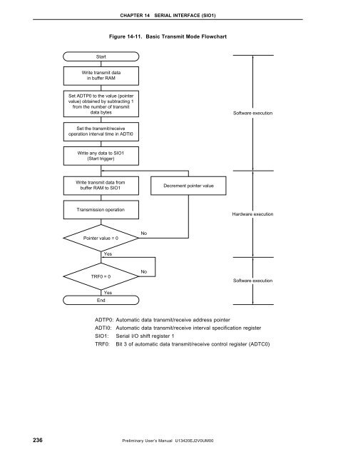
- Page 237: CHAPTER 14 SERIAL INTERFACE (SIO1)
- Page 241 and 242: CHAPTER 14 SERIAL INTERFACE (SIO1)
- Page 243 and 244: CHAPTER 14 SERIAL INTERFACE (SIO1)
- Page 245 and 246: SCK1 CHAPTER 14 SERIAL INTERFACE (S
- Page 247 and 248: SCK1 SO1 SI1 BUSY CSIIF1 TRF0 CHAPT
- Page 249 and 250: CHAPTER 14 SERIAL INTERFACE (SIO1)
- Page 251 and 252: CHAPTER 14 SERIAL INTERFACE (SIO1)
- Page 253 and 254: 15.1 Serial Interface (SIO30) Funct
- Page 255 and 256: CHAPTER 15 SERIAL INTERFACE (SIO30)
- Page 257 and 258: CHAPTER 15 SERIAL INTERFACE (SIO30)
- Page 259 and 260: 16.1 Serial Interface (SIO31) Funct
- Page 261 and 262: CHAPTER 16 SERIAL INTERFACE (SIO31)
- Page 263 and 264: CHAPTER 16 SERIAL INTERFACE (SIO31)
- Page 265 and 266: 17.1 Interrupt Function Types CHAPT
- Page 267 and 268: (A) Internal non-maskable interrupt
- Page 269 and 270: 17.3 Interrupt Function Control Reg
- Page 271 and 272: CHAPTER 17 INTERRUPT FUNCTIONS (2)
- Page 273 and 274: CHAPTER 17 INTERRUPT FUNCTIONS (4)
- Page 275 and 276: 17.4 Interrupt Servicing Operations
- Page 277 and 278: CHAPTER 17 INTERRUPT FUNCTIONS Figu
- Page 279 and 280: CHAPTER 17 INTERRUPT FUNCTIONS Figu
- Page 281 and 282: CHAPTER 17 INTERRUPT FUNCTIONS 17.4
- Page 283 and 284: CHAPTER 17 INTERRUPT FUNCTIONS Figu
- Page 285 and 286: CHAPTER 18 EXTERNAL DEVICE EXPANSIO
- Page 287 and 288: CHAPTER 18 EXTERNAL DEVICE EXPANSIO
- Page 289 and 290:
CHAPTER 18 EXTERNAL DEVICE EXPANSIO
- Page 291 and 292:
ASTB RD AD0 to AD7 A8 to A15 ASTB R
- Page 293 and 294:
ASTB RD WR AD0 to AD7 A8 to A15 AST
- Page 295 and 296:
19.1 Standby Function and Configura
- Page 297 and 298:
19.2 Standby Function Operations 19
- Page 299 and 300:
CHAPTER 19 STANDBY FUNCTION (c) Cle
- Page 301 and 302:
CHAPTER 19 STANDBY FUNCTION (2) STO
- Page 303 and 304:
20.1 Reset Function CHAPTER 20 RESE
- Page 305 and 306:
CHAPTER 20 RESET FUNCTION Table 20-
- Page 307 and 308:
CHAPTER 21 μPD78F0066 The μPD78F0
- Page 309 and 310:
CHAPTER 21 μPD78F0066 21.2 Interna
- Page 311 and 312:
CHAPTER 21 μPD78F0066 21.3.2 Flash
- Page 313 and 314:
CHAPTER 22 INSTRUCTION SET This cha
- Page 315 and 316:
CHAPTER 22 INSTRUCTION SET 22.1.2 D
- Page 317 and 318:
Instruction Group 16-bit data trans
- Page 319 and 320:
Instruction Group 8-bit operation C
- Page 321 and 322:
CHAPTER 22 INSTRUCTION SET Instruct
- Page 323 and 324:
CHAPTER 22 INSTRUCTION SET Instruct
- Page 325 and 326:
CHAPTER 22 INSTRUCTION SET Second O
- Page 327 and 328:
CHAPTER 22 INSTRUCTION SET (4) Call
- Page 329 and 330:
APPENDIX A DEVELOPMENT TOOLS The fo
- Page 331 and 332:
(2) When using the in-circuit emula
- Page 333 and 334:
APPENDIX A DEVELOPMENT TOOLS Remark
- Page 335 and 336:
A.3.1 Hardware (2/2) (2) When using
- Page 337 and 338:
A.3.2 Software (2/2) ID78K0-NS Inte
- Page 339 and 340:
APPENDIX A DEVELOPMENT TOOLS Conver
- Page 341 and 342:
APPENDIX B EMBEDDED SOFTWARE For ef
- Page 343 and 344:
Real-Time OS (2/2) APPENDIX B EMBED
- Page 345 and 346:
APPENDIX C REGISTER INDEX C.1 Regis
- Page 347 and 348:
16-bit timer/counter 0 (TM0) … 10
- Page 349 and 350:
[P] P0: Port 0 … 73 P2: Port 2
- Page 351 and 352:
The following shows major revisions
- Page 353:
Facsimile Message From: Name Compan