EUV mask cleaning challenges for 16 nm and 11 nm HP ... - ieuvi.org
EUV mask cleaning challenges for 16 nm and 11 nm HP ... - ieuvi.org
EUV mask cleaning challenges for 16 nm and 11 nm HP ... - ieuvi.org

Create successful ePaper yourself
Turn your PDF publications into a flip-book with our unique Google optimized e-Paper software.
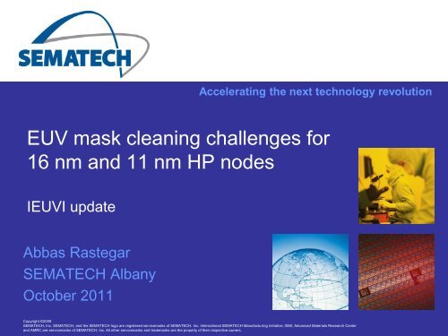
Accelerating the next technology revolution<br />
<strong>EUV</strong> <strong>mask</strong> <strong>cleaning</strong> <strong>challenges</strong> <strong>for</strong><br />
<strong>16</strong> <strong>nm</strong> <strong>and</strong> <strong>11</strong> <strong>nm</strong> <strong>HP</strong> nodes<br />
I<strong>EUV</strong>I update<br />
Abbas Rastegar<br />
SEMATECH Albany<br />
October 20<strong>11</strong><br />
Copyright ©2009<br />
SEMATECH, Inc. SEMATECH, <strong>and</strong> the SEMATECH logo are registered servicemarks of SEMATECH, Inc. International SEMATECH Manufacturing Initiative, ISMI, Advanced Materials Research Center<br />
<strong>and</strong> AMRC are servicemarks of SEMATECH, Inc. All other servicemarks <strong>and</strong> trademarks are the property of their respective owners.
Outline<br />
• Global issues of <strong>mask</strong> <strong>cleaning</strong><br />
• Cleaning Challenges of <strong>EUV</strong> <strong>mask</strong>s <strong>for</strong> 22-<strong>16</strong> <strong>nm</strong> <strong>HP</strong><br />
– Mask structure <strong>for</strong> <strong>16</strong> <strong>nm</strong> <strong>HP</strong><br />
– Choice of chemistries<br />
– Cleaning technologies<br />
– Material issues<br />
– Particle removal issues<br />
• Cleaning Challenges of <strong>EUV</strong> <strong>mask</strong>s <strong>for</strong> <strong>11</strong> <strong>nm</strong> <strong>HP</strong><br />
– <strong>EUV</strong> options <strong>for</strong> <strong>11</strong><strong>nm</strong> <strong>HP</strong> node<br />
– Mask structure <strong>for</strong> <strong>11</strong> <strong>nm</strong> <strong>HP</strong><br />
– Choice of materials<br />
– Material issues<br />
• Summary <strong>and</strong> conclusions<br />
26 October 20<strong>11</strong> SEMATECH Confidential<br />
2
Global issues of <strong>mask</strong> <strong>cleaning</strong><br />
• Mask <strong>cleaning</strong> suffers from general issues of the <strong>mask</strong><br />
industry concerning lack of resources<br />
– Dem<strong>and</strong>s <strong>for</strong> solutions <strong>for</strong> near time problems<br />
• Lack of inspection capability<br />
– Needed <strong>for</strong> end users ( patterned <strong>mask</strong>s in the fab)<br />
– Needed <strong>for</strong> tool development ( substrate, blank <strong>and</strong> patterned)<br />
– Needed <strong>for</strong> process development ( substrate, blank <strong>and</strong> patterned)<br />
• Lack of underst<strong>and</strong>ing of a printable particle.<br />
– Particle removal depends on size, shape, composition <strong>and</strong> location<br />
of defect<br />
• <strong>EUV</strong> surface materials not well established<br />
– Absorber, Arc <strong>and</strong> Capping layer composition <strong>and</strong> height changes<br />
• Few suppliers <strong>for</strong> <strong>mask</strong> <strong>cleaning</strong> tools<br />
– Small market size limit contribution of large clean tool suppliers<br />
• Lack of innovative solutions <strong>for</strong> the <strong>mask</strong> <strong>cleaning</strong><br />
26 October 20<strong>11</strong> SEMATECH Confidential<br />
3
Mask <strong>cleaning</strong> roadmap (long-term)<br />
Min defect size SEVD (<strong>nm</strong>)<br />
60<br />
50<br />
40<br />
30<br />
20<br />
10<br />
0<br />
ISMT Sustrate Substrate ISMT Blank/Mask ITRS Blank ITRS-Mask-SEVD<br />
ISMT 22 <strong>nm</strong> <strong>HP</strong> ISMT <strong>16</strong> <strong>nm</strong> <strong>HP</strong> ISMT <strong>11</strong> <strong>nm</strong> <strong>HP</strong><br />
2009 2010 20<strong>11</strong> 2012 2013 2014 2015 20<strong>16</strong> 2017 2018 2019 2020<br />
Year<br />
NA >0.5<br />
ISMT:SEMATECH<br />
SEVD <strong>for</strong> spherical<br />
defect calculated from<br />
absorber defect area<br />
Substrate defects will be<br />
smoothed by ML deposition<br />
• Cleaning tools <strong>and</strong> processes should be able to remove sub-10 <strong>nm</strong><br />
particles<br />
26 October 20<strong>11</strong> SEMATECH Confidential<br />
4
<strong>EUV</strong> <strong>mask</strong> structure <strong>and</strong> materials <strong>for</strong><br />
<strong>16</strong> <strong>nm</strong> <strong>HP</strong> ( 64 <strong>nm</strong> lines on <strong>mask</strong>)<br />
• Critical <strong>cleaning</strong> steps<br />
26 October 20<strong>11</strong><br />
• Substrate <strong>cleaning</strong><br />
• Ru-capped ML blank <strong>cleaning</strong><br />
• Patterned <strong>EUV</strong> <strong>mask</strong> <strong>cleaning</strong><br />
• Materials in contact with chemistry<br />
SEMATECH Confidential<br />
ARC<br />
Absorber Stack<br />
Capping layer<br />
Multilayers<br />
LTEM substrate<br />
Conductive<br />
backside layer<br />
• Ti-doped fused silica, Ru, MoSi, CrN, TaNO/TaBO, SiON<br />
• Surface requirements:<br />
• Substrate : roughness 80 pm, flatness 50 <strong>nm</strong> PV<br />
• MoSi Ru-capped blank: roughness 100 pm, flatness 50 <strong>nm</strong> PV<br />
~ 7-15 <strong>nm</strong> thick<br />
HfO 10 <strong>nm</strong><br />
~ 50 - 75 <strong>nm</strong> thick<br />
TaBO/TaBN,<br />
TaNO/TaN<br />
~ 2-4 <strong>nm</strong> thick<br />
2.5 <strong>nm</strong> Ru,<br />
4 <strong>nm</strong> Si<br />
~ 250-350 <strong>nm</strong> thick<br />
MoSi(3 <strong>nm</strong>/4 <strong>nm</strong>)<br />
40 to 50 pairs<br />
Ti-doped fused silica<br />
~ 6.4 mm thick<br />
CrN<br />
70-100 <strong>nm</strong> thick<br />
5
Current <strong>challenges</strong> of <strong>cleaning</strong> <strong>EUV</strong><br />
<strong>mask</strong>s<br />
During <strong>mask</strong> manufacturing<br />
– Post CMP <strong>cleaning</strong><br />
– Substrate <strong>cleaning</strong><br />
• Removal of 10 <strong>nm</strong> particles<br />
• Cleaning-induced pits<br />
• Sub-10 <strong>nm</strong> particle adders<br />
– Ru-capped ML blank <strong>cleaning</strong><br />
• <strong>EUV</strong> reflectivity loss<br />
• Cleaning induced pits<br />
• Sub-30 <strong>nm</strong> particle adders<br />
• Surface contamination<br />
– Patterned <strong>EUV</strong> <strong>mask</strong>s<br />
• Sub-30 <strong>nm</strong> particle removal from<br />
contacts <strong>and</strong> trenches<br />
• Ru oxidation/removal<br />
• Absorber <strong>and</strong> ARC etch<br />
SEMATECH Confidential<br />
During <strong>mask</strong> repetitive use<br />
– Material <strong>challenges</strong><br />
• Ru cap oxidation <strong>and</strong> etch<br />
• Ru contamination<br />
• Absorber etch <strong>and</strong> change of CD<br />
• CrN durability<br />
– Particle removal <strong>challenges</strong><br />
• Sub-30 <strong>nm</strong> particle removal from<br />
contacts <strong>and</strong> trenches<br />
• Sub-30 <strong>nm</strong> particle adders<br />
• Cleaning-induced pits<br />
– Lifetime <strong>and</strong> storage <strong>challenges</strong><br />
• Progressive defects<br />
• <strong>EUV</strong> reflectivity loss<br />
• Surface contamination<br />
26 October 20<strong>11</strong> 6
Cleaning technology choices <strong>for</strong> <strong>EUV</strong><br />
<strong>mask</strong>s<br />
• Surface conditioning<br />
– Optical<br />
• VUV (172 <strong>nm</strong>) in gas atmosphere<br />
• In situ UV in solution<br />
– Chemical<br />
• SPM<br />
• Particle removal<br />
– Megasonic ( ~ 900 KHz � 4 MHz)<br />
• Used by all <strong>mask</strong> <strong>and</strong> wafer <strong>cleaning</strong> tools<br />
• Nozzle configuration or proximity flat transducers<br />
– Spray (low speed to high speed jets)<br />
• Used by all <strong>mask</strong> <strong>and</strong> wafer <strong>cleaning</strong> tools<br />
• Liquid or gas/liquid sprays<br />
– Cryogenic (CO 2, Ar)<br />
• Drying<br />
– Spin dry<br />
– Marongoni-based<br />
Surface<br />
conditioning<br />
VUV(173<strong>nm</strong>)<br />
N2/O2<br />
Out of box <strong>cleaning</strong> ideas are needed <strong>for</strong> <strong>EUV</strong><br />
No new chemistry has been introduced <strong>for</strong> <strong>EUV</strong><br />
SEMATECH Confidential<br />
Organic/<br />
particle<br />
removal<br />
O3/APM<br />
, SPM<br />
Particle<br />
removal<br />
APM<br />
+1MHz<br />
26 October 20<strong>11</strong> 7<br />
No Conditioning<br />
with Conditioning<br />
Rinse Dry<br />
DI<br />
rinse<br />
Spin<br />
Dry
Substrate<br />
Challenges of substrate <strong>cleaning</strong>:<br />
Pits, PRE, adders<br />
Megasonic<br />
Nozzle<br />
Impact<br />
Area<br />
Area scanned<br />
by nozzle<br />
SEMATECH Confidential<br />
100X <strong>cleaning</strong><br />
30 <strong>nm</strong> inspection 50 <strong>nm</strong> inspection<br />
• For sub-30 <strong>nm</strong> defects current <strong>cleaning</strong> processes have low PRE,<br />
create pits, <strong>and</strong> generate non-detectable particles (~ 4 <strong>nm</strong> high)<br />
A. Rastegar<br />
26 October 20<strong>11</strong> 8<br />
Count<br />
20<br />
18<br />
<strong>16</strong><br />
14<br />
12<br />
10<br />
8<br />
6<br />
4<br />
2<br />
0<br />
Particle Height<br />
1 2 3 4 5 More<br />
Height (<strong>nm</strong>)
Frontside<br />
Backside<br />
Challenges of Ru cap multilayer <strong>cleaning</strong>:<br />
Adders, pits, PRE,<br />
• Many particles on top surface are embedded<br />
• Particles added by the <strong>cleaning</strong> are an issue<br />
• Removal of backside metallic particles is challenging<br />
26 October 20<strong>11</strong> SEMATECH Confidential<br />
9
Particle removal <strong>challenges</strong>:<br />
Megasonic induced pits on Ru<br />
After 40X <strong>cleaning</strong><br />
(1 MHz,3MHz)<br />
• Some megasonic induced pits are printable ( H. Kwon- BACUS 20<strong>11</strong>)<br />
26 October 20<strong>11</strong> SEMATECH Confidential<br />
10
How many times an <strong>EUV</strong> <strong>mask</strong> be cleaned?<br />
• <strong>EUV</strong> reflectivity (R max) dropped below spec after 20X <strong>cleaning</strong><br />
• What is the mechanism of <strong>EUV</strong> reflectivity loss?<br />
SEMATECH Confidential<br />
±0.5%<br />
<strong>EUV</strong>L presentation on Tuesday<br />
26 October 20<strong>11</strong> <strong>11</strong>
Material issues: Ru<br />
Ru cap contamination<br />
Adder count<br />
100<br />
Accumulated Time(min) adders (P4+) inspected by M1350<br />
26 October 20<strong>11</strong> SEMATECH Confidential<br />
12<br />
80<br />
60<br />
40<br />
20<br />
0<br />
RuSTD38 in N2<br />
RuSTD38 in air<br />
RuH238 in N2<br />
RuH238 in air<br />
Ru act as a getter <strong>and</strong> very fast get contaminated<br />
Contact angle (degree)<br />
60<br />
50<br />
40<br />
30<br />
20<br />
10<br />
0<br />
VUV+Ar 2<br />
VUV+N2<br />
0 3 4 6 7 8 10 20 22 <strong>16</strong> 30 90 210 1440<br />
Recipe APM-N2<br />
Recipe APM-Air<br />
Recipe H2DI-N2<br />
Recipe H2Di-Air<br />
Particle adders<br />
0 1 3 5 9 13 19 30<br />
Aging date (days)
<strong>EUV</strong> <strong>mask</strong> durability to pattern damage<br />
Removal <strong>for</strong>ce (uN)<br />
<strong>16</strong><br />
14<br />
12<br />
10<br />
8<br />
6<br />
4<br />
2<br />
0<br />
Breakage<br />
<strong>for</strong>ce<br />
W100<strong>nm</strong><br />
H80<strong>nm</strong><br />
Process<br />
Window<br />
SiO2<br />
100<strong>nm</strong><br />
SiO2<br />
50<strong>nm</strong><br />
PSL<br />
100<strong>nm</strong><br />
Same day<br />
2 days<br />
8 days<br />
Removal <strong>for</strong>ce<br />
PSL<br />
50<strong>nm</strong><br />
• <strong>EUV</strong> <strong>mask</strong>s are less prone to pattern damage by megasonics<br />
thantheir optical counter parts<br />
Shimomura et al., SPCC<strong>11</strong>, BACUS <strong>11</strong><br />
26 October 20<strong>11</strong> SEMATECH Confidential<br />
13
Cleaning <strong>challenges</strong> of <strong>EUV</strong> patterned <strong>mask</strong>s:<br />
TaN absorber etch by SPM<br />
After 28 <strong>nm</strong> SiO2 deposition After multiple SPM+MS <strong>cleaning</strong><br />
• 28 <strong>nm</strong> SiO 2 particles were removed by SPM <strong>cleaning</strong> process<br />
• TaN absorber line got etched, CD increased, LER reduced<br />
SEMATECH Confidential
Particle removal <strong>challenges</strong>: flow<br />
Only MS<br />
Rotational flow + MS<br />
PRE( %)<br />
26 October 20<strong>11</strong> SEMATECH Confidential<br />
15<br />
10 0<br />
90<br />
80<br />
70<br />
60<br />
50<br />
40<br />
30<br />
20<br />
10<br />
0<br />
Rotational flow + MS<br />
8 0 <strong>nm</strong> 10 0 <strong>nm</strong> 150 <strong>nm</strong> CT<br />
No plate rotation<br />
Megasonics cannot remove particles without flow close to surface<br />
SC1<br />
POR<br />
Only MS<br />
Pattern width 80 <strong>nm</strong> 100 <strong>nm</strong> 150 <strong>nm</strong> 100 <strong>nm</strong><br />
contact
Particle removal <strong>challenges</strong><br />
Metallic particles<br />
• Current <strong>cleaning</strong> process do NOT<br />
remove metals<br />
• Native metal particles are not<br />
removed<br />
• Most Deposited particle metals are<br />
removable<br />
DI rinse<br />
SC1 18 min<br />
SC1 40 min<br />
O3+SC1<br />
SEMATECH Confidential<br />
26 October 20<strong>11</strong> <strong>16</strong>
<strong>EUV</strong> options <strong>for</strong> <strong>11</strong> <strong>nm</strong> <strong>HP</strong><br />
• Reduce the wavelength<br />
– Xe� ~ <strong>11</strong> <strong>nm</strong><br />
• no real advantage<br />
– Sn� 6.8 <strong>nm</strong><br />
• Almost ½ intensity of 13.5 <strong>nm</strong><br />
• Requires high power source<br />
– <strong>EUV</strong> blank film structure<br />
should change( G )<br />
• Increase NA<br />
– Impact s <strong>mask</strong> structure <strong>and</strong><br />
materials<br />
• Reduce the K 1<br />
– Tool dependent<br />
SEMATECH Confidential<br />
Emission spectra of tin plasma<br />
6.8<strong>nm</strong><br />
13.5 <strong>nm</strong><br />
<strong>EUV</strong> sources by V. Bakshi<br />
26 October 20<strong>11</strong> 17
Materials choices <strong>for</strong> <strong>11</strong> <strong>nm</strong> <strong>HP</strong> node<br />
Index of refraction at l= 13.5 <strong>nm</strong><br />
Mask shadowing effects requires thin absorber<br />
Thinner absorber requires higher absorption<br />
C<strong>and</strong>idate<br />
materials<br />
26 October 20<strong>11</strong> SEMATECH Confidential<br />
18
Challenges of <strong>cleaning</strong> <strong>for</strong> <strong>11</strong> <strong>nm</strong> <strong>HP</strong><br />
<strong>EUV</strong> <strong>mask</strong>s<br />
• Assuming <strong>EUV</strong> wavelength remain 13.5 <strong>nm</strong><br />
– NA� >0.5 � 8 mirrors optics� Chief Ray Angle � >10<br />
– MoSi � Multi stack with different periodicity � impacts blank defectivity<br />
– ML deposition processes smooth sub 10 <strong>nm</strong> substrate pits<br />
– There should be no megasonic induced pits >10 <strong>nm</strong><br />
• ARC materials<br />
– Actinic inspection requires new materials (Ni,Pt,Cu,..)<br />
• Absorber layer<br />
– New materials (Ni,Pt,Cu,..)<br />
• Capping layer<br />
– New materials ( TiO2, V2O5, Ru, Ta,..)<br />
– Depends on choice of absorber, Arc, <strong>and</strong> availability of selective absorber<br />
etch processes<br />
SEMATECH Confidential<br />
26 October 20<strong>11</strong> 19
Summary <strong>and</strong> Conclusions-1<br />
• Substrate <strong>cleaning</strong><br />
– Substrate defectivity is responsible <strong>for</strong> about 80% of the blank defects<br />
– Lack of inspection capability below 20 <strong>nm</strong> is the most critical<br />
challenge <strong>for</strong> progress in substrate <strong>cleaning</strong><br />
– No <strong>cleaning</strong> technology is available <strong>for</strong> 10 <strong>nm</strong> particle removal<br />
– To reduce particle adders sub 10 <strong>nm</strong> filtration of chemicals <strong>and</strong> DI<br />
water with proper flow rate is required but currently is not available<br />
– None of the smoothing techniques have been as successful as CMP<br />
( SEMATECH poster in <strong>EUV</strong>L)<br />
– LTEM CMP is the most critical step in manufacturing <strong>EUV</strong> <strong>mask</strong><br />
substrates (impacts defects, roughness, flatness, surface hardness).<br />
Very limited resources work on <strong>EUV</strong> substrate CMP!!<br />
– Post CMP <strong>cleaning</strong> processes need to be optimized together with<br />
final <strong>cleaning</strong> processes.( Complementary processes)<br />
– Backside CrN deposition process can impact LTEM front side<br />
defectivity<br />
SEMATECH Confidential<br />
26 October 20<strong>11</strong> 20
Summary <strong>and</strong> Conclusions-2<br />
• Patterned <strong>EUV</strong> <strong>mask</strong> <strong>cleaning</strong><br />
– Currently there is not enough data <strong>for</strong> the size <strong>and</strong> composition of<br />
printable particles on top of <strong>EUV</strong> <strong>mask</strong>s<br />
– Absorber <strong>and</strong> ARC etch by oxidizing chemistries is a challenge<br />
– Removal of sub 30 <strong>nm</strong> particles from inside of trenches <strong>and</strong> contact<br />
holes <strong>for</strong> <strong>16</strong> <strong>nm</strong> <strong>HP</strong> is a challenge<br />
– <strong>EUV</strong> reflectivity loss by multiple <strong>cleaning</strong> is challenging<br />
– Pit induced by the <strong>cleaning</strong> on Ru surface is an issue but no pit<br />
defects have been detected on the patterned <strong>EUV</strong> <strong>mask</strong>s (Lack of<br />
inspection capability?)<br />
• Mask <strong>cleaning</strong> at <strong>11</strong> <strong>nm</strong> <strong>HP</strong> node<br />
– Many materials are still unknown. However SEMATECH has started<br />
<strong>cleaning</strong> feasibility studies of potential materials<br />
– There is a need <strong>for</strong> collaboration among all surface <strong>cleaning</strong><br />
communities <strong>for</strong> tackling <strong>EUV</strong> <strong>mask</strong> <strong>cleaning</strong> issues. SEMATECH<br />
supports such collaborations<br />
SEMATECH Confidential<br />
26 October 20<strong>11</strong> 21
Thank You<br />
26 October 20<strong>11</strong> SEMATECH Confidential<br />
22
Chemistry choices <strong>for</strong> <strong>EUV</strong> <strong>mask</strong>s<br />
• Traditional chemistries are still in use <strong>for</strong> <strong>mask</strong> <strong>cleaning</strong><br />
– SPM ( H 2SO 4/H 2O 2) ( 8�5:1)<br />
– APM ( NH 4OH/H 2O 2/H 2O) ( 1:1:5�8)<br />
– O 3 based (O 3/H 2O) , (O 3/APM) ( O 3 :6� 50 ppm)<br />
– H 2 based (H 2/H 2O) , (H 2/NH 4OH) ( 1� 1.4 ppm)<br />
– Dilute Ammonia (H 2O/NH 4OH) ( 1� 6 ppm)<br />
– Clustered water (H 2O/NH 4OH)<br />
• <strong>HP</strong>M ( HCl/H 2O 2/H 2O) , Dilute HF is NOT used due to many<br />
metallic surfaces in <strong>EUV</strong> <strong>mask</strong>s<br />
• Solvents are not used due to risk of progressive defects<br />
<strong>and</strong> (optical induced) haze observed in optical <strong>mask</strong>s<br />
• No new chemistry has been introduced <strong>for</strong> <strong>EUV</strong><br />
SEMATECH Confidential<br />
26 October 20<strong>11</strong> 23
Requirement of ML structure change<br />
<strong>for</strong> NA>0.5<br />
Source Zeiss-Bacus 2010<br />
NA=0.45, CRA=8<br />
=CRA<br />
In CRA><strong>11</strong>,Na >0.5<br />
<strong>EUV</strong> reflectivity will<br />
drop<br />
ML structure should<br />
change<br />
26 October 20<strong>11</strong> SEMATECH Confidential<br />
24
Impact of <strong>EUV</strong> @ NA>0.5 on <strong>mask</strong><br />
Source: Ruoff- Zeiss-Bacus 2010<br />
<strong>11</strong> <strong>nm</strong><br />
• New absorber material <strong>and</strong> multilayer structure will have impact on<br />
choice of the <strong>cleaning</strong> chemistries<br />
26 October 20<strong>11</strong> SEMATECH Confidential<br />
25