

Two-wire Serial EEPROM AT24C1024(1) - Atmel Corporation
Two-wire Serial EEPROM AT24C1024(1) - Atmel Corporation
Two-wire Serial EEPROM AT24C1024(1) - Atmel Corporation

Create successful ePaper yourself
Turn your PDF publications into a flip-book with our unique Google optimized e-Paper software.
Features<br />
• Low-voltage Operation<br />
– 2.7 (V CC = 2.7V to 5.5V)<br />
• Internally Organized 131,072 x 8<br />
• <strong>Two</strong>-<strong>wire</strong> <strong>Serial</strong> Interface<br />
• Schmitt Triggers, Filtered Inputs for Noise Suppression<br />
• Bidirectional Data Transfer Protocol<br />
• 400 kHz (2.7V) and 1 MHz (5V) Clock Rate<br />
• Write Protect Pin for Hardware and Software Data Protection<br />
• 256-byte Page Write Mode (Partial Page Writes Allowed)<br />
• Random and Sequential Read Modes<br />
• Self-timed Write Cycle (5 ms Typical)<br />
• High Reliability<br />
– Endurance: 100,000 Write Cycles/Page<br />
– Data Retention: 40 Years<br />
• 8-lead PDIP, 8-lead EIAJ SOIC, 8-lead LAP and 8-lead SAP Packages<br />
• Die Sales: Wafer Form, Waffle Pack and Bumped Die<br />
Description<br />
The <strong>AT24C1024</strong> provides 1,048,576 bits of serial electrically erasable and programmable<br />
read only memory (<strong>EEPROM</strong>) organized as 131,072 words of 8 bits each. The<br />
device’s cascadable feature allows up to two devices to share a common two-<strong>wire</strong><br />
bus. The device is optimized for use in many industrial and commercial applications<br />
where low-power and low-voltage operation are essential. The devices are available<br />
in space-saving 8-lead PDIP, 8-lead EIAJ SOIC, 8-lead Leadless Array (LAP) and 8lead<br />
SAP packages. In addition, the entire family is available in 2.7V (2.7V to 5.5V)<br />
versions.<br />
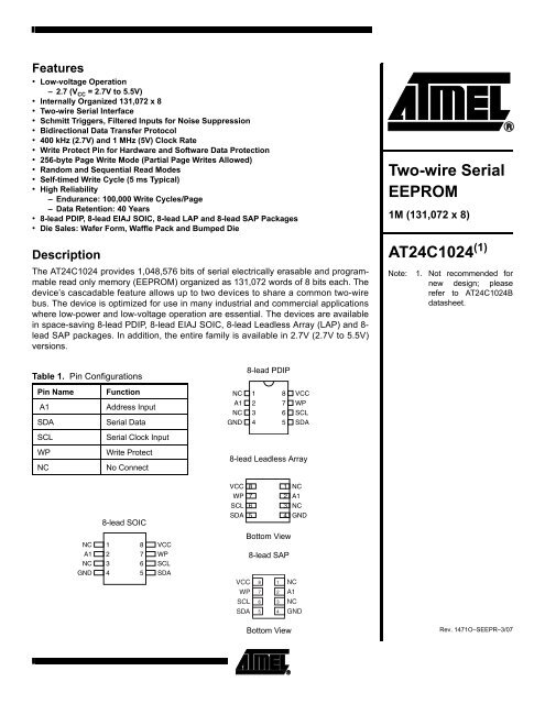
Table 1. Pin Configurations<br />
Pin Name Function<br />
A1 Address Input<br />
SDA <strong>Serial</strong> Data<br />
SCL <strong>Serial</strong> Clock Input<br />
WP Write Protect<br />
NC No Connect<br />
NC<br />
A1<br />
NC<br />
GND<br />
8-lead SOIC<br />
1<br />
2<br />
3<br />
4<br />
8<br />
7<br />
6<br />
5<br />
VCC<br />
WP<br />
SCL<br />
SDA<br />
NC<br />
A1<br />
NC<br />
GND<br />
8-lead PDIP<br />
1<br />
2<br />
3<br />
4<br />
8<br />
7<br />
6<br />
5<br />
VCC<br />
WP<br />
SCL<br />
SDA<br />
8-lead Leadless Array<br />
VCC<br />
WP<br />
SCL<br />
SDA<br />
8<br />
7<br />
6<br />
5<br />
VCC<br />
WP<br />
SCL<br />
SDA<br />
1<br />
2<br />
3<br />
4<br />
Bottom View<br />
8-lead SAP<br />
8<br />
7<br />
6<br />
5<br />
1<br />
2<br />
3<br />
4<br />
Bottom View<br />
NC<br />
A1<br />
NC<br />
GND<br />
NC<br />
A1<br />
NC<br />
GND<br />
<strong>Two</strong>-<strong>wire</strong> <strong>Serial</strong><br />
<strong>EEPROM</strong><br />
1M (131,072 x 8)<br />
<strong>AT24C1024</strong> (1)<br />
Note: 1. Not recommended for<br />
new design; please<br />
refer to <strong>AT24C1024</strong>B<br />
datasheet.<br />
Rev. 1471O–SEEPR–3/07<br />
1
Absolute Maximum Ratings*<br />
Operating Temperature..................................–55°C to +125°C *NOTICE: Stresses beyond those listed under “Absolute<br />
Storage Temperature .....................................–65°C to +150°C<br />
Voltage on Any Pin<br />
with Respect to Ground ....................................–1.0V to +7.0V<br />
Maximum Operating Voltage .......................................... 6.25V<br />
DC Output Current........................................................ 5.0 mA<br />
Figure 1. Block Diagram<br />
2 <strong>AT24C1024</strong><br />
Maximum Ratings” may cause permanent damage<br />
to the device. This is a stress rating only and<br />
functional operation of the device at these or any<br />
other conditions beyond those indicated in the<br />
operational sections of this specification is not<br />
implied. Exposure to absolute maximum rating<br />
conditions for extended periods may affect<br />
device reliability.<br />
1471O–SEEPR–3/07
1471O–SEEPR–3/07<br />
<strong>AT24C1024</strong><br />
Pin Description SERIAL CLOCK (SCL): The SCL input is used to positive edge clock data into each<br />
<strong>EEPROM</strong> device and negative edge clock data out of each device.<br />
SERIAL DATA (SDA): The SDA pin is bi-directional for serial data transfer. This pin is opendrain<br />
driven and may be <strong>wire</strong>-ORed with any number of other open-drain or open-collector<br />
devices.<br />
DEVICE/ADDRESSES (A1): The A1 pin is a device address input that can be hard<strong>wire</strong>d or<br />
left not connected for hardware compatibility with other AT24Cxx devices. When the A1 pin is<br />
hard<strong>wire</strong>d, as many as two 1024K devices may be addressed on a single bus system (device<br />
addressing is discussed in detail under the Device Addressing section). If the A1 pin is left<br />
floating, the A1 pin will be internally pulled down to GND if the capacitive coupling to the circuit<br />
board VCC plane is 3 pF, <strong>Atmel</strong> recommends connecting the A1 pin to<br />
GND.<br />
WRITE PROTECT (WP): The write protect input, when connected to GND, allows normal<br />
write operations. When WP is connected high to VCC , all write operations to the memory are<br />
inhibited. If the pin is left floating, the WP pin will be internally pulled down to GND if the<br />
capacitive coupling to the circuit board VCC plane is 3 pF, <strong>Atmel</strong> recommends<br />
connecting the pin to GND. Switching WP to VCC prior to a write operation creates a<br />
software write-protect function.<br />
Memory<br />
Organization<br />
<strong>AT24C1024</strong>, 1024K SERIAL <strong>EEPROM</strong>: The 1024K is internally organized as 512 pages of<br />
256 bytes each. Random word addressing requires a 17-bit data word address.<br />
3
Table 2. Pin Capacitance (1)<br />
Applicable over recommended operating range from T A = 25°C, f = 1.0 MHz, V CC = +2.7V<br />
Symbol Test Condition Max Units Conditions<br />
C I/O Input/Output Capacitance (SDA) 8 pF V I/O = 0V<br />
CIN Input Capacitance (A1 , SCL) 6 pF VIN = 0V<br />
Note: 1. This parameter is characterized and is not 100% tested.<br />
Table 3. DC Characteristics<br />
Applicable over recommended operating range from: TAI = –40°C to +85°C, VCC = +2.7V to +5.5V, TAC = 0°C to +70°C,<br />
VCC = +2.7V to +5.5V (unless otherwise noted)<br />
Symbol Parameter Test Condition Min Typ Max Units<br />
V CC Supply Voltage 2.7 5.5 V<br />
I CC Supply Current V CC = 5.0V READ at 400 kHz 2.0 mA<br />
I CC Supply Current V CC = 5.0V WRITE at 400 kHz 5.0 mA<br />
I SB<br />
Standby Current<br />
Note: 1. V IL min and V IH max are reference only and are not tested.<br />
4 <strong>AT24C1024</strong><br />
V CC = 2.7V V IN = V CC or V SS 3.0 µA<br />
V CC = 5.5V 6.0 µA<br />
ILI Input Leakage Current VIN = VCC or VSS 0.10 3.0 µA<br />
ILO Output Leakage<br />
Current<br />
VOUT = VCC or VSS 0.05 3.0 µA<br />
VIL Input Low Level (1)<br />
–0.6 VCC x 0.3 V<br />
Input High Level (1)<br />
VCC x 0.7 VCC + 0.5 V<br />
V IH<br />
V OL Output Low Level V CC = 3.0V I OL = 2.1 mA 0.4 V<br />
1471O–SEEPR–3/07
1471O–SEEPR–3/07<br />
<strong>AT24C1024</strong><br />
Table 4. AC Characteristics (1)<br />
Applicable over recommended operating range from TA = –40°C to +85°C, VCC = +2.7V to +5.5V, CL = 100 pF (unless<br />
otherwise noted)<br />
Symbol Parameter Test Conditions Min Max Units<br />
f SCL<br />
t LOW<br />
t HIGH<br />
t AA<br />
t BUF<br />
t HD.STA<br />
t SU.STA<br />
Clock Frequency, SCL<br />
Clock Pulse Width Low<br />
Clock Pulse Width High<br />
Clock Low to Data Out Valid<br />
Time the bus must be free before a new<br />
transmission can start (2)<br />
Start Hold Time<br />
Start Setup Time<br />
4.5V ≤ V CC ≤ 5.5V<br />
2.7V ≤ V CC ≤ 5.5V<br />
4.5V ≤ V CC ≤ 5.5V<br />
2.7V ≤ V CC ≤ 5.5V<br />
4.5V ≤ V CC ≤ 5.5V<br />
2.7V ≤ V CC ≤ 5.5V<br />
4.5V ≤ V CC ≤ 5.5V<br />
2.7V ≤ V CC ≤ 5.5V<br />
4.5V ≤ V CC ≤ 5.5V<br />
2.7V ≤ V CC ≤ 5.5V<br />
4.5V ≤ V CC ≤ 5.5V<br />
2.7V ≤ V CC ≤ 5.5V<br />
4.5V ≤ V CC ≤ 5.5V<br />
2.7V ≤ V CC ≤ 5.5V<br />
tHD.DAT Data In Hold Time 0 µs<br />
tSU.DAT Data In Setup Time 100 ns<br />
tR Inputs Rise Time (2)<br />
0.3 µs<br />
tF Inputs Fall Time (2) 4.5V ≤ VCC ≤ 5.5V<br />
2.7V ≤ VCC ≤ 5.5V<br />
100<br />
300<br />
ns<br />
t SU.STO<br />
Stop Setup Time<br />
4.5V ≤ V CC ≤ 5.5V<br />
2.7V ≤ V CC ≤ 5.5V<br />
t DH Data Out Hold Time 50 ns<br />
t WR Write Cycle Time 10 ms<br />
Endurance (2)<br />
5.0V, 25°C, Page Mode 100K Write Cycles<br />
Notes: 1. AC measurement conditions:<br />
RL (connects to VCC): 1.3 kΩ (2.7V, 5V)<br />
Input pulse voltages: 0.3 VCC to 0.7 VCC Input rise and fall times: ≤50 ns<br />
Input and output timing reference voltages: 0.5 VCC 2. This parameter is ensured by characterization only.<br />
0.4<br />
1.3<br />
0.4<br />
0.6<br />
0.05<br />
0.05<br />
0.5<br />
1.3<br />
0.25<br />
0.6<br />
0.25<br />
0.6<br />
0.25<br />
0.6<br />
1000<br />
400<br />
0.55<br />
0.9<br />
kHz<br />
µs<br />
µs<br />
µs<br />
µs<br />
µs<br />
µs<br />
µs<br />
5
Device<br />
Operation<br />
6 <strong>AT24C1024</strong><br />
CLOCK and DATA TRANSITIONS: The SDA pin is normally pulled high with an external<br />
device. Data on the SDA pin may change only during SCL low time periods (see Figure 4 on<br />
page 7). Data changes during SCL high periods will indicate a start or stop condition as<br />
defined below.<br />
START CONDITION: A high-to-low transition of SDA with SCL high is a start condition which<br />
must precede any other command (see Figure 5 on page 8).<br />
STOP CONDITION: A low-to-high transition of SDA with SCL high is a stop condition. After a<br />
read sequence, the Stop command will place the <strong>EEPROM</strong> in a standby power mode (see<br />
Figure 5 on page 8).<br />
ACKNOWLEDGE: All addresses and data words are serially transmitted to and from the<br />
<strong>EEPROM</strong> in 8-bit words. The <strong>EEPROM</strong> sends a zero during the ninth clock cycle to acknowledge<br />
that it has received each word.<br />
STANDBY MODE: The <strong>AT24C1024</strong> features a low-power standby mode which is enabled: a)<br />
upon power-up and b) after the receipt of the stop bit and the completion of any internal<br />
operations.<br />
MEMORY RESET: After an interruption in protocol, power loss or system reset, any two-<strong>wire</strong><br />
part can be reset by following these steps:<br />
1. Clock up to 9 cycles.<br />
2. Look for SDA high in each cycle while SCL is high.<br />
3. Create a start condition.<br />
Device Power Up And Power Down Recommendation<br />
POWER UP: It is recommended to power up from 0V to full VCC in less than 1ms and then<br />
hold for at least 100µs at full VCC level before first operation.<br />
POWER DOWN: It is recommended to power down from full VCC to 0V in less than 1ms and<br />
then hold at 0V for at least 0.5s before power up. It is not recommended to VCC power down<br />
to non-zero volt and then slowly go to zero volt.<br />
1471O–SEEPR–3/07
Figure 2. Bus Timing (SCL: <strong>Serial</strong> Clock, SDA: <strong>Serial</strong> Data I/O ® )<br />
Figure 3. Write Cycle Timing (SCL: <strong>Serial</strong> Clock, SDA: <strong>Serial</strong> Data I/O)<br />
SCL<br />
SDA<br />
1471O–SEEPR–3/07<br />
WORDn<br />
<strong>AT24C1024</strong><br />
Note: 1. The write cycle time t WR is the time from a valid stop condition of a write sequence to the end of the internal clear/write cycle.<br />
Figure 4. Data Validity<br />
8th BIT<br />
ACK<br />
STOP<br />
CONDITION<br />
t wr (1)<br />
START<br />
CONDITION<br />
7
Figure 5. Start and Stop Definition<br />
Figure 6. Output Acknowledge<br />
Device<br />
Addressing<br />
8 <strong>AT24C1024</strong><br />
The 1024K <strong>EEPROM</strong> requires an 8-bit device address word following a start condition to<br />
enable the chip for a read or write operation (see Figure 7 on page 11). The device address<br />
word consists of a mandatory one, zero sequence for the first five most significant bits as<br />
shown. This is common to all two-<strong>wire</strong> <strong>EEPROM</strong> devices.<br />
The 1024K uses the one device address bit, A1, to allow up to two devices on the same bus.<br />
The A1 bit must compare to the corresponding hard<strong>wire</strong>d input pin. The A1 pin uses an internal<br />
proprietary circuit that biases it to a logic low condition if the pin is allowed to float.<br />
The seventh bit (P0 ) of the device address is a memory page address bit. This memory page<br />
address bit is the most significant bit of the data word address that follows. The eighth bit of<br />
the device address is the read/write operation select bit. A read operation is initiated if this bit<br />
is high and a write operation is initiated if this bit is low.<br />
Upon a compare of the device address, the <strong>EEPROM</strong> will output a zero. If a compare is not<br />
made, the device will return to a standby state.<br />
DATA SECURITY: The <strong>AT24C1024</strong> has a hardware data protection scheme that allows the<br />
user to write-protect the entire memory when the WP pin is at V CC .<br />
1471O–SEEPR–3/07
Write<br />
Operations<br />
1471O–SEEPR–3/07<br />
<strong>AT24C1024</strong><br />
BYTE WRITE: To select a data word in the 1024K memory requires a 17-bit word address.<br />
The word address field consists of the P0 bit of the device address, then the most significant<br />
word address followed by the least significant word address (see Figure 8 on page 11)<br />
A write operation requires the P0 bit and two 8-bit data word addresses following the device<br />
address word and acknowledgment. Upon receipt of this address, the <strong>EEPROM</strong> will again<br />
respond with a zero and then clock in the first 8-bit data word. Following receipt of the 8-bit<br />
data word, the <strong>EEPROM</strong> will output a zero. The addressing device, such as a microcontroller,<br />
then must terminate the write sequence with a stop condition. At this time the <strong>EEPROM</strong> enters<br />
an internally timed write cycle, TWR , to the nonvolatile memory. All inputs are disabled during<br />
this write cycle and the <strong>EEPROM</strong> will not respond until the write is complete (see Figure 8 on<br />
page 11).<br />
PAGE WRITE: The 1024K <strong>EEPROM</strong> is capable of 256-byte page writes.<br />
A page write is initiated the same way as a byte write, but the microcontroller does not send a<br />
stop condition after the first data word is clocked in. Instead, after the <strong>EEPROM</strong> acknowledges<br />
receipt of the first data word, the microcontroller can transmit up to 255 more data words. The<br />
<strong>EEPROM</strong> will respond with a zero after each data word received. The microcontroller must terminate<br />
the page write sequence with a stop condition (see Figure 9 on page 11).<br />
The data word address lower 8 bits are internally incremented following the receipt of each<br />
data word. The higher data word address bits are not incremented, retaining the memory page<br />
row location. When the word address, internally generated, reaches the page boundary, the<br />
following byte is placed at the beginning of the same page. If more than 256 data words are<br />
transmitted to the <strong>EEPROM</strong>, the data word address will “roll over” and previous data will be<br />
overwritten. The address “rollover” during write is from the last byte of the current page to the<br />
first byte of the same page.<br />
ACKNOWLEDGE POLLING: Once the internally timed write cycle has started and the<br />
<strong>EEPROM</strong> inputs are disabled, acknowledge polling can be initiated. This involves sending a<br />
start condition followed by the device address word. The read/write bit is representative of the<br />
operation desired. Only if the internal write cycle has completed will the <strong>EEPROM</strong> respond<br />
with a zero, allowing the read or write sequence to continue.<br />
9
Read<br />
Operations<br />
10 <strong>AT24C1024</strong><br />
Read operations are initiated the same way as write operations with the exception that the<br />
read/write select bit in the device address word is set to one. There are three read operations:<br />
current address read, random address read and sequential read.<br />
CURRENT ADDRESS READ: The internal data word address counter maintains the last<br />
address accessed during the last read or write operation, incremented by one. This address<br />
stays valid between operations as long as the chip power is maintained. The address “rollover”<br />
during read is from the last byte of the last memory page, to the first byte of the first page.<br />
Once the device address with the read/write select bit set to one is clocked in and acknowledged<br />
by the <strong>EEPROM</strong>, the current address data word is serially clocked out. The<br />
microcontroller does not respond with an input zero but does generate a following stop condition<br />
(see Figure 10 on page 11).<br />
RANDOM READ: A random read requires a “dummy” byte write sequence to load in the data<br />
word address. Once the device address word and data word address are clocked in and<br />
acknowledged by the <strong>EEPROM</strong>, the microcontroller must generate another start condition.<br />
The microcontroller now initiates a current address read by sending a device address with the<br />
read/write select bit high. The <strong>EEPROM</strong> acknowledges the device address and serially clocks<br />
out the data word. The microcontroller does not respond with a zero but does generate a following<br />
stop condition (see Figure 11 on page 12).<br />
SEQUENTIAL READ: Sequential reads are initiated by either a current address read or a random<br />
address read. After the microcontroller receives a data word, it responds with an<br />
acknowledge. As long as the <strong>EEPROM</strong> receives an acknowledge, it will continue to increment<br />
the data word address and serially clock out sequential data words. When the memory<br />
address limit is reached, the data word address will “roll over” and the sequential read will continue.<br />
The sequential read operation is terminated when the microcontroller does not respond<br />
with a zero, but does generate a following stop condition (see Figure 12 on page 12).<br />
1471O–SEEPR–3/07
Figure 7. Device Address<br />
Figure 8. Byte Write<br />
Figure 9. Page Write<br />
Figure 10. Current Address Read<br />
1471O–SEEPR–3/07<br />
P 0<br />
P 0<br />
MOST<br />
SIGNIFICANT<br />
MOST<br />
SIGNIFICANT<br />
LEAST<br />
SIGNIFICANT<br />
0<br />
LEAST<br />
SIGNIFICANT<br />
<strong>AT24C1024</strong><br />
11
Figure 11. Random Read<br />
Figure 12. Sequential Read<br />
12 <strong>AT24C1024</strong><br />
P 0<br />
High Byte<br />
ADDRESS<br />
P 0<br />
High Byte<br />
ADDRESS<br />
Low Byte<br />
ADDRESS<br />
Low Byte<br />
ADDRESS Data n + 1 Data n + 2 Data n + X<br />
1471O–SEEPR–3/07
Ordering Information (1)<br />
<strong>AT24C1024</strong>C1-10CU-2.7 (2)<br />
<strong>AT24C1024</strong>-10PU-2.7 (2)<br />
<strong>AT24C1024</strong>W-10SU-2.7 (2)<br />
<strong>AT24C1024</strong>Y4-10YU-2.7 (2)<br />
<strong>AT24C1024</strong>-W2.7-11 (3)<br />
1471O–SEEPR–3/07<br />
Ordering Code Package Operation Range<br />
<strong>AT24C1024</strong><br />
Notes: 1. This device is not recommended for new design. Please refer to <strong>AT24C1024</strong>B datasheet. For 2.7V devices used in the 4.5V<br />
to 5.5V range, please refer to performance values in the AC and DC Characteristics tables.<br />
2. “U” designates Green Package & RoHS compliant.<br />
3. Available in waffle pack and wafer form; order as SL788 for wafer form. Bumped die available upon request. Please contact<br />
<strong>Serial</strong> <strong>EEPROM</strong> Marketing.<br />
Package Type<br />
8CN1 8-lead, 0.300" Wide, Leadless Array Package (LAP)<br />
8P3 8-lead, 0.300" Wide, Plastic Dual In-line Package (PDIP)<br />
8CN1<br />
8P3<br />
8S2<br />
8Y4<br />
Die Sale<br />
8S2 8-lead, 0.200" Wide, Plastic Gull Wing Small Outline Package (EIAJ SOIC)<br />
8Y4 8-lead, (6.00 x 4.90 mm Body) SOIC Array Package (SAP)<br />
–2.7 Low Voltage (2.7V to 5.5V)<br />
Options<br />
Lead-free/Halogen-free/<br />
Industrial Temperature<br />
(–40°C to 85°C)<br />
Industrial Temperature<br />
(–40°C to 85°C)<br />
13
Packaging Information<br />
8CN1 – LAP<br />
R<br />
E<br />
0.10 mm<br />
TYP<br />
2325 Orchard Parkway<br />
San Jose, CA 95131<br />
14 <strong>AT24C1024</strong><br />
e<br />
e1<br />
Note: 1. Metal Pad Dimensions.<br />
8<br />
7<br />
6<br />
5<br />
Marked Pin1 Indentifier<br />
D<br />
Top View<br />
Bottom View<br />
L1<br />
1<br />
L<br />
2<br />
3<br />
4<br />
Pin1 Corner<br />
b<br />
Side View<br />
COMMON DIMENSIONS<br />
(Unit of Measure = mm)<br />
SYMBOL MIN NOM MAX NOTE<br />
A 0.94 1.04 1.14<br />
A1 0.30 0.34 0.38<br />
b 0.36 0.41 0.46 1<br />
D 7.90 8.00 8.10<br />
E 4.90 5.00 5.10<br />
e 1.27 BSC<br />
e1 0.60 REF<br />
L 0.62 .0.67 0.72 1<br />
L1 0.92 0.97 1.02 1<br />
TITLE DRAWING NO.<br />
8CN1, 8-lead (8 x 5 x 1.04 mm Body), Lead Pitch 1.27 mm,<br />
Leadless Array Package (LAP)<br />
8CN1<br />
A<br />
A1<br />
11/13/01<br />
REV.<br />
A<br />
1471O–SEEPR–3/07
8P3 – PDIP<br />
1471O–SEEPR–3/07<br />
R<br />
D1<br />
b3<br />
4 PLCS<br />
D<br />
2325 Orchard Parkway<br />
San Jose, CA 95131<br />
Top View<br />
e<br />
Side View<br />
1<br />
N<br />
b2<br />
b<br />
A2 A<br />
L<br />
COMMON DIMENSIONS<br />
(Unit of Measure = inches)<br />
<strong>AT24C1024</strong><br />
SYMBOL MIN NOM MAX NOTE<br />
Notes: 1. This drawing is for general information only; refer to JEDEC Drawing MS-001, Variation BA, for additional information.<br />
2. Dimensions A and L are measured with the package seated in JEDEC seating plane Gauge GS-3.<br />
3. D, D1 and E1 dimensions do not include mold Flash or protrusions. Mold Flash or protrusions shall not exceed 0.010 inch.<br />
4. E and eA measured with the leads constrained to be perpendicular to datum.<br />
5. Pointed or rounded lead tips are preferred to ease insertion.<br />
6. b2 and b3 maximum dimensions do not include Dambar protrusions. Dambar protrusions shall not exceed 0.010 (0.25 mm).<br />
c<br />
E<br />
E1<br />
eA<br />
End View<br />
A – – 0.210 2<br />
A2 0.115 0.130 0.195<br />
b 0.014 0.018 0.022 5<br />
b2 0.045 0.060 0.070 6<br />
b3 0.030 0.039 0.045 6<br />
c 0.008 0.010 0.014<br />
D 0.355 0.365 0.400 3<br />
D1 0.005 – – 3<br />
E 0.300 0.310 0.325 4<br />
E1 0.240 0.250 0.280 3<br />
e 0.100 BSC<br />
eA 0.300 BSC 4<br />
L 0.115 0.130 0.150 2<br />
01/09/02<br />
TITLE DRAWING NO. REV.<br />
8P3, 8-lead, 0.300" Wide Body, Plastic Dual<br />
In-line Package (PDIP)<br />
8P3 B<br />
15
8S2 – EIAJ SOIC<br />
R<br />
Top View<br />
e b<br />
A<br />
2325 Orchard Parkway<br />
San Jose, CA 95131<br />
16 <strong>AT24C1024</strong><br />
D<br />
1<br />
N<br />
Side View<br />
E<br />
A1<br />
End View<br />
COMMON DIMENSIONS<br />
(Unit of Measure = mm)<br />
SYMBOL MIN NOM MAX NOTE<br />
A 1.70 2.16<br />
A1 0.05 0.25<br />
b 0.35 0.48 5<br />
C 0.15 0.35 5<br />
D 5.13 5.35<br />
E1 5.18 5.40 2, 3<br />
E 7.70 8.26<br />
L 0.51 0.85<br />
∅ 0° 8°<br />
e 1.27 BSC 4<br />
Notes: 1. This drawing is for general information only; refer to EIAJ Drawing EDR-7320 for additional information.<br />
2. Mismatch of the upper and lower dies and resin burrs are not included.<br />
3. It is recommended that upper and lower cavities be equal. If they are different, the larger dimension shall be regarded.<br />
4. Determines the true geometric position.<br />
5. Values b and C apply to pb/Sn solder plated terminal. The standard thickness of the solder layer shall be 0.010 +0.010/−0.005 mm.<br />
C<br />
∅<br />
L<br />
E1<br />
10/7/03<br />
TITLE DRAWING NO. REV.<br />
8S2, 8-lead, 0.209" Body, Plastic Small<br />
8S2 C<br />
Outline Package (EIAJ)<br />
1471O–SEEPR–3/07
8Y4 – SAP<br />
1471O–SEEPR–3/07<br />
R<br />
D<br />
PIN 1 INDEX AREA<br />
E<br />
1150 E. Cheyenne Mtn. Blvd.<br />
Colorado Springs, CO 80906<br />
A<br />
A1<br />
A<br />
COMMON DIMENSIONS<br />
(Unit of Measure = mm)<br />
SYMBOL MIN NOM MAX NOTE<br />
A – – 0.90<br />
A1 0.00 – 0.05<br />
D 5.80 6.00 6.20<br />
E 4.70 4.90 5.10<br />
D1 2.85 3.00 3.15<br />
E1 2.85 3.00 3.15<br />
b 0.35 0.40 0.45<br />
e 1.27 TYP<br />
e1 3.81 REF<br />
L 0.50 0.60 0.70<br />
TITLE<br />
8Y4, 8-lead (6.00 x 4.90 mm Body) SOIC Array Package<br />
(SAP) Y4<br />
b<br />
PIN 1 ID<br />
E1<br />
e1<br />
D1<br />
<strong>AT24C1024</strong><br />
e<br />
DRAWING NO.<br />
8Y4<br />
L<br />
5/24/04<br />
REV.<br />
A<br />
17
Revision History<br />
18 <strong>AT24C1024</strong><br />
Doc. Rev. Date Comments<br />
1471O 3/2007 Implemented revision history.<br />
Added ‘Not recommended for new design; please refer to<br />
<strong>AT24C1024</strong>B datasheet’ note to page 1 and page 13.<br />
1471O–SEEPR–3/07
<strong>Atmel</strong> <strong>Corporation</strong> <strong>Atmel</strong> Operations<br />
2325 Orchard Parkway<br />
San Jose, CA 95131, USA<br />
Tel: 1(408) 441-0311<br />
Fax: 1(408) 487-2600<br />
Regional Headquarters<br />
Europe<br />
<strong>Atmel</strong> Sarl<br />
Route des Arsenaux 41<br />
Case Postale 80<br />
CH-1705 Fribourg<br />
Switzerland<br />
Tel: (41) 26-426-5555<br />
Fax: (41) 26-426-5500<br />
Asia<br />
Room 1219<br />
Chinachem Golden Plaza<br />
77 Mody Road Tsimshatsui<br />
East Kowloon<br />
Hong Kong<br />
Tel: (852) 2721-9778<br />
Fax: (852) 2722-1369<br />
Japan<br />
9F, Tonetsu Shinkawa Bldg.<br />
1-24-8 Shinkawa<br />
Chuo-ku, Tokyo 104-0033<br />
Japan<br />
Tel: (81) 3-3523-3551<br />
Fax: (81) 3-3523-7581<br />
Memory<br />
2325 Orchard Parkway<br />
San Jose, CA 95131, USA<br />
Tel: 1(408) 441-0311<br />
Fax: 1(408) 436-4314<br />
Microcontrollers<br />
2325 Orchard Parkway<br />
San Jose, CA 95131, USA<br />
Tel: 1(408) 441-0311<br />
Fax: 1(408) 436-4314<br />
La Chantrerie<br />
BP 70602<br />
44306 Nantes Cedex 3, France<br />
Tel: (33) 2-40-18-18-18<br />
Fax: (33) 2-40-18-19-60<br />
ASIC/ASSP/Smart Cards<br />
Zone Industrielle<br />
13106 Rousset Cedex, France<br />
Tel: (33) 4-42-53-60-00<br />
Fax: (33) 4-42-53-60-01<br />
1150 East Cheyenne Mtn. Blvd.<br />
Colorado Springs, CO 80906, USA<br />
Tel: 1(719) 576-3300<br />
Fax: 1(719) 540-1759<br />
Scottish Enterprise Technology Park<br />
Maxwell Building<br />
East Kilbride G75 0QR, Scotland<br />
Tel: (44) 1355-803-000<br />
Fax: (44) 1355-242-743<br />
RF/Automotive<br />
Theresienstrasse 2<br />
Postfach 3535<br />
74025 Heilbronn, Germany<br />
Tel: (49) 71-31-67-0<br />
Fax: (49) 71-31-67-2340<br />
1150 East Cheyenne Mtn. Blvd.<br />
Colorado Springs, CO 80906, USA<br />
Tel: 1(719) 576-3300<br />
Fax: 1(719) 540-1759<br />
Biometrics/Imaging/Hi-Rel MPU/<br />
High Speed Converters/RF Datacom<br />
Avenue de Rochepleine<br />
BP 123<br />
38521 Saint-Egreve Cedex, France<br />
Tel: (33) 4-76-58-30-00<br />
Fax: (33) 4-76-58-34-80<br />
Literature Requests<br />
www.atmel.com/literature<br />
Disclaimer: The information in this document is provided in connection with <strong>Atmel</strong> products. No license, express or implied, by estoppel or otherwise, to any<br />
intellectual property right is granted by this document or in connection with the sale of <strong>Atmel</strong> products. EXCEPT AS SET FORTH IN ATMEL’S TERMS AND CONDI-<br />
TIONS OF SALE LOCATED ON ATMEL’S WEB SITE, ATMEL ASSUMES NO LIABILITY WHATSOEVER AND DISCLAIMS ANY EXPRESS, IMPLIED OR STATUTORY<br />
WARRANTY RELATING TO ITS PRODUCTS INCLUDING, BUT NOT LIMITED TO, THE IMPLIED WARRANTY OF MERCHANTABILITY, FITNESS FOR A PARTICULAR<br />
PURPOSE, OR NON-INFRINGEMENT. IN NO EVENT SHALL ATMEL BE LIABLE FOR ANY DIRECT, INDIRECT, CONSEQUENTIAL, PUNITIVE, SPECIAL OR INCIDEN-<br />
TAL DAMAGES (INCLUDING, WITHOUT LIMITATION, DAMAGES FOR LOSS OF PROFITS, BUSINESS INTERRUPTION, OR LOSS OF INFORMATION) ARISING OUT<br />
OF THE USE OR INABILITY TO USE THIS DOCUMENT, EVEN IF ATMEL HAS BEEN ADVISED OF THE POSSIBILITY OF SUCH DAMAGES. <strong>Atmel</strong> makes no<br />
representations or warranties with respect to the accuracy or completeness of the contents of this document and reserves the right to make changes to specifications<br />
and product descriptions at any time without notice. <strong>Atmel</strong> does not make any commitment to update the information contained herein. Unless specifically provided<br />
otherwise, <strong>Atmel</strong> products are not suitable for, and shall not be used in, automotive applications. <strong>Atmel</strong>’s products are not intended, authorized, or warranted for use<br />
as components in applications intended to support or sustain life<br />
© 2007 <strong>Atmel</strong> <strong>Corporation</strong>. All rights reserved. <strong>Atmel</strong> ® , logo and combinations thereof, Everywhere You Are ® and others, are registered trademarks<br />
or trademarks of <strong>Atmel</strong> <strong>Corporation</strong> or its subsidiaries. Other terms and product names may be trademarks of others.<br />
Printed on recycled paper.<br />
1471O–SEEPR–3/07


