Two-wire Serial EEPROM AT24C01A(1 ... - Atmel Corporation
Two-wire Serial EEPROM AT24C01A(1 ... - Atmel Corporation Two-wire Serial EEPROM AT24C01A(1 ... - Atmel Corporation
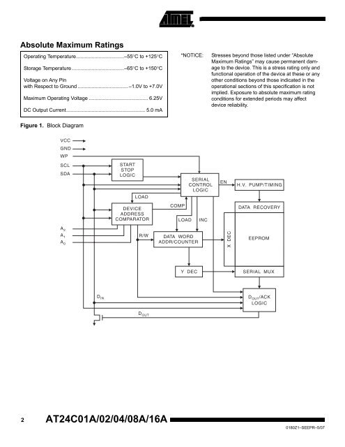
Absolute Maximum Ratings Operating Temperature..................................–55°C to +125°C *NOTICE: Stresses beyond those listed under “Absolute Storage Temperature .....................................–65°C to +150°C Voltage on Any Pin with Respect to Ground ....................................–1.0V to +7.0V Maximum Operating Voltage .......................................... 6.25V DC Output Current........................................................ 5.0 mA Figure 1. Block Diagram 2 AT24C01A/02/04/08A/16A Maximum Ratings” may cause permanent damage to the device. This is a stress rating only and functional operation of the device at these or any other conditions beyond those indicated in the operational sections of this specification is not implied. Exposure to absolute maximum rating conditions for extended periods may affect device reliability. 0180Z1–SEEPR–5/07
0180Z1–SEEPR–5/07 AT24C01A/02/04/08A/16A Pin Description SERIAL CLOCK (SCL): The SCL input is used to positive edge clock data into each EEPROM device and negative edge clock data out of each device. SERIAL DATA (SDA): The SDA pin is bidirectional for serial data transfer. This pin is open-drain driven and may be wire-ORed with any number of other open-drain or opencollector devices. DEVICE/PAGE ADDRESSES (A2, A1, A0): The A2, A1 and A0 pins are device address inputs that are hard wired for the AT24C01A and the AT24C02. As many as eight 1K/2K devices may be addressed on a single bus system (device addressing is discussed in detail under the Device Addressing section). The AT24C04 uses the A2 and A1 inputs for hard wire addressing and a total of four 4K devices may be addressed on a single bus system. The A0 pin is a no connect and can be connected to ground. The AT24C08A only uses the A2 input for hardwire addressing and a total of two 8K devices may be addressed on a single bus system. The A0 and A1 pins are no connects and can be connected to ground. The AT24C16A does not use the device address pins, which limits the number of devices on a single bus to one. The A0, A1 and A2 pins are no connects and can be connected to ground. WRITE PROTECT (WP): The AT24C01A/02/04/08A/16A has a Write Protect pin that provides hardware data protection. The Write Protect pin allows normal Read/Write operations when connected to ground (GND). When the Write Protect pin is connected to VCC, the write protection feature is enabled and operates as shown in Table 2. Table 2. Write Protect WP Pin Status At V CC Part of the Array Protected 24C01A 24C02 24C04 24C08A 24C16A Full (1K) Array Full (2K) Array At GND Normal Read/Write Operations Full (4K) Array Full (8K) Array Full (16K) Array Memory Organization AT24C01A, 1K SERIAL EEPROM: Internally organized with 16 pages of 8 bytes each, the 1K requires a 7-bit data word address for random word addressing. AT24C02, 2K SERIAL EEPROM: Internally organized with 32 pages of 8 bytes each, the 2K requires an 8-bit data word address for random word addressing. AT24C04, 4K SERIAL EEPROM: Internally organized with 32 pages of 16 bytes each, the 4K requires a 9-bit data word address for random word addressing. AT24C08A, 8K SERIAL EEPROM: Internally organized with 64 pages of 16 bytes each, the 8K requires a 10-bit data word address for random word addressing. AT24C16A, 16K SERIAL EEPROM: Internally organized with 128 pages of 16 bytes each, the 16K requires an 11-bit data word address for random word addressing. 3
- Page 1: Features • Low-voltage and Standa
- Page 5 and 6: Note: 1. This parameter is characte
- Page 7 and 8: Bus Timing Figure 2. SCL: Serial Cl
- Page 9 and 10: 0180Z1-SEEPR-5/07 AT24C01A/02/04/08
- Page 11 and 12: Figure 7. Device Address Figure 8.
- Page 13 and 14: AT24C01A Ordering Information (1) 0
- Page 15 and 16: AT24C04 Ordering Information (1) 01
- Page 17 and 18: AT24C16A Ordering Information (1) 0
- Page 19 and 20: 8S1 - JEDEC SOIC Note: 0180Z1-SEEPR
- Page 21 and 22: 8Y1 - MAP 0180Z1-SEEPR-5/07 R D PIN
- Page 23 and 24: 5TS1 - SOT23 0180Z1-SEEPR-5/07 R Se
- Page 25 and 26: 8U3-1 - dBGA2 (d1) (e1) 0180Z1-SEEP
- Page 27: Atmel Corporation Atmel Operations
Absolute Maximum Ratings<br />
Operating Temperature..................................–55°C to +125°C *NOTICE: Stresses beyond those listed under “Absolute<br />
Storage Temperature .....................................–65°C to +150°C<br />
Voltage on Any Pin<br />
with Respect to Ground ....................................–1.0V to +7.0V<br />
Maximum Operating Voltage .......................................... 6.25V<br />
DC Output Current........................................................ 5.0 mA<br />
Figure 1. Block Diagram<br />
2 <strong>AT24C01A</strong>/02/04/08A/16A<br />
Maximum Ratings” may cause permanent damage<br />
to the device. This is a stress rating only and<br />
functional operation of the device at these or any<br />
other conditions beyond those indicated in the<br />
operational sections of this specification is not<br />
implied. Exposure to absolute maximum rating<br />
conditions for extended periods may affect<br />
device reliability.<br />
0180Z1–SEEPR–5/07


