

ATmega128/L Datasheet Summary - Atmel Corporation
ATmega128/L Datasheet Summary - Atmel Corporation
ATmega128/L Datasheet Summary - Atmel Corporation

Create successful ePaper yourself
Turn your PDF publications into a flip-book with our unique Google optimized e-Paper software.
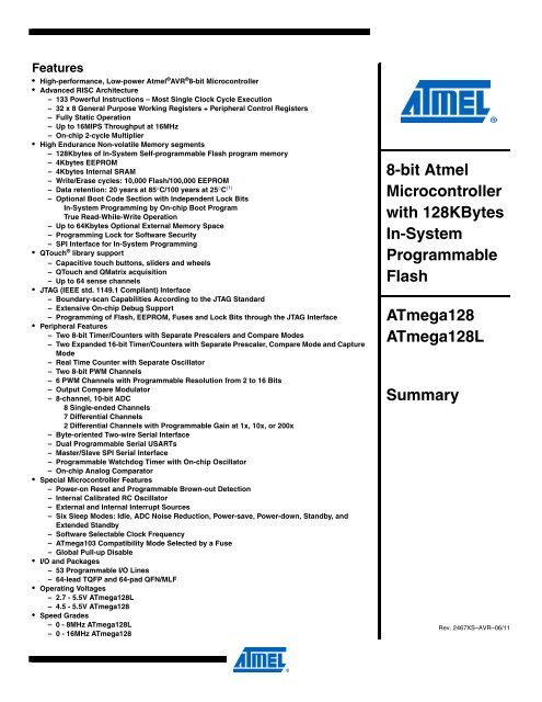
Features<br />
• High-performance, Low-power <strong>Atmel</strong> ® AVR ® 8-bit Microcontroller<br />
Advanced RISC Architecture<br />
– 133 Powerful Instructions – Most Single Clock Cycle Execution<br />
– 32 x 8 General Purpose Working Registers + Peripheral Control Registers<br />
– Fully Static Operation<br />
– Up to 16MIPS Throughput at 16MHz<br />
– On-chip 2-cycle Multiplier<br />
High Endurance Non-volatile Memory segments<br />
– 128Kbytes of In-System Self-programmable Flash program memory<br />
– 4Kbytes EEPROM<br />
– 4Kbytes Internal SRAM<br />
– Write/Erase cycles: 10,000 Flash/100,000 EEPROM<br />
– Data retention: 20 years at 85°C/100 years at 25°C (1)<br />
– Optional Boot Code Section with Independent Lock Bits<br />
In-System Programming by On-chip Boot Program<br />
True Read-While-Write Operation<br />
– Up to 64Kbytes Optional External Memory Space<br />
– Programming Lock for Software Security<br />
– SPI Interface for In-System Programming<br />
QTouch ® library support<br />
– Capacitive touch buttons, sliders and wheels<br />
– QTouch and QMatrix acquisition<br />
– Up to 64 sense channels<br />
JTAG (IEEE std. 1149.1 Compliant) Interface<br />
– Boundary-scan Capabilities According to the JTAG Standard<br />
– Extensive On-chip Debug Support<br />
– Programming of Flash, EEPROM, Fuses and Lock Bits through the JTAG Interface<br />
Peripheral Features<br />
– Two 8-bit Timer/Counters with Separate Prescalers and Compare Modes<br />
– Two Expanded 16-bit Timer/Counters with Separate Prescaler, Compare Mode and Capture<br />
Mode<br />
– Real Time Counter with Separate Oscillator<br />
– Two 8-bit PWM Channels<br />
– 6 PWM Channels with Programmable Resolution from 2 to 16 Bits<br />
– Output Compare Modulator<br />
– 8-channel, 10-bit ADC<br />
8 Single-ended Channels<br />
7 Differential Channels<br />
2 Differential Channels with Programmable Gain at 1x, 10x, or 200x<br />
– Byte-oriented Two-wire Serial Interface<br />
– Dual Programmable Serial USARTs<br />
– Master/Slave SPI Serial Interface<br />
– Programmable Watchdog Timer with On-chip Oscillator<br />
– On-chip Analog Comparator<br />
Special Microcontroller Features<br />
– Power-on Reset and Programmable Brown-out Detection<br />
– Internal Calibrated RC Oscillator<br />
– External and Internal Interrupt Sources<br />
– Six Sleep Modes: Idle, ADC Noise Reduction, Power-save, Power-down, Standby, and<br />
Extended Standby<br />
– Software Selectable Clock Frequency<br />
– ATmega103 Compatibility Mode Selected by a Fuse<br />
– Global Pull-up Disable<br />
I/O and Packages<br />
– 53 Programmable I/O Lines<br />
– 64-lead TQFP and 64-pad QFN/MLF<br />
Operating Voltages<br />
– 2.7 - 5.5V <strong>ATmega128</strong>L<br />
– 4.5 - 5.5V <strong>ATmega128</strong><br />
Speed Grades<br />
– 0 - 8MHz <strong>ATmega128</strong>L<br />
– 0 - 16MHz <strong>ATmega128</strong><br />
8-bit <strong>Atmel</strong><br />
Microcontroller<br />
with 128KBytes<br />
In-System<br />
Programmable<br />
Flash<br />
<strong>ATmega128</strong><br />
<strong>ATmega128</strong>L<br />
<strong>Summary</strong><br />
Rev. 2467XS–AVR–06/11
Pin<br />
Configurations<br />
Figure 1. Pinout <strong>ATmega128</strong><br />
2467XS–AVR–06/11<br />
PEN<br />
RXD0/(PDI) PE0<br />
(TXD0/PDO) PE1<br />
(XCK0/AIN0) PE2<br />
(OC3A/AIN1) PE3<br />
(OC3B/INT4) PE4<br />
(OC3C/INT5) PE5<br />
(T3/INT6) PE6<br />
(ICP3/INT7) PE7<br />
(SS) PB0<br />
(SCK) PB1<br />
(MOSI) PB2<br />
(MISO) PB3<br />
(OC0) PB4<br />
(OC1A) PB5<br />
(OC1B) PB6<br />
1<br />
2<br />
3<br />
4<br />
5<br />
6<br />
7<br />
8<br />
9<br />
10<br />
11<br />
12<br />
13<br />
14<br />
15<br />
16<br />
AVCC<br />
GND<br />
AREF<br />
PF0 (ADC0)<br />
PF1 (ADC1)<br />
PF2 (ADC2)<br />
PF3 (ADC3)<br />
PF4 (ADC4/TCK)<br />
PF5 (ADC5/TMS)<br />
PF6 (ADC6/TDO)<br />
PF7 (ADC7/TDI)<br />
GND<br />
VCC<br />
PA0 (AD0)<br />
PA1 (AD1)<br />
PA2 (AD2)<br />
64<br />
63<br />
62<br />
61<br />
60<br />
59<br />
58<br />
57<br />
56<br />
55<br />
54<br />
53<br />
52<br />
51<br />
50<br />
17<br />
18<br />
19<br />
20<br />
21<br />
22<br />
23<br />
24<br />
25<br />
26<br />
27<br />
28<br />
29<br />
30<br />
31<br />
<strong>ATmega128</strong><br />
Note: The Pinout figure applies to both TQFP and MLF packages. The bottom pad under the QFN/MLF<br />
package should be soldered to ground.<br />
Overview The <strong>Atmel</strong> ® AVR ® <strong>ATmega128</strong> is a low-power CMOS 8-bit microcontroller based on the AVR<br />
enhanced RISC architecture. By executing powerful instructions in a single clock cycle, the<br />
<strong>ATmega128</strong> achieves throughputs approaching 1MIPS per MHz allowing the system designer to<br />
optimize power consumption versus processing speed.<br />
49<br />
32<br />
(OC2/OC1C) PB7<br />
TOSC2/PG3<br />
TOSC1/PG4<br />
RESET<br />
VCC<br />
GND<br />
XTAL2<br />
XTAL1<br />
(SCL/INT0) PD0<br />
(SDA/INT1) PD1<br />
(RXD1/INT2) PD2<br />
(TXD1/INT3) PD3<br />
(ICP1) PD4<br />
(XCK1) PD5<br />
(T1) PD6<br />
(T2) PD7<br />
48<br />
47<br />
46<br />
45<br />
44<br />
43<br />
42<br />
41<br />
40<br />
39<br />
38<br />
37<br />
36<br />
35<br />
34<br />
33<br />
PA3 (AD3)<br />
PA4 (AD4)<br />
PA5 (AD5)<br />
PA6 (AD6)<br />
PA7 (AD7)<br />
PG2(ALE)<br />
PC7 (A15)<br />
PC6 (A14)<br />
PC5 (A13)<br />
PC4 (A12)<br />
PC3 (A11)<br />
PC2 (A10)<br />
PC1 (A9)<br />
PC0 (A8)<br />
PG1(RD)<br />
PG0(WR)<br />
2
Block Diagram<br />
Figure 2. Block Diagram<br />
VCC<br />
GND<br />
AVCC<br />
AGND<br />
AREF<br />
PEN<br />
ANALOG<br />
COMPARATOR<br />
2467XS–AVR–06/11<br />
JTAG TAP<br />
ON-CHIP DEBUG<br />
BOUNDARY-<br />
SCAN<br />
PROGRAMMING<br />
LOGIC<br />
+<br />
-<br />
DATA REGISTER<br />
PORTF<br />
USART0<br />
DATA REGISTER<br />
PORTE<br />
PF0 - PF7<br />
PORTF DRIVERS<br />
PROGRAM<br />
COUNTER<br />
PROGRAM<br />
FLASH<br />
INSTRUCTION<br />
REGISTER<br />
INSTRUCTION<br />
DECODER<br />
PORTE DRIVERS<br />
PE0 - PE7<br />
DATA DIR.<br />
REG. PORTF<br />
ADC<br />
CONTROL<br />
LINES<br />
DATA DIR.<br />
REG. PORTE<br />
DATA REGISTER<br />
PORTA<br />
STACK<br />
POINTER<br />
SRAM<br />
GENERAL<br />
PURPOSE<br />
REGISTERS<br />
X<br />
Y<br />
Z<br />
ALU<br />
STATUS<br />
REGISTER<br />
DATA REGISTER<br />
PORTB<br />
PORTA DRIVERS<br />
PORTB DRIVERS<br />
PB0 - PB7<br />
PA0 - PA7<br />
DATA DIR.<br />
REG. PORTA<br />
DATA DIR.<br />
REG. PORTB<br />
INTERNAL<br />
OSCILLATOR<br />
WATCHDOG<br />
TIMER<br />
MCU CONTROL<br />
REGISTER<br />
TIMER/<br />
COUNTERS<br />
INTERRUPT<br />
UNIT<br />
EEPROM<br />
SPI<br />
8-BIT DATA BUS<br />
DATA REGISTER<br />
PORTD<br />
DATA REGISTER<br />
PORTC<br />
OSCILLATOR<br />
OSCILLATOR<br />
TIMING AND<br />
CONTROL<br />
PORTD DRIVERS<br />
PC0 - PC7<br />
PORTC DRIVERS<br />
CALIB. OSC<br />
PD0 - PD7<br />
USART1<br />
DATA DIR.<br />
REG. PORTD<br />
DATA DIR.<br />
REG. PORTC<br />
<strong>ATmega128</strong><br />
XTAL1<br />
TWO-WIRE SERIAL<br />
INTERFACE<br />
DATA REG.<br />
PORTG<br />
XTAL2<br />
RESET<br />
DATA DIR.<br />
REG. PORTG<br />
PORTG DRIVERS<br />
PG0 - PG4<br />
3
ATmega103 and<br />
<strong>ATmega128</strong><br />
Compatibility<br />
2467XS–AVR–06/11<br />
<strong>ATmega128</strong><br />
The <strong>Atmel</strong> ® AVR ® core combines a rich instruction set with 32 general purpose working registers.<br />
All the 32 registers are directly connected to the Arithmetic Logic Unit (ALU), allowing two<br />
independent registers to be accessed in one single instruction executed in one clock cycle. The<br />
resulting architecture is more code efficient while achieving throughputs up to ten times faster<br />
than conventional CISC microcontrollers.<br />
The <strong>ATmega128</strong> provides the following features: 128Kbytes of In-System Programmable Flash<br />
with Read-While-Write capabilities, 4Kbytes EEPROM, 4Kbytes SRAM, 53 general purpose I/O<br />
lines, 32 general purpose working registers, Real Time Counter (RTC), four flexible Timer/Counters<br />
with compare modes and PWM, 2 USARTs, a byte oriented Two-wire Serial Interface, an 8channel,<br />
10-bit ADC with optional differential input stage with programmable gain, programmable<br />
Watchdog Timer with Internal Oscillator, an SPI serial port, IEEE std. 1149.1 compliant<br />
JTAG test interface, also used for accessing the On-chip Debug system and programming and<br />
six software selectable power saving modes. The Idle mode stops the CPU while allowing the<br />
SRAM, Timer/Counters, SPI port, and interrupt system to continue functioning. The Power-down<br />
mode saves the register contents but freezes the Oscillator, disabling all other chip functions<br />
until the next interrupt or Hardware Reset. In Power-save mode, the asynchronous timer continues<br />
to run, allowing the user to maintain a timer base while the rest of the device is sleeping.<br />
The ADC Noise Reduction mode stops the CPU and all I/O modules except Asynchronous<br />
Timer and ADC, to minimize switching noise during ADC conversions. In Standby mode, the<br />
Crystal/Resonator Oscillator is running while the rest of the device is sleeping. This allows very<br />
fast start-up combined with low power consumption. In Extended Standby mode, both the main<br />
Oscillator and the Asynchronous Timer continue to run.<br />
<strong>Atmel</strong> offers the QTouch ® library for embedding capacitive touch buttons, sliders and wheels<br />
functionality into AVR microcontrollers. The patented charge-transfer signal acquisition offers<br />
robust sensing and includes fully debounced reporting of touch keys and includes Adjacent Key<br />
Suppression ® (AKS) technology for unambiguous detection of key events. The easy-to-use<br />
QTouch Suite toolchain allows you to explore, develop and debug your own touch applications.<br />
The device is manufactured using <strong>Atmel</strong>’s high-density nonvolatile memory technology. The Onchip<br />
ISP Flash allows the program memory to be reprogrammed in-system through an SPI serial<br />
interface, by a conventional nonvolatile memory programmer, or by an On-chip Boot program<br />
running on the AVR core. The boot program can use any interface to download the application<br />
program in the application Flash memory. Software in the Boot Flash section will continue to run<br />
while the Application Flash section is updated, providing true Read-While-Write operation. By<br />
combining an 8-bit RISC CPU with In-System Self-Programmable Flash on a monolithic chip,<br />
the <strong>Atmel</strong> <strong>ATmega128</strong> is a powerful microcontroller that provides a highly flexible and cost effective<br />
solution to many embedded control applications.<br />
The <strong>ATmega128</strong> device is supported with a full suite of program and system development tools<br />
including: C compilers, macro assemblers, program debugger/simulators, in-circuit emulators,<br />
and evaluation kits.<br />
The <strong>ATmega128</strong> is a highly complex microcontroller where the number of I/O locations supersedes<br />
the 64 I/O locations reserved in the AVR instruction set. To ensure backward compatibility<br />
with the ATmega103, all I/O locations present in ATmega103 have the same location in<br />
<strong>ATmega128</strong>. Most additional I/O locations are added in an Extended I/O space starting from $60<br />
to $FF, (i.e., in the ATmega103 internal RAM space). These locations can be reached by using<br />
LD/LDS/LDD and ST/STS/STD instructions only, not by using IN and OUT instructions. The relocation<br />
of the internal RAM space may still be a problem for ATmega103 users. Also, the<br />
increased number of interrupt vectors might be a problem if the code uses absolute addresses.<br />
To solve these problems, an ATmega103 compatibility mode can be selected by programming<br />
the fuse M103C. In this mode, none of the functions in the Extended I/O space are in use, so the<br />
internal RAM is located as in ATmega103. Also, the Extended Interrupt vectors are removed.<br />
4
ATmega103<br />
Compatibility Mode<br />
Pin Descriptions<br />
VCC Digital supply voltage.<br />
GND Ground.<br />
2467XS–AVR–06/11<br />
<strong>ATmega128</strong><br />
The <strong>ATmega128</strong> is 100% pin compatible with ATmega103, and can replace the ATmega103 on<br />
current Printed Circuit Boards. The application note “Replacing ATmega103 by <strong>ATmega128</strong>”<br />
describes what the user should be aware of replacing the ATmega103 by an <strong>ATmega128</strong>.<br />
By programming the M103C fuse, the <strong>Atmel</strong> ® <strong>ATmega128</strong> will be compatible with the<br />
ATmega103 regards to RAM, I/O pins and interrupt vectors as described above. However, some<br />
new features in <strong>ATmega128</strong> are not available in this compatibility mode, these features are<br />
listed below:<br />
One USART instead of two, Asynchronous mode only. Only the eight least significant bits of<br />
the Baud Rate Register is available.<br />
One 16 bits Timer/Counter with two compare registers instead of two 16-bit Timer/Counters<br />
with three compare registers.<br />
Two-wire serial interface is not supported.<br />
Port C is output only.<br />
Port G serves alternate functions only (not a general I/O port).<br />
Port F serves as digital input only in addition to analog input to the ADC.<br />
Boot Loader capabilities is not supported.<br />
It is not possible to adjust the frequency of the internal calibrated RC Oscillator.<br />
The External Memory Interface can not release any Address pins for general I/O, neither<br />
configure different wait-states to different External Memory Address sections.<br />
In addition, there are some other minor differences to make it more compatible to ATmega103:<br />
Only EXTRF and PORF exists in MCUCSR.<br />
Timed sequence not required for Watchdog Time-out change.<br />
External Interrupt pins 3 - 0 serve as level interrupt only.<br />
USART has no FIFO buffer, so data overrun comes earlier.<br />
Unused I/O bits in ATmega103 should be written to 0 to ensure same operation in <strong>ATmega128</strong>.<br />
Port A (PA7..PA0) Port A is an 8-bit bi-directional I/O port with internal pull-up resistors (selected for each bit). The<br />
Port A output buffers have symmetrical drive characteristics with both high sink and source<br />
capability. As inputs, Port A pins that are externally pulled low will source current if the pull-up<br />
resistors are activated. The Port A pins are tri-stated when a reset condition becomes active,<br />
even if the clock is not running.<br />
Port A also serves the functions of various special features of the <strong>ATmega128</strong> as listed on page<br />
72.<br />
Port B (PB7..PB0) Port B is an 8-bit bi-directional I/O port with internal pull-up resistors (selected for each bit). The<br />
Port B output buffers have symmetrical drive characteristics with both high sink and source<br />
capability. As inputs, Port B pins that are externally pulled low will source current if the pull-up<br />
resistors are activated. The Port B pins are tri-stated when a reset condition becomes active,<br />
even if the clock is not running.<br />
Port B also serves the functions of various special features of the <strong>ATmega128</strong> as listed on page<br />
73.<br />
5
2467XS–AVR–06/11<br />
<strong>ATmega128</strong><br />
Port C (PC7..PC0) Port C is an 8-bit bi-directional I/O port with internal pull-up resistors (selected for each bit). The<br />
Port C output buffers have symmetrical drive characteristics with both high sink and source<br />
capability. As inputs, Port C pins that are externally pulled low will source current if the pull-up<br />
resistors are activated. The Port C pins are tri-stated when a reset condition becomes active,<br />
even if the clock is not running.<br />
Port C also serves the functions of special features of the <strong>Atmel</strong> ® AVR ® <strong>ATmega128</strong> as listed on<br />
page 76. In ATmega103 compatibility mode, Port C is output only, and the port C pins are not tristated<br />
when a reset condition becomes active.<br />
Note: The <strong>ATmega128</strong> is by default shipped in ATmega103 compatibility mode. Thus, if the parts are not<br />
programmed before they are put on the PCB, PORTC will be output during first power up, and until<br />
the ATmega103 compatibility mode is disabled.<br />
Port D (PD7..PD0) Port D is an 8-bit bi-directional I/O port with internal pull-up resistors (selected for each bit). The<br />
Port D output buffers have symmetrical drive characteristics with both high sink and source<br />
capability. As inputs, Port D pins that are externally pulled low will source current if the pull-up<br />
resistors are activated. The Port D pins are tri-stated when a reset condition becomes active,<br />
even if the clock is not running.<br />
Port D also serves the functions of various special features of the <strong>ATmega128</strong> as listed on page<br />
77.<br />
Port E (PE7..PE0) Port E is an 8-bit bi-directional I/O port with internal pull-up resistors (selected for each bit). The<br />
Port E output buffers have symmetrical drive characteristics with both high sink and source<br />
capability. As inputs, Port E pins that are externally pulled low will source current if the pull-up<br />
resistors are activated. The Port E pins are tri-stated when a reset condition becomes active,<br />
even if the clock is not running.<br />
Port E also serves the functions of various special features of the <strong>ATmega128</strong> as listed on page<br />
80.<br />
Port F (PF7..PF0) Port F serves as the analog inputs to the A/D Converter.<br />
Port F also serves as an 8-bit bi-directional I/O port, if the A/D Converter is not used. Port pins<br />
can provide internal pull-up resistors (selected for each bit). The Port F output buffers have symmetrical<br />
drive characteristics with both high sink and source capability. As inputs, Port F pins<br />
that are externally pulled low will source current if the pull-up resistors are activated. The Port F<br />
pins are tri-stated when a reset condition becomes active, even if the clock is not running. If the<br />
JTAG interface is enabled, the pull-up resistors on pins PF7(TDI), PF5(TMS), and PF4(TCK) will<br />
be activated even if a Reset occurs.<br />
The TDO pin is tri-stated unless TAP states that shift out data are entered.<br />
Port F also serves the functions of the JTAG interface.<br />
In ATmega103 compatibility mode, Port F is an input Port only.<br />
Port G (PG4..PG0) Port G is a 5-bit bi-directional I/O port with internal pull-up resistors (selected for each bit). The<br />
Port G output buffers have symmetrical drive characteristics with both high sink and source<br />
capability. As inputs, Port G pins that are externally pulled low will source current if the pull-up<br />
resistors are activated. The Port G pins are tri-stated when a reset condition becomes active,<br />
even if the clock is not running.<br />
Port G also serves the functions of various special features.<br />
The port G pins are tri-stated when a reset condition becomes active, even if the clock is not<br />
running.<br />
6
2467XS–AVR–06/11<br />
<strong>ATmega128</strong><br />
In ATmega103 compatibility mode, these pins only serves as strobes signals to the external<br />
memory as well as input to the 32kHz Oscillator, and the pins are initialized to PG0 = 1, PG1 = 1,<br />
and PG2 = 0 asynchronously when a reset condition becomes active, even if the clock is not<br />
running. PG3 and PG4 are oscillator pins.<br />
RESET Reset input. A low level on this pin for longer than the minimum pulse length will generate a<br />
reset, even if the clock is not running. The minimum pulse length is given in Table 19 on page<br />
50. Shorter pulses are not guaranteed to generate a reset.<br />
XTAL1 Input to the inverting Oscillator amplifier and input to the internal clock operating circuit.<br />
XTAL2 Output from the inverting Oscillator amplifier.<br />
AVCC AVCC is the supply voltage pin for Port F and the A/D Converter. It should be externally connected<br />
to V CC , even if the ADC is not used. If the ADC is used, it should be connected to V CC<br />
through a low-pass filter.<br />
AREF AREF is the analog reference pin for the A/D Converter.<br />
PEN PEN is a programming enable pin for the SPI Serial Programming mode, and is internally pulled<br />
high . By holding this pin low during a Power-on Reset, the device will enter the SPI Serial Programming<br />
mode. PEN has no function during normal operation.<br />
7
2467XS–AVR–06/11<br />
<strong>ATmega128</strong><br />
Resources A comprehensive set of development tools, application notes, and datasheets are available for<br />
download on http://www.atmel.com/avr.<br />
Note: 1.<br />
Data Retention Reliability Qualification results show that the projected data retention failure rate is much less<br />
than 1 PPM over 20 years at 85°C or 100 years at 25°C<br />
About Code<br />
Examples<br />
Capacitive touch sensing<br />
This datasheet contains simple code examples that briefly show how to use various parts of the<br />
device. These code examples assume that the part specific header file is included before compilation.<br />
Be aware that not all C compiler vendors include bit definitions in the header files and<br />
interrupt handling in C is compiler dependent. Please confirm with the C compiler documentation<br />
for more details.<br />
For I/O registers located in extended I/O map, “IN”, “OUT”, “SBIS”, “SBIC”, “CBI”, and “SBI”<br />
instructions must be replaced with instructions that allow access to extended I/O. Typically<br />
“LDS” and “STS” combined with “SBRS”, “SBRC”, “SBR”, and “CBR”.<br />
The <strong>Atmel</strong> QTouch Library provides a simple to use solution to realize touch sensitive interfaces<br />
on most <strong>Atmel</strong> AVR microcontrollers. The QTouch Library includes support for the QTouch and<br />
QMatrix acquisition methods.<br />
Touch sensing can be added to any application by linking the appropriate <strong>Atmel</strong> QTouch Library<br />
for the AVR Microcontroller. This is done by using a simple set of APIs to define the touch channels<br />
and sensors, and then calling the touch sensing API’s to retrieve the channel information<br />
and determine the touch sensor states.<br />
The QTouch Library is FREE and downloadable from the <strong>Atmel</strong> website at the following location:<br />
www.atmel.com/qtouchlibrary. For implementation details and other information, refer to the<br />
<strong>Atmel</strong> QTouch Library User Guide - also available for download from the <strong>Atmel</strong> website.<br />
8
Instruction Set <strong>Summary</strong><br />
2467XS–AVR–06/11<br />
<strong>ATmega128</strong><br />
Mnemonics Operands Description Operation Flags #Clocks<br />
ARITHMETIC AND LOGIC INSTRUCTIONS<br />
ADD Rd, Rr Add two Registers Rd ← Rd + Rr Z,C,N,V,H 1<br />
ADC Rd, Rr Add with Carry two Registers Rd ← Rd + Rr + C Z,C,N,V,H 1<br />
ADIW Rdl,K Add Immediate to Word Rdh:Rdl ← Rdh:Rdl + K Z,C,N,V,S 2<br />
SUB Rd, Rr Subtract two Registers Rd ← Rd - Rr Z,C,N,V,H 1<br />
SUBI Rd, K Subtract Constant from Register Rd ← Rd - K Z,C,N,V,H 1<br />
SBC Rd, Rr Subtract with Carry two Registers Rd ← Rd - Rr - C Z,C,N,V,H 1<br />
SBCI Rd, K Subtract with Carry Constant from Reg. Rd ← Rd - K - C Z,C,N,V,H 1<br />
SBIW Rdl,K Subtract Immediate from Word Rdh:Rdl ← Rdh:Rdl - K Z,C,N,V,S 2<br />
AND Rd, Rr Logical AND Registers Rd ← Rd • Rr Z,N,V 1<br />
ANDI Rd, K Logical AND Register and Constant Rd ← Rd • K Z,N,V 1<br />
OR Rd, Rr Logical OR Registers Rd ← Rd v Rr Z,N,V 1<br />
ORI Rd, K Logical OR Register and Constant Rd ← Rd v K Z,N,V 1<br />
EOR Rd, Rr Exclusive OR Registers Rd ← Rd ⊕ Rr Z,N,V 1<br />
COM Rd One’s Complement Rd ← $FF − Rd Z,C,N,V 1<br />
NEG Rd Two’s Complement Rd ← $00 − Rd Z,C,N,V,H 1<br />
SBR Rd,K Set Bit(s) in Register Rd ← Rd v K Z,N,V 1<br />
CBR Rd,K Clear Bit(s) in Register Rd ← Rd • ($FF - K) Z,N,V 1<br />
INC Rd Increment Rd ← Rd + 1 Z,N,V 1<br />
DEC Rd Decrement Rd ← Rd − 1 Z,N,V 1<br />
TST Rd Test for Zero or Minus Rd ← Rd • Rd Z,N,V 1<br />
CLR Rd Clear Register Rd ← Rd ⊕ Rd Z,N,V 1<br />
SER Rd Set Register Rd ← $FF None 1<br />
MUL Rd, Rr Multiply Unsigned R1:R0 ← Rd x Rr Z,C 2<br />
MULS Rd, Rr Multiply Signed R1:R0 ← Rd x Rr Z,C 2<br />
MULSU Rd, Rr Multiply Signed with Unsigned R1:R0 ← Rd x Rr Z,C 2<br />
FMUL Rd, Rr Fractional Multiply Unsigned R1:R0 ← (Rd x Rr)
Instruction Set <strong>Summary</strong> (Continued)<br />
2467XS–AVR–06/11<br />
<strong>ATmega128</strong><br />
Mnemonics Operands Description Operation Flags #Clocks<br />
BRIE k Branch if Interrupt Enabled if ( I = 1) then PC ← PC + k + 1 None 1 / 2<br />
BRID k Branch if Interrupt Disabled if ( I = 0) then PC ← PC + k + 1 None 1 / 2<br />
DATA TRANSFER INSTRUCTIONS<br />
MOV Rd, Rr Move Between Registers Rd ← Rr None 1<br />
MOVW Rd, Rr Copy Register Word Rd+1:Rd ← Rr+1:Rr None 1<br />
LDI Rd, K Load Immediate Rd ← K None 1<br />
LD Rd, X Load Indirect Rd ← (X) None 2<br />
LD Rd, X+ Load Indirect and Post-Inc. Rd ← (X), X ← X + 1 None 2<br />
LD Rd, - X Load Indirect and Pre-Dec. X ← X - 1, Rd ← (X) None 2<br />
LD Rd, Y Load Indirect Rd ← (Y) None 2<br />
LD Rd, Y+ Load Indirect and Post-Inc. Rd ← (Y), Y ← Y + 1 None 2<br />
LD Rd, - Y Load Indirect and Pre-Dec. Y ← Y - 1, Rd ← (Y) None 2<br />
LDD Rd,Y+q Load Indirect with Displacement Rd ← (Y + q) None 2<br />
LD Rd, Z Load Indirect Rd ← (Z) None 2<br />
LD Rd, Z+ Load Indirect and Post-Inc. Rd ← (Z), Z ← Z+1 None 2<br />
LD Rd, -Z Load Indirect and Pre-Dec. Z ← Z - 1, Rd ← (Z) None 2<br />
LDD Rd, Z+q Load Indirect with Displacement Rd ← (Z + q) None 2<br />
LDS Rd, k Load Direct from SRAM Rd ← (k) None 2<br />
ST X, Rr Store Indirect (X) ← Rr None 2<br />
ST X+, Rr Store Indirect and Post-Inc. (X) ← Rr, X ← X + 1 None 2<br />
ST - X, Rr Store Indirect and Pre-Dec. X ← X - 1, (X) ← Rr None 2<br />
ST Y, Rr Store Indirect (Y) ← Rr None 2<br />
ST Y+, Rr Store Indirect and Post-Inc. (Y) ← Rr, Y ← Y + 1 None 2<br />
ST - Y, Rr Store Indirect and Pre-Dec. Y ← Y - 1, (Y) ← Rr None 2<br />
STD Y+q,Rr Store Indirect with Displacement (Y + q) ← Rr None 2<br />
ST Z, Rr Store Indirect (Z) ← Rr None 2<br />
ST Z+, Rr Store Indirect and Post-Inc. (Z) ← Rr, Z ← Z + 1 None 2<br />
ST -Z, Rr Store Indirect and Pre-Dec. Z ← Z - 1, (Z) ← Rr None 2<br />
STD Z+q,Rr Store Indirect with Displacement (Z + q) ← Rr None 2<br />
STS k, Rr Store Direct to SRAM (k) ← Rr None 2<br />
LPM Load Program Memory R0 ← (Z) None 3<br />
LPM Rd, Z Load Program Memory Rd ← (Z) None 3<br />
LPM Rd, Z+ Load Program Memory and Post-Inc Rd ← (Z), Z ← Z+1 None 3<br />
ELPM Extended Load Program Memory R0 ← (RAMPZ:Z) None 3<br />
ELPM Rd, Z Extended Load Program Memory Rd ← (RAMPZ:Z) None 3<br />
ELPM Rd, Z+ Extended Load Program Memory and Post-Inc Rd ← (RAMPZ:Z), RAMPZ:Z ← RAMPZ:Z+1 None 3<br />
SPM Store Program Memory (Z) ← R1:R0 None -<br />
IN Rd, P In Port Rd ← P None 1<br />
OUT P, Rr Out Port P ← Rr None 1<br />
PUSH Rr Push Register on Stack STACK ← Rr None 2<br />
POP Rd Pop Register from Stack Rd ← STACK None 2<br />
BIT AND BIT-TEST INSTRUCTIONS<br />
SBI P,b Set Bit in I/O Register I/O(P,b) ← 1 None 2<br />
CBI P,b Clear Bit in I/O Register I/O(P,b) ← 0 None 2<br />
LSL Rd Logical Shift Left Rd(n+1) ← Rd(n), Rd(0) ← 0 Z,C,N,V 1<br />
LSR Rd Logical Shift Right Rd(n) ← Rd(n+1), Rd(7) ← 0 Z,C,N,V 1<br />
ROL Rd Rotate Left Through Carry Rd(0)←C,Rd(n+1)← Rd(n),C←Rd(7) Z,C,N,V 1<br />
ROR Rd Rotate Right Through Carry Rd(7)←C,Rd(n)← Rd(n+1),C←Rd(0) Z,C,N,V 1<br />
ASR Rd Arithmetic Shift Right Rd(n) ← Rd(n+1), n=0..6 Z,C,N,V 1<br />
SWAP Rd Swap Nibbles Rd(3..0)←Rd(7..4),Rd(7..4)←Rd(3..0) None 1<br />
BSET s Flag Set SREG(s) ← 1 SREG(s) 1<br />
BCLR s Flag Clear SREG(s) ← 0 SREG(s) 1<br />
BST Rr, b Bit Store from Register to T T ← Rr(b) T 1<br />
BLD Rd, b Bit load from T to Register Rd(b) ← T None 1<br />
SEC Set Carry C ← 1 C 1<br />
CLC Clear Carry C ← 0 C 1<br />
SEN Set Negative Flag N ← 1 N 1<br />
CLN Clear Negative Flag N ← 0 N 1<br />
SEZ Set Zero Flag Z ← 1 Z 1<br />
CLZ Clear Zero Flag Z ← 0 Z 1<br />
SEI Global Interrupt Enable I ← 1 I 1<br />
CLI Global Interrupt Disable I ← 0 I 1<br />
SES Set Signed Test Flag S ← 1 S 1<br />
CLS Clear Signed Test Flag S ← 0 S 1<br />
10
Instruction Set <strong>Summary</strong> (Continued)<br />
2467XS–AVR–06/11<br />
<strong>ATmega128</strong><br />
Mnemonics Operands Description Operation Flags #Clocks<br />
SEV Set Twos Complement Overflow. V ← 1 V 1<br />
CLV Clear Twos Complement Overflow V ← 0 V 1<br />
SET Set T in SREG T ← 1 T 1<br />
CLT Clear T in SREG T ← 0 T 1<br />
SEH Set Half Carry Flag in SREG H ← 1 H 1<br />
CLH<br />
MCU CONTROL INSTRUCTIONS<br />
Clear Half Carry Flag in SREG H ← 0 H 1<br />
NOP No Operation None 1<br />
SLEEP Sleep (see specific descr. for Sleep function) None 1<br />
WDR Watchdog Reset (see specific descr. for WDR/timer) None 1<br />
BREAK Break For On-chip Debug Only None N/A<br />
11
Ordering Information<br />
Speed (MHz) Power Supply Ordering Code (1)<br />
2467XS–AVR–06/11<br />
8 2.7 – 5.5V<br />
16 4.5 – 5.5V<br />
8 3.0 – 5.5V<br />
16 4.5 – 5.5V<br />
<strong>ATmega128</strong>L-8AU<br />
<strong>ATmega128</strong>L-8AUR (3)<br />
<strong>ATmega128</strong>L-8MU<br />
<strong>ATmega128</strong>L-8MUR (3)<br />
<strong>ATmega128</strong>-16AU<br />
<strong>ATmega128</strong>-16AUR (3)<br />
<strong>ATmega128</strong>-16MU<br />
<strong>ATmega128</strong>-16MUR (3)<br />
<strong>ATmega128</strong>L–8AN<br />
<strong>ATmega128</strong>L–8ANR (3)<br />
<strong>ATmega128</strong>L–8MN<br />
<strong>ATmega128</strong>L–8MNR (3)<br />
<strong>ATmega128</strong>–16AN<br />
<strong>ATmega128</strong>–16ANR (3)<br />
<strong>ATmega128</strong>–16MN<br />
<strong>ATmega128</strong>–16MNR (3)<br />
<strong>ATmega128</strong><br />
Package (2)<br />
Operation Range<br />
64A<br />
64A<br />
64M1<br />
64M1 Industrial<br />
(-40 o C to 85 o 64A<br />
C)<br />
64A<br />
64M1<br />
64M1<br />
64A<br />
64A<br />
64M1<br />
64M1 Extended<br />
64A<br />
(-40°C to 105°C)<br />
64A<br />
64M1<br />
64M1<br />
Notes: 1. Pb-free packaging complies to the European Directive for Restriction of Hazardous Substances (RoHS directive). Also<br />
Halide free and fully Green.<br />
2. The device can also be supplied in wafer form. Please contact your local <strong>Atmel</strong> sales office for detailed ordering information<br />
and minimum quantities.<br />
3. Tape and Reel<br />
Package Type<br />
64A 64-lead, 14 x 14 x 1.0mm, Thin Profile Plastic Quad Flat Package (TQFP)<br />
64M1 64-pad, 9 x 9 x 1.0mm, Quad Flat No-Lead/Micro Lead Frame Package (QFN/MLF)<br />
12
Packaging Information<br />
64A<br />
2467XS–AVR–06/11<br />
R<br />
C<br />
e<br />
PIN 1<br />
0°~7°<br />
2325 Orchard Parkway<br />
San Jose, CA 95131<br />
L<br />
PIN 1 IDENTIFIER<br />
D1<br />
D<br />
B<br />
E1 E<br />
Notes:<br />
1.This package conforms to JEDEC reference MS-026, Variation AEB.<br />
2. Dimensions D1 and E1 do not include mold protrusion. Allowable<br />
protrusion is 0.25 mm per side. Dimensions D1 and E1 are maximum<br />
plastic body size dimensions including mold mismatch.<br />
3. Lead coplanarity is 0.10 mm maximum.<br />
A1 A2 A<br />
COMMON DIMENSIONS<br />
(Unit of Measure = mm)<br />
<strong>ATmega128</strong><br />
SYMBOL MIN NOM MAX NOTE<br />
A – – 1.20<br />
A1 0.05 – 0.15<br />
A2 0.95 1.00 1.05<br />
D 15.75 16.00 16.25<br />
D1 13.90 14.00 14.10 Note 2<br />
E 15.75 16.00 16.25<br />
E1 13.90 14.00 14.10 Note 2<br />
B 0.30 – 0.45<br />
C 0.09 – 0.20<br />
L 0.45 – 0.75<br />
e 0.80 TYP<br />
TITLE DRAWING NO.<br />
64A, 64-lead, 14 x 14 mm Body Size, 1.0 mm Body Thickness,<br />
0.8 mm Lead Pitch, Thin Profile Plastic Quad Flat Package (TQFP)<br />
64A<br />
2010-10-20<br />
REV.<br />
C<br />
13
64M1<br />
K<br />
2467XS–AVR–06/11<br />
R<br />
L<br />
E2<br />
Notes:<br />
1. JEDEC Standard MO-220, (SAW Singulation) Fig. 1, VMMD.<br />
2. Dimension and tolerance conform to ASMEY14.5M-1994.<br />
2325 Orchard Parkway<br />
San Jose, CA 95131<br />
D<br />
Marked Pin# 1 ID<br />
K<br />
TOP VIEW<br />
D2<br />
b e<br />
BOTTOM VIEW<br />
1<br />
2<br />
3<br />
E<br />
Pin #1 Corner<br />
Option A<br />
Option B<br />
Option C<br />
Pin #1<br />
Triangle<br />
Pin #1<br />
Chamfer<br />
(C 0.30)<br />
Pin #1<br />
Notch<br />
(0.20 R)<br />
SIDE VIEW<br />
SEATING PLANE<br />
COMMON DIMENSIONS<br />
(Unit of Measure = mm)<br />
TITLE DRAWING NO.<br />
64M1, 64-pad, 9 x 9 x 1.0 mm Body, Lead Pitch 0.50 mm,<br />
5.40 mm Exposed Pad, Micro Lead Frame Package (MLF)<br />
64M1<br />
A<br />
C<br />
A1<br />
0.08<br />
<strong>ATmega128</strong><br />
SYMBOL MIN NOM MAX NOTE<br />
C<br />
A 0.80 0.90 1.00<br />
A1 – 0.02 0.05<br />
b 0.18 0.25 0.30<br />
D 8.90 9.00 9.10<br />
D2 5.20 5.40 5.60<br />
E 8.90 9.00 9.10<br />
E2 5.20 5.40 5.60<br />
e 0.50 BSC<br />
L 0.35 0.40 0.45<br />
K 1.25 1.40 1.55<br />
2010-10-19<br />
REV.<br />
H<br />
14
Errata The revision letter in this section refers to the revision of the <strong>ATmega128</strong> device.<br />
2467XS–AVR–06/11<br />
<strong>ATmega128</strong><br />
<strong>ATmega128</strong> Rev. F to M First Analog Comparator conversion may be delayed<br />
Interrupts may be lost when writing the timer registers in the asynchronous timer<br />
Stabilizing time needed when changing XDIV Register<br />
Stabilizing time needed when changing OSCCAL Register<br />
IDCODE masks data from TDI input<br />
Reading EEPROM by using ST or STS to set EERE bit triggers unexpected interrupt request<br />
1. First Analog Comparator conversion may be delayed<br />
If the device is powered by a slow rising VCC , the first Analog Comparator conversion will<br />
take longer than expected on some devices.<br />
Problem Fix/Workaround<br />
When the device has been powered or reset, disable then enable theAnalog Comparator<br />
before the first conversion.<br />
2. Interrupts may be lost when writing the timer registers in the asynchronous timer<br />
The interrupt will be lost if a timer register that is synchronous timer clock is written when the<br />
asynchronous Timer/Counter register (TCNTx) is 0x00.<br />
Problem Fix/Workaround<br />
Always check that the asynchronous Timer/Counter register neither have the value 0xFF nor<br />
0x00 before writing to the asynchronous Timer Control Register (TCCRx), asynchronous<br />
Timer Counter Register (TCNTx), or asynchronous Output Compare Register (OCRx).<br />
3. Stabilizing time needed when changing XDIV Register<br />
After increasing the source clock frequency more than 2% with settings in the XDIV register,<br />
the device may execute some of the subsequent instructions incorrectly.<br />
Problem Fix / Workaround<br />
The NOP instruction will always be executed correctly also right after a frequency change.<br />
Thus, the next 8 instructions after the change should be NOP instructions. To ensure this,<br />
follow this procedure:<br />
1.Clear the I bit in the SREG Register.<br />
2.Set the new pre-scaling factor in XDIV register.<br />
3.Execute 8 NOP instructions<br />
4.Set the I bit in SREG<br />
This will ensure that all subsequent instructions will execute correctly.<br />
Assembly Code Example:<br />
CLI ; clear global interrupt enable<br />
OUT XDIV, temp ; set new prescale value<br />
NOP ; no operation<br />
NOP ; no operation<br />
NOP ; no operation<br />
NOP ; no operation<br />
NOP ; no operation<br />
NOP ; no operation<br />
NOP ; no operation<br />
NOP ; no operation<br />
15
2467XS–AVR–06/11<br />
SEI ; set global interrupt enable<br />
<strong>ATmega128</strong><br />
4. Stabilizing time needed when changing OSCCAL Register<br />
After increasing the source clock frequency more than 2% with settings in the OSCCAL register,<br />
the device may execute some of the subsequent instructions incorrectly.<br />
Problem Fix / Workaround<br />
The behavior follows errata number 3., and the same Fix / Workaround is applicable on this<br />
errata.<br />
5. IDCODE masks data from TDI input<br />
The JTAG instruction IDCODE is not working correctly. Data to succeeding devices are<br />
replaced by all-ones during Update-DR.<br />
Problem Fix / Workaround<br />
– If <strong>ATmega128</strong> is the only device in the scan chain, the problem is not visible.<br />
– Select the Device ID Register of the <strong>ATmega128</strong> by issuing the IDCODE instruction<br />
or by entering the Test-Logic-Reset state of the TAP controller to read out the<br />
contents of its Device ID Register and possibly data from succeeding devices of the<br />
scan chain. Issue the BYPASS instruction to the <strong>ATmega128</strong> while reading the<br />
Device ID Registers of preceding devices of the boundary scan chain.<br />
– If the Device IDs of all devices in the boundary scan chain must be captured<br />
simultaneously, the <strong>ATmega128</strong> must be the fist device in the chain.<br />
6. Reading EEPROM by using ST or STS to set EERE bit triggers unexpected interrupt<br />
request.<br />
Reading EEPROM by using the ST or STS command to set the EERE bit in the EECR register<br />
triggers an unexpected EEPROM interrupt request.<br />
Problem Fix / Workaround<br />
Always use OUT or SBI to set EERE in EECR.<br />
16
<strong>Datasheet</strong><br />
Revision<br />
History<br />
2467XS–AVR–06/11<br />
<strong>ATmega128</strong><br />
Please note that the referring page numbers in this section are referred to this document. The<br />
referring revision in this section are referring to the document revision.<br />
Rev. 2467X-06/11 1. Corrected typos in “Ordering Information” on page 12.<br />
Rev. 2467W-05/11 1. Added <strong>Atmel</strong> QTouch Library Support and QTouch Sensing Capability Features.<br />
2. Updated “DC Characteristics” on page 318. R RST maximum value changed from 60kΩ<br />
to 85kΩ.<br />
3. Updated “Ordering Information” on page 12 to include Tape & Reel devices.<br />
Rev. 2467V-02/11 1. Updated the literature number (2467) that accidently changed in rev U.<br />
2. Editing update according to the <strong>Atmel</strong> new style guide. No more space betweeen the<br />
numbers and their units.<br />
3. Reorganized the swapped chapters in rev U: 8-bit Timer/Counter 0, 16-bit TC1 and<br />
TC3, and 8-bit TC2 with PWM.<br />
Rev. 2467U-08/10 1. Updated “Ordering Information” on page 12. Added Ordering information for Appendix<br />
A <strong>ATmega128</strong>/L 105°C.<br />
Rev. 2467T-07/10 1. Updated the “USARTn Control and Status Register B – UCSRnB” on page 189.<br />
2. Added a link from “Minimizing Power Consumption” on page 47 to “System Clock<br />
and Clock Options” on page 35.<br />
3. Updated use of Technical Terminology in datasheet<br />
4. Corrected formula in Table 133, “Two-wire Serial Bus Requirements,” on page 322<br />
5. Note 6 and Note 7 below Table 133, “Two-wire Serial Bus Requirements,” on page 322<br />
have been removed<br />
Rev. 2467S-07/09 1. Updated the “Errata” on page 15.<br />
2. Updated the TOC with the newest template (version 5.10).<br />
3. Added note “Not recommended from new designs“ from the front page.<br />
4. Added typical I CC values for Active and Idle mode in “DC Characteristics” on page<br />
318.<br />
Rev. 2467R-06/08 1. Removed “Not recommended from new designs“ from the front page.<br />
17
Rev. 2467Q-05/08 1. Updated “Preventing EEPROM Corruption” on page 24.<br />
2467XS–AVR–06/11<br />
<strong>ATmega128</strong><br />
Removed sentence “If the detection level of the internal BOD does not match the needed<br />
detection level, and external low V CC Reset Protection circuit can be used.“<br />
2. Updated Table 85 on page 196 in “Examples of Baud Rate Setting” on page 193.<br />
Remomved examples of frequencies above 16MHz.<br />
3. Updated Figure 114 on page 238.<br />
Inductor value corrected from 10mH to 10µH.<br />
4. Updated description of “Version” on page 253.<br />
5. <strong>ATmega128</strong>L removed from “DC Characteristics” on page 318.<br />
6. Added “Speed Grades” on page 320.<br />
7. Updated “Ordering Information” on page 12.<br />
Pb-Plated packages are no longer offered, and the ordering information for these packages<br />
are removed.<br />
There will no longer exist separate ordering codes for commercial operation range, only<br />
industrial operation range.<br />
8. Updated “Errata” on page 15:<br />
Merged errata description for rev.F to rev.M in “<strong>ATmega128</strong> Rev. F to M”.<br />
Rev. 2467P-08/07 1. Updated “Features” on page 1.<br />
2. Added “Data Retention” on page 8.<br />
3. Updated Table 60 on page 133 and Table 95 on page 235.<br />
4. Updated “C Code Example (1) ” on page 176.<br />
5. Updated Figure 114 on page 238.<br />
6. Updated “XTAL Divide Control Register – XDIV” on page 36.<br />
7. Updated “Errata” on page 15.<br />
8. Updated Table 34 on page 76.<br />
9. Updated “Slave Mode” on page 166.<br />
Rev. 2467O-10/06 1. Added note to “Timer/Counter Oscillator” on page 43.<br />
2. Updated “Fast PWM Mode” on page 124.<br />
3. Updated Table 52 on page 104, Table 54 on page 104, Table 59 on page 133, Table 61<br />
on page 134, Table 64 on page 156, and Table 66 on page 157.<br />
4. Updated “Errata” on page 15.<br />
18
Rev. 2467N-03/06 1. Updated note for Figure 1 on page 2.<br />
2467XS–AVR–06/11<br />
2. Updated “Alternate Functions of Port D” on page 77.<br />
3. Updated “Alternate Functions of Port G” on page 84.<br />
4. Updated “Phase Correct PWM Mode” on page 100.<br />
5. Updated Table 59 on page 133, Table 60 on page 133.<br />
6. Updated “Bit 2 – TOV3: Timer/Counter3, Overflow Flag” on page 141.<br />
7. Updated “Serial Peripheral Interface – SPI” on page 162.<br />
8. Updated Features in “Analog to Digital Converter” on page 230<br />
9. Added note in “Input Channel and Gain Selections” on page 243.<br />
10. Updated “Errata” on page 15.<br />
Rev. 2467M-11/04 1. Removed “analog ground”, replaced by “ground”.<br />
<strong>ATmega128</strong><br />
2. Updated Table 11 on page 40, Table 114 on page 285, Table 128 on page 303, and<br />
Table 132 on page 321. Updated Figure 114 on page 238.<br />
3. Added note to “Port C (PC7..PC0)” on page 6.<br />
4. Updated “Ordering Information” on page 12.<br />
Rev. 2467L-05/04 1. Removed “Preliminary” and “TBD” from the datasheet, replaced occurrences of ICx<br />
with ICPx.<br />
2. Updated Table 8 on page 38, Table 19 on page 50, Table 22 on page 56, Table 96 on<br />
page 242, Table 126 on page 299, Table 128 on page 303, Table 132 on page 321, and<br />
Table 134 on page 323.<br />
3. Updated “External Memory Interface” on page 25.<br />
4. Updated “Device Identification Register” on page 253.<br />
5. Updated “Electrical Characteristics” on page 318.<br />
6. Updated “ADC Characteristics” on page 325.<br />
7. Updated “Typical Characteristics” on page 333.<br />
8. Updated “Ordering Information” on page 12.<br />
Rev. 2467K-03/04 1. Updated “Errata” on page 15.<br />
19
Rev. 2467J-12/03 1. Updated “Calibrated Internal RC Oscillator” on page 41.<br />
Rev. 2467I-09/03 1. Updated note in “XTAL Divide Control Register – XDIV” on page 36.<br />
2467XS–AVR–06/11<br />
2. Updated “JTAG Interface and On-chip Debug System” on page 48.<br />
3. Updated values for V BOT (BODLEVEL = 1) in Table 19 on page 50.<br />
4. Updated “Test Access Port – TAP” on page 246 regarding JTAGEN.<br />
5. Updated description for the JTD bit on page 255.<br />
6. Added a note regarding JTAGEN fuse to Table 118 on page 288.<br />
7. Updated R PU values in “DC Characteristics” on page 318.<br />
<strong>ATmega128</strong><br />
8. Added a proposal for solving problems regarding the JTAG instruction IDCODE in<br />
“Errata” on page 15.<br />
Rev. 2467H-02/03 1. Corrected the names of the two Prescaler bits in the SFIOR Register.<br />
2. Added Chip Erase as a first step under “Programming the Flash” on page 315 and<br />
“Programming the EEPROM” on page 316.<br />
3. Removed reference to the “Multipurpose Oscillator” application note and the “32kHz<br />
Crystal Oscillator” application note, which do not exist.<br />
4. Corrected OCn waveforms in Figure 52 on page 125.<br />
5. Various minor Timer1 corrections.<br />
6. Added information about PWM symmetry for Timer0 and Timer2.<br />
7. Various minor TWI corrections.<br />
8. Added reference to Table 124 on page 291 from both SPI Serial Programming and Self<br />
Programming to inform about the Flash Page size.<br />
9. Added note under “Filling the Temporary Buffer (Page Loading)” on page 280 about<br />
writing to the EEPROM during an SPM Page load.<br />
10. Removed ADHSM completely.<br />
11. Added section “EEPROM Write During Power-down Sleep Mode” on page 24.<br />
12. Updated drawings in “Packaging Information” on page 13.<br />
Rev. 2467G-09/02 1. Changed the Endurance on the Flash to 10,000 Write/Erase Cycles.<br />
Rev. 2467F-09/02 1. Added 64-pad QFN/MLF Package and updated “Ordering Information” on page 12.<br />
20
2467XS–AVR–06/11<br />
<strong>ATmega128</strong><br />
2. Added the section “Using all Locations of External Memory Smaller than 64 Kbyte”<br />
on page 32.<br />
3. Added the section “Default Clock Source” on page 37.<br />
4. Renamed SPMCR to SPMCSR in entire document.<br />
5. When using external clock there are some limitations regards to change of frequency.<br />
This is descried in “External Clock” on page 42 and Table 131, “External Clock<br />
Drive,” on page 320.<br />
6. Added a sub section regarding OCD-system and power consumption in the section<br />
“Minimizing Power Consumption” on page 47.<br />
7. Corrected typo (WGM-bit setting) for:<br />
“Fast PWM Mode” on page 98 (Timer/Counter0).<br />
“Phase Correct PWM Mode” on page 100 (Timer/Counter0).<br />
“Fast PWM Mode” on page 151 (Timer/Counter2).<br />
“Phase Correct PWM Mode” on page 152 (Timer/Counter2).<br />
8. Corrected Table 81 on page 191 (USART).<br />
9. Corrected Table 102 on page 259 (Boundary-Scan)<br />
10. Updated Vil parameter in “DC Characteristics” on page 318.<br />
Rev. 2467E-04/02 1. Updated the Characterization Data in Section “Typical Characteristics” on page 333.<br />
2. Updated the following tables:<br />
Table 19 on page 50, Table 20 on page 54, Table 68 on page 157, Table 102 on page 259,<br />
and Table 136 on page 328.<br />
3. Updated Description of OSCCAL Calibration Byte.<br />
In the data sheet, it was not explained how to take advantage of the calibration bytes for<br />
2MHz, 4MHz, and 8MHz Oscillator selections. This is now added in the following sections:<br />
Improved description of “Oscillator Calibration Register – OSCCAL” on page 41 and “Calibration<br />
Byte” on page 289.<br />
Rev. 2467D-03/02 1. Added more information about “ATmega103 Compatibility Mode” on page 5.<br />
2. Updated Table 2, “EEPROM Programming Time,” on page 22.<br />
3. Updated typical Start-up Time in Table 7 on page 37, Table 9 and Table 10 on page 39,<br />
Table 12 on page 40, Table 14 on page 41, and Table 16 on page 42.<br />
4. Updated Table 22 on page 56 with typical WDT Time-out.<br />
5. Corrected description of ADSC bit in “ADC Control and Status Register A – ADCSRA”<br />
on page 244.<br />
21
2467XS–AVR–06/11<br />
<strong>ATmega128</strong><br />
6. Improved description on how to do a polarity check of the ADC differential results in<br />
“ADC Conversion Result” on page 241.<br />
7. Corrected JTAG version numbers in “JTAG Version Numbers” on page 256.<br />
8. Improved description of addressing during SPM (usage of RAMPZ) on “Addressing<br />
the Flash During Self-Programming” on page 278, “Performing Page Erase by SPM”<br />
on page 280, and “Performing a Page Write” on page 280.<br />
9. Added not regarding OCDEN Fuse below Table 118 on page 288.<br />
10. Updated Programming Figures:<br />
Figure 135 on page 290 and Figure 144 on page 301 are updated to also reflect that AVCC<br />
must be connected during Programming mode. Figure 139 on page 297 added to illustrate<br />
how to program the fuses.<br />
11. Added a note regarding usage of the PROG_PAGELOAD and PROG_PAGEREAD<br />
instructions on page 307.<br />
12. Added Calibrated RC Oscillator characterization curves in section “Typical Characteristics”<br />
on page 333.<br />
13. Updated “Two-wire Serial Interface” section.<br />
More details regarding use of the TWI Power-down operation and using the TWI as master<br />
with low TWBRR values are added into the data sheet. Added the note at the end of the “Bit<br />
Rate Generator Unit” on page 203. Added the description at the end of “Address Match Unit”<br />
on page 204.<br />
14. Added a note regarding usage of Timer/Counter0 combined with the clock. See<br />
“XTAL Divide Control Register – XDIV” on page 36.<br />
Rev. 2467C-02/02 1. Corrected Description of Alternate Functions of Port G<br />
Corrected description of TOSC1 and TOSC2 in “Alternate Functions of Port G” on page 84.<br />
2. Added JTAG Version Numbers for rev. F and rev. G<br />
Updated Table 100 on page 256.<br />
3 Added Some Preliminary Test Limits and Characterization Data<br />
Removed some of the TBD's in the following tables and pages:<br />
Table 19 on page 50, Table 20 on page 54, “DC Characteristics” on page 318, Table 131 on<br />
page 320, Table 134 on page 323, and Table 136 on page 328.<br />
4. Corrected “Ordering Information” on page 12.<br />
5. Added some Characterization Data in Section “Typical Characteristics” on page 333..<br />
6. Removed Alternative Algortihm for Leaving JTAG Programming Mode.<br />
See “Leaving Programming Mode” on page 315.<br />
7. Added Description on How to Access the Extended Fuse Byte Through JTAG Programming<br />
Mode.<br />
22
2467XS–AVR–06/11<br />
<strong>ATmega128</strong><br />
See “Programming the Fuses” on page 317 and “Reading the Fuses and Lock Bits” on page<br />
317.<br />
23
<strong>Atmel</strong> <strong>Corporation</strong><br />
2325 Orchard Parkway<br />
San Jose, CA 95131<br />
USA<br />
Tel: (+1)(408) 441-0311<br />
Fax: (+1)(408) 487-2600<br />
www.atmel.com<br />
© 2011 <strong>Atmel</strong> <strong>Corporation</strong>. All rights reserved.<br />
<strong>Atmel</strong> Asia Limited<br />
Unit 1-5 & 16, 19/F<br />
BEA Tower, Millennium City 5<br />
418 Kwun Tong Road<br />
Kwun Tong, Kowloon<br />
HONG KONG<br />
Tel: (+852) 2245-6100<br />
Fax: (+852) 2722-1369<br />
<strong>Atmel</strong> Munich GmbH<br />
Business Campus<br />
Parkring 4<br />
D-85748 Garching b. Munich<br />
GERMANY<br />
Tel: (+49) 89-31970-0<br />
Fax: (+49) 89-3194621<br />
<strong>Atmel</strong> Japan<br />
9F, Tonetsu Shinkawa Bldg.<br />
1-24-8 Shinkawa<br />
Chuo-ku, Tokyo 104-0033<br />
JAPAN<br />
Tel: (+81)(3) 3523-3551<br />
Fax: (+81)(3) 3523-7581<br />
<strong>Atmel</strong> ® , <strong>Atmel</strong> logo and combinations thereof, AVR ® , QTouch ® , QMatrix ® , AVR Studio ® and others are registered trademarks or trademarks<br />
of <strong>Atmel</strong> <strong>Corporation</strong> or its subsidiaries. Windows ® and others are registered trademarks of Microsoft <strong>Corporation</strong> in U.S. and<br />
other countries. Other terms and product names may be trademarks of others.<br />
Disclaimer: The information in this document is provided in connection with <strong>Atmel</strong> products. No license, express or implied, by estoppel or otherwise, to<br />
any intellectual property right is granted by this document or in connection with the sale of <strong>Atmel</strong> products. EXCEPT AS SET FORTH IN THE ATMEL<br />
TERMS AND CONDITIONS OF SALES LOCATED ON THE ATMEL WEBSITE, ATMEL ASSUMES NO LIABILITY WHATSOEVER AND DISCLAIMS ANY<br />
EXPRESS, IMPLIED OR STATUTORY WARRANTY RELATING TO ITS PRODUCTS INCLUDING, BUT NOT LIMITED TO, THE IMPLIED WARRANTY OF<br />
MERCHANTABILITY, FITNESS FOR A PARTICULAR PURPOSE, OR NON-INFRINGEMENT. IN NO EVENT SHALL ATMEL BE LIABLE FOR ANY DIRECT,<br />
INDIRECT, CONSEQUENTIAL, PUNITIVE, SPECIAL OR INCIDENTAL DAMAGES (INCLUDING, WITHOUT LIMITATION, DAMAGES FOR LOSS AND PROF-<br />
ITS, BUSINESS INTERRUPTION, OR LOSS OF INFORMATION) ARISING OUT OF THE USE OR INABILITY TO USE THIS DOCUMENT, EVEN IF ATMEL<br />
HAS BEEN ADVISED OF THE POSSIBILITY OF SUCH DAMAGES. <strong>Atmel</strong> makes no representations or warranties with respect to the accuracy or completeness<br />
of the contents of this document and reserves the right to make changes to specifications and product descriptions at any time without notice.<br />
<strong>Atmel</strong> does not make any commitment to update the information contained herein. Unless specifically provided otherwise, <strong>Atmel</strong> products are not suitable<br />
for, and shall not be used in, automotive applications. <strong>Atmel</strong> products are not intended, authorized, or warranted for use as components in applications<br />
intended to support or sustain life.<br />
2467XS–AVR–06/11


