Application Compendium - Agilent Technologies
Application Compendium - Agilent Technologies
Application Compendium - Agilent Technologies

Create successful ePaper yourself
Turn your PDF publications into a flip-book with our unique Google optimized e-Paper software.
Young’s Modulus of Dielectric<br />
‘Low-k’ Materials<br />
<strong>Application</strong> Note<br />
Jennifer Hay<br />
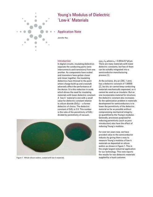
Figure 1. Whole silicon wafers, coated with low-k materials.<br />
Introduction<br />
In digital circuits, insulating dielectrics<br />
separate the conducting parts (wire<br />
interconnects and transistors) from one<br />
another. As components have scaled<br />
and transistors have gotten closer<br />
and closer together, the insulating<br />
dielectrics have thinned to the point<br />
where charge build up and crosstalk<br />
adversely affect the performance of<br />
the device. It is this reduction in scale<br />
which drives the need for insulating<br />
materials with lower dielectric constant.<br />
A ‘low-k’ material is one with a small<br />
value for dielectric constant relative<br />
to silicon dioxide (SiO2)—a former<br />
dielectric of choice. The dielectric<br />
constant of SiO2 is 3.9. This number<br />
is the ratio of the permittivity of SiO2<br />
divided by permittivity of vacuum,<br />
eSiO2/e 0,where e 0 = 8.854x10 -6pFμm.<br />
There are many materials with lower<br />
dielectric constants, but few of them<br />
can be suitably integrated into a<br />
semiconductor manufacturing<br />
process [1].<br />
At the extreme, dry air (20C, 1 atm)<br />
has a dielectric constant of 1.00059<br />
[2], but dry air cannot keep conducting<br />
materials mechanically separated, so it<br />
cannot be used as an insulator. But as<br />
one incorporates material for structure,<br />
the dielectric constant also increases.<br />
So the optimization problem in materials<br />
development for semiconductors is to<br />
lower the permittivity of the dielectric<br />
material as far as possible without<br />
compromising mechanical integrity,<br />
as quantified by the Young’s modulus.<br />
Generally, processes purposed for<br />
reducing permittivity (such as pore<br />
introduction) also have the effect of<br />
reducing Young’s modulus.<br />
For over ten years now, we have<br />
provided value to the semiconductor<br />
industry by giving them a way to<br />
measure Young’s modulus of low-k<br />
materials as deposited on silicon<br />
wafers as shown in Figure 1. This is<br />
the single largest industrial application<br />
for our technology. This note reports<br />
the results for two dielectric materials<br />
supplied by a loyal customer.