Cadence Chip Optimizer Datasheet - Cadence Design Systems
Cadence Chip Optimizer Datasheet - Cadence Design Systems Cadence Chip Optimizer Datasheet - Cadence Design Systems
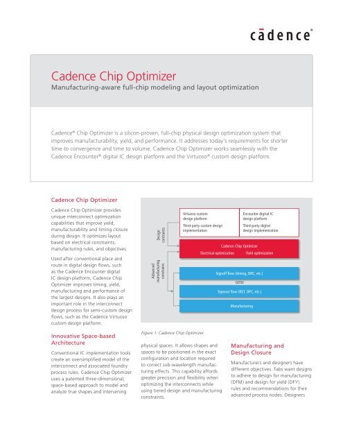
Cadence Chip Optimizer Manufacturing-aware full-chip modeling and layout optimization Cadence ® Chip Optimizer is a silicon-proven, full-chip physical design optimization system that improves manufacturability, yield, and performance. It addresses today’s requirements for shorter time to convergence and time to volume. Cadence Chip Optimizer works seamlessly with the Cadence Encounter ® digital IC design platform and the Virtuoso ® custom design platform. Cadence Chip Optimizer Cadence Chip Optimizer provides unique interconnect optimization capabilities that improve yield, manufacturability and timing closure during design. It optimizes layout based on electrical constraints, manufacturing rules, and objectives. Used after conventional place and route in digital design flows, such as the Cadence Encounter digital IC design platform, Cadence Chip Optimizer improves timing, yield, manufacturing and performance of the largest designs. It also plays an important role in the interconnect design process for semi-custom design flows, such as the Cadence Virtuoso custom design platform. Innovative Space-based Architecture Conventional IC implementation tools create an oversimplified model of the interconnect and associated foundry process rules. Cadence Chip Optimizer uses a patented three-dimensional, space-based approach to model and analyze true shapes and intervening Design contraints Advanced manufacturing constrains Virtuoso custom design platform Third-party custom design implementation Figure 1: Cadence Chip Optimizer physical spaces. It allows shapes and spaces to be positioned in the exact configuration and location required to correct sub-wavelength manufacturing effects. This capability affords greater precision and flexibility when optimizing the interconnects while using tiered design and manufacturing constraints. Encounter digital IC design platform Third-party digital design implementation Cadence Chip Optimizer Electrical optimization Yield optimization Signoff flow (timing, DRC, etc.) GDSII Tapeout flow (RET, OPC, etc.) Manufacturing Manufacturing and Design Closure Manufacturers and designers have different objectives. Fabs want designs to adhere to design for manufacturing (DFM) and design for yield (DFY) rules and recommendations for their advanced process nodes. Designers
- Page 2 and 3: Figure 2: Cadence Chip Optimizer im
<strong>Cadence</strong> <strong>Chip</strong> <strong>Optimizer</strong><br />
Manufacturing-aware full-chip modeling and layout optimization<br />
<strong>Cadence</strong> ® <strong>Chip</strong> <strong>Optimizer</strong> is a silicon-proven, full-chip physical design optimization system that<br />
improves manufacturability, yield, and performance. It addresses today’s requirements for shorter<br />
time to convergence and time to volume. <strong>Cadence</strong> <strong>Chip</strong> <strong>Optimizer</strong> works seamlessly with the<br />
<strong>Cadence</strong> Encounter ® digital IC design platform and the Virtuoso ® custom design platform.<br />
<strong>Cadence</strong> <strong>Chip</strong> <strong>Optimizer</strong><br />
<strong>Cadence</strong> <strong>Chip</strong> <strong>Optimizer</strong> provides<br />
unique interconnect optimization<br />
capabilities that improve yield,<br />
manufacturability and timing closure<br />
during design. It optimizes layout<br />
based on electrical constraints,<br />
manufacturing rules, and objectives.<br />
Used after conventional place and<br />
route in digital design flows, such<br />
as the <strong>Cadence</strong> Encounter digital<br />
IC design platform, <strong>Cadence</strong> <strong>Chip</strong><br />
<strong>Optimizer</strong> improves timing, yield,<br />
manufacturing and performance of<br />
the largest designs. It also plays an<br />
important role in the interconnect<br />
design process for semi-custom design<br />
flows, such as the <strong>Cadence</strong> Virtuoso<br />
custom design platform.<br />
Innovative Space-based<br />
Architecture<br />
Conventional IC implementation tools<br />
create an oversimplified model of the<br />
interconnect and associated foundry<br />
process rules. <strong>Cadence</strong> <strong>Chip</strong> <strong>Optimizer</strong><br />
uses a patented three-dimensional,<br />
space-based approach to model and<br />
analyze true shapes and intervening<br />
<strong>Design</strong><br />
contraints<br />
Advanced<br />
manufacturing<br />
constrains<br />
Virtuoso custom<br />
design platform<br />
Third-party custom design<br />
implementation<br />
Figure 1: <strong>Cadence</strong> <strong>Chip</strong> <strong>Optimizer</strong><br />
physical spaces. It allows shapes and<br />
spaces to be positioned in the exact<br />
configuration and location required<br />
to correct sub-wavelength manufacturing<br />
effects. This capability affords<br />
greater precision and flexibility when<br />
optimizing the interconnects while<br />
using tiered design and manufacturing<br />
constraints.<br />
Encounter digital IC<br />
design platform<br />
Third-party digital<br />
design implementation<br />
<strong>Cadence</strong> <strong>Chip</strong> <strong>Optimizer</strong><br />
Electrical optimization Yield optimization<br />
Signoff flow (timing, DRC, etc.)<br />
GDSII<br />
Tapeout flow (RET, OPC, etc.)<br />
Manufacturing<br />
Manufacturing and<br />
<strong>Design</strong> Closure<br />
Manufacturers and designers have<br />
different objectives. Fabs want designs<br />
to adhere to design for manufacturing<br />
(DFM) and design for yield (DFY)<br />
rules and recommendations for their<br />
advanced process nodes. <strong>Design</strong>ers
Figure 2: <strong>Cadence</strong> <strong>Chip</strong> <strong>Optimizer</strong> improves manufacturability and performance by<br />
optimizing interconnect layers<br />
want to achieve the greatest performance<br />
while performing the least amount of<br />
guard-banding. Schedules and predictability<br />
are also paramount concerns for<br />
designers.<br />
A common misconception is that these<br />
manufacturing and design objectives are<br />
always in opposition. However there is<br />
often a mutually agreeable solution. By<br />
optimizing wires (space and width), for<br />
example, designers can reduce the probability<br />
of opens and shorts (which is good<br />
for yield) while also reducing coupling<br />
capacitance (which is good for signal<br />
integrity, timing and power).<br />
With the powerful analysis and topology<br />
optimization capabilities provided by<br />
<strong>Cadence</strong> <strong>Chip</strong> <strong>Optimizer</strong>, designers can<br />
quickly achieve convergence that addresses<br />
both manufacturing and design objectives.<br />
Benefits<br />
• Addresses both DFY and DFM issues<br />
much earlier in the design flow<br />
– Faster geometric, electrical, and<br />
manufacturing convergence<br />
– Improves design margins and reduces<br />
guard-banding<br />
– Electrically (e.g., timing) correct design<br />
eliminates convergence iterations<br />
– Faster, more reliable ramp to volume<br />
silicon with up to six points of yield<br />
improvement<br />
• Innovative approach handles the most<br />
sophisticated geometries and constraints<br />
– True hierarchical, three-dimensional<br />
space-based approach enables<br />
accurate and precise modeling and<br />
optimizations<br />
– Architected to handle complex and<br />
tiered rules and constraints from<br />
90nm and below<br />
– Powerful topological changes ensure<br />
greatest manufacturability and<br />
performance gains<br />
• Silicon proven<br />
– Proven on high-volume and<br />
high-performance silicon at 130, 180,<br />
90, and 65nm process nodes<br />
• Easily adopted<br />
– Works seamlessly with the <strong>Cadence</strong><br />
Encounter and the Virtuoso platforms<br />
– Works with third-party implementation<br />
flows through industrystandard<br />
interfaces<br />
– Runs natively on OpenAccess<br />
Features<br />
<strong>Cadence</strong> <strong>Chip</strong> <strong>Optimizer</strong><br />
Manufacturability and yield<br />
enhancements<br />
• Optimizes vias to reduce via failures<br />
due to process window variability or<br />
misalignment. Enhancements include<br />
total via count reduction, adding multiple<br />
vias, optimizing enclosures and spacing<br />
• Optimizes wires to reduce wire<br />
failures due to isolated lines (opens) or<br />
minimum spaced lines (shorts)<br />
• Optimizes metal to minimize chemical<br />
mechanical polishing (CMP) effects<br />
• Eliminates process antennas<br />
• Increases manufacturability and RET<br />
efficiency by optimizing wire topologies<br />
<strong>Design</strong> closure enhancements<br />
• Connectivity and design rules are<br />
omnipresent for correct-by-construction<br />
editing<br />
• Wire push capability “pushes”<br />
neighboring wires to optimally fit a new<br />
wire and still meet design rules<br />
• Improves design margins and reduces<br />
guard-banding<br />
• Reduces total and coupling capacitance<br />
inline with timing and power objectives<br />
• Power and ground optimization<br />
Unparalleled speed and capacity<br />
• Offers speed and high-capacity through<br />
the use of new (patented) hierarchical<br />
modeling and search algorithms<br />
• Multithreaded operation<br />
Fully integrated check and analysis<br />
• Supports sophisticated recommended rules<br />
and constraints from 90nm and below<br />
• Fast and accurate interactive DRC and<br />
connectivity (open/short) checking<br />
• Browser to analyze optimization and<br />
verification results<br />
• Critical areas (defect limited yield<br />
sensitive areas) are identified using<br />
critical area analysis techniques<br />
www.cadence.com 2
Full-featured navigation system<br />
• Aerial view window provides full-chip<br />
navigation context<br />
• Query engine enables powerful<br />
searches of layout data<br />
• <strong>Design</strong>ers can fully tune the desired<br />
layers, layer-purposes and transparency<br />
for display and selection<br />
• Useful views and environment contexts<br />
can be bookmarked and saved<br />
Easy to learn, use, and extend<br />
• Provides an intuitive windowing system<br />
and command set<br />
• Extensive TCL programming interface<br />
Specifications<br />
Inputs<br />
• OpenAccess, XML, LEF DEF, GDSII, CDB,<br />
SPEF, Timing Libraries and Constraints<br />
Outputs<br />
• OpenAccess, XML, LEF DEF, GDSII<br />
Platforms<br />
• Sun Solaris (32-bit, 64-bit)<br />
• Linux (32-bit, 64-bit)<br />
• IBM AIX (32-bit, 64-bit)<br />
<strong>Cadence</strong> Services and Support<br />
• <strong>Cadence</strong> application engineers can<br />
answer your technical questions by<br />
telephone, email, or Internet—they can<br />
also provide technical assistance and<br />
custom training<br />
• <strong>Cadence</strong> certified instructors teach<br />
more than 70 courses and bring<br />
their real-world experience into the<br />
classroom<br />
• More than 25 Internet Learning<br />
Series (iLS) online courses allow you<br />
the flexibility of training at your own<br />
computer via the Internet<br />
• <strong>Cadence</strong> Online Support gives you 24x7<br />
online access to a knowledgebase of<br />
the latest solutions, technical documentation,<br />
software downloads, and more<br />
<strong>Cadence</strong> <strong>Chip</strong> <strong>Optimizer</strong><br />
<strong>Cadence</strong> is transforming the global electronics industry through a vision called EDA360.<br />
With an application-driven approach to design, our software, hardware, IP, and services help<br />
customers realize silicon, SoCs, and complete systems efficiently and profitably. www.cadence.com<br />
©2012 <strong>Cadence</strong> <strong>Design</strong> <strong>Systems</strong>, Inc. All rights reserved. <strong>Cadence</strong>, the <strong>Cadence</strong> logo, Encounter, and Virtuoso are registered trademarks of <strong>Cadence</strong><br />
<strong>Design</strong> <strong>Systems</strong>, Inc. All others are properties of their respective holders. 20630 1/12 KM/MVC/CS/PDF


