nokia morph technology - 123seminarsonly.com
nokia morph technology - 123seminarsonly.com
nokia morph technology - 123seminarsonly.com
Create successful ePaper yourself
Turn your PDF publications into a flip-book with our unique Google optimized e-Paper software.
Seminar<br />
on<br />
NOKIA MORPH TECHNOLOGY
SEMINAR REPORT<br />
ON<br />
“NOKIA MORPH TECHNOLOGY”<br />
BY<br />
SURESH KUMAR LALCHANDANI<br />
EXAM SEAT NO. T3444343<br />
CLASS: T.E. COMPUTER ENGINEERING<br />
YEAR: 2009- 2010<br />
DEPARTMENT OF COMPUTER ENGINEERING<br />
UNDER THE GUIDANCE OF<br />
PROF.SUSHAMA SHINDE<br />
CAYMET’S<br />
SIDDHANT COLLEGE OF ENGINEERING<br />
SUDUMBARE, MAVAL, PUNE-412109
C.A.Y.M.E.T’S<br />
SIDDHANT COLLEGE OF ENGINEERING<br />
SUDUMBARE ,MAVAL,PUNE(MAHARASHTRA)-412109<br />
Department of Computer Engineering<br />
CERTIFICATE<br />
This is to certify that Mr. SURESH KUMAR LALCHANDANI,T-3444343 has<br />
successfully <strong>com</strong>pleted seminar on “NOKIA MORPH TECHNOLOGY” as partial<br />
fulfillment of term work for Third year Computer Engineering in Semester-II for the<br />
academic year 2009-2010.<br />
(Prof. Shinde Sushama.)<br />
Seminar Guide<br />
(Prof. Kumbharkar P.B.)<br />
H.O.D.<br />
(Prof. Patole Mrunalini)<br />
Seminar Co-ordinatore<br />
(Dr. Sontakke T.R.)<br />
Principal
ACKNOWLEDGEMENT<br />
I take this humble opportunity to express my deep sense of gratitude to my<br />
seminar guide Prof. SUSHAMA SHINDE, who in all respect helped me tangibly from<br />
the beginning till the fulfillment of my seminar .His expert guidance and inspiration<br />
brought <strong>com</strong>pletion of the seminar.<br />
I would like to thank Prof.P.B.Kumbharkar, Head of Computer Engineering<br />
Department, who gives me this opportunity. I would also like to thank to all my<br />
teachers who directly or indirectly supports me time to time.<br />
Last but not least I would like to express a deep sense of gratitude from the<br />
bottom of my heart to my parents, without whom it was impossible for me to reach at<br />
this stage.<br />
Thank you & Regards.<br />
SURESH KUMAR LALCHANDANI
Abstract<br />
Contents<br />
1.0 INTRODUCTION 9<br />
1.0.1 What is a <strong>morph</strong>? 9<br />
1.1 History 10<br />
1.2 About<br />
1.2.1 Nokia Morph 12<br />
1.2.2 NanoTechnology 12<br />
1.2.3 Molecular Nano<strong>technology</strong> 12<br />
1.2.4 Collaboration 13<br />
1.2.5 Univaersity of cambridge 14<br />
1.2.6 Nokia Research Center 15<br />
2.0 THEORY<br />
2.1 Concepts of <strong>nokia</strong> <strong>morph</strong> 17<br />
2.2 Applied Technology 18<br />
2.3 Various Nanotechnologies 19<br />
2.3.1 Nano-enabled energy 20<br />
2.3.1.1 Enhanced enabled energy 20<br />
2.3.1.1.1 Density batteries 20<br />
2.3.1.1.2 Supercapacitors 20<br />
2.3.1.1.3 Solar Research 20<br />
2.3.1.1.4 NEMS structure 21<br />
2.3.2 Sensing surfaces 21<br />
2.3.2.1 Nanoscale Benefits 22<br />
2.3.2.2 Our Research Focus 22<br />
2.3.3 Stretchable Electronic 23<br />
2.3.4 Functional Biomaterials 25<br />
2.3.5 Nanoporous Hybrid Material 26<br />
2.3.6 Device Architecture 27
3.0 FEATURES & CHARACTERSTICS<br />
3.1 Flexiblity and changing Design 29<br />
3.2 Self Cleaning 30<br />
3.3 Advance power Resources 31<br />
3.4 Sensing the environment 32<br />
4.0 WORKING AREA OF NOKIA MORPH<br />
4.1 New trends are evolving 33<br />
5.0 CONCLUSION 35<br />
REFRENCES 36
1.1 Nano Flower<br />
1.2 Nano Scince Center<br />
1.3 Nokia research center<br />
2.1 Phone mode snap<br />
2.2 10 nm Anio & Cation<br />
2.3 Solar cell capacitor<br />
2.4 Circuit diagram for solar cell<br />
2.5 Sensing surfaces and system<br />
2.6 Nano wires<br />
2.7 ZnO Nanowires<br />
2.8 Biological Effects<br />
3.1 Various Shapes<br />
3.2 NanoFlower Zoom Snap<br />
3.3 Nano Grass<br />
4.1 Various Tasking<br />
4.2 Multifunctionality<br />
FIGURES INDEX<br />
Name of figures Page no<br />
12<br />
15<br />
17<br />
18<br />
20<br />
21<br />
22<br />
23<br />
24<br />
25<br />
27<br />
29<br />
30<br />
31<br />
32
ABSTRACT<br />
NOKIA MORPH TECHNOLOGY<br />
SURESH KUMAR LALCHANDANI<br />
Siddhant College of Engineering<br />
University of Pune<br />
E-mail:Suresh.chandani@live.<strong>com</strong><br />
In business a product could have a shorter life if it can't win the hearts of people and<br />
showcase new <strong>technology</strong>, so take the case of Nokia, who is <strong>com</strong>ing up with the Nokia<br />
Morph flexible mobile phone which the <strong>com</strong>pany claims include nano<strong>technology</strong> and<br />
would immensely benefit its end-users. The main benefit of Nano<strong>technology</strong> is that its<br />
<strong>com</strong>ponents are flexible, transparent and extremely strong. The <strong>com</strong>pany believes this<br />
latest <strong>technology</strong> would be a distinctive phone by 2015, but a few technical glitches<br />
remained to be solved, like the use of new battery materials etc.<br />
Nokia <strong>morph</strong> is a joint <strong>technology</strong> concept, developed by <strong>nokia</strong> research center (NRC)<br />
and the University of Cambridge (UK). The <strong>morph</strong> demonstrate how future mobile<br />
device might be stretchable and flexible, allowing the user to transform their mibile<br />
devices into radically different shaped . It demonstrate the ultimately that nano<strong>technology</strong><br />
might be capable of delivering: flexible material, transparent electrononcs and self-<br />
cleaning surface.<br />
Nano<strong>technology</strong> enables materials and <strong>com</strong>ponents that are flexible,stretchable,<br />
transparent and remarkably strong. Fibril proteins are woven into three dimensional mesh<br />
that reinforces thin elastic structures.Using the same principle behind spider silk, this<br />
elasticity enables the device to literally changes shapes and configure itself to adapt to the<br />
task at hand.
CHAPTER 1<br />
INTRODUCTION<br />
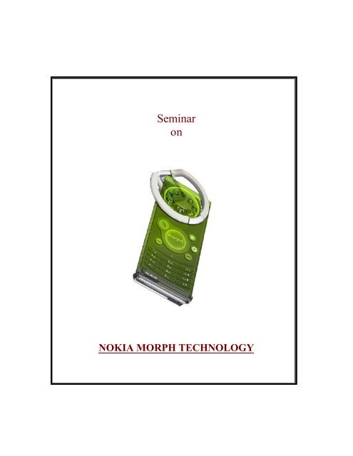
The Morph concept<br />
Launched alongside The Museum of Modern Art “Design and The Elastic Mind”<br />
exhibition, the Morph concept device is a bridge between highly advanced technologies<br />
and their potential benefits to end-users. This device concept showcases some<br />
revolutionary leaps being explored by Nokia Research Center (NRC) in collaboration<br />
with the Cambridge Nanoscience Centre (United Kingdom) – nanoscale technologies that<br />
will potentially create a world of radically different devices that open up an entirely new<br />
spectrum of possibilities.<br />
Morph concept technologies might create fantastic opportunities for mobile devices:<br />
• Newly-enabled flexible and transparent materials blend more seamlessly with the<br />
way we live<br />
• Devices be<strong>com</strong>e self-cleaning and self-preserving<br />
• Transparent electronics offering an entirely new aesthetic dimension<br />
• Built-in solar absorption might charge a device, whilst batteries be<strong>com</strong>e smaller,<br />
longer lasting and faster to charge<br />
• Integrated sensors might allow us to learn more about the environment around us,<br />
empowering us to make better choices<br />
In addition to the advances above, the integrated electronics shown in the Morph concept<br />
could cost less and include more functionality in a much smaller space, even as interfaces<br />
are simplified and usability is enhanced. All of these new capabilities will unleash new<br />
applications and services that will allow us to <strong>com</strong>municate and interact in unprecedented<br />
ways.
1.1 HISTORY<br />
I remember when the Apple iPhone came out. I had a deep sense that there was no<br />
way I’d buy a normal mobile phone ever again. I also started thinking: what <strong>com</strong>es next?<br />
Well it looks like I’ve found the answer over at Nokia HQ. In fact, if you are in New<br />
York you can go along and see the future of mobile phones right now at The Museum of<br />
Modern Art. Nokia Research Centre and the University of .3.Cambridge’s Nanoscience<br />
Centre have launched Morph, a joint nanotech concept. This device concept showcases<br />
some revolutionary leaps being explored by Nokia Research Center (NRC) in<br />
collaboration with the Cambridge Nanoscience Centre (United Kingdom) – Nanoscale<br />
technologies that will potentially create a world of radically different devices that open<br />
up an entirely new spectrum of possibilities.<br />
• Invitation to contribute to Museum of Modern Art (MoMA) in April 2007<br />
• Brainstorming in Cambridge in June 2007; Nokia Research Centre, Nokia Design and<br />
University of Cambridge<br />
• First concepts to MoMA in August 2007.<br />
• MoMA exhibition in February 2008<br />
1.2 ABOUT<br />
1.2.1 Nokia Morph<br />
Morph is a concept that demonstrates how future mobile devices might be stretchable<br />
and flexible, allowing the user to transform their mobile device into radically different<br />
shapes. It demonstrates the ultimate functionality that nano<strong>technology</strong> might be capable<br />
of delivering: flexible materials, transparent electronics and self-cleaning surfaces.The<br />
device, which is made using nano<strong>technology</strong>, is intended to demonstrate how cell phones<br />
in the future could be stretched and bent into different shapes, allowing users to “<strong>morph</strong>”<br />
their devices into whatever shape they want. Want to wear your cell phone as a bracelet?<br />
No problem, just bend it around your wrist.
Even though Morph is still in early development, Nokia believes that certain elements<br />
of the device could be used in high-end Nokia devices within the next seven years. And<br />
as the <strong>technology</strong> matures, nano<strong>technology</strong> could eventually be incorporated into Nokia’s<br />
entire line of products to help lower manufacturing costs. Nokia Morph is truly an<br />
absolutely wonderful gadget with flexible bending and wearing options and surely the<br />
best in the gadgets segment from the house of Nokia<br />
1.2.2 What is Nano<strong>technology</strong>?<br />
A basic definition: Nano<strong>technology</strong> is the engineering of functional systems at the<br />
molecular scale. This covers both current work and concepts that are more advanced.<br />
In its original sense, 'nano<strong>technology</strong>' refers to the projected ability to construct items<br />
from the bottom up, using techniques and tools being developed today to make <strong>com</strong>plete,<br />
high performance products.<br />
Nano<strong>technology</strong> may one day lead to low cost manufacturing solutions, and offers<br />
the possibility of integrating <strong>com</strong>plex functionality at a low price. Nano<strong>technology</strong> also<br />
can be leveraged to create self-cleaning surfaces on mobile devices, ultimately reducing<br />
corrosion, wear and improving longevity. Nanostructured surfaces, such as<br />
“Nanoflowers” naturally repel water, dirt, and even fingerprints utilizing effects also seen<br />
in natural systems.<br />
Figure 1.1 A Nano Flower<br />
Elegant three-dimensional MoS2 nanoflowers were uniformly formed via heating<br />
a MoO2 thin film in a vapor sulfur atmosphere. Tens to hundreds of petals were self-
assembled within a single nanoflower. Each petal, 100–300 nm wide and only several<br />
nanometers thick, exhibited a hexagonal structure. The number of petal layers gradually<br />
decreased towards the edges, resulting in uniquely thin edges, typically less than 3 nm.<br />
The MoS2 nanoflowers appeared to be excellent field emitters displaying a current<br />
density of 0.01 and 10? mA/cm 2 at macroscopic fields of 4.5–5.5 and 7.6–8.6 V/µm,<br />
respectively; the electron field emission was consistent with the Fowler–Nordheim<br />
theory.<br />
1.2.3 Molecular nano<strong>technology</strong>:<br />
Molecular nano<strong>technology</strong>, sometimes called molecular manufacturing, describes<br />
engineered nanosystems (nanoscale machines) operating on the molecular scale.<br />
Molecular nano<strong>technology</strong> is especially associated with the molecular assembler, a<br />
machine that can produce a desired structure or device atom-by-atom using the principles<br />
of mechanosynthesis. Manufacturing in the context of productive nanosystems is not<br />
related to, and should be clearly distinguished from, the conventional technologies used<br />
to manufacture nanomaterials such as carbon nanotubes and nanoparticles.<br />
When the term "nano<strong>technology</strong>" was independently coined and popularized by Eric<br />
Drexler (who at the time was unaware of an earlier usage by Norio Taniguchi) it referred<br />
to a future manufacturing <strong>technology</strong> based on molecular machine systems. The premise<br />
was that molecular scale biological analogies of traditional machine <strong>com</strong>ponents<br />
demonstrated molecular machines were possible: by the countless examples found in<br />
biology, it is known that sophisticated, stochastically optimised biological machines can<br />
be produced..<br />
It is hoped that developments in nano<strong>technology</strong> will make possible their construction by<br />
some other means, perhaps using biomimetic principles. However, Drexler and other<br />
researchers [6] have proposed that advanced nano<strong>technology</strong>, although perhaps initially<br />
implemented by biomimetic means, ultimately could be based on mechanical engineering<br />
principles, namely, a manufacturing <strong>technology</strong> based on the mechanical functionality of<br />
these <strong>com</strong>ponents (such as gears, bearings, motors, and structural members) that would
enable programmable, positional assembly to atomic specification. [7] The physics and<br />
engineering performance of exemplar designs were analyzed in Drexler's book<br />
Nanosystems.<br />
In general it is very difficult to assemble devices on the atomic scale, as all one has to<br />
position atoms are other atoms of <strong>com</strong>parable size and stickiness. Another view, put forth<br />
by Carlo Montemagno, [8] is that future nanosystems will be hybrids of silicon <strong>technology</strong><br />
and biological molecular machines. Yet another view, put forward by the late Richard<br />
Smalley, is that mechanosynthesis is impossible due to the difficulties in mechanically<br />
manipulating individual molecules.<br />
This led to an exchange of letters in the ACS publication Chemical & Engineering News<br />
in 2003. [9] Though biology clearly demonstrates that molecular machine systems are<br />
possible, non-biological molecular machines are today only in their infancy. Leaders in<br />
research on non-biological molecular machines are Dr. Alex Zettl and his colleagues at<br />
Lawrence Berkeley Laboratories and UC Berkeley. They have constructed at least three<br />
distinct molecular devices whose motion is controlled from the desktop with changing<br />
voltage: a nanotube nanomotor, a molecular actuator, [10] and a nanoelectromechanical<br />
relaxation oscillator. [11]<br />
An experiment indicating that positional molecular assembly is possible was performed<br />
by Ho and Lee at Cornell University in 1999. They used a scanning tunneling microscope<br />
to move an individual carbon monoxide molecule (CO) to an individual iron atom (Fe)<br />
sitting on a flat silver crystal, and chemically bound the CO to the Fe by applying a<br />
voltage.<br />
1.2.4 Collaboration Between NRC and University of Cambridge<br />
The partnership between Nokia and the University of Cambridge was announced in<br />
March, 2007 - an agreement to work together on an extensive and long term programme<br />
of joint research projects. NRC has established a research facility at the University's<br />
West Cambridge site and collaborates with several departments - initially the
Nanoscience Center and Electrical Division of the Engineering Department - on projects<br />
that, to begin with, are centered on nano<strong>technology</strong>.<br />
With the ability of the phone to take on a variety of shapes and sizes, most people may<br />
not need to change phones so often as they currently have been doing so every 1.5 years<br />
on average. According to Nokia, it would take seven years before Morph phones are<br />
available at consumer markets.<br />
The Morph concept <strong>technology</strong> carries numerous interesting features for future mobile<br />
evices.<br />
1. Newly-enabled flexible transparent materials blend more seamlessly with the<br />
way we live.<br />
2. Devices be<strong>com</strong>e self-cleaning and self-preserving.<br />
3. Transparent electronics offering an entirely new aesthetic dimension.<br />
4. Built-in solar absorption might charge a device, whilst batteries be<strong>com</strong>e smaller,<br />
longer lasting and faster to charge.<br />
5. Integrated sensors might allow us to learn more about the environment around<br />
us, empowering us to make better choices.<br />
In addition to the advances above, the integrated electronics would cost less and include<br />
more functionality in a much smaller space, even as interfaces are simplified and<br />
usability is enhanced.<br />
Mobile phones like Nano Morph certainly depict the up<strong>com</strong>ing Nano Technology<br />
and it will surely be a front-runner in the use of various gadgets and technologies be it<br />
Computers, Air Conditioners, Robots, Cars or like this one viz Mobile phones and<br />
smartphones.<br />
1.2.5 About University of Cambridge Nano Research Center<br />
In Nanoscience Centre is an 1800m² research facility <strong>com</strong>pleted in January 2003 and<br />
located at the north east corner of the University's West Cambridge Site. The Centre<br />
provides open access to over 300 researchers from a variety of University Departments to<br />
the nanofabrication and characterisation facilities housed in a <strong>com</strong>bination of Clean
Rooms and low noise laboratories. Office space is primarily home to the Department of<br />
Engineering’s Nanoscience Group, technical and administrative staff and members of<br />
other research groups who require long term access to facilities.<br />
The partnership between Nokia and the University of Cambridge was announced in<br />
March, 2007 - an agreement to work together on an extensive and long term programme<br />
of joint research projects. NRC has established a research facility at the University's West<br />
Cambridge site and collaborates with several departments - initially the Nanoscience<br />
Center and Electrical Division of the Engineering Department - on projects that, to begin<br />
with, are centered on nano<strong>technology</strong>.<br />
1.2.6 Nokia Research Center<br />
Figure 1.2 The Nano Center<br />
Nokia believes that effective research and development is vital to remaining <strong>com</strong>petitive<br />
in the mobile <strong>com</strong>puting and <strong>com</strong>munications industry. As of April 1, 2007, we had R&D<br />
centers in 11 countries and employed 14,500 people in research and development,<br />
representing approximately 32% of Nokia’s total workforce. R&D expenses totaled EUR<br />
3,9 billion in 2006, representing 9,5% of Nokia’s net sales. We invest a substantial<br />
portion of our resources in research and development activities within our principal<br />
business groups Mobile Phones, Multimedia and Enterprise Solutions, Technology<br />
Platforms , and in the Nokia Research Center (NRC).<br />
Nokia Research Center has a unique mission to lead Nokia into the future: NRC will be<br />
the global leader of open innovation for human mobility systems of the fused physical<br />
and digital world, giving birth to the growth of businesses for Nokia.
Nokia Research Center was founded in 1986 from the Nokia Electronics R&D unit, with<br />
the a headcount of 86 persons. Today, NRC employs roughly 800 researchers from 43<br />
countires and a wide variety of fields. Representing just over 4% of Nokia’s R&D<br />
employees, NRC researchers produce about one half of Nokia’s essential patents, and<br />
34% of all Nokia invention reports (2006).<br />
NRC has a two-fold approach to achieving its mandate. The work for core <strong>technology</strong><br />
breakthroughs supporting Nokia's existing businesses takes place in the Core Technology<br />
Centers, the CTC's. More visionary, exploratory systems research that goes well beyond<br />
any current business model is conducted at the many System Research Centers, the<br />
SRC's.<br />
Figure 1.3 The Nokia research center
CHAPTER 2<br />
2.1 CONCEPT OF NOKIA MORPH<br />
Morph is a concept that demonstrates how future mobile devices might be stretchable and<br />
flexible, allowing the user to transform their mobile device into radically different shapes.<br />
It demonstrates the ultimate functionality that nano<strong>technology</strong> might be capable of<br />
delivering: flexible materials, transparent electronics and self-cleaning surfaces. Dr. Bob<br />
Iannucci, Chief Technology Officer, Nokia, <strong>com</strong>mented: "Nokia Research Center is<br />
looking at ways to reinvent the form and function of mobile devices; the Morph concept<br />
shows what might be possible".<br />
Figure 2.1 Phone Mode Snap<br />
Professor Mark Welland, Head of the Department of Engineering's Nanoscience Group at<br />
the University of Cambridge and University Director of Nokia-Cambridge collaboration<br />
added: "Developing the Morph concept with Nokia has provided us with a focus that is<br />
both artistically inspirational but, more importantly, sets the <strong>technology</strong> agenda for our<br />
joint nanoscience research that will stimulate our future work together."
2.2 APLLIED TECHNOLOGY USED<br />
NANOTECHNOLOGY<br />
Nano<strong>technology</strong> may one day lead to low cost manufacturing solutions, and offers<br />
the possibility of integrating <strong>com</strong>plex functionality at a low price. Nano<strong>technology</strong> also<br />
can be leveraged to create self-cleaning surfaces on mobile devices, ultimately reducing<br />
corrosion, wear and improving longevity. Nanostructured surfaces, such as<br />
“Nanoflowers” naturally repel water, dirt, and even fingerprints utilizing effects also seen<br />
in natural systems.<br />
Professor Mark Welland, Head of the Department of Engineering's Nanoscience<br />
Group at the University of Cambridge and University Director of Nokia-Cambridge<br />
collaboration added: "Developing the Morph concept with Nokia has provided us with a<br />
focus that is both artistically inspirational but, more importantly, sets the <strong>technology</strong><br />
agenda for our joint nanoscience research that will stimulate our future work together."<br />
Nano Technology has evolved as an all together different <strong>technology</strong> area in the mobile<br />
world. Mobile phones are advancing at a great and faster pace than never before and<br />
Nokia Morph is truly a mobile wonder. This phone has been developed by Nokia<br />
Research Center and the University of Cambridge. Mobile phones like Nano Morph<br />
certainly depict the up<strong>com</strong>ing Nano Technology and it will surely be a front-runner in the<br />
use of various gadgets and technologies be it Computers, Air Conditioners, Robots, Cars<br />
or like this one viz Mobile phones and smartphones. Nokia Morph is truly an absolutely<br />
wonderful gadget with flexible bending and wearing options and surely the best in the<br />
gadgets segment from the house of Nokia. Wonder what will be next from Nokia,<br />
World’s leader in the Communication segment.<br />
It would also feature self-cleaning to prevent wear and tear based on nanostructures<br />
called ‘Nano flowers’ which do not absorb liquids or retain fingerprints. The Nokia<br />
Morph phone would also include a detachable speaker that could clip onto the ear or<br />
connect to the phone as a speaker. In addition, the battery is solar powered with built in
self-charging high density solar charging modules called Nanograss which are capable of<br />
recharging faster than any other battery solution.<br />
Morph phones would have Nanosensors to inform users of wireless environments and<br />
enable them to make choices on the available wireless networks. The phones would also<br />
be able to analyze the pollution levels of the environment and monitor the user’s<br />
surroundings.<br />
2..3 VARUIOUS NANOTECHNOLOGIES USED<br />
2.3.1 NANO-ENABLED ENERGY<br />
Nano<strong>technology</strong> holds out the possibility that the surface of a device will be<strong>com</strong>e<br />
a natural source of energy via a covering of “Nanograss” structures that harvest<br />
solar power. At the same time new high energy density storage materials allow<br />
batteries to be<strong>com</strong>e smaller and thinner, while also quicker to recharge and able<br />
to endure more charging cycles.<br />
2.3.1.1 ENHANCED ENERGY HARVESTING AND STORAGE<br />
2.3.1.1.1 ENHANCED ENERGY DENSITY BATTERIES<br />
– Nanostructured electrodes for very low equivalent series R energy sources<br />
– New electrolyte solutions (ionic liquids) for safe and high power batteries.<br />
Deformable and bendable structures.<br />
Figure 2.2 10 nm Anion and Cation for battery
2.3.1.1.2 SUPERCAPACITORS<br />
– Nanoenhanced dielectrics for separator and high power capacitors<br />
– Ultra thin flexible structures, for ultimately distributed energy storage,<br />
and integration with battery structures<br />
2.3.1.1.3 SOLAR CELL RESEARCH<br />
– Nanowire solar cells using nanowire networks<br />
– Silicon solar cell production for emerging markets as primary power<br />
Source<br />
2.3.1.1.4 ENERGY HARVESTING FROM RF USING WIDEBAND<br />
ANTENNAS, AND USING NEMS STRUCTURES<br />
– Microwatt level energy harvesting from ‘waste’ energy in the air<br />
- Charging battery from ultra low power energysources, and power<br />
management for that<br />
- Harvesting RF energy<br />
Figure 2.31 Solar Cell Capacitor Architecture
\<br />
2.3.2 SENSING SURFACES<br />
Nanosensors would empower users to examine the environment around them in<br />
<strong>com</strong>pletely new ways, from analyzing air pollution, to gaining insight into bio-chemical<br />
traces and processes. New capabilities might be as <strong>com</strong>plex as helping us monitor<br />
evolving conditions in the quality of our surroundings, or as simple as knowing if the<br />
fruit we are about to enjoy should be washed before we eat it. Our ability to tune into our<br />
environment in these ways can help us make key decisions that guide our daily actions<br />
and ultimately can enhance our health<br />
Figure 2.4 Circuit Diagram for Solar Cell<br />
Figure 2.51 Sensing surface and Graph
Characteristics for sensor applications<br />
• Uniaxial piezoelectric response<br />
• Enabler of novel touch sensor concepts<br />
• n-type semiconductor behaviour<br />
• Candidate for photovoltaics<br />
• Enables various low-cost applications<br />
2.3.2.1 NANOSCALE BENEFITS<br />
• The Huge Array of parallel sensors that can be either independently or<br />
collectively measured<br />
• New sensor ssignal processing paradigm<br />
• New materials that can be used to improve sensors characterstic<br />
2.3.2.2 OUR RESEARCH FOCUS<br />
Stability, resolution, reliability & response time.<br />
o Nanoresonator based optical sensors<br />
o ZnO nanowire base stain sensors<br />
o New signal process method used for nano base <strong>com</strong>puting<br />
2.3.2.3 SMART SURFACES HUGE NUMBER OF NANOSENSORS WITH ANALOGUE<br />
INFORMATION PROCESSING BY NANOCOMPUTING, FEEDING PROPERLY PRE<br />
PROCESSED DATA OUT.<br />
2.3.3 STRETCHABLE ELECTRONICS<br />
Target:<br />
• Creation of stretchable devices<br />
– Embedded active electronics in elastic structures (sensors, actuators, circuitry)<br />
– Ordered nanoscale internal structures for controlling the elasticity<br />
– A pixellated, integrated system to withstand extreme deformations
– Minimal strain on rigid island platforms for sensitive <strong>com</strong>ponents<br />
– Stretchable electronics structures to allow reconfigurable device form factors.<br />
– Flexible electronics structures (interconnects, circuits and substrates) that sustain<br />
–<br />
>10% 2D strain<br />
ZnO Nanowires for flexible tactile arrays<br />
• Arrays of aligned zinc oxide nanowires grown hydrothermally from<br />
zinc salt precursor on the surface of substrates (at roughly 70 – 100 oC)<br />
• Economical and environmentally-friendly<br />
• Compatible with polymer substrates<br />
Figure 2.61 Nano woires
Nanowire Lithography<br />
Silicon Nanowires for Stretchable Electronics Combining top-down<br />
fabrication via SOI etching using masks made of nanowires grown by a<br />
bottom-up approach.<br />
Blue = Si; Grey = SiO2;<br />
Yellow = Metal (Ni)<br />
Highly-conducting SiNW networks via nanowire lithography (NWL): A. Colli, A. Fasoli,<br />
S. Pisana, Y. Fu, P. Beecher, W. I. Milne, A. C.<br />
Ferrari, Nano Letters 8, 1358 (2008)<br />
Figure 2.7 ZnO Nanowires<br />
Figure 2.8 Stretchable area
Figure 2.9 Patterned Zno nanowire array for tactile sensing – U of C / NRC<br />
Cambridge UK<br />
2.3.4 Functional Biomaterials<br />
There is a big demand for biomaterials to assist or replace organ functions and to improve<br />
patients’ quality of life. Materials options include metals, ceramics and polymers.<br />
Unfortunately, conventional materials are used that were<br />
not specifically developed for biological applications.Interaction between biomaterials<br />
and natural tissues is an important subject for biomaterial science Such information is<br />
essential to aid the design of new bio<strong>com</strong>patible biomaterials.<br />
Figure 2.10 Biological Effects<br />
The vision of ambient intelligence describes a network of sensors connected to one or<br />
more <strong>com</strong>puting devices. Sensors will be everywhere: in your pocket, in your faucet, in<br />
your refrigerator, at your front door, and in your running shoe. The device integrates data<br />
from your physical world, deduces patterns, identifies issues, consults with Internet
services, and responds with intelligence—seeming to anticipate your every need—all at<br />
the rapid pace of your daily life.<br />
• Computational Medicine and the Individual<br />
Start with inexpensive sensors that can be worn, implanted, or swallowed (as Feynman<br />
suggested in 1959). Marry them with data reduction capabilities that <strong>com</strong>pute trends and<br />
interactions to build a holistic personal medical profile. Equipped with this information,<br />
the individual’s mobile device can relay the diagnosis to health care resources,<br />
dispatching an ambulance automatically.<br />
2.3.5 Nanoporous Hybrid Materials<br />
Recently, the domain of nanoporous materials has been enlarged very much to the<br />
development of porous hybrid materials designated as metal-organic frameworks<br />
(MOF),1 porous coordination polymers2 or organic-inorganic hybrids3,4 which are the<br />
most recently highlighted class of materials consisting of metal ions linked together by<br />
organic bridging ligands in the framework. The attraction of <strong>com</strong>bining properties from<br />
both inorganic and organic <strong>com</strong>ponents has led to a quest of research toward new hybrid<br />
materials with potential applications including gas storage, catalysis, separation, and<br />
molecular recognition.1-4 Very recently, Férey and co-workers have repoted a novel<br />
hybrid material,chromium trimesate (designated as MIL-100), which has a hierarchical<br />
pore system (micro: 5-9 Å; mesoporous: 25-30 Å) with a very high Langmuir surface<br />
area.5
Figure 2.8<br />
Biological<br />
2.3.6 Device Architectures<br />
The Nano Devices team collaborates closely with researchers at the University<br />
of Cambridge, focussing on nanoscience research and its application to novel<br />
solutions in such diverse areas as sensing, energy storage/harvesting, novel<br />
<strong>com</strong>puting architectures, <strong>com</strong>munications <strong>technology</strong> and functional materials.<br />
Advances in all these fields will drive new device concepts and enable future<br />
ambient intelligence and wearable devices. As an example, the "Morph" design<br />
concept jointly developed by the University and NRC for the "Design and the<br />
Elastic Mind" exhibition at the New York Museum of Modern Art suggests how<br />
such nanotechnological developments may impact future mobile device form,<br />
function and use.<br />
• Connecting the Unconnected<br />
In developing nations, we see more basic (and potentially crucial) applications.<br />
The mobile device’s integrated sensors can monitor levels of pollutants,<br />
bacteria, and other environmental or health risks and notify officials when<br />
thresholds are exceeded. Also critical are point-of-care diagnostics and patient
monitoring— empowering health care providers to deliver on-the-spot treat-<br />
ment, informed by global Internet services and medical data banks.<br />
• New signal processing methods/devices<br />
The Nokia N900 is powered by a high-end OMAP 3430 ARM Cortex A8 which is<br />
a System-on-a-chip made by Texas Instruments based on a 65-nanometer CMOS process.<br />
The OMAP 3430 is <strong>com</strong>posed of three microprocessors; the Cortex A8 running at<br />
600 MHz used to run the OS and applications, the PowerVR SGX 530 GPU made<br />
by Imagination Technologies which supports OpenGL ES 2.0 and is capable of up to 14<br />
MPolys/s and a TMS320C64x, the digital signal processors, running at 430 MHz used to<br />
run the image processing (camera), audio processing (telephony) and data transmission.<br />
The TMS320 C64x main purpose is to offload the Cortex A8 from having to process<br />
audio and video signal. [29] The system has 256 MB of dedicated high performance RAM<br />
(Mobile DDR) paired with access to 768 MB swap space managed by the OS. [2] This<br />
provides a total of 1 GB of virtual memory
CHAPTER 3<br />
FEATURES AND CHARACTERSTICS<br />
3.1 Flexible & Changing Design<br />
Nano<strong>technology</strong> enables materials and <strong>com</strong>ponents that are flexible, stretchable,<br />
transparent and remarkably strong. Fibril proteins are woven into a three dimensional<br />
mesh that reinforces thin elastic structures. Using the same principle behind spider silk,<br />
this elasticity enables the device to literally ch ange shapes and configure itself to adapt<br />
to the task at hand.<br />
Figure 3.1 Various Shapes of Nokia Morph<br />
A folded design would fit easily in a pocket and could lend itself ergonomically to being<br />
used as a traditional handset. An unfolded larger design could display more detailed<br />
information, and incorporate input devices such as keyboards and touch pads.<br />
Even integrated electronics, from interconnects to sensors, could share these flexible<br />
properties. Further, utilization of biodegradable materials might make production and<br />
recycling of devices easier and ecologically friendly.
3.2 Self-Cleaning<br />
Nano<strong>technology</strong> also can be leveraged to create self-cleaning surfaces on mobile devices,<br />
ultimately reducing corrosion, wear and improving longevity. Nanostructured surfaces,<br />
such as “Nanoflowers” naturally repel water, dirt, and even fingerprints utilizing effects<br />
also seen in natural systems.<br />
A nanoflower, in chemistry, refers to a <strong>com</strong>pound of certain elements that results in<br />
formations which in microscopic view resemble flowers or, in some cases, trees that are<br />
called nanobouquets or nanotrees. [1] These formations are nanometers long and thick so<br />
they can only be observed using electron microscopy<br />
Nanoflowers” naturally repel water, dirt, and even fingerprints utilizing effects also seen<br />
in natural systems. That is why it is used for self cleaning purpose.<br />
Zinc oxide changes resistance when molecules of ethanol vapour stick onto it in a process<br />
called adsorption. The flower-like structures work at lower temperatures because their<br />
tiny size enhances adsorption. Each flower is made up of bundles of nanorods 15nm<br />
wide. They were made by blasting a zinc-containing solution with ultrasound.<br />
3.3 Advanced Power Sources<br />
Figure 3.2 Nano flowers Zoom snap
Nano<strong>technology</strong> holds out the possibility that the surface of a device will<br />
be<strong>com</strong>e a natural source of energy via a covering of “Nanograss” structures<br />
that harvest solar power. At the same time new high energy density storage<br />
materials allow batteries to be<strong>com</strong>e smaller and thinner, while also quicker<br />
to recharge and able to endure more charging cycles.<br />
Figure 3.3 Nano Grass for solar cell
3.4 Sensing The Environment<br />
Nanosensors would empower users to examine the environment around them in<br />
<strong>com</strong>pletely new ways, from analyzing air pollution, to gaining insight into bio-chemical<br />
traces and processes. New capabilities might be as <strong>com</strong>plex as helping us monitor<br />
evolving conditions in the quality of our surroundings, or as simple as knowing if the<br />
fruit we are about to enjoy should be washed before we eat it. Our ability to tune into our<br />
environment in these ways can help us make key decisions that guide our daily actions<br />
and ultimately can enhance our health<br />
Sensing surfaces using piezoelectric nanowire arrays<br />
ZnO exhibits an unusual <strong>com</strong>bination of properties, including uniaxial piezoelectric<br />
response and n-type semiconductor characteristics. Nokia is exploiting these qualities to<br />
achieve strain-based electromechanical transducers—ideal for touch-sensitive (even<br />
direction-sensitive) surfaces.<br />
Arrays of ZnO nanowires can be fabricated at low temperatures (roughly 70-100°C),<br />
providing <strong>com</strong>patibility with polymer substrates, such as polyethylene terephtalate (PET).<br />
By coating a substrate (silicon, glass, or PET) with an array of these ZnO nanowires, the<br />
electrical signals on the surface can be activated by mechanical force. Since ZnO<br />
nanowires and nanoparticles are nearly transparent, this technique can be used to develop<br />
<strong>com</strong>pliant, touch-sensitive, active matrix arrays that sit on top of displays or other<br />
structural elements.
CHAPTER 4<br />
WORKING AREA OF NOKIA MORPH<br />
4.1 NEW TRENDS ARE EVOLVING<br />
Flexible, stretchable, thin, transparent conformal devices - enabled by<br />
nano<strong>technology</strong><br />
Context aware device: adapts and transforms its functionality<br />
according to the tasks<br />
Wearable device<br />
• Available always and everywhere<br />
• New intuitive user interface<br />
• Flexible, <strong>com</strong>pliant and even stretchable structures are<br />
needed.<br />
• New power source technologies<br />
• Functional coatings<br />
How can we…<br />
… fabricate and manufacture innovative mechanical structures that can be both<br />
transparent and <strong>com</strong>pliant despite containing electronic and optical functions?<br />
… create a library of reliable and durable functional materials that enables a multitude of<br />
functions on the device surface, e.g., robust surfaces, EM shielding, dirt/water<br />
repellence, antenna integration, optical effects, touch sensors, haptics?
Figure 4.1 Various Works The <strong>morph</strong> DO<br />
Figure 4.2 Multi functional areas
CHAPTER 5<br />
CONCLUSION<br />
According to the developers, using nano<strong>technology</strong> can lead to low cost manufacturing<br />
solutions as well as adjustable, empowering devices, bringing us new, versatile<br />
possibilities. These mobile devices will be flexible, stretchable and shape changing, so<br />
that they can be easily integrated in our everyday routines without special adjustments on<br />
our part. Unfortunately, it might take close to a decade until the elements of Morph might<br />
be available for integration into handheld devices.<br />
Nanosensors would raise the awareness of mobile devices' users to the environment in a<br />
new way. When air pollution or bio-chemical traces and processes are right before our<br />
eyes, we will not be able to ignore them. It will also enhance our natural abilities and ease<br />
our daily decisions even on small matters such as whether or not to wash a certain fruit<br />
before eating it.
REFRENCES<br />
� Books<br />
- Introduction to Nano<strong>technology</strong>, Charles P. Poole & F.J. Owens<br />
- Understanding Nano<strong>technology</strong>, Scientific American<br />
- Nanoscale Science and Technology, Robert Kelsall, Ian Hamley &<br />
Mark Geoghegan<br />
- Nano<strong>technology</strong>: Science, Innovation, and Opportunity, Lynn E.<br />
Foster<br />
- Nanoelectronics and Information Technology, Rainer Waser (ed)<br />
- Nanochemistry, Geoffrey A Ozin & Andre C. Arsenault<br />
- Coming in 2009 from Cambridge University Press: Nanotechnologies<br />
for Future Mobile Devices, Olli Ikkala, Asta Kärkkäinen, Tapani<br />
Ryhänen, Mikko Uusitalo, Mark Welland (Eds.)<br />
� Websites<br />
- Cambridge Nanoscience Centre, University of Cambridge:<br />
www.nanoscience.cam.ac.uk<br />
- Foresight Nanotech Institute: www.foresight.org<br />
- Institute for Nanoelectronics and Computing (INaC):<br />
www.inac.purdue.edu<br />
- National Nano<strong>technology</strong> Initiative: www.nano.gov<br />
- Nature Nano<strong>technology</strong>: www.nature.<strong>com</strong>/nnano/index.html<br />
- PhysOrg.<strong>com</strong>—Nano<strong>technology</strong>: nanotech.physorg.<strong>com</strong><br />
- Nokia Research Center—NanoSciences:<br />
research.<strong>nokia</strong>.<strong>com</strong>/projects/nanosciences<br />
- The Morph concept: www.<strong>nokia</strong>.<strong>com</strong>/A4852062


