Signal Conditioning and PC-Based Data Acquisition ... - DSP-Book
Signal Conditioning and PC-Based Data Acquisition ... - DSP-Book
Signal Conditioning and PC-Based Data Acquisition ... - DSP-Book

You also want an ePaper? Increase the reach of your titles
YUMPU automatically turns print PDFs into web optimized ePapers that Google loves.
<strong>Signal</strong> <strong>Conditioning</strong> <strong>and</strong> <strong>PC</strong>-<strong>Based</strong> <strong>Data</strong> <strong>Acquisition</strong> H<strong>and</strong>book<br />
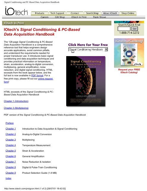
IOtech's <strong>Signal</strong> <strong>Conditioning</strong> & <strong>PC</strong>-<strong>Based</strong><br />
<strong>Data</strong> <strong>Acquisition</strong> H<strong>and</strong>book<br />
The 128-page <strong>Signal</strong> <strong>Conditioning</strong> & <strong>PC</strong>-<strong>Based</strong><br />
<strong>Data</strong> <strong>Acquisition</strong> H<strong>and</strong>book is a comprehensive<br />
reference tool that helps engineers design<br />
accurate applications, avoid common pitfalls,<br />
<strong>and</strong> underst<strong>and</strong> the requirements needed for<br />
proper transducer use. It introduces basic signal<br />
conditioning <strong>and</strong> data acquisition techniques <strong>and</strong><br />
provides practical information on temperature,<br />
strain, acceleration, analog-to-digital conversion,<br />
multiplexing, general amplification, noise<br />
reduction, <strong>and</strong> digital signal conditioning. HTML<br />
excerpts from the book appear below, <strong>and</strong> the<br />
full text is now available in PDF format. For a<br />
free print copy, please fill out our online request<br />
form!<br />
HTML excerpts of the <strong>Signal</strong> <strong>Conditioning</strong> & <strong>PC</strong>-<br />
<strong>Based</strong> <strong>Data</strong> <strong>Acquisition</strong> H<strong>and</strong>book<br />
Chapter 1 (Introduction)<br />
Chapter 3 (Multiplexing)<br />
PDF version of the <strong>Signal</strong> <strong>Conditioning</strong> & <strong>PC</strong>-<strong>Based</strong> <strong>Data</strong> <strong>Acquisition</strong> H<strong>and</strong>book<br />
Preface<br />
Chapter 1 Introduction to <strong>Data</strong> <strong>Acquisition</strong> & <strong>Signal</strong> <strong>Conditioning</strong><br />
Chapter 2 Analog-to-Digital Conversion<br />
Chapter 3 Multiplexing<br />
Chapter 4 Temperature Measurement<br />
Chapter 5 Strain & Acceleration<br />
Chapter 6 General Amplification<br />
Chapter 7 Noise Reduction & Isolation<br />
Chapter 8 Digital & Pulse-Train <strong>Conditioning</strong><br />
Chapter 9 Product Selection Guide (1.8 MB)<br />
Index<br />
http://www.iotech.com/prsigcon.html (1 of 2) [28/07/01 18:42:02]<br />
Request your FREE<br />
IOtech Catalog!
<strong>Signal</strong> <strong>Conditioning</strong> <strong>and</strong> <strong>PC</strong>-<strong>Based</strong> <strong>Data</strong> <strong>Acquisition</strong> H<strong>and</strong>book<br />
Request your copy of the <strong>Signal</strong> <strong>Conditioning</strong> H<strong>and</strong>book today!<br />
[ HOME | PRODUCTS | TECH SUPPORT | CONTACT | SEARCH/MAP | ABOUT IOTECH | SHOP ONLINE ]<br />
http://www.iotech.com/prsigcon.html (2 of 2) [28/07/01 18:42:02]<br />
® Copyright 2000, IOtech Inc.<br />
Privacy Policy
Preface <strong>Signal</strong> <strong>Conditioning</strong> H<strong>and</strong>book<br />
Preface<br />
Any industry that performs testing or monitoring has an array of transducers specifically<br />
designed for its particular measurement requirements. The intent of this h<strong>and</strong>book is to<br />
introduce the reader to the most commonly used transducer interfaces <strong>and</strong> to provide practical<br />
information for dealing with the most frequently encountered transducers <strong>and</strong> their<br />
associated signals.<br />
Transducers are available for measuring many physical quantities, such as temperature,<br />
pressure, strain, vibration, sound, humidity, flow, level, velocity, charge, pH, <strong>and</strong> chemical<br />
composition, among others. In most cases, the transducer manufacturer provides application<br />
notes on the transducer’s use <strong>and</strong> principles of operation. The main questions to<br />
consider when selecting a transducer are:<br />
• What are the electrical characteristics (amplitude, frequency, source impedance) of<br />
the transducer’s output?<br />
• What kind of power supply/excitation is required?<br />
• What is the transducer’s specified accuracy?<br />
• Over what range of amplitude <strong>and</strong> frequency are the measurements accurate?<br />
• How is the transducer calibrated?<br />
• How can transducer accuracy <strong>and</strong> calibration be verified?<br />
• In what environment (temperature, humidity, vibration, pressure) is the transducer<br />
able to operate?<br />
It is generally unwise to view a transducer as a black box that provides a specified output<br />
for a certain input. Knowing how a transducer works is imperative to making reliable<br />
measurements.<br />
i
Chapter 1 Introduction<br />
Chapter 1<br />
Introduction<br />
1
Chapter 1 Introduction<br />
This h<strong>and</strong>book is intended for newcomers to the field of data acquisition <strong>and</strong> signal<br />
conditioning. Emphasis is given to general discussions of ADC measurement <strong>and</strong> the<br />
signal conditioning requirements of selected transducer types. For more detailed descriptions<br />
of the signal conditioning schemes discussed, contact IOtech for Applications<br />
Notes <strong>and</strong> Product Specification Sheets. Additional information on IOtech products<br />
is available in Chapter 9, a product selection guide.<br />
Most measurements begin with a transducer, a device that converts a measurable physical<br />
quality, such as temperature, strain, or acceleration, to an electrical signal. Transducers<br />
are available for a wide range of measurements, <strong>and</strong> come in a variety of shapes,<br />
sizes, <strong>and</strong> specifications. This book is intended to serve as a primer for making measurements<br />
by interfacing transducers to a computer using signal conditioning.<br />
Transducer<br />
<strong>Signal</strong><br />
<strong>Conditioning</strong><br />
ADC<br />
Computer<br />
2<br />
<strong>Signal</strong> conditioning converts a<br />
transducer’s signal so that an analogto-digital<br />
converter (ADC) can measure<br />
the signal. <strong>Signal</strong> conditioning<br />
can include amplification, filtering,<br />
differential applications, isolation, simultaneous<br />
sample <strong>and</strong> hold (SS&H),<br />
current-to-voltage conversion, voltage-to-frequency<br />
conversion, linearization<br />
<strong>and</strong> more. <strong>Signal</strong> conditioning<br />
also includes excitation or bias for<br />
transducers that require it.<br />
Fig. 1.01: Generic signal-conditioning scheme Figure 1.01 depicts a generic data acquisition<br />
signal-conditioning configuration.<br />
The transducer is connected to the input of the signal conditioning electronics.<br />
The output of the signal conditioning is connected to an ADC input. The ADC converts<br />
the analog voltage to a digital signal, which is transferred to the computer for<br />
processing, graphing, <strong>and</strong> storage.<br />
Analog-to-Digital Conversion. Chapter 2 includes a discussion of the four basic ADC<br />
types, as well as issues such as accuracy, noise reduction, <strong>and</strong> discrete sampling considerations.<br />
Topics such as input <strong>and</strong> source impedance, differential voltage measurements,<br />
simultaneous sample <strong>and</strong> hold, selectable input ranges, multiplexing, <strong>and</strong> isolation<br />
are also discussed. A section on discrete sampling considerations, which covers<br />
aliasing, windowing, fast Fourier transforms (FFTs), st<strong>and</strong>ard Fourier transforms, <strong>and</strong><br />
digital filtering, is also included.
Chapter 1 Introduction<br />
Multiplexing. Chapter 3 includes a discussion on multiplexing, current measurements,<br />
<strong>and</strong> the associated issues such as simultaneous sample <strong>and</strong> hold, input buffering, <strong>and</strong><br />
methods of range <strong>and</strong> gain selection.<br />
<strong>Signal</strong> <strong>Conditioning</strong> by Chapter. <strong>Signal</strong> conditioning for a wide variety of transducer types,<br />
including temperature, strain, force, torque, pressure, <strong>and</strong> acceleration, is discussed in Chapter<br />
4 through Chapter 8. The temperature measurement section in Chapter 4 describes the<br />
principles of operation, signal conditioning, linearization, <strong>and</strong> accuracy of thermocouples,<br />
RTDs, <strong>and</strong> integrated circuits (ICs).<br />
The strain gage section in Chapter 5 discusses the Wheatstone bridge, as well as the use<br />
of strain gages in quarter-bridge, half-bridge, <strong>and</strong> full-bridge configurations. The use of<br />
strain gages in load cells is described, along with excitation <strong>and</strong> signal conditioning<br />
requirements. The piezoelectric transducers (PZTs) section in Chapter 5 describes the<br />
use of these devices in voltage <strong>and</strong> charge amplification configurations <strong>and</strong> with low<strong>and</strong><br />
high-impedance transducers. The pressure transducer section covers both<br />
strain-diaphragm transducers used for quasi-static pressure measurements <strong>and</strong> PZT-based<br />
pressure transducers used in dynamic measurements.<br />
Chapter 6 begins with a brief review of general amplification. This section then<br />
describes data acquisition front ends, source impedance <strong>and</strong> multiplexing, filters,<br />
<strong>and</strong> single-ended <strong>and</strong> differential measurements. The measurement of high voltages<br />
<strong>and</strong> DC <strong>and</strong> AC currents is also discussed.<br />
Chapter 7 discusses noise reduction <strong>and</strong> isolation, including specific methods of<br />
isolation, such as magnetic, optical, <strong>and</strong> capacitive.<br />
This h<strong>and</strong>book also describes digital signal conditioning in Chapter 8, including speed<br />
<strong>and</strong> timing issues. Also, covered in this chapter are frequency measurements, pulse<br />
counting, <strong>and</strong> pulse timing. The frequency of a signal can be measured using two<br />
methods: conversion to a voltage that is read by an ADC, or gated pulse counting. Both<br />
methods are described, as is the use of counters for timing applications.<br />
Chapter 9, IOtech’s Product Selection Guide, features <strong>PC</strong>-based data acquisition systems,<br />
signal conditioning options, <strong>and</strong> temperature measurement instruments.<br />
3
Chapter 1 Introduction<br />
4
Chapter 2 Analog-to-Digital Conversion<br />
Chapter 2<br />
Analog-to-Digital Conversion....<br />
5
Chapter 2 Analog-to-Digital Conversion<br />
This chapter examines general considerations for analog-to-digital converter (ADC) measurements.<br />
Discussed are the four basic ADC types, providing a general description of<br />
each while comparing their speed <strong>and</strong> resolution. Issues such as calibration, linearity,<br />
missing codes, <strong>and</strong> noise are discussed, as are their effects on ADC accuracy.<br />
This chapter also includes information on simultaneous sample <strong>and</strong> hold (SS&H) <strong>and</strong><br />
selectable input ranges. Finally, this chapter contains a section on discrete sampling,<br />
which includes Fourier theory, aliasing, windowing, fast Fourier transforms (FFTs), st<strong>and</strong>ard<br />
Fourier transforms, <strong>and</strong> digital filtering.<br />
ADC Types<br />
An ADC converts an analog voltage to a digital number. The digital number represents the<br />
input voltage in discrete steps with finite resolution. ADC resolution is determined by the<br />
number of bits that represent the digital number. An n-bit ADC has a resolution of 1 part in<br />
2 n . For example, a 12-bit ADC has a resolution of 1 part in 4096 (2 12 =4,096). Twelve-bit<br />
ADC resolution corresponds to 2.44 mV for a 10V range. Similarly, a 16-bit ADC’s resolution<br />
is 1 part in 65,536 (2 16 =65,536), which corresponds to 0.153 mV for a 10V range.<br />
Many different types of analog-to-digital converters are available. Differing ADC types<br />
offer varying resolution, accuracy, <strong>and</strong> speed specifications. The most popular ADC<br />
types are the parallel (flash) converter, the successive approximation ADC, the voltageto-frequency<br />
ADC, <strong>and</strong> the integrating ADC. Descriptions of each follow.<br />
Vref<br />
R/2<br />
R<br />
R<br />
R<br />
R/2<br />
Vinput<br />
+<br />
–<br />
+<br />
–<br />
+<br />
–<br />
+<br />
–<br />
Comparators<br />
Encoder<br />
Binary<br />
output<br />
Fig. 2.01: 2-bit parallel converter<br />
Flash converters are very fast (up to<br />
500 MHz) because the bits are determined<br />
in parallel. This method requires a large number of comparators, thereby<br />
limiting the resolution of most parallel converters to 8 bits (256 comparators). Flash<br />
converters are commonly found in transient digitizers <strong>and</strong> digital oscilloscopes.<br />
6<br />
Parallel (Flash) Converter<br />
The parallel converter is the simplest<br />
ADC implementation. It uses a reference<br />
voltage at the full scale of the input<br />
range <strong>and</strong> a voltage divider composed<br />
of 2n + 1 resistors in series, where<br />
n is the ADC resolution in bits. The<br />
value of the input voltage is determined<br />
by using a comparator at each<br />
of the 2n reference voltages created in<br />
the voltage divider. Figure 2.01 depicts<br />
a 2-bit parallel converter.
Chapter 2 Analog-to-Digital Conversion<br />
Successive Approximation ADC<br />
A successive approximation ADC employs<br />
a digital-to-analog converter<br />
(DAC) <strong>and</strong> a single comparator. It effectively<br />
makes a bisection or binomial<br />
search by beginning with an output of<br />
zero. It provisionally sets each bit of<br />
the DAC, beginning with the most significant<br />
bit. The search compares the<br />
output of the DAC to the voltage being<br />
measured. If setting a bit to one causes<br />
the DAC output to rise above the input<br />
voltage, that bit is set to zero. A diagram<br />
of a successive approximation<br />
ADC is shown in Figure 2.02.<br />
Successive approximation is slower than flash conversion because the comparisons must<br />
be performed in a series, <strong>and</strong> the ADC must pause at each step to set the DAC <strong>and</strong> wait<br />
for it to settle. However, conversion rates over 200 kHz are common. Successive approximation<br />
is relatively inexpensive to implement for 12- <strong>and</strong> 16-bit resolution. Consequently,<br />
they are the most commonly used ADCs, <strong>and</strong> can be found in many <strong>PC</strong>-based<br />
data acquisition products.<br />
Voltage-to-Frequency ADC<br />
Figure 2.03 depicts the voltage-to-frequency<br />
technique. Voltage-to-frequency<br />
ADCs convert an input voltage<br />
to an output pulse train with a frequency<br />
proportional to the input voltage.<br />
Output frequency is determined<br />
by counting pulses over a fixed time interval,<br />
<strong>and</strong> the voltage is inferred from<br />
the known relationship.<br />
Voltage-to-frequency conversion has a<br />
high degree of noise rejection, because<br />
the input signal is effectively integrated<br />
over the counting interval. Voltage-tofrequency<br />
conversion is commonly used<br />
to convert slow <strong>and</strong> often noisy signals.<br />
Vinput<br />
Vin Voltage-to-frequency<br />
converter<br />
Fig. 2.03: Voltage-to-frequency ADC<br />
7<br />
Comparator<br />
–<br />
+<br />
Fig. 2.02: Successive approximation ADC<br />
Digital<br />
pulse train<br />
DAC<br />
Control<br />
logic &<br />
registers<br />
Timing<br />
circuitry<br />
Pulse<br />
counter<br />
Digital<br />
outputs<br />
Digital<br />
outputs
Chapter 2 Analog-to-Digital Conversion<br />
It is also useful for remote sensing applications in noisy environments. The input voltage<br />
is converted to a frequency at the remote location, <strong>and</strong> the digital pulse train is<br />
transmitted over a pair of wires to the counter. This eliminates the noise that can be<br />
introduced in the transmission of an analog signal over a long distance.<br />
Vcapacitor<br />
I∝Vinput<br />
Ti<br />
Integration<br />
time<br />
Fixed discharge<br />
current<br />
Discharge<br />
time<br />
Vinput Ti<br />
=<br />
Vref Td<br />
Fig. 2.04: Integration <strong>and</strong> discharge of an integrating ADC<br />
Td<br />
8<br />
Integrating ADC<br />
A number of ADCs use integrating techniques,<br />
which measure the time to<br />
charge or discharge a capacitor to determine<br />
input voltage. Figure 2.04<br />
shows “Dual-slope” integration, a common<br />
integration technique. Using a<br />
current that is proportional to the input<br />
voltage, a capacitor is charged for<br />
a fixed time period. The average input<br />
voltage is determined by measuring the<br />
time required to discharge the capacitor<br />
using a constant current.<br />
Integrating the ADC input over an interval reduces the effect of noise pickup at the AC<br />
line frequency if the integration time is matched to a multiple of the AC period. For this<br />
reason, it is commonly used in precision digital multimeters <strong>and</strong> panel meters. Twentybit<br />
accuracy is not uncommon. The disadvantage is a relatively slow conversion rate (60<br />
Hz maximum, slower for ADCs that integrate over multiple line cycles).<br />
Summary of ADC Types<br />
Figure 2.05 summarizes the previously discussed ADC types <strong>and</strong> their resolution<br />
<strong>and</strong> speed ranges.<br />
ADC Type Table<br />
ADC Type Typical Typical<br />
Resolution Speed<br />
Parallel Converter 4-8 bit 100 kHz-500 MHz<br />
Successive Approximation 8-16 bit 10 kHz-1 MHz<br />
Voltage-to-Frequency 8-12 bit 1-60 Hz*<br />
Integrating 12-24 bit 1-60 Hz*<br />
* With line cycle rejection<br />
Fig. 2.05: Summary of ADC types
Chapter 2 Analog-to-Digital Conversion<br />
Accuracy<br />
Accuracy is an important consideration when selecting an ADC for use in test <strong>and</strong> measurement<br />
applications. The following section provides an in-depth discussion of accuracy considerations,<br />
pertaining to resolution, calibration, linearity, missing codes, <strong>and</strong> noise.<br />
Accuracy vs. Resolution<br />
The accuracy of a measurement is influenced by a variety of factors. If each independent<br />
error is σ , the total error is<br />
i<br />
σ total = Σ σ i 2<br />
i<br />
This calculation includes errors resulting from the transducer, noise pickup, ADC quantization,<br />
gain, offset, <strong>and</strong> other factors.<br />
ADC resolution error is termed quantization error. In an ideal ADC, any voltage in the<br />
range that corresponds to a unique digital code is represented by that code. The error in<br />
this case is half of the least significant bit (LSB) at most. For a 12-bit ADC with a 10V<br />
range, this error is 2.44 mV (0.0244%). There are three common methods of specifying<br />
a contribution to ADC error: the error in least significant bits (LSBs), the voltage error<br />
for a specified range, <strong>and</strong> the percent-of-reading error. It is important to recognize that<br />
most ADCs are not as accurate as their specified resolution, because quantization error<br />
is only one potential source of error. Nonetheless, the accuracy of a good ADC should<br />
approach its specified resolution.<br />
For more information concerning accuracy, refer to the Calibration section, which follows.<br />
For an in-depth discussion of errors arising in particular transducers, refer to<br />
Chapters 3 through 8.<br />
Figure 2.06 illustrates common error types encountered when using a 3-bit ADC. If the<br />
manufacturer provides calibration procedures, offset <strong>and</strong> gain errors can usually be reduced<br />
to negligible levels, as discussed below. However, errors in linearity <strong>and</strong> missing<br />
codes will contribute to the overall error.<br />
Calibration<br />
There are several common methods for calibrating an ADC. In hardware calibration,<br />
the offset <strong>and</strong> gain of the instrumentation amplifier that serves as the ADC front end is<br />
adjusted with trim pots. (The gain of the ADC can also be adjusted by changing the<br />
reference voltage.) In hardware/software calibration, digital-to-analog converters that<br />
null the offset <strong>and</strong> set the full scale voltages are programmed via software. In software<br />
calibration, there is no hardware adjustment. Calibration correction factors are stored<br />
in the nonvolatile memory of the data acquisition system or in the computer <strong>and</strong> used<br />
to convert the reading from the ADC.<br />
9
Chapter 2 Analog-to-Digital Conversion<br />
ADC Output<br />
Ideal<br />
7<br />
6<br />
5<br />
4<br />
3<br />
2<br />
1<br />
0<br />
0 2 4 6 8 10<br />
Input volts<br />
ADC Output<br />
Missing code<br />
7<br />
6<br />
5<br />
4<br />
3<br />
2<br />
1<br />
ADC Output<br />
Gain error<br />
7<br />
0<br />
0 2 4 6 8 10<br />
Input volts<br />
6<br />
5<br />
4<br />
3<br />
2<br />
1<br />
0<br />
0 2 4 6 8 10<br />
Input volts<br />
ADC Output<br />
Even if an ADC is calibrated at the factory, it will need to be calibrated again after a period<br />
of time (typically six months to a year, but possibly more frequently for ADCs of greater<br />
resolution than 16 bits). Variations in the operating temperature can also affect instrument<br />
calibration. Calibration procedures vary but usually require either a known reference source<br />
or a meter of greater accuracy than the device being calibrated. Typically, offset is set via a<br />
0V input, <strong>and</strong> gain is set via a full-scale input.<br />
In many measurements, the voltage is not the physical quantity under test. Consequently,<br />
it may be preferable to calibrate the complete measurement system rather than its individual<br />
parts. For example, consider a load cell for which the manufacturer specifies the<br />
output for a given load <strong>and</strong> excitation voltage. One could calibrate the ADC <strong>and</strong> combine<br />
this with the manufacturer’s specification <strong>and</strong> a measurement of the excitation voltage;<br />
however, this technique is open to error. Specifically, three distinct error sources are possible<br />
in this technique: error in the ADC calibration, error in the manufacturer’s specifications,<br />
<strong>and</strong> error in the measurement of the excitation voltage. To circumvent these error<br />
sources, one can calibrate the measurement system using known loads <strong>and</strong> obtain a direct<br />
relationship between load <strong>and</strong> ADC output.<br />
10<br />
Offset error<br />
7<br />
6<br />
5<br />
4<br />
3<br />
2<br />
1<br />
ADC Output<br />
Linearity error<br />
7<br />
0<br />
0 2 4 6 8 10<br />
Input volts<br />
6<br />
5<br />
4<br />
3<br />
2<br />
1<br />
0<br />
0 2 4 6 8 10<br />
Input volts<br />
Fig. 2.06: Common ADC error sources. The straight line is ideal output from an ADC with infinite-bit<br />
resolution. The step function shows the indicated error for a 3-bit ADC.
Chapter 2 Analog-to-Digital Conversion<br />
Linearity<br />
If input voltage <strong>and</strong> ADC output deviate from the diagonal lines in Figure 2.06 more than<br />
the ideal step function, the result is ADC error that is nearly impossible to eliminate by<br />
calibration. This type of ADC error is referred to as nonlinearity error. If nonlinearity is<br />
present in a calibrated ADC, the error is often largest near the middle of the input range, as<br />
shown in Figure 2.06. The nonlinearity in a good ADC should be 1 LSB or less.<br />
Missing Codes<br />
Some ADCs have missing codes. In Figure 2.06, the ADC does not provide an output of<br />
four for any input voltage. This error can result in a significant loss in resolution <strong>and</strong><br />
accuracy. A quality ADC should have no missing codes.<br />
Noise<br />
Many users are surprised by noise encountered when measuring millivolt signals or<br />
attempting accurate measurements on larger signals. Investing in an accurate ADC<br />
is only the first step in accurately measuring analog input signals. Controlling noise<br />
is imperative.<br />
Many ADCs reside on cards that plug into a <strong>PC</strong> expansion bus, where electrical noise can<br />
present serious problems. Expansion bus noise often far exceeds the ADC’s sensitivity<br />
resulting in significant loss of measurement accuracy. Placing the ADC outside the <strong>PC</strong> is<br />
often a better solution. An ADC in an external enclosure can communicate with the<br />
computer over an IEEE 488 bus, serial port, or parallel port. If an application requires<br />
placement of the ADC within the computer, the noise level should be tested by connecting<br />
the ADC input to signal common <strong>and</strong> observing deviations in ADC output. (Connecting<br />
the ADC input to signal common isolates the cause of the noise to the circuit<br />
card. More careful diagnostics are necessary when using an external voltage source because<br />
noise can arise from the external source <strong>and</strong> from the input leads.)<br />
Noise Reduction <strong>and</strong> Measurement Accuracy<br />
One technique for reducing noise <strong>and</strong> ensuring measurement accuracy is with isolation,<br />
which also eliminates ground loops. Ground loops occur when two or more devices in<br />
a system, such as a measurement instrument <strong>and</strong> a transducer, are connected to ground<br />
at different physical locations. Slight differences in the actual potential of each ground<br />
results in a current flow from one device to the other. This current, which often flows<br />
through the low lead of a pair of measurement wires, generates a voltage drop which can<br />
directly lead to measurement inaccuracies <strong>and</strong> noise. If at least one device is isolated,<br />
such as the measurement device, then there is no path for the current flow, <strong>and</strong> thereby<br />
no contribution to noise or inaccuracy.<br />
11
Chapter 2 Analog-to-Digital Conversion<br />
Protection<br />
Many data acquisition systems utilize solid-state multiplexing circuitry in order to<br />
very quickly scan multiple input channels. These solid-state multiplexers are among<br />
the most susceptible circuitry to overload voltages, which can commonly occur in a<br />
system. Typically, multiplexers can only accept up to 20 or 30 volts before damage<br />
occurs. Other solid-state devices in a measurement system include input amplifiers<br />
<strong>and</strong> bias sources, both of which are also susceptible to damage from over voltage.<br />
Isolation is one of a number of techniques used to protect sensitive solid-state circuitry<br />
in a data acquisition system.<br />
Although isolation does not protect against excessive normal-mode input voltage (voltage<br />
across a pair of inputs), it does protect against excessive common-mode voltage. It<br />
accomplishes this by eliminating the potentially large current that would otherwise flow<br />
from the signal source to the data acquisition system, as a result of the common mode<br />
voltage. By eliminating this current flow, the possibility of damage is eliminated.<br />
High common-mode voltage measurements<br />
It is often necessary to measure a small voltage which is residing on another, much larger<br />
voltage. For example, if a thermocouple is mounted to one terminal of a battery, then<br />
the measurement device must be capable of measuring the microvolt output of the thermocouple<br />
while rejecting the battery voltage. If the common-mode voltage is less than<br />
10-15V, a differential measurement via an instrumentation amplifier will read the thermocouple<br />
voltage while ignoring the battery voltage. If the common-mode voltage is<br />
higher than 10-15V, an isolation method is generally required.<br />
Vinput<br />
–<br />
+<br />
Photo<br />
diode<br />
LED<br />
Input<br />
ground<br />
LED<br />
Photo<br />
diode<br />
Fig. 2.07: Optically-coupled isolation amplifier<br />
–<br />
+<br />
R<br />
Output<br />
ground<br />
Voutput<br />
12<br />
There are several isolation methods<br />
with the common characteristic of a<br />
high common-mode voltage from input<br />
to output. Each channel can have<br />
an isolation amplifier, or, a group of<br />
channels that are not isolated from<br />
each other can be multiplexed <strong>and</strong><br />
digitized by an analog-to-digital converter<br />
before the digital data is isolated<br />
from the remainder of the system.<br />
Actual isolation barriers can be optical,<br />
magnetic, or capacitive. The most<br />
common are optical schemes in which
Chapter 2 Analog-to-Digital Conversion<br />
infrared emission from an LED is detected by a photodiode on the opposite side of a<br />
quartz barrier. Figure 2.07 illustrates an optically-coupled isolation amplifier. Optocouplers<br />
can be used to transmit pulse trains in which frequency or pulse width vary with<br />
analog signal magnitude or which contain numerical data in serial pulse trains. It is<br />
even possible to transmit analog information by varying LED current as in Figure 2.07.<br />
Magnetic barriers using transformers <strong>and</strong> capacitive barriers are generally internal <strong>and</strong><br />
used in monolithic or hybrid isolation amplifiers.<br />
Frequency Coupled Isolation. In frequency coupled isolation, a high frequency carrier<br />
signal is inductively or capacitively coupled across the isolation barrier. The signal is<br />
modulated on the input side <strong>and</strong> demodulated on the output side to reproduce the<br />
original input signal.<br />
Isolated ADC. When using an isolated ADC, the ADC <strong>and</strong> accompanying signal conditioning<br />
are floated. The input signal is converted to a digital signal by the ADC <strong>and</strong> the<br />
interface for transferring the digital code is digitally isolated. See Chapter 6 for a detailed<br />
discussion.<br />
Discrete Sampling Considerations<br />
The Nyquist sampling theorem says that if a signal only contains frequencies less than<br />
cutoff frequency f , all the information in the signal can be captured by sampling at 2f .<br />
c c<br />
The upshot of this is that capturing a signal with maximum frequency component fmax requires sampling at a rate of at least 2f . In practice, for working in the frequency<br />
max<br />
domain, it is best to set the sampling rate between five <strong>and</strong> ten times the signal’s highest<br />
frequency component. However, for viewing waveforms in the time domain, it is not<br />
uncommon to sample 10 times the frequency of interest. One reason is to retain accuracy<br />
at the signal’s higher frequency components.<br />
Aliasing<br />
Aliasing can also be seen in the time domain. Figure 2.09 shows a 1-kHz sine wave<br />
sampled at 800 Hz. The apparent frequency of the sine wave is much too low. Figure<br />
2.08 shows the result of sampling the same 1-kHz sine wave at 5 kHz. The sampled wave<br />
appears to have the correct frequency.<br />
Aliasing is the main reason to sample at a rate higher than the Nyquist frequency.<br />
Aliasing—the generation of false, low-frequency signals—occurs when an ADC’s sampling<br />
rate is too low. Input signals are seldom b<strong>and</strong>width limited with zero amplitude<br />
higher than f max . A signal with frequency components higher than one-half the sampling<br />
frequency will cause the amplitude to appear below one-half the sampling frequency<br />
in the Fourier transform. This is called aliasing, <strong>and</strong> it can cause inaccuracies in<br />
sampled signal <strong>and</strong> also in the Fourier transform.<br />
13
Chapter 2 Analog-to-Digital Conversion<br />
1<br />
0.8<br />
0.6<br />
0.4<br />
0.2<br />
0<br />
-0.2<br />
-0.4<br />
-0.6<br />
-0.8<br />
-1<br />
0 100 200 300 400 500 600<br />
Fig. 2.08: When sampled at just over 2 times the<br />
frequency of the sine wave, the frequency content of<br />
the signal is retained<br />
Aliasing is illustrated in Figure 2.10, which shows a square wave’s Fourier transform.<br />
For the purpose of illustration, assume that the experiment has been designed to provide<br />
only frequencies of under 2 kHz. Ideally, a Fourier transform of a 500-Hz square<br />
wave contains one peak at 500 Hz, <strong>and</strong> another at 1500 Hz, which is one third the<br />
height of the first peak. In Figure 2.10, however, higher frequency peaks are aliased<br />
into the Fourier transform’s low-frequency range.<br />
Volts<br />
Actual Sine Wave Sampled at about 2 times fundamental<br />
1<br />
0.9<br />
0.8<br />
0.7<br />
0.6<br />
0.5<br />
0.4<br />
0.3<br />
0.2<br />
0.1<br />
0<br />
0 500 1000 1500 2000<br />
Frequency [Hz]<br />
Fig. 2.10: Fourier transform of a 500-Hz square wave<br />
sampled at 4 kHz with no filtering<br />
14<br />
1<br />
0.8<br />
0.6<br />
0.4<br />
0.2<br />
0<br />
-0.2<br />
-0.4<br />
-0.6<br />
-0.8<br />
-1<br />
0 100 200 300 400 500 600<br />
Actual Sine Wave Sampled at about 1/2 times fundamental<br />
Fig. 2.09: When sampling too slowly, the acquired<br />
waveform erroneously represents the real sine wave<br />
The use of a low-pass filter at 2 kHz, as<br />
shown in Figure 2.11, removes most<br />
of the aliased peaks. Low-pass filters<br />
used for this purpose are often called<br />
“anti-aliasing” filters.<br />
When the sampling rate is increased to<br />
four times the highest frequency of interest,<br />
the Fourier transform in the range<br />
of interest looks even better. Although<br />
a small peak remains at 1,000 Hz, it is<br />
probably the result of an imperfect<br />
square wave rather than an effect of aliasing.<br />
See Figure 2.12.
Chapter 2 Analog-to-Digital Conversion<br />
Volts<br />
1.4<br />
1.2<br />
1<br />
0.8<br />
0.6<br />
0.4<br />
0.2<br />
0<br />
0 500 1000<br />
Frequency [Hz]<br />
1500 2000<br />
Fig. 2.11: Fourier transform of 500-Hz square<br />
wave sampled at a 4 kHz with low-pass filter cutoff<br />
at 2 kHz<br />
Windowing<br />
Windowing is the multiplication of the input signal with a weighting function to<br />
reduce spurious oscillations in a Fourier transform. Real measurements are performed<br />
over finite time intervals. In contrast, Fourier transforms are defined over<br />
infinite time intervals. As such, the Fourier transform of sampled data is an approximation.<br />
Consequently, the resolution of the Fourier transform is limited to<br />
roughly 1/T, where T is the finite time interval over which the measurement was<br />
made. Fourier transform resolution can only be improved by sampling for a longer<br />
interval.<br />
Using a finite time interval also causes spurious oscillations in the Fourier transform.<br />
From a mathematical viewpoint, spurious oscillations are caused by the signal<br />
being instantaneously turned on at the beginning of the measurement <strong>and</strong> then<br />
suddenly turned off at the end of the measurement. Figure 2.13 illustrates an example<br />
of spurious oscillations.<br />
Implementing window functions can help minimize spurious oscillations of a signal.<br />
Multiplying the sampled data by a window function that rises gradually from zero decreases<br />
the spurious oscillations at the expense of a slight loss in triggering resolution.<br />
There are many possible window functions, all of which involve trade-offs between<br />
amplitude estimation <strong>and</strong> frequency resolution.<br />
15<br />
Volts<br />
1.6<br />
1.4<br />
1.2<br />
1<br />
0.8<br />
0.6<br />
0.4<br />
0.2<br />
0<br />
0 500 1000<br />
Frequency [Hz]<br />
1500 2000<br />
Fig. 2.12: Fourier transform of 500-Hz square<br />
wave sampled at 8 kHz with low-pass filter cutoff<br />
at 2 kHz
Chapter 2 Analog-to-Digital Conversion<br />
Amplitude<br />
Fast Fourier Transforms<br />
The fast Fourier transform (FFT) is so common today that “FFT” has become an imprecise<br />
synonym for Fourier transforms in general. The FFT is a digital algorithm for computing<br />
Fourier transforms of data discretely sampled at a constant interval. The FFT’s<br />
simplest implementation requires 2 n samples. Other implementations accept other special<br />
numbers of samples. If the data set to be transformed has a different number of<br />
samples than required by the FFT algorithm, the data is often padded with zeros to<br />
achieve the required number. This leads to inaccuracies, but they are often tolerable.<br />
2<br />
1.5<br />
1<br />
0.5<br />
0<br />
-0.5<br />
-1<br />
-1.5<br />
-2<br />
1.2<br />
1<br />
0.8<br />
0.6<br />
0.4<br />
0.2<br />
0<br />
450 460 470 480 490 500 510 520 530 540 550<br />
Frequency [Hz]<br />
Fourier transform of a sine wave using a window function<br />
Fourier transform of a sine wave with no window function<br />
Fig. 2.13: A Fourier transform with window<br />
function <strong>and</strong> without window function<br />
Fig. 2.15: When multiplied by a window function,<br />
the frequency information is preserved while<br />
minimizing the affect of irregularities at the<br />
beginning <strong>and</strong> end of the sample segment<br />
16<br />
Fig. 2.14: Without window function, abrupt<br />
beginning <strong>and</strong> end points of waveform produce<br />
erroneous frequency information<br />
2.5<br />
2<br />
1.5<br />
1<br />
0.5<br />
0<br />
Hamming Hanning Blackman<br />
Fig. 2.16: Three common window types
Chapter 2 Analog-to-Digital Conversion<br />
St<strong>and</strong>ard Fourier Transforms<br />
A st<strong>and</strong>ard Fourier transform (SFT) can be used in applications where the number of<br />
samples cannot be arranged to fall on one of the special numbers required by an FFT.<br />
The SFT is also useful for applications that cannot tolerate the inaccuracies introduced<br />
by padding with zeros, a h<strong>and</strong>icap of the FFT.<br />
The SFT is also suited to applications where the data is not sampled at evenly spaced<br />
intervals or where sample points are missing. Finally, the SFT can be used to provide<br />
more closely spaced points in the frequency domain than can be obtained with an FFT.<br />
(In an FFT, adjacent points are separated by half the sampling frequency. Points arbitrarily<br />
close in frequency can be obtained using an SFT.)<br />
There are many st<strong>and</strong>ard numerical integration techniques available for computing SFTs<br />
from sampled data. Whichever technique is selected for the problem at h<strong>and</strong>, it will<br />
probably be much slower than an FFT of a similar number of points. This is becoming<br />
less of an issue, however, as the speed of modern computers increases.<br />
Digital Filtering<br />
Digital filtering is accomplished in<br />
three steps. First, the signal must be<br />
subjected to a Fourier transform.<br />
Then, the signal’s amplitude in the<br />
frequency domain must be multiplied<br />
by the desired frequency response. Finally,<br />
the transferred signal must be<br />
inverse Fourier transformed back into<br />
the time domain. Figure 2.17 shows<br />
the effect of digital filtering on the<br />
noisy signal. Note that the solid line<br />
represents the unfiltered signal, while<br />
the two dashed lines represent different<br />
digital filters.<br />
Volts<br />
Digital filtering is advantageous because the filter itself can be easily tailored to any<br />
frequency response without introducing phase error. However, one disadvantage of<br />
digital filtering is that it cannot be used for anti-aliasing.<br />
Analog Filtering<br />
In contrast to digital filtering, analog filtering can be used for anti-aliasing, but it is more<br />
difficult to change the frequency response curves, since all analog filters introduce some<br />
element of phase error.<br />
17<br />
1.546<br />
1.544<br />
1.542<br />
1.54<br />
1.538<br />
1.536<br />
1.534<br />
0 0.05 0.1 0.15 0.2 0.25<br />
Time [seconds]<br />
Unfiltered signal<br />
50Hz low-pass digital filter<br />
5Hz low-pass digital filter<br />
Fig. 2.17: The effect of digital filtering on the noisy signal
Chapter 2 Analog-to-Digital Conversion<br />
Sampling Hints<br />
There are several important “sampling hints” to observe when designing an application.<br />
These hints are not absolutes nor do they guarantee optimal results. However, they do<br />
provide a useful starting point for planning frequency analysis of a physical process.<br />
These sampling hints include:<br />
• A Fourier transform’s highest meaningful frequency is one-half of the<br />
sampling frequency<br />
• The sampling rate should be at least three to five times the highest frequency<br />
of interest<br />
• An anti-aliasing low-pass filter is typically required; the cutoff frequency should<br />
be close to the signal’s highest frequency of interest<br />
• Digital filtering can be used to smooth the data or to remove noise in a specified<br />
range after acquisition; however, aliasing can only be prevented with an<br />
analog low-pass filter<br />
• If the phase relationship between multiple signals is important, a simultaneous<br />
sample <strong>and</strong> hold circuit should be used (see multiplexing in Chapter 3)<br />
• Fourier transform resolution is inversely proportional to measurement time;<br />
acquiring data over a longer period of time results in narrower peaks in the<br />
Fourier transform.<br />
18
Chapter 3 Multiplexing<br />
Chapter 3<br />
Multiplexing<br />
19
Chapter 3 Multiplexing<br />
Multiplexing<br />
A multiplexer is a switch that allows a<br />
single ADC to measure many input<br />
channels. This switch can be implemented<br />
via relays or solid-state switches.<br />
A relay is a mechanical switch, so rates<br />
are relatively slow (less than 1 kHz for<br />
reed relays, which are the fastest type),<br />
but large voltages <strong>and</strong> high isolation<br />
(several kV) can be achieved. The current<br />
capacity of a relay is determined by<br />
its size <strong>and</strong> contact type. Currents of 3A<br />
are typical in relays used in laboratory<br />
instruments. Much larger currents can<br />
be switched with the larger relays common<br />
in industrial applications.<br />
Analog<br />
inputs<br />
Solid-state switches are much faster than relays, <strong>and</strong> speeds of several MHz are common.<br />
However, these small devices are easily destroyed by voltages larger than 25V,<br />
<strong>and</strong> they are a poor choice for isolated applications. Solid-state switches typically support<br />
currents less than 1 mA.<br />
A multiplexing scheme such as that shown in Figure 3.01 eliminates the high cost of<br />
having multiple ADCs. A programmable gain amplifier (PGA) allows each channel to<br />
have a different gain <strong>and</strong> input range. Multiplexing reduces the rate at which data can<br />
be acquired from an individual channel, because multiple channels are scanned sequentially.<br />
For example, an ADC that can sample a single channel at 100 kHz is limited<br />
to a 12.5-kHz per-channel sampling rate when sampling eight channels.<br />
IOtech’s 100-kHz <strong>and</strong> 1-MHz data acquisition systems are examples of systems that use<br />
software selectable channel <strong>and</strong> gain sequencing. IOtech’s 100-kHz systems provide a<br />
512-location scan sequencer that allows you to select, via software, each channel <strong>and</strong> its<br />
associated input amplifier gain for both the built-in channels <strong>and</strong> the expansion channels.<br />
The sequencer circuitry circumvents a major limitation encountered with many plug-in<br />
data acquisition boards—a drastic reduction in the scan rate for expansion channels. All<br />
channels are scanned, including expansion channels, at 100 kHz (10 μs/channel). Digital<br />
inputs can also be scanned using the same scan sequence employed for analog inputs,<br />
enabling the time correlation of acquired digital data to acquired analog data. These products<br />
permit each scan group, containing up to 512 channel/gain combinations, to be repeated<br />
immediately or at programmable intervals of up to 12 hours. Within each scan<br />
group, consecutive channels are measured at a fixed 10 μs/channel rate. Figure 3.02 illustrates<br />
a 512-location scan sequencer operating in a 100-kHz data acquisition system.<br />
20<br />
Mux<br />
Mux<br />
control lines<br />
PGA<br />
Gain<br />
control lines<br />
ADC<br />
Fig. 3.01: The multiplexer (Mux) is a fast switch that<br />
directs different input signals to the ADC for digitizing
Chapter 3 Multiplexing<br />
Scan group<br />
Programmable<br />
Constant<br />
scan rate<br />
All channels within a scan group are<br />
measured at a fixed scan rate<br />
Channel #2 #4 #7 #2 D #18 #19 #16<br />
x1 x8 x8 x2 x100 x10 x1000<br />
Uni Uni Bi Uni Bi Bi Uni<br />
1<br />
Gain2 Unipolar or Bipolar3 4 5<br />
1. Unipolar or bipolar operation can be programmed for each channel dynamically by the sequencer<br />
2. Gain can be programmed for each channel dynamically by the sequencer<br />
3. Channels can be sampled dynamically by the sequencer<br />
4. Expansion channels are sampled at the same rate as on-board channels<br />
Fig. 3.02: 512-location scan sequencer example<br />
Unfortunately, multiplexing may introduce problems. A high source impedance can combine<br />
with stray capacitance to cause settling problems <strong>and</strong> crosstalk between channels. Multiplexer<br />
impedance can also lead to signal degradation. A solid state multiplexer can have an<br />
impedance of tens of Ohms, whereas a relay typically has a resistance of less than 0.01 Ohm.<br />
Sequence vs. Software Selectable Ranges<br />
Most data acquisition system implementations permit different input ranges, although<br />
the manner in which they do so varies considerably. Some data acquisition systems<br />
allow the input range to be switched or jumper selected on the circuit board. Others<br />
provide software selectable gain; this is more convenient, but a distinction should be<br />
made between data acquisition systems whose channels must all have the same gain,<br />
<strong>and</strong> systems that allow you to sequentially select the input range of each channel. It is<br />
often advantageous to have different input ranges on different channels, especially when<br />
measuring signals from different transducers. Thermocouples <strong>and</strong> strain gages require<br />
input ranges of tens of millivolts, while other transducers might output several volts.<br />
A data acquisition system with a software selectable range can be used to measure different<br />
ranges on different channels at a relatively slow rate by issuing a software comm<strong>and</strong><br />
to change the gain between samples.<br />
There are two problems with this technique. First, it is slow; issuing a software<br />
comm<strong>and</strong> to change the gain of a PGA can take tens or hundreds of milliseconds,<br />
lowering the sample rate to several Hz. Second, the speed of this sequence is often<br />
indeterminate, due to variants in the <strong>PC</strong> instruction cycle times. So cycling through<br />
it continuously will give samples with an uneven (<strong>and</strong> unknown) spacing in time.<br />
This complicates time-series analysis <strong>and</strong> makes FFT analysis impossible since the<br />
FFT requires evenly spaced samples.<br />
21<br />
t<br />
t
Chapter 3 Multiplexing<br />
Analog<br />
inputs<br />
Expansion<br />
channel addressing<br />
Expansion<br />
gain addressing<br />
16<br />
to<br />
1<br />
Mux<br />
4<br />
2<br />
4<br />
x1, x2, x4, & x8<br />
PGA<br />
To data<br />
acquisition<br />
system<br />
Fig. 3.03: Multiplexer scheme with sequence selectable gain<br />
2<br />
Hardware<br />
sequencer<br />
CLK<br />
Triggering<br />
circuitry<br />
22<br />
As discussed earlier, a better implementation<br />
provides a sequencer that controls<br />
the channel selection <strong>and</strong> gain.<br />
The maximum acquisition rate can be<br />
achieved with sequence-selectable<br />
ranges, whereas the acquisition rate<br />
will slow considerably with softwareselectable<br />
ranges if channels require<br />
different ranges. IOtech’s 100-kHz<br />
data acquisition systems provide a<br />
512-location scan sequencer that allows<br />
you to select each channel <strong>and</strong><br />
associated input amplifier gain at<br />
r<strong>and</strong>om. These products permit each<br />
scan group to be repeated immediately<br />
or at programmable intervals.<br />
Input Buffering<br />
The impact of source impedance <strong>and</strong> stray capacitance can be estimated via a simple<br />
formula: the time constant associated with a source impedance (R) <strong>and</strong> stray capacitance<br />
(C) is T=RC.<br />
For example, suppose you want to know the maximum tolerable input impedance<br />
for a 100-kHz multiplexer. The time between measurements on adjacent channels<br />
in the scan sequence is 10 μs. In a<br />
length of time T=RC, the voltage er-<br />
Inputs<br />
ror decays by a factor of 2.718. Re-<br />
Buffer<br />
ducing the error to 0.005% requires<br />
waiting 10T.<br />
Buffer<br />
Buffer<br />
Buffer<br />
Mux<br />
ADC<br />
PGA<br />
Fig. 3.04: Buffering signals before the multiplexer<br />
increases accuracy, especially with high-impedance<br />
sources or fast multiplexing<br />
Consequently, a fixed time of 10 μs between<br />
scans (T scan ) <strong>and</strong> an error of 0.005%<br />
would appear to require a time of T=1<br />
μs. In a typical multiplexed data acquisition<br />
system, this would yield errors due<br />
to insufficient settling time. The difference<br />
can be explained as follows. Most<br />
100-kHz converters require 2 μs (T samp )<br />
to sample the input signal. Subtracting<br />
this from the scan time results in a settling<br />
time of: T settle =T scan -T samp , T settle =8 μs.
Chapter 3 Multiplexing<br />
If we assume a typical 16-bit data acquisition system, the internal settling time<br />
(T ) may be 6 μs. The external settling time may then be computed as follows:<br />
int<br />
2 2 T =√ T -Tint , Text =5.29 μs.<br />
ext settle<br />
For a 16-bit data acquisition system with 100 picofarad of input capacitance<br />
(C in ) <strong>and</strong> a multiplexer resistance (R mux ) of 100 Ohms, the maximum external resistance<br />
is calculated as follows: R ext = (T ext /C in 1n(2 16 ))-R mux , R ext =4,670 Ohms.<br />
The above examples are simplified <strong>and</strong> do not included any effects due to multiplexer<br />
charge injection or inductive reactance in the measurement wiring. In actual practice<br />
the practical upper limit on source resistance is between 1,500 <strong>and</strong> 2,000 Ohms.<br />
Most input signals have source impedances of less than 1.5 KOhm, so such a maximum<br />
source impedance is usually not a problem. However, faster multiplexer rates require lower<br />
source impedances. For example, a 1-MHz multiplexer in a 12-bit system requires a source<br />
impedance of under 1.5 KOhm. If the source impedance exceeds this value, buffering is<br />
necessary to obtain accurate measurements. A buffer is an amplifier with high input impedance<br />
<strong>and</strong> very low output impedance. Placing a buffer on each channel between the<br />
transducer <strong>and</strong> the multiplexer eliminates inaccuracies by preventing the multiplexer’s stray<br />
capacitance from having to discharge through the impedance of the transducer. IOtech’s<br />
Wave<strong>Book</strong>, Log<strong>Book</strong>, Personal Daq, <strong>and</strong> select signal conditioning options are all highspeed<br />
devices that use this configuration. This arrangement is illustrated in Figure 3.04.<br />
Simultaneous Sample <strong>and</strong> Hold (SS&H)<br />
A multiplexed ADC measurement introduces a time skew among channels, which is intolerable<br />
in some applications. Employing simultaneous sample <strong>and</strong> hold (SS&H) on multiple<br />
channels remedies time-skew<br />
problems. Simultaneous<br />
sample <strong>and</strong> hold requires that<br />
each channel be equipped with<br />
a buffer that samples the signal<br />
at the beginning of the scan<br />
sequence. The signal at the<br />
buffer output is held at the<br />
sampled value while the multiplexer<br />
switches through all<br />
channels <strong>and</strong> the ADC digitizes<br />
the readings. In a good simultaneous<br />
sample <strong>and</strong> hold<br />
implementation, all channels<br />
are sampled within 100 ns of<br />
each other.<br />
Ch 1<br />
Ch 2<br />
Ch 3<br />
Ch 4<br />
Fig. 3.05: DBK45 4-channel, low-pass filtering with simultaneous<br />
sample <strong>and</strong> hold card block diagram<br />
23<br />
IA LPF S/H<br />
IA LPF S/H<br />
IA LPF S/H<br />
IA LPF S/H<br />
Switched bias resistors<br />
(per channel)<br />
Mux<br />
Channel address lines<br />
Sample enable<br />
To data<br />
acquisition<br />
system
Chapter 3 Multiplexing<br />
Figure 3.05 shows a common scheme for simultaneous sample <strong>and</strong> hold; this design is used<br />
on IOtech’s DBK45 simultaneous sample <strong>and</strong> hold card, an expansion option for IOtech’s<br />
100-kHz data acquisition systems. Each input signal passes through an instrumentation<br />
amplifier (IA) <strong>and</strong> into a sample <strong>and</strong> hold buffer (S/H). When the sample enable line goes<br />
high, each S/H samples its input signal <strong>and</strong> holds it while the multiplexer switches through<br />
the readings. This scheme ensures that all the samples are taken within 50 ns of each other,<br />
even with up to sixty-four DBK45s connected to a single instrument. A system configured<br />
with sixty-four DBK45s would provide 256 simultaneous channels.<br />
i<br />
R<br />
– ADC<br />
+<br />
100k Ohm<br />
Fig. 3.06: Current measurement using a shunt resistor<br />
<strong>and</strong> a differential amplifier<br />
24<br />
Current Measurements<br />
Many transducers can be configured to<br />
output a 4-20 mA current with a linear<br />
relationship to the quantity being<br />
measured. A shunt resistor converts<br />
the current to a voltage for measurement<br />
by an ADC. Figure 3.06 illustrates<br />
current measurement. If the current<br />
(I) is passed through a resistance<br />
(R), the voltage across the resistor is<br />
V=IR. Consequently, a 500 Ohm resistor<br />
is sufficient to map a 20 mA fullscale<br />
current into a 10 VFS voltage for<br />
measurement with a data acquisition<br />
system. Using a transducer configured<br />
for current output can yield high noise immunity <strong>and</strong> accuracy, particularly if there is a<br />
large distance between the data acquisition system <strong>and</strong> the transducer. Long leads pick<br />
up noise <strong>and</strong> suffer an ohmic voltage drop.<br />
The current value inferred from measuring the voltage across a shunt resistor is only as<br />
accurate as the resistor. Common resistor accuracies are 5%, 1%, 0.1%, <strong>and</strong> 0.01%.<br />
Resistors are commonly specified according to their accuracy <strong>and</strong> stability when exposed<br />
to changing temperatures. All resistors change with temperature. This phenomenon<br />
can be used to measure temperature, as discussed in Chapter 4, however, this<br />
effect is undesirable when measuring current. Many resistor manufacturers make an<br />
effort to lower the effects of changing temperatures on resistance. This specification<br />
means that the actual resistance is within the specified tolerance of the given resistance.<br />
In addition, a 0.1% resistor usually has a lower temperature coefficient <strong>and</strong><br />
better long-term stability than a resistor with lower accuracy, due to its construction<br />
technique, which is usually wire wound or metal film vs. carbon composition.
Chapter 4 Temperature Measurement<br />
Chapter 4<br />
Temperature Measurement<br />
25
Chapter 4 Temperature Measurement<br />
This chapter examines various transducers for measuring temperature: thermocouples, <strong>and</strong><br />
RTDs. It also discusses the required signal conditioning, as well as various techniques for<br />
optimizing the accuracy of your temperature measurement.<br />
+<br />
-<br />
eAB<br />
Metal A (copper)<br />
Metal B (constantan)<br />
Fig. 4.01: Illustration of a Type T thermocouple<br />
Type T<br />
26<br />
Thermocouples<br />
Thermocouples are probably the most<br />
widely used <strong>and</strong> least understood of all<br />
temperature measuring devices. Thermocouples<br />
provide a simple <strong>and</strong> efficient<br />
means of temperature measurement<br />
by generating a voltage that is a<br />
function of temperature. All electrically<br />
conducting materials produce a thermal<br />
electromotive force (emf or voltage difference)<br />
as a function of the temperature<br />
gradients within the material. This<br />
is called the Seebeck effect. The amount<br />
of the Seebeck effect depends on the<br />
chemical composition of the material<br />
used in the thermocouple.<br />
When two different materials are connected to create a TC, a voltage is generated.<br />
This voltage is the difference of the voltages generated by the two materials. In<br />
principle, a thermocouple can be made from almost any two metals. In practice,<br />
several thermocouple types have become de facto st<strong>and</strong>ards because they possess<br />
desirable qualities, such as highly predictable output voltages <strong>and</strong> large voltage-totemperature<br />
ratios. Some common thermocouple types are J, K, T, E, N28, N14, S, R,<br />
<strong>and</strong> B. Figure 4.01 depicts a Type T thermocouple. In theory, the temperature can<br />
be inferred from such a voltage by consulting st<strong>and</strong>ard tables or using linearization<br />
algorithms. In practice, this voltage cannot be directly used, because the connection<br />
of the thermocouple wires to the measurement device constitutes a thermocouple<br />
providing another thermal emf that must be compensated for; cold junction<br />
compensation can be used for this purpose.<br />
Cold Junction Compensation. Figure 4.02 shows a thermocouple that has been placed<br />
in series with a second thermocouple, which has been placed in an ice bath. This ice<br />
bath is called the reference junction. And when properly constructed, an ice bath can<br />
produce an extremely accurate 0˚C temperature. This reference junction is required<br />
because all thermocouple emf tables, as published by NIST (National Institute of St<strong>and</strong>ards<br />
<strong>and</strong> Technology), are referenced to the emf output of a thermocouple which is
Chapter 4 Temperature Measurement<br />
held at a temperature of 0.00 degrees<br />
Celsius. In figure 4.02, the chromel/<br />
copper <strong>and</strong> alumel/copper thermocouples<br />
in the ice bath have a 0.0V<br />
contribution to the voltage measured<br />
at the meter. The voltage read is entirely<br />
from the chromel/alumel thermocouple.<br />
The copper wires con-<br />
Copper<br />
+<br />
V<br />
-<br />
Copper<br />
Copper<br />
Copper<br />
Chromel<br />
+<br />
V1<br />
-<br />
Alumel<br />
nected to the copper terminals on the<br />
meter do not constitute a thermo-<br />
Volt meter<br />
couple because they are the same<br />
metal connection <strong>and</strong> both terminals<br />
are the same temperature.<br />
Ice Bath<br />
Fig. 4.02: Thermocouple circuit with ice bath<br />
Maintaining an ice bath <strong>and</strong> an additional<br />
reference thermocouple for<br />
every thermocouple probe is not practical in most systems. If we know the temperature<br />
at the point where we connect to our thermocouple wires, ( the reference junction<br />
), <strong>and</strong> if both connecting wires are at the same temperature, then the ice bath<br />
can be eliminated. In such a case, the opposing thermoelectric voltage generated by<br />
the nonzero temperature of the reference junction can simply be added to the thermocouple<br />
emf. This is cold junction compensation (CJC).<br />
CJC is an essential part of accurate thermocouple readings. CJC must be implemented<br />
in any system that has no ice-point reference junction. The technique works best if the<br />
CJC device is close to the terminal blocks that connect the external thermocouples, <strong>and</strong><br />
if there are no temperature gradients in the region containing the CJC <strong>and</strong> terminals.<br />
Thermocouple Linearization. Thermocouple voltage is proportional to, but not linearly<br />
proportional to, the temperature at the thermocouple connection. There are<br />
several techniques for thermocouple linearization. Analog techniques can provide<br />
a voltage proportional to temperature from the thermocouple input. In addition, a<br />
voltage measurement can be made with an ADC <strong>and</strong> the temperature looked up in a<br />
table, as in the above example. To speed this process, the lookup table can be stored<br />
in computer memory <strong>and</strong> the search performed with an algorithm. Thermocouple<br />
linearization can also be accomplished using a polynomial approximation to the<br />
temperature versus voltage curve. Figure 4.03 on the next page illustrates a portion<br />
of the NIST Polynomial Coefficients table for some common thermocouples.<br />
27
Chapter 4 Temperature Measurement<br />
a0 a1 a2 a3 a4 a5 a6 a7 a8 a9 Type E<br />
Nickel-10%<br />
Chromium(+) vs.<br />
Constantan(–)<br />
–100°C to 1000°C<br />
±0.5°C<br />
9th order<br />
0.104967248<br />
17189.45282<br />
–282639.0850<br />
12695339.5<br />
–448703084.6<br />
1.10866E + 10<br />
–1.76807E + 11<br />
1.71842E + 12<br />
–9.19278E + 12<br />
2.06132E + 13<br />
NIST Polynomial Coefficients<br />
Type J Type K Type R Type S<br />
Iron(+) vs.<br />
Constantan(–)<br />
0°C to 760°C<br />
±1°C<br />
5th order<br />
–0.048868252<br />
19873.14503<br />
–218614.5353<br />
11569199.78<br />
–264917531.4<br />
2018441314<br />
Nickel-10%<br />
Chromium(+) vs.<br />
Nickel–5%(–)<br />
(Aluminum Silicon)<br />
0°C to 1370°C<br />
±0.7°C<br />
8th order<br />
0.226584602<br />
24152.10900<br />
67233.4248<br />
2210340.682<br />
–860963914.9<br />
4.83506E + 10<br />
–1.18452E + 12<br />
1.38690E + 13<br />
–6.33708E + 13<br />
Temperature conversion equation: T = a 0 + a 1x + a 2x 2 + ... + a nx 2<br />
Nested polynomial form: T = a 0 + x(a 1 + x(a 2 + x(a 3 + x(a 4 + a 5x)))) (5th order)<br />
Fig. 4.03: Portion of an NIST lookup table<br />
28<br />
Platinum-13%<br />
Rhodium(+) vs.<br />
Platinum(–)<br />
0°C to 1000°C<br />
±0.5°C<br />
8th order<br />
0.263632917<br />
179075.491<br />
–48840341.37<br />
1.90002E + 10<br />
–4.82704E + 12<br />
7.62091E + 14<br />
–7.20026E + 16<br />
3.71496E + 18<br />
–8.03104E + 19<br />
Platinum-10%<br />
Rhodium(+) vs.<br />
Platinum(–)<br />
0°C to 1750°C<br />
±1°C<br />
9th order<br />
0.927763167<br />
169526.5150<br />
–31568363.94<br />
8990730663<br />
–1.63565E + 12<br />
1.88027E + 14<br />
–1.37241E + 16<br />
6.17501E + 17<br />
–1.56105E + 19<br />
1.69535E + 20<br />
Type T<br />
Copper(+) vs.<br />
Constantan(–)<br />
–160°C to 400°C<br />
±0.5°C<br />
7th order<br />
0.100860910<br />
25727.94369<br />
–767345.8295<br />
78025595.81<br />
–9247486589<br />
6.97688E + 11<br />
–2.66192E + 13<br />
3.94078E + 14<br />
For example, IOtech’s DBK19 thermocouple card includes a software driver that contains<br />
a temperature conversion library that converts raw binary thermocouple channels,<br />
<strong>and</strong> CJC information into temperature. Included DaqView software provides automatic<br />
linearization <strong>and</strong> CJC for thermocouples attached to the system.<br />
Additional Concerns<br />
Care must be taken when using thermocouples to measure temperature. Sources of minor<br />
error can add up to highly inaccurate readings. Additional concerns include:<br />
Thermocouple Assembly. Thermocouples are assembled via twisting wires together, soldering,<br />
or welding; if done improperly, all of these techniques can introduce errors in<br />
the temperature measurement.<br />
Twisting Wires Together. Thermocouple junctions should not be formed by twisting the<br />
wires together. This will produce a very poor thermocouple junction with large errors.<br />
Soldering. For low temperature work the thermocouple wires can be joined by soldering,<br />
however, soldered junctions limit the maximum temperature that can be measured<br />
(usually less than 200 degrees Celsius). Soldering thermocouple wires introduces a third<br />
metal. This should not introduce any appreciable error as long as both sides of the<br />
junction are the same temperature.
Chapter 4 Temperature Measurement<br />
Welding. Welding is the preferred method of connecting junctions. When welding<br />
thermocouple wires together, care must be taken to prevent any of the characteristics of<br />
the wire from changing as a result of the welding process. These concerns are complicated<br />
by the different composition of the wires being joined. Commercially manufactured<br />
thermocouples are typically welded using a capacitance-discharge technique that<br />
ensures uniformity.<br />
Decalibration of Thermocouple Wire. Decalibration is another serious fault condition.<br />
Decalibration is particularly troublesome because it can result in an erroneous temperature<br />
reading that appears to be correct. Decalibration occurs when the physical makeup<br />
of the thermocouple wire is altered in such a way that the wire no longer meets NIST<br />
specifications. This can occur for a variety of reasons including, temperature extremes,<br />
cold-working of the metal, stress placed on the cable during installation, vibration, or<br />
temperature gradients.<br />
Insulation Resistance Failure. Temperature<br />
extremes can also introduce error<br />
because the insulation resistance of the<br />
thermocouple will often decrease exponentially<br />
as the temperature increases.<br />
This can lead to two types of errors: leakage<br />
resistance with an open thermocouple<br />
<strong>and</strong> leakage resistance with small<br />
thermocouple wire. Figure 4.04 illustrates<br />
insulation resistance failure.<br />
Leakage Resistance with an Open Thermocouple.<br />
In high temperature applications,<br />
the insulation resistance can<br />
degrade to the point where the leakage<br />
resistance R L will complete the circuit<br />
<strong>and</strong> give an erroneous reading.<br />
To DVM<br />
To DVM<br />
Fig. 4.04: Illustration of a virtual junction resulting from<br />
insulation resistance failure<br />
Leakage Resistance with Small Thermocouple Wire. In high temperature applications using<br />
small thermocouple wire, the insulation R L can degrade to the point where a virtual junction<br />
T 1 is created <strong>and</strong> the circuit output voltage will be proportional to T 1 instead of T 2 .<br />
Furthermore, high temperatures can cause impurities <strong>and</strong> chemicals within the thermocouple<br />
wire insulation to diffuse into the thermocouple metal, changing the characteristics<br />
of the thermocouple wire. This causes the temperature-voltage dependence to<br />
deviate from published values. When thermocouples are used at high temperatures,<br />
29<br />
Rs<br />
Rs<br />
Leakage resistance<br />
T1<br />
RL<br />
RL<br />
Virtual junction<br />
(Open)<br />
Rs<br />
Rs<br />
T2
Chapter 4 Temperature Measurement<br />
the atmospheric effects can be minimized by choosing the proper protective insulation.<br />
Due to the range of thermocouple choices, thermocouple quality is an issue. Select the<br />
thermocouple that meets your application criteria (i.e., high or low temperature range,<br />
proper grounding, etc.)<br />
Other Thermocouple Measurement Issues<br />
For high-accuracy <strong>and</strong> instrumentation-quality thermocouple measurements, issues such<br />
as thermocouple isolation, auto-zero correction, line-cycle noise rejection, <strong>and</strong> open<br />
thermocouple detection must be addressed.<br />
Thermocouple Isolation. Thermocouple isolation reduces noise <strong>and</strong> the error effects of<br />
ground loops. Especially in cases where many thermocouples are bolted directly to a<br />
distant metallic object, like an engine block. The engine block <strong>and</strong> the thermocouplemeasurement<br />
instrument may have different ground references. Without some form of<br />
isolation, a ground loop would be created that would cause the readings to be in error.<br />
Auto-Zero Correction. To minimize the effects of time <strong>and</strong> temperature drift on the<br />
system’s analog circuitry, a shorted channel should be constantly measured <strong>and</strong> subtracted<br />
from the reading. Although very small, this circuit drift can become a substantial<br />
percentage of the low-level voltage supplied by a thermocouple.<br />
Ch x<br />
Ch ground<br />
Control for "A" muxes<br />
Control for "B" muxes<br />
A/D sample<br />
Differential amplifier<br />
A<br />
B<br />
Amplifier's<br />
offset correction<br />
Auto zero<br />
phase<br />
Sampling<br />
phase<br />
Fig. 4.05: Diagram of auto-zero correction<br />
A<br />
B<br />
A<br />
To A/D<br />
30<br />
One method of subtracting the offset<br />
due to drift is employed by IOtech’s<br />
TempScan/1100, MultiScan/1200, <strong>and</strong><br />
ChartScan/1400, a highly accurate analog<br />
scheme is used to automatically<br />
subtract the system offset. Before reading<br />
any channel, the internal channel<br />
sequencer first switches to a reference<br />
node <strong>and</strong> stores the offset error on a<br />
capacitor. As the thermocouple channel<br />
is switched onto the analog path,<br />
the circuit holding the offset voltage<br />
is applied to the offset correction input<br />
of a differential amplifier, nulling<br />
out the offset automatically. Figure<br />
4.05 illustrates this technique.<br />
Line-Cycle Noise Rejection. Because of the relatively small voltage generated by<br />
most thermocouples, noise is always an issue. The most pervasive source of noise is<br />
from power lines (50 Hz or 60 Hz). Since thermocouples have a b<strong>and</strong>width lower
Chapter 4 Temperature Measurement<br />
than 50 Hz, a simple per-channel filtering<br />
scheme can reduce the incoming<br />
AC line noise. For systems with<br />
a multiplexed front end, an RC filter<br />
is not recommended. Although more<br />
complicated, an active filter made up<br />
of an op-amp <strong>and</strong> a few passive components<br />
can also be used; however,<br />
this method incurs significant additional<br />
expense. Furthermore, setup<br />
is complicated because each channel<br />
needs to be calibrated due to gain <strong>and</strong><br />
offset error. For these reasons active<br />
filters are generally not used. Figure<br />
4.06 is a diagram of an active filter.<br />
One unique line-cycle averaging technique for reducing noise is employed by the<br />
TempScan/1100, MultiScan/1200 <strong>and</strong> ChartScan/1400. A phase-lock-loop circuit<br />
monitors <strong>and</strong> synchronizes the system’s internal sampling rate to the multiple of<br />
the power line frequency. During each line cycle, the CJC is sampled along with<br />
other input channels that are sampled 32 times <strong>and</strong> averaged. This has the effect of<br />
reducing the line cycle noise by 82%.<br />
Open Thermocouple Detection.<br />
Open thermocouple detection is especially<br />
important in systems with<br />
high channel counts. Due to age, vibration,<br />
<strong>and</strong> h<strong>and</strong>ling, thermocouples<br />
can break or become highly<br />
resistive. Open thermocouple detection<br />
can be accomplished by providing<br />
a low level current path to a capacitor<br />
across the thermocouple terminals.<br />
If the thermocouple is open,<br />
the capacitor charges up <strong>and</strong> drives<br />
the amplifier to its rail, indicating a<br />
fault. When the thermocouple is<br />
properly connected, the low-level<br />
Fig. 4.06: Diagram of active filter<br />
TC<br />
current goes through the thermocouple rather than charging the capacitor. Figure<br />
4.07 illustrates an open thermocouple circuit.<br />
31<br />
R1<br />
R2<br />
Fig. 4.07: Open thermocouple circuit<br />
–<br />
+<br />
One of 32 channels<br />
+0.13V<br />
–0.13V<br />
10 MΩ<br />
4700 pF<br />
10 MΩ<br />
TempScan/1100<br />
open TC Detect<br />
To differential<br />
amplifier
Chapter 4 Temperature Measurement<br />
Galvanic Action. Some thermocouple insulation contains dyes that form an electrolyte<br />
in the presence of water. This creates a galvanic action, with a resultant output hundreds<br />
of times greater than the net open circuit voltage. Precautions should be taken to<br />
shield thermocouple wires from harsh atmospheres <strong>and</strong> liquids.<br />
Thermal Shunting. Because it takes energy to heat mass <strong>and</strong> thermocouples cannot<br />
be constructed without mass, the thermocouple will slightly alter the temperature it<br />
was meant to measure. The mass of the thermocouple can be minimized using<br />
small wire, but a thermocouple made with small wire is far more susceptible to the<br />
problems of contamination, annealing, strain, <strong>and</strong> shunt impedance. Over long distances,<br />
thermocouple extension wire should be used to minimize these effects. Commercial<br />
thermocouple extension wire is constructed out of material having net opencircuit<br />
voltage coefficients similar to specific thermocouple types. It is constructed<br />
so that its series resistance is minimal over long distances; it can be pulled through<br />
conduit more easily, <strong>and</strong> it is generally operable over a much lower temperature<br />
range than premium-grade thermocouple wire. In addition to offering a practical<br />
size advantage, extension wire is less expensive than st<strong>and</strong>ard thermocouple wire,<br />
especially with platinum-based thermocouples.<br />
Extension wire is generally specified over a narrower temperature range <strong>and</strong> is more<br />
likely to receive mechanical stress, as such the temperature gradient across the extension<br />
wire should be kept to a minimum. These simple precautions should ensure that temperature<br />
measurements will not be affected by the use of extension wire.<br />
Improving the Accuracy of Thermocouple Wire Calibration. Thermocouple wire is<br />
manufactured so that it conforms to NIST specifications. These specifications can<br />
often be enhanced by calibrating the wire on site. That is accomplished by testing<br />
the wire at known temperatures. (Note: If the wire is calibrated to improve temperature<br />
measurements, then it becomes even more imperative that care be taken to<br />
prevent decalibration.)<br />
32
Chapter 4 Temperature Measurement<br />
Resistance Temperature Detectors (RTD)<br />
RTDs function on the basic physical principle that a metal’s resistance increases with<br />
temperature. Most RTDs are simply wire-wound or thin-film resistors made of a wire<br />
with a known resistance versus temperature relationship. Platinum is the most commonly<br />
used material for RTDs. RTDs are available in a wide range of accuracy specifications;<br />
the most accurate RTDs are used as temperature st<strong>and</strong>ards at NIST.<br />
Platinum RTDs have resistance values ranging from 10 Ohms for a birdcage model to<br />
ten thous<strong>and</strong> Ohms for a film model. The most common value for RTDs is 100 Ohms at<br />
0°C. Platinum wire has a st<strong>and</strong>ard temperature coefficient of α = 0.00385 Ω/Ω/°C,<br />
which means a 100 Ohm wire has a temperature coefficient of +0.385 Ω/°C at 0°C; the<br />
value for α is actually the average slope from 0°C to 100°C. Chemically pure platinum<br />
wire has an α of + 0.00392 Ω/Ω/°C. The slope <strong>and</strong> the absolute value are relatively<br />
small, when you consider the fact that the measurement wires leading to the sensor<br />
may be tens of Ohms. With this in mind, even a small lead impedance can cause an<br />
appreciable error in temperature measurement.<br />
The following equation states that the change in resistance is equal to α multiplied by the<br />
change in temperature.<br />
ΔR = αΔΤ<br />
In the above measurement example, a 10 Ohm lead impedance suggests a 10/0.385 @ 26°C<br />
error. In addition to the impedance, the lead wire’s temperature coefficient can also contribute<br />
a measurable error.<br />
To eliminate the possibility of error as a<br />
result of additional resistance from the<br />
current-carrying excitation leads, an additional<br />
set of voltage-sensing leads<br />
should be located as close as possible to<br />
the sensor. (Recall that the temperature<br />
coefficient is 0.39Ω/°C, so a 0.39Ω error<br />
in the resistance measurement yields a<br />
1°C error in the measured temperature.)<br />
This configuration is called a four-wire<br />
RTD measurement because four wires are<br />
required between the RTD <strong>and</strong> the measurement<br />
instrumentation. Placing the<br />
sense leads at the current supply instead<br />
of the RTD provides a less accurate configuration<br />
but only requires connecting<br />
two wires to the RTD.<br />
33<br />
RTD<br />
Rline<br />
Rline<br />
Fig. 4.08: Two-wire RTD measurement<br />
Ohmmeter
Chapter 4 Temperature Measurement<br />
RTD<br />
RTD<br />
Rline<br />
Rline<br />
Rline<br />
Rline<br />
Rline<br />
Rline<br />
Rline<br />
Current<br />
source<br />
Current<br />
source<br />
Fig. 4.10: Three-wire RTD measurement with a current source<br />
Va<br />
Vb<br />
High<br />
impedance<br />
voltmeter<br />
Fig. 4.09: Four-wire RTD measurement with a current source<br />
RTD<br />
Rline<br />
Rline<br />
Rline<br />
Rline<br />
Va<br />
Vb<br />
Vc<br />
Vd<br />
High<br />
impedance<br />
voltmeter<br />
Rsense<br />
High<br />
impedance<br />
voltmeter<br />
Voltage<br />
source<br />
Fig. 4.11: Four-wire RTD measurement using a voltage<br />
source<br />
34<br />
The five common types of circuits,<br />
which are used for RTD measurement<br />
are shown in Figure 4.08 through 4.12.<br />
Following are descriptions of each<br />
circuit’s operation.<br />
Figure 4.08 (shown on the previous<br />
page) shows a simple two-wire resistance<br />
measurement. The RTD resistance is<br />
read directly from the Ohmmeter. This<br />
connection is rarely used since the lead<br />
wire resistance must be a known value<br />
<strong>and</strong> it is very difficult to determine the<br />
temperature coefficient of the lead wires.<br />
Figure 4.09 shows a four-wire measurement<br />
using a current source. The RTD<br />
resistance is volts/current. This connection<br />
requires a high stability current<br />
source <strong>and</strong> four lead wires.<br />
Figure 4.10 shows a three-wire measurement<br />
using a current source. The<br />
RTD resistance is derived using<br />
Kirchhoff's voltage law as follows:<br />
RTD in Ohms = V a - (2 * V b )/current.<br />
The benefit of this connection over<br />
Figure 4.09 is the elimination of onelead<br />
wire. This connection assumes<br />
that the two-current carrying wires<br />
have the same resistance.<br />
Figure 4.11 shows a four-wire measurement<br />
using a voltage source. The<br />
RTD resistance is derived using<br />
Kirchhoff's voltage law as follows:<br />
RTD in Ohms = V a -((V a - V b )+(V c -<br />
V d ))/(V d /R SENSE ). The voltage source in<br />
this circuit can vary as long as the<br />
sense resistor (R SENSE ) is stable. This<br />
connection requires four-lead wires.
Chapter 4 Temperature Measurement<br />
Figure 4.12 shows a three-wire measurement<br />
using a voltage source. The RTD<br />
resistance is derived using Kirchhoff's<br />
voltage law as follows: RTD in Ohms =<br />
V a -((2 * (V a - V b ))+(V c - V d ))/(V d /R SENSE ).<br />
The voltage source in this circuit can<br />
vary as long as the sense resistor (R SENSE )<br />
is stable. This connection assumes that<br />
the two-current carrying wires have the<br />
same resistance.<br />
While the RTD is more linear than<br />
the thermocouple, its operating range<br />
is smaller than a thermocouple’s. For<br />
maximum accuracy in RTD applications<br />
you should use curve-fitting via<br />
the Callendar-Van Dusen equation,<br />
which follows:<br />
RT = R0 + R0 α[ T – δ( ]<br />
T<br />
100 – 1) ( ) T<br />
100 – β( T<br />
100 – 1) ( ) T3<br />
100<br />
Where:<br />
RT = resistance at temperature T<br />
Ro = resistance at T = 0 C<br />
α = temperature coefficient at T = 0 C<br />
typically +0.00392Ω/Ω/°C<br />
δ = 1.49 (typical value for .00392 platinum)<br />
β = 0, When T>0<br />
0.11 (typical) When T
Chapter 4 Temperature Measurement<br />
Another source of error in RTD measurements is resistive heating. A current, I,<br />
through a resistance, R, dissipates power P = I 2 R. For example, a 1 mA current through<br />
a 100Ω RTD generates 100 μwatt of power. This may seem insignificant, but it can<br />
raise the temperature of some RTDs a significant fraction of a degree. (A typical RTD<br />
has self-heating of 1°C/mW. Smaller RTDs offer fast time response, but can have<br />
larger self-heating errors.)<br />
Since lower currents generate less heat; currents between 100 <strong>and</strong> 500 μA are commonly<br />
used. This lowers the power dissipation to between 10 <strong>and</strong> 25 μW, which is tolerable for<br />
most applications. Further reducing the current inhibits accurate measurement because<br />
as the currents become smaller they are susceptible to noise <strong>and</strong> more difficult to measure.<br />
The RTD’s heat can be reduced below 10 μW by switching the current on only<br />
when the measurement is made. In a multichannel system, the excitation current can<br />
be multiplexed much like the analog inputs. For example, in a 16-channel system, the<br />
current will only excite each RTD 1/16th of the time, reducing the power delivered to<br />
each RTD from 100% to 6%, (P*1/X where X = the number of channels).<br />
Two practical methods of measuring an RTD include: constant current <strong>and</strong> ratiometric.<br />
An example of a constant current topology can be found in the TempScan/1100’s<br />
RTD scanning module, the TempRTD/16B (see figure 4.14), which provides a single<br />
constant current source of approximately 500 μamps, which is switched among its<br />
sixteen channels. A series of front<br />
Ch x<br />
Constant current<br />
end multiplexers direct the current<br />
to each channel sequentially while<br />
the measurement is being taken.<br />
RTD<br />
To A/D Both 3- <strong>and</strong> 4-wire connections are<br />
supported to accommodate both<br />
types of RTDs. By applying current<br />
Ch x +1<br />
to only a single RTD at a time, errors<br />
due to resistive heating become negligible.<br />
Advantages of the constant-<br />
RTD<br />
current method include circuit simplicity<br />
<strong>and</strong> noise immunity. The disadvantage<br />
of using constant current<br />
24 Channels<br />
is the expense of building or buying<br />
Fig. 4.14: TempRTD/16B card in a TempScan/1100 a highly stable current source.<br />
36
Chapter 4 Temperature Measurement<br />
The DBK9 RTD measurement card for<br />
IOtech’s Log<strong>Book</strong>, DaqBoard, Daq<strong>Book</strong>,<br />
<strong>and</strong> Daq <strong>PC</strong>-Card based data acquisition<br />
products uses the ratiometric method for<br />
measuring RTDs. A simple constant voltage<br />
source provides a current, I s , through<br />
the RTD <strong>and</strong> resistor R d . Four readings,<br />
V a , V b , V c , <strong>and</strong> V d , are taken for each<br />
RTD channel. The current through the<br />
RTD, I s , is V d /R d . The voltage across the<br />
RTD, V rtd , is equal to V b -V c . The RTD resistance<br />
is, therefore, V rtd /I s .<br />
For a 3-wire connection scheme, the<br />
voltage Va-Vc includes the voltage drop<br />
across only one of the leads. Since the<br />
2 extension wires to the transducer are<br />
made of the same metal, one can assume<br />
that the drop in the first wire is<br />
equal to the drop in the second wire.<br />
Therefore, the real voltage across the<br />
RTD would be V RTD =V a -2(V a -V b )-V d . The<br />
resistance of the RTD can be calculated<br />
by R RTD =R d [V RTD /V d ].<br />
RTD<br />
Fig. 4.16: Diagram of DBK9 front end with 3-wire<br />
configuration<br />
37<br />
RTD<br />
iS<br />
RL<br />
iS<br />
RL<br />
Rd<br />
RL<br />
iS<br />
RL<br />
iS Rd<br />
Precision<br />
resistor<br />
Constant<br />
voltage<br />
Fig. 4.15: Ratiometric DBK9 front end with 4-wire<br />
configuration<br />
Precision<br />
resistor<br />
Va<br />
Vb<br />
Vc<br />
Vd<br />
Constant<br />
voltage<br />
Va<br />
Vb<br />
Vc<br />
Vd<br />
V1000Ω RTD<br />
V500Ω RTD<br />
V100Ω RTD<br />
V1000Ω RTD<br />
V500Ω RTD<br />
V100Ω RTD
Chapter 4 Temperature Measurement<br />
Practical Precautions<br />
RTDs require the same precautions that apply to thermocouples, including the use of<br />
shields <strong>and</strong> twisted-pair wire, proper sheathing, avoiding stress <strong>and</strong> steep gradients, <strong>and</strong><br />
using large extension wire.<br />
In addition, the following issues come into play: the RTD is more fragile than the<br />
thermocouple <strong>and</strong> needs to be protected during use, <strong>and</strong> RTDs are not self-powered.<br />
An excitation current must be provided to the device to obtain a measurement. The<br />
current causes Joule heating within the RTD, <strong>and</strong> this changes the RTD’s temperature.<br />
This self-heating appears as a measurement error <strong>and</strong> must be included in the<br />
calculations that determine measurement. A typical value for self-heating error is<br />
1°C per milliwatt in free air. An RTD immersed in a thermally conductive medium<br />
will distribute this heat to the medium <strong>and</strong> the resulting error will be smaller. The<br />
same RTD that rises 1°C per milliwatt<br />
in free air will rise only 1/10°C<br />
Small Resistance vs. Large Resistance RTDs<br />
per milliwatt in air that is flowing<br />
Small RTD Large RTD at the rate of one meter per second.<br />
Response Time Fast Slow Using the minimum excitation cur-<br />
Thermal Shunting Low Poor rent that provides the desired resolution<br />
<strong>and</strong> using the largest physi-<br />
Self-heating Error High Low<br />
cally practical RTD will help reduce<br />
self-heating errors.<br />
Thermal Shunting. Thermal shunting results in an altered temperature reading as a result<br />
of introducing a measurement transducer. Thermal shunting is of greater concern with<br />
RTDs because RTDs are larger than thermocouples.<br />
38
Chapter 5 Strain & Acceleration<br />
Chapter 5<br />
Strain & Acceleration<br />
39
Chapter 5 Strain & Acceleration<br />
This chapter examines the various transducers for measuring strain <strong>and</strong> acceleration. It<br />
also discusses the required signal conditioning, as well as various techniques for ensuring<br />
measurement accuracy.<br />
Strain Gages<br />
Strain gages are used in a variety of test <strong>and</strong> measurement applications. Strain gages<br />
can measure most physical phenomena that elongate or contract a solid material. Straingage<br />
techniques are also used in many accelerometer <strong>and</strong> pressure-transducer designs.<br />
Strain is defined as the change in length per unit length. For example, if a 1m long bar<br />
is stretched to 1.000002 m, the strain is defined as 2 microstrains.<br />
Strain can be measured by bonding a resistive strain gage to the test material. When<br />
the test material is strained it transfers that strain to the resistive strain gage, changing<br />
its resistance slightly. The “gage factor” is the fractional change in resistance<br />
divided by the strain. For example, two microstrain applied to a gage with a gage<br />
factor of two causes a fractional resistance change of 4x10 -6 Ohm. Common gage<br />
resistance values are from 120 Ohm to 350 Ohm, but in some applications, resistance<br />
can be as low as 30 Ohm or as high as 3000 Ohm.<br />
The Wheatstone Bridge. To make an accurate strain measurement, very small resistance<br />
changes must be measured. As in the previous example, if two microstrain are applied to a<br />
gage, a change in resistance of only 4 μOhm would need to be measured. The Wheatstone<br />
bridge converts a change in resistance into a voltage ready for ADC measurement. If all<br />
four resistors are equal, then V out = 0. When one of the resistors changes slightly (by a<br />
fractional amount X), then a measurable voltage is produced.<br />
Full-Bridge Configuration. The optimal strain-gage configuration is the full bridge.<br />
This configuration provides the highest sensitivity <strong>and</strong> the fewest error components.<br />
Since the full bridge configuration also provides the greatest output, noise is less of<br />
a factor in the measurement. For these reasons, wherever possible, the full bridge<br />
configuration is recommended.<br />
A full bridge contains four strain gages mounted on a test member, two on the tensile<br />
surface <strong>and</strong> two on the opposite compressive surface. As the member deflects, two gages<br />
increase in resistance while the opposite gages decrease in resistance, maximizing the<br />
bridge’s output.<br />
In this configuration, the following equation applies: V out = V exc * X where X is the<br />
change in resistance (ΔR). Figure 5.01 illustrates a full-bridge configuration.<br />
40
Chapter 5 Strain & Acceleration<br />
+<br />
Vexc<br />
–<br />
R1<br />
R2<br />
Fig. 5.01: Full bridge <strong>and</strong> gage locations<br />
–<br />
VOUT<br />
+<br />
Potential error components such as temperature change are nulled by the bridge since<br />
all four strain gages have the same temperature characteristics. In a full-bridge configuration,<br />
the resistance in the lead wires has no effect on the accuracy of the measurement<br />
as long as the input amplifier has a high input impedance. For example, with an input<br />
resistance of 100 MOhm, very little current flows through the measurement leads, minimizing<br />
the possible voltage drop due to lead resistance.<br />
Half-Bridge Configuration. When physical considerations do not allow for a full bridge, a<br />
half bridge can be employed. In this configuration, two strain gages are mounted on a test<br />
member while two resistors are used to complete the bridge.<br />
In this configuration, the following equation applies: V bridge = V excitation * X/2 where X is<br />
approximately the change in resistance (ΔR). For large ΔR, half-bridge <strong>and</strong> quarterbridge<br />
configurations can introduce an additional nonlinearity error. Figure 5.02 illustrates<br />
a half-bridge configuration.<br />
One potential error source with half bridges is that, because of the dissimilar temperature<br />
characteristics of bridge completion resistors <strong>and</strong> strain gages, as their temperature<br />
changes, their resistance may not change proportionately. Furthermore, bridge completion<br />
resistors are typically not in the same physical location as the strain gages, adding to<br />
the error induced by temperature changes.<br />
In systems with long lead wires, it is recommended that the bridge completion resistors<br />
be attached close to the gages; however, this may not always be practical due to environmental<br />
conditions.<br />
41<br />
R3<br />
R4<br />
R1<br />
R4<br />
R2<br />
R3
Chapter 5 Strain & Acceleration<br />
+<br />
–<br />
Bridge<br />
completion resistors<br />
Vexc<br />
– +<br />
VOUT Fig. 5.02: Half-bridge <strong>and</strong> gage locations<br />
Quarter-Bridge Configuration. A quarter bridge uses one strain gage <strong>and</strong> three<br />
bridge completion resistors. In this configuration, the following equation applies:<br />
V out = V exc * X/4, where X is approximately the change in resistance (ΔR).<br />
Figure 5.03 illustrates a quarter-bridge configuration.<br />
This configuration has the smallest output, making noise a potential problem. Furthermore,<br />
all of the error sources <strong>and</strong> drawbacks in the half-bridge configuration are also<br />
applicable to the quarter-bridge configuration.<br />
Excitation Source. Accurate measurement requires a quiet (low noise) <strong>and</strong> stable regulated<br />
excitation source. A regulated excitation source is necessary because the output of<br />
a strain gage is proportional to the excitation voltage. Therefore, any fluctuation in the<br />
excitation will result in output errors.<br />
+<br />
–<br />
Bridge<br />
completion resistors<br />
Vexc VOUT<br />
Fig. 5.03: Quarter-bridge <strong>and</strong> gage location<br />
–<br />
+<br />
42<br />
Strain<br />
gages<br />
R1<br />
R2<br />
Strain<br />
gage<br />
R1<br />
R1<br />
R2<br />
R1
Chapter 5 Strain & Acceleration<br />
An example of a strain-gage measurement system is IOtech’s DBK43A, an eight-channel<br />
signal conditioning option for their 100-kHz <strong>PC</strong>-based data acquisition systems.<br />
The DBK43A provides one adjustable excitation output per channel. Each channel can<br />
be independently adjusted from 1.5V to 10.5V with a current limit of 50 mA. An excitation<br />
voltage V, used with a strain gage of resistance R, requires a current of I=V/R.<br />
The composite resistance of a Wheatstone bridge is the same as its components. For<br />
example, a 350 Ohm bridge is made up of four 350 Ohm arms. The load current is<br />
determined by dividing the excitation voltage by the bridge resistance, in this case<br />
10V/350Ω=0.029A (29 mA).<br />
The amount of Ohmic heating in the strain gages should also be considered because a<br />
strain gage’s performance can be temperature dependent. In most st<strong>and</strong>ard configurations,<br />
the dissipated power (P=V 2 /R) is less than 100 mW in each gage. If the strain gage<br />
is bonded to a good heat conductor such as metal, dissipated power is typically not a<br />
problem. However, when the medium conducts heat poorly, such as wood, plastic, or<br />
glass, care should be taken in choosing the excitation voltage. Care should also be<br />
taken when the strain gage is unusually small or when a number of strain gages are<br />
placed in proximity. As a general rule, the lowest possible excitation voltage which<br />
yields satisfactory results should always be used.<br />
Finally, one should consider Kelvin<br />
connection when applying excitation<br />
to the bridge. Since the excitation<br />
leads carry a small amount of current,<br />
there is a voltage drop of V=IR leads between<br />
the excitation supply <strong>and</strong> the<br />
strain gages. IOtech’s DBK43A, uses<br />
Kelvin connection to measure <strong>and</strong><br />
regulate the voltage at the bridge. It<br />
accomplishes this by measuring it<br />
with a different set of leads than<br />
those carrying the current. A Kelvin<br />
connection is also commonly called<br />
a 6-wire connection.<br />
Fig. 5.04: Kelvin strain-gage bridge connection<br />
If I e = 50 mA, R L = 5 Ohms, <strong>and</strong> the voltage drop in one lead is 250 mV, both exc wires will<br />
equal 500 mV. There will be no voltage drop in the sense wire because of negligible current.<br />
43<br />
R1<br />
R2<br />
R4<br />
R3<br />
RL<br />
RL<br />
RL<br />
RL<br />
RL<br />
RL<br />
ie<br />
ie<br />
i≅0<br />
+<br />
Vout<br />
–<br />
+<br />
Vexc<br />
–<br />
Vsensor<br />
i≅0<br />
+<br />
–
Chapter 5 Strain & Acceleration<br />
Strain-Gage <strong>Signal</strong> <strong>Conditioning</strong><br />
Most strain gages <strong>and</strong> load cells are specified for a full scale value of weight, force, tension,<br />
pressure, torque, or deflection with an output of mV/V of excitation. For example,<br />
a load cell with a full scale rating of 1,000 lbs might output 2 mV per volt of excitation at<br />
full load. For an excitation of 10V, the full scale output is 20 mV.<br />
Steps must be taken to control noise when measuring mV levels. Shielded cables, lowpass<br />
filters, differential voltage measurement <strong>and</strong> averaging can be used to minimize<br />
noise in strain-gage measurements.<br />
Reading a mV signal with a 12-bit A/D converter requires an instrumentation amplifier.<br />
Most A/D amplifiers have a 10V full scale <strong>and</strong> thus, only provide a 2.44 mV resolution<br />
(10V/4095). To measure strain using the A/D’s full resolution, one must adjust the<br />
instrumentation amplifier’s gain so that the full scale output of the strain gage or load<br />
cell covers the entire range of the A/D.<br />
Many test systems are characterized by the presence of a quiescent load that results in an<br />
output voltage, even when no force is applied. An adjustable offset can reduce this quiescent<br />
output voltage to zero, allowing the applied load to use the full range of the ADC.<br />
6<br />
5<br />
4<br />
3<br />
2<br />
1<br />
Optional<br />
Bridge<br />
Completion<br />
Resistors<br />
Shunt<br />
Cal.<br />
DBK43A (Typical of 8 ch.)<br />
+Sense<br />
+Exc<br />
–Exc<br />
–Sense<br />
Fig. 5.05: DBK43A strain gage module block diagram<br />
Excitation<br />
Regulator<br />
Input Gain Adj.<br />
+<br />
–<br />
44<br />
Bypass<br />
Exc. Adj.<br />
Offset<br />
Adj.<br />
Bypass<br />
LPF<br />
Scale Gain Adj.<br />
To<br />
A/D
Chapter 5 Strain & Acceleration<br />
Flexibility is the key to maximizing the performance of a strain gage system. For example,<br />
the DBK43A provides adjustable excitation, gain <strong>and</strong> offset per channel, allowing<br />
use of the entire dynamic range of the data acquisition system. Figure 5.05 illustrates<br />
one-channel of the DBK43A.<br />
Common Mode Rejection Ratio.<br />
Common mode rejection ratio<br />
(CMRR) is a vital instrumentation<br />
amplifier specification. A strain-gage<br />
signal in a Wheatstone bridge configuration<br />
is superimposed on a common<br />
mode voltage of half the excitation<br />
voltage. CMRR measures how<br />
well the amplifier rejects common<br />
mode voltage. For example, consider<br />
a 10V excitation of a strain gage with<br />
2 mV/V output at full scale. An amplifier<br />
with a CMRR of 90 dB can introduce<br />
an error of 0.158 mV, corresponding<br />
to 0.8% full scale. This<br />
may not be acceptable. A CMRR of<br />
115 dB is much better, as it introduces<br />
an error of only 9 μV, which<br />
corresponds to 0.04% of full scale.<br />
dB=20log 10 (V sig /V error )<br />
V max /V error =log 10 -1 (dB/20)=log 10 -1 (90/20)=31,622<br />
V error =V max /log 10 -1 (dB/20)=5.00/31,622=0.158 mV<br />
%error= (V erro /V sig )100=(0.158 mV/20 mV)100=0.79%<br />
IOtech’s DBK43A provides a regulated excitation source with optional Kelvin excitation.<br />
Provision is made for on-board bridge-completion resistors when using quarter- <strong>and</strong><br />
half-bridge strain gages. Two instrumentation amplifiers provide input <strong>and</strong> scaling gain<br />
adjustments. An offset adjustment permits nulling of large quiescent loads, so that the<br />
input signal uses the full range of the data acquisition system. This allows the measurement<br />
to have the full resolution of the ADC.<br />
Many strain-gage signal conditioners provide fixed gain, offset, <strong>and</strong> excitation settings;<br />
typically the manufacturer suggests that the user adjust the system via software. The<br />
problem with this solution is that it’s generalized; fixed settings do not take advantage of<br />
the maximum dynamic range of the A/D. This decreases the actual available resolution of<br />
the measurement.<br />
45<br />
347 Ω<br />
350 Ω<br />
5.02 V<br />
350 Ω<br />
350 Ω<br />
20 mV<br />
5.00 V<br />
+10 V<br />
+V<br />
–V<br />
Gain = 200<br />
IA Vout = 200 (0.02)<br />
= 4.00 V<br />
Fig. 5.06: A strain-gage signal in a Wheatstone bridge<br />
configuration superimposed on a common mode voltage<br />
of half the excitation voltage
Chapter 5 Strain & Acceleration<br />
For example, many generic strain-gage signal-conditioning modules can be configured<br />
with a fixed 3 mV/V rating. At 10V, the excitation, offset, <strong>and</strong> gain trimming are fixed<br />
<strong>and</strong> no adjustments are available.<br />
The excitation adjustment provides a means for the user to set the excitation to the<br />
maximum allowed by the manufacturer, maximizing the bridge’s output. The offset adjustment<br />
allows the user to zero the output offset caused by a slight bridge imbalance or<br />
quiescent deformation of the mechanical member. The gain adjustments allow the user<br />
to set a gain that will provide a full scale output under maximum load, optimizing the<br />
dynamic range of the A/D.<br />
43.75K<br />
Ron<br />
350 350<br />
Close<br />
to shunt<br />
350<br />
+10 V<br />
RTN<br />
Fig. 5.07: Schematic of a shunt bridge<br />
Voltage ≅ 20 mV<br />
when shunted<br />
46<br />
The DBK43A provides a shunt calibration<br />
feature, illustrated in Figure 5.07, that allows<br />
the user to switch user-supplied<br />
shunt resistors into either of the two<br />
lower legs of the bridge via software. This<br />
is useful because in some instances, it is<br />
not possible to provide a maximum load<br />
to set the optimum gain. A shunt resistor<br />
value can be calculated so that when<br />
it is switched in, it will simulate a full<br />
load, allowing an accurate gain to be set.<br />
For any balanced bridge, there is a resistance<br />
value that can be applied in parallel<br />
with one of the four bridge elements<br />
to create predictable imbalance <strong>and</strong> output voltage. For example, a 350 Ohm 2 mV/<br />
V strain gage will deliver full output if one leg drops by 0.8% (about 2.80 Ohm) to<br />
347.2 Ohm. A 43.75K Ohm resistance shunted across one or the other lower bridge<br />
elements will result in full positive or full negative output.<br />
An appropriate formula for the shunt-cal resistance value is:<br />
R = R arm [V / 4 (V )]<br />
shunt bridge excitation out<br />
For example:<br />
R = 350 [10 / 4 (0.020)] = 43,750 Ohm<br />
shunt<br />
(+)<br />
(–)<br />
Many products provide calibration software. The DBK43A ships with a Windows-based<br />
program that provides three calibration methods, on-line instructions, <strong>and</strong> a diagnostic<br />
screen for testing the calibrated system.
Chapter 5 Strain & Acceleration<br />
Load Cells <strong>and</strong> Torque Sensors<br />
Strain gages are commercially available in prefabricated modules such as load cells,<br />
configured to measure force, tension, compression, <strong>and</strong> torque. Load cell manufacturers<br />
provide calibration <strong>and</strong> accuracy information. Load cells typically use a full-bridge<br />
configuration <strong>and</strong> have four leads for bridge excitation <strong>and</strong> measurement.<br />
Strain Diaphragm Pressure Gages. A strain diaphragm pressure gage consists of two or<br />
four strain gages on a thin diaphragm. The strain gages are wired in a Wheatstone bridge<br />
configuration, including bridge completion resistors if necessary, so that the pressure<br />
gage is electrically equivalent to a load cell. The output voltage is specified as a millivolts<br />
per volt of excitation for a full scale pressure differential across the diaphragm.<br />
If the reference pressure is open to air, the gage compares the inlet pressure to the ambient<br />
pressure. Ambient pressure is approximately 14.7 lbs/in 2 at sea level. If the gage is going to<br />
be used to measure ambient pressure, it is necessary to use a sealed reference chamber with<br />
either vacuum reference pressure (0 lbs/in 2 ) or sea-level reference pressure (14.7 lbs/in 2 ).<br />
Temperature variations can affect the accuracy of strain diaphragm pressure gages. A<br />
pressure gage with a sealed nonzero reference pressure exhibits temperature variations<br />
in a manner consistent with the ideal gas law. Near room temperature, for example, a<br />
5˚C change in the ambient temperature causes an error of 1.7% in the pressure measurement.<br />
Temperature variations can also affect the performance of the strain gages<br />
themselves. Accurate pressure measurements in environments with varying temperatures<br />
require transducers that compensate for such effects.<br />
All strain diaphragm pressure gages require a regulated excitation source. Some gages provide<br />
regulation internally, requiring the user to obtain an unregulated voltage from a power<br />
supply. Some strain diaphragm pressure gages also employ internal signal conditioning,<br />
which amplifies the millivolt signal from the Wheatstone bridge to a full scale voltage of 5V<br />
to 10V; gages of this type have low-impedance output. In contrast, other pressure gages<br />
have no internal signal conditioning, so their output impedance is equal to that of the<br />
Wheatstone bridge (several KOhm for semiconductor strain gages), <strong>and</strong> their full scale voltage<br />
is millivolts. In short, one must carefully consider the kind of pressure gage to use <strong>and</strong><br />
be prepared to provide the necessary excitation <strong>and</strong> signal conditioning.<br />
Common Parameters to Describe a Physical System. Two parameters used to describe<br />
a physical system are the “Q” factor <strong>and</strong> the natural resonant frequency W o .<br />
The Q factor is the measure of a system’s capacity to either absorb or deliver energy<br />
per cycle of excitation. For applications that are lightly damped, such as a piezoelectric<br />
accelerometer (discussed in detail later), the maximum response is very close<br />
to W o <strong>and</strong> the amplification factor is Q.<br />
47
Chapter 5 Strain & Acceleration<br />
When comparing the frequency response of different applications, the frequency axis is<br />
often normalized with respect to the system’s resonant frequency, W o . This normalization<br />
facilitates qualitative comparisons <strong>and</strong> mathematical operations.<br />
Strain-Gage Accelerometers. Strain-gage accelerometers use a test mass attached to a<br />
cantilever. The strain gage measures the bend of the cantilever, which is a result of<br />
acceleration. These accelerometers typically have natural frequencies of several kilohertz.<br />
If a system has no additional damping, the cantilever-mass combination forms a<br />
harmonic oscillator with a very large Q, near 10 5 .<br />
A system with a high Q, excited near its resonant frequency will produce large oscillations.<br />
This leads to inaccurate measurements, <strong>and</strong> may even result in the accelerometer<br />
being ripped apart. Consequently, oil is sometimes added to increase the<br />
damping. Figure 5.08 <strong>and</strong> figure 5.09 show the frequency response of harmonic<br />
oscillators with Q = 1 <strong>and</strong> Q = 10 5 . For Q = 10 5 , the accelerometer is usable with 10%<br />
accuracy up to 1/3 of its resonant frequency. In contrast, for Q = 1, the accelerometer<br />
is usable with 10% accuracy to 1/2 of its resonant frequency.<br />
Amplitude<br />
10 5<br />
10 4<br />
10 3<br />
10 2<br />
10 1<br />
10<br />
Q=1<br />
0.0 0.5 1.0 1.5 2.0<br />
0<br />
10-1 ω/ω0<br />
Q=10 5<br />
Fig. 5.08: Frequency response of typical<br />
harmonic oscillator<br />
48<br />
Amplitude<br />
1.35<br />
1.30<br />
1.25<br />
1.20<br />
1.15<br />
1.10<br />
1.05<br />
1.00<br />
Q=1<br />
0.95<br />
0.0 0.1 0.2 0.3 0.4 0.5<br />
ω/ω0<br />
Q=10 5<br />
Fig. 5.09: Frequency response illustrated in<br />
Fig. 5.08, magnified to show the low frequency<br />
response<br />
Most strain-gage accelerometers have strain gages wired in a Wheatstone-bridge configuration.<br />
<strong>Signal</strong> conditioning for a common strain-gage bridge would apply to this<br />
type of transducer since it looks exactly like a load cell.<br />
Piezoelectric Transducers<br />
When subjected to a dynamic mechanical force, piezoelectric crystals generate an electric<br />
charge on opposite faces. A variety of transducer types use piezoelectric crystals to<br />
convert mechanical quantities into electrical signals. Quartz is the most commonly
Chapter 5 Strain & Acceleration<br />
used material in Piezoelectric transducers (PZT). Quartz crystals that respond to either<br />
compression or shear forces are readily available.<br />
From an electrical point of view, a PZT looks like a capacitor with a time varying charge,<br />
Q(t). This charge is proportional to the force on the crystal <strong>and</strong> is usually measured<br />
using either voltage or charge amplification.<br />
Voltage Amplifier. In Figure 5.10, the voltage amplification gain is 1. Adding feedback<br />
resistors or increasing the number of amplification stages can result in different gains.<br />
The amplifier converts the high-impedance voltage input to a low-impedance voltage<br />
output. The voltage is Q*C, where Q is the charge generated across the PZT, <strong>and</strong> C is the<br />
total capacitance over which this charge is distributed (including the PZT <strong>and</strong> cable<br />
capacitance). Both the cable <strong>and</strong> PZT capacitance may be on the order of several hundred<br />
picofarads (pF). As a result, changing the cable can change the PZT’s sensitivity.<br />
The best implementation of this configuration places the op amp close to the PZT.<br />
Doing so minimizes cable capacitance <strong>and</strong> maximizes sensitivity. (Note: The length of<br />
the cable beyond the amplifier does not affect sensitivity.)<br />
Charge Amplification. The charge amplifier<br />
configuration shown in Figure<br />
5.10 is extremely versatile because its<br />
output voltage is V = Q/C. Q represents<br />
the charge generated by the PZT,<br />
<strong>and</strong> C is the feedback capacitance. If<br />
the op amp has a very large open-loop<br />
gain, as most op amps do, the output<br />
voltage will remain independent of the<br />
cable capacitance. This allows the amplifier<br />
to be placed a moderate distance<br />
(several meters) from the PZT. However,<br />
since noise increases with cable<br />
length, cable length limits are set by<br />
noise requirements as opposed to sensitivity<br />
considerations.<br />
Fig. 5.10: PZT voltage <strong>and</strong> charge amp<br />
The charge amplifier acts like a high-pass filter with lower corner frequency f = 1/(2πRC),<br />
creating a trade-off between sensitivity <strong>and</strong> frequency response. Reducing C increases sensitivity,<br />
but it also increases the lower corner frequency. (Note: In the charge amplifier<br />
configuration, PZTs can only be used for dynamic measurements.) The leakage resistance<br />
of most PZTs prevents static measurements, as most PZTs fall in the 10 +10 to 10 +12 Ohm<br />
range. Such leakage resistance, combined with a capacitance of several hundred pF, gives a<br />
time constant on the order of a few seconds.<br />
49<br />
PZT<br />
PZT<br />
Voltage amplifier<br />
C R<br />
C<br />
Charge amplifier<br />
R<br />
–<br />
+<br />
–<br />
+
Chapter 5 Strain & Acceleration<br />
AV<br />
50<br />
Low-Impedance Transducers. Most<br />
modern PZTs feature built-in signal-conditioning<br />
circuitry. Such units have a<br />
low-impedance output <strong>and</strong> require an<br />
external power supply. Also known as<br />
integrated circuit piezoelectric (ICP ® )<br />
transducers, their sensitivities are specified<br />
by the manufacturer, so the user’s<br />
only concerns are interfacing the PZT to<br />
st<strong>and</strong>ard voltage-measuring equipment,<br />
<strong>and</strong> converting the data from voltage to<br />
engineering units.<br />
Fig. 5.11: Block diagram of a typical ICP The most common application of lowimpedance<br />
PZT transducers is in accelerometers.<br />
Accelerometers are used to measure acceleration <strong>and</strong> mechanical vibration<br />
in a variety of applications such as automobile safety systems, which use accelerometers<br />
to deploy airbags; the space shuttle uses accelerometers to monitor lift-off acceleration<br />
<strong>and</strong> motion during orbit, <strong>and</strong> many industrial processes use accelerometers to<br />
ensure vibration in machinery remains below acceptable levels.<br />
®<br />
All accelerometers use a mass to convert acceleration to force via the relationship F = ma.<br />
This force is converted to an electric signal using a strain gage or PZT. The strain-gage<br />
technique permits constant acceleration measurements, whereas PZT accelerometers do<br />
not. These two common types of accelerometers resemble simple harmonic oscillators.<br />
Fig. 5.12: ICP ® Accelerometer<br />
ICP is a registered trademark of <strong>PC</strong>B Piezotronics, Inc.<br />
A low-impedance Piezoelectric accelerometer<br />
consists of a Piezoelectric<br />
crystal <strong>and</strong> an electronic amplifier.<br />
When stretched or compressed, the<br />
crystal develops a charge variation<br />
between its two surfaces that is related<br />
to the amount of stress, shock,<br />
or vibration on the crystal. The amplifier<br />
transforms the sensor’s high<br />
impedance to the output impedance<br />
of a few hundred Ohms. Low-impedance<br />
Piezoelectric transducers are<br />
used to measure pressure <strong>and</strong> force,<br />
as well as acceleration. The accelerometer<br />
circuit requires only two wires
Chapter 5 Strain & Acceleration<br />
(coax or twisted pair) to transmit both power <strong>and</strong> signal. At low impedance, the<br />
system is insensitive to externally induced or “triboelectric” cable noise. Sensitivity<br />
is not affected by cable length.<br />
Piezoelectric accelerometers are composed of a Piezoelectric crystal attached to a<br />
seismic mass. Acceleration causes the seismic mass to exert a force on the PZT,<br />
generating an electrical signal. The seismic mass is attached to a bolt that acts like<br />
a stiff spring, giving the system a higher resonant frequency than Piezoresistive accelerometers,<br />
typically 20 kHz. Piezoelectric accelerometers with resonant frequencies<br />
as high as 120 kHz are available, giving them a usable frequency range from less<br />
than 1 Hz to 40 kHz.<br />
Like other PZTs, Piezoelectric accelerometers are available in both low-impedance versions,<br />
which must be powered externally, <strong>and</strong> in high-impedance versions, which usually require<br />
an external charge amplifier. A vibrating test fixture introduces yet another noise source for<br />
high-impedance accelerometers. If the cable between the vibrating accelerometer <strong>and</strong> the<br />
signal conditioning circuit moves, the shield may rub against the insulator in the cable,<br />
generating a charge that produces additional noise. This is called the triboelectric effect.<br />
Due to their high noise immunity <strong>and</strong> simple connectivity, low-impedance ICP accelerometers<br />
are most commonly used today. These transducers need only a constant current<br />
source for excitation.<br />
Figure 5.13 shows a simplified accelerometer-to-signal-conditioning card connection. In<br />
this case the signal conditioning card is IOtech’s DBK4 dynamic signal-input card. The<br />
voltage developed across R is applied to the gate of the metal-oxide-silicon-field-effect transistor<br />
(MOSFET). This MOSFET is powered from a constant current source of 2 or 4 mA.<br />
Crystal R<br />
ICP Transducer<br />
DC<br />
coupled<br />
AC coupled<br />
2mA<br />
4mA<br />
Current<br />
source<br />
Fig. 5.13: ICP ® accelerometer attached to a typical dynamic signal-input card<br />
PGA<br />
1 channel of a typical dynamic signal input card<br />
51<br />
Programmable<br />
filter<br />
Programmable<br />
clock<br />
Micro<br />
controller<br />
Filter<br />
bypass<br />
SSH Buffer<br />
To data<br />
acquisition<br />
system<br />
Control<br />
lines
Chapter 5 Strain & Acceleration<br />
The MOSFET circuit will bias off at approximately 12V in the quiescent state. As the system<br />
is excited, voltage is developed across the crystal <strong>and</strong> applied to the gate of the MOSFET. This<br />
voltage will cause linear variation in the impedance of the MOSFET, which will cause a proportional<br />
change in bias voltage. This voltage change will be coupled to the DBK4 input<br />
amplifier through the capacitor C. The low-frequency corner is controlled by the value of R<br />
<strong>and</strong> the internal capacitance of the Piezoelectric crystal. Units weighing only a few hundred<br />
grams can provide high level outputs up to 1 V/g with response to frequencies from 0.3 Hz to<br />
2 kHz. Smaller units with less sensitivity respond to frequencies from 1 Hz to 35 kHz.<br />
The constant current source provides a source-gate bias for the FET. As the gate current<br />
of the FET changes as a result of pressure on the crystal, the voltage drop, V ds , changes<br />
proportionately. This voltage is the output of the pre-amp. An AC coupling circuit, or<br />
high-pass filter, is always necessary because there is high DC offset present at V ds which<br />
is a result of the bias current. The cutoff frequency of the high-pass filter is dependent<br />
on the application <strong>and</strong> the particular accelerometer. Figure 5.14 is a constant current<br />
source schematic.<br />
To eliminate the necessity of an out-board pre-amp, some accelerometer input options<br />
have the current source <strong>and</strong> the AC coupling circuitry built-in, providing direct BNC<br />
connection between the accelerometer <strong>and</strong> the data acquisition system.<br />
+<br />
VREF<br />
–<br />
–<br />
+<br />
iL<br />
Load<br />
VREF<br />
iL =<br />
R<br />
Fig 5.14: Constant current source schematic<br />
+<br />
VREF<br />
–<br />
Floating load Grounded load<br />
52<br />
R1<br />
R2<br />
–<br />
+<br />
R4<br />
R3<br />
iL<br />
R3 R4<br />
VREF<br />
If: = Then: iL = –<br />
R2 R1<br />
R2<br />
Load
Chapter 5 Strain & Acceleration<br />
Most accelerometers provide an output that needs to be amplified <strong>and</strong> filtered prior to A/D<br />
conversion. A programmable gain amplifier is best suited for accelerometer applications so<br />
that the gain can be interactively adjusted by the operator for the optimal response.<br />
Along with programmable amplification, programmable low-pass filters are highly recommended<br />
to reject unwanted high-frequency signals. These signals are typically due to<br />
noise or higher frequency vibration components that are not germane to the application.<br />
When developing the front-end circuitry for this type of measurement, noise rejection<br />
<strong>and</strong> b<strong>and</strong>width are of primary concern. As the b<strong>and</strong>width increases, the noise can<br />
increase as well.<br />
Low-pass filtering should be used in most accelerometer measurements to reduce noise<br />
<strong>and</strong> aliasing effects. The cutoff frequency of the low-pass filter should be close to the<br />
test’s maximum useful operating frequency.<br />
53
Chapter 5 Strain & Acceleration<br />
54
Chapter 6 General Amplification<br />
Chapter 6<br />
General Amplification<br />
55
Chapter 6 General Amplification<br />
General Amplification<br />
<strong>Data</strong> acquisition systems use many amplification circuits to accomplish their tasks. The<br />
versatility of operational amplifiers makes them the universal analog building block for<br />
signal conditioning. In this chapter, some uses of amplifiers in data acquisition equipment<br />
are discussed.<br />
<strong>Data</strong> <strong>Acquisition</strong> Front Ends<br />
<strong>Data</strong> acquisition systems differ from single channel measurement instruments because<br />
they are capable of measuring multiple channels. A voltmeter with a selector switch to<br />
allow measurement of multiple voltages is a very simple data acquisition system. The<br />
high degree of operator interaction required limits the performance of this simple system,<br />
but the function is the same.<br />
Analog<br />
inputs<br />
Mux<br />
Fig. 6.01: Simple data acquisition system<br />
IA<br />
Switching Networks<br />
ADC<br />
Digital data<br />
56<br />
Figure 6.01 illustrates a simple data acquisition<br />
system which consists of a<br />
switching network (MUX), an instrumentation<br />
amplifier (IA) <strong>and</strong> an analog-to-digital<br />
converter (ADC). These<br />
three sections allow measurement of<br />
multiple voltage channels using a<br />
single A/D. The individual circuit<br />
blocks each have unique capabilities<br />
<strong>and</strong> limitations which together define<br />
the performance of the system.<br />
The switching network in an automated data acquisition system can be either relay or<br />
solid-state, depending primarily on channel-to-channel switching speed <strong>and</strong> isolation<br />
requirements. In high-speed systems, defined as those switching channels more than<br />
200 times per second, solid state switching is used. Solid state switching networks are<br />
configured with analog switches or multiplexers <strong>and</strong> are capable of switching channels<br />
over 1,000,000 times per second. Some drawbacks to solid state switches are input voltage<br />
limitations, on-resistance, charge injection, <strong>and</strong> crosstalk.<br />
Input Voltage Limitations. Input voltage limitations of analog switches are generally<br />
defined by the connected power supply voltages, usually plus <strong>and</strong> minus 15V measured<br />
with respect to analog common. There are also “protected” devices which can with-
Chapter 6 General Amplification<br />
st<strong>and</strong> somewhat higher voltages, up to 30-50 volts. The voltage limitations of analog<br />
switches <strong>and</strong> multiplexers also depends on whether or not the devices are powered at<br />
the time the input voltages are applied. As a general rule, it is better to have the analog<br />
data acquisition system powered before connecting to live measurement voltages.<br />
On-resistance. All switches have on-resistance. An ideal switch, which is closely<br />
approximated by a mechanical switch or relay contact, has zero resistance when the<br />
switch is closed. A reed relay contact can be less than 10 milli-ohms. A good analog<br />
switch can have on-resistance of 10-100 Ohms, while an analog multiplexer can<br />
have 100-2500 Ohms of on-resistance per channel. The on resistance adds directly<br />
to the signal source impedance <strong>and</strong> can affect measurement accuracy.<br />
Charge injection. Charge injection is an<br />
undesirable characteristic of analog<br />
switching devices, which couples a small<br />
portion of the input gate drive voltage<br />
to the analog input <strong>and</strong> output signals.<br />
From the st<strong>and</strong>point of the measurement,<br />
this glitch in the output signal can<br />
cause error <strong>and</strong> will be measured on the<br />
input signal if the source impedance is<br />
not low. There are circuit design techniques<br />
which can be used to minimize<br />
the effects of charge injection, but the<br />
most effective method is to keep source<br />
impedance as low as possible.<br />
Drive signal<br />
Mux output<br />
Fig. 6.02: Effect of charge injection on a mux output<br />
Channel-to-channel Crosstalk. Channel-to-channel crosstalk is another non-ideal characteristic<br />
of analog switching networks, especially IC multiplexers. Crosstalk occurs if the<br />
voltage applied to any one channel affects the accuracy of the reading from another channel.<br />
Conditions are especially optimum for crosstalk when signals of relatively high magnitude<br />
<strong>and</strong> high frequency are being measured, such as 4V to 5V signals connected to channel<br />
one while 100 mV signals are on an adjacent channel. Multiplexing at high frequencies<br />
also exacerbates crosstalk because of capacitive coupling between switch channels. Again,<br />
the best defense from crosstalk is keeping source impedances low.<br />
Instrumentation Amplifiers<br />
The block following the switching network in a data acquisition system is an amplification<br />
block. This stage uses an amplifier configuration called an instrumentation amplifier<br />
<strong>and</strong> has several important functions. These functions include rejection of commonmode<br />
voltages, signal voltage amplification, minimizing the effect of multiplexer on<br />
resistance, <strong>and</strong> properly driving the ADC input.<br />
57
Chapter 6 General Amplification<br />
+<br />
Common mode voltage is the voltage<br />
measured relative to analog common<br />
which is common to both input voltages.<br />
The two input voltages could be<br />
Vsignal Vout = AvVsignal 4.1V <strong>and</strong> 4.2V, for example; the com-<br />
–<br />
mon mode voltage is 4.1V <strong>and</strong> the differential<br />
voltage between the two is<br />
Vs Vcommon-mode<br />
0.1V. Ideally the instrumentation amplifier<br />
(IA) ignores the common mode<br />
voltage <strong>and</strong> amplifies the difference between<br />
the two inputs. The degree to<br />
which the amplifier rejects common<br />
mode voltages is given by a parameter<br />
Fig 6.03: Typical instrumentation amplifier<br />
called common-mode rejection ratio<br />
(CMRR). The CMRR is expressed in<br />
decibels (dB’s); a ratio of 10 is 20 dB <strong>and</strong> a ratio of 100 is 40 dB. Each successive ratio of<br />
10 adds 20 dB. If an instrumentation amplifier with a CMMR of 80 dB is measuring a 20<br />
mV signal in the presence of a 4V common mode voltage, the error due to the common<br />
mode voltage would be 0.4 mV, which is still 2% of the signal. The ability of an IA to<br />
reject “high” common mode voltages is sometimes misinterpreted as an ability to reject<br />
high voltages. What is really being rejected is a voltage level having a high magnitude<br />
relative to a small signal voltage, such as 4V relative to 20 mV.<br />
<strong>Signal</strong> voltage ranges are frequently smaller than the range of the system ADC. For<br />
example, a 0-100 mV signal is much smaller than the 0-5V range of a typical ADC.<br />
To achieve the maximum practical resolution for the measurement, a gain of 50 is<br />
needed. Instrumentation amplifiers are capable of gains in this range. In fact, instrumentation<br />
amplifiers are capable of gains ranging from unity to well over 10,000<br />
in some specific applications. In multiplexed systems, the gains of IA’s are usually<br />
restricted to the range of 1-1,000.<br />
There is a special class of instrumentation amplifiers with programmable gain which<br />
can switch between fixed gain levels at sufficiently high speeds to allow different gains<br />
for different input signals delivered by the input switching system. These amplifiers are<br />
called programmable gain instrumentation amplifiers (PGIA). The same digital control<br />
circuitry which selects the input channel can also select a gain range allowing a high<br />
degree of flexibility in the system.<br />
58
Chapter 6 General Amplification<br />
The non-ideal on resistance of analog switches will add to the source impedance of any<br />
signal source to create measurement error. This effect is minimized by the extremely<br />
high input impedance of the IA. The input stage of an IA consists of two voltage followers,<br />
which have the highest input impedance of any common amplifier configuration.<br />
The high impedance <strong>and</strong> extremely low bias current drawn from the input signal create<br />
a minimal voltage drop across the analog switch sections resulting in a more accurate<br />
signal reaching the input to the IA.<br />
The output of the instrumentation amplifier has a low impedance which is ideal for<br />
driving the ADC input. The typical ADC does not have high or constant input<br />
impedance. It is important for the preceding stage to provide a signal with the<br />
lowest impedance practical.<br />
Instrumentation amplifiers have some limitations including offset voltage, gain error,<br />
limited b<strong>and</strong>width, <strong>and</strong> settling time. The offset voltage <strong>and</strong> gain error can be calibrated<br />
out as part of the measurement, but the b<strong>and</strong>width <strong>and</strong> settling time are parameters<br />
which limit the frequencies of amplified signals <strong>and</strong> limit the frequency at which<br />
the input switching system can switch channels between signals. A series of steady DC<br />
voltages applied to an instrumentation amplifier in rapid succession creates a difficult<br />
composite signal to amplify. The settling time of the amplifier is the time necessary for<br />
the output to reach final amplitude to within some small error (often 0.01% ) after the<br />
signal is applied to the input. In a system scanning inputs at 100 kHz, the total time<br />
spent reading each channel is 10 μS. If analog-to-digital conversion requires 8 μS, settling<br />
time of the input amplitude to the required accuracy must be less than 2 μS.<br />
Although it has been stated that offset voltage <strong>and</strong> gain error can be calibrated out, it is<br />
important to underst<strong>and</strong> the magnitude of the problem to allow good decisions as to<br />
when these error corrections are necessary. An IA with an offset voltage of 0.5 mV <strong>and</strong><br />
a gain of X2 measuring a 2V signal will only incur an error of 1 mV in 4V on the output<br />
which is 0.025%. An offset of 0.5 mV <strong>and</strong> a gain of X50 measuring a 100 mV signal will<br />
incur an error of 25 mV in 5 volts or 0.5%. Gain error is similar. A stage gain error of<br />
0.25% will have a greater overall effect as gain increases resulting in larger errors at<br />
higher gains <strong>and</strong> minimal errors at unity gain. System software can generally h<strong>and</strong>le<br />
known calibration constants with mx + b routines but some measurements are not<br />
critical enough to justify the effort.<br />
59
Chapter 6 General Amplification<br />
Analog-to-Digital Converters<br />
The analog to digital converter stage is the last link in the chain between the analog<br />
domain <strong>and</strong> the digitized signal path. In any sampled data system, such as a multiplexed<br />
data acquisition system, there is a functional need for a sample-hold stage preceding<br />
the ADC. The ADC cannot correctly digitize a time varying voltage to the full<br />
resolution of the ADC unless the voltage changes very slowly. Some ADCs have internal<br />
sample-holds or use architecture which emulates the function of the sample-hold stage.<br />
For the purpose of this discussion, it is assumed that the ADC block includes a suitable<br />
sample-hold circuit to stabilize the input signal during the conversion period.<br />
The primary parameters of ADCs in data acquisition systems are resolution <strong>and</strong> speed.<br />
<strong>Data</strong> acquisition ADCs typically run at speeds from 20 kHz to 1 MHz <strong>and</strong> have resolutions<br />
of 12- or 16-bits. ADC’s have one of two types of input voltage range, unipolar or<br />
bipolar. The unipolar type range typically runs between 0 volts <strong>and</strong> some positive or<br />
negative voltage such as 5V. The bipolar type range will typically run from a negative<br />
voltage to a positive voltage of the same magnitude. Many data acquisition systems<br />
have the capability of reading bipolar or unipolar voltages to the full resolution of the<br />
ADC, which necessitates some sort of level shifting stage to allow bipolar signals to use<br />
unipolar ADC inputs <strong>and</strong> vice versa. A typical 12-bit, 100-kHz ADC has an input range<br />
of -5V to +5V <strong>and</strong> a full scale count of 4,096. Zero volts corresponds to nominally 2,048<br />
counts. If the range of 10 volts is divided by the number 4,096, the LSB (least significant<br />
bit) magnitude of 2.44 mV is obtained. A 16-bit converter with the same range <strong>and</strong><br />
65,536 counts has an LSB value of 153 μV.<br />
<strong>Signal</strong> <strong>Conditioning</strong> Amplification<br />
Many real world sensors have very low signal levels. These levels are too low for direct<br />
application to multiplexed data acquisition system inputs with relatively low gains. Two<br />
common examples are thermocouples <strong>and</strong> strain-gage bridges which both deliver full scale<br />
outputs of less than 50 mV. There are two broad classes of signal conditioning circuits,<br />
multiplexed <strong>and</strong> dedicated. In multiplexed conditioners, multiple input sources are sequentially<br />
switched through one amplifier signal path allowing for an economical cost per<br />
channel with a somewhat reduced performance. The more expensive dedicated type have<br />
amplifier stages for each signal path <strong>and</strong> multiplex the high-level signals only.<br />
Most amplifier stages are applications of one of two basic configurations, inverting or noninverting.<br />
See figure 6.04 for an illustration of each. Each configuration has a simple<br />
equation which provides the idealized circuit gain as a function of the input <strong>and</strong> feedback<br />
resistors. There are also special cases of each configuration which make up the rest of the<br />
fundamental building blocks, namely the unity gain follower <strong>and</strong> the difference amplifier.<br />
60
Chapter 6 General Amplification<br />
R1<br />
Source Impedance &<br />
Multiplexing<br />
Multiplexing <strong>and</strong> a high source imped-<br />
+<br />
ance do not mix well. The reason that<br />
low source impedance is always important<br />
in a multiplexed system can be<br />
explained with a simple RC circuit, see<br />
figure 6.05. Multiplexers have a small<br />
parasitic capacitance to analog common<br />
on all signal inputs as well as outputs.<br />
These small capacitance values,<br />
when combined with source resistance<br />
Rsource Ron AMP<br />
–<br />
<strong>and</strong> fast sampling time, affect measurement<br />
accuracy. A simple RC equiva-<br />
Fig. 6.05: Simple RC circuit<br />
lent circuit consists of a DC voltage source with a series resistance, a switch, <strong>and</strong> a<br />
capacitor. When the switch closes at t = 0, the voltage source charges the capacitor<br />
through the resistance. When charging 100 pF through 10 kOhm, the RC time constant<br />
is 1 μS. In a 10 μS time interval of which 2 μS is available for settling time, the<br />
capacitor will only charge to 86% of the value of the signal, introducing a major error.<br />
If the same calculations are done with a 1,000 Ohm resistor, the capacitor will easily<br />
charge to an accurate value in 20 time constants.<br />
Voltage Measurement Errors<br />
–<br />
+<br />
R2<br />
Gain = - R2<br />
Fig. 6.04: Inverting <strong>and</strong> non-inverting amp<br />
R1<br />
Inverting Non-Inverting<br />
One must consider several factors when making voltage measurements. This section will<br />
discuss a few of these, including: input <strong>and</strong> source impedance, differential voltage measurements,<br />
<strong>and</strong> isolation considerations.<br />
61<br />
R1<br />
R<br />
–<br />
+<br />
Gain = R2<br />
+1<br />
MUX<br />
R1<br />
R2
Chapter 6 General Amplification<br />
Rs<br />
Vsig<br />
Transducer<br />
Fig. 6.06: Input <strong>and</strong> source impedances<br />
VIN<br />
Ri<br />
Ri<br />
VADC = Vsig<br />
Rs + Ri<br />
62<br />
Input <strong>and</strong> Source Impedances<br />
Figure 6.06 depicts how system input<br />
impedance <strong>and</strong> the transducer’s source<br />
impedance combine to form a voltage<br />
divider, which reduces the voltage being<br />
read by the ADC. The input impedance<br />
of most input channels is 1M<br />
Ohm or greater, so it is usually not a<br />
problem if the source impedance is<br />
low. However, some transducers (piezoelectric<br />
transducers, for example)<br />
have high source impedances <strong>and</strong><br />
should be used with a special chargesensitive<br />
amplifier. In addition, multiplexing<br />
can greatly reduce a data acquisition<br />
system’s effective input impedance.<br />
See Chapter 3 for detailed<br />
discussion.<br />
Attenuators & Multiplexing<br />
RA<br />
There is a basic voltage range of 5V to<br />
10V associated with most data acquisition<br />
inputs. Voltages over 10V are<br />
–<br />
+<br />
VOUT<br />
generally not readable without attenuation.<br />
Simple resistive dividers can eas-<br />
RB<br />
ily attenuate a voltage, which is too<br />
high for a 5V input, but there are two<br />
drawbacks complicating this simple<br />
VOUT =<br />
RB<br />
VIN<br />
RA + RB<br />
scheme. Voltage dividers have a substantially<br />
lower impedance to the<br />
source than direct analog inputs, <strong>and</strong>,<br />
Fig. 6.07: Buffered attenuator<br />
they have very high output impedance<br />
to the multiplexer input. Consider this<br />
example, a 10:1 divider reading 50V.<br />
If a 900 KOhm <strong>and</strong> 100 KOhm resistor are chosen, to provide a reasonable 1 MOhm<br />
load to the source, the impedance seen by the analog input is a disagreeable 90.0 KOhm<br />
which will never allow an accurate multiplexed reading. If the values are both downsized<br />
by a factor of 100 to allow the output impedance to be lower than 1,000 Ohms,<br />
the input impedance seen by the measured source is 10 KOhm. Most voltage measurement<br />
applications could not tolerate a 2K Ohm/volt instrument. Hence the conclusion:<br />
simple attenuation is not practical with multiplexed inputs.
Chapter 6 General Amplification<br />
Attenuators & Buffers<br />
The answer to the voltage divider problem<br />
is unity gain buffering of the voltage<br />
divider output. A dedicated unity<br />
gain buffer does not have a source impedance<br />
problem with 90 KOhms. The<br />
output impedance is very low to the<br />
multiplexed analog input as well.<br />
Low-Pass Filters<br />
Low-pass filters attenuate higher frequencies<br />
to varying degrees depending<br />
on the number of stages <strong>and</strong> the Fig. 6.08: Filtered/buffered data acquisition system<br />
magnitude of the high frequency<br />
relative to the corner frequency. There is no need for high b<strong>and</strong>width in an amplifier<br />
stage if the signal of interest is of a much lower frequency. In fact it is a basic<br />
intent of this design to eliminate excessive b<strong>and</strong>width in all circuits in order to<br />
limit noise. One of the major benefits of individual signal conditioning stages for<br />
low-level sensors, as opposed to multiplexed stages, is the opportunity to include<br />
low-pass filtering on a per-channel basis in the signal path. In a multiplexed circuit (an<br />
amplifier which is being shared by<br />
multiple low level DC signals), the<br />
main signal path generally cannot lowpass<br />
filter due to the fast settling time<br />
necessary in multiplexed systems.<br />
The best place for low pass filtering is<br />
in the individual signal path prior to<br />
buffering <strong>and</strong> multiplexing. For very<br />
small signals, amplifying with an instrumentation<br />
amplifier prior to filtering<br />
allows an active low pass filter to<br />
operate at levels of optimum signal-tonoise<br />
ratio. Figure 6.10 on the following<br />
page illustrates a typical amplifierfilter-mux<br />
configuration.<br />
63<br />
Inputs<br />
R<br />
IA LPF Buffer<br />
IA LPF Buffer<br />
C<br />
Fig. 6.09: Simple RC filter with buffer<br />
–<br />
+<br />
Mux To ADC<br />
To Mux
Chapter 6 General Amplification<br />
Measuring High Voltages<br />
It was shown earlier that measurement of voltages above 5-10V with data acquisition<br />
inputs requires attenuation <strong>and</strong> that attenuation requires buffering. A typical data acquisition<br />
system would require a signal conditioning stage, which provides attenuation<br />
<strong>and</strong> buffering, in order to accommodate high-voltage inputs.<br />
For higher voltage measurements a fully differential attenuator, calibrated to match the<br />
buffered differential inputs of a data acquisition system would be required. With this type<br />
of setup, differential voltages as high as 2000 volts peak-to-peak are measurable. Figure 6.11<br />
illustrates this type of system.<br />
10 MΩ<br />
50 kΩ<br />
10 MΩ<br />
50 kΩ<br />
Ch 1<br />
Ch 2<br />
Ch 3<br />
Ch 4<br />
High-voltage adapter <strong>Data</strong> acquisition system<br />
5 MΩ<br />
5 MΩ<br />
Fig. 6.11: Typical data acquisition system with a highvoltage<br />
adapter<br />
IA<br />
IA<br />
IA<br />
IA<br />
Switched bias resistors<br />
(per channel)<br />
A<br />
B<br />
Channel 1<br />
Low-pass filter<br />
per channel<br />
Low-pass filter<br />
per channel<br />
Low-pass filter<br />
per channel<br />
Low-pass filter<br />
per channel<br />
Fig. 6.10: Typical amplifier-filter-mux configuration<br />
C<br />
64<br />
Mux<br />
To A/D<br />
Channel address lines<br />
For systems with a true differential input,<br />
neither the input’s low or high<br />
end are connected to ground. In this<br />
case, attenuating an incoming signal<br />
requires two matched resistor dividers;<br />
one on signal-high <strong>and</strong> one on signallow.<br />
The low end of each divider is<br />
grounded. For example, to provide<br />
2
Chapter 6 General Amplification<br />
200:1 attenuation without compromising<br />
the high input impedance, an accessory<br />
device is required. In the case<br />
of our typical system, the two matched<br />
buffer amplifiers (2 op amps in the<br />
same package), A <strong>and</strong> B, on the front<br />
end of the data acquisition system<br />
draw nearly identical bias current<br />
through their inputs. If matched voltage<br />
dividers are placed on the high <strong>and</strong><br />
low signal inputs, the bias current<br />
through the dividers will cause an identical<br />
voltage offset on the output of the<br />
op amps A <strong>and</strong> B. Since these two outputs<br />
are identical, they can be thought<br />
of as a common mode voltage that the<br />
differential amplifier, C, rejects. See<br />
Figure 6.11.<br />
This scheme attenuates both the high <strong>and</strong> low signal, allowing both ends to be hundreds<br />
of volts off ground. For example, the high input can be 110 VAC while the low<br />
end has a 50 VDC offset. After attenuation, the peak voltage of the high signal is 0.77V<br />
<strong>and</strong> the low signal is 0.25V, which is well within the readable range of the data acquisition<br />
system’s differential inputs.<br />
If a single ended measurement is attempted by attenuating only the high signal <strong>and</strong><br />
pulling the low signal to ground, two problems are encountered. First, if the data acquisition<br />
system ground <strong>and</strong> the signal ground are dissimilar, tying them together creates<br />
a ground loop <strong>and</strong> produces error in the reading. The second error component<br />
results from the bias currents i b flowing through the two op amps, A <strong>and</strong> B. The bias<br />
current produces a voltage drop through the divider on the high input, but there is no<br />
matching drop through the low input. The difference is presented to the differential<br />
amplifier, C, producing an offset on its output. See Figure 6.12.<br />
65<br />
iTotal<br />
ia<br />
ib<br />
ib<br />
<strong>Data</strong> acquisition system<br />
Fig. 6.12: Single ended attenuation of a differential input<br />
A<br />
B<br />
C
Chapter 6 General Amplification<br />
Single-Ended & Differential Measurements<br />
<strong>Data</strong> acquisition systems have provisions for single-ended <strong>and</strong> differential input connections.<br />
The essential difference between the two is the choice of the analog common<br />
connection. Single-ended multichannel measurements require that all voltages be referenced<br />
to the same common node, which will result in measurement errors unless the<br />
common point is very carefully chosen; sometimes there is no acceptable common<br />
point. Differential connections cancel or ignore common mode voltages <strong>and</strong> allow<br />
measurement of the difference between the two connected points. When given the<br />
choice, a differential measurement is always better. The rejected common mode voltages<br />
can be steady DC levels or noise spikes.<br />
S2<br />
S1<br />
+<br />
– Diff<br />
Noise Reduction in Differential Mode<br />
S1-S2<br />
Fig. 6.13: Voltages common to both lines are rejected by<br />
the differential amplifier<br />
66<br />
The best reason to choose single-ended<br />
measurements is for a higher channel<br />
count that is available in some devices.<br />
Most data acquisition products allow<br />
you to double the number of channels<br />
in a differential system by selecting<br />
single-ended operation.<br />
There is a widely misunderstood aspect<br />
of differential measurements of floating<br />
sources. A common example is a<br />
flashlight battery connected to a differential<br />
input pair. The measurement<br />
cannot be made unless an additional<br />
connection is made to the analog common<br />
of the analog input device. This<br />
connection is frequently made with a<br />
10K-100K resistor. The resistor provides a bias current return path for the two inputs<br />
which are each connected to high impedance voltage follower stages on the input of an<br />
instrumentation amplifier. If this bias current return path is not established, the amplifier<br />
will saturate <strong>and</strong> cannot measure the voltage difference between the inputs. Some<br />
data acquisition inputs provide switched resistors to analog common for this purpose.<br />
The reason these bias resistors are switched is that there are situations in which they are<br />
not needed. The situation in which the bias resistors are not needed is where a DC path<br />
already exists for bias current to flow from the amplifier inputs to analog common.<br />
This usually occurs when the device under test is already referenced to analog common.
Chapter 6 General Amplification<br />
Differential Voltage Measurements<br />
In a single-ended voltage measurement, the voltage on the high input lead is measured<br />
with respect to analog common. Differential measurement utilizes a differential amplifier<br />
to measure the difference in voltage between the two signal leads. Differential measurements<br />
provide greater noise rejection;<br />
furthermore, some measurements, most<br />
notably strain-gage measurements, require<br />
measurement of the voltage dif-<br />
ference between two signal leads.<br />
Figure 6.14 depicts a differential amplifier<br />
configured for a thermocouple<br />
measurement. Note the 10 KOhm resistor<br />
between the low side <strong>and</strong><br />
ground. Even though the amplifier<br />
measures the voltage difference between<br />
the two inputs, a path to<br />
ground is required on at least one input<br />
of the amplifier. This resistor provides<br />
the path for the amplifier bias<br />
currents. If not present or too high<br />
Fig. 6.14: Differential thermocouple measurement<br />
in value, the amplifier bias currents will cause the inputs to approach one of the<br />
power supply rails <strong>and</strong> exceed the common mode range of the amplifier. In most<br />
applications, the common mode range is typically ±10V. The common-mode voltage<br />
produced by the bias currents is V cm =2i b R b<br />
To determine the minimum value for R in the case of a completely floating input, R<br />
may be a short circuit on one side only. Otherwise, under the worst case conditions,<br />
the voltage error in percent of voltage applied due to source resistance <strong>and</strong><br />
R is: ΔE(%)=100 R S /2R b . This applies to R for the balanced configurations. Typical<br />
values for R are 10 KOhm to 10 MOhm. If both equations cannot be satisfied, the<br />
source resistance is too high to operate within specifications.<br />
Some amplifier inputs have built-in termination resistors for differential measurements,<br />
but very high impedance inputs require the user to supply a termination resistor. Introducing<br />
a termination resistor into the configuration dramatically lowers the input impedance<br />
in non-isolated systems <strong>and</strong> may load the circuits being measured.<br />
67<br />
Thermocouple<br />
R b =10k Ω<br />
Differential<br />
amplifier
Chapter 6 General Amplification<br />
Vexc<br />
Excitation<br />
100k Ω<br />
100k Ω<br />
Fig. 6.15: Differential strain gage measurement with<br />
switchable termination resistors<br />
–<br />
+<br />
68<br />
Consider the strain gage in Figure 6.15.<br />
If the excitation voltage is referenced<br />
to the same common as the differential<br />
amplifier, termination resistors are<br />
not required because the strain gage<br />
itself provides a current path to ground<br />
for the instrumentation amplifier.<br />
However, if the excitation voltage is<br />
floating or referenced to a separate<br />
common, at least one termination resistor<br />
is required. A balanced termination<br />
with 100 KOhm resistance can<br />
also be used.<br />
Common mode rejection ratio (CMRR)<br />
is an important specification for in-<br />
struments making differential measurements. A large CMRR is necessary to accurately<br />
measure a small differential signal on a large common mode voltage. The CMRR specifies<br />
the maximum effect of the common mode voltage on a differential measurement.<br />
An amplifier’s CMRR is typically specified in decibels (dB); a ratio of 10 results in 20 dB,<br />
<strong>and</strong> each additional factor of 10 results in an additional 20 dB. For example, 100 dB<br />
corresponds to 10 5 , so an instrument with a CMRR of 100 dB measuring a signal on a<br />
common mode voltage of 1V can have an error as large as 0.01 mV. If the common<br />
mode voltage is larger, or if greater accuracy is desired, an amplifier with a CMRR of at<br />
least 120 dB would be required. See Chapter 5 for detailed discussion.<br />
Supply<br />
Motor<br />
Loads<br />
Shunts<br />
Good for a low<br />
signal reference<br />
Bad for a low<br />
signal reference<br />
CH0 H<br />
CH0 L<br />
CH1 H<br />
CH1 L<br />
CH2 H<br />
CH2 L<br />
Analog<br />
Common<br />
Mux Board<br />
DBK12,13, or 14<br />
Fig. 6.16: Ground referenced differential measurement<br />
Measuring High DC<br />
Currents with Shunts<br />
It is frequently necessary to measure<br />
high currents with data acquisition instruments.<br />
Generally, DC currents are<br />
measured by monitoring the voltage<br />
drop across a calibrated shunt which<br />
has a 50 mV or 100 mV drop at full<br />
rated current. Figure 6.16 shows a differential<br />
measurement of three shunts<br />
which have been strategically placed<br />
in the common sides of three motor
Chapter 6 General Amplification<br />
circuits to allow inexpensive monitoring with a non-isolated, low voltage input. It is<br />
not always possible to locate the shunts in higher voltage circuits in the electrically<br />
convenient common leg. In these instances, isolated analog inputs are the recommended<br />
solution.<br />
Measuring AC Currents<br />
with Current Transformers<br />
High AC currents can be measured<br />
with shunts also, but the inherent<br />
danger of direct connection to AC<br />
lines is undesirable. Isolation from<br />
the AC line voltages is provided by<br />
current transformers (CT) along with<br />
a ratio reduction of the input current.<br />
A 500:5 CT for example, has a 100:1<br />
ratio <strong>and</strong> will have a secondary current<br />
of 5 amperes when 500 amperes<br />
is flowing in the primary. If a low<br />
value load resistor such as 0.01 Ohm<br />
is connected to the output of a cur-<br />
rent transformer, the full load secondary current will produce a 50 mVACrms, which<br />
can be easily read with an analog input. Although the output voltage seems low,<br />
higher resistance values will overload the CT <strong>and</strong> reduce the accuracy of the measurement.<br />
If a CT has a VA rating of 2 VA, the maximum usable load resistance<br />
including lead wire is only 0.08 Ohms. It is also necessary to remember that an<br />
open-circuited CT with primary current flowing can generate over 1,000 volts at<br />
lethal current levels.<br />
<strong>Signal</strong> Connection Methods<br />
C.T.<br />
ratio<br />
100:1<br />
Measurement of low level signals depends heavily on proper wiring between the signal<br />
sources <strong>and</strong> the data acquisition device. The amplifier stages in signal conditioning<br />
equipment are not able to determine the difference between the signal <strong>and</strong> inadvertently<br />
added noise voltage due to improper wiring practices. Whenever low signal levels<br />
(less than 1V) are being measured, twisted pairs or shielded twisted pairs provide the best<br />
protection against unintentional pickup of noise voltages. If a shield is used, it should<br />
only be grounded at one end, preferably at the signal source.<br />
69<br />
I = 500Arms<br />
0.01Ω<br />
Vout = 50mVrms<br />
Fig. 6.17: Measuring high AC currents with current<br />
transformers
Chapter 6 General Amplification<br />
70
Chapter 7 Noise Reduction & Isolation<br />
Chapter 7<br />
Noise Reduction & Isolation<br />
71
Chapter 7 Noise Reduction & Isolation<br />
Noise Reduction<br />
Controlling electrical noise is imperative because it can present problems even with the<br />
best measurement equipment. Most laboratory <strong>and</strong> industrial environments suffer from<br />
multiple sources of electrical noise. For example, AC power lines, heavy equipment (particularly<br />
if turned on <strong>and</strong> off frequently), local radio stations, <strong>and</strong> electronic equipment can<br />
create noise in a multitude of frequency ranges. Local radio stations are a source of highfrequency<br />
noise, while computers <strong>and</strong> other electronic equipment can create noise in all<br />
frequency ranges. Creating a completely noise-free environment for test <strong>and</strong> measurement<br />
is seldom practical. Fortunately, simple techniques such as using shielded/twisted pair<br />
wires, averaging, filtering, <strong>and</strong> differential voltage measurement are available for controlling<br />
the noise in our measurements. Some techniques prevent noise from entering the<br />
system; other techniques remove noise from the signal.<br />
Volts<br />
Volts<br />
5.00E-03<br />
4.00E-03<br />
3.00E-03<br />
2.00E-03<br />
1.00E-03<br />
0.00E+00<br />
-1.00E-03<br />
-2.00E-03<br />
-3.00E-03<br />
-4.00E-03<br />
-5.00E-03<br />
0 0.05 0.1 0.15 0.2 0.25<br />
5.00E-03<br />
4.00E-03<br />
3.00E-03<br />
2.00E-03<br />
1.00E-03<br />
0.00E+00<br />
-1.00E-03<br />
-2.00E-03<br />
-3.00E-03<br />
-4.00E-03<br />
Time [seconds]<br />
Fig. 7.01: Single-ended measurement with loose wires<br />
-5.00E-03<br />
0 0.05 0.1 0.15 0.2 0.25<br />
Time [seconds]<br />
Fig. 7.02: Single-ended measurement with shielded wire<br />
72<br />
Shielding. While many techniques for<br />
controlling noise in signals provide a<br />
means of removing noise that is already<br />
present, the preferred solution is simply<br />
preventing the occurrence of noise in the<br />
signal in the first place. This is accomplished<br />
through careful shielding of<br />
equipment <strong>and</strong> test leads.<br />
For example, loose wires, which are effective<br />
antennae for radio frequency<br />
pickup, <strong>and</strong> can form loops for inductive<br />
pickup, are a source of noise; using<br />
shielded cables is a simple solution.<br />
To illustrate the need for controlling<br />
noise, Figure 7.01 shows a single-ended<br />
voltage measurement on a shorted channel.<br />
Approximately 6 feet of wire, which<br />
was not shielded or twisted pair, was attached<br />
to a data acquisition system.<br />
Figure 7.02 shows the noise in the<br />
measurement of a single-ended<br />
shorted channel, where shielded cable<br />
is the noise reduction technique used.<br />
The improvement over unshielded<br />
wires is readily apparent.
Chapter 7 Noise Reduction & Isolation<br />
Averaging. Averaging is done in soft-<br />
5.00E-03<br />
ware after several samples have been<br />
4.00E-03<br />
collected. Depending on the nature<br />
3.00E-03<br />
of the noise <strong>and</strong> the technique used,<br />
2.00E-03<br />
averaging can reduce noise by the<br />
square root of the number of averaged<br />
samples, however, reducing RMS noise<br />
significantly may require averaging<br />
many samples. Figure 7.03 demonstrates<br />
the voltage across the shorted<br />
1.00E-03<br />
0.00E+00<br />
-1.00E-03<br />
-2.00E-03<br />
-3.00E-03<br />
channel when 16 samples of data are<br />
-4.00E-03<br />
averaged together. Averaging is best<br />
suited to lower-speed applications.<br />
-5.00E-03<br />
Raw <strong>Signal</strong> Averaged 16 values<br />
Fig. 7.03: Noise reduction using averaging<br />
Although averaging is an effective<br />
technique, it suffers from several drawbacks. Noise present in measurements only decreases<br />
as the square root of the number of measurements. Therefore, in the above<br />
example, reducing the RMS noise to a single count by averaging alone would require<br />
3,500 samples. As such, averaging is only suited to low-speed applications. Also, averaging<br />
only eliminates r<strong>and</strong>om noise. It does not necessarily eliminate many types of<br />
system noise—such as periodic noise from switching power supplies.<br />
Analog Filtering. A filter is an analog-circuit element that attenuates an incoming signal<br />
according to its frequency. Depending on whether or not the filter is a low- or highpass<br />
filter determines if the frequencies are attenuated above or below the cutoff frequency.<br />
For example, as a signal’s frequency increases beyond the cutoff point, the<br />
attenuation of a single-pole, low-pass<br />
filter increases slowly. Multi-pole filters<br />
provide greater attenuation beyond<br />
the cutoff frequency but may<br />
introduce phasing problems that could<br />
R<br />
affect some applications. Filter circuits<br />
can be passive or active.<br />
C<br />
Passive. A passive filter is a circuit or<br />
device, consisting entirely of non-amplifying<br />
components, typically inductors<br />
<strong>and</strong> capacitors which pass one frequency<br />
b<strong>and</strong> while rejecting others.<br />
73<br />
VIN<br />
F-3dB =<br />
1<br />
2πRC<br />
VOUT<br />
Fig. 7.04: Single-pole RC filter with the formula<br />
for -3dB frequency
Chapter 7 Noise Reduction & Isolation<br />
0<br />
-10<br />
-20<br />
-30<br />
-40<br />
-50<br />
-60<br />
-70<br />
-80<br />
-90<br />
-100<br />
-110<br />
-120<br />
0.1 1 10 100<br />
1-pole<br />
F•0.001<br />
3-pole<br />
FREQUENCY IN kHz<br />
(DBK18)<br />
AMPLITUDE IN dBV<br />
Fig. 7.05: Amplitude vs. frequency for a typical singlepole<br />
low-pass filter vs a three-pole filter<br />
74<br />
Active. An active filter is a circuit or<br />
device, made up of amplifying components<br />
<strong>and</strong> suitable tuning elements,<br />
typically resistors <strong>and</strong> capacitors,<br />
which pass one frequency b<strong>and</strong><br />
while rejecting others. Figure 7.05<br />
compares the amplitude of a singlepole,<br />
low-pass filter, with a three-pole<br />
filter. Both filters are set for a 1-kHz<br />
cutoff frequency. The three-pole filter<br />
has a much greater attenuation for<br />
frequencies exceeding the cutoff frequency.<br />
The improvement in signal<br />
quality provided by low-pass filtering<br />
is demonstrated in Figure 7.06, in<br />
which a signal containing wideb<strong>and</strong><br />
noise is passed through a three-pole filter configured for a 1-kHz cutoff frequency.<br />
The deviation from the average signal is plotted in volts. The maximum deviation<br />
is 6 counts, <strong>and</strong> the RMS noise is 2.1 counts.<br />
0.005<br />
0.004<br />
0.003<br />
0.002<br />
0.001<br />
0<br />
-0.001<br />
-0.002<br />
-0.003<br />
-0.004<br />
-0.005<br />
Raw <strong>Data</strong> DBK18 Output<br />
Fig. 7.06: Noise reduction using a typical low-pass<br />
filter card<br />
The three-pole filter used in our example<br />
is an active filter input with<br />
changeable filter configurations. The<br />
active 3-pole filter can be configured<br />
as a Butterworth, Bessel, or Chebyshev<br />
filter with corner frequencies up to 50<br />
kHz. Filter properties depend on the<br />
values of the resistors <strong>and</strong> capacitors,<br />
which can be changed by the user. Filtering<br />
can also be done with switchedcapacitor<br />
filters. This type of filter requires<br />
a clock signal to set the cutoff<br />
frequency. The primary advantage to<br />
this type of filtering is the ease of cutoff<br />
frequency programmability.
Chapter 7 Noise Reduction & Isolation<br />
Differential Voltage Measurement. Making differential voltage measurements is another<br />
means of reducing noise in analog input signals. This technique works because<br />
often most of the noise on the high analog input lead closely approximates the noise<br />
on the low lead. This is called common mode noise. Measuring the voltage difference<br />
between the two leads eliminates common mode noise.<br />
The improvement obtainable with<br />
differential voltage measurement is<br />
illustrated in Figure 7.07, which<br />
shows the same signal as Figure 7.01<br />
using a differential input rather than<br />
single-ended.<br />
Isolation<br />
Isolation can be defined as the separation<br />
of one signal from another to prevent<br />
unintentional interaction between<br />
the two signals. There is a degree<br />
of channel-to-channel isolation in<br />
any multiplexed data acquisition system;<br />
relay-based systems have galvanic<br />
isolation <strong>and</strong> solid-state systems do<br />
Volts<br />
not. Galvanic isolation is the absence of any direct current (DC) path. Most isolation<br />
methods eliminate any DC path below 100 MOhm. Three benefits of galvanic isolation<br />
are circuit protection, noise reduction, <strong>and</strong> rejection of high common-mode voltages,<br />
especially those created by ground loops.<br />
Circuit Protection. Isolation separates the signal source from measurement circuitry<br />
that may be damaged by the signal. Voltages higher than about 10V can distort data or<br />
damage components used in data acquisition systems. High-voltage signals or signals<br />
with high-voltage spikes should therefore be isolated. The protection can also work in<br />
the other direction—to safeguard a sensitive signal conditioner from a device failing<br />
elsewhere in the system.<br />
Noise Reduction. Isolation eliminates ground loops for high-gain systems <strong>and</strong> multiunit<br />
systems that are grounded together. The chassis for each device can reside at a<br />
ground potential slightly different from that of the other devices. These potential differences<br />
cause the flow of ground currents that result in measurement errors.<br />
75<br />
5.00E-03<br />
4.00E-03<br />
3.00E-03<br />
2.00E-03<br />
1.00E-03<br />
0.00E+00<br />
-1.00E-03<br />
-2.00E-03<br />
-3.00E-03<br />
-4.00E-03<br />
-5.00E-03<br />
0 0.05 0.1 0.15 0.2 0.25<br />
Time [seconds]<br />
Fig. 7.07: The same signal as Figure 7.01 using a<br />
differential input
Chapter 7 Noise Reduction & Isolation<br />
Rejection of High Common-Mode Voltage. Common-mode voltage, relative to earth<br />
ground, is present in most measurement situations. Two voltage measuring points which<br />
are relatively close together in potential, may share a very high common-mode voltage.<br />
In order to make a safe <strong>and</strong> accurate measurement in this situation, all data acquisition<br />
systems must use some method of rejecting common-mode voltage. The instrumentation<br />
amplifier in a simple MUX-IA-ADC data acquisition system is only capable of rejecting<br />
about 10V of common-mode voltage. Common-mode voltages higher than 10V<br />
require the use of more complicated <strong>and</strong> expensive rejection methods, such as isolation<br />
amplifiers, which employ magnetic, optical, or capacitive isolation.<br />
Methods of Isolation<br />
There are many methods to achieve isolation, with the three most common being magnetic,<br />
optical <strong>and</strong> capacitive.<br />
AC<br />
line<br />
Isolated<br />
power<br />
.1<br />
Digital section<br />
10 Ω<br />
Analog section<br />
A/D<br />
Opto Opto's<br />
Control<br />
signals<br />
T/Cs<br />
Fig. 7.08: Block diagram of a typical isolation scheme<br />
76<br />
Magnetic Isolation. Magnetic isolation<br />
using a transformer, is the most common<br />
method to isolate analog signals,<br />
<strong>and</strong> is also capable of isolating digital<br />
signals, although not as common.<br />
The power supplies in most systems<br />
use transformers to isolate the AC<br />
line voltage from the DC voltages<br />
generated to power the data acquisition<br />
system. A transformer provides<br />
isolation by magnetically coupling<br />
the AC input power to the data acquisition<br />
system, thereby providing<br />
no DC path for current to flow.<br />
Transformer isolation is also commonly used in input amplifiers to provide isolation<br />
from the input signal to the measurement circuitry. In this application, the input signal<br />
is first converted to an AC signal which can be fed to the primary of the transformer.<br />
The AC signal is either frequency, pulse width, or amplitude modulated, <strong>and</strong> then magnetically<br />
coupled to the secondary winding. The output is then demodulated by the<br />
receiving circuitry before being presented to the measurement circuitry.<br />
Finally, transformers can also be used to isolate digital signals. This method is increasingly<br />
rare as the cost <strong>and</strong> performance of optical isolators improves (see next discussion).
Chapter 7 Noise Reduction & Isolation<br />
Optical Isolation. Optical isolation is most commonly used to transmit digital signals.<br />
A light-emitting diode within an opto-isolator generates light when current flows through<br />
the diode. A receiving transistor, which is light sensitive, will enable a current to flow<br />
when it detects light. Since the only connection between the input <strong>and</strong> output is a<br />
path for light to pass, then the device can provide isolation of several thous<strong>and</strong> volts<br />
from input to output.<br />
Opto-isolators are very commonly used to isolate the output of an A/D converter.<br />
The A/D’s output is usually serial (or parallel which has been converted to serial) to<br />
minimize the number of opto’s required in a system (parallel to serial conversion is<br />
less expensive than having one opto for each bit of output from the A/D). In these<br />
instances, the power supply to the A/D <strong>and</strong> associated input circuitry is also isolated,<br />
usually via a transformer as described above.<br />
Capacitive Isolation. A capacitor is a passive electronic device that permits AC current<br />
to flow through it, but will not pass a DC current. As a result, it can be an<br />
inexpensive <strong>and</strong> simple device for isolation. In order to be used, the signal which is<br />
to be isolated must first be converted to an AC signal through some modulation<br />
technique, <strong>and</strong> then transmitted through the capacitor to the receiving side. At the<br />
receiving side, the AC signal must again be demodulated in order to recreate the<br />
signal to be measured. This technique is applied within low cost isolation amplifiers<br />
in which the coupling capacitor is formed by a common layer between two isolated<br />
IC substrate sections. <strong>Signal</strong> isolation equipment using these specialized IC’s<br />
can achieve isolation ratings as high as 1500 VAC.<br />
The main benefits of this approach<br />
are simplicity, low cost <strong>and</strong> b<strong>and</strong>widths<br />
as high as 50 kHz. Figure 7.09<br />
illustrates a DC/DC converter often<br />
used as a component subsection in<br />
an isolation amplifier.<br />
+<br />
–<br />
Fig. 7.09: Diagram of DC-to-DC converter<br />
77<br />
VIN C1 C2<br />
Opto<br />
D1<br />
Comparator<br />
R1<br />
R2<br />
Vref<br />
Sawtooth<br />
Load<br />
+<br />
VOUT<br />
–
Chapter 7 Noise Reduction & Isolation<br />
V1<br />
Hi<br />
Lo<br />
V2<br />
Programmable<br />
attenuator<br />
amplifier<br />
Chan 1<br />
ON<br />
Floating Analog Section<br />
Diff<br />
AMP<br />
24 Channels<br />
Barrier<br />
Opto couplers<br />
Isolation<br />
amplifier<br />
DC/DC<br />
Converter<br />
Typical of each channel<br />
Auto<br />
zero<br />
Isolated<br />
power<br />
conditioning<br />
Bypass<br />
LPF<br />
Fig. 7.10: Multichannel programmable isolated<br />
amplifier block diagram<br />
A/D<br />
Fig. 7.11: Analog input block diagram<br />
Configuration<br />
μP<br />
M UX<br />
To A/D<br />
Digital<br />
optical<br />
isolation<br />
To grounded<br />
digital logic<br />
AC<br />
line<br />
78<br />
Figure 7.10 illustrates a typical multichannel<br />
programmable isolation amplifier,<br />
in a data acquisition system that<br />
uses three types of isolation: transformer,<br />
optical, <strong>and</strong> capacitive. A transformer-based<br />
DC-to-DC converter is<br />
used to supply power to the isolated<br />
side. A capacitively coupled device is<br />
used to isolate the analog signal, while<br />
two opto-couplers are used to transmit<br />
the digital control signals to the floating<br />
circuitry.<br />
IOtech’s ChartScan/1400 <strong>and</strong><br />
MultiScan/1200 high-speed isolated<br />
temperature <strong>and</strong> voltage measurement<br />
instruments, which provide a comprehensive isolation scheme, use a combination of<br />
relays <strong>and</strong> transformers to provide 200V of isolation on a per channel basis. See Figure<br />
7.11. Adjacent thermocouple channels can have signals that are dissimilar by 200V<br />
<strong>and</strong> still read temperatures accurately.<br />
To provide this capability, the<br />
MultiScan/1200’s or ChartScan’s analog<br />
front end, including its A/D converter,<br />
is isolated from system ground<br />
via the AC power supply’s transformer.<br />
The digital information to<br />
<strong>and</strong> from the analog section is transmitted<br />
via opto-couplers. Each<br />
MultiScan/1200 analog input card<br />
has a pair of relays on each channel.<br />
At any single moment, only one input<br />
channel is attached to the analog<br />
path. As each channel is switched<br />
in, the entire analog front end floats<br />
to the ground reference of the newly<br />
connected channel.
Chapter 8 Digital & Pulse-Train <strong>Signal</strong> <strong>Conditioning</strong><br />
Chapter 8<br />
Digital & Pulse-Train <strong>Signal</strong> <strong>Conditioning</strong><br />
79
Chapter 8 Digital & Pulse-Train <strong>Signal</strong> <strong>Conditioning</strong><br />
Digital <strong>Signal</strong>s<br />
Many applications entail interfacing digital signals to a computer. Digital signals differ<br />
from analog signals in that digital signals represent a discrete state, whereas analog<br />
signals represent continuous values. Digital signals are termed discrete because a digital<br />
line is either low or high. As such, a digital signal represents Boolean values such as off<br />
or on, zero or one. Accordingly, each digital line can serve as a single bit in the representation<br />
of a number or character. Digital output lines commonly control relays to<br />
power-on or power-off equipment or indicators. Digital input lines can represent the<br />
state of a switch indicating position or status. Digital I/O lines may also be used to<br />
communicate between instruments.<br />
Relays. A relay is an electromechanical switch. Most relays open <strong>and</strong> close a switch<br />
using a magnetic field produced when current is passed through a coil. Consequently,<br />
the relay behaves like an isolator in relation to the control current. A relay will be<br />
either open or closed when control current is not flowing. Most relays specify the<br />
control current <strong>and</strong> voltage required to operate the switch, as well as the current <strong>and</strong><br />
voltage ratings for the power transmitted through the switch.<br />
Relays are typically used to “break” or “make” circuit paths that carry high voltage or<br />
current. A relatively small current supplied to the magnetic coil can throw a switch<br />
capable of carrying hundreds of amps.<br />
+<br />
V2<br />
–<br />
Antikickback<br />
diode<br />
Relay<br />
Inductive<br />
load<br />
i<br />
Relay<br />
control<br />
input<br />
Fig. 8.01: Relay turning power on <strong>and</strong> off to an<br />
inductive load<br />
i<br />
80<br />
Relays are commonly controlled by<br />
a digital output from a computer or<br />
other instrument. For example, to<br />
control a heater, an instrument<br />
monitoring temperature can use its<br />
digital output to actuate a high-voltage<br />
relay attached to the heater coil.
Chapter 8 Digital & Pulse-Train <strong>Signal</strong> <strong>Conditioning</strong><br />
When an inductive load is being switched, a diode across the load provides a path<br />
for the current spike directly after the switch is opened while the inductor’s magnetic<br />
field is collapsing. Without the diode, arcing will occur at the relay’s contacts,<br />
potentially decreasing the life of the relay. See Figure 8.01.<br />
Relays can also provide isolation in a data acquisition system. For applications where<br />
each channel must be allowed to float, or where individual channels have high common<br />
mode voltages, relay isolation is an economical <strong>and</strong> effective means of isolation.<br />
Because they are an electromechanical device, relay contacts can “bounce” as they are<br />
closed. As the coil is energized, the contacts close abruptly, <strong>and</strong> for a brief moment, the<br />
contacts can rattle into place causing momentary interruptions in the current. Bounce<br />
is typically not a problem when switching loads on <strong>and</strong> off. <strong>Data</strong> acquisition devices<br />
utilizing relays generally provide debounce time to ensure that the relay has fully settled<br />
before initiating a reading.<br />
High Current/Voltage Digital I/O. Digital circuits are not limited to low-level TTL <strong>and</strong><br />
CMOS systems. For some applications, the high level may typically be 30V <strong>and</strong> the<br />
source current may commonly be 100 mA.<br />
In applications where a relay coil<br />
must be energized, a TTL or CMOS<br />
output is rarely adequate. To provide<br />
the necessary current <strong>and</strong> voltage, a<br />
buffer stage must be added between<br />
the TTL signal <strong>and</strong> the relay coil. One<br />
example of this type of system is<br />
IOtech’s Digital488/80A digital I/O<br />
instrument. This type of instrument<br />
can be used to switch a 24V relay on<br />
<strong>and</strong> off as long as an amplifier stage<br />
is provided. In the case of the<br />
Digital488/80A, the amplifier/attenuator,<br />
consisting of a PNP transistor, a<br />
flyback diode, <strong>and</strong> a resistor, is provided<br />
by an option card, which can<br />
be added internally to the unit.<br />
Fig. 8.02: This illustrates the optional amplifier module<br />
that installs inside the Digital488/80A to accommodate<br />
high voltages <strong>and</strong>/or current<br />
81<br />
Digital488/80A<br />
Optional amplifier module<br />
Digital488/80A
Chapter 8 Digital & Pulse-Train <strong>Signal</strong> <strong>Conditioning</strong><br />
TTL signal from<br />
Digital488/80A<br />
Flyback<br />
diode<br />
Removable<br />
27 KΩ<br />
pull-up<br />
resistor<br />
200 mA<br />
(max)<br />
Flyback pull-up<br />
voltage applied<br />
here<br />
+V<br />
Output<br />
Return<br />
Fig. 8.03: A typical digital-output signal amplifier similar<br />
to that used in IOtech’s HVCX1<br />
User<br />
input<br />
Resistor in<br />
DIP package<br />
R<br />
15k Ohms<br />
L/V<br />
Relay<br />
Coil<br />
Power<br />
Source<br />
To Digital488/80A<br />
TTL input<br />
Fig. 8.04: Schematic of typical attenuator input, similar<br />
to that used in IOtech’s HVCX1<br />
82<br />
To energize a 24V solenoid or relay using<br />
this type of instrument, an external<br />
24V supply is attached to the circuit.<br />
As the internal TTL output goes<br />
high, the transistor is biased <strong>and</strong> the<br />
output goes low (about 0.7V). When<br />
the TTL output is low, the transistor<br />
does not conduct <strong>and</strong> the output goes<br />
to 24V. Since the relay coil represents<br />
an inductive load, the flyback diode<br />
should be attached so that the circuit<br />
is not damaged during switching.<br />
Using the IOtech’s Digital488/80A as an<br />
example, Figure 8.04 shows high-voltage<br />
digital inputs via the HVCX1 attenuator<br />
circuit. This allows voltages up to<br />
48V to be read by the TTL circuitry.<br />
The high-voltage signal goes into a resistor<br />
voltage divider, which acts as a<br />
signal attenuator. The resistance value,<br />
R, provides a means for selecting the<br />
Boolean “high” voltage level. The<br />
table below shows the resistor values<br />
for frequently used voltage levels.<br />
Typical Voltage Levels & Associated Resistor Values<br />
Inputs Resistor Value<br />
0-5V 10 Ω<br />
0-12V 20K Ω<br />
0-24V 56K Ω<br />
0-48V 120K Ω
Chapter 8 Digital & Pulse-Train <strong>Signal</strong> <strong>Conditioning</strong><br />
Speed, Timing, <strong>and</strong> Scanning of Digital Inputs<br />
There are many ways to interface digital inputs to a computer, ranging from simple to<br />
complex. In this section we will briefly discuss software-triggered single-byte readings,<br />
hardware-paced digital-input readings, <strong>and</strong> externally triggered digital-input readings.<br />
Asynchronous Digital-Input Readings. In cases where the computer needs to periodically<br />
sample a digital byte or a group of bits, a software-triggered, asynchronous read is<br />
required. Sometimes, though, the speed <strong>and</strong> timing of the digital-input readings are<br />
important. The time between readings is likely to vary when using the software-triggered<br />
single-byte method, particularly in applications implemented under a multitasking<br />
operating system. This is because the time between readings depends on the speed of<br />
the computer <strong>and</strong> other tasks that must be performed concurrently. Variations in time<br />
between readings can be partially compensated for by the use of software timers, but it is<br />
difficult to obtain a timing resolution of better than 1 ms (millisecond) on a <strong>PC</strong>.<br />
Synchronous Digital-Input Readings. Some systems, such as IOtech’s Daq<strong>Book</strong> ® , Log<strong>Book</strong> ,<br />
Wave<strong>Book</strong> , <strong>and</strong> Personal Daq portable data acquisition systems, offer hardware-paced,<br />
digital-input readings. In such systems, the digital input port can be read at a user-set<br />
frequency. For example, the Daq<strong>Book</strong> <strong>and</strong> Log<strong>Book</strong> can read their 16-bit port at up to 100<br />
kHz, while the Wave<strong>Book</strong> operates at 1MHz. The greatest advantage of hardware-paced<br />
digital-input readings is that they can be implemented far more quickly than can softwaretriggered<br />
readings. Finally, devices such as these are able to place the digital-input port<br />
reading into the scan group of their analog readings, providing a close correlation between<br />
analog <strong>and</strong> digital input readings.<br />
Externally Triggered Digital-Input Readings. Some applications use external devices that<br />
provide digital data at a pace independent of the data acquisition system. These devices<br />
provide a digital bit, byte, or word that needs to be read by the data acquisition system. It<br />
is often necessary to take readings only when new data is available rather than at a predetermined<br />
interval. Because of this, such external devices typically have h<strong>and</strong>shaking ability.<br />
As new digital information becomes available, the external device issues a digital transition<br />
on a separate line such as an External <strong>Data</strong> Ready or Strobe input. To interface with a device<br />
like this, the data acquisition system must provide an input latch, which can be controlled<br />
by this separate external signal. Furthermore, logic must be supplied to the controlling<br />
computer, alerting it to the fact that new data is ready to be received from the latch.<br />
One example of a device that operates in this fashion is IOtech’s Digital488 series of interface<br />
products. The Digital488 has an Inhibit line, among its six h<strong>and</strong>shake/control lines,<br />
for notifying external devices that the input latch is being read. This allows the external<br />
device to hold new digital information until the current read is successfully performed.<br />
83
Chapter 8 Digital & Pulse-Train <strong>Signal</strong> <strong>Conditioning</strong><br />
Digital Isolation<br />
Digital signals are isolated for several reasons:<br />
• to protect each side of the system from an inadvertent overvoltage condition on<br />
the other side<br />
• to facilitate communication between devices with different grounds<br />
• to prevent injury when circuits are attached to individuals in medical applications<br />
Optical Isolation. Optical isolation involves the use of an LED or diode laser to transmit<br />
the digital signal <strong>and</strong> a photodiode or phototransistor to receive it. This technique is<br />
depicted in Figure 8.05. IC-sized opto-couplers provide voltage isolation in the range of<br />
500V. Using this technique, digital devices with dissimilar grounds can be controlled<br />
<strong>and</strong> monitored.<br />
Digital<br />
inputs<br />
High<br />
Low<br />
1.8K<br />
4N28<br />
V cc<br />
47K<br />
One opto-isolator<br />
84<br />
Digital<br />
interface<br />
Control<br />
Address<br />
Fig. 8.05: Schematic of opto-coupler isolating a system with its own ground<br />
Pulse-Train <strong>Signal</strong> <strong>Conditioning</strong><br />
<strong>Data</strong><br />
2<br />
6<br />
8<br />
To data<br />
acquisition<br />
system<br />
In many frequency measurement applications, pulses are counted <strong>and</strong> compared against<br />
a fixed timebase. A pulse can be thought of as digital rather than analog since only the<br />
number of rising or falling edges are of interest. In many instances, however, the pulsetrain<br />
signal comes from an analog source, like a magnetic pick up.<br />
IOtech’s DBK7 frequency-input card provides the Log<strong>Book</strong>, Daq<strong>Book</strong>, DaqBoard, <strong>and</strong><br />
Daq <strong>PC</strong>-Card data acquisition systems with four-channels of frequency input via two<br />
separate front-end circuits, one for true digital inputs <strong>and</strong> one for analog inputs. An<br />
analog input is a signal that is time-varying but not digital by nature.
Chapter 8 Digital & Pulse-Train <strong>Signal</strong> <strong>Conditioning</strong><br />
The DBK7 conditions digital inputs of<br />
different levels in the same manner as<br />
the Digital488/80A’s amplifier module<br />
discussed earlier. The analog input circuit<br />
is used to convert a time-varying<br />
signal into a clean digital pulse-train.<br />
Figure 8.06 shows the schematic of<br />
the analog-input signal-conditioning<br />
path. The front-end RC network provides<br />
AC coupling, allowing all signals<br />
above 10 Hz to pass. The selectable<br />
attenuator desensitizes the circuit<br />
from unwanted low level noise<br />
by reducing the overall magnitude of<br />
the waveform.<br />
When using a pulse-train from a relay closure, the DBK7 provides programmable<br />
debounce settings that allow the user to select the amount of debounce time required.<br />
The digital circuitry performs debouncing by monitoring the conditioned pulse-train<br />
for a sustained “low” or “high” level. If debouncing is not performed, the extra edges in<br />
the signal will produce an erroneously high, erratic frequency reading. Se Figure 8.07.<br />
Many transducers produce an output<br />
whose information content is not in the<br />
signal’s amplitude but rather in the<br />
signal’s frequency. Sensors that measure<br />
rotational motion <strong>and</strong> flow typically fall<br />
into this class. Photomultiplier tubes <strong>and</strong><br />
charged-particle detectors can also be<br />
used for measurements that require pulse<br />
counting. In principle, such signals<br />
could be sampled with an ADC, but this<br />
results in much more data than is necessary<br />
<strong>and</strong> makes the analysis cumbersome.<br />
Direct frequency measurement is<br />
far more efficient.<br />
BNC<br />
85<br />
0.33 μF<br />
20 KΩ<br />
Attenuate<br />
1:1 or 1:50<br />
Filter<br />
100 kHz<br />
300 kHz<br />
or 30 Hz<br />
Fig. 8.06: The DBK7 front end for converting analog<br />
signals to a digital pulse stream<br />
Sustained<br />
low<br />
"Bouncy" input<br />
Debounced<br />
output<br />
Ignored<br />
edges<br />
Sustained<br />
low<br />
ab c d e f<br />
Ignored<br />
edges<br />
Time (ms)<br />
0 10 20 30 40 50 60<br />
Fig. 8.07: The DBK7 debounce feature prevents relay<br />
bounce edges from being counted
Chapter 8 Digital & Pulse-Train <strong>Signal</strong> <strong>Conditioning</strong><br />
Frequency-to-Voltage Conversion<br />
Frequency-to-voltage conversion is commonly used to measure an input frequency via an<br />
ADC. The frequency-to-voltage converter’s output is a DC-level signal whose magnitude is<br />
proportional to the input frequency. One of two methods can be employed to convert a<br />
pulse-train or AC signal into a DC level: pulse-train integration <strong>and</strong> digital-pulse counting.<br />
Raw input<br />
After initial<br />
signal<br />
conditioning<br />
Integrated<br />
output voltage<br />
Conditioned signal<br />
has constant pulse width<br />
Fig. 8.08: Frequency-to-voltage using pulse integration<br />
86<br />
Pulse-Train Integration. For single-channel<br />
modular signal conditioning, 5B<br />
modules can be employed. The 5B<br />
frequency-to-voltage module is a good<br />
example of a pulse integrating F/V<br />
(frequency-to-voltage). A series capacitor<br />
provides AC coupling, removing any<br />
very-low frequency or DC signal. A comparator<br />
circuit produces a pulse with a<br />
constant duration each time the input<br />
signal passes through zero. The resulting<br />
pulse is then passed through an integrating<br />
circuit (a low-pass filter), producing<br />
a slowly changing level proportional<br />
to the input frequency, as shown<br />
in Figure 8.08.<br />
The response time of the frequency-to-voltage converter is slow; it is the inverse of the<br />
cutoff frequency of the low-pass filter. The cutoff frequency of the low-pass filter should<br />
be much lower than the input frequencies of interest, yet high enough to provide the<br />
required response time. As the measured<br />
frequency decreases toward the<br />
cutoff frequency, significant ripple in<br />
the output becomes a problem, as<br />
shown in Figure 8.09.<br />
Low frequency<br />
pulses<br />
Integrated<br />
output<br />
Fig. 8.09: Output ripple seen at low frequencies<br />
Integrated circuits (ICs) that provide<br />
frequency-to-voltage conversion are<br />
available. Because an external capacitor<br />
is used to select the time constant,<br />
one can use a single IC to measure<br />
signals in vastly different fixed frequency<br />
ranges. To change range, the
Chapter 8 Digital & Pulse-Train <strong>Signal</strong> <strong>Conditioning</strong><br />
capacitor would have to be changed. Frequency-to-voltage conversion works poorly<br />
for frequencies below 100 Hz. This is because a low-pass filter with cutoff frequency<br />
of under 10 Hz requires an extremely large capacitor.<br />
Digital-Pulse Counting. Digital-pulse counting can be used to ensure a DC voltage that<br />
is proportional to the input frequency. IOtech’s DBK7, frequency-input card uses digital-pulse<br />
counting in this manner. Front-end circuitry converts the incoming analog or<br />
digital signal into a clean pulse-train, devoid of relay contact bounce, high frequency<br />
noise, <strong>and</strong> other unwanted artifacts. A microcontroller is then used to accurately measure<br />
a total period consisting of several cycles extending over one user-selectable minimal<br />
period; this minimal period determines the frequency resolution. The<br />
microcontroller computes the frequency from the measured period <strong>and</strong> converts the<br />
frequency to a comm<strong>and</strong> that it issues to a D/A converter, which provides the DC level<br />
to the data acquisition system<br />
BNC<br />
Jumpers shown configured<br />
for analog input mode<br />
Digital input mode<br />
Analog input mode<br />
Selectable<br />
attenuator<br />
a LPF<br />
f<br />
Low pass<br />
filter<br />
Schmitt-trigger<br />
buffer<br />
Channel 0<br />
Fig. 8.10: DBK7 frequency-input card, signal path<br />
87<br />
Frequency<br />
measurement DAC<br />
Microprocessor-based<br />
frequency measurement circuit<br />
To data<br />
acquisition<br />
system<br />
The advantages of this method are that very low frequencies can be measured, the<br />
frequency range can be very wide, the output update can be quite fast, <strong>and</strong> the frequency<br />
range can be programmed, allowing the expected frequencies to use the entire<br />
analog-to-digital converter’s range.
Chapter 8 Digital & Pulse-Train <strong>Signal</strong> <strong>Conditioning</strong><br />
The output range of the digital-to-analog converter is +5V to -5V divided into 4,096<br />
parts. The minimum frequency selected by the user becomes the -5V output, while the<br />
maximum frequency becomes +5V. The output update rate is regulated by F min <strong>and</strong> F max<br />
according to the following equation:<br />
Minimum measurement period (sec) = (4,096 x 0.5 μS) x (F max /(F max - F min ))<br />
For example, for a system with F max = 7 kHz <strong>and</strong> F min = 500 Hz, the digital-to-analog<br />
converter output would be updated every 2.2 ms, or at a rate of 453 Hz.<br />
In this equation, 4,096 is derived from the 12-bit digital-to-analog converter used, 0.5 μS is<br />
the resolution of the DBK7’s timing circuits, <strong>and</strong> F max /(F max - F min ) is the ratio of the measurement<br />
time that must be increased to achieve 12-bit accuracy over the selected range.<br />
Frequency Measurement by Gated Pulse Counting. Gated pulse counting can be used to<br />
measure frequencies much more accurately than can be done with frequency-to-voltage<br />
conversion. Gated pulse counting entails counting pulses that occur over a specified<br />
period of time. One determines the frequency by dividing the number of pulses by the<br />
counting interval. The error can be as low as the inverse of the counting interval. (For<br />
example, if the counting interval is two seconds, the error can be as low as 0.5 Hz.)<br />
Many data acquisition systems include TTL-compatible counter/timer ICs that can be<br />
used to perform gated pulse digital level input. As such, they are unsuitable for use<br />
directly with unconditioned analog signals. Fortunately, many frequency-output devices<br />
feature a TTL output option.<br />
IOtech’s Daq<strong>Book</strong> <strong>and</strong> DaqBoard family of products use the 9513 counter/timer, which<br />
features five counter/timers. Many counter/timer ICs, including the 9513, generally use an<br />
oscillator built into the data acquisition system, or an external oscillator. Such ICs usually<br />
have several channels available to facilitate counting applications. Each channel features<br />
an input, a gate, <strong>and</strong> an output. The simplest counting method only uses the input. In this<br />
configuration, the <strong>PC</strong> is programmed to periodically read <strong>and</strong> reset the counter.<br />
This approach’s weakness is uncertainty in the timing interval. Variations occur in the execution<br />
speeds of the functions that begin <strong>and</strong> end counting. In addition, the function call that<br />
delays execution of the program for 50 ms employs an inaccurate software timer. These two<br />
effects can render a short-counting interval-frequency measurement useless. However, the<br />
technique is probably sufficient for counting intervals of greater than one second.<br />
88
Chapter 8 Digital & Pulse-Train <strong>Signal</strong> <strong>Conditioning</strong><br />
Gating can achieve greater accuracy because the gate controls the counting interval. As<br />
a result, frequency measurements are independent of any software timing issues. The<br />
gate can be configured so that pulses are counted only when a high signal enters the<br />
gate. Similarly, the gate can begin counting when it detects one pulse <strong>and</strong> can stop<br />
counting when it detects another.<br />
A disadvantage of gated pulse counting is that it requires an extra counter to provide the<br />
gate. However, in multiple-channel applications, a single counter can provide the gate for<br />
many channels. For example, in a five-channel system, four channels count while one<br />
channel provides a gate.<br />
Timing Applications. You can also use a data acquisition system with a counter/timer in<br />
timing applications. This can be accomplished by connecting a clock signal to the input<br />
of a channel <strong>and</strong> using the input signal as a gate. This method requires that the gate be<br />
configured for counting when the gate input is high. A similar technique can be used for<br />
measuring the length of time between two pulses by configuring the gate to begin counting<br />
at the first pulse <strong>and</strong> to end counting at the second.<br />
Because a 16-bit counter overflows at 65,535 counts, the maximum pulse width measurable<br />
with a 1-MHz clock is 65.535 ms. A longer pulse will cause the counter to overflow,<br />
producing an inaccurate measurement. A slower clock can be used for longer pulses.<br />
89
Chapter 8 Digital & Pulse-Train <strong>Signal</strong> <strong>Conditioning</strong><br />
90
Chapter 9 Product Selection Guide<br />
Product Selection Guide<br />
91
Chapter 9 Product Selection Guide<br />
1-MHz <strong>PC</strong>-based <strong>Data</strong> <strong>Acquisition</strong><br />
EPP*<br />
<strong>PC</strong>-Card<br />
Wave<strong>Book</strong> Interface<br />
EARTH<br />
GROUND<br />
ANALOG<br />
COMMON OR<br />
ADJACENT<br />
WBK61<br />
OUTPUT<br />
WBK61<br />
DIFFERENTIAL INPUT<br />
HIGH-VOLTAGE ADAPTER<br />
WBK61<br />
High-voltage<br />
(1000V)<br />
adapter<br />
EARTH<br />
GROUND<br />
ANALOG<br />
COMMON OR<br />
ADJACENT<br />
WBK62<br />
OUTPUT<br />
®<br />
WBK20 TM<br />
WBK61<br />
DIFFERENTIAL INPUT<br />
20:1 VOLTAGE ADAPTER<br />
INPUT<br />
HI<br />
INPUT<br />
LO<br />
INPUT<br />
HI<br />
INPUT<br />
LO<br />
WBK62<br />
High-voltage<br />
(100V) adapter<br />
START CHARGE<br />
0 1 POWER IN POWER OUT<br />
(+18 VDC TO +22 VDC) (TO DAQBOOK)<br />
DBK30A BATTERY MODULE<br />
MADE IN USA<br />
* Enhanced Parallel Port<br />
WBK20<br />
<strong>PC</strong>-Card/EPP<br />
high-speed<br />
interface<br />
card<br />
& cable<br />
WBK10<br />
WBK14<br />
1 2 3 4 1 2 3 4 1 2 3 4 1 2 3 4 1 2 3 4 1 2 3 4 1 2 3 4 1 2 3 4<br />
ACTIVE<br />
READY<br />
POWER<br />
WBK15<br />
CH1 CH2 CH3 CH4 CH5 CH6 CH7 CH8 5B isolation chassis<br />
ACTIVE<br />
READY<br />
POWER<br />
WBK16<br />
5B isolation chassis<br />
POWER IN POWER OUT BATTERY<br />
CHARGING<br />
DBK34<br />
DC TO DC UPS<br />
92<br />
EPP*<br />
WaveView<br />
Software<br />
Wave<strong>Book</strong>/516<br />
16-bit, 1-MHz,<br />
data acquisition<br />
system<br />
Wave<strong>Book</strong>/516-250<br />
16-bit, 250-kHz,<br />
data acquisition<br />
system<br />
Wave<strong>Book</strong>/512<br />
12-bit, 1-MHz,<br />
data acquisition<br />
system<br />
WBK10<br />
8-channel<br />
expansion chassis<br />
WBK11<br />
8-channel<br />
simultaneous<br />
sample & hold card<br />
WBK12<br />
8-channel programmable<br />
low-pass filter card<br />
WBK13<br />
8-channel programmable<br />
low-pass filter card with<br />
simultaneous sample & hold<br />
WBK14<br />
8-channel dynamic-signal<br />
input module<br />
WBK15<br />
8-channel multipurpose (5B)<br />
signal-conditioning module<br />
WBK16<br />
8-channel strain-gage<br />
module<br />
DBK30A<br />
Rechargeable<br />
battery/excitation module<br />
DBK34<br />
Uninterruptable<br />
power supply<br />
WBK21<br />
ISA/EPP<br />
interface<br />
plug-in board
Chapter 9 Product Selection Guide<br />
Wave<strong>Book</strong> Series<br />
High-Speed Portable <strong>Data</strong><br />
<strong>Acquisition</strong> Solution<br />
• Up to 1-MHz sampling with 12- or 16-bit* resolution<br />
• 8 differential inputs, exp<strong>and</strong>able to 72<br />
• 1-μs channel scanning of any combination of<br />
channels with 1MHz units<br />
• Up to 1-MHz streaming to RAM<br />
• Up to 700-kHz continuous streaming to disk<br />
• 128-location programmable channel/range<br />
sequencer<br />
• <strong>DSP</strong>-based design provides real-time digital calibration<br />
on all channels<br />
• Single & multichannel analog triggering with programmable<br />
level & slope<br />
• Digital TTL-level <strong>and</strong> pattern triggering*<br />
• Pulse trigger*<br />
• External clock*<br />
• Programmable pre- & post-trigger sampling rates<br />
• Eight or sixteen* 1-MHz digital inputs<br />
• Connects to notebook <strong>PC</strong>s for portable operation<br />
via enhanced parallel port (EPP) or optional WBK20<br />
<strong>PC</strong>-Card<br />
• Connects to desktop <strong>PC</strong>s via EPP or optional WBK21<br />
ISA-bus plug-in board<br />
• Operable from AC line, a 10 to 30 VDC source, such<br />
as a car battery, or optional compact rechargeable<br />
battery module<br />
* Wave<strong>Book</strong>/516 series only<br />
93<br />
WBK10 <br />
Analog Expansion Module<br />
• Provides seamless expansion of the Wave<strong>Book</strong> data<br />
acquisition system<br />
• Adds 8 differential input channels to the Wave<strong>Book</strong><br />
• Programmable through the Wave<strong>Book</strong><br />
• Accepts one WBK11, SS&H card; WBK12, lowpass<br />
filter card; or WBK13 low-pass filter with<br />
SS&H card option<br />
• Operable from AC line, a 10 to 30 VDC source, such<br />
as a car battery, or optional compact rechargeable<br />
battery module<br />
WBK11 <br />
Simultaneous Sample & Hold Card<br />
• Provides 8 channels of simultaneous sample & hold<br />
for the Wave<strong>Book</strong> data acquisition system <strong>and</strong><br />
WBK10 analog expansion module<br />
• Exp<strong>and</strong>s the Wave<strong>Book</strong>’s gain sensitivity<br />
• Samples all channels within 100 ns of one another<br />
• Provides ranges of:<br />
- Unipolar: +10V, +5V, +2V, +1V, +0.5V, +0.2V, <strong>and</strong> +0.1V<br />
- Bipolar: ±5V, ±2.5V, ±1V, ±0.5V, ±0.25V, ±0.1V, ±0.05V
Chapter 9 Product Selection Guide<br />
WBK12 & WBK13 <br />
Programmable Low-Pass Filter Cards<br />
• Provide 8 channels of programmable low-pass antialiasing<br />
filtering for the Wave<strong>Book</strong> data acquisition<br />
system <strong>and</strong> WBK10 analog expansion module<br />
• Provide software programmable 8-pole filters, configurable<br />
as elliptic or linear phase<br />
• Provide programmable cutoff frequencies from<br />
400 Hz to 100 kHz<br />
• Accommodate two cutoff frequencies per card, configurable<br />
in two 4-channel banks<br />
• Feature full-scale programmable input ranges<br />
- Unipolar: +100 mV to +10V<br />
- Bipolar: ±50 mV to ±5V<br />
• Provides 8 input channels with simultaneous sampling<br />
(WBK13 only)<br />
• Samples all system channels within 100 ns of one<br />
another (WBK13 only)<br />
94<br />
WBK14 <br />
Dynamic <strong>Signal</strong> Input Module<br />
• Provides 8 channels of dynamic signal input<br />
• Up to 8 WBK14s can be attached to one system<br />
• Offers 8 programmable input ranges, from ±25 mV<br />
to ±5V full scale<br />
• Features built-in current source for ICP ® biasing<br />
• Includes per-channel simultaneous sample & hold<br />
• Features per-channel, programmable, 8-pole, antialiasing<br />
low-pass filters with software selectable cut<br />
off frequencies from 30 Hz to 100 kHz<br />
• Includes per-channel simultaneous sample & hold<br />
• Selectable 0.1 Hz or 10 Hz high-pass filter<br />
• Provides built-in AC excitation source for system<br />
calibration & verification<br />
• Operable from AC line; a 10 to 30 VDC source, such<br />
as a car battery; or optional compact rechargeable<br />
battery module
Chapter 9 Product Selection Guide<br />
WBK15 <br />
Multi-Purpose Isolated <strong>Signal</strong><br />
<strong>Conditioning</strong> Module<br />
• Provides eight 5B isolated-input signal conditioning<br />
modules for the Wave<strong>Book</strong> data acquisition system<br />
• Offers plug-in screw terminal blocks for convenient<br />
connection of 5B modules<br />
• Features on-board cold junction sensing for thermocouple<br />
calibration<br />
• Features rugged all-metal construction for portable<br />
applications<br />
• Operable from AC line; a 10 to 30 VDC source, such<br />
as a car battery; or optional compact rechargeable<br />
battery module<br />
95<br />
WBK16 <br />
Strain-Gage Module<br />
• Provides 8 channels of strain-gage signal conditioning<br />
for the Wave<strong>Book</strong> data acquisition system<br />
• 100% programmable; no pots to adjust<br />
• Supports full, half, <strong>and</strong> quarter arm support<br />
• Features 60 to 1000 Ohm bridge<br />
• Provides software-selected Shunt-Cal<br />
• Features independent filter per channel<br />
• Provides programmable excitation source<br />
WBK61 & WBK62 <br />
High-Voltage Adapters with Probes<br />
• Provides up to 1000V (WBK61) or 100V (WBK62)<br />
inputs for the Wave<strong>Book</strong> <strong>and</strong> WBK10<br />
• Includes leads & probes<br />
• Accepts differential inputs<br />
• Ideal for 3-phase voltage measurements
Chapter 9 Product Selection Guide<br />
P2<br />
ISA bus<br />
P3<br />
P2<br />
P2<br />
P3<br />
P3<br />
P3<br />
100-kHz <strong>PC</strong>-based <strong>Data</strong> <strong>Acquisition</strong><br />
P1<br />
P1<br />
P1<br />
P1<br />
DaqView<br />
Software<br />
DaqBoard/100A<br />
12-bit data acquisition<br />
board with digital I/O<br />
& counter-timers<br />
DaqBoard/112A<br />
12-bit data acquisition<br />
board<br />
DaqBoard/200A<br />
16-bit data acquisition<br />
board with digital I/O<br />
& counter-timers<br />
DaqBoard/216A<br />
16-bit data acquisition<br />
board<br />
P1<br />
Parallel or EPP*<br />
P1<br />
P1<br />
96<br />
P2<br />
P2<br />
P1<br />
P1<br />
Temp<strong>Book</strong>/66<br />
START CHARGE<br />
0 1 POWER IN POWER OUT<br />
(+18 VDC TO +22 VDC) (TO DAQBOOK)<br />
DBK30A BATTERY MODULE<br />
MADE IN USA<br />
<strong>PC</strong>-Card<br />
P3<br />
P3<br />
POWER IN POWER OUT BATTERY<br />
CHARGING<br />
DBK34<br />
DC TO DC UPS<br />
DaqView<br />
Software<br />
<strong>PC</strong>MCIA Daq<strong>Book</strong> Series Interface<br />
®<br />
DBK35 TM<br />
Daq<strong>Book</strong>/200<br />
16-bit portable data<br />
acquisition system<br />
with digital I/O &<br />
counter-timers<br />
Daq<strong>Book</strong>/216<br />
16-bit portable<br />
data acquisition<br />
system<br />
Daq<strong>Book</strong>/100 & /120<br />
12-bit portable<br />
data acquisition system<br />
with digital I/O &<br />
counter-timers<br />
Daq<strong>Book</strong>/112<br />
12-bit portable<br />
data acquisition<br />
system<br />
Temp<strong>Book</strong>/66<br />
12-bit thermocouple<br />
& voltage measurement<br />
system<br />
DBK30A<br />
Rechargeable<br />
battery/excitation<br />
module<br />
DBK34<br />
Uninterruptable<br />
power supply<br />
DBK35<br />
<strong>PC</strong>-Card/EPP<br />
interface card<br />
& cable<br />
<strong>PC</strong>-Card<br />
POWER OUT<br />
0 1<br />
MADE IN U.S.A.<br />
POWER IN<br />
(+12VDC TO +20VDC<br />
POWER IN<br />
POWER OUT<br />
CHARGING<br />
12-Bit A/D<br />
16-Bit D/A<br />
®<br />
®<br />
Daq/112B TM<br />
Daq/216B TM<br />
<br />
<br />
Daq/112B<br />
12-bit <strong>PC</strong>-Card<br />
& cable<br />
CA-134<br />
DaqView<br />
Software<br />
Daq/216B<br />
16-bit <strong>PC</strong>-Card<br />
& cable<br />
CA-134<br />
CDK10<br />
2-slot expansion<br />
module with<br />
battery & power<br />
supply<br />
DBK10<br />
3-slot<br />
expansion-card<br />
enclosure<br />
DBK11A<br />
40-terminal<br />
block<br />
screw-terminal<br />
card
Chapter 9 Product Selection Guide<br />
<strong>PC</strong>-Card<br />
Digital I/O<br />
®<br />
DBK23<br />
DBK24<br />
DigiCard/24 TM<br />
<strong>Signal</strong> <strong>Conditioning</strong> & Expansion Options<br />
START CHARGE<br />
0 1 POWER IN POWER OUT<br />
(+18 VDC TO +22 VDC) (TO DAQBOOK)<br />
DBK30A BATTERY MODULE<br />
MADE IN USA<br />
DigiCard/24<br />
24-channel<br />
<strong>PC</strong>-Card<br />
digital I/O<br />
card<br />
P2-1 P2-2 P2-3<br />
POWER IN POWER OUT BATTERY<br />
CHARGING<br />
Parallel<br />
DigiView<br />
Software<br />
DBK35<br />
<strong>PC</strong>-Card/EPP<br />
interface<br />
card & cable<br />
<strong>PC</strong>MCIA Daq<strong>Book</strong> Series Interface<br />
<strong>PC</strong>-Card<br />
Digi<strong>Book</strong>/72<br />
Portable digital<br />
I/O system<br />
DBK10<br />
3-slot expansion-card<br />
enclosure<br />
DBK20<br />
48-channel<br />
general-purpose<br />
digital I/O card<br />
(screw terminals)<br />
DBK21<br />
48-channel<br />
general-purpose<br />
digital I/O card<br />
(male DB37<br />
connectors)<br />
DBK25<br />
8-channel<br />
relay-output<br />
card<br />
DBK23<br />
24-channel<br />
optically isolated<br />
digital-input<br />
module<br />
DBK24<br />
24-channel<br />
optically isolated<br />
digital-output<br />
module<br />
DBK30A<br />
Rechargeable<br />
battery/excitation<br />
module<br />
®<br />
DBK35 TM<br />
P1<br />
P2<br />
P3<br />
DBK42<br />
97<br />
DBK2<br />
4-channel D/A<br />
voltage-output card<br />
DBK4<br />
2-channel dynamic<br />
signal-input card<br />
DBK5<br />
4-channel<br />
current-output card<br />
DBK10<br />
3-slot expansion-card<br />
enclosure<br />
DBK7<br />
4-channel frequency-input<br />
card<br />
DBK8<br />
8-channel high-voltage<br />
input card<br />
DBK9<br />
8-channel<br />
RTD measurement card<br />
DBK11A<br />
40-terminal block<br />
screw-terminal card<br />
DBK12<br />
16-channel programmable<br />
low-gain analog input card<br />
DBK13<br />
16-channel programmable<br />
high-gain analog input card<br />
DBK1<br />
DBK43A<br />
DBK50<br />
DBK1<br />
16-connector<br />
BNC interface<br />
module<br />
DBK40<br />
18-connector<br />
BNC interface<br />
DBK42<br />
16-channel 5B<br />
isolated<br />
signal-conditioning<br />
module<br />
DBK43A<br />
8-channel<br />
strain-gage<br />
module<br />
DBK50<br />
8-channel isolated<br />
high-voltage<br />
input module<br />
DBK41<br />
10-slot analog<br />
expansion<br />
enclosure<br />
DBK15<br />
16-channel universal<br />
current/voltage<br />
input card<br />
DBK16<br />
2-channel strain-gage<br />
expansion card<br />
DBK17<br />
4-channel simultaneous<br />
sample & hold card<br />
DBK18<br />
4-channel low-pass<br />
filter card<br />
DBK19<br />
14-channel high-accuracy<br />
thermocouple expansion<br />
card<br />
DBK32A<br />
Auxiliary power<br />
supply card<br />
DBK33<br />
3-output auxiliary<br />
power supply card<br />
DBK44<br />
2-channel 5B<br />
signal-conditioning<br />
card<br />
DBK45<br />
4-channel<br />
simultaneous<br />
sample & hold<br />
with low-pass filter<br />
DBK51<br />
DBK52<br />
DBK53<br />
DBK54<br />
DBK56<br />
DBK51<br />
8-channel<br />
isolated<br />
low-voltage<br />
input module<br />
DBK52<br />
14-channel<br />
high-accuracy<br />
thermocoupleinput<br />
module<br />
DBK53<br />
16-channel<br />
programmable<br />
low-gain analoginput<br />
module<br />
DBK54<br />
16-channel<br />
programmable<br />
high-gain analoginput<br />
module<br />
DBK56<br />
4-channel<br />
dynamic signal<br />
module
Chapter 9 Product Selection Guide<br />
100-kHz St<strong>and</strong>-Alone<br />
Intelligent <strong>Data</strong> <strong>Acquisition</strong><br />
LBK1<br />
®<br />
LBK6x TM<br />
DBK34<br />
DC TO DC UPS<br />
®<br />
<strong>PC</strong>MCIA storage card<br />
serial or parallel<br />
Log<strong>Book</strong>/300<br />
16-bit, st<strong>and</strong>-alone<br />
data acquisition<br />
system<br />
<strong>PC</strong>-Card<br />
memory<br />
storage card<br />
LBK1<br />
Remote<br />
operation<br />
terminal<br />
LogView<br />
Software<br />
DBK34<br />
Uninterruptable<br />
power supply<br />
98<br />
Log<strong>Book</strong>/300 <br />
Remote <strong>Data</strong> <strong>Acquisition</strong> Solution<br />
• 100-kHz, 16-bit A/D converter<br />
• Compact yet exp<strong>and</strong>able architecture can accommodate<br />
over 400 channels of analog, digital, &<br />
frequency I/O<br />
• Non-volatile storage of over 250 million samples<br />
via removable, transportable <strong>PC</strong>-Card memory<br />
• Infinite acquisition duration is possible by swapping<br />
<strong>PC</strong>-Cards or uploading data<br />
• Communication with <strong>PC</strong> via RS-232, parallel-port,<br />
or by transporting a <strong>PC</strong>-Card optional RS-422 <strong>and</strong><br />
RS-485 interfaces<br />
• Built-in analog inputs support 14 programmable<br />
ranges up to 20V<br />
• Synchronous, mixed signal acquisition of analog,<br />
digital, <strong>and</strong> frequency inputs<br />
• AC or DC powerable<br />
LBK1 <br />
Remote Operation Terminal<br />
• Connects directly to the Log<strong>Book</strong>/300 providing<br />
control of the Log<strong>Book</strong> without a <strong>PC</strong><br />
• Includes acquisition control, acquisition status<br />
queries, channel value queries, <strong>and</strong> internal buffer<br />
status queries
Chapter 9 Product Selection Guide<br />
USB <strong>Data</strong> <strong>Acquisition</strong><br />
®<br />
®<br />
®<br />
®<br />
DaqView<br />
Software<br />
Universal Serial Bus (USB)<br />
Personal Daq/55<br />
22-bit, portable data<br />
acquisition system with<br />
10 volts/TC inputs;<br />
8 digital I/O &<br />
2 frequency/pulse inputs<br />
Personal Daq/56<br />
22-bit, portable data<br />
acquisition system<br />
with 20 volts/TC<br />
inputs; 16 digital I/O<br />
& 4 frequency/pulse<br />
inputs<br />
PDQ1<br />
Expansion module with<br />
20 volts/TC inputs & 16<br />
digital I/O<br />
PDQ2<br />
Expansion module<br />
with 40 volts/TC inputs<br />
99<br />
Personal Daq Series<br />
USB Portable <strong>Data</strong> <strong>Acquisition</strong> Solution<br />
• Multi-function data acquisition module attaches to<br />
<strong>PC</strong>s via Universal Serial Bus (USB)<br />
• Ultra low-power design requires no external power<br />
or batteries<br />
• Can be located up to 5 meters (16.4 feet) from<br />
the <strong>PC</strong><br />
• High-resolution, 22-bit A/D converter<br />
• Built-in cold junction compensation for direct thermocouple<br />
measurements<br />
• Frequency/pulse/duty-cycle measurements up to<br />
1 MHz<br />
• Convenient removeable screw-terminal signal<br />
connections<br />
• 500V optical isolation from <strong>PC</strong> for safe <strong>and</strong> noisefree<br />
measurements<br />
• Programmable inputs from ±31mV to ±20V full scale<br />
• Exp<strong>and</strong>able up to 80 channels of analog <strong>and</strong><br />
digital I/O<br />
• Up to 100 Personal Daq modules can be attached<br />
to one <strong>PC</strong> using USB hubs, for a total capacity of<br />
8,000 channels<br />
PDQ1 & PDQ2 <br />
Expansion Modules for the Personal Daq<br />
• Snap on to the Personal Daq for exp<strong>and</strong>ed channel<br />
capacity<br />
• Provide additional inputs of up to 20 differential or<br />
40 single-ended voltage or thermocouple channels
Chapter 9 Product Selection Guide<br />
DaqBoard Series<br />
Complete ISA-Bus <strong>Based</strong> <strong>Data</strong> <strong>Acquisition</strong><br />
Solution<br />
• Analog input:<br />
- 100 kHz A/D converter, 12-bit (100A series) or<br />
16-bit (200A series)<br />
- 100K readings/s sampling & real-time storage-todisk<br />
- 8 differential or 16 single-ended inputs, exp<strong>and</strong>able<br />
to 256 channels<br />
- channel/gain sequencing at 10 μs intervals, including<br />
up to 256 expansion channels<br />
- 512-location scan memory for user-defined<br />
channel/gain sequencing of up to 256 channels<br />
- x1, 2, 4, or 8 programmable gain (other gains<br />
available with option cards)<br />
- triggerable from analog, digital, or software, including<br />
pre-trigger<br />
• Two 12-bit analog outputs with 500 kHz update rate<br />
per channel<br />
• Digital I/O:<br />
- 24 general-purpose digital I/O lines, exp<strong>and</strong>able<br />
to 192<br />
- 16 high-speed digital-input lines, scannable at up<br />
to 100 kHz<br />
• 5 programmable 16-bit counter-timers<br />
100<br />
Daq<strong>Book</strong> ® Series<br />
Complete Parallel-Port <strong>Based</strong> Portable <strong>Data</strong><br />
<strong>Acquisition</strong> Solution<br />
• Operable from included AC adapter, optional nickelcadmium<br />
power module, 12V car battery, or any<br />
+10 to +20 VDC source<br />
• Analog input:<br />
- 100 kHz A/D converter, 12-bit or 16-bit<br />
- 100K readings/s sampling & real-time storage-todisk<br />
- 8 differential or 16 single-ended inputs, exp<strong>and</strong>able<br />
to 256 channels<br />
- channel/gain sequencing at 10 μs intervals<br />
- x1, 2, 4, or 8 programmable gain (other gains<br />
available with option cards)<br />
- 512-location scan memory for user-defined<br />
channel/gain sequencing<br />
- triggerable from analog, digital, or software, including<br />
pre-trigger<br />
• Two 12-bit analog outputs<br />
• Digital I/O:<br />
- 24 general-purpose digital I/O lines, exp<strong>and</strong>able<br />
to 192<br />
- 16 high-speed digital-input lines, scannable at up<br />
to 100 kHz<br />
• Five programmable 16-bit counter-timers<br />
• Optional <strong>PC</strong>-Card interface
Chapter 9 Product Selection Guide<br />
Daq <strong>PC</strong>-Card A/D Series<br />
Complete <strong>PC</strong>-Card-<strong>Based</strong> <strong>Data</strong> <strong>Acquisition</strong><br />
Solution<br />
• Complies with <strong>PC</strong>-Card St<strong>and</strong>ard Specification 2.1,<br />
<strong>PC</strong>-Card Type II (5␣ mm) compatible<br />
• Analog input:<br />
- 100 kHz A/D converter, 12-bit (Daq/112B) or<br />
16-bit (Daq/216B)<br />
- 100K readings/s sampling & real-time storage-to-disk<br />
- 8 DE or 16 SE inputs, exp<strong>and</strong>able to 256 channels<br />
- 512-location scan sequencer for user-defined<br />
channel/gain sequencing of up to 256 input channels<br />
at 10 μs/channel<br />
- x1, 2, 4, or 8 programmable gain<br />
• 4 digital inputs & 4 digital outputs<br />
CDK10 <br />
Expansion Chassis for the Daq <strong>PC</strong>-Cards<br />
• Includes a rechargeable nickel-cadmium battery<br />
supply to power expansion cards<br />
• Accepts a wide array of expansion & signal conditioning<br />
options<br />
101<br />
Temp<strong>Book</strong>/66 <br />
Complete Parallel-Port <strong>Based</strong> Temperature<br />
Measurement Solution<br />
• Provides 8 differential or 16 single-ended voltage<br />
inputs<br />
• Features on-board cold-junction & offset-drift compensation<br />
• Supports type J, K, S, T, E, B, R, & N thermocouples<br />
• Operable from included AC adapter, optional nickelcadmium<br />
power module, 12V car battery, or any<br />
+10 to +20 VDC source<br />
• Analog input:<br />
- 12-bit, 100 kHz A/D converter<br />
- 100K readings/s sampling & real time storageto-disk<br />
- 8 differential or 16 single-ended inputs<br />
- channel/gain & bipolar/unipolar sequencing at<br />
10 μs intervals<br />
- 512-location scan memory for user-defined<br />
channel/gain sequencing<br />
- x1, 2, 5, 10, 20, 50, 100, & 200 programmable gains<br />
• Digital I/O:<br />
- 8 digital input lines, scannable at up to<br />
100 kHz<br />
- 8 digital output lines<br />
- 1 trigger input<br />
• One programmable counter-timer<br />
• Optional <strong>PC</strong>-Card interface
Chapter 9 Product Selection Guide<br />
Digi<strong>Book</strong>/72 <br />
Complete Portable Digital I/O System<br />
• Attaches directly to a <strong>PC</strong>’s parallel port<br />
• Digital I/O capabilities include:<br />
- 72 programmable TTL-level I/O lines, exp<strong>and</strong>able<br />
to 576<br />
• Optically isolated input or output options<br />
• Relay closure output option<br />
• Operable from included AC adapter, optional power<br />
module, 12V car battery, or any +7 to +20 VDC source<br />
102<br />
DigiCard/24 <br />
Portable Digital I/O Card<br />
• 24 Digital I/O lines<br />
• <strong>PC</strong>-Card Type II compliant
Chapter 9 Product Selection Guide<br />
DBK1 <br />
BNC Interface Module<br />
• Provides access to 16 analog inputs via BNC connectors<br />
• Features per-channel 100K Ohm bias resistors for<br />
different inputs<br />
DBK2 <br />
D/A Voltage-Output Card<br />
• 14-bit, quad analog output<br />
• Features on-board bipolar reference for accurate &<br />
stable voltage outputs<br />
• Provides per-channel bipolar voltage ranges<br />
103<br />
DBK4 <br />
Dynamic <strong>Signal</strong>-Input Card<br />
• Provides 2 dynamic analog inputs<br />
• Offers per-channel PGA for ±50 mV, ±500 mV, or ±5V<br />
FS input<br />
• Includes a built-in current source for ICP transducer<br />
biasing<br />
• Offers per-channel anti-aliasing filters with software programmable<br />
cutoff frequencies from 141.6␣ Hz to 18 kHz<br />
• Accommodates AC or DC coupled signals<br />
• Dynamic analog inputs sampled within 50 ns of<br />
each other<br />
DBK5 <br />
Current-Output Card<br />
• Provides four isolated 4 to 20 mA current<br />
outputs<br />
• Complies with current loop resistances of up to 1950<br />
Ohms<br />
• Compatible with 12 to 45V current loop<br />
supplies<br />
• Features predictable power-on & fault states<br />
• Provides 12-bit resolution
Chapter 9 Product Selection Guide<br />
DBK7 <br />
Frequency-Input Card<br />
• Provides four frequency-measurement channels<br />
• Programmable from 1 Hz to 950 kHz per<br />
channel<br />
• Provides frequency resolution to 0.00025 Hz<br />
• Accommodates low-level, high-level, or digital inputs<br />
• Provides per-channel, user-configurable low-pass<br />
filters<br />
DBK8 <br />
High-Voltage Input Card<br />
• Provides eight high-voltage input channels<br />
• Per-channel selection of three voltage ranges via<br />
jumper<br />
• Provides 10M Ohm input impedance for minimum<br />
loading errors<br />
• Buffered inputs on each channel for high-speed<br />
scanning<br />
104<br />
DBK9 <br />
RTD Measurement Card<br />
• Provides eight RTD channels<br />
• Supports 3- & 4-wire RTDs<br />
• Supports three ranges of RTD resistance<br />
• Features resolution over the full-range of -200˚ to<br />
850˚C span<br />
DBK10 <br />
Expansion Card Enclosure<br />
• Accommodates any three analog or digital DBK<br />
cards<br />
• Ideal for applications that require six or fewer DBK<br />
cards
Chapter 9 Product Selection Guide<br />
DBK11A <br />
Screw-Terminal Card<br />
• Provides screw-terminal connection for application<br />
inputs<br />
• Provides four user-installable BNC connectors<br />
DBK12 & DBK13 <br />
Low- & High-Gain Analog Input Cards<br />
• Provide 16 differential inputs<br />
• DBK12 offers x1, 2, 4, or 8 programmable gain<br />
• DBK13 offers x1, 10, 100, or 1000 programmable<br />
gain<br />
105<br />
DBK15 <br />
Universal Current/Voltage Input Card<br />
• Ideally suited for 4 to 20 mA measurements<br />
• Can measure up to ±30V*<br />
• Provides 16 differential input channels<br />
• Offers user-configurable current or voltage input<br />
* ±10V to 30V input signals can be measured by installing 100 Ohms of output impedance, the DBK8 high-voltage<br />
input card should be used rather than the DBK15.<br />
DBK16 <br />
Strain-Gage Expansion Card<br />
• Provides 2 channels of strain-gage inputs<br />
• Accommodates most bridge type sensors, including<br />
4-element full bridges
Chapter 9 Product Selection Guide<br />
DBK17 <br />
Simultaneous Sample & Hold Card<br />
• Provides four input channels with simultaneous<br />
sample & hold<br />
• Features a separate instrumentation amplifier &<br />
input stage for each channel<br />
DBK18 <br />
Low-Pass Filter Card<br />
• Provides four independent three-pole low-pass<br />
filter channels<br />
• Provides a separate instrumentation amplifier input<br />
stage for each channel<br />
• User-configurable from DC to 50 kHz cut-off<br />
106<br />
DBK19 <br />
Thermocouple Expansion Card<br />
• Provides 14 thermocouple inputs<br />
• Features on-board cold-junction & offset-drift<br />
compensation<br />
• Supports type J, K, S, T, E, B, R, & N thermocouples<br />
DBK20 & DBK21 <br />
Digital I/O Cards<br />
• Offers 48 I/O lines exp<strong>and</strong>able in 8-bit groups as<br />
inputs or outputs<br />
• Channels exp<strong>and</strong>able in 8-bit groups as inputs or<br />
outputs<br />
- DBK20 features screw-terminal connectors<br />
- DBK21 features DB37 male connectors
Chapter 9 Product Selection Guide<br />
DBK23 & DBK24 <br />
Isolated Digital Input & Output Modules<br />
• Provide twenty-four isolated digital inputs or outputs<br />
• Input module: optically isolated inputs accept up<br />
to 30 VDC (DBK23)<br />
• Output module: optically isolated outputs up to<br />
60 VDC (DBK24)<br />
• 500V channel-to-channel isolation<br />
• 500V channel-to-system isolation<br />
• Exp<strong>and</strong>able to 192 digital lines<br />
DBK25 <br />
Relay-Output Card<br />
• Provides eight independent relay contact<br />
outputs<br />
• Requires minimal system power<br />
107<br />
DBK34 <br />
Uninterruptable Power Supply (UPS) for<br />
DC-Powered Systems<br />
• Provides back-up power to portable data acquisition<br />
products when the primary DC power source<br />
is interrupted<br />
• Provides more than 4 hours of operation with typical<br />
portable data acquisition products<br />
DBK41 <br />
Expansion Chassis<br />
• Accepts up to ten DBK analog expansion cards<br />
• Features analog backplane, eliminating the need for<br />
a cascaded ribbon cable<br />
• Enables easy card installation<br />
• Features rugged all metal construction for portable<br />
applications<br />
• Attaches to the Log<strong>Book</strong>, DaqBoard, & Daq<strong>Book</strong> P1<br />
expansion connector
Chapter 9 Product Selection Guide<br />
DBK42 <br />
Isolated <strong>Signal</strong> <strong>Conditioning</strong> Module<br />
• Accepts any combination of up to sixteen 5B isolated<br />
input signal conditioning modules<br />
• Attaches to the Log<strong>Book</strong>, DaqBoard, Daq<strong>Book</strong>, or<br />
Daq <strong>PC</strong>-Card P1 expansion connector<br />
• Optional screw-terminal connection block includes<br />
cold-junction sensors for thermocouple applications<br />
• Features rugged all-metal construction for portable<br />
applications<br />
• Includes a built-in power supply, operable from 10<br />
to 24 VDC<br />
DBK43A <br />
Strain-Gage Module<br />
• Provides eight channels of strain-gage input<br />
• Accommodates most bridge-type sensors, including<br />
4-element full <strong>and</strong> 3-wire quarter bridges<br />
• On-board shunt-calibration provisions enhance<br />
setup of high-channel count systems<br />
108<br />
DBK44 <br />
Isolated <strong>Signal</strong> <strong>Conditioning</strong> Card<br />
• Accepts two 5B isolated input signal conditioning<br />
modules of any type<br />
• Features on-board screw-terminal signal connections,<br />
plus cold-junction sensors for thermocouple<br />
applications<br />
• Installs into a DBK10 three-slot or DBK41<br />
ten-slot expansion-card enclosure, or a Daq<strong>Book</strong>/112<br />
or a Daq<strong>Book</strong>/216 expansion slot<br />
DBK45 <br />
Simultaneous Sample & Hold Card with<br />
Low-Pass Filter<br />
• Provides 4 differential inputs with simultaneous<br />
sampling<br />
• Configurable gain ranges of x1, x10, x100, x200 &<br />
x500<br />
• Provides 4 independent 3-pole low pass filter<br />
channels
Chapter 9 Product Selection Guide<br />
DBK50 & DBK51 <br />
Isolated Low & High-Voltage Input Modules<br />
• DBK50 <strong>and</strong> DBK51 each offer eight channels of input<br />
via removable screw-terminal plugs<br />
• DBK50 offers the following high voltage bipolar input<br />
ranges: 10V, 100V, & 300V full scale, software<br />
programmable<br />
• DBK51 offers the following low voltage bipolar input<br />
ranges: 100 mV, 1V & 10V full scale input, software<br />
programmable<br />
DBK52 <br />
Thermocouple-Input Module<br />
• Provides fourteen thermocouple-inputs via convenient<br />
thermocouple connectors<br />
• Features on-board cold-junction & offset-drift<br />
compensation<br />
• Supports type J, K, S, T, E, B, R, & N thermocouples<br />
109<br />
DBK53 & DBK54 <br />
Low & High-Gain Analog-Input Modules<br />
• Provide 16 differential inputs<br />
• DBK53 offers x1, 2, 4, or 8 programmable gain<br />
• DBK54 offers x1, 10, 100, or 1000 programmable gain<br />
• Convenient BNC input connectors<br />
DBK56 <br />
Dynamic <strong>Signal</strong> Input Module<br />
• Provides 4 dynamic analog inputs<br />
• Offers a per-channel programmable gain amplifier<br />
for ±50mV, ±500mV, or ±5V FS input<br />
• Includes a built-in current source for ICP transducer<br />
biasing<br />
• Offers per-channel anti-aliasing filters with eight<br />
software programmable cutoff frequencies from<br />
141.6 Hz to 18 kHz
Chapter 9 Product Selection Guide<br />
(shown with modules installed)<br />
(shown with modules installed)<br />
ChartView<br />
Software<br />
RS-232<br />
(optional IEEE 488,<br />
RS-422, RS-485)<br />
ChartScan/1400<br />
Isolated temperature &<br />
voltage measurement<br />
instrument,<br />
exp<strong>and</strong>able to<br />
128 channels<br />
CSN/Exp<br />
Expansion Module<br />
4-slot expansion<br />
chassis<br />
CSN14/TC/P<br />
16-channel<br />
thermocouple/<br />
voltage scanning<br />
module with<br />
subminiature plugs<br />
CSN14/LV/T<br />
16-channel<br />
low-voltage<br />
scanning<br />
module with<br />
screw terminals<br />
CSN14/LV/B<br />
16-channel<br />
low-voltage<br />
scanning module<br />
with BNC<br />
connectors<br />
CSN14/LV/S<br />
16-channel<br />
low-voltage<br />
scanning<br />
module with<br />
safety jacks<br />
CSN14/HV/S<br />
16-channel<br />
high-voltage<br />
scanning<br />
module with<br />
safety jacks<br />
CSN/Relay<br />
8-channel high<br />
current relay<br />
module for<br />
alarm outputs<br />
Temperature & Voltage<br />
Scanning Instruments<br />
RS-232<br />
IEEE 488<br />
only<br />
RS-232/422<br />
only<br />
MultiScan/1200<br />
110<br />
ChartView<br />
Software<br />
Personal488 Series<br />
IEEE 488.2 controllers<br />
Serial Communication<br />
Boards<br />
ISA-bus multiport<br />
RS-232/422/485<br />
interface boards<br />
MultiScan/1200<br />
Isolated temperature &<br />
voltage measurement<br />
instrument, exp<strong>and</strong>able<br />
to 744 channels<br />
Exp/10A<br />
2-slot expansion<br />
chassis<br />
Exp/11A<br />
10-slot expansion<br />
chassis<br />
MHV/24<br />
24-channel high-voltage<br />
scanning module<br />
MTC/24<br />
24-channel<br />
thermocouple/voltage<br />
scanning module<br />
RS-232<br />
IEEE 488<br />
only<br />
RS-232/422<br />
only<br />
TempScan/1100<br />
ChartView<br />
Software<br />
Personal488 Series<br />
IEEE 488.2 controllers<br />
Serial Communication<br />
Boards<br />
ISA-bus multiport<br />
RS-232/422/485<br />
interface boards<br />
TempScan/1100<br />
High-speed temperature &<br />
voltage measurement<br />
instrument, exp<strong>and</strong>able<br />
to 992 channels<br />
Exp/10A<br />
2-slot expansion<br />
chassis<br />
Exp/11A<br />
10-slot expansion<br />
chassis<br />
TempTC/32B<br />
32-channel<br />
thermocouple<br />
scanning module<br />
TempV/32B<br />
32-channel voltage<br />
scanning module<br />
TempRTD/16B<br />
16-channel RTD<br />
scanning module
Chapter 9 Product Selection Guide<br />
ChartScan/1400 <br />
Portable Voltage <strong>and</strong> Temperature<br />
Recorder<br />
• Measures isolated temperature, DC volts, AC volts,<br />
& waveforms in one compact instrument<br />
• Convenient signal connectivity; recessed safety<br />
jack, BNC, subminiature plug or screw terminal<br />
connections<br />
• Exp<strong>and</strong>able up to 128 channels, in 16-channel<br />
increments<br />
• Measures 128 channels in less than one second<br />
• Two programmable scan rates for<br />
- pre-trigger & post-trigger sampling<br />
- accelerated sampling on-event detection<br />
• 2 independent scan rates programmable in .10<br />
second increments<br />
• 128K readings of memory, exp<strong>and</strong>able up to<br />
4M readings<br />
• Built in real-time clock:<br />
- synchronizes acquisition to time of day<br />
- provides time & date stamping for trend<br />
monitoring<br />
• RS-232 interface st<strong>and</strong>ard<br />
• Optional RS-422/485 <strong>and</strong> IEEE 488 interfaces<br />
• Modem compatible for remote applications<br />
CSN14/HV/S <br />
• 16-channel high-voltage scanning module with<br />
safety-jack input<br />
111<br />
Temperature & Voltage Modules<br />
CSN14/TC/P <br />
• 16-channel thermocouple <strong>and</strong> voltage scanning<br />
module<br />
CSN14/LV/B <br />
• 16-channel low-voltage scanning module with BNC<br />
input<br />
CSN14/LV/T <br />
• 16-channel low-voltage scanning module with removable<br />
screw-terminal input<br />
CSN14/LV/S <br />
• 16-channel low-voltage scanning module with<br />
safety-jack input
Chapter 9 Product Selection Guide<br />
MultiScan/1200 <br />
Isolated Temperature & Voltage Instrument<br />
• Measures isolated temperature, DC volts, AC volts,<br />
& waveforms in one compact instrument<br />
• Scans thermocouples & DC volts at up to 147 channels/s<br />
• Single-channel burst mode for digitizing waveforms<br />
at rates up to 20 kHz<br />
• Two scanning modules available for measuring 24<br />
channels of thermocouples/volts or high voltage,<br />
respectively<br />
• Exp<strong>and</strong>able up to 744 channels<br />
• IEEE 488 & RS-232/422 interfaces<br />
• 32 TTL digital alarm outputs & 8 TTL-compatible<br />
digital inputs<br />
• Custom thermocouple types for user-defined<br />
linearization tables<br />
• Two programmable scan rates for:<br />
- pre-trigger & post-trigger sampling<br />
- accelerated sampling on-event detection<br />
• 256 Kbytes of memory, exp<strong>and</strong>able up to 8 Mbytes<br />
• Built-in real-time clock:<br />
- synchronizes acquisition to time of day<br />
- provides time & date stamping for trend<br />
monitoring<br />
112<br />
MTC/24 <br />
Thermocouple/Voltage Scanning Module<br />
• Provides 24 isolated differential input channels<br />
• Accommodates J, K, T, E, R, S, B, <strong>and</strong> N, thermocouple<br />
types or ±10 VFS, ±5 VFS, ±1 VFS, <strong>and</strong> ±100<br />
mVFS inputs<br />
• Channel-to-channel isolation is 200 VDC peak<br />
MHV/24 <br />
High-Voltage Scanning Module<br />
• Provides 24 differential input channels<br />
• Capable of measuring voltage with programmable<br />
ranges of ±250 VFS, ±25 VFS, <strong>and</strong> ±2.5 VFS<br />
• Channel-to-channel isolation is 500 VDC peak
Chapter 9 Product Selection Guide<br />
TempScan/1100 <br />
High-Speed Temperature & Voltage Instrument<br />
• Measures thermocouples, volts, & RTDs at up to 960<br />
channels/s<br />
• Accepts optional scanning modules for measuring<br />
thermocouples, RTDs or DC volts<br />
• Exp<strong>and</strong>able up to 992 channels<br />
• IEEE 488 & RS-232/422 interfaces<br />
• 32 TTL digital alarm outputs & 8 TTL-compatible<br />
digital inputs<br />
• Custom thermocouple types for user-defined<br />
linearization tables<br />
• Two programmable scan rates for:<br />
- pre-trigger & post-trigger sampling<br />
- accelerated sampling on-event detection<br />
• 256 Kbytes of memory, exp<strong>and</strong>able up to 8 Mbytes<br />
• Built-in real-time clock:<br />
- synchronizes acquisition to time of day<br />
- provides time & date stamping for trend<br />
monitoring<br />
TempV/32B <br />
Voltage Scanning Module<br />
• Contains 32 differential input channels<br />
• Capable of measuring voltage with programmable<br />
ranges of ±10V, ±5V, ±1V, <strong>and</strong> ±100 mV<br />
113<br />
TempTC/32B <br />
Thermocouple Scanning Module<br />
• Contains 32 differential input channels<br />
• Accommodates J, K, T, E, R, S, B, <strong>and</strong> N, thermocouple<br />
types<br />
• Measurements may be designated in units of °C, °F,<br />
°K, °R , or volts<br />
TempRTD/16B <br />
RTD Scanning Module<br />
• Supports 16 channels of 3- or 4-wire RTDs<br />
• Measurements may be designated in units of °C, °F,<br />
°K, or °R
Chapter 9 Product Selection Guide<br />
ChartView <br />
ChartView Plus <br />
CIMScan ®<br />
DaqView <br />
• Out-of-the-Box software included free with the ChartScan/1400,<br />
TempScan/1100, & MultiScan/1200 temperature <strong>and</strong> voltage<br />
scanning instruments<br />
• Displays <strong>and</strong> record data in minutes, with no programming<br />
• Displays strip charts in real time<br />
• Makes on-screen measurements<br />
• Scales readings to engineering units<br />
• Displays data in digital, analog, & bar meters<br />
• Adjusts scroll rate independently of sample rate<br />
• Links directly to Excel <br />
• See related hardware on pp. 111-113<br />
• Enhanced-capability software option for the ChartScan/1400,<br />
TempScan/1100, & MultiScan/1200 temperature <strong>and</strong> voltage scanning<br />
instruments<br />
• Provides multiple display group overlapped channels, alarm logging,<br />
& auto-rearm features, in addition to st<strong>and</strong>ard ChartView features<br />
• See related hardware on pp. 111-113<br />
• Provides data collection, control, sophisticated alarming, <strong>and</strong> flexible<br />
data logging for distributed <strong>and</strong> high-channel count systems<br />
• Provides easy-to-use spreadsheet-style operation to collect data from<br />
up to 16,384 channels of analog, digital, state, <strong>and</strong> text I/O<br />
• Full 32-bit application runs on Windows ® 95 or Windows NT<br />
• See related hardware on pp. 111-113<br />
• Out-of-the-Box software included free with the USB-based Personal Daq,<br />
ISA-bus based DaqBoard, parallel-port-based Daq<strong>Book</strong> <strong>and</strong><br />
Daq <strong>PC</strong>-Card data acquisition systems<br />
• Allows you to configure your system, display data <strong>and</strong> save data<br />
to disk<br />
• See related hardware on pp. 99-101<br />
114
Chapter 9 Product Selection Guide<br />
DaqViewXL <br />
LogView <br />
PostView <br />
WaveView <br />
• Excel ® add-in that provides complete data acquisition functionality<br />
for the 100-kHz, ISA-bus based DaqBoard, parallel-port-based<br />
Daq<strong>Book</strong> <strong>and</strong> Daq <strong>PC</strong>-Card data acquisition systems<br />
• Provides data acquisition capability to Excel<br />
• See related hardware on pp. 100-101<br />
• Out-of-the-Box software included free with the Log<strong>Book</strong>/300, 100-kHz,<br />
st<strong>and</strong>-alone data acquisition system<br />
• Simple spreadsheet-style provides powerful setup features for immediate<br />
startup<br />
• Displays channel values in the channel configuration spreadsheet<br />
or in real-time bargraphs, analog meters, <strong>and</strong> digital indicators<br />
• See related hardware on p. 98<br />
• Windows-based post acquisition data analysis <strong>and</strong> review software;<br />
ships with all portable data acquisition products<br />
• Provides stripchart-recorder-like graphical displays for up to 16<br />
channels of previously acquired data<br />
• Using the program’s intuitive on-screen controls, exp<strong>and</strong>,<br />
contract, <strong>and</strong> auto-scale waveforms as well as manually scroll in<br />
either direction<br />
• See related hardware on pp. 93-99<br />
• Out-of-the-Box software included free with the Wave<strong>Book</strong>, high-speed,<br />
data acquisition systems<br />
• Windows-based setup <strong>and</strong> acquisition application that allows you to<br />
configure, display, <strong>and</strong> save data to disk within minutes<br />
• Full-featured acquisition <strong>and</strong> display engine that provides all the functionality<br />
needed for many data-logging <strong>and</strong> display applications<br />
• See related hardware on p. 93<br />
115
REFERENCES<br />
Manual on the Use of Thermocouples in Temperature Measurement, ASTM MNL12, 4th ed., American Society<br />
for Testing <strong>and</strong> Materials, Philadelphia, 1993.<br />
Thermocouple Reference Tables based on the IPTS-68, Publication No. NBS MN-125, National Institute of<br />
St<strong>and</strong>ards <strong>and</strong> Technology, 1974.<br />
THE NICROSIL VERSUS NISIL THERMOCOUPLE : Properties <strong>and</strong> Thermoelectric Reference <strong>Data</strong>, Publication<br />
No. NBS MN-161, National Institute of St<strong>and</strong>ards <strong>and</strong> Technology, 1978.<br />
THE TEMPERATURE HANDBOOK, VOL 29, Omega Engineering Inc., Stamford, CT., 1995<br />
Trademarks<br />
The following are trademarks of IOtech, Inc.:<br />
CDK10, ChartScan/1400, ChartView, ChartView Plus, CSN/Exp, CSN14/HV/S, CSN/14/LV/B, CSN14/LV/S,<br />
CSN14/LV/T, CSN14/Relay, CSN14/TC/P, Daq/112B, Daq/216B, DaqBoard, DaqBoard/100A, DaqBoard/112A,<br />
DaqBoard/200A, DaqBoard/216A, Daq<strong>Book</strong>, Daq<strong>Book</strong>/100, Daq<strong>Book</strong>/112, Daq<strong>Book</strong>/120, Daq<strong>Book</strong>/200,<br />
Daq <strong>PC</strong>-Card, Daq<strong>Book</strong>/216, DaqView, DaqViewXL, DBK1,␣ ␣ DBK2, DBK4, DBK5, DBK7, DBK8, DBK9, DBK10,<br />
DBK11A, DBK12, DBK13, DBK15, DBK16, DBK17, DBK18, DBK19, DBK20, DBK21, DBK23, DBK24, DBK25,<br />
DBK30A, DBK32A, DBK33, DBK34, DBK35, DBK40, DBK41, DBK42, DBK43A, DBK44, DBK45, DBK50, DBK51,<br />
DBK52, DBK53, DBK54, DBK56, Digi<strong>Book</strong>/72, DigiCard/24, DigiView, EP<strong>PC</strong>ard/1, Exp/10A, Exp/11A, LBK1,<br />
Log<strong>Book</strong>/300, LogView, LPTCard/1, MHV/24, MTC/24, MultiScan/1200, PDQ1, PDQ2, Personal488, Personal<br />
Daq/55, Personal Daq/56, PostView, Temp<strong>Book</strong>/66, TempScan/1100, TempRTD/16B, TempTC/32B, TempV/<br />
32B, Wave<strong>Book</strong>/512, Wave<strong>Book</strong>/516, Wave<strong>Book</strong>/516-250, WaveView, WBK10, WBK11, WBK12, WBK13,<br />
WBK14, WBK15, WBK16, WBK20, WBK21, WBK61, WBK62<br />
All other trademarks are property of their respective holders.<br />
Specifications are subject to change without notice.<br />
116
Symbols<br />
(CMRR) 45<br />
A<br />
AC coupling 86<br />
acceleration 2, 3<br />
Accuracy 2, 6, 9<br />
accuracy of thermocouples 3<br />
Accuracy vs. Resolution 9<br />
Active 74<br />
ADC 2<br />
ADC accuracy 6<br />
ADC resolution 6<br />
ADC Types 6<br />
Aliasing 2, 6, 13<br />
amplification 2<br />
amplifier inputs 67<br />
amplitude vii<br />
Analog Filtering 73<br />
analog-to-digital converter (ADC) 2<br />
analog-to-digital converter (ADC)<br />
measurements 6<br />
Analog-to-Digital Converters 60<br />
Attenuators & Buffers 63<br />
Attenuators & Multiplexing 62<br />
Auto-Zero Correction 30<br />
Averaging 73<br />
B<br />
bias 2<br />
Boolean 82<br />
C<br />
Calibration 6, 9<br />
Calibration procedures 10<br />
Capacitive Isolation 77<br />
CDK10 101<br />
Channel-to-channel crosstalk 57<br />
channel-to-channel isolation 75<br />
charge vii<br />
Charge Amplification 3, 49<br />
Charge injection 57<br />
Index<br />
117<br />
Index<br />
ChartScan/1400 111<br />
ChartView 114<br />
chemical composition vii<br />
CIMScan 114..<br />
ChartView Plus 114<br />
Circuit Protection 75<br />
Cold Junction Compensation 26<br />
Common Mode Rejection Ratio 45<br />
Common Parameters to Describe a Physical<br />
Application 47<br />
computer 2<br />
noise, controlling of 11<br />
counter/timer 89<br />
counters 3<br />
CSN14/HV/S 111<br />
CSN14/LV/B 111<br />
CSN14/LV/S 111<br />
CSN14/LV/T 111<br />
CSN/TC/P 111<br />
Current Measurements 3, 24<br />
D<br />
Daq <strong>PC</strong>-Card Series 101<br />
DaqBoard Series 100<br />
Daq<strong>Book</strong> Series 100<br />
data acquisition 2<br />
<strong>Data</strong> <strong>Acquisition</strong> Front Ends 56<br />
DaqView 114<br />
DaqViewXL 115<br />
DBK1 103<br />
DBK10 104<br />
DBK11A 105<br />
DBK12 105<br />
DBK13 105<br />
DBK15 105<br />
DBK16 105<br />
DBK17 106<br />
DBK18 106<br />
DBK19 106<br />
DBK2 103<br />
DBK20 106<br />
DBK21 106<br />
DBK23 107<br />
DBK24 107
DBK25 107<br />
DBK34 107<br />
DBK4 51, 103<br />
DBK41 107<br />
DBK42 108<br />
DBK43A 45, 108<br />
DBK44 108<br />
DBK45 108<br />
DBK5 103<br />
DBK50 109<br />
DBK51 109<br />
DBK52 109<br />
DBK53 109<br />
DBK54 109<br />
DBK56 109<br />
DBK7 84, 104<br />
DBK8 104<br />
DBK9 104<br />
DC-to-DC converter 78<br />
debounce time 81<br />
Decalibration of Thermocouple Wire 29<br />
Differential Voltage Measurement 2, 67, 75<br />
Digi<strong>Book</strong>/72 102<br />
DigiCard/24 102<br />
Digital Filtering 2, 6, 17<br />
Digital Isolation 84<br />
digital signal isolation 3<br />
Digital <strong>Signal</strong>s 80<br />
Digital-Pulse Counting 87<br />
Digital488/80A 82<br />
discrete sampling 6<br />
Discrete Sampling Considerations 2, 13<br />
“Dual-slope” integration 8<br />
dynamic measurements 3<br />
E<br />
Excitation Source 42<br />
Expansion bus noise 11<br />
Externally Triggered Digital-Input Readings 83<br />
F<br />
Fast Fourier Transforms (FFTs) 2, 6, 15<br />
filtering 2<br />
flow vii<br />
118<br />
force 3<br />
Fourier theory 6<br />
frequency vii<br />
Frequency Coupled isolation 13<br />
Frequency Measurement by Gated Pulse<br />
Counting 88<br />
Frequency measurements 3<br />
Frequency-to-Voltage Conversion 86<br />
full-bridge 3<br />
Full-Bridge Configuration 40<br />
G<br />
Galvanic Action 32<br />
Galvanic isolation 75<br />
gated pulse counting 3<br />
Gating 89<br />
General Amplification 56<br />
graphing 2<br />
ground loops 11<br />
H<br />
Index<br />
half-bridge 3<br />
Half-Bridge Configuration 41<br />
hardware calibration 9<br />
Hardware-Paced Digital-Input Readings 83<br />
hardware/software calibration 9<br />
High common-mode voltage<br />
measurements 12<br />
High Current/Voltage Digital I/O 81<br />
high-voltage digital inputs 82<br />
humidity vii<br />
I<br />
input 2<br />
Input <strong>and</strong> Source Impedance 62<br />
Input Buffering 3, 22<br />
Input Voltage Limitations 56<br />
instrument calibration 10<br />
Instrumentation Amplifiers 57<br />
Integrated circuits (ICs) 3, 86<br />
Integrating ADC 8<br />
integrating techniques 8<br />
interfacing 2<br />
Isolated ADC 13<br />
Isolation 2, 11, 75
K<br />
Kelvin excitation 45<br />
L<br />
LBK1 98<br />
level vii<br />
Line-Cycle Noise Rejection 30<br />
Linearity 6, 11<br />
linearization 2, 3<br />
Load Cells <strong>and</strong> Torque Sensors 47<br />
Log<strong>Book</strong>/300 98<br />
LogView 115<br />
Low-Impedance Transducers 50<br />
Low-pass filtering 53<br />
Low-Pass Filters 63<br />
M<br />
Magnetic Isolation 76<br />
Measuring AC Currents with<br />
Current Transformers 69<br />
Measuring High DC Currents with Shunts 68<br />
Measuring High Voltages 68<br />
Methods of Isolation 76<br />
MHV/24 112<br />
Missing Codes 6, 11<br />
MTC/24 112<br />
multiplexer 20<br />
Multiplexing 2, 3, 20<br />
MultiScan/1200 78<br />
N<br />
natural resonant frequency W o 47<br />
Noise 6, 11<br />
Noise Reduction 2, 72, 75<br />
Noise Reduction <strong>and</strong> Measurement<br />
Accuracy 11<br />
noise rejection 7<br />
noisy environments 8<br />
O<br />
On-resistance 57<br />
Open Thermocouple Detection 31<br />
Optical Isolation 77, 84<br />
Other Thermocouple Measurement Issues 30<br />
output pulse train 7<br />
P<br />
119<br />
Parallel (Flash) Converter 6<br />
Passive 73<br />
<strong>PC</strong> Memory Card 98<br />
PDQ1 99<br />
PDQ2 99<br />
Personal Daq Series 99<br />
pH vii<br />
Piezoelectric crystals 48<br />
Piezoelectric Transducers (PZTs) 3, 48<br />
Portable digital I/O system 102<br />
Portable digital I/O card 102<br />
PostView 115<br />
pressure 3<br />
pressure transducer 3<br />
principles of operation 3<br />
processing 2<br />
programmable gain amplifier (PGA) 20<br />
Protection 12<br />
pulse counting 3<br />
pulse timing 3<br />
Pulse-Train Integration 86<br />
Pulse-Train <strong>Signal</strong> <strong>Conditioning</strong> 84<br />
PZT-based presssure tramsducer 3<br />
Q<br />
quarter-bridge 3<br />
Quarter-Bridge Configuration 42<br />
R<br />
Index<br />
range <strong>and</strong> gain selection 3<br />
Rejection of High-common Mode Voltage 76<br />
Relays 80<br />
remote sensing applications 8<br />
Resistance Temperature Detectors (RTD) 33<br />
resolution 6<br />
RTDs 3<br />
S<br />
selectable input ranges 2, 6<br />
Sequence vs. Software Selectable Ranges 21<br />
Shielding 72<br />
shunt-cal resistance 46<br />
<strong>Signal</strong> conditioning 2<br />
<strong>Signal</strong> <strong>Conditioning</strong> Amplification 60
<strong>Signal</strong> Connection Methods 69<br />
Simultaneous Sample <strong>and</strong><br />
Hold (SS&H) 2, 6, 23<br />
Single-Ended & Differential Measurements 66<br />
software calibration 9<br />
Software-Triggered Single-Byte Readings 83<br />
sound vii<br />
source impedance vii, 2<br />
Source Impedance & Multiplexing 61<br />
speed specifications 6<br />
Speed, Timing, <strong>and</strong> Scanning of<br />
Digital Inputs 83<br />
St<strong>and</strong>ard Fourier Transforms 16<br />
st<strong>and</strong>ard Fourier transforms 2, 6, 16<br />
storage 2<br />
strain 2, 3<br />
Strain Diaphragm Pressure Gages 47<br />
strain diaphragm transducers 3<br />
Strain Gages 3, 40<br />
Strain-Gage Accelerometers 48<br />
Strain-Gage <strong>Signal</strong> <strong>Conditioning</strong> 44<br />
Successive Approximation ADC 7<br />
Switching Networks 56<br />
T<br />
Temp<strong>Book</strong>/66 101<br />
temperature 2, 3<br />
TempRTD/16B 111<br />
TempScan/1100 113<br />
TempTC/32B 113<br />
TempV/32B 113<br />
termination resistors 67<br />
testing vii<br />
Thermal Shunting 32, 38<br />
120<br />
Thermocouple Assembly 28<br />
Thermocouple Isolation 30<br />
Thermocouple Linearization 27<br />
Thermocouples 26<br />
Timing Applications 3, 89<br />
torque 3<br />
transducer 2<br />
transducer interfaces vii<br />
U<br />
USB <strong>Data</strong> <strong>Acquisition</strong> Modules 99<br />
V<br />
velocity vii<br />
voltage 3<br />
Voltage Amplifier 49<br />
Voltage Measurement Errors 61<br />
Voltage-to-Frequency ADC 7<br />
W<br />
WaveView 115<br />
Wave<strong>Book</strong> Series 93<br />
WBK10 93<br />
WBK11 93<br />
WBK12 94<br />
WBK13 94<br />
WBK14 94<br />
WBK15 95<br />
WBK16 95<br />
WBK61 95<br />
WBK62 95<br />
Wheatstone Bridge 3, 40<br />
Windowing 2, 6, 15<br />
Index