Embedded Systems Design: An Introduction to ... - DSP-Book
Embedded Systems Design: An Introduction to ... - DSP-Book
Embedded Systems Design: An Introduction to ... - DSP-Book

You also want an ePaper? Increase the reach of your titles
YUMPU automatically turns print PDFs into web optimized ePapers that Google loves.
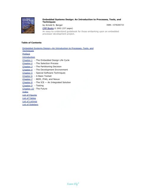
Table of Contents<br />
<strong>Embedded</strong> <strong>Systems</strong> <strong>Design</strong>: <strong>An</strong> <strong>Introduction</strong> <strong>to</strong> Processes, Tools, and<br />
Techniques<br />
by Arnold S. Berger<br />
ISBN: 1578200733<br />
CMP <strong>Book</strong>s © 2002 (237 pages)<br />
<strong>An</strong> easy-<strong>to</strong>-understand guidebook for those embarking upon an embedded<br />
processor development project.<br />
<strong>Embedded</strong> <strong>Systems</strong> <strong>Design</strong>—<strong>An</strong> <strong>Introduction</strong> <strong>to</strong> Processes, Tools, and<br />
Techniques<br />
Preface<br />
<strong>Introduction</strong><br />
Chapter 1 - The <strong>Embedded</strong> <strong>Design</strong> Life Cycle<br />
Chapter 2 - The Selection Process<br />
Chapter 3 - The Partitioning Decision<br />
Chapter 4 - The Development Environment<br />
Chapter 5 - Special Software Techniques<br />
Chapter 6 - A Basic Toolset<br />
Chapter 7 - BDM, JTAG, and Nexus<br />
Chapter 8 - The ICE — <strong>An</strong> Integrated Solution<br />
Chapter 9 - Testing<br />
Chapter 10 - The Future<br />
Index<br />
List of Figures<br />
List of Tables<br />
List of Listings<br />
List of Sidebars<br />
TEAMFLY<br />
Team-Fly ®
<strong>Embedded</strong> <strong>Systems</strong> <strong>Design</strong>—<strong>An</strong><br />
<strong>Introduction</strong> <strong>to</strong> Processes, Tools, and<br />
Techniques<br />
Arnold Berger<br />
CMP <strong>Book</strong>s<br />
CMP Media LLC<br />
1601 West 23rd Street, Suite 200<br />
Lawrence, Kansas 66046<br />
USA<br />
www.cmpbooks.com<br />
<strong>Design</strong>ations used by companies <strong>to</strong> distinguish their products are often claimed as<br />
trademarks. In all instances where CMP <strong>Book</strong>s is aware of a trademark claim, the<br />
product name appears in initial capital letters, in all capital letters, or in<br />
accordance with the vendor’s capitalization preference. Readers should contact the<br />
appropriate companies for more complete information on trademarks and<br />
trademark registrations. All trademarks and registered trademarks in this book are<br />
the property of their respective holders.<br />
Copyright © 2002 by CMP <strong>Book</strong>s, except where noted otherwise. Published by CMP<br />
<strong>Book</strong>s, CMP Media LLC. All rights reserved. Printed in the United States of America.<br />
No part of this publication may be reproduced or distributed in any form or by any<br />
means, or s<strong>to</strong>red in a database or retrieval system, without the prior written<br />
permission of the publisher; with the exception that the program listings may be<br />
entered, s<strong>to</strong>red, and executed in a computer system, but they may not be<br />
reproduced for publication.<br />
The programs in this book are presented for instructional value. The programs<br />
have been carefully tested, but are not guaranteed for any particular purpose. The<br />
publisher does not offer any warranties and does not guarantee the accuracy,<br />
adequacy, or completeness of any information herein and is not responsible for<br />
any errors or omissions. The publisher assumes no liability for damages resulting<br />
from the use of the information in this book or for any infringement of the<br />
intellectual property rights of third parties that would result from the use of this<br />
information.<br />
Developmental<br />
Edi<strong>to</strong>r:<br />
Robert Ward<br />
Edi<strong>to</strong>rs: Matt McDonald, Julie McNamee, Rita Sooby, and<br />
Catherine Janzen<br />
Layout<br />
Production:<br />
Managing Edi<strong>to</strong>r: Michelle O’Neal<br />
Cover Art <strong>Design</strong>: Robert Ward<br />
Distributed in the U.S. and Canada by:<br />
Publishers Group West<br />
1700 Fourth Street<br />
Berkeley, CA 94710<br />
Justin Fulmer, Rita Sooby, and Michelle O’Neal
1-800-788-3123<br />
www.pgw.com<br />
ISBN: 1-57820-073-3<br />
This book is dedicated <strong>to</strong><br />
Shirley Berger.
Preface<br />
Why write a book about designing embedded systems? Because my experiences<br />
working in the industry and, more recently, working with students have convinced<br />
me that there is a need for such a book.<br />
For example, a few years ago, I was the Development Tools Marketing Manager for<br />
a semiconduc<strong>to</strong>r manufacturer. I was speaking with the Software Development<br />
Tools Manager at our major account. My job was <strong>to</strong> help convince the cus<strong>to</strong>mer<br />
that they should be using our RISC processor in their laser printers. Since I owned<br />
the <strong>to</strong>ol chain issues, I had <strong>to</strong> address his specific issues before we could convince<br />
him that we had the appropriate support for his design team.<br />
Since we didn’t have an In-Circuit Emula<strong>to</strong>r for this processor, we found it<br />
necessary <strong>to</strong> create an extended support matrix, built around a ROM emula<strong>to</strong>r,<br />
JTAG port, and a logic analyzer. After explaining all this <strong>to</strong> him, he just shook his<br />
head. I knew I was in trouble. He <strong>to</strong>ld me that, of course, he needed all this stuff.<br />
However, what he really needed was training. The R&D Group had no trouble<br />
hiring all the freshly minted software engineers they needed right out of college.<br />
Finding a new engineer who knew anything about software development outside of<br />
Wintel or UNIX was quite another matter. Thus was born the idea that perhaps<br />
there is some need for a different slant on embedded system design.<br />
Recently I’ve been teaching an introduc<strong>to</strong>ry course at the University of<br />
Washing<strong>to</strong>n-Bothell (UWB). For now, I’m teaching an introduction <strong>to</strong> embedded<br />
systems. Later, there’ll be a lab course. Eventually this course will grow in<strong>to</strong> a full<br />
track, allowing students <strong>to</strong> earn a specialty in embedded systems. Much of this<br />
book’s content is an outgrowth of my work at UWB. Feedback from my students<br />
about the course and its content has influenced the slant of the book. My<br />
interactions with these students and with other faculty have only reinforced my<br />
belief that we need such a book.<br />
What is this book about?<br />
This book is not intended <strong>to</strong> be a text in software design, or even embedded<br />
software design (although it will, of necessity, discuss some code and coding<br />
issues). Most of my students are much better at writing code in C++ and Java<br />
than am I. Thus, my first admission is that I’m not going <strong>to</strong> attempt <strong>to</strong> teach<br />
software methodologies. What I will teach is the how of software development in<br />
an embedded environment. I wrote this book <strong>to</strong> help an embedded software<br />
developer understand the issues that make embedded software development<br />
different from host-based software design. In other words, what do you do when<br />
there is no printf() or malloc()?<br />
Because this is a book about designing embedded systems, I will discuss design<br />
issues — but I’ll focus on those that aren’t encountered in application design. One<br />
of the most significant of these issues is processor selection. One of my<br />
responsibilities as the <strong>Embedded</strong> Tools Marketing Manager was <strong>to</strong> help convince<br />
engineers and their managers <strong>to</strong> use our processors. What are the issues that<br />
surround the choice of the right processor for any given application? Since most<br />
new engineers usually only have architectural knowledge of the Pentium-class, or<br />
SPARC processors, it would be helpful for them <strong>to</strong> broaden their processor horizon.<br />
The correct processor choice can be a “bet the company” decision. I was there in a<br />
few cases where it was such a decision, and the company lost the bet.
Why should you buy this book?<br />
If you are one of my students.<br />
If you’re in my class at UWB, then you’ll probably buy the book because it is on<br />
your required reading list. Besides, an au<strong>to</strong>graphed copy of the book might be<br />
valuable a few years from now (said with a smile). However, the real reason is that<br />
it will simplify note-taking. The content is reasonably faithful <strong>to</strong> the 400 or so<br />
lectures slides that you’ll have <strong>to</strong> sit through in class. Seriously, though, reading<br />
this book will help you <strong>to</strong> get a grasp of the issues that embedded system<br />
designers must deal with on a daily basis. Knowing something about embedded<br />
systems will be a big help when you become a member of the next group and start<br />
looking for a job!<br />
If you are a student elsewhere or a recent graduate.<br />
Even if you aren’t studying embedded systems at UWB, reading this book can be<br />
important <strong>to</strong> your future career. <strong>Embedded</strong> systems is one of the largest and<br />
fastest growing specialties in the industry, but the number of recent graduates<br />
who have embedded experience is woefully small. <strong>An</strong>y prior knowledge of the field<br />
will make you stand out from other job applicants.<br />
As a hiring manager, when interviewing job applicants I would often “tune out” the<br />
candidates who gave the standard, “I’m flexible, I’ll do anything” answer. However,<br />
once in while someone would say, “I used your stuff in school, and boy, was it ever<br />
a kludge. Why did you set up the trace spec menu that way?” That was the<br />
candidate I wanted <strong>to</strong> hire. If your only benefit from reading this book is that you<br />
learn some jargon that helps you make a better impression at your next job<br />
interview, then reading it was probably worth your the time invested.<br />
If you are a working engineer or developer.<br />
If you are an experienced software developer this book will help you <strong>to</strong> see the big<br />
picture. If it’s not in your nature <strong>to</strong> care about the big picture, you may be asking:<br />
“why do I need <strong>to</strong> see the big picture? I’m a software designer. I’m only concerned<br />
with technical issues. Let the marketing-types and managers worry about ‘the big<br />
picture.’ I’ll take a good Quick Sort algorithm anytime.” Well, the reality is that, as<br />
a developer, you are at the bot<strong>to</strong>m of the food chain when it comes <strong>to</strong> making<br />
certain critical decisions, but you are at the <strong>to</strong>p of the blame list when the project<br />
is late. I know from experience. I spent many long hours in the lab trying <strong>to</strong><br />
compensate for a bad decision made by someone else earlier in the project’s<br />
lifecycle. I remember many times when I wasn’t at my daughter’s recitals because<br />
I was fixing code. Don’t let someone else stick you with the dog! This book will<br />
help you recognize and explain the critical importance of certain early decisions. It<br />
will equip you <strong>to</strong> influence the decisions that directly impact your success. You owe<br />
it <strong>to</strong> yourself.<br />
If you are a manager.<br />
Having just maligned managers and marketers, I’m now going <strong>to</strong> take that all back<br />
and say that this book is also for them. If you are a manager and want your<br />
project <strong>to</strong> go smoothly and your product <strong>to</strong> get <strong>to</strong> market on time, then this book<br />
can warn you about land mines and roadblocks. Will it guarantee success? No, but<br />
like chicken soup, it can’t hurt.
I’ll also try <strong>to</strong> share ideas that have worked for me as a manager. For example,<br />
when I was an R&D Project Manager I used a simple “trick” <strong>to</strong> help <strong>to</strong> form my<br />
project team and focus our efforts. Before we even started the product definition<br />
phase I would get some foam-core poster board and build a box with it. The box<br />
had the approximate shape of the product. Then I drew a generic front panel and<br />
pasted it on the front of the box. The front panel had the project’s code name, like<br />
Gerbil, or some other mildly humorous name, prominently displayed. Suddenly, we<br />
had a tangible pro<strong>to</strong>type “image” of the product. We could see it. It got us focused.<br />
Next, I held a pot-luck dinner at my house for the project team and their<br />
significant others. [2] These simple devices helped me <strong>to</strong> bring the team’s focus <strong>to</strong><br />
the project that lay ahead. It also helped <strong>to</strong> form the “extended support team” so<br />
that when the need arose <strong>to</strong> call for a 60 or 80 hours workweek, the home front<br />
support was there.<br />
(While that extended support is important, managers should not abuse it. As an<br />
R&D Manager I realized that I had a large influence over the engineer’s personal<br />
lives. I could impact their salaries with large raises and I could seriously strain a<br />
marriage by firing them. Therefore, I <strong>to</strong>ok my responsibility for delivering the right<br />
product, on time, very seriously. You should <strong>to</strong>o.)<br />
<strong>Embedded</strong> designers and managers shouldn’t have <strong>to</strong> make the same mistakes<br />
over and over. I hope that this book will expose you <strong>to</strong> some of the best practices<br />
that I’ve learned over the years. Since embedded system design seems <strong>to</strong> lie in<br />
the netherworld between Electrical Engineering and Computer Science, some of<br />
the methods and <strong>to</strong>ols that I’ve learned and developed don’t seem <strong>to</strong> rise <strong>to</strong> the<br />
surface in books with a homogeneous focus.<br />
[2] I can't take credit for this idea. I learned if from Controlling Software Projects, by<br />
Tom DeMarco (Yourdon Press, 1982), and from a videotape series of his lectures.<br />
How is the book structured?<br />
For the most part, the text will follow the classic embedded processor lifecycle<br />
model. This model has served the needs of marketing engineers and field sales<br />
engineers for many years. The good news is that this model is a fairly accurate<br />
representation of how embedded systems are developed. While no simple model<br />
truly captures all of the subtleties of the embedded development process,<br />
representing it as a parallel development of hardware and software, followed by an<br />
integration step, seems <strong>to</strong> capture the essence of the process.<br />
What do I expect you <strong>to</strong> know?<br />
Primarily, I assume you are familiar with the vocabulary of application<br />
development. While some familiarity with C, assembly, and basic digital circuits is<br />
helpful, it’s not necessary. The few sections that describe specific C coding<br />
techniques aren’t essential <strong>to</strong> the rest of the book and should be accessible <strong>to</strong><br />
almost any programmer. Similarly, you won’t need <strong>to</strong> be an expert assembly<br />
language programmer <strong>to</strong> understand the point of the examples that are presented<br />
in Mo<strong>to</strong>rola 68000 assembly language. If you have enough logic background <strong>to</strong><br />
understand ANDs and ORs, you are prepared for the circuit content. In short,<br />
anyone who’s had a few college-level programming courses, or equivalent<br />
experience, should be comfortable with the content.
Acknowledgments<br />
I’d like <strong>to</strong> thank some people who helped, directly and indirectly, <strong>to</strong> make this<br />
book a reality. Perry Keller first turned me on <strong>to</strong> the fun and power of the in-circuit<br />
emula<strong>to</strong>r. I’m forever in his debt. Stan Bowlin was the best emula<strong>to</strong>r designer that<br />
I ever had the privilege <strong>to</strong> manage. I learned a lot about how it all works from<br />
Stan. Daniel Mann, an AMD Fellow, helped me <strong>to</strong> understand how all the pieces fit<br />
<strong>to</strong>gether.<br />
The manuscript was edited by Robert Ward, Julie McNamee, Rita Sooby, Michelle<br />
O’Neal, and Catherine Janzen. Justin Fulmer redid many of my graphics. Rita<br />
Sooby and Michelle O’Neal typeset the final result. Finally, Robert Ward and my<br />
friend and colleague, Sid Maxwell, reviewed the manuscript for technical accuracy.<br />
Thank you all.<br />
Arnold Berger<br />
Sammamish, Washing<strong>to</strong>n<br />
September 27, 2001
<strong>Introduction</strong><br />
The arrival of the microprocessor in the 1970s brought about a revolution of<br />
control. For the first time, relatively complex systems could be constructed using a<br />
simple device, the microprocessor, as its primary control and feedback element. If<br />
you were <strong>to</strong> hunt out an old Teletype ASR33 computer terminal in a surplus s<strong>to</strong>re<br />
and compare its innards <strong>to</strong> a modern color inkjet printer, there’s quite a difference.<br />
Au<strong>to</strong>mobile emissions have decreased by 90 percent over the last 20 years,<br />
primarily due <strong>to</strong> the use of microprocessors in the engine-management system.<br />
The open-loop fuel control system, characterized by a carbure<strong>to</strong>r, is now a fuelinjected,<br />
closed-loop system using multiple sensors <strong>to</strong> optimize performance and<br />
minimize emissions over a wide range of operating conditions. This type of<br />
performance improvement would have been impossible without the microprocessor<br />
as a control element.<br />
Microprocessors have now taken over the au<strong>to</strong>mobile. A new luxury- class<br />
au<strong>to</strong>mobile might have more than 70 dedicated microprocessors, controlling tasks<br />
from the engine spark and transmission shift points <strong>to</strong> opening the window slightly<br />
when the door is being closed <strong>to</strong> avoid a pressure burst in the driver’s ear.<br />
The F-16 is an unstable aircraft that cannot be flown without on-board computers<br />
constantly making control surface adjustments <strong>to</strong> keep it in the air. The pilot,<br />
through the traditional controls, sends requests <strong>to</strong> the computer <strong>to</strong> change the<br />
plane’s flight profile. The computer attempts <strong>to</strong> comply with those requests <strong>to</strong> the<br />
extent that it can and still keep the plane in the air.<br />
A modern jetliner can have more than 200 on-board, dedicated microprocessors.<br />
The most exciting driver of microprocessor performance is the games market.<br />
Although it can be argued that the game consoles from Nintendo, Sony, and Sega<br />
are not really embedded systems, the technology boosts that they are driving are<br />
absolutely amazing. Jim Turley[1], at the Microprocessor Forum, described a<br />
200MHz reduced instruction set computer (RISC) processor that was going in<strong>to</strong> a<br />
next-generation game console. This processor could do a four-dimensional matrix<br />
multiplication in one clock cycle at a cost of $25.<br />
Why <strong>Embedded</strong> <strong>Systems</strong> Are Different<br />
Well, all of this is impressive, so let’s delve in<strong>to</strong> what makes embedded systems<br />
design different — at least different enough that someone has <strong>to</strong> write a book<br />
about it. A good place <strong>to</strong> start is <strong>to</strong> try <strong>to</strong> enumerate the differences between your<br />
desk<strong>to</strong>p PC and the typical embedded system.<br />
� <strong>Embedded</strong> systems are dedicated <strong>to</strong> specific tasks, whereas PCs are<br />
generic computing platforms.<br />
� <strong>Embedded</strong> systems are supported by a wide array of processors and<br />
processor architectures.<br />
� <strong>Embedded</strong> systems are usually cost sensitive.<br />
� <strong>Embedded</strong> systems have real-time constraints.
Note You’ll have ample opportunity <strong>to</strong> learn about real time. For now,<br />
real- time events are external (<strong>to</strong> the embedded system) events that<br />
must be dealt with when they occur (in real time).<br />
� If an embedded system is using an operating system at all, it is most<br />
likely using a real-time operating system (RTOS), rather than Windows<br />
9X, Windows NT, Windows 2000, Unix, Solaris, or HP- UX.<br />
� The implications of software failure is much more severe in embedded<br />
systems than in desk<strong>to</strong>p systems.<br />
� <strong>Embedded</strong> systems often have power constraints.<br />
� <strong>Embedded</strong> systems often must operate under extreme environmental<br />
conditions.<br />
� <strong>Embedded</strong> systems have far fewer system resources than desk<strong>to</strong>p<br />
systems.<br />
� <strong>Embedded</strong> systems often s<strong>to</strong>re all their object code in ROM.<br />
� <strong>Embedded</strong> systems require specialized <strong>to</strong>ols and methods <strong>to</strong> be<br />
efficiently designed.<br />
� <strong>Embedded</strong> microprocessors often have dedicated debugging circuitry.<br />
<strong>Embedded</strong> systems are dedicated <strong>to</strong> specific tasks, whereas PCs are<br />
generic computing platforms<br />
<strong>An</strong>other name for an embedded microprocessor is a dedicated microprocessor. It is<br />
programmed <strong>to</strong> perform only one, or perhaps, a few, specific tasks. Changing the<br />
task is usually associated with obsolescing the entire system and redesigning it.<br />
The processor that runs a mobile heart moni<strong>to</strong>r/defibrilla<strong>to</strong>r is not expected <strong>to</strong> run<br />
a spreadsheet or word processor.<br />
Conversely, a general-purpose processor, such as the Pentium on which I’m<br />
working at this moment, must be able <strong>to</strong> support a wide array of applications with<br />
widely varying processing requirements. Because your PC must be able <strong>to</strong> service<br />
the most complex applications with the same performance as the lightest<br />
application, the processing power on your desk<strong>to</strong>p is truly awesome.<br />
Thus, it wouldn’t make much sense, either economically or from an engineering<br />
standpoint, <strong>to</strong> put an AMD-K6, or similar processor, inside the coffeemaker on your<br />
kitchen counter.<br />
Note That’s not <strong>to</strong> say that someone won’t do something similar. For<br />
example, a French company designed a vacuum cleaner with an<br />
AMD 29000 processor. The 29000 is a 32-bit RISC CPU that is far<br />
more suited for driving laser-printer engines.<br />
<strong>Embedded</strong> systems are supported by a wide array of processors and<br />
processor architectures<br />
Most students who take my Computer Architecture or <strong>Embedded</strong> <strong>Systems</strong> class<br />
have never programmed on any platform except the X86 (Intel) or the Sun SPARC<br />
family. The students who take the <strong>Embedded</strong> <strong>Systems</strong> class are rudely awakened<br />
by their first homework assignment, which has them researching the available<br />
trade literature and proposing the optimal processor for an assigned application.
These students are learning that <strong>to</strong>day more than 140 different microprocessors<br />
are available from more than 40 semiconduc<strong>to</strong>r vendors[2]. These vendors are in a<br />
daily battle with each other <strong>to</strong> get the design-win (be the processor of choice) for<br />
the next wide-body jet or the next Internet- based soda machine.<br />
In Chapter 2, you’ll learn more about the processor-selection process. For now,<br />
just appreciate the range of available choices.<br />
<strong>Embedded</strong> systems are usually cost sensitive<br />
I say “usually” because the cost of the embedded processor in the Mars Rover was<br />
probably not on the design team’s <strong>to</strong>p 10 list of constraints. However, if you save<br />
10 cents on the cost of the Engine Management Computer System, you’ll be a hero<br />
at most au<strong>to</strong>mobile companies. Cost does matter in most embedded applications.<br />
The cost that you must consider most of the time is system cost. The cost of the<br />
processor is a fac<strong>to</strong>r, but, if you can eliminate a printed circuit board and<br />
connec<strong>to</strong>rs and get by with a smaller power supply by using a highly integrated<br />
microcontroller instead of a microprocessor and separate peripheral devices, you<br />
have potentially a greater reduction in system costs, even if the integrated device<br />
is significantly more costly than the discrete device. This issue is covered in more<br />
detail in Chapter 3.<br />
<strong>Embedded</strong> systems have real-time constraints<br />
I was thinking about how <strong>to</strong> introduce this section when my lap<strong>to</strong>p decided <strong>to</strong> back<br />
up my work. I started <strong>to</strong> type but was faced with the hourglass symbol because<br />
the computer was busy doing other things. Suppose my computer wasn’t sitting on<br />
my desk but was connected <strong>to</strong> a radar antenna in the nose of a commercial jetliner.<br />
If the computer’s main function in life is <strong>to</strong> provide a collision alert warning, then<br />
suspending that task could be disastrous.<br />
Real-time constraints generally are grouped in<strong>to</strong> two categories: time- sensitive<br />
constraints and time-critical constraints. If a task is time critical, it must take place<br />
within a set window of time, or the function controlled by that task fails.<br />
Controlling the flight-worthiness of an aircraft is a good example of this. If the<br />
feedback loop isn’t fast enough, the control algorithm becomes unstable, and the<br />
aircraft won’t stay in the air.<br />
A time-sensitive task can die gracefully. If the task should take, for example,<br />
4.5ms but takes, on average, 6.3ms, then perhaps the inkjet printer will print two<br />
pages per minute instead of the design goal of three pages per minute.<br />
If an embedded system is using an operating system at all, it is most<br />
likely using an RTOS<br />
Like embedded processors, embedded operating systems also come in a wide<br />
variety of flavors and colors. My students must also pick an embedded operating<br />
system as part of their homework project. RTOSs are not democratic. They need<br />
not give every task that is ready <strong>to</strong> execute the time it needs. RTOSs give the<br />
highest priority task that needs <strong>to</strong> run all the time it needs. If other tasks fail <strong>to</strong><br />
get sufficient CPU time, it’s the programmer’s problem.
<strong>An</strong>other difference between most commercially available operating systems and<br />
your desk<strong>to</strong>p operating system is something you won’t get with an RTOS. You<br />
won’t get the dreaded Blue Screen of Death that many Windows 9X users see on a<br />
regular basis.<br />
The implications of software failure are much more severe in embedded<br />
systems than in desk<strong>to</strong>p systems<br />
Remember the Y2K hysteria? The people who were really under the gun were the<br />
people responsible for the continued good health of our computer- based<br />
infrastructure. A lot of money was spent searching out and replacing devices with<br />
embedded processors because the #$%%$ thing got the dates all wrong.<br />
We all know of the tragic consequences of a medical radiation machine that<br />
miscalculates a dosage. How do we know when our code is bug free? How do you<br />
completely test complex software that must function properly under all conditions?<br />
However, the most important point <strong>to</strong> take away from this discussion is that<br />
software failure is far less <strong>to</strong>lerable in an embedded system than in your average<br />
desk<strong>to</strong>p PC. That is not <strong>to</strong> imply that software never fails in an embedded system,<br />
just that most embedded systems typically contain some mechanism, such as a<br />
watchdog timer, <strong>to</strong> bring it back <strong>to</strong> life if the software loses control. You’ll find out<br />
more about software testing in Chapter 9.<br />
<strong>Embedded</strong> systems have power constraints<br />
For many readers, the only CPU they have ever seen is the Pentium or AMD K6<br />
inside their desk<strong>to</strong>p PC. The CPU needs a massive heat sink and fan assembly <strong>to</strong><br />
keep the processor from baking itself <strong>to</strong> death. This is not a particularly serious<br />
constraint for a desk<strong>to</strong>p system. Most desk<strong>to</strong>p PC’s have plenty of spare space<br />
inside <strong>to</strong> allow for good airflow. However, consider an embedded system attached<br />
<strong>to</strong> the collar of a wolf roaming around Wyoming or Montana. These systems must<br />
work reliably and for a long time on a set of small batteries.<br />
TEAMFLY<br />
How do you keep your embedded system running on minute amounts of power?<br />
Usually that task is left up <strong>to</strong> the hardware engineer. However, the division of<br />
responsibility isn’t clearly delineated. The hardware designer might or might not<br />
have some idea of the software architectural constraints. In general, the processor<br />
choice is determined outside the range of hearing of the software designers. If the<br />
overall system design is on a tight power budget, it is likely that the software<br />
design must be built around a system in which the processor is in “sleep mode”<br />
most of the time and only wakes up when a timer tick occurs. In other words, the<br />
system is completely interrupt driven.<br />
Power constraints impact every aspect of the system design decisions. Power<br />
constraints affect the processor choice, its speed, and its memory architecture.<br />
The constraints imposed by the system requirements will likely determine whether<br />
the software must be written in assembly language, rather than C or C++,<br />
because the absolute maximum performance must be achieved within the power<br />
budget. Power requirements are dictated by the CPU clock speed and the number<br />
of active electronic components (CPU, RAM, ROM, I/O devices, and so on).<br />
Thus, from the perspective of the software designer, the power constraints could<br />
become the dominant system constraint, dictating the choice of software <strong>to</strong>ols,<br />
memory size, and performance headroom.<br />
Team-Fly ®
Speed vs. Power<br />
Almost all modern CPUs are fabricated using the Complementary Metal Oxide<br />
Silicon (CMOS) process. The simple gate structure of CMOS devices consists of two<br />
MOS transis<strong>to</strong>rs, one N-type and one P-type (hence, the term complementary),<br />
stacked like a <strong>to</strong>tem pole with the N-type on <strong>to</strong>p and the P-type on the bot<strong>to</strong>m.<br />
Both transis<strong>to</strong>rs behave like perfect switches. When the output is high, or logic<br />
level 1, the P-type transis<strong>to</strong>r is turned off, and the N-type transis<strong>to</strong>r connects the<br />
output <strong>to</strong> the supply voltage (5V, 3.3V, and so on), which the gate outputs <strong>to</strong> the<br />
rest of the circuit.<br />
When the logic level is 0, the situation is reversed, and the P-type transis<strong>to</strong>r<br />
connects the next stage <strong>to</strong> ground while the N-type transis<strong>to</strong>r is turned off. This<br />
circuit <strong>to</strong>pology has an interesting property that makes it attractive from a power-<br />
use viewpoint. If the circuit is static (not changing state), the power loss is<br />
extremely small. In fact, it would be zero if not for a small amount of leakage<br />
current inherent in these devices at normal room temperature and above.<br />
When the circuit is switching, as in a CPU, things are different. While a gate<br />
switches logic levels, there is a period of time when the N-type and P-type<br />
transis<strong>to</strong>rs are simultaneously on. During this brief window, current can flow from<br />
the supply voltage line <strong>to</strong> ground through both devices. Current flow means power<br />
dissipation and that means heat. The greater the clock speed, the greater the<br />
number of switching cycles taking place per second, and this means more power<br />
loss. Now, consider your 500MHz Pentium or Athlon processor with 10 million or so<br />
transis<strong>to</strong>rs, and you can see why these desk<strong>to</strong>p machines are so power hungry. In<br />
fact, it is almost a perfect linear relationship between CPU speed and power<br />
dissipation in modern processors. Those of you who overclock your CPUs <strong>to</strong> wring<br />
every last ounce of performance out of it know how important a good heat sink<br />
and fan combination are.<br />
<strong>Embedded</strong> systems must operate under extreme environmental conditions<br />
<strong>Embedded</strong> systems are everywhere. Everywhere means everywhere. <strong>Embedded</strong><br />
systems must run in aircraft, in the polar ice, in outer space, in the trunk of a<br />
black Camaro in Phoenix, Arizona, in August. Although making sure that the<br />
system runs under these conditions is usually the domain of the hardware designer,<br />
there are implications for both the hardware and software. Harsh environments<br />
usually mean more than temperature and humidity. Devices that are qualified for<br />
military use must meet a long list of environmental requirements and have the<br />
documentation <strong>to</strong> prove it. If you’ve wondered why a simple processor, such as the<br />
8086 from Intel, should cost several thousands of dollars in a missile, think<br />
paperwork and environment. The fact that a device must be qualified for the<br />
environment in which it will be operating, such as deep space, often dictates the<br />
selection of devices that are available.<br />
The environmental concerns often overlap other concerns, such as power<br />
requirements. Sealing a processor under a silicone rubber conformal coating<br />
because it must be environmentally sealed also means that the capability <strong>to</strong><br />
dissipate heat is severely reduced, so processor type and speed is also a fac<strong>to</strong>r.<br />
Unfortunately, the environmental constraints are often left <strong>to</strong> the very end of the<br />
project, when the product is in testing and the hardware designer discovers that<br />
the product is exceeding its thermal budget. This often means slowing the clock,<br />
which leads <strong>to</strong> less time for the software <strong>to</strong> do its job, which translates <strong>to</strong> further
efining the software <strong>to</strong> improve the efficiency of the code. All the while, the<br />
product is still not released.<br />
<strong>Embedded</strong> systems have far fewer system resources than desk<strong>to</strong>p<br />
systems<br />
Right now, I’m typing this manuscript on my desk<strong>to</strong>p PC. <strong>An</strong> oldies CD is playing<br />
through the speakers. I’ve got 256MB of RAM, 26GB of disk space, and assorted<br />
ZIP, JAZZ, floppy, and CD-RW devices on a SCSI card. I’m looking at a beautiful<br />
19-inch CRT moni<strong>to</strong>r. I can enter data through a keyboard and a mouse. Just<br />
considering the bus signals in the system, I have the following:<br />
� Processor bus<br />
� AGP bus<br />
� PCI bus<br />
� ISA bus<br />
� SCSI bus<br />
� USB bus<br />
� Parallel bus<br />
� RS-232C bus<br />
<strong>An</strong> awful lot of system resources are at my disposal <strong>to</strong> make my computing chores<br />
as painless as possible. It is a tribute <strong>to</strong> the technological and economic driving<br />
forces of the PC industry that so much computing power is at my fingertips.<br />
Now consider the embedded system controlling your VCR. Obviously, it has far<br />
fewer resources that it must manage than the desk<strong>to</strong>p example. Of course, this is<br />
because it is dedicated <strong>to</strong> a few well-defined tasks and nothing else. Being<br />
engineered for cost effectiveness (the whole VCR only cost $80 retail), you can’t<br />
expect the CPU <strong>to</strong> be particularly general purpose. This translates <strong>to</strong> fewer<br />
resources <strong>to</strong> manage and hence, lower cost and simplicity. However, it also means<br />
that the software designer is often required <strong>to</strong> design standard input and output<br />
(I/O) routines repeatedly. The number of inputs and outputs are usually so limited,<br />
the designers are forced <strong>to</strong> overload and serialize the functions of one or two input<br />
devices. Ever try <strong>to</strong> set the time in your super exercise workout wristwatch after<br />
you’ve misplaced the instruction sheet?<br />
<strong>Embedded</strong> systems s<strong>to</strong>re all their object code in ROM<br />
Even your PC has <strong>to</strong> s<strong>to</strong>re some of its code in ROM. ROM is needed in almost all<br />
systems <strong>to</strong> provide enough code for the system <strong>to</strong> initialize itself (boot-up code).<br />
However, most embedded systems must have all their code in ROM. This means<br />
severe limitations might be imposed on the size of the code image that will fit in<br />
the ROM space. However, it’s more likely that the methods used <strong>to</strong> design the<br />
system will need <strong>to</strong> be changed because the code is in ROM.<br />
As an example, when the embedded system is powered up, there must be code<br />
that initializes the system so that the rest of the code can run. This means<br />
establishing the run-time environment, such as initializing and placing variables in<br />
RAM, testing memory integrity, testing the ROM integrity with a checksum test,<br />
and other initialization tasks.
From the point of view of debugging the system, ROM code has certain<br />
implications. First, your handy debugger is not able <strong>to</strong> set a breakpoint in ROM. To<br />
set a breakpoint, the debugger must be able <strong>to</strong> remove the user’s instruction and<br />
replace it with a special instruction, such as a TRAP instruction or software<br />
interrupt instruction. The TRAP forces a transfer <strong>to</strong> a convenient entry point in the<br />
debugger. In some systems, you can get around this problem by loading the<br />
application software in<strong>to</strong> RAM. Of course, this assumes sufficient RAM is available<br />
<strong>to</strong> hold of all the applications, <strong>to</strong> s<strong>to</strong>re variables, and <strong>to</strong> provide for dynamic<br />
memory allocation.<br />
Of course, being a capitalistic society, wherever there is a need, someone will<br />
provide a solution. In this case, the specialized suite of <strong>to</strong>ols that have evolved <strong>to</strong><br />
support the embedded system development process gives you a way around this<br />
dilemma, which is discussed in the next section.<br />
<strong>Embedded</strong> systems require specialized <strong>to</strong>ols and methods <strong>to</strong> be efficiently<br />
designed<br />
Chapters 4 through 8 discuss the types of <strong>to</strong>ols in much greater detail. The<br />
embedded system is so different in so many ways, it’s not surprising that<br />
specialized <strong>to</strong>ols and methods must be used <strong>to</strong> create and test embedded software.<br />
Take the case of the previous example—the need <strong>to</strong> set a break-point at an<br />
instruction boundary located in ROM.<br />
A ROM Emula<strong>to</strong>r<br />
Several companies manufacture hardware-assist products, such as ROM emula<strong>to</strong>rs.<br />
Figure 1 shows a product called NetROM, from Applied Microsystems Corporation.<br />
NetROM is an example of a general class of <strong>to</strong>ols called emula<strong>to</strong>rs. From the point<br />
of view of the target system, the ROM emula<strong>to</strong>r is designed <strong>to</strong> look like a standard<br />
ROM device. It has a connec<strong>to</strong>r that has the exact mechanical dimensions and<br />
electrical characteristics of the ROM it is emulating. However, the connec<strong>to</strong>r’s job<br />
is <strong>to</strong> bring the signals from the ROM socket on the target system <strong>to</strong> the main<br />
circuitry, located at the other end of the cable. This circuitry provides high-speed<br />
RAM that can be written <strong>to</strong> quickly via a separate channel from a host computer.<br />
Thus, the target system sees a ROM device, but the software developer sees a<br />
RAM device that can have its code easily modified and allows debugger<br />
breakpoints <strong>to</strong> be set.<br />
Figure 1: NetROM.
Note In the context of this book, the term hardware-assist refers <strong>to</strong><br />
additional specialized devices that supplement a software-only<br />
debugging solution. A ROM emula<strong>to</strong>r, manufactured by companies<br />
such as Applied Microsystems and Grammar Engine, is an example<br />
of a hardware-assist device.<br />
<strong>Embedded</strong> microprocessors often have dedicated debugging circuitry<br />
Perhaps one of the most dramatic differences between <strong>to</strong>day’s embedded<br />
microprocessors and those of a few years ago is the almost manda<strong>to</strong>ry inclusion of<br />
dedicated debugging circuitry in silicon on the chip. This is almost counter-intuitive<br />
<strong>to</strong> all of the previous discussion. After droning on about the cost sensitivity of<br />
embedded systems, it seems almost foolish <strong>to</strong> think that every microprocessor in<br />
production contains circuitry that is only necessary for debugging a product under<br />
development. In fact, this was the prevailing sentiment for a while. <strong>Embedded</strong>-chip<br />
manufacturers actually built special versions of their embedded devices that<br />
contained the debug circuitry and made them available (or not available) <strong>to</strong> their<br />
<strong>to</strong>ol suppliers. In the end, most manufacturers found it more cost-effective <strong>to</strong><br />
produce one version of the chip for all purposes. This didn’t s<strong>to</strong>p them from<br />
restricting the information about how the debug circuitry worked, but every device<br />
produced did contain the debug “hooks” for the hardware-assist <strong>to</strong>ols.<br />
What is noteworthy is that the manufacturers all realized that the inclusion of onchip<br />
debug circuitry was a requirement for acceptance of their devices in an<br />
embedded application. That is, unless their chip had a good solution for embedded<br />
system design and debug, it was not going <strong>to</strong> be a serious contender for an<br />
embedded application by a product-development team facing time-<strong>to</strong>-market<br />
pressures.<br />
Summary<br />
Now that you know what is different about embedded systems, it’s time <strong>to</strong> see<br />
how you actually tame the beast. In the chapters that follow, you’ll examine the<br />
embedded system design process step by step, as it is practiced.<br />
The first few chapters focus on the process itself. I’ll describe the design life cycle<br />
and examine the issues affecting processor selection. The later chapters focus on<br />
techniques and <strong>to</strong>ols used <strong>to</strong> build, test, and debug a complete system.<br />
I’ll close with some comments on the business of embedded systems and on an<br />
emerging technology that might change everything.<br />
Although engineers like <strong>to</strong> think design is a rational, requirements-driven process,<br />
in the real world, many decisions that have an enormous impact on the design<br />
process are made by non-engineers based on criteria that might have little <strong>to</strong> do<br />
with the project requirements. For example, in many projects, the decision <strong>to</strong> use<br />
a particular processor has nothing <strong>to</strong> do with the engineering parameters of the<br />
problem. Too often, it becomes the task of the design team <strong>to</strong> pick up the pieces<br />
and make these decisions work. Hopefully, this book provides some ammunition <strong>to</strong><br />
those frazzled engineers who often have <strong>to</strong> make do with less than optimal<br />
conditions.
Works Cited<br />
1. Turley, Jim. “High Integration is Key for Major <strong>Design</strong> Wins.” A paper<br />
presented at the <strong>Embedded</strong> Processor Forum, San Jose, 15 Oc<strong>to</strong>ber<br />
1998.<br />
2. Levy, Marcus. “EDN Microprocessor/Microcontroller Direc<strong>to</strong>ry.” EDN, 14<br />
September 2000.
Chapter 1: The <strong>Embedded</strong> <strong>Design</strong> Life<br />
Cycle<br />
Unlike the design of a software application on a standard platform, the design of<br />
an embedded system implies that both software and hardware are being designed<br />
in parallel. Although this isn’t always the case, it is a reality for many designs<br />
<strong>to</strong>day. The profound implications of this simultaneous design process heavily<br />
influence how systems are designed.<br />
<strong>Introduction</strong><br />
Figure 1.1 provides a schematic representation of the embedded design life cycle<br />
(which has been shown ad nauseam in marketing presentations).<br />
Figure 1.1: <strong>Embedded</strong> design life cycle diagram.<br />
A phase representation of the embedded design life cycle.<br />
Time flows from the left and proceeds through seven phases:<br />
� Product specification<br />
� Partitioning of the design in<strong>to</strong> its software and hardware components<br />
� Iteration and refinement of the partitioning<br />
� Independent hardware and software design tasks<br />
� Integration of the hardware and software components<br />
� Product testing and release<br />
� On-going maintenance and upgrading
The embedded design process is not as simple as Figure 1.1 depicts. A<br />
considerable amount of iteration and optimization occurs within phases and<br />
between phases. Defects found in later stages often cause you <strong>to</strong> “go back <strong>to</strong><br />
square 1.” For example, when product testing reveals performance deficiencies<br />
that render the design non-competitive, you might have <strong>to</strong> rewrite algorithms,<br />
redesign cus<strong>to</strong>m hardware — such as Application-Specific Integrated Circuits<br />
(ASICs) for better performance — speed up the processor, choose a new processor,<br />
and so on.<br />
Although this book is generally organized according <strong>to</strong> the life-cycle view in Figure<br />
1.1, it can be helpful <strong>to</strong> look at the process from other perspectives. Dr. Daniel<br />
Mann, Advanced Micro Devices (AMD), Inc., has developed a <strong>to</strong>ol-based view of<br />
the development cycle. In Mann’s model, processor selection is one of the first<br />
tasks (see Figure 1.2). This is understandable, considering the selection of the<br />
right processor is of prime importance <strong>to</strong> AMD, a manufacturer of embedded<br />
microprocessors. However, it can be argued that including the choice of the<br />
microprocessor and some of the other key elements of a design in the specification<br />
phase is the correct approach. For example, if your existing code base is written<br />
for the 80X86 processor family, it’s entirely legitimate <strong>to</strong> require that the next<br />
design also be able <strong>to</strong> leverage this code base. Similarly, if your design team is<br />
highly experienced using the Green Hills© compiler, your requirements document<br />
probably would specify that compiler as well.<br />
Figure 1.2: Tools used in the design process.<br />
The embedded design cycle represented in terms of the <strong>to</strong>ols used in the<br />
design process (courtesy of Dr. Daniel Mann, AMD Fellow, Advanced Micro<br />
Devices, Inc., Austin, TX).<br />
The economics and reality of a design requirement often force decisions <strong>to</strong> be<br />
made before designers can consider the best design trade-offs for the next project.<br />
In fact, designers use the term “clean sheet of paper” when referring <strong>to</strong> a design<br />
opportunity in which the requirement constraints are minimal and can be strictly<br />
specified in terms of performance and cost goals.
Figure 1.2 shows the maintenance and upgrade phase. The engineers are<br />
responsible for maintaining and improving existing product designs until the<br />
burden of new features and requirements overwhelms the existing design. Usually,<br />
these engineers were not the same group that designed the original product. It’s a<br />
miracle if the original designers are still around <strong>to</strong> answer questions about the<br />
product. Although more engineers maintain and upgrade projects than create new<br />
designs, few, if any, <strong>to</strong>ols are available <strong>to</strong> help these designers reverse-engineer<br />
the product <strong>to</strong> make improvements and locate bugs. The <strong>to</strong>ols used for<br />
maintenance and upgrading are the same <strong>to</strong>ols designed for engineers creating<br />
new designs.<br />
The remainder of this book is devoted <strong>to</strong> following this life cycle through the stepby-step<br />
development of embedded systems. The following sections give an<br />
overview of the steps in Figure 1.1.<br />
Product Specification<br />
Although this book isn’t intended as a marketing manual, learning how <strong>to</strong> design<br />
an embedded system should include some consideration of designing the right<br />
embedded system. For many R&D engineers, designing the right product means<br />
cramming everything possible in<strong>to</strong> the product <strong>to</strong> make sure they don’t miss<br />
anything. Obviously, this wastes time and resources, which is why marketing and<br />
sales departments lead (or completely execute) the product-specification process<br />
for most companies. The R&D engineers usually aren’t allowed cus<strong>to</strong>mer contact in<br />
this early stage of the design. This shortsighted policy prevents the product design<br />
engineers from acquiring a useful cus<strong>to</strong>mer perspective about their products.<br />
Although some methods of cus<strong>to</strong>mer research, such as questionnaires and focus<br />
groups, clearly belong in the realm of marketing specialists, most projects benefit<br />
from including engineers in some market-research activities, especially the<br />
cus<strong>to</strong>mer visit or cus<strong>to</strong>mer research <strong>to</strong>ur.<br />
The Ideal Cus<strong>to</strong>mer Research Tour<br />
The ideal research team is three or four people, usually a marketing or sales<br />
engineer and two or three R&D types. Each member of the team has a specific role<br />
during the visit. Often, these roles switch among the team members so each has<br />
an opportunity <strong>to</strong> try all the roles. The team prepares for the visit by developing a<br />
questionnaire <strong>to</strong> use <strong>to</strong> keep the interviews flowing smoothly. In general, the<br />
questionnaire consists of a set of open-ended questions that the team members fill<br />
in as they speak with the cus<strong>to</strong>mers. For several cus<strong>to</strong>mer visits, my research<br />
team spent more than two weeks preparing and refining the questionnaire.<br />
(Considering the cost of a cus<strong>to</strong>mer visit <strong>to</strong>ur (about $1,000 per day, per person<br />
for airfare, hotels, meals, and loss of productivity), it’s amazing how often little<br />
effort is put in<strong>to</strong> preparing for the visit. Although it makes sense <strong>to</strong> visit your<br />
cus<strong>to</strong>mers and get inside their heads, it makes more sense <strong>to</strong> prepare properly for<br />
the research <strong>to</strong>ur.)<br />
The lead interviewer is often the marketing person, although it doesn’t have <strong>to</strong> be.<br />
The second team member takes notes and asks follow-up questions or digs down<br />
even deeper. The remaining team members are observers and technical resources.<br />
If the discussion centers on technical issues, the other team members might have<br />
<strong>to</strong> speak up, especially if the discussion concerns their area of expertise. However,<br />
their primary function is <strong>to</strong> take notes, listen carefully, and look around as much as<br />
possible.
After each visit ends, the team meets off-site for a debriefing. The debriefing step<br />
is as important as the visit itself <strong>to</strong> make sure the team members retain the<br />
following:<br />
� What did each member hear?<br />
� What was explicitly stated? What was implicit?<br />
� Did they like what we had or were they being polite?<br />
� Was someone really turned on by it?<br />
� Did we need <strong>to</strong> refine our presentation or the form of the questionnaire?<br />
� Were we talking <strong>to</strong> the right people?<br />
As the debriefing continues, team members take additional notes and jot down<br />
thoughts. At the end of the day, one team member writes a summary of the visit’s<br />
results.<br />
After returning from the <strong>to</strong>ur, the effort focuses on translating what the team<br />
heard from the cus<strong>to</strong>mers in<strong>to</strong> a set of product requirements <strong>to</strong> act on. These<br />
sessions are often the most difficult and the most fun. The team often is<br />
passionate in its arguments for the cus<strong>to</strong>mers and equally passionate that the<br />
cus<strong>to</strong>mers don’t know what they want. At some point in this process, the<br />
information from the visit is distilled down <strong>to</strong> a set of requirements <strong>to</strong> guide the<br />
team through the product development phase.<br />
Often, teams single out one or more cus<strong>to</strong>mers for a second or third visit as the<br />
product development progresses. These visits provide a reality check and some<br />
midcourse corrections while the impact of the changes are minimal.<br />
Participating in the cus<strong>to</strong>mer research <strong>to</strong>ur as an R&D engineer on the project has<br />
a side benefit. Not only do you have a design specification (hopefully) against<br />
which <strong>to</strong> design, you also have a picture in your mind’s eye of your team’s ultimate<br />
objective. A little voice in your ear now biases your endless design decisions<br />
<strong>to</strong>ward the common goals of the design team. This extra insight in<strong>to</strong> the product<br />
specifications can significantly impact the success of the project.<br />
A senior engineering manager studied projects within her company that were<br />
successful not only in the marketplace but also in the execution of the productdevelopment<br />
process. Many of these projects were embedded systems. Also, she<br />
studied projects that had failed in the market or in the development process.<br />
Flight Deck on the Bass Boat?<br />
Having spent the bulk of my career as an R&D engineer and manager, I am<br />
continually fascinated by the process of turning a concept in<strong>to</strong> a product. Knowing<br />
how <strong>to</strong> ask the right questions of a potential cus<strong>to</strong>mer, understanding his needs,<br />
determining the best feature and price point, and handling all the other details of<br />
research are not easy, and certainly not straightforward <strong>to</strong> number-driven<br />
engineers.<br />
One of the most valuable classes I ever attended was conducted by a marketing<br />
professor at Santa Clara University on how <strong>to</strong> conduct cus<strong>to</strong>mer research. I
learned that the cus<strong>to</strong>mer wants everything yesterday and is unwilling <strong>to</strong> pay for<br />
any of it. If you ask a cus<strong>to</strong>mer whether he wants a feature, he’ll say yes every<br />
time. So, how do you avoid building an aircraft carrier when the cus<strong>to</strong>mer really<br />
needs a fishing boat? First of all, don’t ask the cus<strong>to</strong>mer whether the product<br />
should have a flight deck. Focus your efforts on understanding what the cus<strong>to</strong>mer<br />
wants <strong>to</strong> accomplish and then extend his requirements <strong>to</strong> your product. As a result,<br />
the product and features you define are an abstraction and a distillation of the<br />
needs of your cus<strong>to</strong>mer.<br />
A common fac<strong>to</strong>r for the successful products was that the design team shared a<br />
common vision of the product they were designing. When asked about the product,<br />
everyone involved — senior management, marketing, sales, quality assurance, and<br />
engineering — would provide the same general description. In contrast, many<br />
failed products did not produce a consistent articulation of the project goals. One<br />
engineer thought it was supposed <strong>to</strong> be a low-cost product with medium<br />
performance. <strong>An</strong>other thought it was <strong>to</strong> be a high-performance, medium-cost<br />
product, with the objective <strong>to</strong> maximize the performance-<strong>to</strong>-cost ratio. A third felt<br />
the goal was <strong>to</strong> get something <strong>to</strong>gether in a hurry and put it in<strong>to</strong> the market as<br />
soon as possible.<br />
<strong>An</strong>other often-overlooked part of the product-specification phase is the<br />
development <strong>to</strong>ols required <strong>to</strong> design the product. Figure 1.2 shows the embedded<br />
life cycle from a different perspective. This “design <strong>to</strong>ols view” of the development<br />
cycle highlights the variety of <strong>to</strong>ols needed by embedded developers.<br />
When I designed in-circuit emula<strong>to</strong>rs, I saw products that were late <strong>to</strong> market<br />
because the engineers did not have access <strong>to</strong> the best <strong>to</strong>ols for the job. For<br />
example, only a third of the hard-core embedded developers ever used in-circuit<br />
emula<strong>to</strong>rs, even though they were the <strong>to</strong>ols of choice for difficult debugging<br />
problems.<br />
TEAMFLY<br />
The development <strong>to</strong>ols requirements should be part of the product specification <strong>to</strong><br />
ensure that unreal expectations aren’t being set for the product development cycle<br />
and <strong>to</strong> minimize the risk that the design team won’t meet its goals.<br />
Tip One of the smartest project development methods of which I’m<br />
aware is <strong>to</strong> begin each team meeting or project review meeting by<br />
showing a list of the project musts and wants. Every project<br />
stakeholder must agree that the list is still valid. If things have<br />
changed, then the project manager declares the project on hold until<br />
the differences are resolved. In most cases, this means that the<br />
project schedule and deliverables are no longer valid. When this<br />
happens, it’s a big deal—comparable <strong>to</strong> an assembly line worker in<br />
an au<strong>to</strong> plant s<strong>to</strong>pping the line because something is not right with<br />
the manufacturing process of the car.<br />
In most cases, the differences are easily resolved and work continues, but not<br />
always. Sometimes a competi<strong>to</strong>r may force a re-evaluation of the product features.<br />
Sometimes, technologies don’t pan out, and an alternative approach must be<br />
found. Since the alternative approach is generally not as good as the primary<br />
approach, design compromises must be fac<strong>to</strong>red in.<br />
Team-Fly ®
Hardware/Software Partitioning<br />
Since an embedded design will involve both hardware and software components,<br />
someone must decide which portion of the problem will be solved in hardware and<br />
which in software. This choice is called the "partitioning decision."<br />
Application developers, who normally work with pre-defined hardware resources,<br />
may have difficulty adjusting <strong>to</strong> the notion that the hardware can be enhanced <strong>to</strong><br />
address any arbitrary portion of the problem. However, they've probably already<br />
encountered examples of such a hardware/software tradeoff. For example, in the<br />
early days of the PC (i.e., before the introduction of the 80486 processor), the<br />
8086, 80286, and 80386 CPUs didn’t have an on-chip floating-point processing<br />
unit. These processors required companion devices, the 8087, 80287, and 80387<br />
floating-point units (FPUs), <strong>to</strong> directly execute the floating-point instructions in the<br />
application code.<br />
If the PC did not have an FPU, the application code had <strong>to</strong> trap the floating-point<br />
instructions and execute an exception or trap routine <strong>to</strong> emulate the behavior of<br />
the hardware FPU in software. Of course, this was much slower than having the<br />
FPU on your motherboard, but at least the code ran.<br />
As another example of hardware/software partitioning, you can purchase a modem<br />
card for your PC that plugs in<strong>to</strong> an ISA slot and contains the<br />
modulation/demodulation circuitry on the board. For less money, however, you can<br />
purchase a Winmodem that plugs in<strong>to</strong> a PCI slot and uses your PC’s CPU <strong>to</strong> directly<br />
handle the modem functions. Finally, if you are a dedicated PC gamer, you know<br />
how important a high-performance video card is <strong>to</strong> game speed.<br />
If you generalize the concept of the algorithm <strong>to</strong> the steps required <strong>to</strong> implement a<br />
design, you can think of the algorithm as a combination of hardware components<br />
and software components. Each of these hardware/software partitioning examples<br />
implements an algorithm. You can implement that algorithm purely in software<br />
(the CPU without the FPU example), purely in hardware (the dedicated modem<br />
chip example), or in some combination of the two (the video card example).<br />
Laser Printer <strong>Design</strong> Algorithm<br />
Suppose your embedded system design task is <strong>to</strong> develop a laser printer. Figure<br />
1.3 shows the algorithm for this project. With help from laser printer designers,<br />
you can imagine how this task might be accomplished in software. The processor<br />
places the incoming data stream — via the parallel port, RS-232C serial port, USB<br />
port, or Ethernet port — in<strong>to</strong> a memory buffer.
Figure 1.3: The laser printer design.<br />
A laser printer design as an algorithm. Data enters the printer and must<br />
be transformed in<strong>to</strong> a legible ensemble of carbon dots fused <strong>to</strong> a piece of<br />
paper.<br />
Concurrently, the processor services the data port and converts the incoming data<br />
stream in<strong>to</strong> a stream of modulation and control signals <strong>to</strong> a laser tube, rotating<br />
mirror, rotating drum, and assorted paper-management “stuff.” You can see how<br />
this would bog down most modern microprocessors and limit the performance of<br />
the system.<br />
You could try <strong>to</strong> improve performance by adding more processors, thus dividing<br />
the concurrent tasks among them. This would speed things up, but without more<br />
information, it’s hard <strong>to</strong> determine whether that would be an optimal solution for<br />
the algorithm.<br />
When you analyze the algorithm, however, you see that certain tasks critical <strong>to</strong> the<br />
performance of the system are also bounded and well-defined. These tasks can be<br />
easily represented by design methods that can be translated <strong>to</strong> a hardware-based<br />
solution. For this laser printer design, you could dedicate a hardware block <strong>to</strong> the<br />
process of writing the laser dots on<strong>to</strong> the pho<strong>to</strong>sensitive surface of the printer<br />
drum. This frees the processor <strong>to</strong> do other tasks and only requires it <strong>to</strong> initialize<br />
and service the hardware if an error is detected.<br />
This seems like a fruitful approach until you dig a bit deeper. The requirements for<br />
hardware are more stringent than for software because it’s more complicated and<br />
costly <strong>to</strong> fix a hardware defect then <strong>to</strong> fix a software bug. If the hardware is a<br />
cus<strong>to</strong>m application-specificc IC (ASIC), this is an even greater consideration<br />
because of the overall complexity of designing a cus<strong>to</strong>m integrated circuit. If this<br />
approach is deemed <strong>to</strong>o risky for this project, the design team must fine-tune the<br />
software so that the hardware-assisted circuit devices are not necessary. The riskmanagement<br />
trade-off now becomes the time required <strong>to</strong> analyze the code and<br />
decide whether a software-only solution is possible.<br />
The design team probably will conclude that the required acceleration is not<br />
possible unless a newer, more powerful microprocessor is used. This involves costs<br />
as well: new <strong>to</strong>ols, new board layouts, wider data paths, and greater complexity.<br />
Performance improvements of several orders of magnitude are common when
specialized hardware replaces software-only designs; it’s hard <strong>to</strong> realize 100X or<br />
1000X performance improvements by fine-tuning software.<br />
These two very different design philosophies are successfully applied <strong>to</strong> the design<br />
of laser printers in two real-world companies <strong>to</strong>day. One company has highly<br />
developed its ability <strong>to</strong> fine-tune the processor performance <strong>to</strong> minimize the need<br />
for specialized hardware. Conversely, the other company thinks nothing of<br />
throwing a team of ASIC designers at the problem. Both companies have<br />
competitive products but implement a different design strategy for partitioning the<br />
design in<strong>to</strong> hardware and software components.<br />
The partitioning decision is a complex optimization problem. Many embedded<br />
system designs are required <strong>to</strong> be<br />
� Price sensitive<br />
� Leading-edge performers<br />
� Non-standard<br />
� Market competitive<br />
� Proprietary<br />
These conflicting requirements make it difficult <strong>to</strong> create an optimal design for the<br />
embedded product. The algorithm partitioning certainly depends on which<br />
processor you use in the design and how you implement the overall design in the<br />
hardware. You can choose from several hundred microprocessors, microcontrollers,<br />
and cus<strong>to</strong>m ASIC cores. The choice of the CPU impacts the partitioning decision,<br />
which impacts the <strong>to</strong>ols decisions, and so on.<br />
Given this n-space of possible choices, the designer or design team must rely on<br />
experience <strong>to</strong> arrive at an optimal design. Also, the solution surface is generally<br />
smooth, which means an adequate solution (possibly driven by an entirely<br />
different constraint) is often not far off the best solution. Constraints usually<br />
dictate the decision path for the designers, anyway. However, when the design<br />
exercise isn’t well unders<strong>to</strong>od, the decision process becomes much more<br />
interesting. You’ll read more concerning the hardware/software partitioning<br />
problem in Chapter 3.<br />
Iteration and Implementation<br />
(Before Hardware and Software Teams S<strong>to</strong>p Communicating)<br />
The iteration and implementation part of the process represents a somewhat<br />
blurred area between implementation and hardware/software partitioning (refer <strong>to</strong><br />
Figure 1.1 on page 2) in which the hardware and software paths diverge. This<br />
phase represents the early design work before the hardware and software teams<br />
build “the wall” between them.<br />
The design is still very fluid in this phase. Even though major blocks might be<br />
partitioned between the hardware components and the software components,<br />
plenty of leeway remains <strong>to</strong> move these boundaries as more of the design<br />
constraints are unders<strong>to</strong>od and modeled. In Figure 1.2 earlier in this chapter,<br />
Mann represents the iteration phase as part of the selection process. The hardware<br />
designers might be using simulation <strong>to</strong>ols, such as architectural simula<strong>to</strong>rs, <strong>to</strong><br />
model the performance of the processor and memory systems. The software<br />
designers are probably running code benchmarks on self-contained, single-board
computers that use the target micro processor. These single-board computers are<br />
often referred <strong>to</strong> as evaluation boards because they evaluate the performance of<br />
the microprocessor by running test code on it. The evaluation board also provides<br />
a convenient software design and debug environment until the real system<br />
hardware becomes available.<br />
You’ll learn more about this stage in later chapters. Just <strong>to</strong> whet your appetite,<br />
however, consider this: The technology exists <strong>to</strong>day <strong>to</strong> enable the hardware and<br />
software teams <strong>to</strong> work closely <strong>to</strong>gether and keep the partitioning process actively<br />
engaged longer and longer in<strong>to</strong> the implementation phase. The teams have a<br />
greater opportunity <strong>to</strong> get it right the first time, minimizing the risk that something<br />
might crop up late in the design phase and cause a major schedule delay as the<br />
teams scramble <strong>to</strong> fix it.<br />
Detailed Hardware and Software <strong>Design</strong><br />
This book isn’t intended <strong>to</strong> teach you how <strong>to</strong> write software or design hardware.<br />
However, some aspects of embedded software and hardware design are unique <strong>to</strong><br />
the discipline and should be discussed in detail. For example, after one of my<br />
lectures, a student asked, “Yes, but how does the code actually get in<strong>to</strong> the<br />
microprocessor?” Although well-versed in C, C++, and Java, he had never faced<br />
having <strong>to</strong> initialize an environment so that the C code could run in the first place.<br />
Therefore, I have devoted separate chapters <strong>to</strong> the development environment and<br />
special software techniques.<br />
I’ve given considerable thought how deeply I should describe some of the<br />
hardware design issues. This is a difficult decision <strong>to</strong> make because there is so<br />
much material that could be covered. Also, most electrical engineering students<br />
have taken courses in digital design and microprocessors, so they’ve had ample<br />
opportunity <strong>to</strong> be exposed <strong>to</strong> the actual hardware issues of embedded systems<br />
design. Some issues are worth mentioning, and I’ll cover these as necessary.<br />
Hardware/Software Integration<br />
The hardware/software integration phase of the development cycle must have<br />
special <strong>to</strong>ols and methods <strong>to</strong> manage the complexity. The process of integrating<br />
embedded software and hardware is an exercise in debugging and discovery.<br />
Discovery is an especially apt term because the software team now finds out<br />
whether it really unders<strong>to</strong>od the hardware specification document provided by the<br />
hardware team.<br />
Big Endian/Little Endian Problem<br />
One of my favorite integration discoveries is the “little endian/big endian”<br />
syndrome. The hardware designer assumes big endian organization, and the<br />
software designer assumes little endian byte order. What makes this a classic<br />
example of an interface and integration error is that both the software and<br />
hardware could be correct in isolation but fail when integrated because the<br />
“endianness” of the interface is misunders<strong>to</strong>od.<br />
Suppose, for example that a serial port is designed for an ASIC with a 16-bit I/O<br />
bus. The port is memory mapped at address 0x400000. Eight bits of the word are<br />
the data portion of the port, and the other eight bits are the status portion of the<br />
port. Even though the hardware designer might specify what bits are status and
what bits are data, the software designer could easily assign the wrong port<br />
address if writes <strong>to</strong> the port are done as byte accesses (Figure 1.5).<br />
Figure 1.5: <strong>An</strong> example of the endianness problem in I/O addressing.<br />
If byte addressing is used and the big endian model is assumed, then the<br />
algorithm should check the status at address 0x400001. Data should be read from<br />
and written <strong>to</strong> address 0x400000. If the little endian memory model is assumed,<br />
then the reverse is true. If 16-bit addressing is used, i.e., the port is declared as<br />
unsigned short int * io_port ;<br />
then the endianness ambiguity problem goes away. This means that the software<br />
might become more complex because the developer will need <strong>to</strong> do bit<br />
manipulation in order <strong>to</strong> read and write data, thus making the algorithm more<br />
complex.<br />
The Holy Grail of embedded system design is <strong>to</strong> combine the first hardware<br />
pro<strong>to</strong>type, the application software, the driver code, and the operating system<br />
software <strong>to</strong>gether with a pinch of optimism and <strong>to</strong> have the design work perfectly<br />
out of the chute. No green wires on the PC board, no “dead bugs,” no redesigning<br />
the ASICs or Field Programmable Gate Arrays (FPGA), and no rewriting the<br />
software. Not likely, but I did say it was the Holy Grail.<br />
Note Here “dead bugs” are extra ICs glued <strong>to</strong> the board with their I/O<br />
pins facing up. Green wires are then soldered <strong>to</strong> their “legs” <strong>to</strong> patch<br />
them in<strong>to</strong> the rest of the circuitry.<br />
You might wonder why this scenario is so unlikely. For one thing, the real-time<br />
nature of embedded systems leads <strong>to</strong> highly complex, nondeterministic behavior<br />
that can only be analyzed as it occurs. Attempting <strong>to</strong> accurately model or simulate<br />
the behavior can take much longer than the usable lifetime of the product being<br />
developed. This doesn’t necessarily negate what I said in the previous section; in<br />
fact, it is shades of gray. As the modeling <strong>to</strong>ols improve, so will the designer’s<br />
ability <strong>to</strong> find bugs sooner in the process. Hopefully, the severity of the bugs that<br />
remain in the system can be easily corrected after they are uncovered. In
<strong>Embedded</strong> <strong>Systems</strong> Programming[1], Michael Barr discusses a software<br />
architecture that anticipates the need for code patches and makes it easy <strong>to</strong> insert<br />
them without major restructuring of the entire code image. I devote Chapters 6, ,<br />
and <strong>to</strong> debugging <strong>to</strong>ols and techniques.<br />
Debugging an <strong>Embedded</strong> System<br />
In most ways, debugging an embedded system is similar <strong>to</strong> debugging a host-<br />
based application. If the target system contains an available communications<br />
channel <strong>to</strong> the host computer, the debugger can exist as two pieces: a debug<br />
kernel in the target system and a host application that communicates with it and<br />
manages the source database and symbol tables. (You’ll learn more about this<br />
later on as well.) Remember, you can’t always debug embedded systems using<br />
only the methods of the host computer, namely a good debugger and printf()<br />
statements.<br />
Many embedded systems are impossible <strong>to</strong> debug unless they are operating at full<br />
speed. Running an embedded program under a debugger can slow the program<br />
down by one or more orders of magnitude. In most cases, scaling all the real-time<br />
dependencies back so that the debugger becomes effective is much more work<br />
than just using the correct <strong>to</strong>ols <strong>to</strong> debug at full speed.<br />
Manufacturers of embedded microprocessors also realize the difficulty of<br />
controlling these variables, so they’ve provided on-chip hooks <strong>to</strong> assist in the<br />
debugging of embedded systems containing their processors. Most designers won’t<br />
even consider using a microprocessor in an embedded application unless the<br />
silicon manufacturer can demonstrate a complete <strong>to</strong>ol chain for designing and<br />
debugging its silicon.<br />
In general, there are three requirements for debugging an embedded or real-time<br />
system:<br />
� Run control — The ability <strong>to</strong> start, s<strong>to</strong>p, peak, and poke the processor<br />
and memory.<br />
� Memory substitution — Replacing ROM-based memory with RAM for<br />
rapid and easy code download, debug, and repair cycles.<br />
� Real-time analysis — Following code flow in real time with real-time<br />
trace analysis.<br />
For many embedded systems, it is necessary also <strong>to</strong> integrate a commercial or in-<br />
house real-time operating system (RTOS) in<strong>to</strong> the hardware and application<br />
software. This integration presents its own set of problems (more variables); the<br />
underlying behavior of the operating system is often hidden from the designers<br />
because it is obtained as object code from the vendor, which means these bugs<br />
are now masked by the RTOS and that another special <strong>to</strong>ol must be used.<br />
This <strong>to</strong>ol is usually available from the RTOS vendor (for a price) and is<br />
indispensable for debugging the system with the RTOS present. The added<br />
complexity doesn’t change the three requirements previously listed; it just makes<br />
them more complex. Add the phrase “and be RTOS aware” <strong>to</strong> each of the three<br />
listed requirements, and they would be equally valid for a system containing a<br />
RTOS.
The general methods of debugging that you’ve learned <strong>to</strong> use on your PC or<br />
workstation are pretty much the same as in embedded systems. The exceptions<br />
are what make it interesting. It is an exercise in futility <strong>to</strong> try <strong>to</strong> debug a software<br />
module when the source of the problem lies in the underlying hardware or the<br />
operating system. Similarly, it is nearly impossible <strong>to</strong> find a bug that can only be<br />
observed when the system is running at full speed when the only trace capability<br />
available is <strong>to</strong> single-step the processor. However, with these <strong>to</strong>ols at your disposal,<br />
your approach <strong>to</strong> debugging will be remarkably similar <strong>to</strong> debugging an application<br />
designed <strong>to</strong> run on your PC or workstation.<br />
Product Testing and Release<br />
Product testing takes on special significance when the performance of the<br />
embedded system has life or death consequences attached. You can shrug off an<br />
occasional lock-up of your PC, but you can ill-afford a software failure if the PC<br />
controls a nuclear power generating station’s emergency system. Therefore, the<br />
testing and reliability requirements for an embedded system are much more<br />
stringent than the vast majority of desk<strong>to</strong>p applications. Consider the embedded<br />
systems currently supporting your desk<strong>to</strong>p PC: IDE disk drive, CD-ROM, scanner,<br />
printer, and other devices are all embedded systems in their own right. How many<br />
times have they failed <strong>to</strong> function so that you had <strong>to</strong> cycle power <strong>to</strong> them?<br />
From the Trenches For the longest time, my PC had a nagging problem of<br />
crashing in the middle of my word processor or graphics<br />
application. This problem persisted through Windows 95,<br />
95 Sr-1, 98, and 98 SE. After blaming Microsoft for<br />
shoddy software, I later discovered that I had a hardware<br />
problem in my video card. After replacing the drivers and<br />
the card, the crashes went away, and my computer is<br />
behaving well. I guess hardware/software integration<br />
problems exist on the desk<strong>to</strong>p as well.<br />
However, testing is more than making sure the software doesn’t crash at a critical<br />
moment, although it is by no means an insignificant consideration. Because<br />
embedded systems usually have extremely tight design margins <strong>to</strong> meet cost goals,<br />
testing must determine whether the system is performing close <strong>to</strong> its optimal<br />
capabilities. This is especially true if the code is written in a high-level language<br />
and the design team consists of many developers.<br />
Many desk<strong>to</strong>p applications have small memory leaks. Presumably, if the<br />
application ran long enough, the PC would run out of heap space, and the<br />
computer would crash. However, on a desk<strong>to</strong>p machine with 64MB of RAM and<br />
virtual swap space, this is unlikely <strong>to</strong> be a problem. On the other side, in an<br />
embedded system, running continuously for weeks at a time, even a small<br />
memory leak is potentially disastrous.<br />
Who Does the Testing?<br />
In many companies, the job of testing the embedded product goes <strong>to</strong> a separate<br />
team of engineers and technicians because asking a designer <strong>to</strong> test his own code<br />
or product usually results in erratic test results. It also might lead <strong>to</strong> a “circle the<br />
wagons” mentality on the part of the design team, who view the testers as a<br />
roadblock <strong>to</strong> product release, rather than equal partners trying <strong>to</strong> prevent a<br />
defective product from reaching the cus<strong>to</strong>mer.
Compliance Testing<br />
Compliance testing is often overlooked. Modern embedded systems are awash in<br />
radio frequency (RF) energy. If you’ve traveled on a plane in the last five years,<br />
you’re familiar with the requirement that all electronic devices be turned off when<br />
the plane descends below 10,000 feet. I’m not qualified <strong>to</strong> discuss the finer points<br />
of RF suppression and regula<strong>to</strong>ry compliance requirements; however, I have spent<br />
many hours at open field test sites with various compliance engineering (CE)<br />
engineers trying just <strong>to</strong> get one peak down below the threshold <strong>to</strong> pass the class B<br />
test and ship the product.<br />
I can remember one disaster when the <strong>to</strong>tal cost of the RF suppression hardware<br />
that had <strong>to</strong> be added came <strong>to</strong> about one-third of the cost of all the other hardware<br />
combined. Although it can be argued that this is the realm of the hardware<br />
designer and not a hardware/software design issue, most digital hardware<br />
designers have little or no training in the arcane art of RF suppression. Usually, the<br />
hotshot digital wizard has <strong>to</strong> seek out the last remaining analog designer <strong>to</strong> get<br />
clued in on how <strong>to</strong> knock down the fourth harmonic at 240MHz. <strong>An</strong>yway, CE<br />
testing is just as crucial <strong>to</strong> a product’s release as any other aspect of the test<br />
program.<br />
CE testing had a negative impact on my hardware/software integration activities in<br />
one case. I thought we had done a great job of staying on <strong>to</strong>p of the CE test<br />
requirements and had built up an early pro<strong>to</strong>type especially for CE testing. The day<br />
of the tests, I proudly presented it <strong>to</strong> the CE engineer on schedule. He then asked<br />
for the test software that was supposed <strong>to</strong> exercise the hardware while the RF<br />
emissions were being moni<strong>to</strong>red. Whoops, I completely forgot <strong>to</strong> write drivers <strong>to</strong><br />
exercise the hardware. After some scrambling, we pieced <strong>to</strong>gether some of the<br />
turn-on code and convinced the CE engineer (after all, he had <strong>to</strong> sign all the forms)<br />
that the code was representative of the actual operational code.<br />
Referring <strong>to</strong> Figure 1.4, notice the exponential rise in the cost <strong>to</strong> fix a defect the<br />
later you are in the design cycle. In many instances, the Test Engineering Group is<br />
the last line of defense between a smooth product release and a major financial<br />
disaster.<br />
Figure 1.4: Where design time is spent.<br />
The percentage of project time spent in each phase of the embedded<br />
design life cycle. The curve shows the cost associated with fixing a defect<br />
at each stage of the process.<br />
Like debugging, many of the elements of reliability and performance testing map<br />
directly on the best practices for host-based software development. Much has been
written about the correct way <strong>to</strong> develop software, so I won’t cover that again here.<br />
What is relevant <strong>to</strong> this subject is the best practices for testing software that has<br />
mission-critical or tight performance constraints associated with it. Just as with the<br />
particular problems associated with debugging a real-time system, testing the<br />
same system can be equally challenging. I’ll address this and other testing issues<br />
in Chapter 9.<br />
Maintaining and Upgrading Existing Products<br />
The embedded system <strong>to</strong>ol community has made almost no effort <strong>to</strong> develop <strong>to</strong>ols<br />
specifically targeted <strong>to</strong> products already in service. At first blush, you might not<br />
see this as a problem. Most commercially developed products are well documented,<br />
right?<br />
The majority of embedded system designers (around 60 percent) maintain and<br />
upgrade existing products, rather than design new products. Most of these<br />
engineers were not members of the original design team for a particular product,<br />
so they must rely on only their experience, their skills, the existing documentation,<br />
and the old product <strong>to</strong> understand the original design well enough <strong>to</strong> maintain and<br />
improve it.<br />
From the silicon vendor’s point of view, this is an important gap in the <strong>to</strong>ol chain<br />
because the vendor wants <strong>to</strong> keep that cus<strong>to</strong>mer buying its silicon, instead of<br />
giving the cus<strong>to</strong>mer the chance <strong>to</strong> do a “clean sheet of paper” redesign. Clean<br />
sheets of paper tend <strong>to</strong> have someone else’s chip on them.<br />
From the<br />
Trenches<br />
One can hardly overstate the challenges facing some<br />
upgrade teams. I once visited a telecomm manufacturer<br />
that builds small office phone systems <strong>to</strong> speak <strong>to</strong> the<br />
product-support team. The team described the situation<br />
as: “They wheel the thing in on two carts. The box is on<br />
one cart, and the source listings are on the other. Then<br />
they tell us <strong>to</strong> make it better.” This usually translates <strong>to</strong><br />
improving the overall performance of the embedded<br />
system without incurring the expense of a major<br />
hardware redesign.<br />
<strong>An</strong>other example features an engineer at a company that<br />
makes laser and ink-jet printers. His job is <strong>to</strong> study the<br />
assembly language output of their C and C++ source<br />
code and fine-tune it <strong>to</strong> improve performance by<br />
improving the code quality. Again, no hardware redesigns<br />
are allowed.<br />
Both of these examples testify <strong>to</strong> the skill of these<br />
engineers who are able <strong>to</strong> reverse-engineer and improve<br />
upon the work of the original design teams.<br />
This phase of a product’s life cycle requires <strong>to</strong>ols that are especially tailored <strong>to</strong><br />
reverse engineering and rapidly facilitating “what if …” scenarios. For example, it’s<br />
tempting <strong>to</strong> try a quick fix by speeding up the processor clock by 25 percent;<br />
however, this could cause a major ripple effect through the entire design, from<br />
memory chip access time margins <strong>to</strong> increased RF emissions. If such a possibility<br />
could be as easily explored as making measurements on a few critical code<br />
modules, however, you would have an extremely powerful <strong>to</strong>ol on your hands.
Sometimes, the solutions <strong>to</strong> improved performance are embarrassingly simple. For<br />
example, a data communications manufacturer was about <strong>to</strong> completely redesign a<br />
product when the critical product review uncovered that the processor was<br />
spending most of its time in a debug module that was erroneously left in the final<br />
build of the object code. It was easy <strong>to</strong> find because the support teams had access<br />
<strong>to</strong> sophisticated <strong>to</strong>ols that enabled them <strong>to</strong> observe the code as it executed in real<br />
time. Without the <strong>to</strong>ols, the task might have been <strong>to</strong>o time-consuming <strong>to</strong> be<br />
worthwhile.<br />
Even with these test cases, every marketing flyer for every <strong>to</strong>ol <strong>to</strong>uts the <strong>to</strong>ol’s<br />
capability <strong>to</strong> speed “time <strong>to</strong> market.” I’ve yet <strong>to</strong> hear any <strong>to</strong>ol vendor advertise its<br />
<strong>to</strong>ol as speeding “time <strong>to</strong> reverse-engineer,” although one company claimed that<br />
its logic analyzer sped up the “time <strong>to</strong> insight.”<br />
<strong>Embedded</strong> systems projects aren’t just “software on small machines.” Unlike<br />
application development, where the hardware is a fait accompli, embedded<br />
projects are usually optimization exercises that strive <strong>to</strong> create both hardware and<br />
software that complement each other. This difference is the driving force that<br />
defines the three most characteristic elements of the embedded design cycle:<br />
selection, partitioning, and system integration. This difference also colors testing<br />
and debugging, which must be adapted <strong>to</strong> work with unproven, proprietary<br />
hardware.<br />
While these characteristic differences aren’t all there is <strong>to</strong> embedded system<br />
design, they are what most clearly differentiate it from application development,<br />
and thus, they are the main focus of this book. The next chapter discusses the<br />
processor selection decision. Later chapters address the other issues.<br />
Work Cited<br />
TEAMFLY<br />
1. Barr, Michael. “Architecting <strong>Embedded</strong> <strong>Systems</strong> for Add-on Software<br />
Modules.” <strong>Embedded</strong> <strong>Systems</strong> Programming, September 1999, 49.<br />
Team-Fly ®
Chapter 2: The Selection Process<br />
Overview<br />
<strong>Embedded</strong> systems represent target platforms that are usually specific <strong>to</strong> a single<br />
task. This specificity means the system design can be highly optimized because the<br />
range of tasks the device must perform is well bounded. In other words, you<br />
wouldn’t use your PC <strong>to</strong> run your coffee machine (you might, but that’s beside the<br />
point). Unlike your desk<strong>to</strong>p processor, the 4-bit microcontroller that runs your<br />
coffee machine costs less than $1 in large quantities. It does exactly what it’s<br />
supposed <strong>to</strong> do <strong>to</strong> — make your coffee. It doesn’t play Zelda, nor does it exchange<br />
data with an Internet service provider (ISP), although that might change soon.<br />
Because the functionality of the device is so narrowly defined, you must find the<br />
optimal processing element (CPU) for the design. Given the several hundred<br />
choices available and the many variations within those choices, choosing the right<br />
CPU can be a daunting task.<br />
Although choosing a processor is a complex task that defies simple “optimization”<br />
(see Figure 2.1) in all but the simplest projects, the final choice must pass four<br />
critical tests:<br />
Figure 2.1: Choosing the right processor.<br />
Considerations for choosing the right microprocessor for an embedded<br />
application.<br />
� Is it available in a suitable implementation?<br />
� Is it capable of sufficient performance?<br />
� Is it supported by a suitable operating system?<br />
� Is it supported by appropriate and adequate <strong>to</strong>ols?<br />
Is the Processor Available in a Suitable Implementation? Cost-sensitive<br />
projects might require an off-the-shelf, highly integrated part. High-performance<br />
applications might require gate-<strong>to</strong>-gate delays that are only practical when the<br />
entire design is fabricated on a single chip. What good is choosing the highest<br />
performing processor if the cost of goods makes your product noncompetitive in<br />
the marketplace? For example, industrial control equipment manufacturers that<br />
commonly provide product support and replacement parts with a 20-year lifetime<br />
won’t choose a microprocessor from a vendor that can’t guarantee product
availability over a reasonable span of time. Similarly, if a processor isn’t available<br />
in a military version, you wouldn’t choose it for a missile guidance system, no<br />
matter how good the specs are. In many cases, packaging and implementation<br />
technology issues significantly limit the choice of architecture and instruction set.<br />
Is the Processor Capable of Sufficient Performance? Ultimately, the<br />
processor must be able <strong>to</strong> do the job on time. Unfortunately, as embedded<br />
systems become more complex, characterizing “the job” becomes more difficult.<br />
As the mix of tasks managed by the processor becomes more diverse (not just<br />
but<strong>to</strong>n presses and mo<strong>to</strong>r encoding but now also Digital Signal Processor [<strong>DSP</strong>]<br />
algorithms and network processing), the bottlenecks that limit performance often<br />
have less <strong>to</strong> do with computational power than with the “fit” between the<br />
architecture and the device’s more demanding tasks. For this reason, it can be<br />
difficult <strong>to</strong> correlate benchmark results with how a processor will perform in a<br />
particular device.<br />
Is the Processor Supported by an Appropriate Operating System? With<br />
<strong>to</strong>day’s 32-bit microprocessors, it’s natural <strong>to</strong> see an advantage in choosing a<br />
commercial RTOS. You might prefer one vendor’s RTOS, such as VxWorks or pSOS<br />
from Wind River <strong>Systems</strong>. Porting the RTOS kernel <strong>to</strong> a new or different<br />
microprocessor architecture and having it specifically optimized <strong>to</strong> take advantage<br />
of the low-level performance features of that microprocessor is not a task for the<br />
faint-hearted. So, the microprocessor selection also might depend on having<br />
support for the cus<strong>to</strong>mer’s preferred RTOS.<br />
Is the Processor Supported by Appropriate and Adequate Tools? Good <strong>to</strong>ols<br />
are critical <strong>to</strong> project success. The specific <strong>to</strong>olset necessary depends on the<br />
nature of the project <strong>to</strong> a certain extent. At a minimum, you’ll need a good crosscompiler<br />
and good debugging support. In many situations, you’ll need far more,<br />
such as in-circuit emula<strong>to</strong>rs (ICE), simula<strong>to</strong>rs, and so on.<br />
Although these four considerations must be addressed in every processor-<br />
selection process, in many cases, the optimal fit <strong>to</strong> these criteria isn’t necessarily<br />
the best choice. Other organizational and business issues might limit your choices<br />
even further. For example, time-<strong>to</strong>-market constraints might make it imperative<br />
that you choose an architecture with which the design team is already familiar. A<br />
corporate commitment or industry preference for a particular vendor or family also<br />
can be an important fac<strong>to</strong>r.<br />
Packaging the Silicon<br />
Until recently, designers have been limited <strong>to</strong> the choice of microprocessor versus<br />
microcontroller. Recent advances in semiconduc<strong>to</strong>r technology have increased the<br />
designer’s choices. Now, at least for mass-market products, it might make sense<br />
<strong>to</strong> consider a system-on-a-chip (SOC) implementation, either using a standard<br />
part or using a semi-cus<strong>to</strong>m design compiled from licensed intellectual property.<br />
The following section begins the discussion of these issues by looking at the<br />
traditional microprocessor versus microcontroller trade-offs. Later sections explore<br />
some of the issues relating <strong>to</strong> more highly integrated solutions.<br />
Microprocessor versus Microcontroller<br />
Most embedded systems use microcontrollers instead of microprocessors.<br />
Sometimes the distinction is blurry, but in general, a microprocessor is the CPU<br />
without any additional peripheral or support devices. Microcontrollers are designed
<strong>to</strong> need a minimum complement of external parts. Figure 2.2 illustrates the<br />
difference. The diagram on the left side of the figure shows a typical<br />
microprocessor system constructed of discrete components. The diagram on the<br />
right shows the same system but now integrated within a single package.<br />
Figure 2.2: Microcontrollers versus microprocessors.<br />
In a microprocessor-based system, the CPU and the various I/O functions<br />
are packaged as separate ICs. In a microcontroller-based system many, if<br />
not all, of the I/O functions are integrated in<strong>to</strong> the same package with the<br />
CPU.<br />
The advantages of the microcontroller’s higher level of integration are easy <strong>to</strong> see:<br />
� Lower cost — One part replaces many parts.<br />
� More reliable — Fewer packages, fewer interconnects.<br />
� Better performance — System components are optimized for their<br />
environment.<br />
� Faster — Signals can stay on the chip.<br />
� Lower RF signature — Fast signals don’t radiate from a large PC board.<br />
Thus, it’s obvious why microcontrollers have become so prevalent and even<br />
dominate the entire embedded world. Given that these benefits derive directly<br />
from the higher integration levels in microcontrollers, it’s only reasonable <strong>to</strong> ask<br />
“why not integrate even more on the main chip?” A quick examination of the<br />
economics of the process helps answer this question.
Silicon Economics<br />
For most of the major silicon vendors in the United States, Japan, and Europe,<br />
high-performance processors also mean high profit margins. Thus, the newest CPU<br />
designs tend <strong>to</strong> be introduced in<strong>to</strong> applications in which cost isn’t the allconsuming<br />
fac<strong>to</strong>r as it is in embedded applications. Not surprisingly, a new CPU<br />
architecture first appears in desk<strong>to</strong>p or other high- performance applications.<br />
As the family of products continues <strong>to</strong> evolve, the newer design takes its place as<br />
the flagship product. The latest design is characterized by having the highest<br />
transis<strong>to</strong>r count, the lowest yield of good dies, the most advanced fabrication<br />
process, the fastest clock speeds, and the best performance. Many cus<strong>to</strong>mers pay<br />
a premium <strong>to</strong> access this advanced technology in an attempt <strong>to</strong> gain an advantage<br />
in their own markets. Many other cus<strong>to</strong>mers won’t pay the premium, however.<br />
As the silicon vendor continues <strong>to</strong> improve the process, its yields begin <strong>to</strong> rise, and<br />
its profit margins go up. The earlier members of the family can now take<br />
advantage of the new process and be re-engineered in this new process (silicon<br />
vendors call this a shrink), and the resulting part can be sold at a reduced cost<br />
because the die size is now smaller, yielding many more parts for a given wafer<br />
size. Also, because the R&D costs have been recovered by selling the<br />
microprocessor version at a premium, a lower price becomes acceptable for the<br />
older members of the family.<br />
Using the Core As the Basis of a Microcontroller<br />
The silicon vendor also can take the basic microprocessor core and use it as the<br />
basis of a microcontroller. Cost-reducing the microprocessor core might inevitably<br />
lead <strong>to</strong> a family of microcontroller devices, all based on a core architecture that<br />
once was a stand-alone microprocessor. For example, Intel’s 8086 processor led <strong>to</strong><br />
the 80186 family of devices. Mo<strong>to</strong>rola’s 68000 and 68020 CPUs led <strong>to</strong> the 68300<br />
family of devices. The list goes on.<br />
System-on-Silicon (SoS)<br />
Today, it’s common for a cus<strong>to</strong>mer with reasonable volume projections <strong>to</strong><br />
completely design an application-specific microcontroller containing multiple CPU<br />
elements and multiple peripheral devices on a single silicon die. Typically, the<br />
individual elements are not designed from scratch but are licensed (in the form of<br />
“synthesizable” VHDL [1] or Verilog specifications) from various IC design houses.<br />
Engineers connect these modules with cus<strong>to</strong>m interconnect logic, creating a chip<br />
that contains the entire design. Condensing these elements on<strong>to</strong> a single piece of<br />
silicon is called system-on- silicon (SoS) or SOC. Chapter 3 on hardware and<br />
software partitioning discusses this trend. The complexity of modern SOCs are<br />
going far beyond the relatively “simple” microcontrollers in use <strong>to</strong>day.<br />
[1] VHDl stands for VHSIC (very high-speed IC) hardware description language<br />
Adequate Performance<br />
Although performance is only one of the considerations when selecting processors,<br />
engineers are inclined <strong>to</strong> place it above the others, perhaps because performance<br />
is expected <strong>to</strong> be a tangible metric both absolutely and relatively with respect <strong>to</strong><br />
other processors. However, as you’ll see in the following sections, this is not the<br />
case.
Performance-Measuring Tools<br />
For many professionals, benchmarking is almost synonymous with Dhrys<strong>to</strong>nes and<br />
MIPS. Engineers tend <strong>to</strong> expect that if processor A benchmarks at 1.5 MIPS, and<br />
Processor B benchmarks at 0.8 MIPS, then processor A is a better choice. This<br />
inference is so wrong that some have suggested MIPS should mean: Meaningless<br />
Indica<strong>to</strong>r of Performance for Salesmen.<br />
MIPS were originally defined in terms of the VAX 11/780 minicomputer. This was<br />
the first machine that could run 1 million instructions per second (1 MIPS). <strong>An</strong><br />
instruction, however, is a one-dimensional metric that might not have anything <strong>to</strong><br />
do with the way work scales on different machine architectures. With that in mind,<br />
which accounts for more work, executing 1,500 instructions on a RISC architecture<br />
or executing 1,000 instructions on a CISC architecture? Unless you are comparing<br />
VAX <strong>to</strong> VAX, MIPS doesn’t mean much.<br />
The Dhrys<strong>to</strong>ne benchmark is a simple C program that compiles <strong>to</strong> about 2,000<br />
lines of assembly code and is independent of operating system services. The<br />
Dhrys<strong>to</strong>ne benchmark was also calibrated <strong>to</strong> the venerable VAX. Because a VAX<br />
11/70 could execute 1,757 loops through the Dhrys<strong>to</strong>ne benchmark in 1 second,<br />
1,757 loops became 1 Dhrys<strong>to</strong>ne. The problem with the Dhrys<strong>to</strong>ne test is that a<br />
crafty compiler designer can optimize the compiler <strong>to</strong> blast through the Dhrys<strong>to</strong>ne<br />
benchmark and do little else well.<br />
Dis<strong>to</strong>rting the Dhrys<strong>to</strong>ne Benchmark<br />
Daniel Mann and Paul Cobb[5] provide an excellent analysis of the shortcomings of<br />
the Dhrys<strong>to</strong>ne benchmark. They analyze the Dhrys<strong>to</strong>ne and other benchmarks and<br />
point out the problems inherent in using the Dhrys<strong>to</strong>ne <strong>to</strong> compare embedded<br />
processor performance. The Dhrys<strong>to</strong>ne often misrepresents expected performance<br />
because the benchmark doesn’t always use the processor in ways that parallel<br />
typical application use. For example, a particular problem arises because of the<br />
presence of on-chip instructions and data caches. If significant amounts (or all) of<br />
a benchmark can fit in an on-chip cache, this can skew the performance results.<br />
Figure 2.3 compares the performance of three microprocessors for the Dhrys<strong>to</strong>ne<br />
benchmark on the left side of the chart and for the Link Access Pro<strong>to</strong>col-D (LAPD)<br />
benchmark on the right side. The LAPD benchmark is more representative of<br />
communication applications. LAPD is the signaling pro<strong>to</strong>col for the D- channel of<br />
ISDN. The benchmark is intended <strong>to</strong> measure a processor’s capability <strong>to</strong> process a<br />
typical layered pro<strong>to</strong>col stack.
Figure 2.3: Dhrys<strong>to</strong>ne comparison chart.<br />
Comparing microprocessor performance for two benchmarks (courtesy of<br />
Mann and Cobb)[5].<br />
Furthermore, Mann and Cobb point out that developers usually compile the<br />
Dhrys<strong>to</strong>ne benchmark using the string manipulation functions that are part of the<br />
C run-time library, which is normally part of the compiler vendor’s software<br />
package. The compiler vendor usually optimizes these library functions as a good<br />
compromise between speed and code size. However, the compiler vendor could<br />
create optimized versions of these string-handling functions <strong>to</strong> yield more<br />
favorable Dhrys<strong>to</strong>ne results. This practice isn’t necessarily dishonest, as long as a<br />
full disclosure is made <strong>to</strong> the end user.<br />
A manufacturer can further abuse benchmark data by benchmarking its processor<br />
with a board that has fast static SRAM and then compare the results <strong>to</strong> a<br />
competi<strong>to</strong>r’s board that contains slower, but more economical, DRAM.<br />
Meaningful Benchmarking<br />
Real benchmarking involves carefully balancing system requirements and variables.<br />
How a processor runs in your application might be very different from its<br />
performance in a different application. You must consider many things when<br />
determining how well or poorly a processor might perform in benchmarking tests.<br />
In particular, it’s important <strong>to</strong> analyze the real-time behavior of the processor.<br />
Because most embedded processors must deal with real-time events, you might<br />
assume that the designers have fac<strong>to</strong>red this in<strong>to</strong> their performance requirements<br />
for the processor. This assumption might or might not be correct because, once<br />
again, how <strong>to</strong> optimize for real-time problems isn’t as obvious as you might expect.<br />
Real-time performance can be generally categorized in<strong>to</strong> two buckets: interrupt<br />
handling and task switching. Both relate <strong>to</strong> the general problem of switching the<br />
context of the processor from one operation <strong>to</strong> another. Registers must be saved,<br />
variables must be pushed on<strong>to</strong> the stack, memory spaces must be swapped, and<br />
other housekeeping events must take place in both instances. How easy this is <strong>to</strong><br />
accomplish, as well as how fast it can be carried out, are important in evaluating a<br />
processor that must be interfaced <strong>to</strong> events in the real world.
Predicting performance isn’t easy. Many companies that blindly relied (sometimes<br />
with fervent reassurance from vendors) on overly simplistic benchmarking data<br />
have suffered severe consequences. The semiconduc<strong>to</strong>r vendors were often just as<br />
guilty as the compiler vendors of aggressively tweaking their processors <strong>to</strong><br />
perform well in the Dhrys<strong>to</strong>ne tests.<br />
From the Trenches When you base early decisions on simplistic measures,<br />
such as benchmarks and throughput, you risk disasterous<br />
late surprises, as this s<strong>to</strong>ry illustrates:<br />
A certain embedded controller manufacturer, who shall remain nameless, was<br />
faced with a dilemma. The current product family was running out of gas, and it<br />
was time <strong>to</strong> do a re-evaluation of the current architecture. There was a strong<br />
desire <strong>to</strong> stay with the same processor family that they used in the previous design.<br />
The silicon manufacturer claimed that the newest member of the family<br />
benchmarked at twice the throughput of the previous version of the device (The<br />
clue here is benchmarked. What was the benchmark? How did it relate <strong>to</strong> the<br />
application code being used by this product team?). Since one of the design<br />
requirements was <strong>to</strong> double the throughput of the product, the design team opted<br />
<strong>to</strong> replace the existing embedded processor with the new one.<br />
At first, the project progressed rapidly, since the designers could reuse much of<br />
their C and assembly code, as well as many of the software <strong>to</strong>ols they had already<br />
purchased or developed. The problems became apparent when they finally began<br />
<strong>to</strong> run their own performance metrics on the new pro<strong>to</strong>type hardware. Instead of<br />
the expected two-fold performance boost, their new design gave them only a 15percent<br />
performance improvement, far less than what they needed <strong>to</strong> stay<br />
competitive in their market space.<br />
The post-mortem analysis showed that the performance boost they expected could<br />
not be achieved by simply doubling the clock frequency or by using a more<br />
powerful processor. Their system design had bottlenecks liberally sprinkled<br />
throughout the hardware and software design. The processor could have been<br />
infinitely fast, and they still would not have gotten much better than a 15-percent<br />
boost.<br />
EEMBC<br />
Clearly, MIPS and Dhrys<strong>to</strong>ne measurements aren’t adequate; designers still need<br />
something more tangible than marketing copy <strong>to</strong> use as a basis for their processor<br />
selection. To address this need, representatives of the semiconduc<strong>to</strong>r vendors, the<br />
compiler vendors, and their cus<strong>to</strong>mers met under the leadership of Markus Levy<br />
(who was then the technical edi<strong>to</strong>r of EDN magazine) <strong>to</strong> create a more meaningful<br />
benchmark. The result is the EDN <strong>Embedded</strong> Microprocessor Benchmark<br />
Consortium, or EEMBC (pronounced “Embassy”).<br />
The EEMBC benchmark consists of industry-specific tests. Version 1.0 currently has<br />
46 tests divided in<strong>to</strong> five application suites. Table 2.1 shows the benchmark tests<br />
that make up 1.0 of the test suite.<br />
Table 2.1: EEMBC tests list.<br />
The 46 tests in the EEMBC benchmark are organized as five industryspecific<br />
suites.
EEMBC Test<br />
Au<strong>to</strong>motive/Industrial Suite<br />
<strong>An</strong>gle-<strong>to</strong>-time conversion Inverse discrete cosine<br />
transform<br />
Basic floating point Inverse Fast-Fourier transform<br />
(FFT) filter<br />
Bit manipulation Matrix arithmetic<br />
Cache buster Pointer chasing<br />
CAN remote data request Pulse-width modulation<br />
Fast-Fourier transform (FFT) Road speed calculation<br />
Finite Impulse Response (FIR) filter Table lookup and interpolation<br />
Infinite Impulse Response (IIR) filter Tooth-<strong>to</strong>-spark calculation<br />
Consumer Suite<br />
Compress JPEG RGB-<strong>to</strong>-CMYK conversion<br />
Decompress JPEG RGB-<strong>to</strong>-YIQ conversion<br />
High-pass grayscale filter<br />
Networking Suite<br />
OSPF/Dijkstra routing Packet Flow (1MB)<br />
Lookup/Patricia algorithm Packet Flow (2MB)<br />
Packet flow (512B)<br />
Office Au<strong>to</strong>mation Suite<br />
Bezier-curve calculation Image rotation<br />
Dithering Text processing<br />
Telecommunications Suite<br />
Au<strong>to</strong>correlation (3 tests) Fixed-point complex FFT (3<br />
tests)<br />
Convolution encoder (3 tests) Viterbi GSM decoder (4 tests)<br />
Fixed-point bit allocation (3 tests)<br />
Unlike the Dhrys<strong>to</strong>ne benchmarks, the benchmarks developed by the EEMBC<br />
technical committee represent real-world algorithms against which the processor<br />
can be measured. Looking at the Au<strong>to</strong>motive/Industrial suite of tests, for example,<br />
it’s obvious that any embedded microprocessor involved in an engine-management<br />
system should be able <strong>to</strong> calculate a <strong>to</strong>oth-<strong>to</strong>-spark time interval efficiently.<br />
The EEMBC benchmark produces statistics on the number of times per second the<br />
algorithm executes and the size of the compiled code. Because the compiler could<br />
have a dramatic impact on the code size and efficiency, each benchmark must<br />
contain a significant amount of information about the compiler and the settings of<br />
the various optimization switches.
Tom Halfhill[3] makes the argument that for embedded applications, it’s probably<br />
better <strong>to</strong> leave the data in its raw form than <strong>to</strong> distill it in<strong>to</strong> a single performance<br />
number, such as the SPECmark number used <strong>to</strong> benchmark workstations and<br />
servers. In the cost-sensitive world of the embedded designer, it isn’t always<br />
necessary <strong>to</strong> have the highest performance, only that the performance be good<br />
enough for the application. In fact, higher performance usually (but not always)<br />
translates <strong>to</strong> higher speeds, more power consumption, and higher cost. Thus,<br />
knowing that the benchmark performance on a critical algorithm is adequate might<br />
be the only information the designer needs <strong>to</strong> select that processor for the<br />
application.<br />
The source code used <strong>to</strong> develop the EEMBC benchmark suites was developed by<br />
various technical committees made up of representatives from the member<br />
companies. The EEMBC is on the right path and probably will become the industry<br />
standard for processor and compiler comparisons among embedded system<br />
designers.<br />
Membership in the EEMBC is a bit pricey ($10K) for the casual observer, but the<br />
fee gives the members access <strong>to</strong> the benchmarking suites and <strong>to</strong> the testing labs.<br />
Running Benchmarks<br />
Typically, <strong>to</strong> run a benchmark, you use evaluation boards purchased from the<br />
manufacturer, or, if you are a good cus<strong>to</strong>mer with a big potential sales opportunity,<br />
you might be given the board(s). All semiconduc<strong>to</strong>r manufacturers sell evaluation<br />
boards for their embedded microprocessors. These boards are essentially singleboard<br />
computers and are often sold at a loss so that engineers can easily evaluate<br />
the processor for a potential design application. It’s not unusual <strong>to</strong> design “hot<br />
boards,” which are evaluation boards with fast processor-<strong>to</strong>-memory interfaces.<br />
These hot boards run small software modules, such as the Dhrys<strong>to</strong>ne benchmark,<br />
very quickly. This results in good MIPS numbers, but it isn’t a fair test for a real<br />
system design.<br />
When running benchmarks, especially comparative benchmarks, the engineering<br />
team should make sure it’s comparing similar systems and not biasing the results<br />
against one of the processors under consideration. However, another equally valid<br />
benchmarking exercise is <strong>to</strong> make sure the processor that has been selected for<br />
the application will meet the requirements set out for it. You can assume that the<br />
manufacturer’s published results will give you all the performance headroom you<br />
require, but the only way <strong>to</strong> know for sure is <strong>to</strong> verify the same data using your<br />
system and your code base.<br />
Equipping the software team with evaluation platforms early in the design process<br />
has some real advantages. Aside from providing a cross- development<br />
environment early on, it gives the team the opportunity <strong>to</strong> gain valuable<br />
experience with the debugging and integration <strong>to</strong>ols that have been selected for<br />
use later in the process. The RTOS, debug kernel, performance <strong>to</strong>ols, and other<br />
components of the design suite also can be evaluated before crunch time takes<br />
over.<br />
RTOS Availability<br />
Choosing the RTOS — along with choosing the microprocessor — is one of the<br />
most important decisions the design team or system designer must make. Like a<br />
compiler that has been fine-tuned <strong>to</strong> the architecture of the processor, the RTOS
kernel should be optimized for the platform on which it is running. A kernel written<br />
in C and recompiled (without careful retargeting) for a new platform can<br />
significantly reduce the system performance. Table 2.2 is a checklist <strong>to</strong> help you<br />
decide which RTOS is appropriate. Most of the fac<strong>to</strong>rs are self-explana<strong>to</strong>ry, but<br />
you’ll find additional comments in the following sections.<br />
Language/Microprocessor Support<br />
Increasingly, RTOS vendors attempt <strong>to</strong> supply the design team with a “cradle-<strong>to</strong>grave<br />
solution,” which is also called “one-s<strong>to</strong>p shopping.” This approach makes<br />
sense for many applications but not all. To provide an integrated solution, the<br />
RTOS vendor often chooses compatible <strong>to</strong>ol vendors and then further cus<strong>to</strong>m<br />
recrafts their <strong>to</strong>ols <strong>to</strong> better fit the RTOS requirements. This means you might<br />
have <strong>to</strong> select the RTOS vendor’s compiler, instead of your first choice. In other<br />
cases, <strong>to</strong> get the RTOS vendor’s <strong>to</strong>ols suite, you must choose from that vendor’s<br />
list of supported microprocessors. Again, it depends on your priorities.<br />
Table 2.2: Real-time operating system checklist. [4]<br />
This checklist can help you determine which RTOS products are suitable<br />
for your project<br />
Real-Time Operating System Checklist<br />
Language/Microprocessing<br />
Support<br />
The first step in finding an RTOS for your project is <strong>to</strong> look at those vendors sup<br />
porting the language and microprocessor you’ll be using.<br />
TEAMFLY<br />
Tool Compatibility<br />
Make sure your RTOS works with your ICE, compiler, assembler, linker, and<br />
source code debugger.<br />
Services<br />
Operating systems provide a variety of services. Make sure that your OS<br />
supports the services, such as queues, times, semaphores, etc., that you expect<br />
<strong>to</strong> use in your design.<br />
Footprint<br />
RTOSs are often scalable, including only those services you end up needing for<br />
your application. Based on what services you’ll need, the number of tasks, sema<br />
phores, and everything else you expect <strong>to</strong> use, make sure your RTOS will work<br />
in the RAM space and ROM space you have allocated for your design.<br />
Performance<br />
Can your RTOS meet your performance requirements? Make sure that you under<br />
stand the benchmarks the vendors give you and how they actually apply <strong>to</strong> the<br />
hardware you really will be using.<br />
Software Components<br />
Are required components, such as pro<strong>to</strong>col stacks, communication services, real-<br />
time databases, Web services, virtual machines, graphic libraries, and so on<br />
Team-Fly ®
Real-Time Operating System Checklist<br />
avail able for your RTOS? How much effort will be required <strong>to</strong> integrate them?<br />
Device Drivers<br />
If you’re using common hardware, are device drivers available for your RTOS?<br />
Debugging Tools<br />
RTOS vendors may have debugging <strong>to</strong>ols that help find defects that are much<br />
harder <strong>to</strong> find with standard source-level debuggers.<br />
Standards<br />
Compatibility<br />
Are there safety or compatibility standards that your application demands? Make<br />
sure that your RTOS complies.<br />
Technical Support<br />
Phone support is typically covered for a limited time after you purchase or on a<br />
year-<strong>to</strong>-year basis through a support contract. Sometimes application engineers<br />
are available. Additionally, some vendors provide training and consulting.<br />
Source vs Object Code<br />
With some RTOSs, you get the source code when you buy a license. With others,<br />
you get only object code or linkable libraries.<br />
Licensing<br />
Make sure that you understand how the RTOS vendor licenses their RTOS. With<br />
some vendors, run-time licenses are required for each board that you ship, and<br />
development <strong>to</strong>ol licenses are required for each developer using the <strong>to</strong>ols.<br />
Reputation<br />
Make sure that you are dealing with a company with which you’ll be happy.<br />
Services<br />
Real-time operation systems provide developers with a full complement of fea<br />
tures: several types of semaphores (counting, mutual exclusion), times,<br />
mailboxes, buffer managers, memory system managers, events, and more.<br />
Tool Compatibility<br />
To the RTOS vendors the world looks much like an archer’s target. The RTOS and<br />
its requirements are at the center, and all the other <strong>to</strong>ols — both hardware and<br />
software — occupy the concentric rings around it. Therefore, the appropriate way<br />
<strong>to</strong> reformulate this issue is <strong>to</strong> ask whether the <strong>to</strong>ols you want <strong>to</strong> use are<br />
compatible with the RTOS. This might not be a serious problem because the RTOS<br />
is typically selected at the same time the processor is selected. Thus, the RTOS<br />
vendor has the opportunity <strong>to</strong> influence which additional <strong>to</strong>ols are chosen. The<br />
RTOS vendor also has an opportunity <strong>to</strong> collect most of the available budget that<br />
has been allocated for <strong>to</strong>ols procurement.<br />
The developer should try, however, <strong>to</strong> create an environment in which all the<br />
development <strong>to</strong>ol capabilities are leveraged <strong>to</strong> their maximum benefit. This does<br />
require cooperation between <strong>to</strong>ol vendors, so the recommendation of the RTOS<br />
vendor is a good starting point but not the last word.
For example, an RTOS vendor might make the argument that its <strong>to</strong>ols are so<br />
powerful that you don’t need other specialized products, such as ICEs, real-time<br />
performance analyzers, and logic analyzers. This is a tempting thought because<br />
these more specialized development and debug <strong>to</strong>ols usually are complex.<br />
However, plenty of hard evidence proves how subtle bugs can fall below the<br />
detection threshold of a software-only debug <strong>to</strong>ol, and much time was wasted<br />
before the “big guns of debugging” were brought <strong>to</strong> bear on the problem.<br />
Performance<br />
Obviously, performance is a major issue that deserves a lot of research time up<br />
front. Most processor vendors have measured the context-switching times of<br />
various RTOS kernels with their silicon. Also, the silicon vendors try <strong>to</strong> appear<br />
“vendor-neutral” when it comes <strong>to</strong> recommending one RTOS vendor over another.<br />
They tend <strong>to</strong> let the data speak for itself. Also, because silicon vendors jealously<br />
guard the names of other cus<strong>to</strong>mers, it’s hard <strong>to</strong> get recommendations from other<br />
satisfied cus<strong>to</strong>mers. Fortunately, if you are part of a large corporation with many<br />
other product-development divisions, it’s relatively easy <strong>to</strong> find out what works<br />
and what doesn’t.<br />
Device Drivers<br />
The availability of device drivers often is tied <strong>to</strong> the need <strong>to</strong> develop a board<br />
support package (BSP). The BSP consists of the set of drivers and the integration<br />
of those drivers in<strong>to</strong> the RTOS kernel so that the RTOS operates smoothly with<br />
your hardware during development and in the field. You must be experienced <strong>to</strong><br />
create a BSP because it can be an extremely difficult, defect-prone, and timeconsuming<br />
activity. Many RTOS cus<strong>to</strong>mers are influenced by the availability of a<br />
BSP for their hardware. This is particularly true if most of the processing hardware<br />
is a commercial off-the-shelf (COTS), single-board computer. Alternatively, the<br />
design team might choose <strong>to</strong> have the RTOS vendor’s engineering team develop<br />
the BSP. Although it’s an attractive alternative that can significantly reduce the<br />
development risks, it also can be costly (one BSP port cost a cus<strong>to</strong>mer<br />
approximately $750K!).<br />
Debugging Tools<br />
Many debugging <strong>to</strong>ol vendors believe the RTOS vendors have a “slash and burn,<br />
take no prisoners” attitude when it comes <strong>to</strong> the sale of debugging <strong>to</strong>ols. Because<br />
the RTOS vendor is in the cus<strong>to</strong>mer’s decision process at an early stage, they have<br />
the opportunity <strong>to</strong> influence strongly how the development budget is apportioned.<br />
Although this can be self-serving because the RTOS vendor realizes a significant<br />
portion of its revenue from the sale of debugging <strong>to</strong>ols, it also can be good for the<br />
cus<strong>to</strong>mer. Debugging real-time software running under a commercial RTOS is not<br />
an easy process. In most cases, the user doesn’t have visibility in<strong>to</strong> the RTOS code<br />
itself, so the engineer must attempt <strong>to</strong> guess what’s going on in the system.<br />
Having RTOS- aware <strong>to</strong>ols is a great help in debugging this class of problems. If an<br />
RTOS vendor recommends its <strong>to</strong>ol as the <strong>to</strong>ol of choice, it’s legitimate <strong>to</strong> question<br />
the assertion, but it’s also important <strong>to</strong> ask other vendors about their abilities <strong>to</strong><br />
debug code running under this RTOS.<br />
Standards Compatibility<br />
Because many embedded systems control devices that are mission critical, it<br />
makes sense <strong>to</strong> be sure the RTOS software you choose has already gone through a<br />
certification process and is deemed safe. For example, one RTOS vendor
prominently advertises that its RTOS was chosen for the Mars Rover. This fact<br />
might or might not be relevant for your application, but it does convey a certain<br />
message about the reliability of the vendor’s code base.<br />
Technical Support<br />
For most people, reading a technical manual is a painful experience. First, you’re<br />
not even sure the information is in there. If the information happens <strong>to</strong> be in the<br />
manual, it’s either hard <strong>to</strong> find or incredibly obtuse, so you phone the vendor.<br />
Don’t underestimate the need for first-class tech support. Your next project could<br />
be at risk of failure without it.<br />
Don’t overlook consulting engineers. Many consultants have developed<br />
more expertise with an RTOS than<br />
the vendor’s internal engineering<br />
staff. I’ve worked with some who<br />
actually did much of the internal<br />
development for the RTOS vendor<br />
before seeking their fortune as an<br />
independent contrac<strong>to</strong>r.<br />
Consultants can be expensive, but<br />
they also can save your project.<br />
Source Code vs. Object Code<br />
Currently, a debate rages about using embedded Linux as a viable RTOS. Linux is<br />
freely available source code. Vendors who support this model sell you the support<br />
of the RTOS. They maintain versions, incorporate bug fixes as regular parts of<br />
their cycle, and sell consulting services <strong>to</strong> help you use it. They might also charge<br />
a licensing fee if you use their version of the code. It’s <strong>to</strong>o early <strong>to</strong> tell what Linux<br />
will achieve in the embedded marketplace. Product development teams have been<br />
able <strong>to</strong> get products <strong>to</strong> market using commercially available RTOSs that came as<br />
linkable libraries. As long you have faith that the RTOS vendor’s code is defect free,<br />
that it supports your application needs, and that high-quality debugging <strong>to</strong>ols exist<br />
that can work with it, you don’t need the source code. However, most engineers<br />
have a strong urge <strong>to</strong> peek under the hood.<br />
Services<br />
One of the key reasons you choose an RTOS is that it provides already tested and<br />
integrated services. So, if you expect your target system <strong>to</strong> have an Ethernet<br />
communications link, you would most likely choose an RTOS that already has the<br />
support for the appropriate Ethernet pro<strong>to</strong>col stacks. Also, you need <strong>to</strong> examine<br />
the overall system design <strong>to</strong> determine some of the fundamental design support<br />
issues. For example, do you expect <strong>to</strong> require communication of information<br />
between different tasks in your system? Are the data transfer rates generally equal,<br />
or are there variations in the rate of data generation and the rate of information<br />
consumption. If the data transfer rates are seriously mismatched, then you might<br />
need a message queue structure and a first-in, first-out (FIFO) buffer <strong>to</strong> level the<br />
loads. Conversely, you don’t want <strong>to</strong> pay for complexity you don’t need so<br />
scalability is also important.<br />
Tool Chain Availability<br />
Choosing the embedded design and debug development <strong>to</strong>ols is as important as<br />
choosing the processor and RTOS. In some ways, the <strong>to</strong>ol choices are even more
important. If you don’t select the right <strong>to</strong>ols up front, when design decisions also<br />
are being made, debugging your design might take so long that the product will<br />
miss its market window. If you miss Comdex and are unable <strong>to</strong> show off your next<br />
generation of laser printer, for example, it might not be worth your while <strong>to</strong><br />
continue the product development.<br />
Multiprocessor designs are perfect examples of the necessity for debug strategies.<br />
Some telecommunications switches <strong>to</strong>day contain more than 200 independent<br />
microprocessors, happily sending terabytes of data per second back and forth <strong>to</strong><br />
each other. <strong>An</strong> engineering team has no hope of debugging such a system if they<br />
didn’t design a debug strategy at the same time they designed the system.<br />
When evaluating the <strong>to</strong>ol chain, you should look for good, integrated coverage of<br />
these three broad categories:<br />
� Compiler <strong>to</strong>ols<br />
� Hardware and software debugging <strong>to</strong>ols<br />
� Performance measuring <strong>to</strong>ols<br />
My Ideal Compiler<br />
In an article written by Michael Barr[1], it’s clear that the correct choice of a crosscompiler<br />
is more than just finding one that supports your target microprocessor.<br />
Your choice can be limited by hardware, RTOS, and debugging <strong>to</strong>ol choices made<br />
by other team members. However, if you are able <strong>to</strong> choose without constraints,<br />
you should know how <strong>to</strong> compare cross compilers.<br />
Features that improve the usability of a cross compiler include the following:<br />
� In-line assembly — Although many cross compilers support the<br />
inclusion of assembly code as a separate “C-like” function, the best<br />
implementation is when in-line assembly code can be included in the<br />
compiler source file with the addition of the keyword asm. Whatever<br />
follows on that line or within the bracket-enclosed block that follows is<br />
assembled, not compiled.<br />
� Interrupt function — The inclusion of the nonstandard keyword<br />
interrupt when used as a type specifier tells the compiler that this<br />
function is an interrupt service routine (ISR). The compiler then<br />
generates the extra stack information and registers saves and res<strong>to</strong>res<br />
that are part of any ISR you write in assembly language.<br />
� Assembly language list file generation — The assembly language list file<br />
contains C statements interspersed as comments with the assembly<br />
language instructions they generate, exactly as the processor would<br />
execute them. This feature is useful for manual code generation (and<br />
low-level debugging).<br />
� Standard libraries — Many of the standard library functions that you<br />
expect <strong>to</strong> be included with your compiler are not part of standard C or<br />
C++; they might not be included with your compiler. This is particularly<br />
true of cross compilers, which are designed <strong>to</strong> be used with embedded<br />
systems. You should also be particularly careful that library functions<br />
are re-entrant.
� Startup code — Does the compiler include the assembly language code<br />
needed <strong>to</strong> establish the C run-time environment? This is the code that<br />
goes from RESET and ends with a JSR <strong>to</strong> main().<br />
� RTOS support — Are your choices of compiler and RTOS compatible?<br />
� Tools integration — Is your compiler choice compatible with the other<br />
<strong>to</strong>ols (make utility, debugger, and so on) that you plan <strong>to</strong> use?<br />
� Optimizations — Does the compiler support optimizations for speed and<br />
code size?<br />
� Support for <strong>Embedded</strong> C++ (EC++) — To lower the overhead of C++<br />
and make it more attractive for embedded system applications, the<br />
cross compiler should know the proper subset of the language it is<br />
restricted <strong>to</strong> use.<br />
� The inclusion of nonstandard keywords, such as asm and interrupt,<br />
tends <strong>to</strong> make the code nonportable. However, portability in embedded<br />
systems is often a hit or miss proposition, so relaxing the portability<br />
required in exchange for an application that works is a fair trade-off.<br />
Compilers<br />
A compiler can have a big effect on the apparent performance of a microprocessor,<br />
although it’s not always obvious why. RISC processors are sensitive <strong>to</strong> the quality<br />
of object code generated by the compiler. To exploit the full potential of a RISC<br />
architecture, the compiler must know about the particular architecture. For<br />
example, the compiler might need <strong>to</strong> relocate instructions <strong>to</strong> follow delayed<br />
branches and certainly needs <strong>to</strong> be aware of the processor’s particular register<br />
structure.<br />
If you are coming <strong>to</strong> the field of embedded systems from the PC or workstation<br />
world, code-generating issues might be a new problem for you. Suddenly, you<br />
might be forced <strong>to</strong> look at the assembly language output of your C compiler and<br />
count processor cycles, looking for ways <strong>to</strong> shave off microseconds here and there.<br />
Being informed about design decisions that might affect you can only help the<br />
product and the team, as well as improve your job security. However, challenging<br />
the selection choices of the system architects can be a career-defining moment, so<br />
use your newly acquired knowledge judiciously.<br />
Choosing a compiler, however, is more than just a matter of choosing the best<br />
code genera<strong>to</strong>r. For embedded systems work, the compiler should support<br />
convenient access <strong>to</strong> particular features of the target hardware.<br />
From the<br />
Trenches<br />
One semiconduc<strong>to</strong>r manufacturer benchmarked three<br />
compilers — A, B, and C for this example — against each<br />
other with the same C code. The best and worst compiler<br />
differed by a fac<strong>to</strong>r of two. This is equivalent <strong>to</strong> running<br />
one processor with a clock speed of one-half the other<br />
processor!<br />
In this case, the best code genera<strong>to</strong>r portion of the best<br />
compiler was written especially for this manufacturer’s<br />
RISC architecture, while the worst compiler was a straight<br />
port from a classic CISC architecture. The CISC computer<br />
had 16 registers, and the RISC processor had 256<br />
registers. The RISC processor could make up for its
Hardware and Software Debugging Tools<br />
simpler instructions by keeping many variables nearby in<br />
the general- purpose register set. Because the CISCbased<br />
compiler did not take advantage of this feature,<br />
code generated by the compiler required many more<br />
memory accesses for the same code segment. External<br />
memory accesses require more clock cycles, so the code<br />
that it generated ran less efficiently than the optimized<br />
code.<br />
User preferences in software debugging <strong>to</strong>ols tend <strong>to</strong> be highly personal. Some<br />
engineers must have the latest and greatest graphical user interface (GUI),<br />
whereas others like the speed and control of a text-based, command- line interface.<br />
Ideally, a modern debugger offers both types of interfaces, with the GUI<br />
au<strong>to</strong>matically building and issuing the command-line interface as well. How the<br />
GUI connects <strong>to</strong> the target system, RTOS, and other debugging <strong>to</strong>ols is covered in<br />
Chapter 6. Because it takes some amount of learning <strong>to</strong> gain experience with a<br />
debugger, embedded engineers (and their managers) put pressure on the <strong>to</strong>ols<br />
manufacturers <strong>to</strong> port their debuggers <strong>to</strong> various “target agents.” The target agent<br />
is usually the remote debug kernel, which resides in the target and communicates<br />
with the debugger. However, the target agent also can be:<br />
� <strong>An</strong> ICE<br />
� <strong>An</strong> interface <strong>to</strong> on-chip hardware debugging resources<br />
� A ROM emula<strong>to</strong>r<br />
� A logic analyzer<br />
� A performance analyzer<br />
The cus<strong>to</strong>mer benefits because the same debugger front end (DFE), or GUI, can be<br />
used with a variety of <strong>to</strong>ols. So, the investment an engineer makes in learning the<br />
DFE for a debugger can be leveraged among several <strong>to</strong>ols. The worst situation<br />
occurs when each <strong>to</strong>ol has its own GUI, with no similarity <strong>to</strong> any other GUI, even<br />
from the same manufacturer!<br />
The choice of the embedded design and debug development <strong>to</strong>ols is every bit as<br />
important as the processor and RTOS choices. Perhaps, in some ways, the <strong>to</strong>ol<br />
decisions are even more important. A case in point is the situation that exists<br />
<strong>to</strong>day with multiprocessor designs. I am aware of some telecommunications<br />
switches containing over 200 independent microprocessors, happily sending<br />
terabytes of data per second back and forth <strong>to</strong> each other. How does an<br />
engineering team begin <strong>to</strong> debug this system? I would hope that they decided on a<br />
debug strategy at the same time as they designed the system.<br />
<strong>An</strong>other example of the importance of the <strong>to</strong>ol chain is the design effort required <strong>to</strong><br />
develop an ASIC. In a speech[2.] <strong>to</strong> the 1997 IP Forum in Tokyo, Wilf Corrigan,<br />
the Chairman of LSI Logic, Inc., reported that design teams were finding that the<br />
effort required <strong>to</strong> develop an ASIC was five times greater than they had<br />
anticipated. Many ASICs had multiple, embedded processor cores in the design.<br />
Today, the <strong>to</strong>ols that are the most appropriate for debugging systems-on-a-chip<br />
with multiple processors have yet <strong>to</strong> be invented (although I am aware of several<br />
vendors who are currently working on the problem.)
Other Issues in the Selection Process<br />
From the previous discussion, it’s obvious that many fac<strong>to</strong>rs must be considered<br />
when choosing a specific microprocessor, microcontroller, or processor core for<br />
your application. Although implementation, performance, operating system support,<br />
and <strong>to</strong>ol support impact the choice in nearly every project, certain other issues are<br />
frequently important. Three other issues frequently must be considered:<br />
� A prior commitment <strong>to</strong> a processor family<br />
� A prior restriction on language<br />
� Time-<strong>to</strong>-market fac<strong>to</strong>rs<br />
A Prior Commitment <strong>to</strong> a Particular Processor Family<br />
For some, the company’s commitment <strong>to</strong> a specific family of devices might<br />
dominate the choice. For example, if your company has committed <strong>to</strong> using the<br />
680X0 family from Mo<strong>to</strong>rola, your product evolution will track that of Mo<strong>to</strong>rola. As<br />
Mo<strong>to</strong>rola introduces a new microprocessor with higher speeds and better<br />
performance, you might then leverage their investment and enhance the<br />
performance of your products. The relationship creates a close cooperation<br />
between vendor and cus<strong>to</strong>mer. Just as your cus<strong>to</strong>mer might ask you for a vision of<br />
your product’s life cycle, you ask the same question of your vendors.<br />
Ideally, as a family of microprocessors grows and newer devices supplant older<br />
ones, the newer devices will continue <strong>to</strong> maintain degrees of code and architectural<br />
compatibility with the older ones. The desire <strong>to</strong> reuse existing software, <strong>to</strong>ols, and<br />
tribal knowledge might be the major determining fac<strong>to</strong>r in the selection of the<br />
microprocessor or microcontroller, instead of which device has the best<br />
price/performance ratio at that time. The MC680X0 family maintains code<br />
compatibility back <strong>to</strong> the original MC68000 microprocessor, although the later<br />
devices (CPU32) are a superset of the original instruction set. Perhaps the Intel<br />
X86 family is an even better example of this phenomenon. Today’s highest<br />
performance Pentium processor can still execute the object code of its 8086<br />
processor, the device in the original IBM PC.<br />
A Prior Restriction on Language<br />
The language choice is important; however, sometimes you have no choice. If you<br />
are doing defense-related development, for example, you will probably be using<br />
Ada as your development language. Certain other industries have a strong<br />
preference for a particular language.<br />
If your project is expected <strong>to</strong> leverage an existing body of source code written in<br />
language X, you’ll either have <strong>to</strong> work in X or find a compiler/linker combination<br />
that supports mixed linking of the new language and modules in language X.<br />
For many microprocessors — especially the more advanced, highly parallel<br />
architectures — some dialect of C and native assembler might be the only readily<br />
available languages.<br />
Time <strong>to</strong> Market<br />
Engineers tend <strong>to</strong> underestimate the business importance of market timing and<br />
often believe their design’s superior performance or rich feature set will make it
more successful in the marketplace. However, if the design team can’t get the<br />
product <strong>to</strong> market fast enough <strong>to</strong> meet the competition because designing-in the<br />
selected processor <strong>to</strong>ok longer than anticipated, the processor selection was wrong.<br />
Some experts claim that just by missing your product’s market introduction by as<br />
little as a month, you can lose up <strong>to</strong> 30% of the profitability of that product.<br />
Members of Intel’s <strong>Embedded</strong> Processor Division call this time <strong>to</strong> money. Time <strong>to</strong><br />
money is the time from the start of a design project <strong>to</strong> the time the design ships in<br />
large quantities <strong>to</strong> the end users. No matter how impressive the performance of<br />
the latest processor, if you cannot efficiently design with it, it’s a bad, or at least a<br />
risky, choice.<br />
From the<br />
Trenches<br />
Additional Reading<br />
I once managed a project that we designed using a large<br />
FPGA as a key element. The FPGA was a “bleeding edge”<br />
part, chosen for its speed, capacity, and number of I/O<br />
pins, which happened <strong>to</strong> be exactly the right amount for<br />
our design. Unlike an ASIC, an FPGA can be<br />
reprogrammed repeatedly without a $300K silicondevelopment<br />
charge. We planned <strong>to</strong> reload the FPGA with<br />
different functionality, as necessary for our application.<br />
So, instead of needing separate pieces of hardware for<br />
each feature, we would load different software images<br />
in<strong>to</strong> the FPGA and change its behavior. The problem was<br />
that we had just enough I/O pins and no extra. If extra<br />
pins were available, we could have used them <strong>to</strong> bring<br />
several key internal (<strong>to</strong> the FPGA) nodes <strong>to</strong> the outside<br />
world, so we could observe its internal behavior.<br />
Unfortunately, the debug strategy was just <strong>to</strong> redo the<br />
FPGA software image. However, we didn’t know what <strong>to</strong><br />
change or why. I can remember watching several senior<br />
hardware designers standing around the board, staring at<br />
the FPGA as if they could determine whether the filament<br />
was lit.<br />
There are all sorts of disciplined ways our designers could<br />
have avoided this problem. They might have taken the<br />
lead of the ASIC designers and allotted 50% of their <strong>to</strong>tal<br />
design time <strong>to</strong> creating simulation scenarios (called test<br />
vec<strong>to</strong>rs) so they could fully exercise the FPGA design in<br />
simulation, rather than in the target board. The reason<br />
ASIC designers spend so much time testing is that one<br />
failure could mean an ASIC re-spin costing thousands of<br />
dollars and months of time. However, our design team,<br />
because they could easily reprogram the FPGA, <strong>to</strong>ok the<br />
fast-track approach (after all, “it’s only software”) and<br />
lost a month in the process.<br />
� “Diversity, Thy Name Is RISC.” EDN, 19 June 1997, S-25.<br />
� Bourekas, Phil. “Architecting Modern <strong>Embedded</strong> CPUs.” Computer<br />
<strong>Design</strong>, September 1998, 58.
� Bursky, Dave. “Tuned RISC Devices Deliver Top<br />
Performance. ”Electronic <strong>Design</strong>, 3 March 1997 (supplement), 9.<br />
� Bursky, Dave. “16-Bit <strong>Embedded</strong> Controllers Open Up New Markets.”<br />
Electronic <strong>Design</strong>, 3 March 1997 (supplement), 31.<br />
� Bursky, Dave. “Novel Architectures, Parallelism Rule the Roost in Digital<br />
Circuits.” Electronic <strong>Design</strong>, 6 March 2000 (supplement), 142.<br />
� Cantrell, Tom. “Architecture Is Dead? Long Live Architecture!”<br />
Computer <strong>Design</strong>, September 1997, 108.<br />
� Giovino, Bill. “Overlaps Between Microcontrollers and <strong>DSP</strong>s.” <strong>Embedded</strong><br />
<strong>Systems</strong> Programming, January 2000, 20.<br />
� Grehan, Rick. “8-bit Microcontrollers Grow Up … and Down.” Computer<br />
<strong>Design</strong>, May 1997, 72.<br />
� Grehan, Rick. “RISC Architects Address the <strong>Embedded</strong> World.”<br />
Computer <strong>Design</strong>, July 1997, 90.<br />
� Grehan, Rick. “<strong>DSP</strong>s No Longer on the Sidelines.” Computer <strong>Design</strong>,<br />
Oc<strong>to</strong>ber 1997, 105.<br />
� Grehan, Rick. “16-bit: The Good, The Bad, Your Options.” <strong>Embedded</strong><br />
<strong>Systems</strong> Programming, August 1999, 71.<br />
� Kohler, Mark. “NP Complete.” <strong>Embedded</strong> <strong>Systems</strong> Programming,<br />
November 2000, 45.<br />
� Leteinurier, Patrick and George Huba. “32-bit MCUs Gain Ground in<br />
Au<strong>to</strong> Control.” Electronic Engineering Times, 17 April 2000, 92.<br />
� Turley, Jim. “Choosing an <strong>Embedded</strong> Microprocessor.” Computer <strong>Design</strong>,<br />
March 1998, 6.<br />
� Turley, Jim. “Adapting <strong>to</strong> Bigger, Faster <strong>Embedded</strong> RISC.” Computer<br />
<strong>Design</strong>, May 1998, 81.<br />
� Turley, Jim. “Balancing Conflicting Requirements When Mixing RISC,<br />
<strong>DSP</strong>s.” Computer <strong>Design</strong>, Oc<strong>to</strong>ber 1998, 46.<br />
� Turley, Jim. “32- and 64-Bit Processors: <strong>An</strong> Embarrassment of Riches.”<br />
<strong>Embedded</strong> System Programming, November 1998, 85.<br />
� Turley, Jim. “CPU <strong>Design</strong> Is Dead! Long Live CPU <strong>Design</strong>!.” <strong>Embedded</strong><br />
System Programming, March 1999, 13.<br />
� Varhol, Peter. “Mainstream Processors Gain <strong>DSP</strong> Features.” Computer<br />
<strong>Design</strong>, September 1997, 29.<br />
� Yarlagadda, Krishna. “The Expanding World of <strong>DSP</strong>s.” Computer <strong>Design</strong>,<br />
March 1998, 77.<br />
Summary<br />
Clearly, the selection of the right microprocessor, microcontroller, or SOC is a<br />
complex issue with many variables that need <strong>to</strong> be balanced <strong>to</strong> arrive at a solution.<br />
The chapters that follow discuss some of the other implications of these choices,<br />
but a detailed discussion of all the issues would require a book un<strong>to</strong> itself. Related<br />
articles in “Additional Reading” will help you research specific issues.<br />
Two conclusions should be clear from just this chapter’s discussion, however. First,<br />
it’s important for those who are tasked with delivering the product <strong>to</strong> take an
active interest in the selection process. Second, software and <strong>to</strong>ol support must be<br />
an important part of the decision. The entire design team (including the software<br />
designers) must be involved in the selection because they are the ones who feel<br />
the pressure from upper management <strong>to</strong> “get that puppy out the door.” If the task<br />
of selecting the best processor for the job is left <strong>to</strong> the hardware designers with<br />
little consideration of the quality of the software and support <strong>to</strong>ols, it might not<br />
matter that you had the best paper design if you missed your market window with<br />
a product that never got out of the lab.<br />
Works Cited<br />
1. Barr, Michael. “Choosing a Compiler: The Little Things.” <strong>Embedded</strong><br />
<strong>Systems</strong> Programming, May 1999, 71.<br />
2. Corrigan, Wilfred J. A speech at 1997 IP Forum in Tokyo, Japan.<br />
Reported in EE Times, 24 November 1997.<br />
3. Halfhill, Tom R. “EEMBC Releases First Benchmarks.” Microprocessor<br />
Report, May 2000.<br />
4. Hawley, Greg. “Selecting a Real-Time Operating System.” <strong>Embedded</strong><br />
<strong>Systems</strong> Programming, March 1999, 89.<br />
5. Mann, Daniel and Paul Cobb. “When Dhrys<strong>to</strong>ne Leaves You High and<br />
Dry.” EDN, 21 May 1998<br />
TEAMFLY<br />
Team-Fly ®
Chapter 3: The Partitioning Decision<br />
Overview<br />
<strong>Design</strong>ing the hardware for an embedded system is more than just selecting the<br />
right processor and gluing it <strong>to</strong> a few peripherals. Deciding how <strong>to</strong> partition the<br />
design in<strong>to</strong> the functionality that is represented by the hardware and the software<br />
is a key part of creating an embedded system. This decision is not just an<br />
academic exercise nor is it self-evident. You don’t just pick a processor, design the<br />
hardware, and then throw it over the wall <strong>to</strong> the software team. (Actually, many<br />
R&D labs still select a processor, design the hardware, and throw it over the wall,<br />
but the purpose of this chapter is <strong>to</strong> show you a better way.) The partitioning<br />
choice has significant impact on project cost, development time, and risk.<br />
This chapter will explore the following:<br />
� The hardware/software duality that makes the partitioning decision<br />
possible<br />
� How the separation of hardware and software design imposes<br />
development costs<br />
� How silicon compilation is making the partitioning decision more flexible<br />
but more risk-laden<br />
� How future trends might radically alter your view of the partitioning<br />
decision<br />
Hardware/Software Duality<br />
Partitioning is possible and necessary because of the duality between hardware<br />
and software. For example, prior <strong>to</strong> the introduction of the 80486 by Intel, the<br />
hottest processor around was the 80386.<br />
The 386 is an integer-only processor. To speed up your spreadsheet calculations,<br />
you purchased an 80387 numeric FPU processor. <strong>Systems</strong> without the FPU would<br />
detect that floating-point calculations were required and then simulate the<br />
presence of the FPU by branching <strong>to</strong> subroutines that performed the FPU functions,<br />
albeit much more slowly. The 387 performed floating-point calculations directly in<br />
hardware, rather than going through the much slower process of solving them in<br />
software alone. This difference often made the calculations 10 times faster.<br />
This is an example of the partitioning problem. The 387 is more expensive than<br />
the 386. A cost-sensitive design won’t include it because fast floating-point<br />
calculations are probably not a necessary requirement of a cost- conscious user.<br />
However, the absence of the 387 does not prevent the user from doing floatingpoint<br />
calculations; it just means the calculations won’t be completed as rapidly as<br />
they could be if a FPU was available, either as a separate processor or as part of<br />
the processor itself (486).<br />
For a second example, consider that any serious “gamer” (PC games player) worth<br />
his salt has the hottest, baddest video accelera<strong>to</strong>r chip in his PC. Without the chip,<br />
software is responsible for the scene rendering. With the video accelera<strong>to</strong>r, much<br />
of the rendering responsibilities are moved <strong>to</strong> the hardware. Without the<br />
accelera<strong>to</strong>r, PC games don’t have the same impact. They are slow and don’t
execute smoothly, but they do execute. A faster CPU makes a big difference, as<br />
you would expect, but the big payback comes with the latest graphics accelera<strong>to</strong>r<br />
chip. This is another example of a partitioning decision, this time based upon the<br />
need <strong>to</strong> accelerate image processing in real time.<br />
Recall Figure 1.3 of Chapter 1. It describes a laser printer as an algorithm. The<br />
algorithm is <strong>to</strong> take a digital data stream, a modulated laser beam, paper, and<br />
carbon-black ink (soot) as inputs and then output characters and graphics on a<br />
printed page. The algorithm’s description didn’t specify which parts were based on<br />
specialized hardware and which were under control of the software.<br />
Consider one aspect of this process. The data stream coming in must be<br />
transformed in<strong>to</strong> a stream of commands <strong>to</strong> the laser system as it writes its beam<br />
on the surface of the pho<strong>to</strong>sensitive drum that transfers ink <strong>to</strong> paper. The beam<br />
must be able <strong>to</strong> be turned on and off (modulated) and be steered <strong>to</strong> create the<br />
1,200 dots per inch (dpi) on the page. Clearly, this can be accomplished in the<br />
software or in the hardware via a specialized ASIC.<br />
The complexity of the partitioning problem space is staggering. To fully describe<br />
the problem space, you would need dimensions for multiple architectures, target<br />
technologies, design <strong>to</strong>ols, and more. Today, many systems are so complex that<br />
computer-aided partitioning <strong>to</strong>ols are desperately needed. However, Charles H.<br />
Small describes the partitioning decision process like this: “In practice, the analysis<br />
of trade-offs for partitioning a system is most often an informal process done with<br />
pencil and paper or spreadsheets.”[1]<br />
Ideally, the partitioning decision shouldn’t be made until you understand all the<br />
alternative ways <strong>to</strong> solve the problem. The longer you can delay making the<br />
decision, the more likely you’ll know which parts of the algorithm need <strong>to</strong> be in<br />
hardware and which can be performed adequately in software. Adding hardware<br />
means more speed but at a greater cost. (It isn’t even that black and white,<br />
because adding more software functionality means more software <strong>to</strong> develop,<br />
more software in the system (bigger ROMs), and potentially a rippling effect back<br />
through the entire processor selection process.) Adding hardware also means that<br />
the design process becomes riskier because redesigning a hardware element is<br />
considerably more serious than finding a software defect and rebuilding the code<br />
image.<br />
The fundamental problem, however, is that usually you can’t debug your system<br />
until the hardware is available <strong>to</strong> work with. Moreover, if you delay the decision <strong>to</strong>o<br />
long, the software team is left idle waiting for the hardware team <strong>to</strong> complete the<br />
board.<br />
Tip You don’t literally need <strong>to</strong> have the hardware <strong>to</strong> begin testing. The software<br />
team always has a number of options available <strong>to</strong> do some early-stage<br />
testing. If the team is working in C or C++, it could compile and execute<br />
code <strong>to</strong> run on the team’s PCs or workstations. Interactions with the actual<br />
hardware — such as reading and writing <strong>to</strong> memory-mapped I/O registers<br />
— could be simulated by writing stub code. Stub code is a simple function<br />
that replaces a direct call <strong>to</strong> non- existent hardware with a function call that<br />
returns an acceptable value so that the controlling software can continue <strong>to</strong><br />
execute.<br />
This method also works well with the evaluation boards that the semiconduc<strong>to</strong>r<br />
manufacturer might supply. Having the actual chip means that the code can be
compiled for the target microprocessor and run in the target microprocessor’s<br />
environment. In both cases, some incremental amount of code must be written <strong>to</strong><br />
take the place of the non-existent hardware. Generally, this subcode (also called<br />
throw- away code) is based on some published hardware specification, so the<br />
danger of human error exists as well. If the degree of realism must be high, a<br />
large quantity of this throw-away code is written <strong>to</strong> accurately exercise the<br />
software, thus driving up the cost of the project. If the team can afford <strong>to</strong> wait for<br />
the actual hardware, the stub code can be cursory and skeletal at best.<br />
Hardware Trends<br />
In some ways, the partitioning decision was simpler in the past because hardware<br />
implementations of all but the simplest algorithms were <strong>to</strong>o costly <strong>to</strong> consider.<br />
Modern IC technology is changing that fact rapidly.<br />
Not <strong>to</strong>o long ago, companies such as Silicon Graphics and Floating Point <strong>Systems</strong><br />
made extremely expensive and complex hardware boxes that would plug in<strong>to</strong> your<br />
DEC VAX or Data General Nova, and perform the hardware graphics and floatingpoint<br />
support that is now taken for granted in every desk<strong>to</strong>p computer. Today, you<br />
can put entire systems on a single IC large enough, quantities of which can cost<br />
only a few dollars.<br />
For example, AMD now produces a complete PC on a single chip, the SC520. The<br />
SC520 is designed around a 486 microprocessor “core” with all the peripheral<br />
devices that you might find in your desk<strong>to</strong>p PC. Many of <strong>to</strong>day’s amazingly small<br />
and powerful communication and computing devices — such as PDAs, cell phones,<br />
digital cameras, MPEG players and so on — owe their existence <strong>to</strong> ASIC technology<br />
and systems-on-silicon.<br />
Figure 3.1 shows how board-level designs are migrated <strong>to</strong> both a group of ASIC<br />
devices and discrete microprocessors or <strong>to</strong> complete systems on a single chip. This<br />
figure also shows a rough estimate of the number of equivalent hardware “gates”<br />
that are possible <strong>to</strong> design in<strong>to</strong> the ASIC with the IC design geometries that are<br />
shown. Today, 0.18 micron geometries represent the mainstream IC fabrication<br />
capabilities. Soon, that number will be 0.13 micron geometries, and 0.08 micron<br />
technology is currently under development. Each “shrink” in circuit dimensions<br />
represents greater circuit density, roughly going as the inverse square of the<br />
geometry ratio. Thus, going from 0.35 micron <strong>to</strong> 0.18 micron represented a fourfold<br />
increase in the <strong>to</strong>tal gate capacity of the chip design. Shrinking geometries<br />
mean greater speed because transis<strong>to</strong>rs are ever more closely packed, and smaller<br />
devices can switch their states faster than larger devices. (My apologizies <strong>to</strong> the<br />
electrical engineers who are cringing while they read this, but without a complete<br />
discussion of capacitance, this is as good as it gets.)
Figure 3.1: Evolution of SoS.<br />
Board-level designs are migrating <strong>to</strong> processors plus ASICs and <strong>to</strong><br />
complete systems on a single silicon die.<br />
Along with the shrinking geometries is the increasing size of the wafers on which<br />
the ASIC dies are placed. Because much of the cost of fabricating an IC can be<br />
attributed <strong>to</strong> processing a wafer, the larger the wafer, the more dies can be cut<br />
from the wafer and the lower the cost per die. Thus, the technology is rapidly<br />
building on itself. Advances in IC fabrication technology enable designers <strong>to</strong> create<br />
devices that run at even greater speeds with greater design complexity, thus<br />
providing even more opportunities for the design and deployment of SoS.<br />
Much of the technology leap can be traced back <strong>to</strong> the work of Carver Mead and<br />
Lynn Conway[2] on silicon compilation detailed in their book entitled <strong>Introduction</strong><br />
<strong>to</strong> VLSI <strong>Design</strong>. Prior <strong>to</strong> their efforts, IC design was a laborious process. ICs were<br />
designed at the gate level, and building complex circuits required huge design<br />
teams.<br />
Silicon compilation changed all that. In a manner similar <strong>to</strong> the process used <strong>to</strong>day<br />
for software development, a hardware design is created as source code, using Clike<br />
languages, such as VHDL or Verilog. These source files are then compiled, just<br />
as a C or C++ program might be compiled. However, the output is not object code,<br />
rather, it’s a description language for how <strong>to</strong> build the IC, using the processes and<br />
design libraries of a particular IC vendor, or “silicon foundry.” Thus, just as a C<br />
compiler parses your source code down <strong>to</strong> the appropriate <strong>to</strong>kens and then<br />
replaces the <strong>to</strong>kens with the correct assembly language blocks, the silicon compiler<br />
creates a description of the circuit block and interconnects between those blocks so<br />
that a foundry can fabricate the masks and actually build the chip. All modern<br />
microprocessors are fabricated using Verilog or VHDL.<br />
“Coding” Hardware<br />
The simple example in Figure 3.2 illustrates how closely hardware description<br />
languages relate <strong>to</strong> traditional programming languages. A logical AND function is<br />
represented in three forms. In the first, familiar <strong>to</strong> most software engineers, you<br />
declare that A and B are Boolean input variables, and C is the resultant Boolean<br />
output variable, whose value is determined by the function C = AND (A,B).<br />
Because A, B, and C are Boolean, they represent a single digital value on a wire or<br />
printed circuit trace.
Figure 3.2: <strong>An</strong>other view of hardware/software duality.<br />
The basic AND function is shown implemented as (2) a C construct, (3) a<br />
discrete hardware implementation using standard ICs, and (4) a hardware<br />
description language representation in Verilog.<br />
The hardware designer recognizes the function C = A AND B as a logical equation<br />
that can be implemented using a standard AND gate — such as the 7408 — which<br />
contains four, two-input AND gates in a single 14-pin package. Circuits such as the<br />
7408 have formed the "glue logic" in millions of digital systems over the past 25<br />
years.<br />
The Verilog representation of the same logical function is the last construct and is<br />
less familiar <strong>to</strong> most. A and B are signals on wires, and C represents the "register"<br />
that s<strong>to</strong>res the result, A AND B. All three systems implement the same logical<br />
function, and C is always true if A and B are both true. However, the hardware<br />
implementations will be significantly faster, even in this simple-minded example.<br />
In the case of the C solution, A and B are perhaps local variables s<strong>to</strong>red on the<br />
stack frame (local stack) of the function that is implementing the AND equation.<br />
Assuming a RISC processor with one operation per clock cycle and a cached stack<br />
frame, the processor must transfer both variables in<strong>to</strong> separate registers (two<br />
instructions), perform the AND operation (one cycle), and then return the value in<br />
the appropriate register (more cycles). In the hardware implementation, the speed<br />
of the operation depends on either the propagation delay through the AND gate or,<br />
at worst, the arrival of the next clock signal.<br />
Merging Hardware and Software <strong>Design</strong><br />
Because the hardware and the software design processes seem <strong>to</strong> be merging in<br />
their technology, you might wonder whether the traditional embedded design<br />
process is still the best approach. If the hardware design process and the software<br />
design process are basically identical, why separate the teams from each other?<br />
You’ve probably heard the phrase, “Throw it over the wall,” <strong>to</strong> describe how the<br />
hardware design is turned over <strong>to</strong> the firmware and application software<br />
developers. By the time the software developers start finding “anomalies,” the<br />
hardware designers have moved on<strong>to</strong> a new project.
Recently, several commercial products have come <strong>to</strong> market that attempt <strong>to</strong><br />
address this new reality in the design process. “Hardware/software co-verification”<br />
is the term given <strong>to</strong> the process of more tightly integrating the hardware and<br />
software design processes. In hardware/software co-verification, the hardware,<br />
represented by Verilog or VHDL code, becomes a virtual hardware platform for the<br />
software. For example: Suppose the hardware specification given <strong>to</strong> the software<br />
team represents one of the hardware elements as a memory-mapped register<br />
block consisting of 64 consecutive 32-bit wide registers. (Registers can consist of<br />
various fields of width from 1 bit <strong>to</strong> 32 bits. Registers can be read-only, write- only,<br />
or read/write.)<br />
In the absence of real hardware, the software developers write stub code functions<br />
<strong>to</strong> represent the virtual behavior of the hardware that isn’t there yet. The software<br />
team usually spends a minimal amount of time and energy creating this<br />
throwaway code. Extensive software-<strong>to</strong>-hardware interface testing doesn’t begin<br />
until real hardware is available, which is a lost opportunity. The later you are in a<br />
project when a defect is discovered, whether it is a hardware defect or a software<br />
defect, the more expensive it is <strong>to</strong> fix as illustrated in Figure 3.3.<br />
Figure 3.3: Where design time is spent.<br />
The percentage of project time spent in each phase of the embedded<br />
design life cycle. The curve shows the cost associated with fixing a defect<br />
at each stage of the process.<br />
Slightly over half the time is spent in the implementation and debug<br />
(hardware/software integration) phase of the project. Thus, you can save a lot in<br />
terms of the project’s development costs if you expose the hardware under<br />
development <strong>to</strong> the controlling software and the software under development <strong>to</strong><br />
the underlying hardware as early as possible. Ideally, you could remove the “over<br />
the wall” issues and have a design process that continually exercises the hardware<br />
and software against each other from creation <strong>to</strong> release.<br />
Figure 3.4 shows how the earlier introduction of hardware/software integration<br />
shortens the design cycle time. Much of the software development time is spent<br />
integrating with the hardware after the hardware is available.
Figure 3.4: Shortening the design cycle.<br />
Schematic representation of the embedded design cycle showing the<br />
advantage of earlier integration of the software under development with<br />
the virtual hardware also under development.<br />
The ASIC Revolution<br />
Silicon compilation provided much more than a way for CPU designers <strong>to</strong> design<br />
better microprocessors and microcontrollers. Everyone who wanted <strong>to</strong> design an IC<br />
for any purpose could do so. Suddenly, anyone could design an IC that was<br />
specific <strong>to</strong> a particular function. Thus was born the ASIC. ASICs are the modern<br />
revolution in embedded-systems design. The chipsets that support the processor in<br />
your PC — the sound chip, the graphics accelera<strong>to</strong>r, the modem chip — are all<br />
examples of ASICs that are widely used <strong>to</strong>day. ASICs are also the technology of<br />
the SoC revolution that is still being sorted out <strong>to</strong>day.<br />
With silicon compilation, both hardware and software can be represented as<br />
compilable data files. Now, you can describe complete embedded systems in terms<br />
of a single software database. A portion of that software describes the fabrication<br />
of the hardware, and another portion of that software ultimately controls the<br />
hardware. The key point is that the distinction between what was once described<br />
as software and what was once described as hardware is blurring. Hardware design<br />
begins <strong>to</strong> look like software design that uses a different compiler (see Figure 3.5).<br />
Figure 3.5: Hardware/software distinction blurring.
Hardware/software design flow. Notice the similarity between the<br />
activities followed by each design team.<br />
Finally, just as the software designer can purchase a software library from a thirdparty<br />
vendor, the SoC designer can purchase hardware design elements, called<br />
intellectual property (IP) from third-party vendors as well. Several companies,<br />
such as Advanced RISC Machines, Ltd., sell the Verilog or VHDL description of their<br />
own RISC processors on a royalty basis. For example, you can’t, in general,<br />
purchase an ARM 7 TDMI processor from a local electronic distribu<strong>to</strong>r in the same<br />
way that you can buy a Pentium processor or get a free sample from ARM. ARM<br />
doesn’t manufacture the ARM 7 TDMI processor. ARM licenses the rights <strong>to</strong><br />
fabricate the processor <strong>to</strong> several IC fabrica<strong>to</strong>rs who can use the processor as part<br />
of an ASIC designed by (or for) their cus<strong>to</strong>mer.<br />
With all these similar problems, representations, and processes, it’s reasonable <strong>to</strong><br />
ask whether hardware and software design are really different creatures. Why<br />
can’t you translate C or some other high-level programming language directly in<strong>to</strong><br />
VHDL instead of machine code? For that matter, why not compile C <strong>to</strong> assembly<br />
language and then use some advanced form of “linker” <strong>to</strong> generate VHDL for the<br />
portions of the design that you want <strong>to</strong> fabricate as hardware? In fact,<br />
development products already are available that can generate VHDL directly from<br />
C. Although these <strong>to</strong>ols are still very expensive and are not for everyone, the ideal<br />
of system design languages and <strong>to</strong>ols that can start from a high-level design<br />
description of a real-time system and then au<strong>to</strong>matically generate the appropriate<br />
C++ or VHDL code is a reality <strong>to</strong>day.<br />
Fabless Chip Vendors<br />
ARM is one of a growing number of “fabless chip vendors.” These are traditional<br />
chip vendors in every way, except they lack the capacity <strong>to</strong> build their own<br />
products. ARM processors are designed <strong>to</strong> be included with other intellectual<br />
property <strong>to</strong> build entire embedded systems on a single silicon die. At the 1998<br />
Microprocessor Forum, one of the speakers mentioned a system-on-silicon (SoS)<br />
containing 64 RISC processors. The following articles discuss the current state-ofthe-art<br />
SoC technology:<br />
� Wolfe, Alexander. “<strong>Embedded</strong> ICs: Expanding the Possibilities.”<br />
<strong>Embedded</strong> System Programming, November 2000, 147.<br />
� Gott, Robert A. “M-Core Poses Challenge <strong>to</strong> ARM in Low-Power Apps.”<br />
Computer <strong>Design</strong>, June 1998, 14.<br />
� Turley, Jim. “Mcore: Does Mo<strong>to</strong>rola Need <strong>An</strong>other Processor Family?”<br />
<strong>Embedded</strong> System Programming, July 1998, 46.<br />
� Peters, Kenneth H. “Migrating <strong>to</strong> Single-Chip <strong>Systems</strong>.” <strong>Embedded</strong><br />
System Programming, April 1999, 30.<br />
� Bursky. David. “Optimized Processor Blocks Eliminate the Gamble with<br />
RISC for SoC <strong>Design</strong>s.” Electronic <strong>Design</strong>, May 2000, 81.<br />
� Tuck, Barbara. “SoC <strong>Design</strong>: Hardware/Software Co-<strong>Design</strong> or a Java-<br />
Based Approach?” Computer <strong>Design</strong>, April 1998, 22.<br />
� Tuck, Barbara. “Formal Verification: Essential for Complex <strong>Design</strong>s.”<br />
Computer <strong>Design</strong>, June 1998, 55.
� Small, Charles H. “Mixed-Signal Methods Shift Gears for Tomorrow’s<br />
<strong>Systems</strong>-on-a-Chip.” Computer <strong>Design</strong>, Oc<strong>to</strong>ber 1997, 31.<br />
� Tuck, Barbara. “Integrating IP Blocks <strong>to</strong> Create a System-on-a-Chip.”<br />
Computer <strong>Design</strong>, November 1997, 49.<br />
� Kao, Warren. “Integrating Third-Party IP in<strong>to</strong> the <strong>Design</strong> Process.”<br />
<strong>Embedded</strong> <strong>Systems</strong> Programming, January 1999, 52.<br />
ASICs and Revision Costs<br />
At first glance, it might seem that the ability <strong>to</strong> compile directly <strong>to</strong> silicon would<br />
greatly simplify the partitioning decision. Instead of deciding up- front how <strong>to</strong><br />
partition the problem, just write and test the entire solution in an appropriate<br />
design language. Then, based on cost and performance, choose which portions you<br />
will compile <strong>to</strong> firmware and which portions you will compile <strong>to</strong> silicon.<br />
Unfortunately, it’s not that simple, primarily because it’s very expensive <strong>to</strong> revise<br />
an IC. Consider the consequences of discovering a bug in such a solution. Now, of<br />
course, the bug in the software can be a defect in the hardware design description,<br />
as well as a defect in the control code. However, consider the implications of a<br />
defect that is discovered during the hardware/software integration phase. If the<br />
defect was in the “traditional” software, you fix the source code, rebuild the code<br />
image, and try again. You expect this because it is software! Everyone knows there<br />
are bugs in software.<br />
From the Trenches<br />
About 20 years ago, the part of HP that is now Agilent was rapidly moving <strong>to</strong>ward<br />
instrument designs based on embedded microprocessors. HP found itself with an<br />
oversupply of hardware designers and a shortage of software designers. So, being<br />
a rather enlightened company, HP decided <strong>to</strong> send willing hardware engineers off<br />
<strong>to</strong> software boot camp and retrain them in software design. The classes were<br />
rigorous and lasted about three months, after which time the former hardware<br />
engineers returned <strong>to</strong> their respective HP divisions <strong>to</strong> start their new careers as<br />
software developers.<br />
One “retread engineer” became a legend. His software was absolutely bulletproof.<br />
He never had any defects reported against the code he wrote. After several years,<br />
he was interviewed by an internal project team, chartered with finding and<br />
disseminating the best practices in the company in the area of software quality.<br />
They asked him a lot of questions, but the moment of truth came when he was<br />
bluntly asked why he didn’t have any defects in his code. His answer was<br />
straightforward: “I didn’t know that I was allowed <strong>to</strong> have defects in my code.” In<br />
hindsight, this is just basic Engineering Management 101. Although he was<br />
retrained in software methods, his value system was based on the hardware<br />
designer viewpoint that defects must be avoided at all costs because of the<br />
severity of penalty if a defect is found. A defect might render the entire design<br />
worthless, forcing a complete hardware redesign cycle, taking many months and<br />
costing hundreds of thousands of dollars. Because no one bothered <strong>to</strong> tell him that<br />
it’s okay <strong>to</strong> have bugs in his code, he made certain that his code was bug-free.<br />
On the other side of the wall, the hardware designers have compiled their portion<br />
of the program in<strong>to</strong> silicon. Finally, they get their first pro<strong>to</strong>type chips back and<br />
turn them on. So far, so good, they don’t cause the lights <strong>to</strong> dim in the lab. Even<br />
more exciting, you can see signals wiggling on the pins that you expect <strong>to</strong> see
wiggling. With rising excitement, more tests are run, and the chip seems <strong>to</strong> be<br />
doing okay. Next, some test software is loaded and executed. Rats! It died.<br />
Without spending the next 20 pages on telling the s<strong>to</strong>ry of this defect, assume that<br />
the defect is found in the code and fixed. Now what? Well, for starters, figure on<br />
$300,000 of nonrecoverable engineering (NRE) charges and about two months<br />
delay as a new chip is fabricated. Start-up companies generally budget for one<br />
such re-spin. A second re-spin not only costs the project manager his job but it<br />
often puts the company out of business. Thus, the cost penalty of a hardware<br />
defect is much more severe than the cost penalty of a software defect, even<br />
though both designers are writing software.<br />
(The difference between the hardware issues now and in the past is that boardlevel<br />
systems could <strong>to</strong>lerate a certain amount of rework before the hardware<br />
designer was forced <strong>to</strong> re-spin the printed circuit board. If you’ve ever seen an<br />
early hardware pro<strong>to</strong>type board, you know what I mean. Even if a revised board<br />
must be fabricated, the cost is still bearable — typically a few thousand dollars and<br />
a week of lost time. In fact, many boards went in<strong>to</strong> production with “green wires”<br />
attached <strong>to</strong> correct last minute hardware defects. Usually the Manufacturing<br />
department had something like a “five green wire limit” rule <strong>to</strong> keep the boards<br />
from being <strong>to</strong>o costly <strong>to</strong> manufacture. This kind of flexibility isn’t available when<br />
the traces on an IC are 180 billionths of a meter apart from each other.)<br />
Sometimes, you can compensate for a hardware defect by revising the partitioning<br />
decision; simply repartition the algorithm back <strong>to</strong>wards the software and away<br />
from the defective hardware element. This might be a reasonable compromise,<br />
assuming the loss of performance associated with the transfer from hardware <strong>to</strong><br />
software is still acceptable (or the Marketing department can turn it in<strong>to</strong> a new<br />
feature) and the product is not permanently crippled by it. However, suppose that<br />
a software workaround is not acceptable, or worse yet, the defect is not a defect in<br />
the hardware design per se but is a defect in the interpretation of the<br />
hardware/software interface. In this case, you have the option of attempting <strong>to</strong><br />
correct the defect in software if possible. However, if the defect is pervasive, you<br />
might lose just as much time, or more, trying <strong>to</strong> go back through thousands of<br />
lines of code <strong>to</strong> modify the software so that it will run with the hardware. Even<br />
though repartitioning can’t compensate for every hardware flaw, the cost penalty<br />
of a hardware re-spin is so great that every possible alternative is usually<br />
investigated before the IC design goes back <strong>to</strong> the vendor for another try.<br />
Managing the Risk<br />
TEAMFLY<br />
Even though the hardware designer is writing software in silicon compilation, the<br />
expectations placed upon the hardware team are much greater because of what’s<br />
at stake if the hardware is defective. In fact, the silicon fabrica<strong>to</strong>rs (foundry) won’t<br />
accept the design for fabrication unless a rather extensive set of “test vec<strong>to</strong>rs” is<br />
supplied <strong>to</strong> them along with the Verilog or VHDL code. The test vec<strong>to</strong>rs represent<br />
the ensemble of ones and zeros for as many possible input and output conditions<br />
as the engineer(s) can create. For a complex SoC, this can be thousands of<br />
possible combinations of inputs and outputs representing the behavior of the<br />
system for each clock cycle over many cycles of the system clock. The foundries<br />
require these vec<strong>to</strong>rs because they’ll ultimately need them <strong>to</strong> test the chips on<br />
their au<strong>to</strong>mated testers and because they want some assurance from the cus<strong>to</strong>mer<br />
that the chip will work. The foundries don’t make profit from NRE charges; they<br />
want <strong>to</strong> sell the silicon that the cus<strong>to</strong>mer has designed. This might be difficult for a<br />
software engineer <strong>to</strong> comprehend, but studies show that a hardware designer will<br />
spend 50 percent of the <strong>to</strong>tal project design time just in the process of design<br />
verification (creating test vec<strong>to</strong>rs). There are compelling arguments for investing a<br />
Team-Fly ®
similar testing effort in software. At Microsoft, for example, the ratio of<br />
development engineers <strong>to</strong> test engineers is close <strong>to</strong> one.<br />
Before submitting the design <strong>to</strong> the foundry, the hardware designer uses the test<br />
vec<strong>to</strong>rs <strong>to</strong> run the design in simulation. Several companies in the business of<br />
creating the electronic design <strong>to</strong>ols needed <strong>to</strong> build SoS provide Verilog or VHDL<br />
simula<strong>to</strong>rs. These simula<strong>to</strong>rs exercise the Verilog or VHDL design code and use the<br />
test vec<strong>to</strong>rs as the I/O stimulus for the simulation. With these powerful and<br />
expensive <strong>to</strong>ols, the hardware design team can methodically exercise the design<br />
and debug it in much the same way as a software designer debugs code.<br />
Traditionally, these simula<strong>to</strong>rs are used by the hardware design team. Again, the<br />
question is what if hardware and software design are the same process? If the<br />
VHDL simula<strong>to</strong>r was available during the entire development process, it could be<br />
used, <strong>to</strong>gether with the VHDL or Verilog representation of the hardware, <strong>to</strong> create<br />
a virtual test platform. This virtual hardware could be exercised by the actual<br />
embedded software, rather than artificially constructed test vec<strong>to</strong>rs. This would<br />
allow the traditional hardware/software integration phase <strong>to</strong> be moved earlier in<br />
the process (or even eliminated).<br />
For the hardware developer, this would certainly enhance the hardware/software<br />
integration process and provide an environment for better communications<br />
between the teams. Furthermore, uncertainties and errors in system specifications<br />
could be easily uncovered and corrected. For the software team, the gain is the<br />
elimination of the need <strong>to</strong> write stub code. In fact, the team could test the actual<br />
code under development against the virtual hardware under development at any<br />
point in the design process, testing hardware/software behavior at the module<br />
level instead of at the system level, which could be a big win for both teams.<br />
Co-Verification<br />
This vision of embedded system design in which the hardware and software teams<br />
work closely <strong>to</strong>gether throughout the design process is not especially new, but it<br />
has become much more important as SoCs have become more prevalent in<br />
embedded system design. The key has been the development of <strong>to</strong>ols that form a<br />
bridge between the software realm (code) and the hardware realm (VHDL or<br />
Verilog simulation). The formal process is called co- design and co-verification. The<br />
names are often used interchangeably, but there is a formal distinction. Co-design<br />
is the actual process of developing the hardware and controlling software <strong>to</strong>gether.<br />
Co-verification tends <strong>to</strong> focus on the correctness of the hardware/software<br />
interface.<br />
To understand how the co-design system works consider Figure 3.6.
Figure 3.6: Memory bus cycle of microprocessors.<br />
A memory bus cycle of a typical microprocessor. Each cycle of the clock,<br />
typically on a rising or falling edge, initiates different portions of the bus<br />
cycle.<br />
In this particular example, which is representative of a generalized microprocessor,<br />
each processor bus operation (such as read or write) can be further subdivided<br />
in<strong>to</strong> one or more clock cycles, designated as T1, T2 and T3. A hardware designer<br />
tasked with interfacing an ASIC design <strong>to</strong> a system containing this microprocessor<br />
might construct a set of test vec<strong>to</strong>rs corresponding <strong>to</strong> each rising and falling edge<br />
of the clock. Each vec<strong>to</strong>r would consist of the state of all the microprocessor’s<br />
signals, all the address bits, all the data bits, and all the status bits, complete with<br />
any additional timing information. A set of these vec<strong>to</strong>rs could then be used <strong>to</strong><br />
represent a bus cycle of the processor, reading from or writing <strong>to</strong> the ASIC.<br />
If you can do this, it would be easy <strong>to</strong> write a program that would convert a C or<br />
C++ assignment statement in<strong>to</strong> the corresponding set of test vec<strong>to</strong>rs representing<br />
that bus cycle <strong>to</strong> the ASIC. Consider the following code snippet<br />
*(unsigned int* ) 0xFF7F00A6 = 0x4567ABFF;<br />
This instruction casts the address 0xFF7F00A6 as a pointer <strong>to</strong> an unsigned integer<br />
and then s<strong>to</strong>res the data value 0x4567ABFF in that memory location. The<br />
equivalent assembly language instruction (68000) might be<br />
MOVE.L #$4567ABFF, D0<br />
LEA $FF7F00A6, A0<br />
MOVE.L D0, (A0)<br />
From the hardware viewpoint, the actual code is irrelevant. The processor places<br />
the address, 0xFF7F00A6 on the address bus, places the data value 0x4567ABFF<br />
on the data bus at the appropriate point in the T states, and issues the WRITE<br />
command. If you construct a simulation model of this processor, you could then<br />
au<strong>to</strong>matically generate a set of test vec<strong>to</strong>rs that would represent the data being<br />
written <strong>to</strong> the ASIC in terms of a series of I/O stimulus test vec<strong>to</strong>rs written <strong>to</strong> the<br />
VHDL or Verilog simula<strong>to</strong>r. The program that does the translation from C or<br />
assembly code <strong>to</strong> test vec<strong>to</strong>rs is called a bus functional model and is the key<br />
element of any hardware/software co-design strategy. In theory, a bus functional<br />
model can be built for any commercially available microprocessor or<br />
microcontroller or for an embedded core, such as the ARM 7 TDMI processor that<br />
was discussed earlier. Figure 3.7 is a schematic representation of the entire<br />
process.
Figure 3.7: Conversion process.<br />
To implement such a system, the C code snippets that actually access the<br />
hardware, such as in the example, must be replaced with a function call <strong>to</strong> the bus<br />
functional model. The function call contains all the information (read or write,<br />
address, data, bus width, and so on) necessary <strong>to</strong> construct a set of test vec<strong>to</strong>rs<br />
for the operation. On a read operation, the return value of the function is the result<br />
of the memory read operation.<br />
If an Instruction Set Simula<strong>to</strong>r (ISS) is used, assembly language code also can be<br />
used. The ISS must be able <strong>to</strong> trap the address accesses and then send the<br />
information <strong>to</strong> the bus functional model. A number of companies now offer such<br />
<strong>to</strong>ols for sale (Seamless from Men<strong>to</strong>r Graphics, Eaglei from Synopsys, V-CPU from<br />
Summit <strong>Design</strong> are representative co-design and co-verification <strong>to</strong>ols).<br />
The conversion process from C or assembly language <strong>to</strong> VHDL or Verilog<br />
test vec<strong>to</strong>rs for ASIC simulation.<br />
It would seem like this could be a boon <strong>to</strong> the SoC-development process. However,<br />
a number of challenges, both technological and economic, have prevented codesign<br />
and co-verification <strong>to</strong>ols from achieving a broader market acceptance. For<br />
one, these <strong>to</strong>ols are costly and complex <strong>to</strong> set up. For a team of software<br />
developers who are used <strong>to</strong> spending around $1,000 (or less) per user for a<br />
compiler and debugger, $50,000 per seat is a significant expense. Also, a VHDL<br />
simula<strong>to</strong>r can cost $100,000 per seat; thus, it isn’t the type of <strong>to</strong>ol that is used <strong>to</strong><br />
equip a team of developers.<br />
Second, the throughput of an Hardware Description Language (HDL) simula<strong>to</strong>r can<br />
be very slow relative <strong>to</strong> the execution speed of the software stimulus. Although the<br />
software might be able <strong>to</strong> run at 25 million instructions per second on the<br />
workstation, the speed can drop <strong>to</strong> under 100 instructions per second when<br />
communicating with the simula<strong>to</strong>r. The HDL simula<strong>to</strong>r is very computer intensive;<br />
it must recalculate the entire state of the system on each clock cycle, for each set<br />
of test vec<strong>to</strong>rs, including all timing delays and setups. For a complex design of a<br />
million gates or so, even a powerful workstation can be slowed <strong>to</strong> a relative crawl.<br />
So, how bad is it? Figure 3.8 gives some approximate values for the percentage of<br />
time that software actually communicates directly with the hardware for various<br />
types of software accesses.
Figure 3.8: Instructions communicating directly.<br />
Percentage of instructions ( I/O density) that communicate directly with<br />
hardware (courtesy of Mike Stansbro, Synopsys Corporation, Beaver<strong>to</strong>n,<br />
Oregon).<br />
As you might expect, the initialization of the hardware, typically at boot- up or<br />
reset, has the highest percentage — as many as one in four instructions directly<br />
access the hardware. Application software and RTOS calls are the lowest, between<br />
0.1 and 5 percent of the instructions. However, even if one instruction in a 1,000<br />
must communicate with the simula<strong>to</strong>r, the average slowdown is dramatic because<br />
the simula<strong>to</strong>r is running many orders of magnitude slower than the software.<br />
You might wonder whether any hard data indicates that co-verification is a viable<br />
technology. One case study [1] involves a manufacturer of telecomm and datacomm<br />
switching networks. The current design contained over one million lines of C source<br />
code. Prior <strong>to</strong> using the co-verification <strong>to</strong>ols, the company’s previous design<br />
experience was disappointing. The predecessor was late <strong>to</strong> market and did not<br />
meet its original design specification. The company used a commercial coverification<br />
<strong>to</strong>ol that was integrated with its RTOS of choice. The company focused<br />
its efforts on developing the hardware driver software while the ASICs were being<br />
designed and paid particular attention <strong>to</strong> verifying the correctness of the<br />
hardware/software interface specifications. As a result of this development<br />
strategy, product development time was cut from 16 months <strong>to</strong> 12 months, and<br />
the company realized a savings of $200,000–$300,000 in development costs. The<br />
company was so impressed with the results that it adopted hardware/software coverification<br />
as the corporate standard design practice.<br />
Co-Verification and Performance<br />
Figure 3.9 is a computer model that shows the expected performance of a coverification<br />
system. This simulation, an Excel spreadsheet model, assumes that the<br />
HDL simula<strong>to</strong>r is running on a dedicated workstation, located remotely from the<br />
software being executed. Latency is five milliseconds for the round-trip time on the<br />
network. This is fairly typical of the use model for a co-verification environment.<br />
The simula<strong>to</strong>r is running at 100Hz, and the instructions are plotted per second on<br />
the Y-axis (in<strong>to</strong> the paper) over a range of 1,000 <strong>to</strong> 10,000,000 instructions per<br />
second. The X-axis (left <strong>to</strong> right across the paper) is the I/O density plotted over a
ange of 5 percent down <strong>to</strong> 0.1 percent. The Z-axis is the resultant <strong>to</strong>tal<br />
throughput (instructions per second) for the simulation.<br />
Figure 3.9: Throughput calculation.<br />
Throughput as a function of Software Clock Speed and I/O Density for<br />
Remote Call Latency = 0.005 Sec, where hardware simulation rate = 100<br />
Hz. Low I/O Density view.<br />
It is apparent from the model that after the I/O density rises above 1%, the<br />
throughput is entirely limited by the speed of the HDL simula<strong>to</strong>r (lightest gray<br />
surface). Only when the I/O density drops below 0.2 percent does the throughput<br />
rise above 10,000 instructions per second.<br />
[1] Courtesy of Geoff Bunza, Synopsys Corporation.<br />
Additional Reading<br />
You can find more information about co-verification and co-design in the following<br />
sources:<br />
� Berger, Arnold. “Co-Verification Handles More Complex <strong>Embedded</strong><br />
<strong>Systems</strong>.” Electronic <strong>Design</strong>, March 1998 (supplement), 9.<br />
� Leef, Serge. “Hardware and Software Co-Verification — Key <strong>to</strong> Co-<br />
<strong>Design</strong>.” Electronic <strong>Design</strong>, March 1998 (supplement), 18.<br />
� Morasse, Bob. “Co-Verification and System Abstraction Levels.”<br />
<strong>Embedded</strong> System Programming, June 2000, 90.<br />
� Nadamuni, Daya. “Co-Verification Tools: A Market Focus.” <strong>Embedded</strong><br />
System Programming, September 1999, 119.<br />
� Sangiovanni-Vincentelli, Alber<strong>to</strong>, and Jim Rowson. “What You Need <strong>to</strong><br />
Know About Hardware/Software Co-<strong>Design</strong>.” Computer <strong>Design</strong>, August<br />
1998, 63.<br />
� Tuck, Barbara. “The Hardware/Software Co-Verification Challenge.”<br />
Computer <strong>Design</strong>, April 1998, 49.
� Tuck, Barbara. “Various Paths Taken <strong>to</strong> Accelerate Advances in<br />
Hardware/Software Co-<strong>Design</strong>.” Computer <strong>Design</strong>, September 1998, 24.<br />
Summary<br />
The advances made in ASIC fabrication technology have elevated the issue of<br />
system design <strong>to</strong> a much greater prominence. Previously, when systems were<br />
designed at the board level and hardware designers chose from the catalog pages<br />
of available devices, the portioning decisions were rather limited. New ASIC and<br />
SoC options have greatly complicated the partitioning decision and radically<br />
changed the risk associated with defects.<br />
The solution might evolve from the same force that generated this complexity. I<br />
believe in the near future, you’ll see a convergence of the hardware/software<br />
partitioning database with the hardware/software co- verification <strong>to</strong>ols <strong>to</strong> form an<br />
integrated <strong>to</strong>ol suite that will allow a complete design cycle from partition <strong>to</strong><br />
integration in one continuous process. These <strong>to</strong>ols will allow designers <strong>to</strong> delay<br />
many partitioning decisions until the impact can be explored using virtual<br />
hardware.<br />
Whether it’s sociological or traditional, embedded systems designers tend <strong>to</strong> draw<br />
a sharp distinction between the designers of hardware and the designers of<br />
software. Justified by this distinction, organizations have imposed varying degrees<br />
of separation between the teams. In an extreme case, the hardware might be built<br />
at a facility in another country and then shipped along with the hardware<br />
specification document <strong>to</strong> the software team for integration.<br />
As hardware and software representations, <strong>to</strong>ols, and processes converge, the<br />
justification will dwindle for this distinction — or for any separation between the<br />
teams.<br />
Works Cited<br />
1. Small, Charles H. “Partitioning Tools Play a Key Role in Top-Down<br />
<strong>Design</strong>.” Computer <strong>Design</strong>, June 1998, 84.<br />
2. Mead, Carver, and Lynn Conway. <strong>Introduction</strong> <strong>to</strong> VLSI <strong>Systems</strong>.<br />
Reading, MA: Addison-Wesley, 1980.
Chapter 4: The Development<br />
Environment<br />
Overview<br />
Modern desk<strong>to</strong>p development environments use remarkably complex translation<br />
techniques. Source code is seldom translated directly in<strong>to</strong> loadable binary images.<br />
Sophisticated suites of <strong>to</strong>ols translate the source in<strong>to</strong> relocatable modules,<br />
sometimes with and sometimes without debug and symbolic information. Complex,<br />
highly optimized linkers and loaders dynamically combine these modules and map<br />
them <strong>to</strong> specific memory locations when the application is executed.<br />
It’s amazing that the process can seem so simple. Despite all this behind- thescenes<br />
complexity, desk<strong>to</strong>p application developers just select whether they want a<br />
free-standing executable or a DLL (Dynamic Link Library) and then click Compile.<br />
Desk<strong>to</strong>p application developers seldom need <strong>to</strong> give their development <strong>to</strong>ols any<br />
information about the hardware. Because the translation <strong>to</strong>ols always generate<br />
code for the same, highly standardized hardware environment, the <strong>to</strong>ols can be<br />
preconfigured with all they need <strong>to</strong> know about the hardware.<br />
<strong>Embedded</strong> systems developers don’t enjoy this luxury. <strong>An</strong> embedded system runs<br />
on unique hardware, hardware that probably didn’t exist when the development<br />
<strong>to</strong>ols were created. Despite processor advances, the eventual machine language is<br />
never machine independent. Thus, as part of the development effort, the<br />
embedded systems developer must direct the <strong>to</strong>ols concerning how <strong>to</strong> translate<br />
the source for the specific hardware. This means embedded systems developers<br />
must know much more about their development <strong>to</strong>ols and how they work than do<br />
their application-oriented counterparts.<br />
Assumptions about the hardware are only part of what makes the application<br />
development environment easier <strong>to</strong> master. The application developer also can<br />
safely assume a consistent run-time package. Typically, the only decision an<br />
application developer makes about the run-time environment is whether <strong>to</strong> create<br />
a freestanding EXE, a DLL, or an MFC application. The embedded systems<br />
developer, by comparison, must define the entire run- time environment. At a<br />
minimum, the embedded systems developer must decide where the various<br />
components will reside (in RAM, ROM, or flash memory) and how they will be<br />
packaged and scheduled (as an ISR, part of the main thread, or a task launched by<br />
an RTOS). In smaller environments, the developer must decide which, if any, of<br />
the standard run-time features <strong>to</strong> include and whether <strong>to</strong> invent or acquire the<br />
associated code.<br />
Thus, the embedded systems developer must understand more about the<br />
execution environment, more about the development <strong>to</strong>ols, and more about the<br />
run-time package.<br />
The Execution Environment<br />
Although you might not need <strong>to</strong> master all of the intricacies of a given instruction<br />
set architecture <strong>to</strong> write embedded systems code, you will need <strong>to</strong> know the<br />
following:
� How the system uses memory, including how the processor manages<br />
its stack<br />
� What happens at system startup<br />
� How interrupts and exceptions are handled<br />
In the following sections, you’ll learn what you need <strong>to</strong> know about these issues <strong>to</strong><br />
work on a typical embedded system built with a processor from the Mo<strong>to</strong>rola<br />
68000 (68K) family. Although the details vary, the basic concepts are similar on all<br />
systems.<br />
Memory Organization<br />
The first step in coming <strong>to</strong> terms with the execution environment for a new system<br />
is <strong>to</strong> become familiar with how the system uses memory. Figure 4.1 outlines a<br />
memory map of a generic microprocessor, the Mo<strong>to</strong>rola 68K (Even though the<br />
original 68K design is over 20 years old, it is a good architecture <strong>to</strong> use <strong>to</strong> explain<br />
general principles).<br />
Figure 4.1: Memory map of processor.<br />
Memory model for a 68K family processor.<br />
Everything <strong>to</strong> the left of I/O space could be implemented as ROM. Everything <strong>to</strong><br />
the right of I/O space can only be implemented in RAM.<br />
System Space<br />
The Mo<strong>to</strong>rola 68K family reserves the first 1,024 memory locations (256 long<br />
words) for the exception vec<strong>to</strong>r tables. Exception vec<strong>to</strong>rs are “hard- wired”<br />
addresses that the processor uses <strong>to</strong> identify which code should run when it<br />
encounters an interrupt or other exception (such as divide by zero or overflow<br />
error). Because each vec<strong>to</strong>r consumes four bytes (one long word) on the 68K, this<br />
system can support up <strong>to</strong> 256 different exception vec<strong>to</strong>rs.<br />
Code Space<br />
Above the system space, the code space s<strong>to</strong>res the instructions. It makes sense <strong>to</strong><br />
make the system space and the code space contiguous because you would<br />
normally place them in the same physical ROM device.<br />
Data Space<br />
Above the code space, the ROM data space s<strong>to</strong>res constant values, such as error<br />
messages or other string literals.<br />
Above the data space, the memory organization becomes less regular and more<br />
dependent on the hardware design constraints. Thus, the memory model of Figure<br />
4.1 is only an example and is not meant <strong>to</strong> imply that it should be done that way.<br />
Three basic areas of read/write s<strong>to</strong>rage (RAM) need <strong>to</strong> be identified: stack, free<br />
memory, and heap.
The Stack<br />
The stack is used <strong>to</strong> keep track of the current and all suspended execution<br />
contexts. Thus, the stack contains all “live” local or au<strong>to</strong>matic variables and all<br />
function and interrupt “return addresses.” When a program calls a function, the<br />
address of the instruction following the call (the return address) is placed on the<br />
stack. When the called function has completed, the processor retrieves the return<br />
address from the stack and resumes execution there. A program cannot service an<br />
interrupt or make a function call unless stack space is available.<br />
The stack is generally placed at the upper end of memory (see Figure 4.1) because<br />
the 68K family places new stack entries in decreasing memory addresses; that is,<br />
the stack grows downwards <strong>to</strong>wards the heap. Placing the stack at the “right” end<br />
of RAM means that the logical bot<strong>to</strong>m of the stack is at the highest possible RAM<br />
address, giving it the maximum amount of room <strong>to</strong> grow downwards.<br />
Free Memory<br />
All statically allocated read/write variables are assigned locations in free memory.<br />
Globals are the most common form of statically allocated variable, but C “statics”<br />
are also placed here. <strong>An</strong>y modifiable variable with global life is s<strong>to</strong>red in free<br />
memory.<br />
The Heap<br />
All dynamically allocated (created by new or malloc()) objects and variables reside<br />
in the heap. Usually, whatever memory is "left over" after allocating stack and free<br />
memory space is assigned <strong>to</strong> the heap. The heap is usually a (sometimes complex)<br />
linked data structure managed by routines in the compiler’s run-time package.<br />
Many embedded systems do not use a heap.<br />
Unpopulated Memory Space<br />
The “break” in the center of Figure 4.1 represents available address space that<br />
isn’t attached <strong>to</strong> any memory. A typical embedded system might have a few<br />
megabytes of ROM-based instruction and data and perhaps another megabyte of<br />
RAM. Because the 68K in this example can address a <strong>to</strong>tal of 16MB of memory,<br />
there’s a lot of empty space in the memory map.<br />
I/O Space<br />
The last memory component is the memory-mapped peripheral device. In Figure<br />
4.1, these devices reside in the I/O space area. Unlike some processors, the 68K<br />
family doesn’t support a separate address space for I/O devices. Instead, they are<br />
assumed <strong>to</strong> live at various addresses in the otherwise empty memory regions<br />
between RAM and ROM. Although I’ve drawn this as a single section, you should<br />
not expect <strong>to</strong> find all memory-mapped devices at contiguous addresses. More<br />
likely, they will be scattered across various easy-<strong>to</strong>-decode addresses.<br />
Detecting Stack Overflow<br />
Notice that in Figure 4.1 on page 71, the arrow <strong>to</strong> the left of the stack space points<br />
in<strong>to</strong> the heap space. It is common for the stack <strong>to</strong> grow down, gobbling free<br />
memory in the heap as it goes. As you know, when the stack goes <strong>to</strong>o far and<br />
begins <strong>to</strong> chew up other read/write variables, or even worse, passes out of RAM
in<strong>to</strong> empty space, the system crashes. Crashes in embedded systems that are not<br />
deterministic (such as a bug in the code) are extremely difficult <strong>to</strong> find. In fact, it<br />
might be years before this particular defect causes a failure.<br />
In The Art of <strong>Embedded</strong> <strong>Systems</strong>, Jack Ganssle[1] suggests that during system<br />
development and debug, you fill the stack space with a known pattern, such as<br />
0x5555 or 0xAA. Run the program for a while and see how much of this pattern<br />
has been overwritten by stack operations. Then, add a safety fac<strong>to</strong>r (2X, perhaps)<br />
<strong>to</strong> allow for unintended stack growth. The fact that available RAM memory could be<br />
an issue might have an impact on the type of programming methods you use or an<br />
influence on the hardware design.<br />
System Startup<br />
Understanding the layout of memory makes it easier <strong>to</strong> understand the startup<br />
sequence. This section assumes the device’s program has been loaded in<strong>to</strong> the<br />
proper memory space — perhaps by “burning” it in<strong>to</strong> erasable, programmable,<br />
read-only memory (EPROM) and then plugging that EPROM in<strong>to</strong> the system board.<br />
Other mechanisms for getting the code in<strong>to</strong> the target are discussed later.<br />
The startup sequence has two phases: a hardware phase and a software phase.<br />
When the RESET line is activated, the processor executes the hardware phase. The<br />
primary responsibility of this part is <strong>to</strong> force the CPU <strong>to</strong> begin executing the<br />
program or some code that will transfer control <strong>to</strong> the program. The first few<br />
instructions in the program define the software phase of the startup. The software<br />
phase is responsible for initializing core elements of the hardware and key<br />
structures in memory.<br />
For example, when a 68K microprocessor first comes out of RESET, it does two<br />
things before executing any instructions. First, it fetches the address s<strong>to</strong>red in the<br />
4 bytes beginning at location 000000 and copies this address in<strong>to</strong> the stack pointer<br />
(SP) register, thus establishing the bot<strong>to</strong>m of the stack. It is common for this value<br />
<strong>to</strong> be initialized <strong>to</strong> the <strong>to</strong>p of RAM (e.g., 0XFFFFFFFE) because the stack grows<br />
down <strong>to</strong>ward memory location 000000. Next, it fetches the address s<strong>to</strong>red in the<br />
four bytes at memory location 000004–000007 and places this 32-bit value in its<br />
program counter register. This register always points <strong>to</strong> the memory location of<br />
the next instruction <strong>to</strong> be executed. Finally, the processor fetches the instruction<br />
located at the memory address contained in the program counter register and<br />
begins executing the program.<br />
At this point, the CPU has begun the software startup phase. The CPU is under<br />
control of the software but is probably not ready <strong>to</strong> execute the application proper.<br />
Instead, it executes a block of code that initializes various hardware resources and<br />
the data structures necessary <strong>to</strong> create a complete run-time environment. This<br />
“startup code” is described in more detail later.<br />
Interrupt Response Cycle<br />
TEAMFLY<br />
Conceptually, interrupts are relatively simple: When an interrupt signal is received,<br />
the CPU “sets aside” what it is doing, executes the instructions necessary <strong>to</strong> take<br />
care of the interrupt, and then resumes its previous task. The critical element is<br />
that the CPU hardware must take care of transferring control from one task <strong>to</strong> the<br />
other and back. The developer can’t code this transfer in<strong>to</strong> the normal instruction<br />
stream because there is no way <strong>to</strong> predict when the interrupt signal will be<br />
received. Although this transfer mechanism is almost the same on all architectures,<br />
Team-Fly ®
small significant differences exist among how different CPUs handle the details.<br />
The key issues <strong>to</strong> understand are:<br />
� How does the CPU know where <strong>to</strong> find the interrupt handling code?<br />
� What does it take <strong>to</strong> save and res<strong>to</strong>re the “context” of the main thread?<br />
� When should interrupts be enabled?<br />
As mentioned previously, a 68K CPU expects the first 1024 bytes of memory <strong>to</strong><br />
hold a table of exception vec<strong>to</strong>rs, that is, addresses. The first of these is the<br />
address <strong>to</strong> load in<strong>to</strong> SP during system RESET. The second is the address <strong>to</strong> load<br />
in<strong>to</strong> the program counter register during RESET. The rest of the 254 long<br />
addresses in the exception vec<strong>to</strong>r table contain pointers <strong>to</strong> the starting address of<br />
exception routines, one for each kind of exception that the 68K is capable of<br />
generating or recognizing. Some of these are connected <strong>to</strong> the interrupts discussed<br />
in this section, while others are associated with other anomalies (such as an<br />
attempt <strong>to</strong> divide by zero) which may occur during normal code execution.<br />
When a device [1] asserts an interrupt signal <strong>to</strong> the CPU (if the CPU is able <strong>to</strong> accept<br />
the interrupt), the 68K will:<br />
� Push the address of the next instruction (the return address) on<strong>to</strong> the<br />
stack.<br />
� Load the ISR address (vec<strong>to</strong>r) from the exception table in<strong>to</strong> the<br />
program counter.<br />
� Disable interrupts.<br />
Resume executing normal fetch–execute cycles. At this point, however, it is<br />
fetching instructions that belong <strong>to</strong> the ISR.<br />
This response is deliberately similar <strong>to</strong> what happens when the processor executes<br />
a call or jump <strong>to</strong> subroutine (JSR) instruction. (In fact, on some CPUs, it is<br />
identical.) You can think of the interrupt response as a hardware- invoked function<br />
call in which the address of the target function is pulled from the exception vec<strong>to</strong>r.<br />
To resume the main program, the programmer must terminate the ISR with a<br />
return from subroutine (RTS) instruction, just as one would return from a function.<br />
(Some machines require you <strong>to</strong> use a special return from interrupt [RTE, return<br />
from exception on the 68k] instruction.)<br />
ISRs are discussed in more detail in the next chapter. For now, it’s enough <strong>to</strong> think<br />
of them as hardware-invoked functions. Function calls, hardware or software, are<br />
more complex <strong>to</strong> implement than indicated here.<br />
[1]<br />
In the case of a microcontroller, an external device could be internal <strong>to</strong> the chip<br />
but exter nal <strong>to</strong> the CPU core.<br />
Function Calls and Stack Frames<br />
When you write a C function and assemble it, the compiler converts it <strong>to</strong> an<br />
assembly language subroutine. The name of the assembly language subroutine is<br />
just the function name preceded by an underscore character. For example, main()
ecomes _main. Just as the C function main() is terminated by a return statement,<br />
the assembly language version is terminated by the assembly language equivalent:<br />
RTS.<br />
Figure 4.2 shows two subroutines, FOO and BAR, one nested inside of the other.<br />
The main program calls subroutine FOO which then calls subroutine BAR. The<br />
compiler translates the call <strong>to</strong> BAR using the same mechanism as for the call <strong>to</strong><br />
FOO. The au<strong>to</strong>matic placing and retrieval of addresses from the stack is possible<br />
because the stack is set up as a last- in/first-out data structure. You PUSH return<br />
addresses on<strong>to</strong> the stack and then POP them from the stack <strong>to</strong> return from the<br />
function call.<br />
Figure 4.2: Subroutines.<br />
Schematic representation of the structure of an assembly-language<br />
subroutine.<br />
The assembly-language subroutine is “called” with a JSR assembly language<br />
instruction. The argument of the instruction is the memory address of the start of<br />
the subroutine. When the processor executes the JSR instruction, it au<strong>to</strong>matically<br />
places the address of the next instruction — that is, the address of the instruction<br />
immediately following the JSR instruction — on the processor stack. (Compare this<br />
<strong>to</strong> the interrupt response cycle discussed previously.) First the CPU decrements the<br />
SP <strong>to</strong> point <strong>to</strong> the next available stack location. (Remember that on the 68K the SP<br />
register grows downward in memory.) Then the processor writes the return<br />
address <strong>to</strong> the stack (<strong>to</strong> the address now in SP).<br />
Hint A very instructive experiment that you should be able <strong>to</strong> perform with any<br />
embedded C compiler is <strong>to</strong> write a simple C program and compile it with a<br />
“compile only” option. This should cause the compiler <strong>to</strong> generate an<br />
assembly language listing file. If you open this assembly file in an edi<strong>to</strong>r,<br />
you’ll see the various C statements along with the assembly language<br />
statements that are generated. The C statements appear as comments in<br />
the assembly language source file.<br />
Some argue that generating assembly is obsolete. Many modern compilers skip the<br />
assembly language step entirely and go from compiler directly <strong>to</strong> object code. If<br />
you want <strong>to</strong> see the assembly language output of the compiler, you set a compiler<br />
option switch that causes a disassembly of the object file <strong>to</strong> create an assembly<br />
language source file. Thus, assembly language is not part of the process.
The next instruction begins execution at the starting address of the subroutine<br />
(function). Program execution continues from this new location until the RTS<br />
instruction is encountered. The RTS instruction causes the address s<strong>to</strong>red on the<br />
stack <strong>to</strong> be au<strong>to</strong>matically retrieved from the stack and placed in the program<br />
counter register, where program execution now resumes from the instruction<br />
following the JSR instruction.<br />
The stack is also used <strong>to</strong> s<strong>to</strong>re all of a function’s local variables and arguments.<br />
Although return addresses are managed implicitly by the hardware each time a<br />
JSR or RTS is executed, the compiler must generate explicit assembly language <strong>to</strong><br />
manage local variable s<strong>to</strong>rage. Here, different compilers can choose different<br />
options. Generally, the compiler must generate code <strong>to</strong><br />
� Push all arguments on<strong>to</strong> the stack<br />
� Call the function<br />
� Allocate s<strong>to</strong>rage (on the stack) for all local variables<br />
� Perform the work of the function<br />
� Deallocate the local variable s<strong>to</strong>rage<br />
� Return from the function<br />
� Deallocate the space used by the arguments<br />
The collection of all space allocated for a single function call (arguments, return<br />
addresses, and local variables) is called a stack frame. To simplify access <strong>to</strong> the<br />
arguments and local variables, at each function entry, the compiler generates code<br />
that loads a pointer <strong>to</strong> the current function’s stack frame in<strong>to</strong> a processor register<br />
— typically called Frame Pointer (FP). Thus, within the assembly language<br />
subroutine, a stack frame is nothing more than a local block of RAM that must be<br />
addressed via one of the CPU’s internal address registers (FP).<br />
A complete description of a stack frame includes more than locals, parameters,<br />
and return addresses. To simplify call nesting, the old FP is pushed on<strong>to</strong> the stack<br />
each time a function is called. Also, the "working values" in certain registers might<br />
need <strong>to</strong> be saved (also in the stack) <strong>to</strong> keep them from being overwritten by the<br />
called function. Thus, every time the compiler encounters a function call, it must<br />
potentially generate quite a bit of code (called "prolog" and "epilogue") <strong>to</strong> support<br />
creating and destroying a local stack frame. Many CPUs include special instructions<br />
designed <strong>to</strong> improve the efficiency of this process. The 68K processor, for example,<br />
includes two instructions, link and unlink (LNK and UNLNK) that were created<br />
especially <strong>to</strong> support the creation of C stack frames.<br />
Run-Time Environment<br />
Just as the execution environment comprises all the hardware facilities that<br />
support program execution, the run-time environment consists of all the software<br />
structures (not explicitly created by the programmer) that support program<br />
execution. Although I’ve already discussed the stack and stack frames as part of<br />
the execution environment, the structure linking stack frames also can be<br />
considered a significant part of the run-time environment. For C programmers, two<br />
other major components comprise the run- time environment: the startup code<br />
and the run-time library.
Startup Code<br />
Startup code is the software that bridges the connection between the hardware<br />
startup phase and the program’s main(). This bridging software should be<br />
executed at each RESET and, at a minimum, should transfer control <strong>to</strong> main().<br />
Thus, a trivial implementation might consist of an assembly language file<br />
containing the single instruction:JMP _main<br />
To make this code execute at startup, you also need <strong>to</strong> find a way <strong>to</strong> s<strong>to</strong>re the<br />
address of this JMP in<strong>to</strong> memory locations 000004–000007 (the exception vec<strong>to</strong>r<br />
for the first instruction <strong>to</strong> be executed by the processor.) I’ll explain how <strong>to</strong><br />
accomplish that later in the section on linkers.<br />
Typically, however, you wouldn’t want the program <strong>to</strong> jump immediately <strong>to</strong> main().<br />
A real system, when it first starts up, will probably do some system integrity<br />
checks, such as run a ROM checksum test, run a RAM test, relocate code s<strong>to</strong>red in<br />
ROM <strong>to</strong> RAM for faster access, initialize hardware registers, and set up the rest of<br />
the C environment before jumping <strong>to</strong> _main. Whereas in a desk<strong>to</strong>p environment,<br />
the startup code never needs <strong>to</strong> be changed, in an embedded environment, the<br />
startup code needs <strong>to</strong> be cus<strong>to</strong>mized for every different board. To make it easy <strong>to</strong><br />
modify the startup behavior, most embedded market C compilers au<strong>to</strong>matically<br />
generate code <strong>to</strong> include a separate assembly language file that contains the<br />
startup code. Typically, this file is named crt0 or crt1 (where crt is short for C Run<br />
Time). This convention allows the embedded developer <strong>to</strong> modify the startup code<br />
separately (usually as part of building the board support package).<br />
Figure 4.3 shows the flowchart for the crt0 function for the Hewlett- Packard<br />
B3640 68K Family C Cross Compiler.<br />
Figure 4.3: crt0 function<br />
The crt0 program setup flowchart.[2]<br />
Why JMP_main Was Used
You might be wondering why I used the instruction JMP_main and not the<br />
instruction JSR _main. First of all, JSR_main implies that after it’s done running<br />
main(), it returns <strong>to</strong> the calling routine. Where is the calling routine? In this case,<br />
main() is the starting and ending point. Once it is running, it runs forever. Thus,<br />
function main() might look like this pseudocode representation:<br />
main()<br />
{<br />
}<br />
Initialize variables and get ready <strong>to</strong> run;<br />
While(1)<br />
{<br />
}<br />
Rest of the program here;<br />
return 0;<br />
After you enter the while loop, you stay there forever. Thus, a JMP _main is as<br />
good as a JSR _main.<br />
However, not all programs run in isolation. Just like a desk<strong>to</strong>p application runs<br />
under Windows or UNIX, an embedded application can run under an embedded<br />
operating system, for example, a RTOS such as VxWorks. With an RTOS in control<br />
of your environment, a C program or task might terminate and control would have<br />
<strong>to</strong> be returned <strong>to</strong> the operating system. In this case, it is appropriate <strong>to</strong> enter the<br />
function main() with a JSR _main.<br />
This is just one example of how the startup code might need <strong>to</strong> be adjusted for a<br />
given project.<br />
The Run-Time Library<br />
In the most restrictive definition, the run-time library is a set of otherwise invisible<br />
support functions that simplify code generation. For example, on a machine that<br />
doesn’t have hardware support for floating-point operations, the compiler<br />
generates a call <strong>to</strong> an arithmetic routine in the run-time library for each floatingpoint<br />
operation. On machines with awkward register structures, sometimes the<br />
compiler generates a call <strong>to</strong> a context-saving routine instead of trying <strong>to</strong> generate<br />
code that explicitly saves each register.<br />
For this discussion, consider the routines in the C standard library <strong>to</strong> be part of the<br />
run-time library. (In fact, the compiler run-time support might be packaged in the<br />
same library module with the core standard library functions.)<br />
The run-time library becomes an issue in embedded systems development<br />
primarily because of resource constraints. By eliminating unneeded or seldom used<br />
functions from the run-time library, you can reduce the load size of the program.
You can get similar reductions by replacing complex implementations with simple<br />
ones.<br />
These kinds of optimizations usually affect three facilities that application<br />
programmers tend <strong>to</strong> take for granted: floating-point support, formatted output<br />
(printf()), and dynamic allocation support (malloc() and C++’s new). Typically, if<br />
one of these features has been omitted, the embedded development environment<br />
supplies some simpler, less code-intensive alternative. For example, if no floatingpoint<br />
support exists, the compiler vendor might supply a fixed-point library that<br />
you can call explicitly. Instead of full printf() support, the vendor might supply<br />
functions <strong>to</strong> format specific types (for example, printIntAsHex(), printStr(), and so<br />
on).<br />
Dynamic allocation, however, is a little different. How, or even if, you implement<br />
dynamic allocation depends on many fac<strong>to</strong>rs other than available code space and<br />
hardware support. If the system is running under an RTOS, the allocation system<br />
will likely be controlled by the RTOS. The developer will usually need <strong>to</strong> cus<strong>to</strong>mize<br />
the lower level functions (such as the getmem() function discussed in the following)<br />
<strong>to</strong> adapt the RTOS <strong>to</strong> the particular memory configuration of the target system. If<br />
the system is safety critical, the allocation system must be very robust. Because<br />
allocation routines can impose significant execution overhead, processor-bound<br />
systems might need <strong>to</strong> employ special, fast algorithms.<br />
Many systems won’t have enough RAM <strong>to</strong> support dynamic allocation. Even those<br />
that do might be better off without it. Dynamic memory allocation is not commonly<br />
used in embedded systems because of the dangers inherent in unexpectedly<br />
running out of memory due <strong>to</strong> using it up or <strong>to</strong> fragmentation issues. Moreover,<br />
algorithms based on dynamically allocated structures tend <strong>to</strong> be more difficult <strong>to</strong><br />
test and debug than algorithms based on static structures.<br />
Most RTOSs supply memory-management functions. However, unless your target<br />
system is a standard platform, you should plan on rewriting some of the malloc()<br />
function <strong>to</strong> cus<strong>to</strong>mize it for your environment. At a minimum, the cross-compiler<br />
that might be used with an embedded system needs <strong>to</strong> know about the system’s<br />
memory model.<br />
For example, the HP compiler discussed earlier isolates the system-specific<br />
information in an assembly language function called _getmem(). In the HP<br />
implementation, _getmem() returns the address of a block of memory and the size<br />
of that block. If the size of the returned block cannot meet the requested size, the<br />
biggest available block is returned. The user is responsible for modifying this<br />
getmem() according <strong>to</strong> the requirements of the particular target system. Although<br />
HP supplies a generic implementation for getmem(), you are expected <strong>to</strong> rewrite it<br />
<strong>to</strong> fit the needs and capabilities of your system.<br />
Note You can find more information about dynamic allocation in embedded<br />
system projects in these articles:<br />
� Dailey, Aaron. “Effective C++ Memory Allocation.” <strong>Embedded</strong> <strong>Systems</strong><br />
Programming, January 1999, 44.<br />
� Hogaboom, Richard. “Flexible Dynamic Array Allocation.” <strong>Embedded</strong><br />
<strong>Systems</strong> Programming, December 2000, 152.<br />
� Ivanovic, Vladimir G. “Java and C++: A Language Comparison.” Real<br />
Time Computing, March 1998, 75.
� Lafreniere, David. “<strong>An</strong> Efficient Dynamic S<strong>to</strong>rage Alloca<strong>to</strong>r.” <strong>Embedded</strong><br />
<strong>Systems</strong> Programming, September 1998, 72.<br />
� Murphy, Niall. “Safe Memory Utilization.” <strong>Embedded</strong> <strong>Systems</strong><br />
Programming, April 2000, 110.<br />
� Shaw, Kent. “Run-Time Error Checking,” <strong>Embedded</strong> Developers Journal,<br />
May 2000, 8.<br />
� Stewart, David B. “More Pitfalls for Real-Time Software Developers.”<br />
<strong>Embedded</strong> <strong>Systems</strong> Programming, November 1999, 74.<br />
Object Placement<br />
It should be clear by now that an embedded systems programmer needs <strong>to</strong> be able<br />
<strong>to</strong> control the physical position of code and data in memory. To create a table of<br />
exception vec<strong>to</strong>rs, for example, you must be able <strong>to</strong> create an array of ISR<br />
addresses and force it <strong>to</strong> reside at location zero. Similarly, embedded systems<br />
programmers must be able <strong>to</strong> force program instructions <strong>to</strong> reside at an address<br />
corresponding <strong>to</strong> EPROM and <strong>to</strong> force global data <strong>to</strong> reside at addresses<br />
corresponding <strong>to</strong> RAM. Startup code and ISRs pose similar challenges.<br />
The linker is the primary <strong>to</strong>ol for controlling code placement. Generally, the<br />
assembler creates relocatable modules that the linker “fixes” at specific physical<br />
addresses. The following sections explain relocatable modules and how the<br />
embedded systems programmer can exercise control over the physical placement<br />
of objects.<br />
Relocatable Objects<br />
Figure 4.4 represents the classical development model. The C or C++ source file<br />
and include files are compiled in<strong>to</strong> an assembly language source file and then the<br />
assembler creates a relocatable object file.<br />
Figure 4.4: <strong>Embedded</strong> software development process.<br />
A road map for the creation and design of embedded software.<br />
As the assembler translates the source modules, it maintains an internal counter —<br />
the location counter — <strong>to</strong> keep track of the instruction boundaries, relative <strong>to</strong> the<br />
starting address of the block.
Figure 4.5 is a snippet of 68K assembly language code. The byte count<br />
corresponding <strong>to</strong> the current value of the location counter is highlighted in Figure<br />
4.5. The counter shows the address of the instructions in this block of code,<br />
although it could just as easily show the relative byte counts (offsets) for data<br />
blocks. In the simplest development environments, the developer uses special<br />
assembly language pseudo-instructions <strong>to</strong> place objects at particular locations<br />
(such as ORG 200H <strong>to</strong> start a module at address 512.) When working in a higherlevel<br />
language, you need some other mechanism for controlling placement.<br />
Figure 4.5: Assembly lafnguage snippet.<br />
In this snippet of 68K assembly-language code, the location counter is<br />
highlighted.<br />
The solution is <strong>to</strong> have the assembler generate relocatable modules. Each<br />
relocatable module is translated as if it will reside at location zero. When the<br />
assembler prepares the module, it also prepares a symbol table showing which<br />
values in the module will need <strong>to</strong> change if the module is moved <strong>to</strong> some location<br />
other than zero. Before loading these modules for execution, the linker relocates<br />
them, that is, it adjusts all the position-sensitive values <strong>to</strong> be appropriate for<br />
where the module actually will reside. Modern instruction sets often include<br />
instructions specifically designed <strong>to</strong> simplify the linker’s job (for example, “jumprelative”<br />
instructions, which do not need adjusting). Often, the compilers and<br />
linkers for such machines can be instructed <strong>to</strong> generate position-independent code<br />
(PIC), which requires no adjustments, regardless of where the code will ultimately<br />
reside in memory.<br />
The relocatable modules (or files) typically reference functions in other modules,<br />
so, at first glance, you have a Pandora’s box of interconnected function calls and<br />
memory references. In addition <strong>to</strong> adjusting internal references for actual location,<br />
the linker is also responsible for resolving these inter-module references and<br />
creating a block of code that can be loaded in<strong>to</strong> a specific location in the system.<br />
Advantages of Relocatable Modules<br />
Relocatable modules are important for many reasons. For the embedded systems<br />
programmer, relocatable modules simplify the physical placement of code<br />
generated from a high-level language and allow individual modules <strong>to</strong> be<br />
independently updated and recompiled.<br />
In general-purpose systems, relocatable modules have the added benefits of<br />
simplifying memory management (by allowing individual programs <strong>to</strong> be loaded<br />
in<strong>to</strong> any available section of memory without recompilation) and facilitating the<br />
use of shared, precompiled libraries.
Using the Linker<br />
The inputs <strong>to</strong> the linker are the relocatable object modules and the linker<br />
command file. The linker command file gives the software engineer complete<br />
control of how the code modules are linked <strong>to</strong>gether <strong>to</strong> create the final image. The<br />
linker command file is a key element in this process and is an important<br />
differentia<strong>to</strong>r between writing code for an embedded system and a desk<strong>to</strong>p PC.<br />
The linker command file is a user-created text file that tells the linker how the<br />
relocatable object modules are <strong>to</strong> be linked <strong>to</strong>gether. Linkers use program sections.<br />
A program section is a block of code or data that is logically distinct from other<br />
sections and can be described by its own location counter.<br />
Sections have various attributes that tell the linker how they are <strong>to</strong> be used. For<br />
example, a section might be:<br />
� Program code<br />
� Program data<br />
� Mixed code and data<br />
� ROMable data<br />
Listing 4.1 shows a typical Mo<strong>to</strong>rola 68K family linker command file. The meanings<br />
of the linker commands are explained in Table 4.1.<br />
Table 4.1: Linker commands.<br />
CHIP<br />
specifies the target microprocessor. It also determines how sections are aligned<br />
on memory address boundaries and, depending upon the microprocessor<br />
specified, how much memory space is available. Finally, it determines the<br />
behavior of certain processor-specific addressing modes.<br />
LISTMAP<br />
generates a symbol table listing both local and external definition symbols. It<br />
also causes these symbols <strong>to</strong> be placed in the output object module so that a<br />
debugger can associate symbols with memory addresses later on. The symbol<br />
table displays the symbols along with their final absolute address locations. You<br />
can look at the link map output and determine whether all the modules were<br />
linked properly and will reside in memory where you think they should be. If the<br />
linker was successful, all addresses are adjusted <strong>to</strong> their proper final values and<br />
all links between modules are resolved.<br />
COMMON; named COMSEC<br />
is placed at hexadecimal starting address 1000 ($ means hexadecimal). The<br />
linker places all COMMON sections from different modules with the same name<br />
in the same place in memory. COMMON sections are generally used for program<br />
variables that will reside in RAM, such as global variables.<br />
ORDER<br />
specifies the order that the sections are linked <strong>to</strong>gether in<strong>to</strong> the executable<br />
image.<br />
PUBLIC<br />
specifies an absolute address, hexadecimal 2000, for the variable EXTRANEOUS.<br />
This is an interesting command, and I’ll return <strong>to</strong> it in Chapter 5, when I discuss
using “casting” <strong>to</strong> assign absolute addresses <strong>to</strong> variables, as you might do for<br />
memory-mapped hardware peripheral devices.<br />
NAME TESTCASE<br />
specifies the filename of the final output module.<br />
PAGE<br />
specifies that the next section begins on a page (256-byte) boundary. After the<br />
PAGE command is read, each subsection, or module, of the specified section is<br />
aligned on page boundaries. In this example, SECT2 will be started on the next<br />
available page boundary.<br />
FORMAT<br />
specifies the output file format. In this case, it is IEEE-695, an industry-standard<br />
file format. <strong>An</strong>other file format could be Mo<strong>to</strong>rola S-Record files. S-Records are<br />
ASCII-based files and human readable. S-Records are typically used for loading<br />
the code in<strong>to</strong> a ROM programming device.<br />
LOAD<br />
loads the next three specified object files.<br />
END<br />
signifies the end of the file.<br />
Listing 4.1: Example of a linker command file. (from Microtec Research,<br />
Inc.). [2]<br />
CHIP 68000<br />
LISTMAP INTERNALS,PUBLICS,CROSSREF<br />
COMMON COMSEC=$1000<br />
ORDER SECT2,SECT3,COMSEC<br />
PUBLIC EXTRANEOUS=$2000<br />
NAME TESTCASE<br />
PAGE SECT2<br />
FORMAT IEEE<br />
*Load first two modules<br />
LOAD Lnk68ka.obj, lnk68kb.obj<br />
*Load last module<br />
LOAD lnk68kc.obj<br />
END<br />
TEAMFLY<br />
Team-Fly ®
ROM Code Space as a Placeholder<br />
<strong>An</strong>other reasonable design practice is <strong>to</strong> use the ROM code space simply as a<br />
placeholder. When the system starts up the first set of instructions, it actually<br />
moves the rest of the operational code out of ROM and relocates it in<strong>to</strong> RAM. This<br />
is usually done for performance reasons because RAM is generally faster than ROM.<br />
Thus, the system might contain a single 8-bit wide ROM, which it relocates in<strong>to</strong> a<br />
32- bit wide RAM space on bootup. Thus, aside from the boot-loader code, the<br />
remainder of the code is designed and linked <strong>to</strong> execute out of the RAM space at<br />
another address range in memory.<br />
[2] Microtec Research, Inc., is now part of Men<strong>to</strong>r Graphics, Inc.<br />
Additional Reading<br />
� Ganssle, Jack G. “Wandering Pointers, Wandering Code.” <strong>Embedded</strong><br />
<strong>Systems</strong> Programming, November 1999, 21.<br />
� Jones, Nigel. “A ‘C’ Test: The 0x10 Best Questions for Would-be<br />
<strong>Embedded</strong> Programmers." <strong>Embedded</strong> <strong>Systems</strong> Programming, May 2000,<br />
119.<br />
� Kernighan, Brian W. and Dennis M. Ritchie. The C Programming<br />
Language, 2nd ed. Englewood Clifs, NJ: Prentice-Hall, 1988.<br />
� Madau, Dinu. “Rules for Defensive Programming.” <strong>Embedded</strong> <strong>Systems</strong><br />
Programming, December 1999, 24.<br />
� Murphy, Niall. “Watchdog Timers.” <strong>Embedded</strong> <strong>Systems</strong> Programming,<br />
November 2000, 112.<br />
� Saks, Dan. “Volatile Objects.” <strong>Embedded</strong> <strong>Systems</strong> Programming,<br />
September 1998, 101.<br />
� Saks, Dan. “Using const and volatile in Parameter Types." <strong>Embedded</strong><br />
<strong>Systems</strong> Programming, September 1999, 77.<br />
� Silberschatz, Abraham, and Peter Baer Galvin. Operating System<br />
Concepts, 5th ed. Reading, MA: Addison Wesley Longman, 1998.<br />
� Simon, David E. <strong>An</strong> <strong>Embedded</strong> Software Primer. Reading, MA: Addison-<br />
Wesley, 1999, 149.<br />
� Stewart, Dave. “The Twenty-Five Most Common Mistakes with Real-<br />
Time Software Development.” A paper presented at the <strong>Embedded</strong><br />
<strong>Systems</strong> Conference, San Jose, 26 September 2000.<br />
� Sumner, Scott A. “From PROM <strong>to</strong> Flash.” <strong>Embedded</strong> <strong>Systems</strong><br />
Programming, July 2000, 75.<br />
Summary<br />
Because embedded systems developers must explicitly control the physical<br />
placement of code and data, they must have a more detailed understanding of the<br />
execution environment and their development <strong>to</strong>ols. Developers whose prior work
has been limited <strong>to</strong> the desk<strong>to</strong>p-application domain need <strong>to</strong> pay special attention<br />
<strong>to</strong> the capabilities of their linker.<br />
<strong>Embedded</strong> systems developers also need a more detailed understanding of many<br />
system-level issues. The typical application developer can usually ignore the<br />
internal mechanisms of malloc() and free(), for example. Because embedded<br />
systems developers might need <strong>to</strong> write replacements for these services, they<br />
should become familiar with several allocation algorithms and their relative tradeoffs.<br />
Similarly, the embedded systems developer might need <strong>to</strong> understand the<br />
implications of using fixed-point arithmetic instead of floating-point arithmetic.<br />
Finally, embedded systems developers should expect <strong>to</strong> become intimately familiar<br />
with the details of their system’s hardware and run-time initialization needs. It is<br />
impossible <strong>to</strong> write reliable startup code without understanding the proper<br />
initialization of the relevant hardware.<br />
Although I can’t hope <strong>to</strong> explain how every kind of hardware works, I can show<br />
some of the tricks used <strong>to</strong> manipulate the hardware from C instead of assembly.<br />
The next chapter addresses this and other special techniques commonly used by<br />
embedded systems programmers.<br />
Works Cited<br />
1. Ganssle, Jack. The Art of <strong>Design</strong>ing <strong>Embedded</strong> <strong>Systems</strong>. Bos<strong>to</strong>n, MA:<br />
Newnes, 2000, 61.<br />
2. Microtec Research. Assembler/Linker/Librarian User’s Guide, from the<br />
Software Development Tools Documentation Set for the 68000 Family,<br />
Document #100113-011. Santa Clara, CA: Microtec Research, Inc.,<br />
1995, 4-1.
Chapter 5: Special Software Techniques<br />
Chapter 4 looked at how the embedded systems software-development process<br />
differs from typical application development. This chapter introduces several<br />
programming techniques that belong in every embedded systems programmer’s<br />
<strong>to</strong>olset. The chapter begins with a discussion of how <strong>to</strong> manipulate hardware<br />
directly from C, then discusses some algorithms that aren’t seen outside the<br />
embedded domain, and closes with a pointer <strong>to</strong>ward a portion of the Unified<br />
Modeling Language (UML) that has special significance for embedded systems<br />
programmers.<br />
Manipulating the Hardware<br />
<strong>Embedded</strong> systems programmers often need <strong>to</strong> write code that directly<br />
manipulates some peripheral device. Depending on your architecture, the device<br />
might be either port mapped or memory mapped. If your architecture supports a<br />
separate I/O address space and the device is port mapped, you have no choice but<br />
<strong>to</strong> “drop down” <strong>to</strong> assembly <strong>to</strong> perform the actual manipulation; this is because C<br />
has no intrinsic notion of “ports.” Some C compilers provide special CPU-specific<br />
intrinsic functions, which are replaced at translation time by CPU-specific assembly<br />
language operations. While still machine-specific, intrinsic functions do allow the<br />
programmer <strong>to</strong> avoid in-line assembly. Things are much simpler if the device is<br />
memory mapped.<br />
In-line Assembly<br />
If you only need <strong>to</strong> read or write from a particular port, in-line assembly is<br />
probably the easiest solution. In-line assembly is always extremely compiler<br />
dependent. Some vendors use a #pragma directive <strong>to</strong> escape the assembly<br />
instructions, some use special symbols such as _asm/_endasm, and some wrap<br />
the assembly in what looks like a function call.<br />
asm( "assembly language statements go here" );<br />
The only way <strong>to</strong> know what a particular compiler expects (or if it even allows inline<br />
assembly) is <strong>to</strong> check the compiler documentation.<br />
Because in-line assembly is so compiler dependent, it’s a good idea <strong>to</strong> wrap all<br />
your assembly operations in separate functions and place them in a separate<br />
support file. Then, if you need <strong>to</strong> change compilers, you only need <strong>to</strong> change the<br />
assembly in one place. For example, if you needed <strong>to</strong> read and write from a device<br />
register located at port address 0x42, you would create access functions like these:<br />
int read_reg( )<br />
{<br />
asm( "in acc,0x42");<br />
}<br />
void write_reg(int newval)<br />
{<br />
asm( "<br />
mov acc,newval
out 0x42<br />
");<br />
}<br />
In this example, the instructions in and out are I/O access instructions and not<br />
memory access (read/write) instructions.<br />
Please note that these functions involve some hidden assumptions that might not<br />
be true for your compiler. First, read_reg() assumes that the function return value<br />
should be placed in the accumula<strong>to</strong>r. Different compilers observe different<br />
conventions (sometimes dependent on the data size) about where the return value<br />
should be placed. Second, write_reg() assumes that the compiler will translate the<br />
reference <strong>to</strong> newval in<strong>to</strong> an appropriate stack reference. (Remember, arguments<br />
<strong>to</strong> functions are passed on the stack.) Not all compilers are so nice!<br />
If your compiler doesn’t support in-line assembly, you’ll have <strong>to</strong> write similar<br />
read/write functions entirely in assembly and link them <strong>to</strong> the rest of your program.<br />
Writing the entire function in assembly is more complex, because it must conform<br />
<strong>to</strong> the compiler’s conventions regarding stack frames. You can get a “template” for<br />
the assembly by compiling a trivial C function that manipulates the right number of<br />
arguments directly <strong>to</strong> assembly<br />
int read_reg_fake( )<br />
{<br />
return 0x7531;<br />
}<br />
Substituting the desired port read in place of the literal load instruction and<br />
changing the function name converts the generated assembly directly in<strong>to</strong> a<br />
complete port read function.<br />
Memory-Mapped Access<br />
Manipulating a memory-mapped device is far simpler. Most environments support<br />
two methods, linker-based and pointer-based. The linker-based method uses the<br />
extern qualifier <strong>to</strong> inform the compiler that the program will be using a resource<br />
defined outside the program. The line<br />
extern volatile int device_register;<br />
tells the compiler that an integer-sized resource named device_register exists<br />
outside the program, in a place known <strong>to</strong> the linker. With this declaration available,<br />
the rest of the program can read and write from the device just as if it were a<br />
global variable. (The importance of volatile is explained later in this chapter.)<br />
Of course, this solution begs the question because it doesn’t explain how the linker<br />
knows about the device. To successfully link a program with this kind of external<br />
declaration, you must use a linker command <strong>to</strong> associate the “variable” name with<br />
the appropriate address. If the register in question was located at $40000000, the<br />
command might be something like<br />
PUBLIC _device_register = $40000000<br />
Tip Be forewarned, the linker might not recognize long, lowercase names such<br />
as device_register. (Linkers are usually brain-dead compared <strong>to</strong> compilers.)<br />
One way <strong>to</strong> find out what name the linker is expecting is <strong>to</strong> compile the
module before you add the PUBLIC linker command and see what name the<br />
linker reports as unresolvable.<br />
Those who prefer this method argue that you should use the linker <strong>to</strong> associate<br />
symbols with physical addresses. They also argue that declaring the device<br />
register as extern keeps all the information about the system’s memory map in<br />
one place: in the linker command file, where it belongs.<br />
The alternative is <strong>to</strong> access memory-mapped hardware through a C pointer. A<br />
simple cast can force a pointer <strong>to</strong> address any specific memory address. For<br />
example, a program can manipulate an Application-Specific Integrated Circuit<br />
(ASIC) device that appears <strong>to</strong> the software as 64, 16-bit, memory-mapped<br />
registers beginning at memory address 0x40000000 with code like this<br />
unsigned short x; /* Local variable */<br />
volatile unsigned short *io_regs; /* Pointer <strong>to</strong> ASIC */<br />
io_regs = (unsigned short* ) 0x40000000;/* Point <strong>to</strong> ASIC */<br />
x = io_regs[10]; /* Read register 10 */<br />
This example declares io_regs <strong>to</strong> be a pointer <strong>to</strong> an unsigned, 16-bit (short)<br />
variable. The third assignment statement uses a cast <strong>to</strong> force io_regs <strong>to</strong> point <strong>to</strong><br />
memory location 0x40000000. The cast opera<strong>to</strong>r directs the compiler <strong>to</strong> ignore<br />
everything it knows about type checking and do exactly what you say because you<br />
are the programmer and, best of all, you do know exactly what you are doing.<br />
Bitwise Operations<br />
<strong>Embedded</strong> programs often need <strong>to</strong> manipulate individual bits within hardware<br />
registers. In most situations, the best practice is <strong>to</strong> read the entire register,<br />
change the bit, and then write the entire register back <strong>to</strong> the device. For example,<br />
<strong>to</strong> change the third bit from the right<br />
const char status_mask=0x04;<br />
extern volatile char device_register;<br />
device_register = device_register | status_mask;<br />
// force the third from the right bit <strong>to</strong> a one.<br />
device_register = device_register & (~status_mask);<br />
// force the third from the right bit <strong>to</strong> a zero<br />
device_register = device_register ^ status_mask;<br />
// change the state of the third from the right bit.<br />
You get the exact same result using the shorthand assignment opera<strong>to</strong>rs:<br />
device_register |= status_mask;<br />
device_register &= (~status_mask);<br />
device_register ^= status_mask;<br />
The literal that corresponds <strong>to</strong> the bit <strong>to</strong> be changed is called a mask. Defining the<br />
constant <strong>to</strong> represent the mask (status_mask) insulates the rest of your code from<br />
unanticipated changes in the hardware (or in your understanding of the hardware).
The constant also can greatly improve the readability of this kind of code. Not all<br />
embedded compilers support ANSI C’s const. If your compiler doesn’t support<br />
const, you can use the preprocessor <strong>to</strong> give the status mask a symbolic name, as<br />
in the following listing. The const form is preferred because it supports static type<br />
checking.<br />
#define STATUS_MASK 0x04<br />
device_register = device_register | STATUS_MASK;<br />
Although this read/modify/write method works in most cases, with some devices,<br />
the read can cause unwanted side-effects (such as clearing a pending interrupt). If<br />
the register can’t be read without causing a problem, the program must maintain a<br />
shadow register. A shadow register is a variable that the program uses <strong>to</strong> keep<br />
track of the register’s contents. To change a bit in this case, the program should:<br />
� Read the shadow register<br />
� Modify the shadow register<br />
� Save the shadow register<br />
� Write the new value <strong>to</strong> the device<br />
In its most compact form, the code would look something like this<br />
#define STATUS_MASK 0x04<br />
int shadow;<br />
device_register = (shadow |= STATUS_MASK;)<br />
Using the S<strong>to</strong>rage Class Modifier Volatile<br />
<strong>An</strong>other important data modifying attribute is sometimes missed when interfacing<br />
C or C++ code <strong>to</strong> hardware peripheral devices: the s<strong>to</strong>rage class modifier, volatile.<br />
Most compilers assume that memory is memory and, for the purpose of code<br />
optimization, can make certain assumptions about that memory. The key<br />
assumption is that a value s<strong>to</strong>red in memory is not going <strong>to</strong> change unless you<br />
write <strong>to</strong> it. However, hardware peripheral registers change all the time. Consider<br />
the case of a simple universal asynchronous receiver/transmitter (UART). The<br />
UART receives serial data from the outside world, strips away the extraneous bits,<br />
and presents a byte of data for reading. At 50 kilobaud, it takes 0.2 milliseconds <strong>to</strong><br />
transmit one character. In 0.2 milliseconds, a processor with a 100MHz memory<br />
bus, assuming four clock cycles per memory write, can write <strong>to</strong> the UART output<br />
data register about 5,000 times. Clearly, a mechanism is needed <strong>to</strong> control the<br />
rate that the transmitted data is presented <strong>to</strong> the UART.<br />
The UART paces the data rate by having a status bit, typically called Transmitter<br />
Buffer Empty (TBMT). Thus, in the example case, the TBMT bit might go low when<br />
the first byte of data <strong>to</strong> be transmitted is sent <strong>to</strong> the UART and then stay low until<br />
the serial data has been sent and the UART is ready <strong>to</strong> receive the next character<br />
from the processor. The C code for this example is shown in Listing 5.1.<br />
Listing 5.1: UART code.
* Suppose that an I/O port is located at 0x4000<br />
I/O port status is located at 0x4001<br />
Transmitter buffer empty = DB0; DB0 = 1 when character may be sent */<br />
void main(void)<br />
{<br />
int *p_status;/* Pointer <strong>to</strong> the status port */<br />
int *p_data;/* Pointer <strong>to</strong> the data port */<br />
p_status = (int*) 0x4001 ;/* Assign pointer <strong>to</strong> status port */<br />
p_data = ( int* ) 0x4000 ;/* Assign pointer <strong>to</strong> data port */<br />
}<br />
do { } while (( *p_status & 0x01) == 0 );/* Wait */<br />
…..<br />
…..<br />
C code for a UART polling loop.<br />
Suppose your C compiler sees that you’ve written a polling loop <strong>to</strong> continuously<br />
read the TBMT status bit. It says, “Aha! I can make that more efficient by keeping<br />
that memory data in a local CPU register (or the internal data cache).” Thus, the<br />
code will be absolutely correct, but it won’t run properly because the new data in<br />
the memory location representing the UART is never updated.<br />
The keyword volatile[7,8] is used <strong>to</strong> tell the compiler not <strong>to</strong> make any assumptions<br />
about this particular memory location. The contents of the memory location might<br />
change spontaneously, so always read and write <strong>to</strong> it directly. The compiler will not<br />
try <strong>to</strong> optimize it in any way nor allow it <strong>to</strong> be assigned <strong>to</strong> the data cache.<br />
Note Some compilers can go even further and have special keywords that allow<br />
you <strong>to</strong> specify that this is noncachable data. This forces the compiler <strong>to</strong> turn<br />
off caching in the processor.<br />
Speed and Code Density<br />
In many cases, the compiler generates much more efficient code, both in terms of<br />
space and speed, if an operation is performed through a pointer rather than
through a normal variable reference. If a function manipulates the same variable<br />
several times or steps through the members of an array, forming the reference<br />
through a pointer might produce better code.<br />
Both time and RAM are usually in short supply in most embedded systems, so<br />
efficiency is key. For example, this snippet of C code<br />
void strcpy2(char dst[], char const src[])<br />
}<br />
int i;<br />
for (i=0; src[i]; i+=1)<br />
{<br />
dst[i] = src[i];<br />
}<br />
}<br />
translates <strong>to</strong> the following sequence of assembly language instructions.<br />
void strcpy2(char dst[], char const src[])<br />
{<br />
int i;<br />
00000000: 4E56 0000 link a6,#0<br />
00000004: 226E 0008 movea.l 8(a6),a1<br />
00000008: 206E 000C movea.l 12(a6),a0<br />
for (i=0; src[i]; i+=1)<br />
{<br />
0000000C: 7000 moveq #0,d0<br />
0000000E: 6008 bra.s *+10 ; 0x00000018<br />
dst[i] = src[i];<br />
00000010: 13B0 0800 0800 move.b (a0,d0.l),(a1,d0.l)<br />
}<br />
00000016: 5280 addq.l #1,d0<br />
00000018: 4A30 0800 tst.b (a0,d0.l)<br />
0000001C: 66F2 bne.s *-12 ; 0x00000010<br />
0000001E: 4E5E unlk a6<br />
00000020: 4E75 rts<br />
00000022: 8773 7472 6370 dc.b 0x87,'strcpy2'<br />
7932<br />
0000002A: 0000<br />
}<br />
When written with subscript references, the function requires 34 bytes. Notice that<br />
the repeatedly executed body of the loop (from move.b <strong>to</strong> bne.s) spans four<br />
instructions.
Like many array operations, this loop can be written in terms of pointers instead of<br />
subscripted references:<br />
void strcpy(char *dst, char const *src)<br />
{<br />
while (( *dst++ = *src++ )){;}<br />
}<br />
(The double parentheses quiet a compiler warning about the assignment. The curly<br />
braces around the semi-colon quiet a compiler warning about the empty<br />
statement.) On the same compiler, this version translates <strong>to</strong> the following<br />
assembly:<br />
void strcpy(char *dst, char const *src)<br />
{<br />
00000000: 4E56 0000 link a6,#0<br />
00000004: 226E 0008 movea.l 8(a6),a1<br />
00000008: 206E 000C movea.l 12(a6),a0<br />
while (( *dst++ = *src++ )){;}<br />
0000000C: 12D8 move.b (a0)+,(a1)+<br />
0000000E: 66FC bne.s *-2 ; 0x0000000c<br />
00000010: 4E5E unlk a6<br />
00000012: 4E75 rts<br />
00000014: 8673 7472 6370 dc.b 0x86,'strcpy',0x00<br />
7900<br />
0000001C: 0000<br />
}<br />
In this case, the compiled code occupies only 20 bytes and the loop body reduces<br />
<strong>to</strong> only two instructions: move.b, bne.s.<br />
<strong>An</strong>yway, if the example $69 embedded system had 256Mb of RAM and a 700MHz<br />
Pentium-class processor, you could probably ignore the overhead issues and not<br />
use pointers. However, reality sometimes rears its ugly head and forces you <strong>to</strong><br />
program in C with the same care that you would use if programming directly in<br />
assembly language.<br />
Interrupts and Interrupt Service Routines (ISRs)<br />
Interrupts are a fact of life in all computer systems. Clearly, many embedded<br />
systems would be severely hampered if they spent the bulk of the CPU cycles<br />
checking the state of a single status bit in a polling loop.<br />
Interrupts need <strong>to</strong> be prioritized in order of importance (or criticality) <strong>to</strong> the<br />
system. Taking care of a key being pressed on the keyboard is not as time critical<br />
as saving data when an impending power failure is detected.<br />
Conceptually, an ISR is a simple piece of code <strong>to</strong> write. <strong>An</strong> external device (for a<br />
microcontroller, an external device could be internal <strong>to</strong> the chip but external <strong>to</strong> the<br />
CPU core) asserts an interrupt signal <strong>to</strong> the interrupt input of the CPU. If the CPU
is able <strong>to</strong> accept the interrupt, it goes through a hardwired ISR response cycle and<br />
typically:<br />
� Pushes the return address of the next instruction on<strong>to</strong> the stack<br />
� Picks up the address of the ISR (vec<strong>to</strong>r) from the exception table and<br />
goes <strong>to</strong> that address in memory <strong>to</strong> execute the next instruction<br />
After it has begun, the ISR should:<br />
� Decide when <strong>to</strong> disable and re-enable further interrupts (more about<br />
this later)<br />
� Save the state of any internal resources (registers) used in the ISR<br />
� Determine which device is causing the interrupt (especially with shared<br />
interrupts)<br />
� Execute the ISR code<br />
� Reset the external interrupting devices, if necessary<br />
� Res<strong>to</strong>re the state of the system<br />
� Enable interrupts<br />
� Return from the interrupt<br />
From Polling Loop <strong>to</strong> Interrupt-Driven<br />
<strong>An</strong> example of an embedded application that doesn’t require any interrupts is a<br />
home burglar alarm. Figure 5.1 is a flow chart for a burglar alarm algorithm. Note<br />
that after the system has initialized itself, the processor continuously cycles<br />
through every sensor checking <strong>to</strong> see whether it has been triggered. Because it’s<br />
highly likely that the time required <strong>to</strong> check every sensor is extremely brief, the<br />
potential time delay from the time a sensor has been triggered <strong>to</strong> the time that the<br />
processor checks it would be short, perhaps a few milliseconds or less. Thus, the<br />
worst-case latency in servicing the hardware is just the transit time through the<br />
loop.<br />
Figure 5.1: Burglar alarm flowchart.<br />
TEAMFLY<br />
Team-Fly ®
Flowchart for a simple burglar alarm.<br />
Note Flowcharts may be out of vogue in <strong>to</strong>day’s world of object-oriented design,<br />
but they are still useful design <strong>to</strong>ols <strong>to</strong> describe algorithms that require the<br />
control of systems rather than the manipulation of data within a system.<br />
Now, add some complexity. Perhaps the system includes a real-time clock and<br />
display panel. Add an au<strong>to</strong>matic phone dialer for good measure, and you are<br />
beginning <strong>to</strong> reach a decision point in your design. Is it the system not behaving<br />
properly because the time required <strong>to</strong> poll each hardware device is a significant<br />
fraction of the available processing time? Is a delay between a hardware device<br />
needing servicing and the processor finally checking the device resulting in system<br />
failure? As soon as these issues require attention, your system probably needs <strong>to</strong><br />
become interrupt driven.<br />
Nested Interrupts and Reentrancy<br />
If a higher-priority interrupt can preempt and interrupt a lower-priority interrupt,<br />
things get more complicated. For that reason, simple systems disable all other<br />
interrupts as soon as the program responds <strong>to</strong> the current interrupt. When the<br />
interrupt routine is finished, it re-enables interrupts. If instead interrupts are<br />
allowed <strong>to</strong> “nest,” the programmer must take special care <strong>to</strong> insure that all<br />
functions called during the interrupt service time are reentrant. A function that can<br />
be called asynchronously from multiple threads without concern for<br />
synchronization or mutual access is said <strong>to</strong> be reentrant.<br />
In <strong>An</strong> <strong>Embedded</strong> Software Primer, David Simon[10] gives three rules <strong>to</strong> apply <strong>to</strong><br />
decide whether a function is reentrant:<br />
1. A reentrant function cannot use variables in a non-a<strong>to</strong>mic way unless<br />
they are s<strong>to</strong>red on the stack of the task that called the function or are<br />
otherwise the private variables of the task. (A section of code is a<strong>to</strong>mic<br />
if it cannot be interrupted.)<br />
2. A reentrant function cannot call any other functions that are not<br />
themselves reentrant.<br />
3. A reentrant function cannot use the hardware in a non-a<strong>to</strong>mic way.<br />
If an ISR were <strong>to</strong> call a function that was not reentrant, the program would<br />
eventually exhibit a mutual access or synchronization bug. Generally, this situation<br />
arises when an interrupt asynchronously modifies code that is being used by<br />
another task. Suppose that a real-time clock in the system wakes up every second<br />
and generates an interrupt, and the ISR updates a clock data structure in memory.<br />
If a task is in the middle of reading the clock when the clock interrupts and<br />
changes the value so that the task reads half of the old time and half of the new<br />
time, the time reported could easily be off by days, weeks, months, or years,<br />
depending on what counter was rolling over when the time was read.<br />
Simon gives this example of a non-reentrant function shown in Listing 5.2.<br />
Listing 5.2: Non-reentrant function.
Bool fError; /* Someone else sets this */<br />
void display( int j )<br />
{<br />
}<br />
if ( !fError )<br />
{<br />
}<br />
else<br />
{<br />
}<br />
printf ( "\nValue: %d", j );<br />
j = 0;<br />
fError = TRUE;<br />
printf ("\nCould not display value");<br />
fError = FALSE;<br />
A non-reentrant function from Simon[10] (courtesy of Addison-Wesley).<br />
In Listing 5.2, the function is non-reentrant for two reasons. The Boolean variable<br />
fError is outside the function display() in a fixed location in memory. It can be<br />
modified by any task that calls display(). The use of fError is not a<strong>to</strong>mic because a<br />
task switch can occur between the time that fError is tested and fError is set. Thus,<br />
it violates rule 1. The variable "j" is okay because it is private <strong>to</strong> display(). The<br />
next problem is that display() might violate rule 2 if the printf() function is nonreentrant.<br />
Determining whether printf() is reentrant requires some research in the<br />
compiler’s documentation.<br />
If you’ve written all your own functions, you can make sure they meet the<br />
requirements for a reentrant function. If you are using library functions supplied by<br />
the compiler vendor, or other third-party sources, you must do some digging.<br />
Measuring Execution Time<br />
Although the trend is <strong>to</strong> insist that everything possible should be written in a highlevel<br />
language, in “The Art of <strong>Design</strong>ing <strong>Embedded</strong> <strong>Systems</strong>,” Jack Ganssle[4]<br />
argues that ISRs and other tight timing routines should be written in assembly<br />
because it is straightforward — although somewhat tedious — <strong>to</strong> calculate the
exact execution time for each instruction. Conversely, there is no easy way <strong>to</strong> tell<br />
what the eventual execution time will be for a routine that is coded in C. Of course,<br />
you could have the compiler produce the assembly language output file and then<br />
do a hand calculation with that code, but it defeats the purpose of coding in C in<br />
the first place.<br />
In many embedded applications, it is essential that the programmer knows exactly<br />
how long the routine will take. A time-critical ISR can be logically correct but fail<br />
because the execution time is <strong>to</strong>o long. Assembly language routines can,<br />
theoretically, account for every machine cycle, though the accounting becomes<br />
more and more complex as architectures become more sophisticated.<br />
Modern <strong>to</strong>ols, such as Instruction Set Simula<strong>to</strong>rs and Architectural Simula<strong>to</strong>rs,<br />
allow the designer <strong>to</strong> compile and run embedded code on the workstation and keep<br />
track of the actual machine cycle counts. The good <strong>to</strong>ols also keep track of cache<br />
hits and miss penalties, Dynamic RAM(DRAM) access times, and wait cycles. So,<br />
even though you might not write your ISR in assembly language, you can certainly<br />
determine <strong>to</strong> high precision how much time it will take the ISR <strong>to</strong> execute. Of<br />
course, if you don’t have access <strong>to</strong> these <strong>to</strong>ols or choose not <strong>to</strong> use them, you<br />
have only yourself, the hardware designer, or the intern <strong>to</strong> blame.<br />
<strong>An</strong> old software adage recommends coding for functionality first and speed second.<br />
Since 80 percent of the speed problems are in 20 percent of the code, it makes<br />
sense <strong>to</strong> get the system working and then determine where the bottlenecks are.<br />
Unfortunately, real-time systems by their nature don’t work at all if things are slow.<br />
Note Having spent my productive years [1] designing hardware and firmware,<br />
writing ISRs always seemed straightforward <strong>to</strong> me. However, I was<br />
surprised <strong>to</strong> see how much trouble many of my students seemed <strong>to</strong> have<br />
getting their ISRs <strong>to</strong> work properly in lab experiments. The problem stems<br />
from a number of contributing fac<strong>to</strong>rs, but the root cause is that it’s difficult<br />
<strong>to</strong> incrementally debug an ISR. It either works, or it doesn’t.<br />
My students also had problems with the chip manufacturer’s data book. Trying <strong>to</strong><br />
decipher and dig through the various levels of indirection in the documentation <strong>to</strong><br />
figure out how <strong>to</strong> set the appropriate bits in various registers has proven <strong>to</strong> be the<br />
defining task of writing an ISR. Having gone through it with several classes, I now<br />
provide a cookbook-like flow chart <strong>to</strong> explain how <strong>to</strong> set up the various registers so<br />
they can proceed with their experiments. In general, this is the student’s first<br />
experience with a microprocessor documentation, and it isn’t pretty. If the<br />
experience of my students is any indication of the state of affairs in the industry in<br />
general for new engineers, companies should seriously look at <strong>to</strong>ols that<br />
au<strong>to</strong>matically and painlessly generate device driver code (such as Driveway from<br />
Aisys Ltd).<br />
Real-Time Operating <strong>Systems</strong> (RTOS)<br />
Discussing real-time, interrupt-driven environments naturally leads <strong>to</strong> the <strong>to</strong>pic of<br />
RTOSs. Managing a system of hardware resources with tight timing restrictions is a<br />
complex process, and commercially available RTOSs do an excellent job of easing<br />
the pain (for a price).<br />
This book doesn’t explain how <strong>to</strong> use and program for RTOSs. If you are interested<br />
in this subject, read <strong>An</strong> <strong>Embedded</strong> Software Primer by David E. Simon.[10] I use
Simon’s book as the textbook for my <strong>Introduction</strong> <strong>to</strong> <strong>Embedded</strong> <strong>Systems</strong> class at<br />
the University of Washing<strong>to</strong>n–Bothell. Simon’s book is especially strong in<br />
describing writing software <strong>to</strong> be used under RTOSs.<br />
<strong>An</strong> RTOS isolates tasks from one another, allowing each developer on the team <strong>to</strong><br />
write code as if they had exclusive use of the target system and its resources.<br />
While this is a big plus, the overall design must still properly address the issues of<br />
shared data and concurrency. Similarly, the programmers implementing that<br />
design must fully understand those issues and the use of correct use of critical<br />
sections, semaphores, interprocess communication, and more.<br />
Moreover, any RTOS must be cus<strong>to</strong>mized, <strong>to</strong> some degree, for the target<br />
environment that it will be supervising. Typically, this involves developing the<br />
board support package (BSP) for the operating system and the target. This could<br />
be a minor task of several weeks or a major effort that is so complex it is<br />
contracted back <strong>to</strong> the RTOS vendor <strong>to</strong> create.<br />
At any rate, any software developer responsible for real-time code should have<br />
already taken a class in operating systems as part of their undergraduate<br />
education. I use Operating <strong>Systems</strong> Concepts by Abraham Silberschatz and Peter<br />
Baer Galvin[9] in my class on operating systems.<br />
[1] Defined as “prior <strong>to</strong> being promoted <strong>to</strong> management.”<br />
Watchdog Timers<br />
Particular <strong>to</strong> embedded system software, the watchdog timer is literally, a<br />
“watchdog.” If a fault occurs in the system and sends the system “in<strong>to</strong> the weeds,”<br />
it’s the watchdog timer’s job bring the system back on line. The watchdog timer is<br />
a must in any high-reliability application.<br />
The basic idea is simple. Suppose the main loop of the software takes, on average,<br />
25 milliseconds <strong>to</strong> execute, and worst-case, 35 milliseconds <strong>to</strong> execute. Suppose<br />
you have a device (the watchdog timer) connected <strong>to</strong> a high- priority interrupt on<br />
your system, such as RESET or the non-maskable interrupt (NMI). Also, suppose<br />
after it’s triggered, the device waits 50 milliseconds and then yanks on the RESET<br />
pin, causing the processor <strong>to</strong> start over from RESET. The only way <strong>to</strong> prevent it<br />
from yanking on RESET is <strong>to</strong> send it a pulse causing it <strong>to</strong> start the 50-millisecond<br />
delay all over again. In technical terms, it is a retriggerable, one-shot multivibra<strong>to</strong>r,<br />
but watchdog timer works just fine.<br />
In the example application, the code usually is cycled completely through the main<br />
loop in at least 35 milliseconds. Therefore, the last operation <strong>to</strong> perform in the<br />
main loop is <strong>to</strong> retrigger the watchdog timer for another 50- millisecond interval. If<br />
anything goes wrong with the software or hardware that can be recovered from —<br />
such as a power glitch — the software won’t execute properly, and the watchdog<br />
timer won’t be retriggered within the appropriate time window. Under these<br />
conditions, the timer times out and causes the system <strong>to</strong> restart itself.
In his “Watchdog Timers” article, Niall Murphy[6] suggests that before resetting<br />
the timer, the system should perform some sanity checks. For example, he<br />
suggests checking stack depth, number of buffers allocated, and the state of<br />
mechanical components in the system before resetting the watchdog timer. He<br />
also suggests that a flag should be set at various points in the code indicating<br />
successful completion of that block of code. Just before the timer is reset (Murphy<br />
calls it “kicking the dog”), all flags are checked. If all flags have been set, the timer<br />
can be retriggered for another interval. If not, the failure mode is recorded, and<br />
the timer is allowed <strong>to</strong> time out as shown in Figure 5.2.<br />
Figure 5.2: Watchdog timer.<br />
Watchdog timer flow diagram (from Murphy[6]).<br />
Watchdog Timer: Debugging the Target System<br />
The next problem you face with a watchdog timer is debugging the target system.<br />
Because the watchdog timer runs independently of the rest of the system, if you<br />
suspend program execution, as you might do with a debugger, you’re done for.<br />
The watchdog timer times out and resets the system. Therefore, if your target<br />
system has a watchdog timer, and most embedded systems do, build an easy way<br />
<strong>to</strong> enable or disable the timer in<strong>to</strong> your software and hardware, if possible. If the<br />
timer is external <strong>to</strong> the CPU, a simple solution is <strong>to</strong> put a jumper on the board that<br />
can break the connection between the timer and the CPU. In software, isolate the<br />
timer routines so that you can use conditional compilation (#if DEBUG) <strong>to</strong> remove<br />
the timer code.<br />
If the watchdog timer is <strong>to</strong> be used in the context of an RTOS, you must consider<br />
the control of the timer with respect <strong>to</strong> the rest of the system. Murphy suggests<br />
that one of the RTOS tasks be dedicated <strong>to</strong> operating the watchdog timer. This<br />
task has a higher priority than the other tasks it is moni<strong>to</strong>ring. The RTOS task<br />
wakes up at regular intervals and checks the sanity of the other tasks. If all the<br />
checks pass, it retriggers the watchdog timer.<br />
Flash Memory
If you have a digital camera or an MPEG music player, you’re already familiar with<br />
flash memory. Flash memory is rapidly replacing other nonvolatile memory<br />
technologies as the method of choice for s<strong>to</strong>ring firmware in embedded systems.<br />
At this writing, the demand for flash-memory devices has outpaced the silicon<br />
manufacturer’s production capacity, and the parts have been on allocation for<br />
several years.<br />
From the point of view of embedded systems, flash memories are attractive<br />
because they can be reprogrammed in the field. The most convenient versions<br />
feature in-circuit programmability, meaning they can be reprogrammed while in<br />
service, without the need for special power supplies. If you’ve ever “flashed the<br />
BIOS” in your PC or lap<strong>to</strong>p, you’ve already gone through the drill. This has not only<br />
impacted how a cus<strong>to</strong>mer takes advantage of field upgradability, it has also<br />
impacted the cost of development <strong>to</strong>ols that an embedded design team needs.<br />
Upgradability isn’t the only use for flash, however. Using flash memory in an<br />
embedded design enables that design <strong>to</strong> have its performance parameters<br />
modified while the device is in service, allowing it <strong>to</strong> be optimized (tuned) for the<br />
current state of its operational environment. In all probability, your car uses flash<br />
memory in this way <strong>to</strong> adjust for wear on spark plugs, injec<strong>to</strong>rs, and other fac<strong>to</strong>rs<br />
affecting combustion.<br />
The complicating fac<strong>to</strong>r in implementing a flash-based software architecture is that<br />
the code must be capable of self-modifying, and, perhaps even more restrictive, it<br />
must be able <strong>to</strong> recover from a fault in a way that doesn’t render the product<br />
inoperable. In “The How-To’s of Flash: Implementing Downloadable Firmware”<br />
presented at the <strong>Embedded</strong> <strong>Systems</strong> Conference in 2000, Bill Gatliff[5] discussed<br />
two possible strategies, the embedded programmer and the microprogrammer.<br />
The embedded programmer is code that is part of the firmware shipped with the<br />
product. The advantages of this approach are that it is straightforward <strong>to</strong><br />
implement and doesn’t require sophisticated supporting programs. The<br />
disadvantages are that it must be right in the first release of the product, it might<br />
use RAM and ROM resources <strong>to</strong> the exclusion of the operational code of the device,<br />
and it generally lacks flexibility.<br />
The microprogrammer approach is <strong>to</strong> have only the absolute minimum code<br />
necessary on the chip (boot loader) <strong>to</strong> download the flash programming algorithm<br />
(the microprogrammer) and the new software image. The microprogrammer has<br />
the advantages that it’s flexible and requires minimal ROM overhead. The<br />
disadvantages are that it is more difficult <strong>to</strong> implement than the target-resident<br />
programming algorithm and that the supporting programs need <strong>to</strong> have more<br />
intelligence.<br />
In “From PROM <strong>to</strong> Flash,” Scott Sumner[11] discusses the design of his flashprogramming<br />
algorithm and stresses the need for protection against code<br />
corruption due <strong>to</strong> power interruption during the reprogramming phase. He<br />
suggests the system designer should reserve some sec<strong>to</strong>rs in the flash for a<br />
permanent recovery program capable of booting the system and restarting the<br />
programs should a programming cycle be interrupted.<br />
Sumner actually suggests placing three independent programs in the memory<br />
space of the flash chip. These programs each have a different memory map for<br />
code and data:
� A boot loader program that executes on power-up and initializes the<br />
system in a rudimentary way, so that RAM and some I/O support is<br />
available. The boot loader then prompts the user <strong>to</strong> decide whether the<br />
normal application should be run or whether the flash reprogramming<br />
algorithm should be implemented. Because most people don’t want <strong>to</strong><br />
answer this question each time a system is powered-up, this prompt<br />
also could be a switch on the back of the device or a jumper on the<br />
motherboard that is tested during the boot process.<br />
� The real application code that can be reprogrammed by the flash<br />
reprogramming algorithm.<br />
� A RAM resident reprogramming algorithm that does the actual<br />
reprogramming of the device. The code is located in a protected region<br />
of the flash and moved in<strong>to</strong> RAM when the reprogramming option is<br />
chosen. Thus, Sumner has implemented the embedded programmer<br />
model, described by Gatliff.<br />
<strong>Design</strong> Methodology<br />
In the early ’90s, Dataquest (an industry-research company) studied the size of<br />
software projects over a period of several years. Each year, Dataquest surveyed a<br />
number of software projects and asked the managers <strong>to</strong> estimate the size of the<br />
code base for the last project they completed, the project on which they were<br />
currently working, and the next project they would do. Thus, the Dataquest<br />
researchers were able <strong>to</strong> compare the manager’s estimate of the size of the next<br />
project with the actual size of the same code base, because Dataquest came back<br />
a year or so later. Dataquest found that the growth of the size of the code image<br />
plotted nicely on a semi-log graph, indicating that the code base was growing<br />
exponentially each year. Also, the manager’s estimate of the size of the code<br />
versus the actual size of the code was consistently low by at least a fac<strong>to</strong>r of two.<br />
The message here is that developers can’t keep building systems with the same<br />
methods and processes they’ve used in the past. There just aren’t enough<br />
software developers in the world <strong>to</strong> keep staffing the design teams. Developers<br />
need a new way <strong>to</strong> build systems.<br />
That’s why you hear so much about various design methodologies. Even run-ofthe-mill<br />
projects have become so complex that you can’t hope <strong>to</strong> get predictable<br />
results without following some disciplined design practices. Interestingly enough,<br />
the exact practice might not be as important as the discipline. (See the “One<br />
Success S<strong>to</strong>ry” sidebar coming up.)<br />
Graphical descriptions of the system are a big part of nearly every design<br />
methodology. In the early 1990s, as many as 50 object-oriented methods were in<br />
use according <strong>to</strong> Carolyn Duby in her presentation of “Getting Started with the<br />
Unified Modeling Language.”[3] These methods had similar concepts but, as you<br />
might expect, used different notations for their graphical representations. Having<br />
different notations complicated communications and made the adoption process<br />
difficult because companies and developers did not want <strong>to</strong> adopt a design<br />
methodology that lacked industry-wide support. Work continued <strong>to</strong> make progress<br />
<strong>to</strong> unify the different methods, and, in 1996, the UML Consortium was formed. A<br />
year later, UML was standardized by the Object Management Group (OMG), thus<br />
giving UML the legitimacy it needed <strong>to</strong> be adopted across the industry. Today, UML<br />
has wide support across the industry with many <strong>to</strong>ol vendors providing UML-based<br />
system-design <strong>to</strong>ols.
If you are familiar with C++ and object-oriented design, you are probably familiar<br />
with class and object diagrams from the UML. Class and object diagrams are<br />
powerful <strong>to</strong>ols for describing relationships between data and types. However,<br />
another less known portion of the UML — statecharts — is probably more relevant<br />
<strong>to</strong> embedded systems design.<br />
One Success S<strong>to</strong>ry<br />
About 10 years ago, I was leading a large project with 15 hardware and software<br />
developers. We made the decision <strong>to</strong> follow the latest design methods of<br />
structured analysis and structured design. Two books by Tom DeMarco[1,2] —<br />
Structured <strong>An</strong>alysis and System <strong>Design</strong> and Controlling Software Projects —<br />
became required reading, and we were all anxious <strong>to</strong> see whether we could do it<br />
better this time. We even purchased the latest in Computer-Aided Software<br />
Engineering <strong>to</strong>ols (CASE) <strong>to</strong> help us structure our design and documentation<br />
process.<br />
The design process we followed was by the book and rigorous. We developed<br />
volumes and volumes of data flow diagrams and system specifications. APIs were<br />
defined for all the functions and system abstraction layers. Then, when the design<br />
phase was completed, we put the books away and wrote code like we always did<br />
before. Gradually, as changes and corrections began <strong>to</strong> appear, the original design<br />
specification became out of synch with the current state of the design.<br />
Although we had the latest <strong>to</strong>ols at our disposal, we lacked a way <strong>to</strong> “back<br />
annotate” our design so that corrections made downstream would be reflected in<br />
the higher-level design documents. Back annotation is a common practice in<br />
Electronic <strong>Design</strong> Au<strong>to</strong>mation (EDA) circles. Hardware designers, both IC and<br />
board- level, routinely back annotate their designs <strong>to</strong> reflect lower-level changes at<br />
the higher design layers. This capability, at least in an au<strong>to</strong>mated form, is still<br />
relatively rare in software engineering processes.<br />
Also, a major shortcoming of this method is that the CASE <strong>to</strong>ol we used didn’t<br />
allow the designer <strong>to</strong> continue <strong>to</strong> drill down in<strong>to</strong> the coding phase and stay in the<br />
design environment. <strong>Design</strong> and coding were separated from each other.<br />
Fortunately, <strong>to</strong>day’s <strong>to</strong>ols enable the designer <strong>to</strong> go <strong>to</strong> any level in the design and<br />
rapidly move between abstraction layers.<br />
Back in the example, because the software designers couldn’t stay in the CASE<br />
design environment as they progressed from design <strong>to</strong> coding, they just wrote<br />
code as usual. We <strong>to</strong>ok a lot of heat from management because progress was<br />
viewed as code being written, not time spent in design and specification. The big<br />
payback came when we integrated the hardware and the software. The process<br />
went incredibly well. Similar projects had spent two <strong>to</strong> six months in the HW/SW<br />
integration phase. We were essentially done in two weeks.<br />
Hardware designers are well-versed in finite state machines (FSMs); programmers<br />
familiar with compiler design have probably also seen FSMs but might have called<br />
them au<strong>to</strong>mata. Most digital logic systems can be described and designed using<br />
these <strong>to</strong>ols. FSMs are powerful <strong>to</strong>ols for representing systems that exhibit complex<br />
functional behavior, that is, exhibit a complex relationship between their inputs<br />
and outputs.<br />
Statecharts are a hierarchical extension of FSMs. Statecharts aren’t just nested<br />
FSMs. Statecharts allow the programmer <strong>to</strong> treat certain inputs as causing an
immediate “shift in context” from the current statechart <strong>to</strong> its “parent.” This gives<br />
statecharts much of the same power as other object- oriented paradigms.<br />
From the Trenches<br />
During a cus<strong>to</strong>mer research/sales visit <strong>to</strong> a large telecommunications cus<strong>to</strong>mer, we<br />
were pitching a new simulation <strong>to</strong>ol for software designers and were demonstrating<br />
how you could run your favorite debugger in one window and our simulation<br />
representation of the hardware in a second window. The cus<strong>to</strong>mers were obviously<br />
interested because they stayed awake (always a good sign) even after our free<br />
pizza was gone. However, when we started our question-and-answer session at<br />
the tail end of the visit, their manager spoke up and <strong>to</strong>ld us they rarely use<br />
software debuggers any more. Almost all their design and debugging is done using<br />
a modern statechart design <strong>to</strong>ol, and they do all their designs graphically. The <strong>to</strong>ol<br />
itself creates the C++ code directly from the statecharts. His comments were<br />
surprising and indicative that the new paradigm shift is coming and that designers<br />
will be following a variant of the old axiom that “One picture is worth a thousand<br />
lines of code.” His team was designing a complex embedded system. Clearly they<br />
realized that they would not be able <strong>to</strong> compete in the market unless they could<br />
bring a better product <strong>to</strong> market in time. They opted <strong>to</strong> develop their software by<br />
the most modern method available, namely statechart design.<br />
<strong>An</strong>other reason for considering statechart-based methods is that many of <strong>to</strong>day’s<br />
embedded systems designs can be expressed as message-passing architectures.<br />
In a message-passing architecture, the various elements of the system can be<br />
represented as loosely coupled, au<strong>to</strong>nomous entities that interact by passing<br />
messages back and forth. These messages, or events, represent the transfer of<br />
data, such as a high-speed direct memory access (DMA) data transfer between<br />
two processors on a bus. Similarly, an event might be the receipt of an external<br />
interrupt. In each of these situations, it is the event, DMA, or interrupt that<br />
triggers the system <strong>to</strong> move <strong>to</strong> a new state in response <strong>to</strong> the event. Today, as<br />
you contemplate the future, which consists of great arrays of distributed<br />
embedded systems connected <strong>to</strong> each other and the users over the Internet spinal<br />
cord, the idea of system designs based upon loosely coupled au<strong>to</strong>nomous entities<br />
is not only a convenient way <strong>to</strong> describe an embedded system design, it’s the<br />
correct way.<br />
This way of thinking about the system is natural for hardware designers; they’ve<br />
been doing state machine-based hardware designs for many years. However, it is<br />
a rather new way for the software designers <strong>to</strong> think about their designs, and it<br />
tends <strong>to</strong> lend itself <strong>to</strong> embedded systems due <strong>to</strong> the real- time, interrupt-driven<br />
nature of the environments inwhich they operate. Considering that embedded<br />
systems typically involve complex relationships among many inputs and various<br />
outputs, statecharts are an important embedded systems design <strong>to</strong>ol for both<br />
hardware and software designers.<br />
Additional Reading<br />
� Douglass, Bruce Powel. “<strong>Design</strong>ing Real-Time <strong>Systems</strong> with the Unified<br />
Modeling Language.” Supplement <strong>to</strong> Electronic <strong>Design</strong>, 9 March 1998,<br />
25.<br />
� Douglass, Bruce Powel. “UML for <strong>Systems</strong> Engineering.” Computer<br />
<strong>Design</strong>, November 1998, 44.
� Douglass, Bruce Powel. “UML Statecharts.” <strong>Embedded</strong> <strong>Systems</strong><br />
Programming, January 1999, 22.<br />
� Grehan, Rick. “Real-Time <strong>Design</strong> Goes Object-Oriented.” Computer<br />
<strong>Design</strong>, December 1997, 57.<br />
� McElroy, Jim. “The ABCs of Visual Programming.” <strong>Embedded</strong><br />
Developers Journal, May 2000, 16.<br />
� Mellor, Stephen J. “UML Point/Counterpoint: Modeling Complex<br />
Behavior Simply.” <strong>Embedded</strong> <strong>Systems</strong> Programming, March 2000, 38.<br />
� Moore, Alan. “UML’s Shortfalls in Modeling Complex Real-Time<br />
<strong>Systems</strong>.” Computer <strong>Design</strong>, November 1998, 53.<br />
� Pacheco, Sylvia. “UML Delivers Real-Time Software Standardization.”<br />
Real Time Computing, March 2000, 87.<br />
� Varhol, Peter. “Front-End <strong>Design</strong> Au<strong>to</strong>mation for Building Complex<br />
<strong>Systems</strong>.” Computer <strong>Design</strong>, July 1998, 87.<br />
� Varhol, Peter. “New <strong>Design</strong>s Model Complex Behavior.” Electronic<br />
<strong>Design</strong>, 21 February 2000, 79.<br />
Summary<br />
More than anything else, the need <strong>to</strong> “work on the metal” differentiates embedded<br />
systems programming from other kinds of programming. Although many “big<br />
picture” programmers find direct interaction with the hardware distasteful at best,<br />
most embedded systems programmers take a certain amount of pride in getting<br />
their hands dirty.<br />
A willingness <strong>to</strong> get your hands dirty, however, shouldn’t translate in<strong>to</strong> sloppy<br />
practice. Little things, like declaring a variable extern or packaging in-line<br />
assembly in a function wrapper, mark the difference between professionally<br />
written, maintainable code and sloppy work. The lessons of software engineering<br />
and good coding practice apply here just as much as anywhere else — they just<br />
have <strong>to</strong> be interpreted within the context.<br />
Although I have tried <strong>to</strong> mention some key fac<strong>to</strong>rs that I think contribute <strong>to</strong><br />
getting started with interrupts, I want <strong>to</strong> stress that this chapter does not teach<br />
how <strong>to</strong> write real-time code. Real-time programming requires a precise and<br />
complete understanding of the issues of mutual exclusion, synchronization,<br />
deadlock, and scheduling. On these issues, there can be no compromise. Errors<br />
are subtle and impossible <strong>to</strong> fix through standard debugging techniques. If you are<br />
not well-versed in these <strong>to</strong>pics, don’t write real-time code.<br />
Works Cited<br />
TEAMFLY<br />
1. DeMarco, Tom. Structured <strong>An</strong>alysis and System Specifications. New<br />
York: Yourdon, 1978.<br />
2. DeMarco, Tom. Controlling Software Projects (New York: Yourdon,<br />
1982).<br />
3. Duby, Carolyn. “Getting Started with the Unified Modeling Language.” A<br />
paper presented at the <strong>Embedded</strong> <strong>Systems</strong> Conference, San Jose, 26<br />
September 2000.<br />
Team-Fly ®
4. Ganssle, Jack. “The Art of <strong>Design</strong>ing <strong>Embedded</strong> <strong>Systems</strong>.” Bos<strong>to</strong>n, MA:<br />
Newnes, 2000, 61.<br />
5. Gatliff, Bill. “The How-To’s of Flash: Implementing Downloadable<br />
Firmware.” A paper presented at the <strong>Embedded</strong> <strong>Systems</strong> Conference,<br />
San Jose, 25 September 2000.<br />
6. Murphy, Niall. “Watchdog Timers.” <strong>Embedded</strong> <strong>Systems</strong> Programming,<br />
November 2000, 112.<br />
7. Saks, Dan. “Volatile Objects.” <strong>Embedded</strong> <strong>Systems</strong> Programming,<br />
September 1998, 101.<br />
8. Saks, Dan. “Using const and volatile in Parameter Types." <strong>Embedded</strong><br />
<strong>Systems</strong> Programming, September 1999, 77.<br />
9. Silberschatz, Abraham, and Peter Baer Galvin. Operating System<br />
Concepts, 5th ed. Reading, MA: Addison Wesley Longman, 1998.<br />
10. Simon, David E. <strong>An</strong> <strong>Embedded</strong> Software Primer. Reading, MA: Addison-<br />
Wesley, 1999, 149.<br />
11. Sumner, Scott A. “From PROM <strong>to</strong> Flash.” <strong>Embedded</strong> <strong>Systems</strong><br />
Programming, July 2000, 75.
Chapter 6: A Basic Toolset<br />
Overview<br />
Unlike host-based application developers, embedded systems developers seldom<br />
program and test on the same machine. Of necessity, the embedded system code<br />
must eventually run on the target hardware. Thus, at least some of the testing and<br />
debugging must happen while the system is running in the target. The target<br />
system seldom includes the file system s<strong>to</strong>rage or processor throughput necessary<br />
<strong>to</strong> support a typical development environment, and even when it does, it’s likely <strong>to</strong><br />
be running a minimal (or even cus<strong>to</strong>m) operating system supported by few, if any,<br />
<strong>to</strong>ol vendors.<br />
Thus, system integration requires special <strong>to</strong>ols: <strong>to</strong>ols that (mostly) reside on the<br />
development platform but that allow the programmer <strong>to</strong> debug a program running<br />
on the target system. At a minimum these <strong>to</strong>ols must:<br />
� Provide convenient run control for the target<br />
� Support a convenient means <strong>to</strong> replace the code image on the target<br />
� Provide non-intrusive, real-time moni<strong>to</strong>ring of execution on the target<br />
The lowest cost <strong>to</strong>ol set that adequately addresses these needs is comprised of a<br />
debug kernel (usually in connection with a remote debugger) and a logic analyzer.<br />
Some targets also require a ROM emula<strong>to</strong>r <strong>to</strong> allow quick code changes on the<br />
target. This chapter explains why these <strong>to</strong>ols are necessary, how they work, and<br />
what they do.<br />
Host-Based Debugging<br />
Although you can do a certain amount of testing on your desk<strong>to</strong>p PC, unless you<br />
are lucky enough <strong>to</strong> be programming for an embedded PC, eventually differences<br />
between the desk<strong>to</strong>p hardware and the target hardware will force you <strong>to</strong> move the<br />
testing <strong>to</strong> the target.<br />
If you write your applications in C or C++, you should be able <strong>to</strong> debug an<br />
algorithm on the host (as long as you watch out for a few minor differences that<br />
tend <strong>to</strong> cause major bugs that I’ll discuss shortly). Even if you write in assembly<br />
(or have inherited a library of legacy code in assembly), you can execute the code<br />
on your desk<strong>to</strong>p system using an Instruction Set Simula<strong>to</strong>r (ISS) until you need <strong>to</strong><br />
test the real-time interaction of the code and the target system’s special hardware.<br />
Aside from the availability of real working peripherals, the greatest source of<br />
problems for host-based debugging derives from two architectural characteristics:<br />
word size and byte order.<br />
Word Size<br />
Obviously, if your embedded processor has a 16-bit wide architecture and your<br />
host-based compiler is expecting a 32-bit data path, you can have problems. <strong>An</strong><br />
integer data type on a PC can have a range of approximately ± 2 billion, whereas<br />
an integer in your target might have a range of approximately ± 32 thousand.<br />
Numbers bigger than the targeted range will cause bugs that you’ll never see on<br />
the PC.
Byte Order<br />
<strong>An</strong>other problem is the “Little Endian, Big Endian” problem, which is legendary for<br />
the amount of money that’s been spent over the years finding and fixing this<br />
particular bug. Consider Figure 6.1.<br />
Figure 6.1 is a simple example of s<strong>to</strong>ring a C string data type in an 8-bit wide<br />
memory. Because a char is also eight bits wide, there’s no problem. Each character<br />
of the string occupies exactly one memory location. Now suppose that the<br />
processor has a 16-bit wide data bus, such as Mo<strong>to</strong>rola’s original 68000-based<br />
family of devices or Intel’s 80186-based family. S<strong>to</strong>ring only eight bits of data (a<br />
char) in a memory location that is capable of holding 16 bits of data would be<br />
wasteful, so give the processors the capability of addressing individual bytes within<br />
the 16-bit word. Usually, the least significant bit (LSB) is used <strong>to</strong> designate which<br />
byte (odd or even) you are addressing. It’s not obvious that byte addressability<br />
causes a problem until you have a choice as <strong>to</strong> how the bytes are packed in<strong>to</strong><br />
memory.<br />
Figure 6.1: S<strong>to</strong>ring a char type.<br />
S<strong>to</strong>ring a type char in an 8-bit wide memory.<br />
Figure 6.2 shows the two different ways one can s<strong>to</strong>re a string of characters in a<br />
16-bit wide memory. You can align the even byte address with the high-order end<br />
of the 16-bit data word (Big Endian), or you can align it with the low-order end of<br />
the 16-bit data word (Little Endian).
Figure 6.2: 16-bit wide memory s<strong>to</strong>ring the string.<br />
S<strong>to</strong>ring bytes in 16-bit wide memory introduces an ambiguity with respect<br />
<strong>to</strong> the order in which these bytes are s<strong>to</strong>red.<br />
This ambiguity can cause mischief. Fresh engineers trained on Little Endian<br />
systems, such as PCs, are suddenly reading the wrong half of memory words.<br />
The problem also extends <strong>to</strong> 32-bit data paths. Figure 6.3 shows the Big and Little<br />
Endians ordering for a 32-bit machine. In a 32-bit data word, the two least<br />
significant address bits — A0 and A1 — become the byte-selec<strong>to</strong>r bits, but the<br />
same ambiguity exists: “From which end of the 32-bit word do you count the<br />
address?”<br />
Figure 6.3: Big and Little Endians.<br />
Big and Little Endian organization in a 32-bit data word.<br />
Debug with ISS<br />
<strong>An</strong>other possible solution is for the software team <strong>to</strong> use Instruction Set Simula<br />
<strong>to</strong>rs (ISS) <strong>to</strong> allow them <strong>to</strong> compile their target code for their chosen microproces<br />
sor but execute the code on their workstations. The ISS is a program that creates<br />
a virtual version of the microprocessor. Some ISS’s are very elaborate and main<br />
tain cycle-by-cycle accuracy of the target microprocessor, including cache behav
ior, pipeline behavior, and memory interface behavior. My hardware architecture<br />
class at UWB uses an ISS for the Mo<strong>to</strong>rola MC68000 microprocessor, developed by<br />
Paul Lambert, Professor Alan Clements and his group at the University of Tee side,<br />
in Great Britain.<br />
Instruction set simula<strong>to</strong>rs can be very complex simulation programs. At AMD, we<br />
drew a distinction between the architectural simula<strong>to</strong>r, which accurately mod eled<br />
the processor and memory interface behavior, and the instruction set simula <strong>to</strong>r,<br />
which was fast enough for code development but could not be used <strong>to</strong> accurately<br />
predict software execution times for given memory configurations. Today, you can<br />
purchase ISS’s that are both fast and cycle-accurate. Given the power of <strong>to</strong>day’s<br />
workstations and PC’s, it is reasonable <strong>to</strong> expect an ISS <strong>to</strong> be able <strong>to</strong> have a<br />
throughput in the range of 1 <strong>to</strong> 25 million instructions per second, certainly fast<br />
enough <strong>to</strong> meet the needs of most software developers.<br />
Software developers can also build virtual representations of the target hardware<br />
(not just the processor) prior <strong>to</strong> the general availability of the real hardware.<br />
Ledin[3,4] describes a method based upon representing the hardware as a set of<br />
non-linear differential equations. Clearly, there is a considerable investment of<br />
time required <strong>to</strong> build these hardware models; however, the investment may well<br />
be worth it because they can provide an early indica<strong>to</strong>r of relative task-timing<br />
requirements. If the embedded system is <strong>to</strong> be run under an RTOS, then it is<br />
important <strong>to</strong> know whether a task will be able <strong>to</strong> run <strong>to</strong> completion in its allotted<br />
time slot. It is better <strong>to</strong> know this sooner than later.<br />
Smith[5] describes another method of hardware simulation that uses the ability of<br />
some processors <strong>to</strong> execute an exception if an attempt is made <strong>to</strong> access illegal or<br />
non-existent memory. In Smith’s example, a single-board computer is used, and<br />
the simulated I/O is accessed through a memory fault exception handler. The vec<br />
<strong>to</strong>r transfers the application <strong>to</strong> the user’s simulation code. The assembly language<br />
code example, shown below (from Smith), is written for the Mo<strong>to</strong>rola 68332<br />
microcontroller.<br />
As I’ve discussed earlier, being able <strong>to</strong> integrate hardware and software sooner in<br />
the design process generates big advantages. Clearly, bugs found in the hardware<br />
before the hardware is “real” should be much less costly <strong>to</strong> repair, and design<br />
issues uncovered in the software will be simpler <strong>to</strong> analyze and correct because<br />
the hardware is still virtual.<br />
Remote Debuggers and Debug Kernels<br />
Typically, embedded platforms are <strong>to</strong>o resource limited and specialized <strong>to</strong> support<br />
a full-featured debugger. Debuggers for embedded systems address this limitation<br />
by distributing the debugger; a portion of the debugger resides on the host<br />
computer, and a portion resides in the target system. The two elements of the<br />
debugger communicate with each other over a communications channel, such as a<br />
serial port or Ethernet port. The portion of the debugger that resides in the target<br />
is called the target agent or the debug kernel. The portion of the debugger that<br />
resides in the host computer is sometimes called the debugger front end or GUI.<br />
The same functionality that you expect from your host debugger is generally<br />
available in an embedded debugger, assuming that you have a spare<br />
communications channel available. Figure 6.4 shows a typical architectural block<br />
diagram for an embedded debugger. (The Wind River debug kernel is a bit more<br />
complex than most because it is integrated with VxWorks, Wind River’s RTOS.)
Figure 6.4: Typical architectural block diagram.<br />
Schematic representation of the Wind River <strong>Systems</strong> debugger (courtesy<br />
of Wind River <strong>Systems</strong>).<br />
The debugger generally provides a range of run control services. Run control<br />
services encompass debugging tasks such as:<br />
� Setting breakpoints<br />
� Loading programs from the host<br />
� Viewing or modifying memory and registers<br />
� Running from an address<br />
� Single-stepping the processor<br />
The debugging features encompassed by run control are certainly the most<br />
fundamental debugging <strong>to</strong>ols available. The combination of the functionality of the<br />
remote debug kernel with the capabilities of the user interface portion of the <strong>to</strong>ol is<br />
the most important debugging requirement.<br />
The debug kernel requires two resources from the target. One is an interrupt<br />
vec<strong>to</strong>r, and the other is a software interrupt, which is discussed later. Figure 6.5<br />
shows how the debugger is integrated with the target system code. The interrupt<br />
vec<strong>to</strong>r for the serial port (assuming that this is the communications link <strong>to</strong> the host)<br />
forces the processor in<strong>to</strong> the serial port ISR, which also becomes the entry point<br />
in<strong>to</strong> the debugger. Again, this assumes that the serial port’s interrupt request will<br />
be taken by the target processor most, if not all, of the time. After the debug<br />
kernel is entered, the designer is in control of the system. The debug kernel<br />
controls whether other lower-priority interrupts are accepted while the debugger is<br />
in active control. In many situations, the target system crash as if the debugger<br />
does not re-enable interrupts. Obviously, this major compromise must be dealt<br />
with.
Figure 6.5: Debug kernel in a target system.<br />
Schematic representation of a debug kernel in a target system.<br />
The debug kernel is similar <strong>to</strong> an ISR in many ways. <strong>An</strong> interrupt is received from<br />
a device, such as the serial port, which happens <strong>to</strong> be connected <strong>to</strong> the designer’s<br />
host computer. The interrupt is usually set at a high enough priority level —<br />
sometimes as high as the non-maskable interrupt (NMI) — that a debugger access<br />
interrupt is always serviced. If this were not the case, an errant ISR could disable<br />
any other interrupt and you wouldn’t be able <strong>to</strong> regain control of the system. Just<br />
like an ISR, the arrival of a command from the host computer s<strong>to</strong>ps the execution<br />
of the application code and can cause the processor <strong>to</strong> enter the debug kernel ISR.<br />
The machine context is saved, and the debugger is now in control of the target.<br />
You can see this schematically in Figure 6.5.<br />
Implementing Breakpoints<br />
To understand how you set a breakpoint in the first place, consider Figure 6.6.<br />
Figure 6.6: Breakpoints.<br />
How a debugger sets a breakpoint in read/write memory.
Let’s consider the assembly case because it’s the most straightforward. The user<br />
wants <strong>to</strong> set a breakpoint at a certain instruction location in RAM. The breakpoint<br />
request is acted on by the host-based part of the debugger, and the address of<br />
that instruction’s memory location is sent <strong>to</strong> the debug kernel in the target. The<br />
debug kernel copies the instruction at that location in<strong>to</strong> a safe place and replaces it<br />
with a software breakpoint or trap instruction, which forces control back in<strong>to</strong> the<br />
debugger when the breakpoint is accessed. This way, you can single step, run <strong>to</strong> a<br />
breakpoint, and exercise the software while continually transitioning in and out of<br />
the debugger.<br />
However, most developers want <strong>to</strong> debug in C or C++, not assembly. Most likely,<br />
in these instances, you will need <strong>to</strong> enable debugging as a compiler switch so that<br />
the debugger and debug kernel can figure out where the breakpoint should be set<br />
in memory.<br />
<strong>An</strong>other obvious problem with this mechanism is that you need <strong>to</strong> be able <strong>to</strong><br />
replace the user’s instruction code with the trap code, thus implying that you can<br />
read and write <strong>to</strong> this memory region. If the code you’re trying <strong>to</strong> debug is in true<br />
ROM or EPROM, you can’t get there from here. You’ll need <strong>to</strong> use a RAM-based<br />
ROM emulation device <strong>to</strong> give you the ability <strong>to</strong> replace user code with breakpoint<br />
traps. Several companies manufacture ROM emula<strong>to</strong>rs, which are devices that plug<br />
in<strong>to</strong> a ROM socket on the target system and contain RAM rather than ROM. Thus<br />
your code couldn’t be in the traditional ROM (It’s possible <strong>to</strong> set trap codes in<br />
EPROM or flash memory). Depending on the architecture of the actual device, flash<br />
might not be so difficult with which <strong>to</strong> work. The debugger might have <strong>to</strong> erase an<br />
entire sec<strong>to</strong>r on the device (perhaps 16KB) and then reprogram the sec<strong>to</strong>r, but it’s<br />
possible. Response wouldn’t be instantaneous because programming these devices<br />
takes much longer than simply writing <strong>to</strong> a RAM device.<br />
If a software-only breakpoint mechanism isn’t possible, you must turn <strong>to</strong> the<br />
additional features that hardware has <strong>to</strong> offer. Many processors contain special<br />
breakpoint registers that can be programmed directly under software control or<br />
through the JTAG or BDM ports (See Chapter 7 for more details on these<br />
standards.). These registers provide a simple, yet extremely powerful, capability<br />
for the debugger. By placing the appropriate address in<strong>to</strong> the breakpoint register,<br />
when the processor fetches an instruction from that address, the breakpoint is<br />
asserted, and the mechanism for entering the debugger becomes active.<br />
Having the breakpoint register mechanism on the processor itself yields another<br />
advantage. In a processor with an on-chip instruction cache, a potential problem<br />
exists with coherency between the instruction memory and cache memory. Usually,<br />
you don’t expect people <strong>to</strong> write self-modifying code, so you might not be able <strong>to</strong><br />
detect that an instruction in external memory and an instruction in the cache are<br />
different. In that case, you are setting a breakpoint, but it’s not detected because<br />
the breakpoint in the cache was never changed. Thus, you might have <strong>to</strong> run the<br />
debug session with the caches turned off. <strong>An</strong> on-chip debug register doesn’t have<br />
this problem because it looks at the output of the program counter and not the<br />
physical memory location.<br />
Setting a breakpoint on a data value or range of values is also a necessary<br />
debugging capability. You might be able <strong>to</strong> break in<strong>to</strong> the debugger on a data<br />
value that’s out of range by running the debugger in a virtual single-step mode.<br />
After every instruction executes, break in <strong>to</strong> the debugger and examine registers<br />
and memory for this data value. This will be extremely intrusive (read this as slow)<br />
but it would work. In this mode, your target system might not <strong>to</strong>lerate running this
slowly because it’s closer <strong>to</strong> running as an instruction set simula<strong>to</strong>r than <strong>to</strong> a<br />
processor running at speed.<br />
The venerable old 68000 microprocessor was among the first processors <strong>to</strong> include<br />
on-chip debug facilities. It includes a trace bit in the status register that, when set,<br />
forces a trap instruction <strong>to</strong> occur after every real instruction is processed. Using<br />
this mechanism, it’s not necessary <strong>to</strong> replace the actual instructions in memory<br />
with exception traps or software interrupts, but it is a hardware assist.<br />
The debugger and debug kernel must always remain synchronized with each other.<br />
Unexpected events in the target system, such as overwriting the debugger with an<br />
errant pointer, causes the whole debugging session <strong>to</strong> be lost, which forces you <strong>to</strong><br />
RESET the system and reload the code. Sometimes, the debugger can be isolated<br />
from target mishaps by placing it in a protected region of memory (for example, in<br />
flash memory); generally, however, it has the same level of fragility as any other<br />
piece of software.<br />
Note Debug kernels are extremely useful in field service applications,<br />
enabling a technician <strong>to</strong> plug in<strong>to</strong> a target and learn something about<br />
what is going on inside. If you’ve ever seen a target system with a<br />
RESERVED switch on the back, there’s a good chance that switch can<br />
kick you in<strong>to</strong> an embedded debug kernel when the target is powered<br />
up.<br />
Most embedded systems place their code in<strong>to</strong> some kind of non-volatile memory,<br />
such as flash or EPROM. The debug kernel, however, needs <strong>to</strong> be able <strong>to</strong> modify<br />
the program, set breakpoints, and update the code image. These systems require<br />
some means of substituting RAM for the normal code memory, usually via some<br />
form of ROM emula<strong>to</strong>r. As the next section explains, a ROM emula<strong>to</strong>r offers many<br />
other advantages as well.<br />
The advantages and disadvantages of the debug kernel are summarized in Table<br />
6.1.<br />
Table 6.1: Advantages/disadvantages of the debug kernel.<br />
Advantages of the debug<br />
kernel<br />
Low cost: $0 <strong>to</strong> <<br />
$1,000<br />
Same debugger can<br />
be used with remote kernel<br />
or on host<br />
Provides most of<br />
the services that software<br />
designer needs<br />
Simple serial link is<br />
all that is required<br />
Can be used with<br />
“virtual” serial port<br />
Disadvantages of the debug<br />
kernel<br />
Depends on a stable<br />
memory sub system in the<br />
target and is not suit able for<br />
initial hardware/software<br />
integration<br />
Not real time, so<br />
system performance will differ<br />
with a debugger present<br />
Difficulty in running<br />
out of ROM- based memory<br />
because you can’t sin gle step<br />
or insert breakpoints<br />
Requires that the
Table 6.1: Advantages/disadvantages of the debug kernel.<br />
Advantages of the debug<br />
kernel<br />
Can be linked with<br />
user’s code for ISRs and<br />
field service<br />
Good choice for<br />
code development when<br />
hardware is stable<br />
Can easily be<br />
integrated in<strong>to</strong> a design<br />
team environmen<br />
ROM Emula<strong>to</strong>r<br />
Disadvantages of the debug<br />
kernel<br />
target has addi tional<br />
services, which, for many tar<br />
get systems, is not possible <strong>to</strong><br />
implement<br />
Debugger might not<br />
always have control of the<br />
system and depends on code<br />
being “well behaved”<br />
The ROM emula<strong>to</strong>r contains the following system elements:<br />
� Cabling device(s) <strong>to</strong> match the target system mechanical footprint of<br />
the target system ROM devices<br />
� Fast RAM <strong>to</strong> substitute for the ROM in the target system<br />
� Local control processor<br />
� Communications port(s) <strong>to</strong> the host<br />
� Additional features, such as trace memory and flash programming<br />
algorithms<br />
TEAMFLY<br />
At the minimum, a ROM emula<strong>to</strong>r allows you the luxury of quickly downloading<br />
new object code images <strong>to</strong> run in your target system. <strong>An</strong> important metric for any<br />
developer <strong>to</strong> consider is the change cycle time. The cycle time is the time duration<br />
from the point that you discover a bug with the debugger <strong>to</strong> going back through<br />
the edit–compile–assemble–link– download process until you can be debugging<br />
again. For a large code image, this can be hours (no kidding!). A ROM emula<strong>to</strong>r<br />
with a TBase100 Ethernet channel <strong>to</strong> the host is an almost ideal method <strong>to</strong> quickly<br />
load large code images in<strong>to</strong> target memory and decrease the cycle time <strong>to</strong><br />
manageable proportions. Even if your target system uses flash memory, not<br />
having <strong>to</strong> reprogram the flash can be a major time-saver.<br />
Team-Fly ®
Figure 6.7: ROM emula<strong>to</strong>r.<br />
A functional block diagram of a typical ROM emula<strong>to</strong>r.<br />
A ROM emula<strong>to</strong>r is really RAM, so you’ll have no problem setting breakpoints in<br />
memory. Also, breakpoints can be set in two ways. If the debugger has been<br />
ported <strong>to</strong> work with the ROM emula<strong>to</strong>r, the code substitution can be accomplished<br />
via the emula<strong>to</strong>r control processor instead of by the target processor running in<br />
the debug kernel. This offers a distinct advantage because a breakpoint can be<br />
inserted in<strong>to</strong> the emulation memory while the processor is still running the user<br />
code. It can be difficult <strong>to</strong> interface <strong>to</strong> the ROM emula<strong>to</strong>r if the hardware designer<br />
didn’t connect a write signal <strong>to</strong> the ROM socket (After all, one doesn’t usually write<br />
<strong>to</strong> the ROM). Most ROM emula<strong>to</strong>rs have a method of writing <strong>to</strong> ROM by executing a<br />
sequence of ROM read operations. It’s an involved process, but it gets around the<br />
problem of needing a write signal.<br />
Although a ROM emula<strong>to</strong>r is essential <strong>to</strong> get around the “write <strong>to</strong> ROM” problem, in<br />
many cases, the ROM emula<strong>to</strong>r does much more than substitute RAM for ROM. For<br />
example, suppose your target system doesn’t have a communications port, or the<br />
communications port is already used by the embedded application and is not<br />
available <strong>to</strong> the debugger as communications channel <strong>to</strong> the host (The last 3.5inch<br />
hard disk drive I looked at didn’t have an RS232 port on it). The ROM<br />
emula<strong>to</strong>r can deal with this shortcoming by creating a virtual UART port <strong>to</strong> the host<br />
computer.<br />
Some ROM emula<strong>to</strong>rs (see Figure 6.8) can emulate a virtual UART by replacing the<br />
communications driver in the debug kernel with a data write operation <strong>to</strong> a<br />
reserved area of the emulation memory. Writing <strong>to</strong> this region wakes up the<br />
control processor in the ROM emula<strong>to</strong>r <strong>to</strong> send the data <strong>to</strong> the host, mimicking the<br />
behavior of the serial port. Of course, your debugger must be ported <strong>to</strong> the ROM<br />
emula<strong>to</strong>r <strong>to</strong> take advantage of this feature, but many of the popular debuggers<br />
have been ported <strong>to</strong> the popular ROM emula<strong>to</strong>rs, so it’s not usually an issue. A<br />
little later, you’ll read about the advantages of real-time trace as a way <strong>to</strong> view<br />
code flow. Some ROM emula<strong>to</strong>rs also offer this feature so that you can take a<br />
snapshot of real-time code flow within your ROM.
Figure 6.8: ROM emula<strong>to</strong>rs.<br />
Schematic representation of a ROM emula<strong>to</strong>r.<br />
Limitations<br />
The ROM emula<strong>to</strong>r also has some limitations. If your code is supposed <strong>to</strong> be<br />
transferred from ROM in<strong>to</strong> RAM as part of the boot-up process, you might not need<br />
the features the ROM emula<strong>to</strong>r provides. Also, like the debug kernel itself, the<br />
ROM emula<strong>to</strong>r is not suitable for the earliest stages of hardware/software<br />
integration, when the target system’s memory interface might be suspect. The<br />
advantages and disadvantages of the ROM emula<strong>to</strong>r are listed in Table 6.2.<br />
Table 6.2: Advantages/disadvantages of ROM emula<strong>to</strong>r.<br />
Advantages of the ROM<br />
emula<strong>to</strong>r<br />
� Very cost-effective<br />
($1,000– $5,000)<br />
� Generic <strong>to</strong>ol,<br />
compatible with<br />
many different<br />
memory<br />
configurations<br />
� Can download large<br />
blocks of code <strong>to</strong><br />
the target system<br />
at high- speed<br />
� Most cost-effective<br />
way <strong>to</strong> support<br />
large amounts of<br />
RAM substitution<br />
memory<br />
� Can trace ROM code<br />
activity in real time<br />
� Provides virtual<br />
UART function,<br />
eliminating need for<br />
additional services<br />
in target system<br />
� Can be integrated<br />
Disadvantages of the<br />
ROM emula<strong>to</strong>r<br />
� Requires that<br />
the target<br />
system<br />
memory is in a<br />
stable<br />
condition<br />
� Feasible only if<br />
embedded<br />
code is<br />
contained in<br />
standard<br />
ROMs, rather<br />
than cus<strong>to</strong>m<br />
ASICs or<br />
microcontroller<br />
s with on-chip<br />
ROM<br />
� Real-time trace<br />
is possible only<br />
if program<br />
executes<br />
directly out of<br />
ROM<br />
� Many targets<br />
transfer code<br />
<strong>to</strong> RAM for
Table 6.2: Advantages/disadvantages of ROM emula<strong>to</strong>r.<br />
Advantages of the ROM<br />
emula<strong>to</strong>r<br />
with other<br />
hardware and<br />
software <strong>to</strong>ols, such<br />
as commercially<br />
available debuggers<br />
� Can set breakpoints<br />
in ROM<br />
Intrusiveness and Real-Time Debugging<br />
Disadvantages of the<br />
ROM emula<strong>to</strong>r<br />
performance<br />
reasons<br />
Although the debug kernel is an important part of the embedded system designer’s<br />
debugging <strong>to</strong>ol kit, it clearly has shortcomings with respect <strong>to</strong> debugging<br />
embedded systems whose problems are related <strong>to</strong> real-time events. It’s easy <strong>to</strong><br />
see why these shortcomings exist when you consider that the debug kernel is<br />
highly intrusive. Intrusion — the modification of behavior as a result of the<br />
presence of the <strong>to</strong>ol — is a quantitative issue, a subjective issue, and all shades of<br />
gray in between. If your target system fails <strong>to</strong> work with a debug <strong>to</strong>ol connected <strong>to</strong><br />
it, the <strong>to</strong>ol is <strong>to</strong>o intrusive. If it does work, sort of, will you have <strong>to</strong> debug the<br />
debugger, and debug your target system at the same time?<br />
Signal Intrusion<br />
<strong>An</strong>ytime the testing <strong>to</strong>ol has a hardware component, signal intrusion can become a<br />
problem. For example, a design team unable <strong>to</strong> use a particular ROM emula<strong>to</strong>r in<br />
its target system complained long and hard <strong>to</strong> the vendor’s tech-support person.<br />
The target worked perfectly with the EPROMs inserted in the ROM sockets but<br />
failed intermittently with the ROM emula<strong>to</strong>r installed. Eventually, after all the<br />
phone remedies failed, the vendor sent the target system <strong>to</strong> the fac<strong>to</strong>ry for<br />
analysis. The application was a cost-sensitive product that used a two-sided<br />
printed circuit board with wide power and ground bus traces but without the power<br />
and ground planes of a more costly four-layer PC board.<br />
The ROM emula<strong>to</strong>r contains high-current signal driver circuits <strong>to</strong> send the signals<br />
up and down the cables while preserving the fidelity of the signal edges. These<br />
buffer circuits were capable of putting in<strong>to</strong> the target system large current pulses<br />
that the ground bus trace on the target couldn’t handle properly. The result was a<br />
“ground bounce” transient signal that was strong enough <strong>to</strong> cause a real signal <strong>to</strong><br />
be misinterpreted by the CPU.<br />
The problem was solved by inserting some series termination resis<strong>to</strong>rs in the data<br />
lines <strong>to</strong> smooth out the effect of the current spike. The cus<strong>to</strong>mer was happy, but<br />
this example makes a real point. Plugging any <strong>to</strong>ol in<strong>to</strong> a user’s target system<br />
implies that the target system has been designed <strong>to</strong> accommodate that <strong>to</strong>ol.<br />
(“<strong>Design</strong>ed” is probably <strong>to</strong>o strong a term. In reality, most hardware designers<br />
don’t consider <strong>to</strong>ol-compatibility issues at all when the hardware is designed,<br />
forcing some amazing kludges <strong>to</strong> the target system and/or <strong>to</strong>ol <strong>to</strong> force them <strong>to</strong><br />
work <strong>to</strong>gether.) For more information on this problem, see my article, in EDN.[2]
Physical Intrusion<br />
Modern high-density packages make physical intrusion a serious design issue.<br />
Suppose your target system is one of several tightly packed PC boards in a chassis,<br />
such as a PC104 or VXI card cage. The hardware designer placed the ROM sockets<br />
near the card-edge connec<strong>to</strong>r, so when the card is inserted in<strong>to</strong> the card cage, the<br />
ROM is far from sight inside the card cage. The software team wants <strong>to</strong> use a ROM<br />
emula<strong>to</strong>r as its development <strong>to</strong>ol but never communicates any particular<br />
requirements <strong>to</strong> the hardware designers. The ROM emula<strong>to</strong>r cable is about one<br />
foot long, and the cables are standard 100-signal wide flat ribbon cable. The cards<br />
are spaced on three-quarter-inch centers in the card cage. For good measure, the<br />
socket is oriented so that the cable must go through two folds <strong>to</strong> orient the plug<br />
with the socket, leaving about four inches of available cable length.<br />
The obvious solution is <strong>to</strong> place the PC board on an extender card and move it out<br />
of the chassis, but the extender card is <strong>to</strong>o intrusive and causes the system <strong>to</strong> fail.<br />
The problem was ultimately solved when the PC board was redesigned <strong>to</strong><br />
accommodate the ROM emula<strong>to</strong>r. The ultimate cost was two weeks of additional<br />
time <strong>to</strong> the project schedule and a large premium paid <strong>to</strong> the PC fabrica<strong>to</strong>r <strong>to</strong><br />
facilitate a “rocket run” of the board.<br />
The <strong>to</strong>ol was so intrusive that it was unusable, but it was unusable because the<br />
designers did not consider the <strong>to</strong>ol requirements as part of their overall system<br />
design specification. They designed the <strong>to</strong>ol out of their development process.<br />
<strong>Design</strong>ing for Test<br />
Figure 6.9 shows the Mo<strong>to</strong>rola ColdFIRE MF5206eLITE Evaluation Board, which I<br />
use in the lab portion of my <strong>Embedded</strong> <strong>Systems</strong> class. By anticipating the<br />
connection <strong>to</strong> a logic analyzer during the project design phase, I was able <strong>to</strong> easily<br />
provide mechanical access points for connecting <strong>to</strong> the processor’s I/O pins.<br />
Figure 6.9: Evaluation board.
Mo<strong>to</strong>rola ColdFIRE MF5206eLITE Evaluation Board. The I/O pins on the<br />
processor (large black square with three dots) are spaced 0.1mm apart,<br />
and the package has a <strong>to</strong>tal of 160 pins.<br />
The large chip with the three black dots in the lower portion of the figure is the<br />
Mo<strong>to</strong>rola ColdFIRE MF5206e microcontroller, which comes in a 160-pin package<br />
that is surface-mounted <strong>to</strong> the printed circuit board. The I/O pins are spaced<br />
approximately every 0.25 mm around the sides of the package. The spacing<br />
between the pins is 0.10 mm, or 0.004 inches. Obviously, without help, it will be<br />
impossible <strong>to</strong> connect 160 probes <strong>to</strong> this circuit. The help needed is located on the<br />
right side of the board. Two high-density connec<strong>to</strong>rs that connect <strong>to</strong> all the pins of<br />
the processor enable you <strong>to</strong> design a mechanical interface <strong>to</strong> the board so that you<br />
can use a logic analyzer.<br />
These connec<strong>to</strong>rs, however, won’t mate directly with our logic analyzers. To bridge<br />
the gap, I designed a “transition board” (see Figure 6.10), which interfaces <strong>to</strong> the<br />
ColdFIRE evaluation board through the two connec<strong>to</strong>rs shown in Figure 6.9.<br />
Figure 6.10: Transition board.<br />
Transition board for use with the ColdFIRE evaluation board. Eight 20-pin<br />
connec<strong>to</strong>rs along the <strong>to</strong>p and bot<strong>to</strong>m edges of the board provide direct<br />
connection <strong>to</strong> a logic analyzer.<br />
� The transition board has two purposes:<br />
� Provide a convenient connection point for a logic analyzer<br />
� Provide a simple way <strong>to</strong> bring the ColdFIRE I/O signals <strong>to</strong> other boards<br />
for lab experiments<br />
The transition board contains two mating connec<strong>to</strong>rs on the underside of the board<br />
that directly connect <strong>to</strong> the two expansion connec<strong>to</strong>rs on the evaluation board. The<br />
transition board’s eight 20-pin connec<strong>to</strong>rs were designed <strong>to</strong> match directly the<br />
cable specifications for the logic analyzers used. Thus, interconnecting the target<br />
system and the <strong>to</strong>ol was relatively straightforward. The circuitry on the transition<br />
board also provides some signal-isolation and bus-driving capabilities so that the<br />
processor signals can be transmitted at high speed and fidelity <strong>to</strong> experimental<br />
boards through the five 60-pin connec<strong>to</strong>rs shown in the center of the pho<strong>to</strong>graph<br />
(labeled CONNECTOR 1 through CONNECTOR 5).
Generally, intrusiveness encompasses all the aspects of embedded systems design<br />
and debug. The mechanical compatibility issue exists between external <strong>to</strong>ols and a<br />
target system, with parametric (electrical) compatibility, with software<br />
compatibility, and finally with the realities imposed by real-time systems.<br />
To minimize intrusion, the <strong>to</strong>ol must somehow be able <strong>to</strong> live outside of the direct<br />
relationship that exists between the processor, memory, application software, and<br />
real-time requirements. You can imagine that <strong>to</strong>gether these elements form the<br />
heart of your embedded system. To debug this system, you must somehow break<br />
the bonds of these dependencies and insert your <strong>to</strong>ol. In the case of a debugger,<br />
inserting it between the processor and the real-time requirements will often mean<br />
that the system cannot be debugged because the <strong>to</strong>ol itself breaks the part of the<br />
system that you are trying <strong>to</strong> debug. Therefore, we need <strong>to</strong> move up a level in<br />
debugging sophistication. Traditionally, this has meant applying specialized<br />
hardware <strong>to</strong> the problem.<br />
Other Kinds of Intrusion<br />
The issue of intrusion is one of the key reasons that the target system hardware,<br />
its operational software, and the <strong>to</strong>ols that will be used as part of the design and<br />
debug process must be considered as a complete system, in other words,<br />
holistically. If you’ve ever thumbed through <strong>Embedded</strong> <strong>Systems</strong> Programming or<br />
Real Time Computing magazines, you’ve seen advertisements for <strong>to</strong>ols that show<br />
some sort of <strong>to</strong>ol plugged in<strong>to</strong> a target system that consists of a single PC board<br />
sitting alone on a desk<strong>to</strong>p, with not even a power supply in sight <strong>to</strong> spoil the view.<br />
The real situation is far less ideal. For example, a cus<strong>to</strong>mer once hung our first<br />
generation in-circuit emula<strong>to</strong>rs (ICEs) by chains from the ceiling <strong>to</strong> get them close<br />
<strong>to</strong> the highest boards in a floor-<strong>to</strong>-ceiling equipment rack. These emula<strong>to</strong>rs<br />
weighed about 75 pounds each and were not designed for skyhook applications.<br />
Make your <strong>to</strong>ol selection part of your system-planning exercise. Bring the software<br />
team in<strong>to</strong> the discussion and make certain the overall system design is compatible<br />
with the team’s <strong>to</strong>ol requirements. If a conflict arises, you’ll know about it sooner.<br />
It can be as simple as locating the ROM socket at the other end of the board, but,<br />
if this isn’t specified at the beginning of the project, you’ll end up having <strong>to</strong> live<br />
with what you get.<br />
Logic <strong>An</strong>alyzer<br />
If you need <strong>to</strong> see what the processor is doing in real time, without “significantly”<br />
perturbing the system, you need <strong>to</strong> move <strong>to</strong> the next level of embedded systems<br />
debugging power, the logic analyzer. The logic analyzer is an extremely powerful<br />
<strong>to</strong>ol for examining digital systems. Even so, there are problems with using logic<br />
analyzers with <strong>to</strong>day’s modern processors, which are discussed shortly. For now,<br />
let’s focus on how you might use a logic analyzer <strong>to</strong> debug the real-time problems<br />
you encounter with an embedded system.<br />
The logic analyzer has two basic modes of operation: timing and state. In timing<br />
mode, an internal high-speed clock determines when the memory of the logic<br />
analyzer takes a snapshot of the state of the processor, or processor and other<br />
digital signals in the system. A snapshot is just the voltage, or logic level, on every<br />
pin of the processor, taken at a sufficiently high capture rate so that you can see<br />
the timing relationships between the various processor bus signals.
Note In the previous paragraph, “every pin” really means “every pin of<br />
interest.” You would have no reason <strong>to</strong> probe the power supply voltage<br />
unless you thought it was noisy and causing problems.<br />
Timing Mode<br />
In Figure 6.11, the logic analyzer is driven by a high frequency internal clock,<br />
perhaps 400MHz or faster. The processor clock in this example is 100MHz. Thus,<br />
for each cycle of the processor clock, you can record four samples of each pin of<br />
interest of the microprocessor. Also, the logic analyzer clock allows you <strong>to</strong> measure<br />
the transition times of the various digital signals <strong>to</strong> ±2.5 nanoseconds (1/400MHz).<br />
To make this recording, you just assign each logic analyzer probe <strong>to</strong> one of the<br />
pins of the processor. Thus, probe0 is assigned <strong>to</strong> address line 0, probe1 <strong>to</strong><br />
address line 1, and so on. It’s easy <strong>to</strong> see why a complex processor might require<br />
200 or more logic analyzer probes — each probe connected <strong>to</strong> a physical pin of the<br />
microprocessor — <strong>to</strong> completely determine what the processor is doing. Each logic<br />
analyzer probe can only measure if the corresponding digital signal is a “1” or a “0”.<br />
Figure 6.11: Logic analyzer display.<br />
Simplified timing diagram for a 32-bit microprocessor.<br />
If the logic analyzer has a memory that can s<strong>to</strong>re one sample every 2.5ns and the<br />
memory is 200 bits wide and 1 million states deep, you can capture 250,000<br />
processor bus cycles. Then, you can play this information back on the logic<br />
analyzer display as if it were a strip chart recorder.<br />
This information is invaluable for a hardware designer because the greater the<br />
logic analyzer clock speed, the finer the resolution with which the designer can<br />
measure the relative timing relationships between the system signals. Thus, given<br />
a memory with a maximum access time of 25ns, if the logic analyzer display shows<br />
that the processor expects the memory data <strong>to</strong> be ready in 20ns, it would clearly<br />
signal a very real timing problem.<br />
However, the information provided by the timing diagram is not particularly useful<br />
<strong>to</strong> the software developer. The software designer needs <strong>to</strong> see the instruction flow<br />
of the program, not the timing relationships between the various binary signals.<br />
The timing analysis point of view provides <strong>to</strong>o much information (precise time<br />
durations) and <strong>to</strong>o little information (processor instruction execution) at the same
time. Also, the data presented in a timing diagram is useless for debugging<br />
software.<br />
State Mode<br />
You can change the operational mode of the logic analyzer by using the<br />
microprocessor clock <strong>to</strong> provide the signal <strong>to</strong> capture a state. Thus, each time the<br />
processor clock rises from low <strong>to</strong> high (0 <strong>to</strong> 1), you capture the state of the pins of<br />
the processor and write that <strong>to</strong> the logic analyzer memory. In this case, the<br />
relative timing information between the signals is lost, but you can see the value<br />
of the signals when they are relevant <strong>to</strong> the processor.<br />
Most logic analyzers are available with software — called disassemblers — that are<br />
capable of reducing the raw data recorded by the logic analyzer and representing it<br />
in tabular form as an assembly language mnemonic instruction, address<br />
information, operand reads and writes, and special status information, such as<br />
interrupt service instruction cycles. Figure 6.12 is an example of the logic analyzer<br />
data represented in state mode.<br />
Figure 6.12: Logic analyzer data table.<br />
Screen capture from a logic analyzer tracing execution on a Mo<strong>to</strong>rola<br />
68000 family processor.<br />
In Figure 6.12, you see that the disassembler software reduces the individual clock<br />
cycles <strong>to</strong> instructions and memory reads and writes. The logic analyzer inserts a<br />
time count so that the real-time instruction execution times can be easily<br />
determined. From the point of view of actual execution, the logic analyzer is <strong>to</strong>tally<br />
non-intrusive. The processor runs at full speed, and the logic analyzer records a<br />
slice in time of the executed instructions, the accessed memory locations, and the<br />
read and written data values.<br />
If the address, data, and status signals for each instruction can be recorded, this<br />
flow can be related back <strong>to</strong> a higher-level language, such as C or C++. If a<br />
debugger can relate the C or C++ statements back <strong>to</strong> the memory locations that<br />
represent the corresponding machine language instruction in memory, one should<br />
be able <strong>to</strong> repeat the process with a recorded logic analyzer trace. Figure 6.13<br />
illustrates how — if the compiler’s symbol table is valid — a dissasembler can<br />
relate the C source statements <strong>to</strong> the program execution flow.
Figure 6.13: Display with interleaved source code.<br />
Screen capture of a logic analyzer state trace with C source statements<br />
and the corresponding assembly language instructions inserted in the<br />
trace display.<br />
The trace now gets much busier than before, but at least you can raise the<br />
abstraction level of the debugging <strong>to</strong> something more appropriate than individual<br />
machine clock cycles. By post-processing the raw trace, either on the host or in<br />
the logic analyzer itself, the information is distilled from the state of all the<br />
processor pins on every clock cycle, <strong>to</strong> bus cycles, <strong>to</strong> assembly language<br />
instructions, and finally <strong>to</strong> C source statements.<br />
Triggers<br />
In state mode, sophisticated logic analyzers can trace every instruction executed<br />
and relate it directly <strong>to</strong> the associated line in the source. Although this information<br />
gives a powerful view in<strong>to</strong> what is happening, a trace that reports every instruction<br />
executed quickly becomes overwhelming. Like any trace-based debugging,<br />
debugging with a logic analyzer trace is efficient only if the programmer can select<br />
which part of the trace <strong>to</strong> view. The key isn’t <strong>to</strong> trace every instruction but <strong>to</strong> trace<br />
and study the relevant instructions. Triggers are the basic mechanisms for<br />
selectively controlling which part of the execution his<strong>to</strong>ry the logic analyzer reports.<br />
Typically, the trigger system is among the most complex hardware circuitry<br />
because the sequence of code execution states and data values that can lead <strong>to</strong> a<br />
trigger event of interest also can be extremely complex and convoluted. The<br />
trigger system also must be able <strong>to</strong> deal with various combinations of the address,<br />
data, and status information.<br />
Figure 6.14 is an example of symbolic triggering. Notice how in this example you<br />
can set trigger values based on their symbolic names from the C source file.<br />
Figure 6.14: Symbolic triggering.<br />
Symbolic trigger settings for a logic analyzer. Here fib is a symbolic name used in<br />
the source file.<br />
Specifying a Trigger<br />
One of the most difficult tasks for a software developer is <strong>to</strong> correctly set up the<br />
trigger condition for a logic analyzer so that the event of interest can be isolated<br />
and captured. The trigger system also can be used as a <strong>to</strong>ggle switch. In this mode,<br />
a trigger event turns on the recording feature of a trace system, and another<br />
trigger event turns it off. This is particularly useful for debugging a single task in a<br />
RTOS. The trace system only is enabled during the execution of that task, thus
saving the memory from recording uninteresting tasks. The logic analyzer’s trigger<br />
system is usually arranged around the concept of resources and state transitions.<br />
Tip It’s helpful <strong>to</strong> record only several states before and after accesses <strong>to</strong> a<br />
certain memory location. In other words, every time a global variable is<br />
accessed, a limited number of states around it are recorded. This allows<br />
you <strong>to</strong> easily isolate why the global variable was being mysteriously<br />
clobbered by another task.<br />
Trigger Resources<br />
The logic analyzer’s trigger system is usually arranged around the concept of<br />
resources and state transitions. Think of the resources as logic variables. A<br />
resource might be assigned <strong>to</strong> a condition of the system, such as ADDRESS =<br />
0x5555AAAA. However, just as with C, you can assign a resource so that<br />
ADDRESS != 0x5555AAAA. In other words, trigger if the address doesn’t equal this<br />
value. You also can assign ranges <strong>to</strong> resources, so that if the address bus has a<br />
value in the range of<br />
0x50000000
interested in the exit value of a loop that should have occurred 500 times,<br />
you might set the counter <strong>to</strong> trigger on the address value after 495 times.<br />
How Triggers Work<br />
To understand a trigger, recall that the logic analyzer is a passive device. It<br />
records the signals that appear on the microprocessor busses while the processor<br />
runs normally. Because the processor might be executing 10 million or more<br />
instructions each second and the logic analyzer has finite memory, you need a<br />
mechanism <strong>to</strong> tell the trace memory when <strong>to</strong> start and s<strong>to</strong>p s<strong>to</strong>ring state or timing<br />
information. By turning the recording on at the appropriate time, you can record<br />
(capture) the actions of the processor around the point of interest. So, just as you<br />
use a debugger <strong>to</strong> set breakpoints in your code, you can use the trigger<br />
capabilities of a logic analyzer <strong>to</strong> record the instruction and data flow at some point<br />
in the program execution flow.<br />
The schematic diagram in Figures 6.15 represents a memory system that is one<br />
million states deep and 200 bits wide. It is arranged as a circular buffer so that no<br />
special significance <strong>to</strong> memory location 0x00000 or 0xFFFFF exists; they just are<br />
adjacent <strong>to</strong> each other in the buffer. Each time the processor clock is asserted —<br />
usually on a rising edge — 200 bits are recorded in the memory, and the address<br />
is au<strong>to</strong>matically incremented <strong>to</strong> the next location.<br />
This process goes on continuously, whether the logic analyzer is supposed <strong>to</strong><br />
record any information or not. After it records one million states, the logic analyzer<br />
just records over what it previously recorded. The key contribution of the trigger<br />
circuitry is <strong>to</strong> tell the logic analyzer trigger when <strong>to</strong> s<strong>to</strong>p recording information.<br />
This simple concept has some powerful debugging implications. With the logic<br />
analyzer set up this way, you can see backward in time, up <strong>to</strong> 1 million states<br />
before the trigger signal occurs.<br />
Figure 6.15: Memory system diagram.<br />
Schematic representation of a logic analyzer trace and trigger system.
State Transitions<br />
Recall that one of the real problems with debugging code is isolating and capturing<br />
the event of interest among a complex array of possible pathways. Sometimes<br />
specifying address, data, and status values, even with the capability of defining<br />
complicated patterns, is just not enough. This is where the state transition trigger<br />
capability can be used (see Figure 6.16). With trigger sequencing, the resources<br />
have been combined <strong>to</strong> provide a triggering capability that depends on the path<br />
taken through the code.<br />
Figure 6.16: Triggers.<br />
Triggering a logic analyzer after a sequence of trigger states.<br />
Each match that occurs takes you <strong>to</strong> a new level in the trigger-sequencing system.<br />
Eventually, if all the transition conditions are met, the logic analyzer triggers.<br />
Setting up such a complex combination of trigger conditions isn’t a task for the<br />
faint of heart. It usually takes a lot of trial and error before you get the trigger<br />
system working properly. Unfortunately, your ability <strong>to</strong> get the most out of the<br />
logic analyzer’s triggering capability is often greatly diminished by the logic<br />
analyzer’s user interface, documentation, or both. It is extremely frustrating when<br />
you know exactly what you want <strong>to</strong> do, but can’t figure out how <strong>to</strong> make your <strong>to</strong>ol<br />
do it.<br />
With a logic analyzer, this often means that you set it up <strong>to</strong> trigger on some<br />
complex, low-occurrence fault — occurring perhaps once a day — and you miss the<br />
event because your trigger sequence was set incorrectly. The sad reality is that<br />
most engineers hardly ever take advantage of the logic analyzer’s complex<br />
triggering capabilities because it is just <strong>to</strong>o difficult <strong>to</strong> set up the logic analyzer<br />
with any confidence that you’ll be successful the first time you try it.<br />
From the Trenches<br />
I visited a cus<strong>to</strong>mer once <strong>to</strong> learn more about how our products were being used.<br />
Our logic analyzer had extremely powerful triggering capabilities, a rich set of<br />
resources, and eight levels of trigger sequencing. Referring back <strong>to</strong> Figure 6.16,<br />
imagine up <strong>to</strong> eight of those logical conditions with various kinds of looping back <strong>to</strong><br />
prior states. The logic analyzer did not have a particularly deep memory and could<br />
s<strong>to</strong>re a maximum of 1,024 states, which was a source of constant complaint by the<br />
cus<strong>to</strong>mers we visited. The memory was just not deep enough. We would counter<br />
their argument by saying that the complex triggering capability made a deep<br />
memory unnecessary. Just dial in the trigger condition that you need <strong>to</strong> isolate the
fault, and then you won’t need <strong>to</strong> search through a deep memory buffer for the<br />
event, which you have <strong>to</strong> do if your trigger condition is <strong>to</strong>o simple.<br />
Most, if not all, the cus<strong>to</strong>mers wanted a simple trigger <strong>to</strong> capture the event, and<br />
then they were willing <strong>to</strong> search manually through the trace buffer for the event of<br />
interest. Several, in fact, were proud of some utilities they wrote <strong>to</strong> post-process<br />
the trace file from the logic analyzer. Because they could upload it as an ASCII text<br />
file, they wrote software <strong>to</strong> find the trace event that they were interested in.<br />
Cus<strong>to</strong>mer research shows that 90 percent of users triggered their logic analyzer<br />
(or ICE) on simple Boolean combinations of address, data, and status information,<br />
with perhaps a count qualifier added for loop unrolling.<br />
This apparent disconnect between what the user needs (simple triggering with a<br />
deep trace and post-processing) and what the <strong>to</strong>ol vendor supplies (complex<br />
triggering with shallow memory) reflects the logic analyzer’s roots as a hardware<br />
designer’s <strong>to</strong>ol. State sequencing is a common algorithm for a hardware designer<br />
but less well known for a software developer. Tools such as oscilloscopes and logic<br />
analyzers are created by hardware designers for hardware designers. Thus, it’s<br />
easy <strong>to</strong> understand the focus on state sequencing as the triggering architecture. In<br />
any case, the logic analyzer is a powerful <strong>to</strong>ol for debugging real-time systems.<br />
Although this chapter has concentrated on the processor’s busses, the logic<br />
analyzer easily can measure other signals in your digital system along with the<br />
processor so you can see what peripheral devices are doing as the processor<br />
attempts <strong>to</strong> deal with them.<br />
Limitations<br />
By now, you might think the logic analyzer is the greatest thing since sliced bread.<br />
What’s the down side? The first hurdle is the problem of mechanical connections<br />
between the logic analyzer and the target system. If you’ve every tried <strong>to</strong> measure<br />
a voltage in a circuit, you know that <strong>to</strong> measure one voltage, you need two probes.<br />
One probe connects <strong>to</strong> the source of the voltage and the other connects <strong>to</strong> the<br />
circuit ground <strong>to</strong> bring your voltmeter and the circuit <strong>to</strong> the same reference point.<br />
If your processor has 200 I/O pins, which is reasonably common <strong>to</strong>day, you need<br />
<strong>to</strong> be able <strong>to</strong> make 201 connections <strong>to</strong> the processor <strong>to</strong> capture all its I/O signals.<br />
The second problem is that meaningful interpretation of a logic analyzer trace<br />
assumes you can relate the addresses and data observed on the bus <strong>to</strong> sequences<br />
of instruction executions. Unfortunately, the on-chip cache and other performance<br />
enhancements (such as out-of-order instruction dispatch) interfere with this<br />
assumption.<br />
Physical Connections<br />
Logic analyzer manufacturers are painfully aware of the difficulty associated with<br />
connecting several hundred microscopic I/O pins <strong>to</strong> their <strong>to</strong>ols and have built<br />
interconnecting systems that enable the logic analyzer and a surface-mounted<br />
microprocessor <strong>to</strong> make a reasonable electrical and mechanical connection. These<br />
interconnecting devices are often called preprocessors. For relatively simple pingrid<br />
array packages, where the I/O pins of the processor are designed <strong>to</strong> plug in<strong>to</strong><br />
a socket with a two-dimensional array of holes located on 0.1 inch centers, the<br />
preprocessor plugs in<strong>to</strong> the socket on the target system, and the target<br />
microprocessor plugs in<strong>to</strong> the preprocessor. This arrangement is also referred <strong>to</strong> as<br />
an interposer because the preprocessor sits between the target and the processor.
Figure 6.17 shows an example of a preprocessor. The preprocessor can contain<br />
some additional circuitry (such as the transition board shown in Figure 6.10) <strong>to</strong><br />
provide some signal isolation because of the added electrical load created by the<br />
preprocessor and the logic analyzer. If you’re unlucky and your embedded<br />
processor is more like the ColdFIRE chip shown in Figure 6.17, the preprocessor<br />
could be a rather fragile and expensive device. In one design, a threaded bolt is<br />
glued <strong>to</strong> the <strong>to</strong>p of the plastic IC package using a special alignment jig and cyanoacrylic<br />
glue. The rest of the connec<strong>to</strong>r then attaches <strong>to</strong> this stud and positions the<br />
mini-probes on the I/O pins of the processor. It takes a bit of trial and error <strong>to</strong> get<br />
all the preprocessor connections made, but the preprocessor is reliable after it’s<br />
installed. However, this is not something that you want <strong>to</strong> attach and remove from<br />
the chip at regular intervals.<br />
Figure 6.17: Preprocessor connection sequence.<br />
The preprocessor provides over 100 reliable electrical and mechanical<br />
connections <strong>to</strong> the target processor and <strong>to</strong> the logic analyzer. Drawing<br />
courtesy of Agilent Technologies, Inc.<br />
From the Trenches<br />
One company keeps these expensive connec<strong>to</strong>rs in a locked cabinet. The group’s<br />
manager has the key, and engineers are allowed one free replacement. After that,<br />
each subsequent replacement requires more and more in-depth analysis of the<br />
engineer’s design and debugging methods.<br />
Logic <strong>An</strong>alyzers and Caches<br />
Now that you have this expensive preprocessor probe connected <strong>to</strong> the<br />
microprocessor and you’re ready <strong>to</strong> debug, you might be out of the woods.<br />
Suppose your embedded microprocessor has an input pipeline or an on-chip<br />
instruction cache (I-cache), data cache (D-cache), or both. It definitely makes<br />
triggering a logic analyzer and capturing a trace a much more problematic task.
Remember that the logic analyzer is passively “sniffing” the processor’s I/O pins on<br />
every clock cycle. If every state that is visible on the bus corresponds <strong>to</strong> what the<br />
processor is doing with that instruction, the logic analyzer will accurately capture<br />
the instruction and data flow sequence of the processor.<br />
However, if the activity on the bus does not have a 1:1 correspondence <strong>to</strong> the<br />
instructions being executed and the data being accessed, the logic analyzer’s<br />
usefulness begins <strong>to</strong> diminish. Most on-chip caches are generally refilled from main<br />
memory in bursts. Even if only one byte of data is not available in the cache, the<br />
bus control logic of the processor generally fetches anywhere from 4 <strong>to</strong> 64 bytes of<br />
data, called a refill line, from main memory and places the refill line in the cache.<br />
The logic analyzer records a burst of memory reads taking place. Where’s the data<br />
of interest?<br />
If the caches are small, clever post-processing software can sometimes figure out<br />
what the processor is actually doing and display the real flow. You might still have<br />
a problem with triggering, but it’s possible <strong>to</strong> circumvent it. With small caches,<br />
branches in the code generally have at least one possible branch destination<br />
located outside the cache. Thus, clever software might be able <strong>to</strong> use basic block<br />
information from the compiler and the address of memory fetches <strong>to</strong> reconstruct<br />
what happened at various branch points. If the caches are large enough <strong>to</strong><br />
normally hold both possible destinations of a branch, a logic analyzer, with only<br />
external bus information available <strong>to</strong> it, has no way <strong>to</strong> determine what instructions<br />
are being executed by the processor. Of course, most processors allow you <strong>to</strong> set a<br />
bit in a register and turn off the caches. However, as with the debug kernel<br />
discussed earlier, the performance degradation caused by the intrusion of the logic<br />
analyzer might cause your embedded system <strong>to</strong> fail or <strong>to</strong> behave differently than it<br />
would if the caches were enabled.<br />
Trace Visibility<br />
Most manufactures of embedded systems understand the importance of real-time<br />
traces and add on-chip circuitry <strong>to</strong> help logic analyzers or other <strong>to</strong>ols decode what<br />
is actually going on inside of the processor. Over the years, several different<br />
approaches have been taken. National Semiconduc<strong>to</strong>r Corporation and Intel<br />
Corporation created special versions of their embedded processors called “bondouts”<br />
because additional signals that were available on the integrated circuit die<br />
were bonded out <strong>to</strong> extra I/O pins on these special packages. Thus, a normal<br />
package might have 100 pins, but the bond-out version has 140 pins. These extra<br />
pins provided additional information about the program counter and cache<br />
behavior. With this information, it becomes feasible <strong>to</strong> post-process the logic<br />
analyzer trace <strong>to</strong> uncover the processor program flow.<br />
Traceable Cache<br />
AMD <strong>to</strong>ok another approach called Traceable Cache. Rather than create a bondout<br />
version of the chip, certain AMD 29K family processors could be put in<strong>to</strong> a<br />
slave mode through the JTAG port. The master processor and slave processor are<br />
mounted <strong>to</strong>gether on a preprocessor module, and both have their data lines<br />
connected <strong>to</strong> the system data bus. Only the master processor has its address lines<br />
connected <strong>to</strong> the address bus. The two microprocessors then run in lockstep. The<br />
unconnected address pins of the slave processor output the current value of the<br />
program counter on every instruction cycle. These additional states are captured<br />
by the logic analyzer, and, by post-processing the resulting trace, the actual<br />
instruction flow can be reconstructed, even though the processor is running out of<br />
the cache.
Today, the generally accepted method of providing trace information is <strong>to</strong> output<br />
the program counter value when a non-sequential fetch occurs. A non-sequential<br />
fetch occurs whenever the program counter is not incremented <strong>to</strong> point <strong>to</strong> the<br />
address of the next instruction in memory. A branch, a loop, a jump <strong>to</strong> subroutine,<br />
or an interrupt causes non-sequential fetches <strong>to</strong> occur. If the debug <strong>to</strong>ols record all<br />
the non-sequential fetches, they should be able <strong>to</strong> reconstruct the instruction flow,<br />
but not the data flow, of the processor. Non-sequential fetch information can be<br />
output when the bus is idle, so it usually has a minimal impact on the processor’s<br />
performance; however, tight loops can often cause problems if the data is coming<br />
<strong>to</strong>o fast. Some sort of an on-chip FIFO for the non-sequential fetch data usually<br />
helps here, but even that can get overrun if the branch destination is being output<br />
every few clock cycles.<br />
Caches and Triggering<br />
As noted earlier, triggering might still be a problem. Traditional triggering methods<br />
also fail when caches are present, so the semiconduc<strong>to</strong>r manufacturers place<br />
triggering resources on-chip, as part of their debug circuitry. Often, these<br />
resources are called breakpoint registers because they are also available <strong>to</strong><br />
debuggers for setting breakpoints in the code. A breakpoint register might be set<br />
<strong>to</strong> cause a special code <strong>to</strong> be output on several status pins whenever the internal<br />
breakpoint conditions are met. The code is then interpreted by the logic analyzer<br />
as a trigger signal, and the logic analyzer takes the appropriate action, such as<br />
starting <strong>to</strong> capture a trace. Chapter 7 discusses the IEEE ISTO-5001 embedded<br />
debug standard, including the various dynamic debugging modes defined in the<br />
standard.<br />
In these examples, you’ve seen that as the processor speed and complexity<br />
increases, the type of information that you must record <strong>to</strong> understand what the<br />
processor is doing necessarily changes as well. Today, attempting <strong>to</strong> capture the<br />
external bus states on every clock cycle is generally not possible or necessary. By<br />
effectively using the on-chip dynamic debug resources, such as the address<br />
information about non-sequential fetched and internal trigger resources, you<br />
usually can record enough information from the processor <strong>to</strong> reconstruct the realtime<br />
instruction flow of the processor.<br />
Compiler Optimizations<br />
With optimizations turned on, a good C or C++ compiler can generate code that,<br />
at the assembly language level, is almost impossible <strong>to</strong> relate <strong>to</strong> the original<br />
source code. Even with the C source statements interspersed with the assembly<br />
code, critical events might not show up in the trace where you expect them <strong>to</strong> be.<br />
Of course, turning off the optimizations can have the same effect as turning off the<br />
caches <strong>to</strong> gain visibility. The <strong>to</strong>ol becomes intrusive, and performance is<br />
compromised, perhaps so much as <strong>to</strong> cause the embedded system <strong>to</strong> fail.<br />
Cost Benefit<br />
Even with all the limitations of logic analysis as a debugging <strong>to</strong>ol, the negatives<br />
don’t outweigh the positives. Although high-performance logic analyzers can be<br />
expensive (over $20,000), excellent units are available below $10,000 that will<br />
meet your needs for a long time <strong>to</strong> come. Magazines, such as Electronic <strong>Design</strong><br />
and EDN, regularly do feature articles surveying the latest in logic analyzers. One<br />
interesting new offering is a logic analyzer on a PCI card that can plug in<strong>to</strong> your<br />
desk<strong>to</strong>p PC. Although the performance is modest, compared with the standalone<br />
units, this type of a logic analyzer offers a reasonable amount of performance for a<br />
modest investment.
Other Uses<br />
Up <strong>to</strong> now I’ve been considering the logic analyzer <strong>to</strong> be a specialized type of<br />
debugging <strong>to</strong>ol. The developers define a trigger event that hopefully is related <strong>to</strong><br />
the fault they are investigating, wait for the trigger event <strong>to</strong> occur, examine the<br />
resultant trace, and fix the problem. This seems <strong>to</strong> imply that all data is contained<br />
within a single trace. However, a logic analyzer also can be used as a key <strong>to</strong>ol for<br />
processor-performance measuring and code- quality testing. These <strong>to</strong>pics are<br />
discussed in more detail in Chapter 9, so they are only introduced here.<br />
Statistical Profiling<br />
Suppose that instead of waiting for a trigger event, you tell the logic analyzer <strong>to</strong><br />
capture one buffer full of data. If the logic analyzer is connected <strong>to</strong> a PC, you can<br />
write a fairly simple C program that randomly signals the logic analyzer <strong>to</strong> start<br />
immediately and capture one trace buffer full of data. You’re not looking for<br />
anything in particular, so you don’t need a trigger. You are interested in following<br />
the path of the microprocessor as it runs through its operation code under fairly<br />
normal conditions.<br />
Each time you tell it <strong>to</strong> capture a trace buffer full of data, you wait for it <strong>to</strong><br />
complete and then upload the buffer <strong>to</strong> a disk file on your PC. After uploading the<br />
trace buffer, you start a random time genera<strong>to</strong>r, and, when the timer times out,<br />
you repeat the process.<br />
Note<br />
The random time genera<strong>to</strong>r is necessary because the possibility exists that the<br />
time loop from taking and uploading a trace is somehow related <strong>to</strong> the time it<br />
takes <strong>to</strong> execute a fraction of code in the target system. If the logic analyzer were<br />
continuously restarted without the random time delay, you might never see blocks<br />
of code executing, or you might get the inverse situation so that all you ever see is<br />
the same block of code executing.<br />
Each time you take a trace and upload it <strong>to</strong> the PC, you get a brief snapshot of<br />
what the program has been doing for the last 1 million or so bus cycles. The<br />
snapshot includes:<br />
� What instructions were executed and how often they were executed<br />
� What functions were being accessed and how long each function <strong>to</strong>ok<br />
<strong>to</strong> run<br />
� What memory locations (instructions, data, stack, and heap) were<br />
being accessed<br />
� How big the stack grew<br />
� What global variables were being accessed and by which functions<br />
Because the uploaded trace buffer is an ASCII text file, you can use the standard<br />
file-manipulation <strong>to</strong>ols that come with the C or C++ library <strong>to</strong> gradually build<br />
statistics about your program. The longer you allow the embedded program <strong>to</strong> run<br />
with the logic analyzer attached and gathering data, the more accurate the<br />
information that you gather will be. From the linker map and symbol tables, you<br />
can relate the memory address <strong>to</strong> your variables, data structures, and functions.<br />
For example, you can easily build a graph that shows what percentage of the time<br />
is spent in each function.<br />
Importance of Execution Profiling
Most software designers have no idea how long it takes for the various functions in<br />
their code <strong>to</strong> execute. For example, a company thought it would have <strong>to</strong> do a<br />
complete redesign of its hardware platform because the performance of the system<br />
wasn’t up <strong>to</strong> standard and the software team adamantly claimed the code had<br />
been fine- tuned as much as humanly possible. Fortunately, someone decided <strong>to</strong><br />
make some performance measurements of the type discussed here and found that<br />
a large fraction of the time was spent in a function that shouldn’t have even been<br />
there. Somehow, the released code was built with the compiler switch that installs<br />
the debug support software because it was erroneously included in the final make<br />
file. The processor in the released product was spending half its time in the debug<br />
loops!<br />
In “The Twenty-Five Most Common Mistakes with Real-Time Software<br />
Development,” David Stewart[6] notes that the number one mistake made by realtime<br />
software developers is the lack of measurements of execution time. Follow his<br />
steps <strong>to</strong> avoid the same trap:<br />
� First, design your system so that the code is measurable!<br />
� Measure execution time as part of your standard testing. Do not only<br />
test the functionality of the code!<br />
� Learn both coarse-grain and fine-grain techniques <strong>to</strong> measure<br />
execution time.<br />
� Use coarse-grain measurements for analyzing real-time properties.<br />
� Use fine-grain measurements for optimizing and fine-tuning.<br />
One of the logic analyzer’s shortcomings is that it performs a sampling<br />
measurement. Because it must capture a discrete buffer each time and then s<strong>to</strong>p<br />
recording while it is being uploaded, it might take a long time <strong>to</strong> gain accurate<br />
statistics because extremely short code sections, such as ISRs, might be missed.<br />
Chapter 9 discusses other methods of dealing with this problem. For now, it’s easy<br />
<strong>to</strong> see that because the logic analyzer often can operate non-intrusively, using it as<br />
a quality assurance <strong>to</strong>ol makes good sense.<br />
The logic analyzer can be used <strong>to</strong> show what memory locations are being accessed<br />
by the processor while it runs the embedded program code. If code quality is<br />
important <strong>to</strong> you, knowing how thoroughly your testing is actually exercising your<br />
code (i.e., code coverage) is valuable. Code-coverage measurements are<br />
universally accepted as one of the fundamental measurements that should be<br />
performed on embedded code before it is released. If your coverage results<br />
indicate that 35 percent of your code has been “<strong>to</strong>uched” by your test suite, that<br />
means that 65 percent of the code you’ve written has not been accessed by your<br />
tests.<br />
Experiment <strong>Design</strong><br />
I’m convinced that debugging is the lost art of software development. In the<br />
introduc<strong>to</strong>ry C++ class that I teach, I actually devote class time <strong>to</strong> discussions and<br />
demonstrations on how <strong>to</strong> debug and use a debugger. What I see is that students<br />
(and many practicing engineers) have not a clue as <strong>to</strong> how you should approach<br />
the problem of finding a flaw in a system. Of course, sometimes a bug can be so<br />
obscure and infrequent as <strong>to</strong> be almost impossible <strong>to</strong> find, even for the best<br />
deductive minds. I can vividly remember a scene from my R&D lab days when a<br />
group of senior engineers were standing around for hours staring at an FPGA in a<br />
complex embedded system. It wasn’t working properly, and they could not conjure<br />
up an experiment that they could use <strong>to</strong> test the various hypotheses that they had<br />
as <strong>to</strong> why they were seeing this failure. What was so striking about this scene was
I saw them standing there at about 10 A.M., and, when I went by again at around<br />
3:30 P.M. everyone was in exactly the same position with the same expressions on<br />
their faces. I assume they had gone <strong>to</strong> lunch, the restroom, etc., but you couldn’t<br />
tell from my before and after vignettes.<br />
I think that part of the difficulty of debugging is the amount of time you need <strong>to</strong><br />
commit <strong>to</strong> finding the problem. If faced with a choice between trying something<br />
“quick and dirty” or setting up a detailed sequence of experiments and<br />
observations, most engineers will opt for the quick and dirty approach. This isn’t<br />
meant <strong>to</strong> be a criticism, it’s just the way people are. <strong>An</strong>other popular debugging<br />
technique is <strong>to</strong> “shotgun” the problem. Shotgunning the problem means changing<br />
everything in sight with the hope that one of the things that you try will fix it. You<br />
do this even though you know from your high school geometry proofs that you<br />
should progress one step at a time. You should postulate a reason for the failure,<br />
based upon careful observations of your system under test. You then design an<br />
experiment <strong>to</strong> test your hypothesis, if it works, you are then able <strong>to</strong> explain what<br />
went wrong, and you have high confidence that you actually fixed the problem. We<br />
all do that. Right?<br />
With my students, I often see the antithesis of any attempt at logical thinking. If it<br />
doesn’t work, they just write their code all over again! It is frustrating for the<br />
student, and for me, <strong>to</strong> try <strong>to</strong> single-step a timer ISR when the timer ticks every<br />
150 microseconds. What is even more frustrating for me is that I even taught<br />
them how <strong>to</strong> use a logic analyzer.[1]<br />
So what are we trying <strong>to</strong> accomplish here? The answer lies at the heart of what we<br />
are trying <strong>to</strong> do in debugging an embedded system, and I believe that in many<br />
ways it is fundamentally different from how we debug host-based programs. The<br />
embedded system is often a complex mix of external stimuli and system responses,<br />
controlled by one or more processors and dedicated hardware. Just getting an<br />
accurate picture of what’s going on is often the crux of the problem. A product<br />
marketing manager with whom I once worked summarized it quite succinctly. He<br />
referred <strong>to</strong> this problem of just trying <strong>to</strong> understand what is going on as, Time <strong>to</strong><br />
Insight. In other words, how long will it take me <strong>to</strong> figure out what is going on with<br />
this !#%$*$#&* embedded system? The problem that you face is akin <strong>to</strong> the<br />
problem face by an electrical engineer trying <strong>to</strong> debug the hardware without an<br />
oscilloscope. You can measure some DC voltages with a digital voltmeter, but that<br />
won’t tell you if you have serious overshoot or undershoot problems with your bus<br />
signals.<br />
Summary<br />
The debug kernel is a powerful part of the embedded system designer’s <strong>to</strong>olkit. In<br />
fact, it’s arguably the most important <strong>to</strong>ol of all. With a debug kernel, you have a<br />
degree of control and an observation window in<strong>to</strong> the behavior of your system,<br />
with only moderate overhead demands on the target.<br />
As the complexity (and cost) increases, these hardware <strong>to</strong>ols are asked <strong>to</strong> address<br />
the issue of intrusiveness in their own particular way. With an embedded system,<br />
you need the run control feature set that the debugger provides because<br />
examining and modifying memory and registers, single- stepping, and running <strong>to</strong><br />
breakpoints is fundamental <strong>to</strong> debugging software of any kind. You can use these
debug kernel features <strong>to</strong> trace program execution but not without intruding on the<br />
real-time behavior of the system. The logic analyzer, although more expensive,<br />
provides a less intrusive means of tracing program execution.<br />
This chapter has considered the three fundamental <strong>to</strong>ol requirements for<br />
integrating hardware and software:<br />
� A debug kernel for controlling the processor during code development<br />
� Substitution memory as a way <strong>to</strong> rapidly download and replace code<br />
images in non-volatile memory<br />
� A non-intrusive way <strong>to</strong> follow code execution in real time<br />
In the next chapter, you’ll learn how <strong>to</strong> benefit even more by tightly coupling these<br />
three <strong>to</strong>ols. In short, you’ll examine the in-circuit emula<strong>to</strong>r.<br />
Works Cited<br />
1. Berger, Arnold S. “A New Perspective on Teaching <strong>Embedded</strong> <strong>Systems</strong><br />
<strong>Design</strong>.” http://www.embedded.com/s<strong>to</strong>ry/OEG20010319S0092, 20 March<br />
2001.<br />
2. Berger, Arnold S. “Following Simple Rules Lets <strong>Embedded</strong> <strong>Systems</strong><br />
Work With uP Emula<strong>to</strong>rs.” EDN, 13 April 1989, 171.<br />
3. Ledin, Jim A. “Hardware-in-the-Loop Simulation.” <strong>Embedded</strong> <strong>Systems</strong><br />
Programming, February 1999, 42.<br />
4. Ledin, Jim A. “Modeling Dynamic <strong>Systems</strong>.” <strong>Embedded</strong> <strong>Systems</strong><br />
Programming, August 2000, 84.<br />
5. Smith, M. “Developing a Virtual Hardware Device.” Circuit Cellar Inc.,<br />
November 1995, 36–45.<br />
6. Stewart, Dave. “The Twenty-Five Most Common Mistakes with Real-<br />
Time Software Development.” A paper presented at the <strong>Embedded</strong> <strong>Systems</strong><br />
Conference, San Jose, 26 September 2000.<br />
TEAMFLY<br />
Team-Fly ®
Chapter 7: BDM, JTAG, and Nexus<br />
Overview<br />
Traditionally, the debug kernel has been implemented in firmware. Thus, for the<br />
kernel <strong>to</strong> execute correctly on new hardware, the new design must at least get the<br />
processor–memory interface correct. Unfortunately, as clock speeds increase and<br />
memory systems grow in size and complexity, this interface has become more and<br />
more demanding <strong>to</strong> engineer, which raises a question “how you can debug the<br />
system when you can’t rely on the system <strong>to</strong> execute even the debug kernel?”<br />
Increasing levels of integration create a related problem: How do you modify<br />
firmware when it’s embedded on a chip in which you can’t use a ROM emula<strong>to</strong>r?<br />
To address these and other related issues, chip vendors are beginning <strong>to</strong> supply<br />
hardware implementations of the debug kernel as part of the chip circuitry. When<br />
the functionality of the debug kernel is part of the chip circuitry, debugging <strong>to</strong>ols<br />
can continue <strong>to</strong> deliver run control and <strong>to</strong> moni<strong>to</strong>r system resources even if the<br />
processor chip isn’t able <strong>to</strong> communicate with the rest of the board. This<br />
robustness makes it much easier <strong>to</strong> determine whether intermittent “glitches” are<br />
hardware or software problems.<br />
Putting debug control directly in the processor solves other problems, <strong>to</strong>o. In chips<br />
with sophisticated pipelines and complex caches, integral debug circuitry can<br />
report processor state without concern for the cache and pipeline visibility<br />
problems that limit logic analyzers. Well-designed debug interfaces can reduce the<br />
overall package pin count. Also, when implemented in silicon, the debug core can’t<br />
be accidentally destroyed by software that has run amok and has written over a<br />
debug kernel located in the target system. (Not only is this a nice convenience, it<br />
can be a major time-saver if the debug kernel has <strong>to</strong> be downloaded <strong>to</strong> the target<br />
system every time the system crashes.) As processors and embedded systems<br />
become faster and more complex, on-chip debug support becomes more critical.<br />
Finally, when the debug kernel is implemented as a fixed, standard part of the<br />
processor, hosted <strong>to</strong>ol vendors can’t communicate with the “debug kernel” via a<br />
proprietary pro<strong>to</strong>col any longer. Thus, moving the debug kernel in<strong>to</strong> hardware has<br />
contributed <strong>to</strong> the emergence of new standard interface pro<strong>to</strong>cols. Three major<br />
debug pro<strong>to</strong>cols are used <strong>to</strong>day: BDM (Background Debug Mode), IEEE 1149.1<br />
JTAG (Joint Test Action Group), and IEEE-5001 ISTO (Nexus).<br />
Hardware Instability<br />
In general, you will be integrating unstable hardware with software that has never<br />
run on the hardware. The instability of the hardware means that the interface<br />
between the processor and the memory might be faulty, so that any code, even a<br />
debugger, cannot possibly run reliably in the target system.<br />
With <strong>to</strong>day’s processors running at frequencies over 1GHz and bus speeds in<br />
excess of 200MHz, circuit designers must take in<strong>to</strong> account the dreaded analog<br />
effects. A printed circuit board that checks out just fine at DC might fail completely<br />
at normal bus speeds.
<strong>An</strong> embedded system that has a marginal timing problem or a cross-talk problem<br />
can appear <strong>to</strong> work correctly for long stretches of time and then just die. When the<br />
right combination of 1s and 0s appears on the right bus at the right time, a glitch<br />
occurs, and a bit flips where it shouldn’t, taking the system down with it. Until<br />
recently, these kinds of problems could wreck a project. Unless the proces sor-<strong>to</strong>memory<br />
system was stable, the system could not be turned on. The only <strong>to</strong>ol that<br />
could overcome this problem was the ICE.<br />
Background Debug Mode<br />
BDM is Mo<strong>to</strong>rola’s proprietary debug interface. Mo<strong>to</strong>rola was the first embedded<br />
processor vendor <strong>to</strong> place special circuitry in the processor core with the sole<br />
function of processor debugging. Thus, BDM began the trend <strong>to</strong> on-chip debug<br />
resources. Today, embedded processors or microcontrollers are expected <strong>to</strong> have<br />
some kind of dedicated, on-chip debugging circuitry. The hardware design need<br />
only bring the processor’s debug pins out <strong>to</strong> a dedicated connec<strong>to</strong>r and the debug<br />
<strong>to</strong>ol, called an n-wire or wiggler. Figure 7.1 is a schematic representation showing<br />
an n-wire <strong>to</strong>ol connected <strong>to</strong> an embedded system.<br />
Figure 7.1: n-Wire <strong>to</strong>ol.<br />
<strong>Embedded</strong> system connection <strong>to</strong> a host computer using an n-wire<br />
connection <strong>to</strong> the processor debug core.<br />
Note<br />
The hardware module that interfaces <strong>to</strong> the embedded system’s n-wire debug port<br />
is sometimes called a wiggler because it wiggles several pins on the processor <strong>to</strong><br />
implement the pro<strong>to</strong>col of the debug core being used.<br />
Compared <strong>to</strong> the cost of a traditional ICE, a wiggler is an incredible bargain. For<br />
example, I purchased 10 wigglers for use with the Mo<strong>to</strong>rola MF5206e ColdFire<br />
processor for about $40 each (including an educational discount). The wiggler,<br />
from P&E Micro, connects through the parallel port of a PC and includes a basic<br />
debugger that runs on the PC and communicates with the BDM core in the<br />
processor. The wiggler is inexpensive because the complex portions of the<br />
functionality have been moved in<strong>to</strong> the chip, where circuitry is cheap. The wiggler<br />
does little else other than implement the debug core’s timing and pro<strong>to</strong>col<br />
interface <strong>to</strong> the CPU.<br />
BDM was first implemented with the 683XX family and is used with the ColdFire<br />
processor family. BDM connects <strong>to</strong> a 26-pin connec<strong>to</strong>r that is mounted on the<br />
target PC board. Figure 7.2 shows the pinout for the BDM debug interface.
Figure 7.2: Pinout for the Mo<strong>to</strong>rola BDM debug interface.<br />
Pinout for the Mo<strong>to</strong>rola BDM debug interface. The connection is<br />
implemented using a standard 26-pin connec<strong>to</strong>r <strong>to</strong> a third-party BDM <strong>to</strong>ol.<br />
BDM is noteworthy because it supports both processor control and a form of realtime<br />
trace moni<strong>to</strong>ring. The four bits — DDATA0–DDATA3 — output debug data,<br />
and the four bits — PST0–PST3 — output processor status while the processor is<br />
running at full speed. Thus, a third-party <strong>to</strong>ol equipped <strong>to</strong> analyze the information<br />
flow from the BDM port can provide the developer with important information<br />
about the execution flow of the processor core. Figure 7.3 shows the processor<br />
codes output through pins PST0–PST3.<br />
The 14 possible processor status output codes shown in Figure 7.3 are designed <strong>to</strong><br />
be used in conjunction with a user’s or debugger’s knowledge of the program’s<br />
memory image in order <strong>to</strong> completely track the real-time execution of the code.<br />
Notice how codes are provided for change-of-flow instructions, such as 0101 for<br />
the execution the first instruction after a taking branch and 1100 for entry in<strong>to</strong> an<br />
exception handler.<br />
A complete discussion of the behavior of the PST3-PST0 pins would quickly drive<br />
all but the most dedicated readers in<strong>to</strong> “geek overload”, so I’ll end my discussion<br />
here. If you are interested, you can find the details in the Mo<strong>to</strong>rola MCF5206e<br />
User’s Manual.<br />
The ColdFire instruction set also includes special instructions, PULSE and WDDATA.<br />
These instructions were specially created <strong>to</strong> better integrate the debug core<br />
operation with the instruction execution flow. PULSE causes the binary code 0100<br />
<strong>to</strong> be output on the PST pins. This signal might be accepted as a trigger signal by a<br />
hardware debug <strong>to</strong>ol, such as a logic or performance analyzer. Similarly, the<br />
WDDATA instruction enables the processor <strong>to</strong> write a byte, word, or long word<br />
operand directly <strong>to</strong> the DDATA port. Thus, the user might want <strong>to</strong> insert the PULSE<br />
instruction at function entry and exit points <strong>to</strong> perform execution time<br />
measurements.
Figure 7.3: Processor codes output.<br />
Status signals output through the BDM debug core.<br />
For example, suppose a certain function normally wouldn’t cause a problem. That<br />
is, its execution meets the needs of the real-time service it performs. Occasionally,<br />
an interrupt occurs while this function is executing, however, and the resulting<br />
execution time for this function plus the ISR (interrupt service routine) is now over<br />
the allotted time budget. This situation might be impossible <strong>to</strong> analyze statically,<br />
but a <strong>to</strong>ol that can perform a series of time-duration measurements, keyed by the<br />
PULSE instruction, would provide a high-accuracy data set for the designer <strong>to</strong> use.<br />
Figure 7.4 is summary of the BDM command set.<br />
Referring <strong>to</strong> Figure 7.4, it’s striking how similar these commands are <strong>to</strong> the<br />
commands that you might issue <strong>to</strong> any debugger. However, remember that these<br />
commands are going directly in<strong>to</strong> the CPU core and operate independently of any<br />
program code the user might be trying <strong>to</strong> execute.<br />
Figure 7.4: BDM command set.<br />
BDM command set for the Mo<strong>to</strong>rola ColdFire processor family.<br />
The debug core of the ColdFire processor directly supports real-time debugging by<br />
providing additional resources for gathering information and providing some user<br />
control without the need <strong>to</strong> halt the processor. This assumes that some slight<br />
intrusion is permitted but halting the CPU core, as is required by some of the BDM<br />
commands discussed in Figure 7.4, is not acceptable. This support comes in the
form of additional registers that can be programmed via the BDM port <strong>to</strong> cause<br />
breakpoints <strong>to</strong> occur under various conditions. The breakpoint can cause the<br />
processor <strong>to</strong> HALT execution or can be treated as a high-priority interrupt <strong>to</strong> the<br />
processor. This forces the CPU <strong>to</strong> enter a user-defined debug ISR. The processor<br />
continues <strong>to</strong> execute instructions when it receives this breakpoint.<br />
Joint Test Action Group (JTAG)<br />
The JTAG (IEEE 1149.1) pro<strong>to</strong>col evolved from work in the PC-board test industry.<br />
It represented a departure from the traditional way of doing board tests. PC boards<br />
were (and still are) tested on complex machines that use dense arrays of point<br />
contacts (called a bed of nails) <strong>to</strong> connect <strong>to</strong> every node on the board. A node is a<br />
shared interconnection between board components. Thus, the output of one device,<br />
a clock driver, for example, might connect <strong>to</strong> five or six inputs on various other<br />
devices on the board. This represents one node of the board. Connecting a pin<br />
from the board tester <strong>to</strong> this node (typically a trace on the board) allows the tester<br />
<strong>to</strong> determine whether this node is operating correctly. If not, the tester can usually<br />
deduce whether the node is short-circuited <strong>to</strong> power or <strong>to</strong> ground, whether it’s<br />
improperly connected (open-circuited), or whether it’s accidentally connected <strong>to</strong><br />
another node in the circuit.<br />
JTAG was designed <strong>to</strong> supplement the board tester by connecting all the nodes in<br />
the board <strong>to</strong> individual bits of a long shift register. Each bit represents a node in<br />
the circuit.<br />
Note<br />
A shift register is a type of circuit that receives or transmits a serial data stream. A<br />
COM port, Ethernet port, FireWire, and USB are examples of serial data streams.<br />
Usually, the serial data stream is keyed <strong>to</strong> a multiple of a standard data width.<br />
Thus, an Ethernet port can accept a data packet of 512 bytes. RS232C transmits 1<br />
byte at a time. In contrast, a JTAG serial data stream might be hundreds, or<br />
thousands, of bits in length.<br />
For JTAG <strong>to</strong> work, the integrated circuit devices used in the design must be JTAGcompliant.<br />
This means that each I/O pin of a circuit component should contain a<br />
companion circuit element the interfaces that pin <strong>to</strong> the JTAG chain. When enabled,<br />
the state of each pin is sampled, or “sniffed,” by the companion JTAG cell. Thus,<br />
by properly reconstructing the serial bit stream in the correct order, the entire<br />
state of the circuit can be sampled at one instance (see Figure 7.5).<br />
Figure 7.5 is a simple schematic representation of a JTAG loop for three circuit<br />
elements. The loop consists of an entry point <strong>to</strong> a device and a separate exit point.<br />
Connecting the exit points <strong>to</strong> the entry points allows you <strong>to</strong> create a continuous<br />
loop that winds through the entire circuit.<br />
A JTAG loop can be active, as well as passive. <strong>An</strong> I/O pin in the circuit can be<br />
forced <strong>to</strong> a given state by writing the desired bit value <strong>to</strong> the corresponding JTAG<br />
location in the serial data stream. Because the serial data stream can be<br />
thousands of bits in length, the algorithms for managing JTAG loops tend <strong>to</strong><br />
become very complex, very fast. By their nature, JTAG loops can become rather<br />
slow as well, because many bits must be shifted each time a value is read or<br />
changed.<br />
JTAG gave board test people an alternative <strong>to</strong> expensive board testers, and,<br />
perhaps more significantly, a device equipped with a JTAG loop could be easily
tested under field service conditions. Thus, it became a good <strong>to</strong>ol for field<br />
maintenance personnel <strong>to</strong> use when equipment needed <strong>to</strong> be serviced.<br />
Figure 7.5: JTAG loop.<br />
Schematic representation of a JTAG loop for three circuit elements on a PC<br />
board.<br />
<strong>Embedded</strong> processor manufacturers quickly realized that if you can use JTAG on a<br />
printed circuit board, you could use it inside a processor core <strong>to</strong> sample and modify<br />
register values, peek and poke memory, and generally do whatever a standard<br />
debugger could do.<br />
Early JTAG implementations, such as that used on AMD’s 29K family, were simple<br />
implementations of the JTAG pro<strong>to</strong>col. With the processor’s internal clock s<strong>to</strong>pped,<br />
the JTAG loop could be used <strong>to</strong> modify the processor internals. Accessing external<br />
memory was slow because a bus cycle was reconstructed by manually changing all<br />
the single bit values for the address, data, and status busses. Figure 7.6 shows a<br />
simplified schematic of a debug core implemented using the JTAG pro<strong>to</strong>col.<br />
Figure 7.6: Debug core using JTAG.<br />
JTAG-based debug core. The JTAG loop sniffs the state of the processor’s<br />
internal registers.<br />
Other semiconduc<strong>to</strong>r companies also began <strong>to</strong> use the JTAG pro<strong>to</strong>col, or JTAG-like<br />
pro<strong>to</strong>cols, <strong>to</strong> connect <strong>to</strong> their own debug core implementations. Two noteworthy<br />
improvements were the addition of addressable loops and JTAG-based commands.<br />
The JTAG-based command uses the standard JTAG pro<strong>to</strong>col for moving the serial
it stream but then controls the core through debug commands, rather than by<br />
directly jamming in new values. Thus, instead of a serial loop with 10,000 bits, a<br />
bit stream of several hundred bits could be sent <strong>to</strong> the debug core. The bit stream<br />
would be interpreted as a command <strong>to</strong> the core (such as, “change the value of<br />
register R30 <strong>to</strong> 0x55555555").<br />
The other improvement — addressable loops — replaces one long loop with a<br />
number of smaller loops. A short JTAG command is sent out <strong>to</strong> set up the proper<br />
loop connection. Then, the smaller loop can be manipulated instead of a single<br />
long loop. Addressable loops have another compelling application: multiple<br />
processor debugging. For example, suppose you are trying <strong>to</strong> debug an ASIC with<br />
eight embedded RISC processor cores. One long JTAG loop could take tens of<br />
milliseconds per command. With a small JTAG steering block added <strong>to</strong> the design,<br />
the user can send a short command <strong>to</strong> some JTAG steering logic <strong>to</strong> then direct the<br />
loop <strong>to</strong> the appropriate processing element.<br />
Note<br />
he ColdFire family is unique in that it supports both BDM and JTAG pro<strong>to</strong>cols. The<br />
JTAG function shares several of the BDM pins, so the user can enable either JTAG<br />
or BDM debug operations.<br />
Because the JTAG implementation is a serial pro<strong>to</strong>col, it requires relatively few of<br />
the microprocessor’s I/O pins <strong>to</strong> support a debugger connection. This is a definite<br />
plus because I/O pins are a precious resource on a cost-sensitive device, such as<br />
an embedded microprocessor. Note that the JTAG pin definition includes both TDI<br />
and TDO pins. Thus, the data stream can enter the CPU core and then exit it <strong>to</strong><br />
form a longer loop with another JTAG device. Also, unlike BDM, the JTAG interface<br />
is an open standard, and any processor can use it. However, the JTAG standard<br />
only defines the communications pro<strong>to</strong>col <strong>to</strong> use with the processor. How that<br />
JTAG loop connects <strong>to</strong> the elements of the core and what its command set does as<br />
a run control or observation element are specific <strong>to</strong> a particular manufacturer and<br />
might be a closely guarded secret, given only <strong>to</strong> a relatively few <strong>to</strong>ol support<br />
vendors. For example, several companies, such as MIPS and AMD have chosen <strong>to</strong><br />
define an “extended JTAG” (eJTAG) command set for several of their embedded<br />
microprocessors. However, these are proprietary interfaces, and the full extent of<br />
their capabilities might only be given <strong>to</strong> a select few partners.<br />
Figure 7.7: Pin descriptions.<br />
Pin descriptions for the IEEE 1149.1 (JTAG) interface.<br />
Note<br />
Although the previous remarks were a bit ominous, working closely with one, or at<br />
most a few, <strong>to</strong>ol vendors can be a good thing. With such a wide spectrum of<br />
embedded processors, the number of design starts for a particular device, or<br />
family of devices, can be small. In fact, it can be <strong>to</strong>o small a number <strong>to</strong> support<br />
the large number of <strong>to</strong>ol vendors that might want <strong>to</strong> support it. The dilemma that<br />
the semiconduc<strong>to</strong>r vendor often faces is how <strong>to</strong> guarantee high-quality, long-term
support for its past and future products. Often, it’s better <strong>to</strong> keep a small number<br />
of partners healthy, rather than allow a large number <strong>to</strong> starve.<br />
Nexus<br />
The au<strong>to</strong>mobile industry provided the motivation for the next attempt at bringing<br />
some form of standardization for on-chip debugging. Several of the largest<br />
au<strong>to</strong>mobile manufacturers conveyed <strong>to</strong> their semiconduc<strong>to</strong>r vendors a simple<br />
message: Either standardize your on-chip debugging technology so we can<br />
standardize our development <strong>to</strong>ols, or we’ll specify you out of consideration for<br />
future au<strong>to</strong>mobile designs.<br />
The au<strong>to</strong>mobile manufacturers were tired of having <strong>to</strong> re-supply their embedded<br />
development teams every time they chose a new microprocessor for a new<br />
application. Not only is there a steep learning curve for the design engineers <strong>to</strong><br />
become proficient with yet another processor and another debugging <strong>to</strong>ol, but<br />
there is also the reality that the modern au<strong>to</strong>mobile contains dozens of embedded<br />
microcontrollers. Thus, the variety of development <strong>to</strong>ols in use was becoming a<br />
major design and support nightmare and a major impediment <strong>to</strong> improved<br />
productivity.<br />
In 1998, the Global <strong>Embedded</strong> Processor Debug Interface Standard (GEPDIS) was<br />
organized by <strong>to</strong>ol providers Bosch ETAS and HP Au<strong>to</strong>motive Solutions Division and<br />
by embedded microcontroller providers Hitachi Semiconduc<strong>to</strong>r, Mo<strong>to</strong>rola Vehicle<br />
<strong>Systems</strong> Division, and Infineon Technologies. The group’s original working name<br />
was the Nexus Consortium (“Nexus: a connected group”), but it is now known as<br />
the 5001 Forum, in recognition of its affiliation with the IEEE-ISTO. The standard<br />
was assigned the designation ISTO-5001, Global <strong>Embedded</strong> Microprocessor Debug<br />
Standard. The standard was formally approved by the IEEE Industry Standards<br />
and Technology Organization (ISTO) in early 2000.<br />
Note<br />
Just so you know, at the time of this writing (April 2001), I am a member of the<br />
Nexus 5001 Steering Committee and the secretary/treasurer of the organization.<br />
The complete definition of the standard is about 160 pages of rather detailed<br />
information, so I’ll only <strong>to</strong>uch on some highlights here. The standard is readily<br />
accessible from the IEEE-ISTO Web site at http://www.ieeeis<strong>to</strong>.org/Nexus5001/standard.html.<br />
The Nexus standard introduces several new concepts <strong>to</strong> embedded processor<br />
debugging. The first is scalability. A processor can comply with the Nexus standard<br />
at several levels of compliance. The first level provides for simple run control<br />
commands. Each successive level adds more capabilities and requires more pins on<br />
the processor <strong>to</strong> implement. These additional pins allow real-time trace data <strong>to</strong> be<br />
output by the processor without stalling the processor core. Thus, a manufacturer<br />
of an 8-bit embedded controller might only need <strong>to</strong> implement the first level of<br />
compliance because I/O pins are precious commodities for a low-cost device.<br />
Manufacturers of high- performance 32-bit embedded processors would probably<br />
want <strong>to</strong> implement a higher level of compliance <strong>to</strong> provide real-time trace and<br />
other capabilities.<br />
Also, Nexus used the JTAG pro<strong>to</strong>col (IEEE 1149.1) as the standard pro<strong>to</strong>col for the<br />
lowest level of compliance. This means a well-accepted standard pro<strong>to</strong>col, with a<br />
rich set of existing <strong>to</strong>ols and software support, is usable for the Nexus<br />
methodology.<br />
Figure 7.8 shows the basic structure of the Nexus interface.
Figure 7.8: Nexus interface.<br />
Schematic representation and summary of the Nexus GEPDIS. Note that<br />
the interface is scalable from the basic run control feature set through <strong>to</strong><br />
dynamic debugging (real-time trace).<br />
Figure 7.9 shows compliance Classes 1 through Class 4. The matrix shows the<br />
various run control features available at each compliance level. The boxes with an<br />
“A” mean that this feature must be implemented according <strong>to</strong> the APIs defined in<br />
section five of the standard. The boxes marked with a “V” mean that the silicon<br />
vendor must define the implementation due <strong>to</strong> the differences in the various<br />
processor architectures; however, accessing these features must be in accordance<br />
with the defined APIs. Notice that for static debugging — features similar <strong>to</strong><br />
running under a standard debugger — all compliance classes support the same set<br />
of debug behaviors.<br />
Figure 7.9: Compliance classes 1 through 4.<br />
Static debug features of the Nexus interface. Note that certain features,<br />
such as reading and writing <strong>to</strong> the processor registers, are vendor-defined<br />
implementations because different processors have different registers.<br />
The Nexus standard also provides for instruction jamming. As the name implies,<br />
instructions are “jammed” in<strong>to</strong> the processor via the Nexus port, rather than<br />
fetched from memory. Although slow when compared with full- speed operation,<br />
instruction jamming is a cost-effective way <strong>to</strong> edit, compile, assemble, link,<br />
download, and debug the embedded code without first having <strong>to</strong> program a ROM<br />
or flash memory chip. For single stepping, jamming is just as efficient as a resident<br />
debugger. Figure 7.10 shows the extensive dynamic debugging features available<br />
via the Nexus interface. In particular, the Nexus feature called Memory<br />
Substitution implements the instruction-jamming feature just discussed. As you<br />
can see, this is available only at Class 4-compliance level.
Figure 7.10: Nexus dynamic debugging features.<br />
Dynamic debugging features of the Nexus interface (from the Nexus Web<br />
site).<br />
Finally, the Nexus standard provides an innovative solution <strong>to</strong> a real problem,<br />
namely, if everything is standardized, how can you differentiate between different<br />
manufacturer and vendor <strong>to</strong>ols and debug solutions? The answer is the concept of<br />
private messages. In effect, the Nexus standard allows for a semiconduc<strong>to</strong>r<br />
manufacturer and a particular <strong>to</strong>ol vendor <strong>to</strong> develop a partnership that is mutually<br />
beneficial <strong>to</strong> both companies. Suppose for example, <strong>to</strong>ol company ABC has<br />
developed a novel algorithm for measuring code performance in a real-time<br />
system. ABC asks a semiconduc<strong>to</strong>r company, DEF, <strong>to</strong> add several special registers<br />
that record certain statistics as the processor runs normally. Periodically, these<br />
TEAMFLY<br />
statistics are sent out the Nexus port and analyzed by ABC’s software. Perhaps the<br />
results are fed <strong>to</strong> ABC’s C++ compiler and used <strong>to</strong> optimize the code running on<br />
the processor.<br />
In this scenario, ABC and DEF want <strong>to</strong> keep a proprietary control of the link<br />
between the information being generated internally by the processor and the<br />
compiler optimizations. Nexus allows a private message <strong>to</strong> be defined <strong>to</strong> which<br />
only ABC and DEF are privy. Other Nexus-based <strong>to</strong>ols from other vendors that<br />
might be connected <strong>to</strong> the Nexus port see these messages as private messages<br />
and ignore them.<br />
The concept of a private message is a significant innovation. Until now, debug<br />
<strong>to</strong>ols have been closely coupled with the remote debug kernels with which they<br />
communicate. Messages that can’t be interpreted generally result in the system<br />
aborting the debug session. However, as long as all the <strong>to</strong>ols are able <strong>to</strong> deal with<br />
the possibility that private messages might be outputed by the processors’ debug<br />
core, the messages themselves won’t cause the <strong>to</strong>ols <strong>to</strong> lose synchronization and<br />
abort the communications. Tools that understand the messages can interpret them<br />
and act on the results. Thus, the private message allows for uniqueness and added<br />
functionality within the overall context of an industry-wide standard. Private<br />
messaging is the Nexus feature called Data Acquisition in Figure 7.10, shown<br />
earlier.<br />
Considering that high-performance processors can generate a large quantity of<br />
debugging information in a short time period, it’s important <strong>to</strong> determine how<br />
intrusive some of the dynamic debugging features in Figure 7.10 are. In other<br />
Team-Fly ®
words, does the generation of the debugging information affect the real-time<br />
operation of the processor? With a single IEEE 1149.1 port on the processor, the<br />
dynamic data flowing out from the port can’t keep up with the processor, and it’s<br />
likely that the CPU core would have <strong>to</strong> periodically s<strong>to</strong>p (stall) <strong>to</strong> allow the JTAG<br />
port <strong>to</strong> catch up. The Nexus developers anticipated this by defining scalability in<br />
terms of features and the I/O hardware necessary <strong>to</strong> support those features. Thus,<br />
by adding additional I/O pins <strong>to</strong> the processor <strong>to</strong> add “debugging bandwidth,”<br />
dynamic debugging features can be accommodated with minimal intrusion.<br />
(However, “minimal” is a loaded word. What is acceptable for one user might<br />
cause unpredictable results in another user’s target system.) Figure 7.8 shows this<br />
auxiliary I/O port as a schematic representation. Figure 7.11 shows the number of<br />
dedicated I/O pins that are necessary for each compliance class. Notice that as<br />
many as 16 pins might be necessary for full compliance at Class 4.<br />
Figure 7.11: I/O pins.<br />
Note<br />
The decision <strong>to</strong> add extra pins <strong>to</strong> an embedded processor package is not a simple<br />
one. Pins are valuable commodities in terms of chip area and package costs.<br />
Nexus port I/O pin requirements.<br />
The driving force <strong>to</strong> create the Nexus 5001 standard came from the au<strong>to</strong>mobile<br />
industry, but the standard is not limited <strong>to</strong> au<strong>to</strong>motive applications. The original<br />
working group of five companies were heavily involved in supplying<br />
semiconduc<strong>to</strong>rs or development <strong>to</strong>ols <strong>to</strong> the au<strong>to</strong>motive industry; however, that<br />
group has now grown <strong>to</strong> over 25 semiconduc<strong>to</strong>r and development-<strong>to</strong>ol support<br />
companies that have products supporting a wide range of industrial applications of<br />
embedded processors. At the same time, several prominent semiconduc<strong>to</strong>r<br />
manufacturers are not members of the Nexus 5001 group. These companies might<br />
choose <strong>to</strong> remain outside of the standards group because they view their on-chip<br />
debug circuitry as a “market differentia<strong>to</strong>r” for them, as well as a competitive<br />
advantage.<br />
Summary<br />
The designers of the Nexus standard did several key things correctly. From a<br />
technical point of view, this should make the adoption of the standard fairly<br />
straightforward. Eventually, members of the Nexus 5001 group will be able <strong>to</strong><br />
access suggested interface <strong>to</strong>ol designs, representative implementations in Verilog<br />
or VHDL, and a standard set of software APIs.<br />
Nexus is a good thing for the industry and will enable both silicon developers and<br />
<strong>to</strong>ol developers <strong>to</strong> bring better debug systems <strong>to</strong> the market. This, in turn, will<br />
help their common cus<strong>to</strong>mers bring products <strong>to</strong> market in a timely manner. As<br />
former Hewlett-Packard CEO John Young once said, “Standards by themselves are<br />
not particularly interesting, but they allow you <strong>to</strong> do very interesting things.”
Chapter 8: The ICE — <strong>An</strong> Integrated<br />
Solution<br />
Overview<br />
Chapter 6 introduced the three key capabilities necessary <strong>to</strong> hardware/software<br />
(HW/SW) integration:<br />
� Microprocessor run control<br />
� Memory substitution<br />
� Real-time trace<br />
So far, you’ve learned how <strong>to</strong> address these capabilities using separate <strong>to</strong>ols,<br />
namely a debugging kernel, a ROM emula<strong>to</strong>r, and a logic analyzer. In this chapter,<br />
you’ll see what happens when you design a <strong>to</strong>ol system that addresses these<br />
needs in a more integrated fashion.<br />
Traditionally, an in-circuit emula<strong>to</strong>r (ICE) is a single-test instrument that integrates<br />
all these functions and more. (Modern on-chip debugging support has changed this<br />
somewhat, as the later sidebar “Distributed Emula<strong>to</strong>rs” explains.) Emula<strong>to</strong>rs are<br />
the premier <strong>to</strong>ols for HW/SW integration. <strong>An</strong> emula<strong>to</strong>r’s close coupling of run<br />
control, memory substitution, and trace facilities generates a synergism that<br />
significantly increases the power of each component.<br />
Even so, the ICE is widely underused. Only about one-third of the embedded<br />
system designers, principally firmware developers, use ICE <strong>to</strong>ols. Hopefully, after<br />
reading this and the next chapter, you’ll appreciate how important the ICE is <strong>to</strong><br />
HW/SW integration.<br />
Note<br />
In the language of embedded systems, a firmware developer is someone who<br />
writes the low-level driver code that interfaces the software directly <strong>to</strong> the<br />
hardware. Because the ICE has been primarily designated as a HW/SW integration<br />
<strong>to</strong>ol, firmware designers have been the people most closely associated with it.<br />
Bullet-Proof Run Control<br />
In the most general case, an ICE uses a debug kernel for run-time control but with<br />
a difference that eliminates dependence on the target’s untested<br />
memory/processor interface. Instead of relying on the target’s processor and<br />
memory, the ICE supplies its own processor and memory. A cable or special<br />
connec<strong>to</strong>r (see the “Making the Connection” sidebar on page 170) allows the ICE<br />
processor <strong>to</strong> substitute for the target’s processor.<br />
The target program remains in the target memory, but the debug kernel is hosted<br />
in the ICE memory. When in normal run mode, the ICE processor reads<br />
instructions from the target memory; however, when the debug kernel needs<br />
control, the ICE switches <strong>to</strong> its own local memory. This arrangement ensures that<br />
the ICE can maintain run control, even if the target memory is faulty, and also<br />
protects the debug kernel from being damaged by bugs in the target.<br />
Figure 8.1 shows a straightforward, generic implementation. The key blocks are<br />
labeled:
Figure 8.1: General emula<strong>to</strong>r design.<br />
Schematic representation of the architecture of a run control system for a<br />
general emula<strong>to</strong>r design.<br />
� NMI control logic<br />
� Memory steering logic<br />
� Shadow ROM and RAM<br />
When the user or emula<strong>to</strong>r decides <strong>to</strong> s<strong>to</strong>p processing the user’s code and enter<br />
the debugger, the NMI signal is asserted, and the NMI control logic responds as<br />
follows:<br />
� The NMI signal from the target system is blocked by the NMI control<br />
logic, so that no further NMI-based interrupts are detected by the processor<br />
while it’s executing the code in the debug kernel.<br />
� The memory steering logic switches off the address and data bus<br />
buffers <strong>to</strong> the target system and enables the emula<strong>to</strong>r’s local, or “shadow,”<br />
memory <strong>to</strong> connect <strong>to</strong> the processor. In effect, the context switch occurs by<br />
swapping the memory space of the processor.<br />
� The processor then takes the interrupt vec<strong>to</strong>r that directs it in<strong>to</strong> the<br />
debugger entry point, now located in the shadow ROM.<br />
Thus, with this generic emulation system, the only requirement for processor<br />
debug support is that the processor has an external NMI capability.<br />
Note<br />
Most processors have a processor input pin called a non-maskable interrupt (NMI).<br />
This interrupt signal cannot be ignored (masked) by the processor. It differs from a<br />
RESET signal in that the context of the processor can be saved with an NMI but is<br />
lost with a RESET. What they have in common is that when either is asserted, the<br />
processor must respond <strong>to</strong> it. In embedded systems, the NMI signal is reserved for<br />
catastrophic events, such as a watchdog timer time out or imminent power failure.<br />
Why Emula<strong>to</strong>rs Aren’t Used More<br />
In many labs, the entire lab has only one emula<strong>to</strong>r. It sits on a mobile cart and has<br />
a long, thin wooden pole attached <strong>to</strong> it. On the <strong>to</strong>p of the pole is a blaze orange,<br />
triangular flag that some engineer purchased in a bike shop for his kid’s bike a few
years ago. Whenever a gnarly problem arises, someone looks for the flag and<br />
grabs the emula<strong>to</strong>r. Next, they try <strong>to</strong> find Joe or Susan — the one or two engineers<br />
in the place who actually know how <strong>to</strong> use it — and hope they can find and fix the<br />
problem. The other engineers have been playing with this bug for a week now, and<br />
they’ve finally thrown in the <strong>to</strong>wel and want <strong>to</strong> bring in the big gun. Up <strong>to</strong> now,<br />
they’ve resisted the urge <strong>to</strong> get the ICE because they figured it would take them<br />
the better part of a morning <strong>to</strong> get it hooked up and running. They always had one<br />
other quick-and-dirty test <strong>to</strong> try that would only take 20 minutes or so. This goes<br />
on for a few days until the call goes out <strong>to</strong> send in the cavalry.<br />
It isn’t always that bad. But I’ve heard that exact scenario enough times and seen<br />
enough of those flags <strong>to</strong> know that I’m on <strong>to</strong> something. What are they really<br />
saying?<br />
� Emula<strong>to</strong>rs are hard <strong>to</strong> use. (They certainly can be.)<br />
� Emula<strong>to</strong>rs are <strong>to</strong>o fragile. (There is also some truth <strong>to</strong> this but not<br />
universally.)<br />
� Emula<strong>to</strong>rs are <strong>to</strong>o expensive. (Compared <strong>to</strong> what? What did the lost<br />
weeks cost in terms of engineering expenses and time-<strong>to</strong>-market?)<br />
� Emula<strong>to</strong>rs won’t run in my target system. (This is rarely true but is an<br />
excuse that usually covers up all kinds of system design flaws.)<br />
� Emula<strong>to</strong>rs don’t fit in my process.<br />
� I’ve been getting by without it, and, now that I really do need it, my<br />
development process presents a much <strong>to</strong>o closed environment for the ICE <strong>to</strong><br />
be used effectively. (This can certainly be the case.)<br />
Because of these prevailing perceptions, for many embedded systems developers,<br />
the ICE becomes the <strong>to</strong>ol of last resort, rather than an integral part of the <strong>to</strong>ol<br />
suite. Unfortunately, that attitude just perpetuates a self-fulfilling prophecy: The<br />
ICE isn’t used because it’s <strong>to</strong>o hard <strong>to</strong> use, which means it will never be under<br />
s<strong>to</strong>od well enough <strong>to</strong> make it easy <strong>to</strong> use.<br />
Real-Time Trace<br />
After the generic emula<strong>to</strong>r has been attached <strong>to</strong> the target, acquiring real- time<br />
trace information is almost trivial. The emula<strong>to</strong>r already has connections <strong>to</strong> the<br />
necessary address, data, and status busses. To add real-time trace, you just<br />
piggy-back a logic analyzer on<strong>to</strong> the same connection. Thus, without <strong>to</strong>o much<br />
additional complexity, you can use the same target system connection that you<br />
used for the logic analyzer <strong>to</strong> concentrate both run control and trace in one target<br />
connection instead of in two.<br />
With your new emulation/trace <strong>to</strong>ol, you can control the processor and observe its<br />
behavior in real time. Wait, there’s more. Remember that logic analyzers have all<br />
this complex circuitry <strong>to</strong> detect when <strong>to</strong> begin capturing a trace. Why not use this<br />
trigger signal for more than just starting and s<strong>to</strong>pping the trace? Why not also<br />
connect it <strong>to</strong> the NMI control logic so that you can cause the processor <strong>to</strong> s<strong>to</strong>p<br />
program execution and enter the debug moni<strong>to</strong>r program exactly at the place in<br />
the code where the event of interest occurs?<br />
Figure 8.2 shows this schematically. The logic analyzer has been added <strong>to</strong> show<br />
how the system functions. The address, data, and status busses are connected <strong>to</strong><br />
the trace memory and <strong>to</strong> the trigger system. The trigger system determines when<br />
the trace memory should start capturing a trace and when it should s<strong>to</strong>p capturing<br />
a trace. It also connects <strong>to</strong> the NMI control logic block so that you can define
trigger conditions that function independently of the trace system. These other<br />
trigger conditions control when the processor s<strong>to</strong>ps executing user code and enters<br />
the debug kernel (also called the moni<strong>to</strong>r program).<br />
Figure 8.2: Emulation control system.<br />
Block diagram of the core of an emulation control system with real-time<br />
trace.<br />
Making the Connection<br />
The emula<strong>to</strong>r’s steering circuitry must be interposed between the pins of the<br />
processor and the target system. This can be done in one of two ways:<br />
� Remove the target microprocessor from the target (unplug it from its<br />
socket)<br />
� Disable it in a way that all the pins become open-circuited as far as the<br />
target system is concerned (called tri-stated)<br />
If the Target Can Be Socketed Easily<br />
If the footprint of the socket matches the footprint of the microprocessor, it’s sim<br />
ple <strong>to</strong> replace the microprocessor with the appropriate socket and then plug the<br />
replacement system in<strong>to</strong> the socket. Of course, the replacement “emula<strong>to</strong>r” must<br />
also have some kind of communication port on the board so you can communi cate<br />
with your emulation debug kernel, but this is easy <strong>to</strong> implement. Thus, you can<br />
easily add a simple RS232 port <strong>to</strong> this board and connect the interrupt output<br />
signal from the port <strong>to</strong> the NMI control logic of your emulation circuitry. When a<br />
new character is received at the serial port, the NMI is asserted, and you’re in<strong>to</strong><br />
the debug kernel.<br />
If the Target Can’t Be Socketed Easily
Some processors have a dedicated input pin that, when asserted, turns the chip<br />
completely off. You can plug the replacement chip (with the emula<strong>to</strong>r signals) in<strong>to</strong><br />
the target system as an overlay. You can do this several wayssome ways are easy,<br />
some are not so easy, some are costly, and some are fragile. For example,<br />
suppose the target processor is a surface-mounted part with 300 extremely deli<br />
cate pins mounted around its periphery. This is typical of what you might expect <strong>to</strong><br />
find <strong>to</strong>day. If the target system has room, the hardware designers might be able <strong>to</strong><br />
place some high-density sockets on the target PC board so that each pin of the<br />
socket intercepts one of the I/O pins of the target processor. Two or three high-<br />
density sockets easily can cover the 300 pins of the target processor. If you get<br />
the mechanical design just right, you should be able <strong>to</strong> plug the connec<strong>to</strong>rs on the<br />
emula<strong>to</strong>r board in<strong>to</strong> the matching sockets of the target system.<br />
If the target processor has a “disable everything” pin, you can turn it off. If it<br />
doesn’t, you must remove the processor from the target and depend on the emula<br />
tion processor, mounted on the generic emulation board, <strong>to</strong> become the target<br />
processor. You probably won’t have the luxury of sockets on the target system, so<br />
go <strong>to</strong> plan B.<br />
In this situation, you need <strong>to</strong> find a manufacturer of specialized connection devices<br />
(such as Ironwood Electronics Corporation at www.ironwoodelectron ics.com or<br />
Emulation Technology, Inc., at www.emulation.com) so you can solder an interface<br />
connec<strong>to</strong>r <strong>to</strong> the 300-pin footprint on your target printed circuit board and provide<br />
a mating socket in<strong>to</strong> which ou can plug your emula<strong>to</strong>r. This is shown schematically<br />
in Figure 8.3, in which a mechanical adapter can be soldered <strong>to</strong> the target system<br />
PC board <strong>to</strong> replace the embedded microprocessor that you are trying <strong>to</strong><br />
emulate/control.<br />
With this socket adapter mounted <strong>to</strong> the PC board, you can plug in the target pro<br />
cessor (by mounting it <strong>to</strong> a small PC board with an SMT footprint on the <strong>to</strong>p side<br />
and mating PGA pins on the bot<strong>to</strong>m), or you can plug in your emula<strong>to</strong>r. Adapters<br />
such as this cost anywhere from $1 per pin <strong>to</strong> $5 per pin, so one very fragile<br />
adapter might set you back $1,000. Also, because these sockets add some addi<br />
tional length <strong>to</strong> the electrical interconnections of the target system, some dis<strong>to</strong>r<br />
tion of the waveforms might occur at high bus rates. How this impacts your target<br />
system is generally impossible <strong>to</strong> predict in advance.<br />
<strong>An</strong>other advantage of this technique is that it’s generally usable with many minia<br />
ture and crowded target systems. That’s not <strong>to</strong> say that it’s universal because<br />
some perverse mechanical designs are out there that absolutely defy physical<br />
access, but, at least in this situation, it’s not taking up any more space at the<br />
board-level than the actual footprint of the microprocessor itself.
Figure 8.3: Mechanical adapter.<br />
<strong>An</strong> adapter for converting a surface-mounted package in<strong>to</strong> a pin-grid<br />
array style socket.<br />
Hardware Breakpoints<br />
Now you can let the trigger system of the logic analyzer take over some of the<br />
functionality that was previously supplied by the debug kernel. You can set a<br />
breakpoint, or a complex break condition, in the trigger system and let it signal the<br />
breakpoint in real time as the program executes at full speed.<br />
Note<br />
Many discrete logic analyzers have the capability <strong>to</strong> output a trigger pulse. Often,<br />
you can use this pulse as an input <strong>to</strong> your BDM or JTAG interface <strong>to</strong> force the<br />
debug core <strong>to</strong> s<strong>to</strong>p execution. However, a large number of instructions might get<br />
executed after the break condition occurs (called skew), so, if you really want <strong>to</strong><br />
s<strong>to</strong>p on a dime, this method forces some compromises.<br />
This looks pretty good. Using the combination of the run control functionality of a<br />
debugger with the capability <strong>to</strong> set a breakpoint lets the user halt execution of the<br />
code without slowing the processor down the way a real debugger would. Also, you<br />
can still set your breakpoint even if the code you are running is located in ROM. As<br />
a bonus, the trace capability of the logic analyzer allows you <strong>to</strong> see what’s<br />
happening, or what’s happened, in real time. If you have an ISR that comes on<br />
0.000000001% of the time, the logic analyzer can capture it when it happens and<br />
show you what it’s doing.<br />
So what’s a good trigger signal?<br />
How you set up the trigger signal depends upon what you’re looking for. Let’s say<br />
that you’re interested in debugging a very short and infrequent ISR. In this exam<br />
ple system, the interrupt causes the processor <strong>to</strong> read au<strong>to</strong>matically from memory
location 0x00000078 and use the data valued s<strong>to</strong>red there as the memory loca<br />
tion of the first instruction of the ISR. This is normally referred <strong>to</strong> as an exception<br />
vec<strong>to</strong>r. The vec<strong>to</strong>r in this case is a term used for an indirect memory access. In<br />
this example, we could set the trigger <strong>to</strong> be asserted when the processor does a<br />
read from memory location 0x00000078. Thus, our trigger condition in this<br />
situation is a specific address and a processor-read cycle. In this example, we<br />
don’t care what the data value happens <strong>to</strong> be, so we’ll only assert the trigger on<br />
the address and status bits. Also, we want the system <strong>to</strong> begin recording states<br />
after the trig ger occurs and s<strong>to</strong>p recording before we overwrite the states we<br />
recorded begin ning from the trigger point. Thus, no matter how infrequently the<br />
ISR occurs or how short it is, the logic analyzer will continue recording and<br />
overwriting until the trigger condition is met, and the logic analyzer captures a<br />
trace buffer full of states.<br />
Let’s consider a different situation. Suppose that the exception vec<strong>to</strong>r is caused by<br />
a program fault, such as an illegal op-code, but when the exception processing<br />
occurs, it also seems <strong>to</strong> be failing. In this case, you would want <strong>to</strong> set the trigger<br />
point so that the trigger point occurs in the middle of the trace buffer. In this way,<br />
you can see all of the states of the system leading up <strong>to</strong> the failure and then see<br />
what the processor executed once the exception vec<strong>to</strong>r is taken. Most logic ana<br />
lyzers allow you <strong>to</strong> set the trigger event <strong>to</strong> occur anywhere in the buffer memory.<br />
Thus, you can record all the states that occurred leading up <strong>to</strong> the trigger event,<br />
all of the states following the trigger event, and everything in between.<br />
Our previous example shows that we can easily specify an address as a trigger<br />
condition. As a C or C++ programmer, it’s usually not convenient <strong>to</strong> have <strong>to</strong> find<br />
out where the addresses of variables are located. The compiler takes care of those<br />
details so we don’t have <strong>to</strong>. Therefore, just as with a source-level debugger, we<br />
should be able <strong>to</strong> use the same logic analyzer soft ware that provides us with sym<br />
bolic trace information <strong>to</strong> allow us <strong>to</strong> create trigger conditions without having <strong>to</strong><br />
know the low-level details. Thus, if I write a simple function foo():<br />
int foo( int, bar)<br />
{<br />
int embedded = 15;<br />
bar++;<br />
return embedded+bar ;<br />
}<br />
Let’s assume that for some very strange reason the function that calls foo() some<br />
times gets an erroneous return value back. When you single-stepped your pro<br />
gram on the host, it worked just fine. You suspect that an ISR is overwriting your<br />
local variable on the stack. You could look up the symbol table and link map and<br />
figure out where the function is located, or, if your LA is suitably appointed, you<br />
could tell it <strong>to</strong> trigger on foo() and have the software figure out where foo() hap<br />
pens <strong>to</strong> be in memory.
Overlay Memory<br />
Even though triggered breakpoints work on code located in ROM, you still need<br />
some kind of substitution memory, if for no other reason than <strong>to</strong> speed up the<br />
edit–compile–link–load–debug cycle. Chapter 6 covered the ROM emula<strong>to</strong>r, a<br />
device that plugs in<strong>to</strong> the ROM sockets and replaces the ROM, while providing an<br />
easy method of downloading code through an Ethernet or serial port. You could do<br />
that here as well. This is called substitution memory because it’s used <strong>to</strong> substitute<br />
one form of memory, RAM, for another form, ROM. The substitution memory lives<br />
in the same space as the ROM that would normally be plugged in<strong>to</strong> the socket.<br />
Today, most emula<strong>to</strong>rs don’t use substitution memory, although they certainly<br />
could. Because the emula<strong>to</strong>r already has steering logic <strong>to</strong> determine which<br />
memory space from which it grabs the next instruction (the target memory or the<br />
shadow memory as shown previously in Figure 8.2), it wouldn’t be much more<br />
complicated <strong>to</strong> design an emulation memory system that could overlay the target<br />
memory system. Thus, for certain memory operations, you could go <strong>to</strong> the target<br />
system <strong>to</strong> read or write memory. For other operations, such as fetching<br />
instructions, you could activate this other memory that is connected <strong>to</strong> the<br />
emula<strong>to</strong>r and is presumably easy <strong>to</strong> download <strong>to</strong> with new instructions or data.<br />
This other type of memory is called overlay memory because it can cover broad<br />
areas of the processor’s address space, rather than look at the target system<br />
through the ROM socket.<br />
Overlay memory is extremely useful. In fact, it’s much more useful than<br />
substitution memory. Overlay memory uses the same trick that is used with<br />
shadow memory. On a bus cycle-by-bus cycle basis, fast buffers and steering logic<br />
are used <strong>to</strong> decide <strong>to</strong> which block of memory the processor actually connects. The<br />
block of memory can exist on the target, in shadow memory, or in overlay memory.<br />
In a way, the memory steering logic functions much like an on-chip Memory<br />
Management Unit (MMU). The circuitry maps the physical address being output by<br />
the processor <strong>to</strong> various external memories.<br />
Figure 8.4 shows how you can set up an overlay memory system. Suppose your<br />
processor has a 32-bit address bus and the smallest block of overlay memory you<br />
can map in or out is 16KB. Also, assume that you have a <strong>to</strong>tal of 1MB of emulation,<br />
or overlay memory. If you divide this memory in<strong>to</strong> 16KB chunks, you have a <strong>to</strong>tal<br />
of 64 16KB blocks that can be used <strong>to</strong> overlay or <strong>to</strong> replace any one of the 256KB<br />
blocks in the target memory space. Assuming you have some magical way of<br />
programming the memory- mapper RAM, you can then program each 18-bit data<br />
value in the mapper RAM <strong>to</strong> translate the 18-bit input address from the target<br />
microprocessor <strong>to</strong> another value on the output. One address goes in; another goes<br />
out as data. If you program every memory location in the mapper RAM with the<br />
corresponding address value, the mapper has no apparent effect, other than using<br />
up some valuable time that might otherwise be available <strong>to</strong> the target system’s<br />
memory.
Figure 8.4: Emulation control system.<br />
Schematic diagram of a memory-mapper circuit, in which 18 address bits<br />
map the 18 high-order address bits from the microprocessor <strong>to</strong> the<br />
addresses of physical memory, either target-system memory or emulation<br />
memory. The remaining six bits are used <strong>to</strong> assign unique personalities <strong>to</strong><br />
each of the 16KB blocks.<br />
Because you only have 1MB of emulation memory, you can’t map more than you<br />
have. The emulation control system limits you <strong>to</strong> how many unique mapping<br />
situations (called mapping terms) you can create. Obviously, you can assign<br />
several 16KB blocks <strong>to</strong> consecutive addresses <strong>to</strong> form larger blocks of emulation<br />
memory.<br />
Note<br />
It is certainly possible <strong>to</strong> design the memory-mapping system in other ways. The<br />
emula<strong>to</strong>r with which I’m most familiar actually used a different scheme with<br />
cus<strong>to</strong>m integrated circuits <strong>to</strong> build the mapper system. Rather than using a<br />
memory block as a logical element, as shown earlier in Figure 8.4, you can design<br />
TEAMFLY<br />
the system around address compara<strong>to</strong>r circuits. These circuits do a hardware<br />
comparison between the address coming from the target microprocessor and the<br />
address range assigned, for example, <strong>to</strong> a particular 16KB block. The advantage of<br />
this method is that it doesn’t require a large, fast memory array, as is required in<br />
Figure 8.4. In fact, a compara<strong>to</strong>r-based design is very much like the trigger circuit<br />
that you use in the logic analyzer <strong>to</strong> compare the address, data, and status states<br />
<strong>to</strong> your trigger condition. The disadvantage is that it’s harder <strong>to</strong> explain in a simple<br />
picture how this kind of a memory-mapper system works, so this discussion uses<br />
the RAM-based architecture.<br />
The mapper memory is actually wider than it needs <strong>to</strong> be <strong>to</strong> perform the memorymapping<br />
function. The extra memory bits assign “personalities” <strong>to</strong> each of the<br />
16KB memory blocks. Thus, you can map memory as emulation RAM or target<br />
RAM. This means that the memory system steering logic sends the address, data,<br />
and status information <strong>to</strong> the appropriate memory space, either in the target<br />
system or in emulation memory. The other bits allow you <strong>to</strong> detect error conditions<br />
in the code flow. If, for example, you assign an emulation ROM attribute <strong>to</strong> a 16KB<br />
memory block, you can cause the emulation system <strong>to</strong> s<strong>to</strong>p execution, trigger a<br />
trace, or both, if a write signal is asserted <strong>to</strong> a memory address in that block.<br />
However, because each block of emulated ROM really is RAM memory located<br />
within the emula<strong>to</strong>r, each block can be easily loaded with new software, much like<br />
the ROM emula<strong>to</strong>r.<br />
Team-Fly ®
Figure 8.4 points out an important difference between overlay memory and<br />
substitution memory. Because overlay memory is mappable and can be assigned a<br />
personality, it can be given precedence over memory in the target system by<br />
assigning the selected block of address space <strong>to</strong> emulation memory instead of the<br />
target memory. Substitution memory can be used only <strong>to</strong> replace a block of<br />
memory in the target system that is accessed through the ROM socket.<br />
The two other personality bits of interest in Figure 8.4 allow you <strong>to</strong> protect a<br />
region of memory from being written <strong>to</strong>, even though it’s assigned <strong>to</strong> be target or<br />
emulation RAM. This feature allows you <strong>to</strong> track any attempts <strong>to</strong> overwrite a<br />
variable defined as const, as usually happens when a pointer goes haywire. The<br />
coverage bit is discussed in the next chapter with coverage testing. For now, the<br />
coverage bit enables you <strong>to</strong> gather statistics about what distinct memory locations<br />
in that 16KB block have been accessed by the user’s program code.<br />
aOverlay memory completes the design of the generic emula<strong>to</strong>r. In contrast <strong>to</strong> the<br />
individual <strong>to</strong>ols described in earlier chapters, the emula<strong>to</strong>r offers:<br />
� A single connection <strong>to</strong> the target board<br />
� Reliable run control even in unreliable systems<br />
� Cross-triggering of the run control system, allowing trace and<br />
breakpoint facilities <strong>to</strong> work <strong>to</strong>gether<br />
� Real-time moni<strong>to</strong>ring of illegal memory accesses<br />
Despite these advantages, the emula<strong>to</strong>r is only slightly more complex than a logic<br />
analyzer.<br />
Timing Constraints<br />
Unfortunately, emula<strong>to</strong>rs can’t be used with every system. The two main obstacles<br />
are timing constraints and physical constraints. The physical constraints are similar<br />
<strong>to</strong> those limiting the use of logic analyzers and were discussed in the “Making the<br />
Connection” sidebar. The timing constraints, however, are a direct consequence of<br />
the emula<strong>to</strong>r’s steering logic.<br />
The fact that a RAM circuit is needed <strong>to</strong> map the memory regions has a serious<br />
implication for the target system’s capability <strong>to</strong> work properly with the emula<strong>to</strong>r. If<br />
the target system is designed with very little timing margin between the processor<br />
and the target memory, or other memory-mapped I/O devices in the target, you<br />
could have a problem.<br />
Note<br />
Hardware designers aren’t wrong <strong>to</strong> design very close <strong>to</strong> the edge with respect <strong>to</strong><br />
timing constraints. For example, according <strong>to</strong> the data book, a particular memory<br />
chip might have a minimum access time of 45ns, a typical access time of 55ns,<br />
and a maximum access time of 70ns. This data represents a statistical sampling by<br />
the manufacturer that, over the appropriate temperature range for that version of<br />
the device, most of the devices would be able <strong>to</strong> work at 55ns, and almost all of<br />
them (six sigma) would work at 70ns. This also implies that almost none of them<br />
would work at access times less than 45ns.<br />
However, it would be possible <strong>to</strong> get a lot of parts and painstakingly sort through<br />
them until you find some that actually worked reliably below 45ns. Alternatively, if<br />
you could guarantee that the part never got warmer than room temperature, then<br />
a processor with an access time of 41ns might actually work with a memory chip<br />
that had a maximum access time of 70ns. Thus, you could save some money by
uying a part that is less costly but slower than the part that a conservatively<br />
designed system might demand.<br />
Recall that the hardware designer is trying <strong>to</strong> do the right thing and not overdesign<br />
the hardware. Thus, if the processor-<strong>to</strong>-memory-system-interface timing<br />
specification calls for a minimum of 55ns and you use a memory chip with a typical<br />
specification of 50ns, you should be safe. The design might not pass a stringent<br />
hardware design review, but it will most likely work. However, your emula<strong>to</strong>r<br />
might need <strong>to</strong> steal 10ns from the 50ns because the memory-mapper RAM needs<br />
10ns <strong>to</strong> do the address translation. After all, it’s RAM memory as well. Suddenly,<br />
the 55ns access time becomes 45ns, and the system s<strong>to</strong>ps working when the<br />
emula<strong>to</strong>r is substituted for the actual processor.<br />
Several possible solutions exist. If the hardware designer added the capability <strong>to</strong><br />
the design or the feature was already built in<strong>to</strong> the microcontroller, you could add<br />
one or more wait states <strong>to</strong> the memory access time. <strong>An</strong>other possibility is <strong>to</strong> slow<br />
down the processor clock so that the access times increase. This might work, but it<br />
probably won’t.<br />
Note<br />
A wait state is a method of stretching the memory access time by one or more<br />
clock cycles. For example, the Mo<strong>to</strong>rola MF5206e ColdFire processors that are used<br />
in my <strong>Embedded</strong> <strong>Systems</strong> class have an on- chip wait state genera<strong>to</strong>r that can add<br />
from one <strong>to</strong> 16 wait states on<strong>to</strong> a memory access. This is convenient because the<br />
experiment boards and cables tend <strong>to</strong> mess things up a bit, and three wait states<br />
are required for reliable access <strong>to</strong> the experiment boards.<br />
aLast, you might be able <strong>to</strong> use faster parts in your development boards and go<br />
with the slower ones in the released product. Of course, the downside is that<br />
you’ve started on a slippery slope. Your emula<strong>to</strong>r now has intruded upon your<br />
target system by forcing it <strong>to</strong> run slower (a wait state takes time). Your target<br />
system might not run properly because the time <strong>to</strong> execute critical code segments<br />
has increased beyond some critical threshold. The emula<strong>to</strong>r designers are aware of<br />
this, and they can sometimes choose processors that have been selected for speed<br />
<strong>to</strong> compensate for the access time used up by the mapping memory. However,<br />
sometimes it just won’t work.<br />
Distributed Emula<strong>to</strong>rs<br />
Earlier in this chapter, I mentioned the concept of constructing an emula<strong>to</strong>r from<br />
these separate pieces:<br />
� Run control<br />
� Real-time instruction and data trace<br />
� Memory substitution<br />
The generic emula<strong>to</strong>r used a debug kernel instead of a debug core. You can still<br />
build the ICE and integrate the three functions even if you have a debug core. In<br />
this case, much of the run control circuitry is simplified, but the three elements<br />
pretty much function in the same relative way.<br />
A JTAG or BDM debugger, a ROM emula<strong>to</strong>r, and a logic analyzer can be brought<br />
<strong>to</strong>gether and used <strong>to</strong> provide similar functionality <strong>to</strong> an ICE. When properly
interconnected, these generic <strong>to</strong>ols can do a lot of what a full-function ICE does,<br />
but they don’t do everything. They have the following limitations:<br />
� Cross-triggering is difficult <strong>to</strong> do with distributed emulation because the<br />
logic analyzer must be able <strong>to</strong> output a signal that the trigger event has<br />
occurred, the JTAG or BDM debugger must be able <strong>to</strong> accept that<br />
asynchronous signal, and the code execution must halt. Some JTAG devices<br />
can accept these signals, but some can’t.<br />
� ROM emula<strong>to</strong>rs provide substitution memory, but that memory is<br />
limited <strong>to</strong> what can be seen through the ROM socket. You can’t assign<br />
personality bits <strong>to</strong> the ROM emula<strong>to</strong>r, so you might not be able <strong>to</strong> detect a<br />
write-<strong>to</strong>-ROM error unless you program the logic analyzer <strong>to</strong> look for it.<br />
� Distributed systems often take time for a “break” signal <strong>to</strong> flow from<br />
the logic analyzer <strong>to</strong> the debug core. This results in the processor continuing<br />
<strong>to</strong> run on past the breakpoint, which is called skew. It might or might not be a<br />
problem in your application.<br />
All ICEs suffer from the same limitations that logic analyzers have with respect <strong>to</strong><br />
modern microprocessors and microcontrollers. They need some kind of window<br />
in<strong>to</strong> the processor busses, or they lose a significant amount of their effectiveness.<br />
The behavior of a processor with on-chip instruction and data caches is just as<br />
invisible <strong>to</strong> an ICE as it is <strong>to</strong> a logic analyzer, so most emula<strong>to</strong>rs are designed <strong>to</strong><br />
take advantage of all the on-chip trace and breakpoint circuitry provided by the<br />
chip manufacturer. Fortunately for the user, the postprocessing of the data is<br />
taken care of by the emula<strong>to</strong>r manufacturer, so the trace that you see has already<br />
been cooked <strong>to</strong> fill in the information that has <strong>to</strong> be inferred, rather than directly<br />
measured.<br />
Thus, if the processor has several on-chip breakpoint registers, you might be able<br />
<strong>to</strong> set up a simple combination of address, data, and status in these resisters, so<br />
the trace receives a trigger signal through an I/O pin on the processor or the<br />
processor s<strong>to</strong>ps code execution. If you really want <strong>to</strong> set up a complex breakpoint,<br />
however, you will probably have <strong>to</strong> turn off the on-chip caches and take the<br />
performance hit that goes along with it.<br />
(In 1995, Larry Ritter and I[1] wrote an article discussing the concept of<br />
“distributed emulation.” Our premise was that the complexity of the ICE is, in part,<br />
a result of the fact that it integrates the functions of run control, substitution<br />
memory, and real-time trace <strong>to</strong> such an extent that the result ant <strong>to</strong>ol becomes<br />
expensive, fragile, complex, and processor-specific. As in Chapter 6, we argued<br />
that the real need is <strong>to</strong> be able <strong>to</strong> perform these three tasks, and the ICE happens<br />
<strong>to</strong> be a tightly inte grated method of doing just that. Suppose, we argue, you<br />
break the ICE apart in<strong>to</strong> its component pieces and then use them independently.<br />
By doing that, you lose the tight integration but gain because you can use more<br />
generic and cost-effective <strong>to</strong>ols in place of the ICE. This argument cer tainly has<br />
merit. In fact, devious <strong>to</strong> fault, I made that argument in the previous chapter.<br />
However, as with most engineering endeavors, we have trade-offs that must be<br />
evaluated. Hopefully, this chapter will explain some of these trade-offs.)<br />
Usage Issues<br />
Despite the fact that the emula<strong>to</strong>r implements much of the same functionality as<br />
the more commonly used combination of a debug kernel, ROM emula<strong>to</strong>r, and logic
analyzer, the ICE still has a reputation for being hard <strong>to</strong> use. It isn’t difficult <strong>to</strong><br />
teach someone <strong>to</strong> use an emula<strong>to</strong>r as they would use any kind of debugger. The<br />
difficult part is the initial exercise of setting up the emula<strong>to</strong>r <strong>to</strong> run in a specific<br />
target system.<br />
In part, emula<strong>to</strong>rs are difficult <strong>to</strong> set up because they are designed <strong>to</strong> be adaptable<br />
<strong>to</strong> a wide range of use models and target situations. If all the emula<strong>to</strong>r ever had <strong>to</strong><br />
do was plug in<strong>to</strong> a compact PCI card cage or VXI card cage, its design would be<br />
much simpler than it is. However, because we didn’t know how it would be used, it<br />
had <strong>to</strong> be designed with a lot of flexibility. The flexibility meant the user would<br />
have <strong>to</strong> make many functional decisions <strong>to</strong> make the emula<strong>to</strong>r run in the target.<br />
Overall, most engineers are reluctant <strong>to</strong> use ICEs because of the difficulty in<br />
setting them up <strong>to</strong> work properly in a particular target system.<br />
<strong>An</strong>other difficulty is the need <strong>to</strong> know the memory map of the system <strong>to</strong> correctly<br />
overlay emulation memory on<strong>to</strong> your target system. It’s a relatively easy thing <strong>to</strong><br />
do, but, surprisingly, it’s often ignored.<br />
Setting the Trigger<br />
The last setup barrier <strong>to</strong> overcome is setting up and using the trigger and trace<br />
capability of the emula<strong>to</strong>r. Much of this discussion applies equally <strong>to</strong> a logic<br />
analyzer.<br />
Perhaps the most exasperating experience that you can have is <strong>to</strong> try <strong>to</strong> set up the<br />
trace <strong>to</strong>ol <strong>to</strong> capture an extremely infrequent event and then learn that you killed<br />
the day because the trigger condition wasn’t set right. It’s happened <strong>to</strong> me more<br />
times than I want <strong>to</strong> admit. Sometimes, I try <strong>to</strong> get around the problem by setting<br />
a general trigger condition — such as trigger on a read operation from a certain<br />
address — and hope that the event I was looking for occurred within that window.<br />
This situation usually results in the logic analyzer triggering on the wrong event<br />
and then filling the trace buffer so that the real event is never observed.<br />
Some emula<strong>to</strong>rs or logic analyzers allow you <strong>to</strong> use one trigger condition <strong>to</strong> turn<br />
on the trace and another <strong>to</strong> turn it off. With this feature, you can set up a trace so<br />
that only a few states are captured each time the trigger event occurs. Then you<br />
have <strong>to</strong> search through 50,000 events <strong>to</strong> find the one for which you’re looking.<br />
Thus, you have either <strong>to</strong> set up the trace specification as a complex sequence that<br />
has a high probability of not capturing the event of interest or <strong>to</strong> set up a simple<br />
tracespec and manually search the trace buffer for the event of interest.<br />
Tip<br />
One technique that has worked for me is <strong>to</strong> write a simple test program and load it<br />
in<strong>to</strong> the target system as a test program for the trace system. The test program<br />
can use different address locations and data values, but the logical flow should<br />
approximate the real situation that you want <strong>to</strong> track and set the trigger on. It’s<br />
extra work <strong>to</strong> write and debug your test program, but it lowers the risk that you’ll<br />
miss a once-a-week failure with an erroneous tracespec.<br />
Additional Reading<br />
This list is representative of recent articles on the state of in-circuit emulation.<br />
With great modesty, I’ve decided not <strong>to</strong> include my own articles. I’ll simply liberally<br />
sprinkle the ideas throughout this chapter, and you’ll never know the difference.
� Ganssle, Jack G. “Debugging Modern <strong>Embedded</strong> <strong>Systems</strong>.” <strong>Embedded</strong><br />
<strong>Systems</strong> Programming, March, 2000 87.<br />
� Ganssle, Jack G. “ICE Technology Unglugged.” <strong>Embedded</strong> <strong>Systems</strong><br />
Programming, Oc<strong>to</strong>ber, 1999 103.<br />
� Ganssle, Jack G. “In-Circuit Emula<strong>to</strong>rs.” <strong>Embedded</strong> <strong>Systems</strong><br />
Programming, Oc<strong>to</strong>ber, 1998 75.<br />
� Ganssle, Jack G. “Trends in Debugging.” <strong>Embedded</strong> <strong>Systems</strong><br />
Programming, September, 1999,34.<br />
� Mann, Daniel. “The State of <strong>Embedded</strong> Software Debug.” Microsoft<br />
<strong>Embedded</strong> Review, 1998 8.<br />
� Laengrich, Norbert. “New Concepts Required for Debugging <strong>Embedded</strong><br />
Software.” Computer <strong>Design</strong>, Septermber, 1997 55.<br />
Summary<br />
The emula<strong>to</strong>r is a powerful <strong>to</strong>ol for HW/SW emulation, but it imposes enough<br />
demands on the target physical layout, the memory timing margin, and the user’s<br />
skills that some advance planning is warranted. The worst scenario is <strong>to</strong> be in a<br />
time crunch and have a bug that you can’t figure out, only <strong>to</strong> discover that it’s<br />
another one-or-two week project just <strong>to</strong> modify your target system so you can use<br />
an emula<strong>to</strong>r <strong>to</strong> find the problem.<br />
Even if you don’t plan <strong>to</strong> make the emula<strong>to</strong>r a primary integration <strong>to</strong>ol, you should<br />
design for the possibility. That way, when you encounter that project-killing bug,<br />
you’ll at least have the option of “bringing in the big guns.” These are my<br />
suggestions:<br />
<strong>Design</strong> for emulation. In other words, design with your development <strong>to</strong>ols in<br />
mind. If you anticipate a need for an emula<strong>to</strong>r, even if you don’t plan <strong>to</strong> use it as a<br />
primary design <strong>to</strong>ol, make sure it is mechanically and electrically compatible with<br />
your target. This might be as simple as putting a socket adapter on your<br />
development boards or as involved as locating the processor in a particular spot<br />
and orientation on the target.<br />
<strong>Design</strong> with worst-case timing margins. <strong>Design</strong>ing with typical parameters<br />
might be more economical, but you might get erratic results when the emula<strong>to</strong>r<br />
steals some of your valuable cycle time.<br />
Take the time <strong>to</strong> understand your target hardware. Talk <strong>to</strong> the hardware<br />
designers. They can help you understand what parameters need <strong>to</strong> be set in the<br />
emula<strong>to</strong>r for it <strong>to</strong> work reliably. For example, when the emula<strong>to</strong>r is running in its<br />
internal debug moni<strong>to</strong>r (shadow memory), do you want the bus cycles <strong>to</strong> be visible<br />
<strong>to</strong> the target system? Some target systems need <strong>to</strong> see bus activity, or they will<br />
generate an NMI or RESET signal. Others use dynamic RAM (DRAM) memory and<br />
need <strong>to</strong> see these signals <strong>to</strong> retain their memory contents.<br />
Understand the real-time constraints. Do you have watchdog timers or other<br />
real-time events that must be serviced for the system <strong>to</strong> run? The emula<strong>to</strong>r might<br />
work just fine, but it can crash the target if it isn’t used in the proper mode.<br />
Research the software compatibility issues. Can the emula<strong>to</strong>r download your<br />
file format? Is it RTOS aware?<br />
Learn <strong>to</strong> use it before you need it. Don’t wait until you are in a time crunch <strong>to</strong><br />
become familiar with the <strong>to</strong>ol.<br />
Work Cited<br />
1. Berger, Arnold and Larry Ritter. “Distributed Emulation: A <strong>Design</strong> Team<br />
Strategy for High-Performance Tools and MPUs.” Electronic News, 22 May<br />
1995, 30.
Chapter 9: Testing<br />
<strong>Embedded</strong> systems software testing shares much in common with application<br />
software testing. Thus, much of this chapter is a summary of basic testing<br />
concepts and terminology. However, some important differences exist between<br />
application testing and embedded systems testing. <strong>Embedded</strong> developers often<br />
have access <strong>to</strong> hardware-based test <strong>to</strong>ols that are generally not used in application<br />
development. Also, embedded systems often have unique characteristics that<br />
should be reflected in the test plan. These differences tend <strong>to</strong> give embedded<br />
systems testing its own distinctive flavor. This chapter covers the basics of testing<br />
and test case development and points out details unique <strong>to</strong> embedded systems<br />
work along the way.<br />
Why Test?<br />
Before you begin designing tests, it’s important <strong>to</strong> have a clear understanding of<br />
why you are testing. This understanding influences which tests you stress and<br />
(more importantly) how early you begin testing. In general, you test for four<br />
reasons:<br />
� To find bugs in software (testing is the only way <strong>to</strong> do this)<br />
� To reduce risk <strong>to</strong> both users and the company<br />
� To reduce development and maintenance costs<br />
� To improve performance<br />
To Find the Bugs<br />
One of the earliest important results from theoretical computer science is a proof<br />
(known as the Halting Theorem) that it’s impossible <strong>to</strong> prove that an arbitrary<br />
program is correct. Given the right test, however, you can prove that a program is<br />
incorrect (that is, it has a bug). It’s important <strong>to</strong> remember that testing isn’t about<br />
proving the “correctness” of a program but about finding bugs. Experienced<br />
programmers understand that every program has bugs. The only way <strong>to</strong> know how<br />
many bugs are left in a program is <strong>to</strong> test it with a carefully designed and<br />
measured test plan.<br />
To Reduce Risk<br />
Testing minimizes risk <strong>to</strong> yourself, your company, and your cus<strong>to</strong>mers. The<br />
objectives in testing are <strong>to</strong> demonstrate <strong>to</strong> yourself (and regula<strong>to</strong>ry agencies, if<br />
appropriate) that the system and software works correctly and as designed. You<br />
want <strong>to</strong> be assured that the product is as safe as it can be. In short, you want <strong>to</strong><br />
discover every conceivable fault or weakness in the system and software before<br />
it’s deployed in the field.<br />
Developing Mission-Critical Software <strong>Systems</strong><br />
Incidents such as the Therac-25 radiation machine malfunction — in which several<br />
patients died due <strong>to</strong> a failure in the software moni<strong>to</strong>ring the patients — should<br />
serve as a sobering reminder that the lives of real people might depend on the<br />
quality of the code that you write. I’m not an expert on writing safety-critical code,
ut I’ve identified some interesting articles on mission-critical software<br />
development:<br />
� Brown, Doug. “Solving the Software Safety Paradox.” <strong>Embedded</strong><br />
<strong>Systems</strong> Programming, December 1998, 44.<br />
� Cole, Bernard. “Reliability Becomes an All-Consuming Goal.” Electronic<br />
Engineering Times, 13 December 1999, 90.<br />
� Douglass, Bruce Powel. “Safety-Critical <strong>Embedded</strong> <strong>Systems</strong>.”<br />
<strong>Embedded</strong> <strong>Systems</strong> Programming, Oc<strong>to</strong>ber 1999, 76.<br />
� Knutson, Charles and Sam Carmichael. “Safety First: Avoiding Software<br />
Mishaps.” <strong>Embedded</strong> <strong>Systems</strong> Programming, November 2000, 28.<br />
� Murphy, Niall. “Safe <strong>Systems</strong> Through Better User Interfaces.”<br />
<strong>Embedded</strong> <strong>Systems</strong> Programming, August 1998, 32.<br />
� Tindell, Ken. “Real-Time <strong>Systems</strong> Raise Reliability Issues.” Electronic<br />
Engineering Times, 17 April 2000, 86.<br />
To Reduce Costs<br />
The classic argument for testing comes from Quality Wars by Jeremy Main.<br />
In 1990, HP sampled the cost of errors in software development during the year.<br />
The answer, $400 million, shocked HP in<strong>to</strong> a completely new effort <strong>to</strong> eliminate<br />
mistakes in writing software. The $400M waste, half of it spent in the labs on<br />
rework and half in the field <strong>to</strong> fix the mistakes that escaped from the labs,<br />
amounted <strong>to</strong> one-third of the company’s <strong>to</strong>tal R&D budget…and could have<br />
increased earnings by almost 67%.[5]<br />
The earlier a bug is found, the less expensive it is <strong>to</strong> fix. The cost of finding errors<br />
and bugs in a released product is significantly higher than during unit testing, for<br />
example (see Figure 9.1).<br />
Figure 9.1: The cost <strong>to</strong> fix a problem.<br />
Simplified graph showing the cost <strong>to</strong> fix a problem as a function of the<br />
time in the product life cycle when the defect is found. The costs<br />
associated with finding and fixing the Y2K problem in embedded systems<br />
is a close approximation <strong>to</strong> an infinite cost model.<br />
To Improve Performance<br />
Testing maximizes the performance of the system. Finding and eliminating dead<br />
code and inefficient code can help ensure that the software uses the full potential<br />
of the hardware and thus avoids the dreaded “hardware re-spin.”
When <strong>to</strong> Test?<br />
It should be clear from Figure 9.1 that testing should begin as soon as feasible.<br />
Usually, the earliest tests are module or unit tests conducted by the original<br />
developer. Unfortunately, few developers know enough about testing <strong>to</strong> build a<br />
thorough set of test cases. Because carefully developed test cases are usually not<br />
employed until integration testing, many bugs that could be found during unit<br />
testing are not discovered until integration testing. For example, a major network<br />
equipment manufacturer in Silicon Valley did a study <strong>to</strong> figure out the key sources<br />
of its software integration problems. The manufacturer discovered that 70 percent<br />
of the bugs found during the integration phase of the project were generated by<br />
code that had never been exercised before that phase of the project.<br />
Unit Testing<br />
Individual developers test at the module level by writing stub code <strong>to</strong> substitute for<br />
the rest of the system hardware and software. At this point in the development<br />
cycle, the tests focus on the logical performance of the code. Typically, developers<br />
test with some average values, some high or low values, and some out-of-range<br />
values (<strong>to</strong> exercise the code’s exception processing functionality). Unfortunately,<br />
these “black-box” derived test cases are seldom adequate <strong>to</strong> exercise more than a<br />
fraction of the <strong>to</strong>tal code in the module.<br />
Regression Testing<br />
It isn’t enough <strong>to</strong> pass a test once. Every time the program is modified, it should<br />
be retested <strong>to</strong> assure that the changes didn’t unintentionally “break” some<br />
unrelated behavior. Called regression testing, these tests are usually au<strong>to</strong>mated<br />
through a test script. For example, if you design a set of 100 input/output (I/O)<br />
tests, the regression test script would au<strong>to</strong>matically execute the 100 tests and<br />
compare the output against a “gold standard” output suite. Every time a change is<br />
made <strong>to</strong> any part of the code, the full regression suite runs on the modified code<br />
base <strong>to</strong> insure that something else wasn’t broken in the process.<br />
From the Trenches<br />
I try <strong>to</strong> convince my students <strong>to</strong> apply regression testing <strong>to</strong> their course projects;<br />
however, because they are students, they never listen <strong>to</strong> me. I’ve had more than a<br />
few projects turned in that didn’t work because the student made a minor change<br />
at 4:00AM on the day it was due, and the project suddenly unraveled. But, hey,<br />
what do I know?<br />
When <strong>to</strong> Test?<br />
It should be clear from Figure 9.1 that testing should begin as soon as feasible.<br />
Usually, the earliest tests are module or unit tests conducted by the original<br />
developer. Unfortunately, few developers know enough about testing <strong>to</strong> build a<br />
thorough set of test cases. Because carefully developed test cases are usually not<br />
employed until integration testing, many bugs that could be found during unit<br />
testing are not discovered until integration testing. For example, a major network<br />
equipment manufacturer in Silicon Valley did a study <strong>to</strong> figure out the key sources<br />
of its software integration problems. The manufacturer discovered that 70 percent<br />
of the bugs found during the integration phase of the project were generated by<br />
code that had never been exercised before that phase of the project.
Unit Testing<br />
Individual developers test at the module level by writing stub code <strong>to</strong> substitute for<br />
the rest of the system hardware and software. At this point in the development<br />
cycle, the tests focus on the logical performance of the code. Typically, developers<br />
test with some average values, some high or low values, and some out-of-range<br />
values (<strong>to</strong> exercise the code’s exception processing functionality). Unfortunately,<br />
these “black-box” derived test cases are seldom adequate <strong>to</strong> exercise more than a<br />
fraction of the <strong>to</strong>tal code in the module.<br />
Regression Testing<br />
It isn’t enough <strong>to</strong> pass a test once. Every time the program is modified, it should<br />
be retested <strong>to</strong> assure that the changes didn’t unintentionally “break” some<br />
unrelated behavior. Called regression testing, these tests are usually au<strong>to</strong>mated<br />
through a test script. For example, if you design a set of 100 input/output (I/O)<br />
tests, the regression test script would au<strong>to</strong>matically execute the 100 tests and<br />
compare the output against a “gold standard” output suite. Every time a change is<br />
made <strong>to</strong> any part of the code, the full regression suite runs on the modified code<br />
base <strong>to</strong> insure that something else wasn’t broken in the process.<br />
From the Trenches<br />
I try <strong>to</strong> convince my students <strong>to</strong> apply regression testing <strong>to</strong> their course projects;<br />
however, because they are students, they never listen <strong>to</strong> me. I’ve had more than a<br />
few projects turned in that didn’t work because the student made a minor change<br />
at 4:00AM on the day it was due, and the project suddenly unraveled. But, hey,<br />
what do I know?<br />
Which Tests?<br />
Because no practical set of tests can prove a program correct, the key issue<br />
becomes what subset of tests has the highest probability of detecting the most<br />
errors, as noted in The Art of Software Testing by Glen Ford Myers[6]. The<br />
problem of selecting appropriate test cases is known as test case design.<br />
Although dozens of strategies exist for generating test cases, they tend <strong>to</strong> fall in<strong>to</strong><br />
two fundamentally different approaches: functional testing and coverage testing.<br />
Functional testing (also known as black-box testing) selects tests that assess how<br />
well the implementation meets the requirements specification. Coverage testing<br />
(also known as white-box testing) selects cases that cause certain portions of the<br />
code <strong>to</strong> be executed. (These two strategies are discussed in more detail later.)<br />
Both kinds of testing are necessary <strong>to</strong> test rigorously your embedded design. Of<br />
the two, coverage testing implies that your code is stable, so it is reserved for<br />
testing a completed or nearly completed product. Functional tests, on the other<br />
hand, can be written in parallel with the requirements documents. In fact, by<br />
starting with the functional tests, you can minimize any duplication of efforts and<br />
rewriting of tests. Thus, in my opinion, functional tests come first. Everyone agrees<br />
that functional tests can be written first, but Ross[7], for example, clearly believes<br />
they are most useful during system integration … not unit testing.<br />
The following is a simple process algorithm for integrating your functional and<br />
coverage testing strategies:<br />
1. Identify which of the functions have NOT been fully covered by the<br />
functional tests.<br />
2. Identify which sections of each function have not been executed.<br />
3. Identify which additional coverage tests are required.<br />
4. Run new additional tests.
5. Repeat.<br />
Infamous Software Bugs<br />
The first known computer bug came about in 1946 when a primitive computer<br />
used by the Navy <strong>to</strong> calculate the trajec<strong>to</strong>ries of artillery shells shut down when a<br />
moth got stuck in one of its computing elements, a mechanical relay. Hence, the<br />
name bug for a computer error.[1]<br />
In 1962, the Mariner 1 mission <strong>to</strong> Venus failed because the rocket went off course<br />
after launch and had <strong>to</strong> be destroyed at a project cost of $80 million.[2] The<br />
problem was traced <strong>to</strong> a typographical error in the FORTRAN guidance code. The<br />
FORTRAN statement written by the programmer was<br />
DO 10 I=1.5<br />
This was interpreted as an assignment statement, DO10I = 1.5.<br />
The statement should have been<br />
DO 10 I=1,5.<br />
This statement is a DO LOOP. Do line number 10 for the values of I from one <strong>to</strong><br />
five.<br />
Perhaps the most sobering embedded systems software defect was the deadly<br />
Therac-25 disaster in 1987. Four cancer patients receiving radiation therapy died<br />
from radiation overdoses. The problem was traced <strong>to</strong> a failure in the software<br />
responsible for moni<strong>to</strong>ring the patients’ safety.[4]<br />
When <strong>to</strong> S<strong>to</strong>p?<br />
TEAMFLY<br />
The algorithm from the previous section has a lot in common with the instructions<br />
on the back of every shampoo bottle. Taken literally, you would be testing (and<br />
shampooing) forever. Obviously, you’ll need <strong>to</strong> have some predetermined criteria<br />
for when <strong>to</strong> s<strong>to</strong>p testing and <strong>to</strong> release the product.<br />
If you are designing your system for mission-critical applications, such as the<br />
navigational software in a commercial jetliner, the degree <strong>to</strong> which you must test<br />
your code is painstakingly spelled out in documents, such as the FAA’s DO-178B<br />
specification. Unless you can certify and demonstrate that your code has met the<br />
requirements set forth in this document, you cannot deploy your product. For most<br />
others, the criteria are less fixed.<br />
The most commonly used s<strong>to</strong>p criteria (in order of reliability) are:<br />
� When the boss says<br />
� When a new iteration of the test cycle finds fewer than X new bugs<br />
� When a certain coverage threshold has been met without uncovering<br />
any new bugs<br />
Regardless of how thoroughly you test your program, you can never be certain you<br />
have found all the bugs. This brings up another interesting question: How many<br />
bugs can you <strong>to</strong>lerate? Suppose that during extreme software stress testing you<br />
find that the system locks up about every 20 hours of testing. You examine the<br />
Team-Fly ®
code but are unable <strong>to</strong> find the root cause of the error. Should you ship the<br />
product?<br />
How much testing is “good enough”? I can’t tell you. It would be nice <strong>to</strong> have<br />
some time-tested rule: “if method Z estimates there are fewer than X bugs in Y<br />
lines of code, then your program is safe <strong>to</strong> release.” Perhaps some day such<br />
standards will exist. The programming industry is still relatively young and hasn’t<br />
yet reached the level of sophistication, for example, of the building industry. Many<br />
thick volumes of building handbooks and codes have evolved over the years that<br />
provide the architect, civil engineer, and structural engineer with all the<br />
information they need <strong>to</strong> build a safe building on schedule and within budget.<br />
Occasionally, buildings still collapse, but that’s pretty rare. Until programming<br />
produces a comparable set of standards, it’s a judgment call.<br />
Choosing Test Cases<br />
In the ideal case, you want <strong>to</strong> test every possible behavior in your program. This<br />
implies testing every possible combination of inputs or every possible decision path<br />
at least once. This is a noble, but utterly impractical, goal. For example, in The Art<br />
of Software Testing, Glen Ford Myers[6] describes a small program with only five<br />
decisions that has 10 14 unique execution paths. He points out that if you could<br />
write, execute, and verify one test case every five minutes, it would take one<br />
billion years <strong>to</strong> test exhaustively this program. Obviously, the ideal situation is<br />
beyond reach, so you must use approximations <strong>to</strong> this ideal. As you’ll see, a<br />
combination of functional testing and coverage testing provides a reasonable<br />
second-best alternative. The basic approach is <strong>to</strong> select the tests (some functional,<br />
some coverage) that have the highest probability of exposing an error.<br />
Functional Tests<br />
Functional testing is often called black-box testing because the test cases for<br />
functional tests are devised without reference <strong>to</strong> the actual code — that is, without<br />
looking “inside the box.” <strong>An</strong> embedded system has inputs and outputs and<br />
implements some algorithm between them. Black-box tests are based on what is<br />
known about which inputs should be acceptable and how they should relate <strong>to</strong> the<br />
outputs. Black-box tests know nothing about how the algorithm in between is<br />
implemented. Example black-box tests include:<br />
� Stress tests: Tests that intentionally overload input channels, memory<br />
buffers, disk controllers, memory management systems, and so on.<br />
� Boundary value tests: Inputs that represent “boundaries” within a<br />
particular range (for example, largest and smallest integers <strong>to</strong>gether with –1,<br />
0, +1, for an integer input) and input values that should cause the output <strong>to</strong><br />
transition across a similar boundary in the output range.<br />
� Exception tests: Tests that should trigger a failure mode or exception<br />
mode.<br />
� Error guessing: Tests based on prior experience with testing software<br />
or from testing similar programs.<br />
� Random tests: Generally, the least productive form of testing but still<br />
widely used <strong>to</strong> evaluate the robustness of user-interface code.<br />
� Performance tests: Because performance expectations are part of the<br />
product requirement, performance analysis falls within the sphere of functional<br />
testing.<br />
Because black-box tests depend only on the program requirements and its I/O<br />
behavior, they can be developed as soon as the requirements are complete. This<br />
allows black-box test cases <strong>to</strong> be developed in parallel with the rest of the system<br />
design.
Like all testing, functional tests should be designed <strong>to</strong> be destructive, that is, <strong>to</strong><br />
prove the program doesn’t work. This means overloading input channels, beating<br />
on the keyboard in random ways, purposely doing all the things that you, as a<br />
programmer, know will hurt your baby. As an R&D product manager, this was one<br />
of my primary test methodologies. If 40 hours of abuse testing could be logged<br />
with no serious or critical defects logged against the product, the product could be<br />
released. If a significant defect was found, the clock started over again after the<br />
defect was fixed.<br />
Coverage Tests<br />
The weakness of functional testing is that it rarely exercises all the code. Coverage<br />
tests attempt <strong>to</strong> avoid this weakness by (ideally) ensuring that each code<br />
statement, decision point, or decision path is exercised at least once. (Coverage<br />
testing also can show how much of your data space has been accessed.) Also<br />
known as white-box tests or glass-box tests, coverage tests are devised with full<br />
knowledge of how the software is implemented, that is, with permission <strong>to</strong> “look<br />
inside the box.” White-box tests are designed with the source code handy. They<br />
exploit the programmer’s knowledge of the program’s APIs, internal control<br />
structures, and exception handling capabilities. Because white-box tests depend on<br />
specific implementation decisions, they can’t be designed until after the code is<br />
written.<br />
From an embedded systems point of view, coverage testing is the most important<br />
type of testing because the degree <strong>to</strong> which you can show how much of your code<br />
has been exercised is an excellent predic<strong>to</strong>r of the risk of undetected bugs you’ll be<br />
facing later.<br />
Example white-box tests include:<br />
� Statement coverage: Test cases selected because they execute every<br />
statement in the program at least once.<br />
� Decision or branch coverage: Test cases chosen because they cause<br />
every branch (both the true and false path) <strong>to</strong> be executed at least once.<br />
� Condition coverage: Test cases chosen <strong>to</strong> force each condition (term)<br />
in a decision <strong>to</strong> take on all possible logic values.<br />
Theoretically, a white-box test can exploit or manipulate whatever it needs <strong>to</strong><br />
conduct its test. Thus, a white-box test might use the JTAG interface <strong>to</strong> force a<br />
particular memory value as part of a test. More practically, white-box testing might<br />
analyze the execution path reported by a logic analyzer.<br />
Gray-Box Testing<br />
Because white-box tests can be intimately connected <strong>to</strong> the internals of the code,<br />
they can be more expensive <strong>to</strong> maintain than black-box tests. Whereas black-box<br />
tests remain valid as long as the requirements and the I/O relationships remain<br />
stable, white-box tests might need <strong>to</strong> be re-engineered every time the code is<br />
changed. Thus, the most cost-effective white-box tests generally are those that<br />
exploit knowledge of the implementation without being intimately tied <strong>to</strong> the<br />
coding details.<br />
Tests that only know a little about the internals are sometimes called gray-box<br />
tests. Gray-box tests can be very effective when coupled with “error guessing.” If<br />
you know, or at least suspect, where the weak points are in the code, you can<br />
design tests that stress those weak points. These tests are gray box because they<br />
cover specific portions of the code; they are error guessing because they are
chosen based on a guess about what errors are likely. This testing strategy is<br />
useful when you’re integrating new functionality with a stable base of legacy code.<br />
Because the code base is already well tested, it makes sense <strong>to</strong> focus your test<br />
efforts in the area where the new code and the old code come <strong>to</strong>gether.<br />
Testing <strong>Embedded</strong> Software<br />
Generally the traits that separate embedded software from applications software<br />
are:<br />
� <strong>Embedded</strong> software must run reliably without crashing for long periods<br />
of time.<br />
� <strong>Embedded</strong> software is often used in applications in which human lives<br />
are at stake.<br />
� <strong>Embedded</strong> systems are often so cost-sensitive that the software has<br />
little or no margin for inefficiencies of any kind.<br />
� <strong>Embedded</strong> software must often compensate for problems with the<br />
embedded hardware.<br />
� Real-world events are usually asynchronous and nondeterministic,<br />
making simulation tests difficult and unreliable.<br />
� Your company can be sued if your code fails.<br />
Because of these differences, testing for embedded software differs from<br />
application testing in four major ways. First, because real-time and concurrency<br />
are hard <strong>to</strong> get right, a lot of testing focuses on real-time behavior. Second,<br />
because most embedded systems are resource-constrained real-time systems,<br />
more performance and capacity testing are required. Third, you can use some realtime<br />
trace <strong>to</strong>ols <strong>to</strong> measure how well the tests are covering the code. Fourth, you’ll<br />
probably test <strong>to</strong> a higher level of reliability than if you were testing application<br />
software.<br />
Dimensions of Integration<br />
Most of our discussion of system integration has centered on hardware and soft<br />
ware integration. However, the integration phase really has three dimensions <strong>to</strong> it:<br />
hardware, software, and real-time. To the best of my knowledge, it’s not common<br />
<strong>to</strong> consider real time <strong>to</strong> be a dimension of the hardware/software integration phase,<br />
but it should be. The hardware can operate as designed, the software can run as<br />
written and debugged, but the product as a whole can still fail because of real-time<br />
issues.<br />
Some designers have argued that integrating a real-time operating system (RTOS)<br />
with the hardware and application software is a distinct phase of the development<br />
cycle. If we accept their point of view, then we may further subdivide the integra<br />
tion phase <strong>to</strong> account for the non-trivial task of creating a board support package<br />
(BSP) for the hardware. Without a BSP, the RTOS cannot run on the target plat<br />
form. However, if you are using a standard hardware platform in your system,<br />
such as one of the many commercially available single-board computers (SBC),<br />
your BSP is likely <strong>to</strong> have already been developed for you. Even with a well-<br />
designed BSP, there are many subtle issues <strong>to</strong> be dealt with when running under<br />
an RTOS.<br />
Simon[8] does an excellent job of covering many of the issues related <strong>to</strong> running<br />
an application when an interrupt may occur at any instant. I won’t attempt <strong>to</strong><br />
cover the same ground as Simon, and I recommend his book as an essential vol<br />
ume in any embedded system developer’s professional library.
Suffice <strong>to</strong> say that the integration of the RTOS, the hardware, the software and the<br />
real-time environment represent the four most common dimensions of the<br />
integration phase of an embedded product. Since the RTOS is such a central ele<br />
ment of an embedded product, any discussion about <strong>to</strong>ols demands that we dis<br />
cuss them in the context of the RTOS itself. A simple example will help <strong>to</strong> illustrate<br />
this point.<br />
Suppose you are debugging a C program on your PC or UNIX workstation. For<br />
simplicity’s sake, let’s assume that you are using the GNU compiler and debugger,<br />
GCC and GDB, respectively. When you s<strong>to</strong>p your application <strong>to</strong> examine the value<br />
of a variable, your computer does not s<strong>to</strong>p. Only the application being debugged<br />
has s<strong>to</strong>pped running; the rest of the machine is running along just fine. If your<br />
program crashes on a UNIX platform, you may get a core dump, but the computer<br />
itself keeps on going<br />
Now, let’s contrast this with our embedded system. Without an RTOS, when a<br />
program dies, the embedded system s<strong>to</strong>ps functioningtime <strong>to</strong> cycle power or press<br />
RESET. If an RTOS is running in the system and the debugging <strong>to</strong>ols are<br />
considered <strong>to</strong> be “RTOS aware,” then it is very likely that you can halt one of the<br />
running processes and follow the same debugging procedure as on the host com<br />
puter. The RTOS will keep the rest of the embedded system functioning “mostly<br />
normally” even though you are operating one of the processes under the control of<br />
the debugger. Since this is a difficult task <strong>to</strong> do and do well, the RTOS vendor is<br />
uniquely positioned <strong>to</strong> supply its cus<strong>to</strong>mers with finely tuned <strong>to</strong>ols that support<br />
debugging in an RTOS environment. We can argue whether or not this is benefi<br />
cial for the developer, certainly the other <strong>to</strong>ol vendors may cry, “foul,” but that’s<br />
life in the embedded world.<br />
Thus, we can summarize this discussion by recognizing that the decision <strong>to</strong> use an<br />
RTOS will likely have a ripple effect through the entire design process and will<br />
manifest itself most visibly when the RTOS, the application software, and the<br />
hardware are brought <strong>to</strong>gether. If the <strong>to</strong>ols are well designed, the process can be<br />
minimally complex. If the <strong>to</strong>ols are not up <strong>to</strong> the task, the product may never see<br />
the light of day.<br />
Real-Time Failure Modes<br />
What you know about how software typically fails should influence how you select<br />
your tests. Because embedded systems deal with a lot of asynchronous events, the<br />
test suite should focus on typical real-time failure modes.<br />
At a minimum, the test suite should generate both typical and worst case real-time<br />
situations. If the device is a controller for an au<strong>to</strong>motive application, does it lock<br />
up after a certain sequence of unforeseen events, such as when the radio,<br />
windshield wipers, and headlights are all turned on simultaneously? Does it lock up<br />
when those items are turned on rapidly in a certain order? What if the radio is<br />
turned on and off rapidly 100 times in a row?<br />
In every real-time system, certain combinations of events (call them critical<br />
sequences) cause the greatest delay from an event trigger <strong>to</strong> the event response.<br />
The embedded test suite should be capable of generating all critical sequences and<br />
measuring the associated response time.
For some real-time tasks, the notion of deadline is more important than latency.<br />
Perhaps it’s essential that your system perform a certain task at exactly 5:00P.M.<br />
each day. What will happen if a critical event sequence happens right at 5:00P.M.?<br />
Will the deadline task be delayed beyond its deadline?<br />
<strong>Embedded</strong> systems failures due <strong>to</strong> failing <strong>to</strong> meet important timing deadlines are<br />
called hard real-time or time-critical failures. Likewise, poor performance can be<br />
attributed <strong>to</strong> soft real-time or time-sensitive failures.<br />
<strong>An</strong>other category of failures is created when the system is forced <strong>to</strong> run at, or near,<br />
full capacity for extended periods. Thus, you might never see a malloc() error<br />
when the system is running at one-half load, but when it runs at three-fourths load,<br />
malloc() may fail once a day.<br />
Many RTOSs use fixed size queues <strong>to</strong> track waiting tasks and buffer I/O. It’s<br />
important <strong>to</strong> test what happens if the system receives an unusually high number of<br />
asynchronous events while it is heavily loaded. Do the queues fill up? Is the<br />
system still able <strong>to</strong> meet deadlines?<br />
Thorough testing of real-time behavior often requires that the embedded system<br />
be attached <strong>to</strong> a cus<strong>to</strong>m hardware/simulation environment. The simulation<br />
environment presents a realistic, but virtual, model of the hardware and real world.<br />
Sometimes the hardware simula<strong>to</strong>r can be as simple as a parallel I/O interface that<br />
simulates a user pressing switches. Some projects might require a full flight<br />
simula<strong>to</strong>r. At any rate, regression testing of real- time behavior won’t be possible<br />
unless the real-time events can be precisely replicated.<br />
Unfortunately, budget constraints often prohibit building a simula<strong>to</strong>r. For some<br />
projects, it could take as much time <strong>to</strong> construct a meaningful model as it would <strong>to</strong><br />
fix all the bugs in all the embedded products your company has ever produced.<br />
<strong>Design</strong>ers do not spend a lot of time developing “throw-away” test software<br />
because this test code won’t add value <strong>to</strong> the product. It will likely be used once or<br />
twice and then deleted, so why waste time on it?<br />
In Chapter 3, I discussed HW/SW co-verification and the way that a VHDL<br />
simula<strong>to</strong>r could be linked <strong>to</strong> a software driver through a bus functional model of<br />
the processor. Conceptually, this could be a good test environment if your<br />
hardware team is already using VHDL- or Verilog-based design <strong>to</strong>ols <strong>to</strong> create<br />
cus<strong>to</strong>m ASICs for your product. Because a virtual model of the hardware already<br />
exists and a simula<strong>to</strong>r is available <strong>to</strong> exercise this model, why not take advantage<br />
of it <strong>to</strong> provide a test scaffold for the software team? This was one of the great<br />
promises of co-verification, but many practical problems have limited its adoption<br />
as a general-purpose <strong>to</strong>ol. Still, from a conceptual basis, co-verification is the type<br />
of <strong>to</strong>ol that could enable you <strong>to</strong> build a software-test environment without having<br />
<strong>to</strong> deploy actual hardware in a real-world environment.<br />
Measuring Test Coverage<br />
Even if you use both white-box and black-box methodologies <strong>to</strong> generate test<br />
cases, it’s unlikely that the first draft of the test suite will test all the code. The<br />
interactions between the components of any nontrivial piece of software are just<br />
<strong>to</strong>o complex <strong>to</strong> analyze fully. As the earlier “shampoo” algorithm hinted, we need<br />
some way <strong>to</strong> measure how well our tests are covering the code and <strong>to</strong> identify the<br />
sections of code that are not yet being exercised.<br />
The following sections describe several techniques for measuring test coverage.<br />
Some are software-based, and some exploit the emula<strong>to</strong>rs and integrated device<br />
electronics (IDE) that are often available <strong>to</strong> embedded systems engineers.
Because they involve the least hardware, I’ll begin with the software- based<br />
methods. Later I’ll discuss some less intrusive, but sometimes less reliable,<br />
hardware-based methods. Despite the fact that the hardware-based methods are<br />
completely nonintrusive, their use is in the minority.<br />
Software Instrumentation<br />
Software-only measurement methods are all based on some form of execution<br />
logging. Statement coverage can be measured by inserting trace calls at the<br />
beginning of each “basic block” of sequential statements. In this context, a basic<br />
block is a set of statements with a single entry point at the <strong>to</strong>p and one or more<br />
exits at the bot<strong>to</strong>m. Each control structure, such as a go<strong>to</strong>, return, or decision,<br />
marks the end of a basic block. The implication is that after the block is entered<br />
every statement in the block is executed. By placing a simple trace statement,<br />
such as a printf(), at the beginning of every basic block, you can track when the<br />
block — and by implication all the statements in the block — are executed. This<br />
kind of software-based logging can be an extremely efficient way <strong>to</strong> measure<br />
statement coverage.<br />
Of course, printf() statements slow the system down considerably, which is not<br />
exactly a low-intrusion test methodology. Moreover, small, deeply embedded<br />
systems might not have any convenient means <strong>to</strong> display the output (many<br />
embedded environments don’t include printf() in the standard library).<br />
If the application code is running under an RTOS, the RTOS might supply a lowintrusion<br />
logging service. If so, the trace code can call the RTOS at the entry point<br />
<strong>to</strong> each basic block. The RTOS can log the call in a memory buffer in the target<br />
system or report it <strong>to</strong> the host.<br />
<strong>An</strong> even less-intrusive form of execution logging might be called low- intrusion<br />
printf(). A simple memory write is used in place of the printf(). At each basic block<br />
entry point, the logging function "marks" a unique spot in excess data memory.<br />
After the tests are complete, external software correlates these marks <strong>to</strong> the<br />
appropriate sections of code.<br />
Alternatively, the same kind of logging call can write <strong>to</strong> a single memory cell, and<br />
a logic analyzer (or other hardware interface) can capture the data. If, upon entry<br />
<strong>to</strong> the basic block, the logging writes the current value of the program counter <strong>to</strong> a<br />
fixed location in memory, then a logic analyzer set <strong>to</strong> trigger only on a write <strong>to</strong><br />
that address can capture the address of every logging call as it is executed. After<br />
the test suite is completed, the logic analyzer trace buffer can be uploaded <strong>to</strong> a<br />
host computer for analysis.<br />
Although conceptually simple <strong>to</strong> implement, software logging has the disadvantage<br />
of being highly intrusive. Not only does the logging slow the system, the extra calls<br />
substantially change the size and layout of the code. In some cases, the<br />
instrumentation intrusion could cause a failure <strong>to</strong> occur in the function testing — or<br />
worse, mask a real bug that would otherwise be discovered.<br />
Instrumentation intrusion isn’t the only downside <strong>to</strong> software-based coverage<br />
measurements. If the system being tested is ROM-based and the ROM capacity is<br />
close <strong>to</strong> the limit, the instrumented code image might not fit in the existing ROM.<br />
You are also faced with the additional chore of placing this instrumentation in your<br />
code, either with a special parser or through conditional compilation.<br />
Coverage <strong>to</strong>ols based on code instrumentation methods cause some degree of<br />
code intrusion, but they have the advantage of being independent of on-chip<br />
caches. The tags or markers emitted by the instrumentation can be coded as<br />
noncachable writes so that they are always written <strong>to</strong> memory as they occur in the
code stream. However, it’s important <strong>to</strong> consider the impact of these code markers<br />
on the system’s behavior.<br />
All these methods of measuring test coverage sacrifice fine-grained tracing for<br />
simplicity by assuming that all statements in the basic block will be covered. A<br />
function call, for example, might not be considered an exit from a basic block. If a<br />
function call within a basic block doesn’t return <strong>to</strong> the calling function, all the<br />
remaining statements within the basic block are erroneously marked as having<br />
been executed. Perhaps an even more serious shortcoming of measuring<br />
statement coverage is that the measurement demonstrates that the actions of an<br />
application have been tested but not the reasons for those actions.<br />
You can improve your statement coverage by using two more rigorous coverage<br />
techniques: Decision Coverage (DC) and Modified Condition Decision Coverage<br />
(MCDC). Both of these techniques require rather extensive instrumentation of the<br />
decision points at the source code level and thus might present increasingly<br />
objectionable levels of intrusion. Also, implementing these coverage test methods<br />
is best left <strong>to</strong> commercially available <strong>to</strong>ols.<br />
Measuring More than Statement Execution<br />
DC takes statement coverage one step further. In addition <strong>to</strong> capturing the entry<br />
in<strong>to</strong> the basic blocks, DC also measures the results of decision points in the code,<br />
such as looking for the result of binary (true/false) decision points. In C or C++,<br />
these would be the if, for, while, and do/while constructs. DC has the advantage<br />
over statement coverage of being able <strong>to</strong> catch more logical errors. For example,<br />
suppose you have an if statement without an else part<br />
if (condition is true)<br />
{<br />
< then do these statements>;<br />
}<br />
< code following elseless if ><br />
You would know whether the TRUE condition is tested because you would see that<br />
the then statements were executed. However, you would never know whether the<br />
FALSE condition ever occurred. DC would allow you <strong>to</strong> track the number of times<br />
the condition evaluates <strong>to</strong> TRUE and the number of times it evaluates <strong>to</strong> FALSE.<br />
MCDC goes one step further than DC. Where DC measures the number of times<br />
the decision point evaluates <strong>to</strong> TRUE or <strong>to</strong> FALSE, MCDC evaluates the terms that<br />
make up the decision criteria. Thus, if the decision statement is<br />
if (A || B)<br />
{<br />
< then do these statements>;<br />
}
DC would tell you how many times it evaluates <strong>to</strong> TRUE and how many times it<br />
evaluates <strong>to</strong> FALSE. MCDC would also show you the logical conditions that lead <strong>to</strong><br />
the decision outcome. Because you know that the if statement decision condi tion<br />
would evaluate <strong>to</strong> TRUE if A is TRUE AND B is also TRUE, MCDC would also tell you<br />
the states of A and B each time the decision was evaluated. Thus, you would know<br />
why the decision evaluated <strong>to</strong> TRUE or FALSE not just that it was TRUE or FALSE.<br />
Hardware Instrumentation<br />
Emulation memories, logic analyzers, and IDEs are potentially useful for testcoverage<br />
measurements. Usually, the hardware functions as a trace/ capture<br />
interface, and the captured data is analyzed offline on a separate computer. In<br />
addition <strong>to</strong> these three general-purpose <strong>to</strong>ols, special-purpose <strong>to</strong>ols are used just<br />
for performance and test coverage measurements.<br />
Emulation Memory<br />
Some vendors include a coverage bit among the attribute bits in their emulation<br />
memory. When a memory location is accessed, its coverage bit is set. Later, you<br />
can look at the fraction of emulation memory “hits” and derive a percent of<br />
coverage for the particular test. By successively “mapping” emulation memory<br />
over system memory, you can gather test-coverage statistics.<br />
One problem with this technique is that it can be fooled by microprocessors with<br />
on-chip instruction or data caches. If a memory section, called a refill line, is read<br />
in<strong>to</strong> the cache but only a fraction of it is actually accessed by the program, the<br />
coverage bit test will be overly optimistic in the coverage values it reports. Even so,<br />
this is a good upper-limit test and is relatively easy <strong>to</strong> implement, assuming you<br />
have an ICE at your disposal.<br />
Logic <strong>An</strong>alyzer<br />
Because a logic analyzer also can record memory access activity in real time, it’s a<br />
potential <strong>to</strong>ol for measuring test coverage. However, because a logic analyzer is<br />
designed <strong>to</strong> be used in “trigger and capture” mode, it’s difficult <strong>to</strong> convert its trace<br />
data in<strong>to</strong> coverage data. Usually, <strong>to</strong> use a logic analyzer for coverage<br />
measurements, you must resort <strong>to</strong> statistical sampling.<br />
For this type of measurement, the logic analyzer is slaved <strong>to</strong> a host computer. The<br />
host computer sends trigger commands <strong>to</strong> the logic analyzer at random intervals.<br />
The logic analyzer then fills its trace buffer without waiting for any other trigger<br />
conditions. The trace buffer is uploaded <strong>to</strong> the computer where the memory<br />
addresses, accessed by the processor while the trace buffer was capturing data,<br />
are added <strong>to</strong> a database. For coverage measurements, you only need <strong>to</strong> know<br />
whether each memory location was accessed; you don’t care how many times an<br />
address was accessed. Thus, the host computer needs <strong>to</strong> process a lot of<br />
redundant data. For example, when the processor is running in a tight loop, the<br />
logic analyzer collects a lot of redundant accesses. If access behavior is sampled<br />
over long test runs (the test suite can be repeated <strong>to</strong> improve sampling accuracy),<br />
the sampled coverage begins <strong>to</strong> converge <strong>to</strong> the actual coverage.<br />
Of course, memory caches also can dis<strong>to</strong>rt the data collected by the logic analyzer.<br />
On-chip caches can mask coverage holes by fetching refill lines that were only<br />
partly executed. However, many logic analyzers record additional information
provided by the processor. With these systems, it’s sometimes possible <strong>to</strong> obtain<br />
an accurate picture of the true execution coverage by post-processing the raw<br />
trace. Still, the problem remains that the data capture and analysis process is<br />
statistical and might need <strong>to</strong> run for hours or days <strong>to</strong> produce a meaningful result.<br />
In particular, it’s difficult for sampling methods <strong>to</strong> give a good picture of ISR test<br />
coverage. A good ISR is fast. If an ISR is infrequent, the probability of capturing it<br />
during any particular trace event is correspondingly low. On the other hand, it’s<br />
easy <strong>to</strong> set the logic analyzer <strong>to</strong> trigger on ISR accesses. Thus, coverage of ISR<br />
and other low-frequency code can be measured by making a separate run through<br />
the test suite with the logic analyzer set <strong>to</strong> trigger and trace just that code.<br />
Software Performance <strong>An</strong>alyzers<br />
Finally, a hardware-collection <strong>to</strong>ol is commercially available that facilitates the lowintrusion<br />
collection method of hardware assist without the disadvantage of<br />
intermittent collection of a logic analyzer. Many ICE vendors manufacture<br />
hardware-based <strong>to</strong>ols specifically designed for analyzing test coverage and<br />
software performance. These are the “Cadillac” <strong>to</strong>ols because they are<br />
specifically designed for gathering coverage test data and then displaying it in a<br />
meaningful way. By using the information from the linker’s load map, these <strong>to</strong>ols<br />
can display coverage information on a function or module basis, rather than raw<br />
memory addresses. Also, they are designed <strong>to</strong> collect data continuously, so no<br />
gaps appear in the data capture, as with a logic analyzer. Sometimes these <strong>to</strong>ols<br />
come already bundled in<strong>to</strong> an ICE, others can be purchased as hardware or<br />
software add-ons for the basic ICE. These <strong>to</strong>ols are described in more detail later<br />
in the following section: “Performance Testing.”<br />
Performance Testing<br />
The last type of testing <strong>to</strong> discuss in this chapter is performance testing. This is the<br />
last <strong>to</strong> be discussed because performance testing, and, consequently, performance<br />
tuning, are not only important as part of your functional testing but also as<br />
important <strong>to</strong>ols for the maintenance and upgrade phase of the embedded life cycle.<br />
Performance testing is crucial for embedded system design and, unfortunately, is<br />
usually the one type of software characterization test that is most often ignored.<br />
Dave Stewart, in “The Twenty-Five Most Common Mistakes with Real-Time<br />
Software Development,”[9] considers the failure <strong>to</strong> measure the execution time of<br />
code modules the number one mistake made by embedded system designers.<br />
Measuring performance is one of the most crucial tests you need <strong>to</strong> make on your<br />
embedded system. The typical response is that the code is “good enough” because<br />
the product works <strong>to</strong> specification. For products that are incredibly cost sensitive,<br />
however, this is an example of engineering at its worst. Why overdesign a system<br />
with a faster processor and more and faster RAM and ROM, which adds <strong>to</strong> the<br />
manufacturing costs, lowers the profit margins, and makes the product less<br />
competitive, when the solution is as simple as finding and eliminating the hot spots<br />
in the code?<br />
On any cost-sensitive embedded system design, one of the most dramatic events<br />
is the decision <strong>to</strong> redesign the hardware because you believe you are at the limit of<br />
performance gains from software redesign. Mostly, this is a gut decision rather<br />
than a decision made on hard data. On many occasions, intuition fails. Modern<br />
software, especially in the presence of an RTOS, is extremely difficult <strong>to</strong> fully<br />
unravel and understand. Just because you can’t see an obvious way <strong>to</strong> improve the<br />
system throughput by software-tuning does not imply that the next step is a
hardware redesign. Performance measurements made with real <strong>to</strong>ols and with<br />
sufficient resources can have tremendous payback and prevent large R&D outlays<br />
for needless redesigns.<br />
How <strong>to</strong> Test Performance<br />
In performance testing, you are interested in the amount of time that a function<br />
takes <strong>to</strong> execute. Many fac<strong>to</strong>rs come in<strong>to</strong> play here. In general, it’s a<br />
nondeterministic process, so you must measure it from a statistical perspective.<br />
Some fac<strong>to</strong>rs that can change the execution time each time the function is<br />
executed are:<br />
� Contents of the instruction and data caches at the time the function is<br />
entered<br />
� RTOS task loading<br />
� Interrupts and other exceptions<br />
� Data-processing requirements in the function<br />
Thus, the best you can hope for is some statistical measure of the minimum,<br />
maximum, average, and cumulative execution times for each function that is of<br />
interest. Figure 9.3 shows the CodeTEST performance analysis test <strong>to</strong>ol, which<br />
uses software instrumentation <strong>to</strong> provide the stimulus for the entry-point and exitpoint<br />
measurements. These tags can be collected via hardware <strong>to</strong>ols or RTOS<br />
services.<br />
Dynamic Memory Use<br />
Dynamic memory use is another valuable test provided by many of the commercial<br />
<strong>to</strong>ols. As with coverage, it’s possible <strong>to</strong> instrument the dynamic memory allocation<br />
opera<strong>to</strong>rs malloc() and free() in C and new and delete in C++ so that the<br />
instrumentation tags will help uncover memory leakages and fragmentation<br />
problems while they are occurring. This is infinitely preferable <strong>to</strong> dealing with a<br />
nonreproducible system lock-up once every two or three weeks. Figure 9.2 shows<br />
one such memory management test <strong>to</strong>ol.<br />
TEAMFLY<br />
Figure 9.2: Memory management test <strong>to</strong>ol.<br />
The CodeTEST memory management test program (courtesy of Applied<br />
Microsys tems Corporation).<br />
Team-Fly ®
Figure 9.3: CodeTEST test <strong>to</strong>ol.<br />
CodeTEST performance analysis <strong>to</strong>ol display showing the minimum,<br />
maximum, average, and cumulative execution times for the functions<br />
shown in the leftmost column (courtesy of Applied Microsystems<br />
Corporation).<br />
From the Trenches<br />
Performance testing and coverage testing are not entirely separate activities.<br />
Coverage testing not only uncovers the amount of code your test is exercising, it<br />
also shows you code that is never exercised (dead code) that could easily be<br />
eliminated from the product. I’m aware of one situation in which several design<br />
teams adapted a linker command file that had originally been written for an earlier<br />
product. The command file worked well enough, so no one bothered <strong>to</strong> remove<br />
some of the extraneous libraries that it pulled in. It wasn’t a problem until they<br />
had <strong>to</strong> add more functionality <strong>to</strong> the product but were limited <strong>to</strong> the amount of<br />
ROM space they had. Thus, you can see how coverage testing can provide you with<br />
clues about where you can excise code that does not appear <strong>to</strong> be participating in<br />
the program. Although removing dead code probably won’t affect the execution<br />
time of the code, it certainly will make the code image smaller. I say probably<br />
because on some architectures, the dead code can force the compiler <strong>to</strong> generate<br />
more time-consuming long jumps and branches. Moreover, larger code images and<br />
more frequent jumps can certainly affect cache performance.<br />
Conceptually, performance testing is straightforward. You use the link map file <strong>to</strong><br />
identify the memory addresses of the entry points and exit points of functions. You<br />
then watch the address bus and record the time whenever you have address<br />
matches at these points. Finally, you match the entry points with the exit points,<br />
calculate the time difference between them, and that’s your elapsed time in the<br />
function. However, suppose your function calls other functions, which call more<br />
functions. What is the elapsed time for the function you are trying <strong>to</strong> measure?<br />
Also, if interrupts come in when you are in a function, how do you fac<strong>to</strong>r that<br />
information in<strong>to</strong> your equation?<br />
Fortunately, the commercial <strong>to</strong>ol developers have built in the capability <strong>to</strong> unravel<br />
even the gnarliest of recursive functions.<br />
Hardware-based <strong>to</strong>ols provide an attractive way <strong>to</strong> measure software performance.<br />
As with coverage measurements, the logic analyzer can be programmed <strong>to</strong> capture<br />
traces at random intervals, and the trace data — including time stamps — can be<br />
post-processed <strong>to</strong> yield the elapsed time between a function’s entry and exit points.<br />
Again, the caveat of intermittent measurements applies, so the tests might have <strong>to</strong><br />
run for an extended period <strong>to</strong> gather meaningful statistics.
Hardware-only <strong>to</strong>ols are designed <strong>to</strong> moni<strong>to</strong>r simultaneously a spectrum of<br />
function entry points and exit points and then collect time interval data as various<br />
functions are entered and exited. In any case, <strong>to</strong>ols such as these provide<br />
unambiguous information about the current state of your software as it executes in<br />
real time.<br />
Hardware-assisted performance analysis, like other forms of hardware- assisted<br />
measurements based on observing the processor’s bus activity, can be rendered<br />
less accurate by on-chip address and data caches. This occurs because the<br />
appearance of an address on the bus does not necessarily mean that the<br />
instruction at that address will be executed at that point in time, or any other point<br />
in time. It only means that the address was transferred from memory <strong>to</strong> the<br />
instruction cache.<br />
Tools based on the instrumentation of code are immune <strong>to</strong> cache-induced errors<br />
but do introduce some level of intrusion because of the need <strong>to</strong> add extra code <strong>to</strong><br />
produce an observable tag at the function’s entry points and exit points. Tags can<br />
be emitted sequentially in time from functions, ISRs, and the RTOS kernel itself.<br />
With proper measurement software, designers can get a real picture of how their<br />
system software is behaving under various system-loading conditions. This is<br />
exactly the type of information needed <strong>to</strong> understand why, for example, a<br />
functional test might be failing.<br />
From the Trenches<br />
From personal experience, the information, which these <strong>to</strong>ols provide a design<br />
team, can cause much disbelief among the engineers. During one cus<strong>to</strong>mer<br />
evaluation, the <strong>to</strong>ol being tested showed that a significant amount of time was<br />
being spent in a segment of code that none of the engineers on the project could<br />
identify as their software.<br />
Upon further investigation, the team realized that in the build process the team<br />
had inadvertently left the compiler switch on that included all the debug<br />
information in the compiled code. Again, this was released code. The <strong>to</strong>ol was able<br />
<strong>to</strong> show that they were taking a 15-percent performance hit due <strong>to</strong> the debug code<br />
being present in the released software. I’m relatively certain that some heads were<br />
put on the block because of this, but I wasn’t around <strong>to</strong> watch the festivities.<br />
Interestingly, semiconduc<strong>to</strong>r manufacturers are beginning <strong>to</strong> place additional<br />
resources on-chip for performance moni<strong>to</strong>ring, as well as debugging purposes.<br />
Desk<strong>to</strong>p processors, such as the Pentium and AMD’s K series, are equipped with<br />
performance-moni<strong>to</strong>ring counters; such architectural features are finding their way<br />
in<strong>to</strong> embedded devices as well. These on-chip counters can count elapsed time or<br />
other performance parameters, such as the number of cache hits and cache misses.<br />
<strong>An</strong>other advantage of on-chip performance resources is that they can be used in<br />
conjunction with your debugging <strong>to</strong>ols <strong>to</strong> generate interrupts when error conditions<br />
occur. For example, suppose you set one of the counters <strong>to</strong> count down <strong>to</strong> zero<br />
when a certain address is fetched. This could be the start of a function. The<br />
counter counts down; if it underflows before it’s s<strong>to</strong>pped, it generates an interrupt<br />
or exception, and processing could s<strong>to</strong>p because the function <strong>to</strong>ok <strong>to</strong>o much time.<br />
The obvious advantages of on- chip resources are that they won’t be fooled by the<br />
presence of on-chip caches and that they don’t add any overhead <strong>to</strong> the code<br />
execution time. The downside is that you are limited in what you can measure by<br />
the functionality of the on-chip resources.
Maintenance and Testing<br />
Some of the most serious testers of embedded software are not the original<br />
designers, the Software Quality Assurance (SWQA) department, or the end users.<br />
The heavy-duty testers are the engineers who are tasked with the last phases of<br />
the embedded life cycle: maintenance and upgrade. Numerous studies (studies by<br />
Dataquest and EE Times produced similar conclusions) have shown that more than<br />
half of the engineers who identify themselves as embedded software and firmware<br />
engineers spend the majority of their time working on embedded systems that<br />
have already been deployed <strong>to</strong> cus<strong>to</strong>mers. These engineers were not the original<br />
designers who did a rotten job the first time around and are busy fixing residual<br />
bugs; instead, these engineers take existing products, refine them, and maintain<br />
them until it no longer makes economic sense <strong>to</strong> do so.<br />
One of the most important tasks these engineers must do is understand the<br />
system with which they’re working. In fact, they must often understand it far more<br />
intimately than the original designers did because they must keep improving it<br />
without the luxury of starting over again.<br />
From the Trenches<br />
I’m often amused by the expression, “We started with a clean sheet of paper,”<br />
because the subtitle could be, “<strong>An</strong>d we didn’t know how <strong>to</strong> fix what we already<br />
had.” When I was an R&D Project Manager, I visited a large telecomm vendor who<br />
made small office telephone exchanges (PBX). The team I visited was charged with<br />
maintaining and upgrading one of the company’s core products. Given the income<br />
exposure riding on this product, you would think the team would have the best<br />
<strong>to</strong>ols available. Unfortunately, the team had about five engineers and an old, tired<br />
PBX box in the middle of the room. In the corner was a dolly with a four-foot high<br />
stack of source code listings. The lead engineer said someone wheeled that dolly in<br />
the previous week and <strong>to</strong>ld the team <strong>to</strong> “make it 25 percent better.” The team’s<br />
challenge was <strong>to</strong> first understand what they had and, more importantly, what the<br />
margins were, and then they could undertake the task of improving it 25 percent,<br />
whatever that meant. Thus, for over half of the embedded systems engineers<br />
doing embedded design <strong>to</strong>day, testing and understanding the behavior of existing<br />
code is their most important task.<br />
It is an unfortunate truth of embedded systems design that few, if any, <strong>to</strong>ols have<br />
been created specifically <strong>to</strong> help engineers in the maintenance and upgrade phases<br />
of the embedded life cycle. Everyone focuses on new product development. Go <strong>to</strong><br />
any <strong>Embedded</strong> <strong>Systems</strong> Conference, and every booth is demonstrating<br />
something <strong>to</strong> help you improve your time <strong>to</strong> market. What if you’re already in the<br />
market? I’ve been <strong>to</strong> a lot of <strong>Embedded</strong> System Conferences and I’ve yet <strong>to</strong><br />
have anyone tell me his product will help me figure out what I’m already shipping<br />
<strong>to</strong> cus<strong>to</strong>mers. Today, I’m aware of only one product idea that might come <strong>to</strong><br />
market for a <strong>to</strong>ol specifically focusing on understanding and categorizing existing<br />
embedded software in a deployed product.<br />
Additional Reading<br />
� Barrett, Tom. “Dancing with Devils: Or Facing the Music on Software<br />
Quality.” Supplement <strong>to</strong> Electronic <strong>Design</strong>, 9 March 1998, 40.<br />
� Beatty, Sean. “Sensible Software Testing.” <strong>Embedded</strong> <strong>Systems</strong><br />
Programming, August 2000, 98.<br />
� Myers, Glenford J. The Art of Software Testing. New York: Wiley, 1978.<br />
� Simon, David. <strong>An</strong> <strong>Embedded</strong> Software Primer. Reading, MA: Addison-<br />
Wesley, 1999.
Summary<br />
In a way, it’s somewhat telling that the discussion of testing appears at the end of<br />
this book because the end of the product development cycle is where testing<br />
usually occurs. It would be better <strong>to</strong> test in a progressive manner, rather than<br />
waiting until the end, but, for practical reasons, some testing must wait. The<br />
principal reason is that you have <strong>to</strong> bring the hardware and software <strong>to</strong>gether<br />
before you can do any kind of meaningful testing, and then you still need <strong>to</strong> have<br />
the real-world events drive the system <strong>to</strong> test it properly.<br />
Although some parts of testing must necessarily be delayed until the end of the<br />
development cycle, the key decisions about what <strong>to</strong> test and how <strong>to</strong> test must not<br />
be delayed. Testability should be a key requirement in every project. With modern<br />
SoC designs, testability is becoming a primary criterion in the processor-selection<br />
process.<br />
Finally, testing isn’t enough. You must have some means <strong>to</strong> measure the<br />
effectiveness of your tests. As Tom DeMarco[3], once said, “You can’t control what<br />
you can’t measure.”<br />
If you want <strong>to</strong> control the quality of your software, you must measure the quality<br />
of your testing. Measuring test coverage and performance are important<br />
components but for safety critical projects, even these aren’t enough.<br />
Works Cited<br />
1. Hopper, Grace Murray. “The First Bug.” <strong>An</strong>nals of the His<strong>to</strong>ry of<br />
Computing, July 1981, 285.<br />
2. Horning, Jim. ACM Software Engineering Notes. Oc<strong>to</strong>ber 1979, 6.<br />
3. DeMarco, Tom. Controlling Software Projects. New York: Yourdon, 1982.<br />
4. Leveson, Nancy and Clark S. Turner. “<strong>An</strong> Investigation of the Therac-25<br />
Accidents.” IEEE Computer, July 1993, 18–41.<br />
5. Main, Jeremy. Quality Wars: The Triumphs and Defeats of American<br />
Business. New York: Free Press, 1994.<br />
6. Myers, Glenford J. The Art of Software Testing. New York: Wiley, 1978.<br />
7. Ross, K.J. & Associates.<br />
http://www.cit.gu.edu.au/teaching/CIT2162/991005.pdf , p. 43.<br />
8. Simon, David. <strong>An</strong> <strong>Embedded</strong> Software Primer. Reading, MA: Addison-<br />
Wesley, 1999.<br />
9. Stewart, Dave. “The Twenty-Five Most Common Mistakes with Real-<br />
Time Software Development.” A paper presented at the <strong>Embedded</strong> <strong>Systems</strong><br />
Conference, San Jose, 26 September 2000.
Chapter 10: The Future<br />
The previous chapters have focused on <strong>to</strong>ols and techniques that you need <strong>to</strong> do<br />
your job <strong>to</strong>day. This chapter looks beyond the job as it is <strong>to</strong>day <strong>to</strong> the future. First,<br />
I want <strong>to</strong> describe a new technology — reconfigurable hardware — that has the<br />
potential <strong>to</strong> completely redefine the process of creating an embedded system.<br />
The closing half of this chapter is devoted not so much <strong>to</strong> what might come, as <strong>to</strong><br />
what I heartily wish would come.<br />
Reconfigurable Hardware<br />
The ultimate solution <strong>to</strong> the partitioning problem might be a new technology<br />
known as reconfigurable hardware. Reconfigurable hardware might be the future of<br />
computing systems in general, whether they are desk<strong>to</strong>p PCs or embedded<br />
systems. Reconfigurable hardware is circuitry that can be changed dynamically so<br />
that its very structure changes at run time.<br />
Imagine, for example, a microcontroller that consists of a standard microprocessor<br />
core, a big block of this reconfigurable hardware, and nothing else. Unlike current<br />
SoC solutions, this imaginary part wouldn’t include any dedicated peripheral<br />
devices, such as timers, parallel ports, serial ports, Ethernet ports, and so on.<br />
Instead, when the application calls for a parallel port, part of the reconfigurable<br />
logic would be configured <strong>to</strong> be a parallel port. If a serial port is needed, the same<br />
thing happens. If the design requires high-speed data steering logic, as you might<br />
find in a telecommunications application, the hardware block is reconfigured <strong>to</strong> be<br />
a steering block.<br />
What is this magic hardware? The basis of this “brave new world” of computing<br />
hardware is a device that has been around for more than 10 years, the Field<br />
Programmable Gate Array (FPGA). Figure 10.1 shows a conceptual model of an<br />
FPGA. The device consists of the following:<br />
Figure 10.1: FPGA.<br />
Conceptual diagram of an FPGA.<br />
� A “sea of gates,” such as general purpose AND gates, OR gates, NOT<br />
gates, and EXCLUSIVE OR gates<br />
� A matrix of programmable interconnection elements<br />
� General-purpose memory<br />
� General-purpose registers<br />
� A configuration memory that, when programmed, connects the devices<br />
in<strong>to</strong> the desired circuit blocks
In Figure 10.1 each element from the sea of gates is represented by a traditional<br />
logic gate. In actuality, FPGAs do not implement the logic function as traditional,<br />
dedicated gates. Instead each individual logic element is actually a small<br />
read/write memory array that is programmed directly with the desired function’s<br />
truth table.<br />
Figure 10.2 shows how this structure can be used <strong>to</strong> implement a simple AND gate.<br />
In this representation, a and b are the address bits <strong>to</strong> the memory cells. The<br />
output, x, is just the data bit s<strong>to</strong>red in each memory cell. Thus, the AND gate can<br />
be generated by a simple, four-cell memory that contains the following s<strong>to</strong>red data:<br />
ADDR(0,0) = 0ADDR(0,1) = 0ADDR(1,0) = 0ADDR(1,1) = 1<br />
Figure 10.2: Gates.<br />
Representing an AND function in a logic design.<br />
With the logic table s<strong>to</strong>red directly in the memory array, the output is TRUE, or 1,<br />
if and only if both inputs are TRUE. Of course, this structure easily can be<br />
expanded <strong>to</strong> functions with more than just two inputs. For example, you could<br />
have an n-input AND gate, and output would be TRUE if, and only if, all n-input<br />
variables were TRUE.<br />
In real life, these memory arrays have five or six input variables each and two or<br />
more independent output variables. The advantage of this approach is that any<br />
logical expression that can be represented as a function of five or six independent<br />
input variables can be programmed in<strong>to</strong> each logic cell array.<br />
Figure 10.3 shows the pieces in more detail. The unlabeled, small gray squares are<br />
programmable cross-point switches, the key elements of the interconnection<br />
matrix of Figure 10.1. Each switch can be programmed <strong>to</strong> connect a vertical signal<br />
wire <strong>to</strong> a horizontal signal wire by programming the corresponding control bit in<br />
the configuration memory. The circuit block labeled “D Latch or FF” is the<br />
elemental version of a register. Sending the appropriate clock signal or logic level<br />
<strong>to</strong> the block causes the output of the logic cell array <strong>to</strong> be s<strong>to</strong>red in the register.<br />
Thus, as every electrical engineering student must realize by now, you have all the<br />
elements that are necessary <strong>to</strong> build hardware state machines.
Figure 10.3: Interconnecting Elements of FPGA.<br />
Interconnecting elements of the FPGA.<br />
FPGA technology is not particularly new <strong>to</strong> hardware design. FPGAs have been<br />
used for more than 10 years as a pro<strong>to</strong>type part in the design of ASICs and other<br />
cus<strong>to</strong>m-made integrated circuits (ICs). The advantage was that an FPGA could be<br />
substituted for the actual IC until the correct hardware performance could be<br />
verified, and then the FPGA-based design would be transferred <strong>to</strong> the silicon<br />
manufacturer for production. Some silicon manufacturers were even able <strong>to</strong> read<br />
the FPGA configuration files and generate the ASIC directly from that.<br />
The early use of FPGAs was limited because the algorithms used <strong>to</strong> route the<br />
device were slow and computationally intensive. It would commonly take a week of<br />
computer time <strong>to</strong> find a route (correct configuration file) for a particularly dense<br />
FPGA design. As the use of the FPGA’s resources rose above 50 <strong>to</strong> 60 percent, the<br />
routing time began <strong>to</strong> increase dramatically. So even if an FPGA has a theoretical<br />
capacity of 1,000 gates, perhaps a real design of less than 700 gates would<br />
actually be able <strong>to</strong> fit in<strong>to</strong> the device.<br />
<strong>An</strong>other problem was cost. FPGAs were five <strong>to</strong> 10 times more costly than an<br />
equivalent size ASIC, so production use was prohibitively expensive. However,<br />
many applications were found that were not particularly cost sensitive, and the use<br />
of the devices increased rapidly. Several new companies formed that arranged<br />
large matrices of individual FPGAs <strong>to</strong> create equivalent FPGAs of much larger<br />
capacity, in one case, over a million equivalent gates[3].<br />
This imaginary processor plus reconfigurable hardware isn’t all imaginary. In 1998,<br />
a new company called Triscend[2] introduced a microcontroller based on the<br />
industry-standard 8032 that contained an array of reconfigurable elements. At the<br />
September 2000, <strong>Embedded</strong> <strong>Systems</strong> Conference, the leading FPGA manufacturer,<br />
Xilinx (www.xilinx.com), announced that standard RISC cores would be available<br />
for its FPGAs.<br />
Today, we are just at the threshold of finding new and exciting ways <strong>to</strong> use the<br />
concepts of reconfigurable hardware. Almost all modern embedded processors<br />
contain dedicated blocks of circuitry for debugging the application and for<br />
performance measurements in some cases. This circuitry is carried by every<br />
processor that is shipped <strong>to</strong> a cus<strong>to</strong>mer, even if the design was completed many<br />
thousands of shipments ago. If the debug core was implemented in reconfigurable<br />
hardware, the chip real-estate now “wasted” on debug logic could become<br />
available for “soft” field hardware upgrades. There would be a limitless opportunity<br />
<strong>to</strong> load specialized hardware in<strong>to</strong> the arrays as needed.<br />
In Chapter 3, I discussed partitioning an embedded system between hardware<br />
(fast but inflexible) and software (slower but flexible). The technology of<br />
reconfigurable hardware now blurs this distinction even further. Researchers at HP<br />
Labora<strong>to</strong>ries[1] have shown that specialized computational hardware, even
unning at modest speeds, such as 1MHz, can often outperform the capabilities of<br />
supercomputers running thousands of times faster.<br />
Now, fac<strong>to</strong>r in the reality that in the near future most embedded systems will be<br />
attached <strong>to</strong> some distributed system, such as the Internet. Suppose you have<br />
thousands of Internet appliances on a network. You want <strong>to</strong> measure various types<br />
of performance parameters of your system as it runs during actual use. For a given<br />
node in the system, there might be 20 separate and distinctive measurements that<br />
you want <strong>to</strong> make at various times. Rather than design the specialized hardware<br />
for each of these separate measurements, you could simply download<br />
measurement configurations <strong>to</strong> the appliance via the Internet and then collect the<br />
data locally. After the data is uploaded, you could then download another<br />
measurement configuration.<br />
Finally, really let your mind expand. With reconfigurable hardware, the entire<br />
embedded system is designed and controlled as a software image. Today, several<br />
vendors of IP-based microprocessor cores have parameterized their designs so<br />
that much of the architecture of the microprocessor is user configurable. Why not<br />
use the flexibility of reconfigurable hardware <strong>to</strong> enable a next-generation compiler<br />
<strong>to</strong> compile a source file in<strong>to</strong> the traditional software image and in<strong>to</strong> the optimal<br />
hardware configuration <strong>to</strong> execute the code most efficiently?<br />
In <strong>to</strong>day’s press, one can read article after article discussing the advantages of<br />
<strong>DSP</strong>s and RISC in embedded applications. SoC designers are combining multiple<br />
<strong>DSP</strong> and RISC cores in their latest designs. With reconfigurable hardware, the<br />
distinctions among RISC, CISC, and <strong>DSP</strong> can go away completely. Just load the<br />
correct hardware configuration that is needed at that point in time. It’s easy <strong>to</strong> do<br />
because it’s only software.<br />
Some Comments on the Tool Business<br />
As someone involved in the development <strong>to</strong>ol side of embedded systems for many<br />
years I’ve had my share of frustrations trying <strong>to</strong> build <strong>to</strong>ol chains that benefited<br />
both the cus<strong>to</strong>mers, the <strong>to</strong>ol vendors and semiconduc<strong>to</strong>r manufacturers. It is clear<br />
that the semiconduc<strong>to</strong>r vendors don’t always supply the quality of development<br />
<strong>to</strong>ols that they could. This is not meant as a criticism of the semiconduc<strong>to</strong>r<br />
companies per se. For the semiconduc<strong>to</strong>r vendors, support <strong>to</strong>ols represent the cost<br />
of doing business. Tools exist <strong>to</strong> sell silicon. Without support <strong>to</strong>ols you can’t sell<br />
your silicon <strong>to</strong> the embedded designers who design your silicon in<strong>to</strong> their products.<br />
However, if you bear with me for a few pages and indulge me a little trip in<strong>to</strong> the<br />
land of fiction, I’ll try <strong>to</strong> paint you a picture of how it could be if <strong>to</strong>ols really did<br />
become a competitive edge. I should also give credit <strong>to</strong> the semiconduc<strong>to</strong>r<br />
companies and <strong>to</strong>ol vendors because almost all of the products that I’ll describe in<br />
my little s<strong>to</strong>ry already exist in one form or another.<br />
Our s<strong>to</strong>ry opens in a small, windowless conference room at ComDelta, a leading<br />
supplier of LAN communications hardware and software for the rapidly growing<br />
wireless-network industry. Sue Mason, one of the founders of ComDelta and its<br />
chief hardware designer/system architect, is meeting with her design team <strong>to</strong><br />
discuss the requirements for ComDelta’s next-generation product. The model<br />
CD700 is going <strong>to</strong> be ComDelta’s flagship wireless LAN bridge, servicing 100<br />
simultaneous users.<br />
The team is at a major decision point. Should they move <strong>to</strong> a higher performance<br />
RISC processor from Integrated Micro Everything (IME) or attempt <strong>to</strong> squeeze<br />
their existing 68060 design one more time? Clearly, using the Im46880 would
enable them <strong>to</strong> easily meet their feature set goals but as Ralph, the software team<br />
leader, says, “Trying <strong>to</strong> do a software schedule with a 46880 processor would be a<br />
joke. Garbage in, garbage out. We spent years getting <strong>to</strong> know the best way <strong>to</strong><br />
design for the 68K architecture. We know all the <strong>to</strong>ols and their warts. <strong>An</strong>d, <strong>to</strong> <strong>to</strong>p<br />
it off, we’ve got <strong>to</strong> have a pro<strong>to</strong>type running by the Wireless World conference<br />
next spring. No way!”<br />
Sue had <strong>to</strong> admit that Ralph was right. In fact, as the only hardware designer<br />
supporting a team of nine computer scientists and firmware engineers (EE<br />
retreads), she wasn’t so sure that she could learn enough about the Im46K family<br />
<strong>to</strong> have hardware for them when they needed it.<br />
The uneasy silence was broken by Chin Lei, the newest employee of ComDelta and<br />
a Cornell graduate with an MS/CS degree, who says, “I did my Master’s thesis on a<br />
graphics engine design that used a bunch of Im46840s tied <strong>to</strong>gether. I was really<br />
impressed with the way IME supported our efforts. Here we were, a bunch of<br />
university geeks, and they treated us like we were some big laser printer company.<br />
Not only that, their embedded design <strong>to</strong>ols are first-rate, and their application<br />
literature helped us understand the chip and design requirements. I wrote the<br />
multiprocessor OS, and there was this IME software performance superguru, Jerry<br />
Flemming, who wouldn’t let me screw up. I didn’t always understand him, but he<br />
meant well. Those guys really have their act <strong>to</strong>gether.”<br />
Sue went for a walk around the building, thinking about their dilemma. After about<br />
an hour, she went back inside and spent the rest of the afternoon doing<br />
administrivia. As she peddled home, she continued <strong>to</strong> think about Chin’s obvious<br />
enthusiasm for IME.<br />
The next morning, Sue called the local IME sales office. When Sue identified her<br />
company, the IME Sales Administra<strong>to</strong>r for the region checked it against her online<br />
database of IME’s targeted accounts. ComDelta was one of the hot new companies<br />
that IME wanted <strong>to</strong> penetrate. Her call was put through <strong>to</strong> the field sales engineer<br />
for that account, and an au<strong>to</strong>matic request was transmitted <strong>to</strong> IME’s headquarters<br />
in Oregon for the ComDelta company profile.<br />
As Ed Rosen spoke with Sue, he entered her data on<strong>to</strong> his computer. He focused<br />
his questions on her knowledge of the Im46K product family and ComDelta’s time<strong>to</strong>-market<br />
needs. He clicked on the box that caused a Im46K Knowledge Box and<br />
an Im46880 Evaluation Kit <strong>to</strong> be rushed <strong>to</strong> Sue and several other members of her<br />
design team. It also started a chain of events in Portland and the IME Field Sales<br />
Office. These events culminated in a presentation that Ed hoped <strong>to</strong> make at<br />
ComDelta in the near future.<br />
At work the following day, when Sue opened the Knowledge Box, some clever<br />
packaging caused a DVD <strong>to</strong> rise <strong>to</strong> the <strong>to</strong>p. “Watch me first” it said in bold letters.<br />
Sue slipped the DVD in<strong>to</strong> her drive. It presented an overview of how a team of<br />
designers, new <strong>to</strong> the Im46K, could become proficient in a minimum amount of<br />
time. It went through the <strong>to</strong>ol chain, recommending certain vendors for particular<br />
embedded applications. Sue was impressed. “No hype. Just facts,” she thought.<br />
The presentation suggested a path <strong>to</strong> follow <strong>to</strong> specify the design and identify key<br />
areas. It also contained a set of metrics taken from other Im46880 designs.<br />
Sue was particularly intrigued by the System <strong>Design</strong> Assistant (SDA) software<br />
package in the Knowledge Box. SDA is a program based on some of the latest<br />
work in expert systems technology. Through a set of questions about her design<br />
requirements, SDA provided Sue with some general design parameters, system
trade-offs, and references <strong>to</strong> several specific articles in IME’s extensive library of<br />
applications notes.<br />
The next day at work, Ralph blasted in<strong>to</strong> her cubicle. “Sue, you’ve got <strong>to</strong> try out<br />
this evaluation kit; it is awesome. In about an half hour, I was running<br />
benchmarks of my data packet compression algorithm. They have this piece of<br />
software that analyzed the routine and <strong>to</strong>ld me how long it would run on a 66MHz<br />
68060. I didn’t believe it, so I ran it on the ’060 VXI card. Dead on! <strong>An</strong>d, get this,<br />
it includes a graphical analysis package that knows about real-time operating<br />
systems. Oh, by the way, the RISC chip ran it 105.8 percent faster, give or take a<br />
little.”<br />
Ralph’s enthusiasm was catching. Sue phoned the IME office and asked if someone<br />
could come out and discuss her project in more depth. IME was ready; the hook<br />
was about <strong>to</strong> be set.<br />
The next day, Ed and his field application engineer (FAE), Jon Turner, came out<br />
loaded for bear. Ed casually suggested that he could make a brief presentation<br />
that ComDelta might find valuable. Sue agreed <strong>to</strong> get the right people <strong>to</strong>gether.<br />
Ed’s presentation was the sum <strong>to</strong>tal of IME’s research about the ComDelta project.<br />
Ed presented a market analysis of ComDelta and its competi<strong>to</strong>rs. He showed how<br />
designing with the Im46K family provided a code-compatible upgrade path. He<br />
outlined the services IME provided and its support plan for its <strong>to</strong>ol chain. Finally,<br />
he gave ComDelta the pricing and availability information that he had prepared. In<br />
short, he concluded, “You will not fail in your market because IME has failed <strong>to</strong><br />
meet your needs.”<br />
While Ed’s presentation was going on, Jon was meeting with the rest of the design<br />
team. He showed them how <strong>to</strong> best analyze the throughput requirements for their<br />
project. Together, their analysis showed that as long as their product specs stayed<br />
close <strong>to</strong> what it was, they could avoid doing a cus<strong>to</strong>m ASIC. This alone could save<br />
them several months in their schedule. However, just <strong>to</strong> be sure, Jon brought<br />
along a demo version of the RTOS- check evaluation package. This software, which<br />
TEAMFLY<br />
Ralph had briefly played with a few days earlier, allowed Jon <strong>to</strong> model the RTOS<br />
behavior of the project trying different RTOSs, processors, and real-time user data<br />
loads. Because the team was basically keeping the same architectural structure for<br />
the project, the only variables that they needed <strong>to</strong> consider were the maximum<br />
number of users that could be accommodated before data-packet integrity began<br />
<strong>to</strong> fall off <strong>to</strong>o rapidly.<br />
Jon also spent time going through the IME <strong>to</strong>ol chain. The team was<br />
understandably concerned about committing <strong>to</strong> an aggressive schedule with a<br />
brand-new <strong>to</strong>ol chain. Jon covered the various elements of IME’s Blend3D <strong>to</strong>ol<br />
strategy. He went over the philosophy of System Debug Interface (SDI) and how it<br />
allowed a seamless integration of <strong>to</strong>ols for the design team. Mike, a graying hippietype<br />
with a long ponytail was particularly acerbic. “I’ve seen that s<strong>to</strong>ry a bazillion<br />
times already. It’s the holy grail of embedded design. Why should I believe that<br />
you guys got it when every booth at the <strong>Embedded</strong> <strong>Systems</strong> Conference has a<br />
bunch of Marketing types in Polo shirts telling me that they have the inside track<br />
on time <strong>to</strong> market?”<br />
Jon smiled and <strong>to</strong>ld Mike that he had every right <strong>to</strong> be skeptical. He then <strong>to</strong>ld the<br />
team about IME’s commitment <strong>to</strong> the <strong>to</strong>ol chain through the Interoperability Lab<br />
(IO Lab) support team back at the fac<strong>to</strong>ry. John said, “The IO Lab can replicate<br />
any problem that you can wring out of the <strong>to</strong>ols.”<br />
Team-Fly ®
He <strong>to</strong>ld them of one IME cus<strong>to</strong>mer in Asia who was having problems optimizing a<br />
compression algorithm for a pho<strong>to</strong>graphic-image scanner. The algorithm was sent<br />
<strong>to</strong> IME for analysis by the IO Lab. Their simulations showed that it should be<br />
running in one-fifth of the time. IME shipped out a loaner software performance<br />
analyzer with real-time profiling capability built-in. The IME-Singapore FAE flew out<br />
<strong>to</strong> the plant and set up the analyzer <strong>to</strong> gather software performance data on that<br />
algorithm. In one hour, they had the answer.<br />
The object code for this algorithm filled about 75 percent of the cache. With both<br />
caches and interrupts enabled, the OS task switch, which occurred with each clock<br />
tick, was just large enough <strong>to</strong> cause a full cache flush and refill. The system was<br />
thrashing. The scanner design team then split the algorithm in<strong>to</strong> two parts, which<br />
s<strong>to</strong>pped the thrash situation, and re-ran the tests. Performance improved by 600<br />
percent.<br />
Mike said, “IME really did that? No bull?” Jon smiled. They were his.<br />
The next day Sue called Ed and asked for quantity pricing information. Informally,<br />
she <strong>to</strong>ld him that IME was awarded the contract.<br />
About a week later, a big IME box appeared on Sue’s desk. In it, were three sets of<br />
videotapes entitled, “<strong>Design</strong>ing with the Im46K Family.” There were four tapes in<br />
the series. Also included was a set of CD-ROMs with the following titles:<br />
� Online Im46K Help<br />
� Communications Algorithms for Im46K <strong>Design</strong>ers<br />
� Conversion Software for RISC-Based <strong>Systems</strong><br />
� Im46K <strong>Design</strong> and Integration Tools, for Evaluation<br />
� CASE Tools for <strong>Embedded</strong> <strong>Systems</strong> <strong>Design</strong><br />
� Im46K Hardware <strong>Design</strong> Guide<br />
A full set of traditional manuals was included, as well as six sets of volumes I, II,<br />
and III of Dr. Jerry Flemming’s book, Programming the Im46K RISC Family. Sue<br />
also found a book of coupons for free pizzas from ComDelta’s favorite take-out<br />
shop with a little note from Ed wishing the team good luck and thanking them for<br />
their confidence in IME.<br />
The next week, Jon came by and met with the design team. Together they<br />
under<strong>to</strong>ok an in-depth analysis of the design <strong>to</strong>ols that ComDelta already had in<br />
their possession and suggested additional <strong>to</strong>ols that would help their productivity.<br />
They debated the purchase of an in-circuit emula<strong>to</strong>r (ICE). They had done their<br />
previous designs without one. Why should they incur the additional expense? Jon<br />
showed how one emula<strong>to</strong>r, with real-time software performance analysis, would be<br />
good insurance for the problems that might crop up.<br />
Jon also demonstrated the new software on CD-ROM, Conversion Software for<br />
RISC-Based <strong>Systems</strong>, which had come in the developer’s kit the previous week.<br />
This was a package that IME had developed with ComSoftSys, Ltd., a small<br />
software company from Israel. The main program, CISC2RISC46K, was a C and<br />
C++ source code browser that scanned a source listing written for 68K processors<br />
and found code segments that could be modified <strong>to</strong> take advantage of superior<br />
RISC constructs.<br />
Just for fun, they scanned some of ComDelta’s packet-switching algorithms<br />
through CISC2RISC46K. It highlighted several data structures and suggested that<br />
these could be modified <strong>to</strong> take advantage of the Im46K’s rich register set. It also<br />
keyed on several interrupt service routines (ISRs) and, using its hyperlink and<br />
code generation facility, created some alternative code segments for the old CISC<br />
code.
With Sue’s permission, the list of <strong>to</strong>ol vendors that Jon suggested were given<br />
information about the ComDelta project. Each arranged for an on-site<br />
demonstration. Each demonstration was professionally done and focused on the<br />
unique problems of the ComDelta project. Obviously, everyone had done their<br />
homework on this one. IME shared their ComDelta information with the key<br />
partners, and it showed. Each vendor’s presentation echoed and reinforced a<br />
consistent theme, “We won’t let you fail. IME stands behind the performance of<br />
these <strong>to</strong>ols. All the <strong>to</strong>ols in the recommended <strong>to</strong>ol chain work <strong>to</strong>gether with<br />
seamless integration through SDI. We are fully SDI-compliant.”<br />
Three months later<br />
The pizza coupons were finally used up. Ralph joked that they needed another IME<br />
presentation <strong>to</strong> refresh their coupon supply.<br />
The first cut of PC boards had come back, and Sue was busy powering them up.<br />
The software team had ported most of the code that they wanted <strong>to</strong> re-use,<br />
stubbed-out the new code, and were waiting for real hardware <strong>to</strong> run it on. They<br />
found the development environment <strong>to</strong> be everything that IME had promised.<br />
Using the software simula<strong>to</strong>r, along with the evaluation boards, they had most of<br />
the new software ready for real hardware. The OS had been configured using the<br />
RTOS-check software, and the team was pretty confident that the integration<br />
phase was under control.<br />
They were right. Two weeks after the hardware and software were brought<br />
<strong>to</strong>gether, the team did a full software build and downloaded 33MB of code in<strong>to</strong><br />
their target through their sysROM ROM Emula<strong>to</strong>r. Sue fired up the CD700. It went<br />
through its self-test and announced <strong>to</strong> the world that it was ready (a green light<br />
came on). Sue sat down with her lap<strong>to</strong>p and attempted <strong>to</strong> log on <strong>to</strong> their network<br />
through the CD700.<br />
What happened then was almost anticlimactic: she logged on. Not wanting <strong>to</strong><br />
tempt fate any further, Sue declared a team holiday. The CD700 development<br />
team headed out in all directions.<br />
Over the course of the next several weeks, the CD700 came closer <strong>to</strong> its design<br />
goals. The ComDelta testing lab was able <strong>to</strong> simulate 78 users before the system<br />
would bog down. Then all progress seemed <strong>to</strong> s<strong>to</strong>p. Sue called Jon and asked for<br />
some help. Jon suggested a one-month rental of the <strong>to</strong>ol systems ICE <strong>to</strong> do some<br />
performance analysis. He also asked if they would be willing <strong>to</strong> beta test the<br />
newest revision of the IME C++ Im46K software <strong>to</strong>ol chain. This revision featured<br />
ActiveAlgorithm technology. ActiveAlgorithm is IME’s exclusive real-time algorithm<br />
analysis compiler technology, jointly patented by Twenty-First Century Compilers<br />
Corporation and IME.<br />
ActiveAlgorithm compilation allows an emula<strong>to</strong>r or logic analyzer <strong>to</strong> act as a realtime,<br />
traceable cache instruction-flow probe in<strong>to</strong> a target system. The output of<br />
the analyzer feeds back <strong>to</strong> the compiler, which can then call upon several<br />
optimization techniques <strong>to</strong> tune the performance of the compiled code.<br />
With the hardware in place, the CD700 was run at a 78-user level for about three<br />
hours. The <strong>to</strong>ol systems ICE gathered the trace statistics and the compiler<br />
preprocessor chewed on the results. A new object file was built on the feedback<br />
data and the system was restarted. The system bogged down again, but this time<br />
at 107 users. This time, Sue treated Jon and the team <strong>to</strong> Caribbean pizza at their<br />
favorite dine-in restaurant.
With one week <strong>to</strong> go until the Wireless World show, the team felt pretty good.<br />
Then disaster struck. Phase7 <strong>Systems</strong>, ComDelta’s chief competi<strong>to</strong>r, planned <strong>to</strong><br />
pre-announce its latest product. Their HyperX80 serviced 80 users at half the cost<br />
of the CD700. The team huddled. Desperate phone calls went <strong>to</strong> IME. The team<br />
decided <strong>to</strong> try <strong>to</strong> wring every last ounce of performance out of the Im46880<br />
processor. Jerry Flemming flew out from Portland <strong>to</strong> assist in fine-tuning the code.<br />
Now improvements came in little chunks, but they came. Using the <strong>to</strong>ol systems<br />
Sys46K as a software performance analyzer, they were able <strong>to</strong> fine- tune module<br />
after module. They reached 175 users but felt they needed more. Then Ed stepped<br />
back in<strong>to</strong> the picture. He had been in contact with IME’s . WCG had a two-channel,<br />
wireless LAN chip in development which was nearly pin-compatible with the<br />
existing part that ComDelta was already using. As ever, IME delivered. The chip<br />
appeared the next day. The team kludged-up a second channel in record time.<br />
Jerry helped integrate the ISR and add the additional tasks <strong>to</strong> the OS.<br />
The next problem that the team faced was a pleasant one. Their simulation lab<br />
hardware could not simulate more than 200, users and the ComDelta was still<br />
chugging away.<br />
The CD700 won the Best New Product Award at the Wireless World exhibition. Sue<br />
Mason was so pleased with IME’s program execution that she volunteered <strong>to</strong><br />
appear on any future marketing or sales video that IME might produce.<br />
Tool/Chip Tension<br />
Why don’t we have the kind of comprehensive, integrated <strong>to</strong>ol support and<br />
cus<strong>to</strong>mer support illustrated by this s<strong>to</strong>ry? You would think that with such a codependency,<br />
the <strong>to</strong>ol vendors and chip vendors would be the model of cooperation<br />
and collaboration. In fact, the relationship between <strong>to</strong>ol and chip vendors is more<br />
akin <strong>to</strong> a family with working parents, five teenagers, two dogs, a cat, and one<br />
bathroom.<br />
A number of basic differences exist between the semiconduc<strong>to</strong>r manufacturers and<br />
the <strong>to</strong>ol vendors that support their chips. These differences tend <strong>to</strong> weigh heavily<br />
on the world-views of both groups and create tension between them.<br />
The semiconduc<strong>to</strong>r manufacturer wishes that every new processor would hit it big<br />
with in a few major accounts with incredible volumes (the vertical singularity in<br />
Figure 10.4). It is the dream of every semiconduc<strong>to</strong>r salesperson <strong>to</strong> win any of the<br />
following:
Figure 10.4: Worldviews.<br />
The world view of chip vendors and development <strong>to</strong>ol vendors.<br />
� <strong>An</strong> inkjet printer<br />
� Au<strong>to</strong>mobile engine management computer<br />
� Video game box<br />
With a few cus<strong>to</strong>mers, the semiconduc<strong>to</strong>r manufacturer can lavish attention and<br />
make sure the <strong>to</strong>ols for that cus<strong>to</strong>mer are the best. In the semiconduc<strong>to</strong>r<br />
manufacturer’s view, the desirable metric is known as time <strong>to</strong> money. This is the<br />
point that product shipments begin and volume purchases of microprocessors<br />
begin <strong>to</strong> take place. It is in the semiconduc<strong>to</strong>r manufacturer’s best interest <strong>to</strong> help<br />
the big volume cus<strong>to</strong>mer (design team) get the product designed, debugged,<br />
tested, and shipped in quantity. Problems with the development <strong>to</strong>ols usually<br />
translate <strong>to</strong> delays in realizing volume shipments of processors. That’s the reason I<br />
was hired. It was my responsibility <strong>to</strong> make sure the design process ran smoothly.<br />
If almost the entire volume of shipments of a microprocessor goes <strong>to</strong> a few mega-<br />
VIP cus<strong>to</strong>mers, my job was straightforward. However, under these ideal conditions,<br />
my real problem became the <strong>to</strong>ol vendors.<br />
It’s the Fabs<br />
Shortly after arriving at my new employer, I was asked <strong>to</strong> present an informal<br />
seminar on the state of <strong>to</strong>ol development as I saw it. Being basically naïve and<br />
honest, I proceeded <strong>to</strong> describe how I could design a pretty credible laser printer<br />
with anybody’s embedded processor. Furthermore, in my opinion, the<br />
differentiating fac<strong>to</strong>r was how quickly I could bring a new design <strong>to</strong> market. I<br />
remember making the point that it wouldn’t do any good if my hot, new laser<br />
printer is almost ready <strong>to</strong> go when Comdex rolled around. If I missed the Comdex<br />
introduction, I might as well kill the project.<br />
The conclusion of my talk was met with s<strong>to</strong>ny silence. Afterwards, my supervisor<br />
explained that I completely missed the point. In short, my mantra was <strong>to</strong> become:<br />
It’s the fabs, stupid!<br />
The goal of any major semiconduc<strong>to</strong>r manufacturer, such as one that builds high-<br />
performance microprocessors for the embedded market, is <strong>to</strong> keep silicon flowing
through the foundry. That was the focus, not the quality of the <strong>to</strong>ols. The <strong>to</strong>ols had<br />
<strong>to</strong> be good enough <strong>to</strong> support the new design wins. I had <strong>to</strong> be able <strong>to</strong> go <strong>to</strong> a<br />
cus<strong>to</strong>mer with a list of <strong>to</strong>ols that supported our embedded microprocessors. It was<br />
not my province <strong>to</strong> expound on improving the state of embedded-<strong>to</strong>ol development.<br />
As long as I had all the boxes on my product support matrix appropriately checked<br />
off, life was good.<br />
It <strong>to</strong>ok me about two years of effort, but I think that I finally changed some minds,<br />
although it was probably wishful thinking on my part. Unfortunately, we did have<br />
some real situations in which the quality of our development-support <strong>to</strong>ols were<br />
not up <strong>to</strong> the requirements of our cus<strong>to</strong>mers, and my group had <strong>to</strong> step in and<br />
help. If some of the chip folks did eventually see the wisdom in my words, they<br />
never admitted it <strong>to</strong> my face.<br />
From the perspective of the <strong>to</strong>ol vendor, the semiconduc<strong>to</strong>r manufacturer’s ideal<br />
situation is a bad business arrangement.<br />
Note<br />
Coming from a background in <strong>to</strong>ol development, I tend <strong>to</strong> think of processors as a<br />
necessary evil. Each new processor brings its own quirks <strong>to</strong> the task of designing<br />
the best development <strong>to</strong>ols. Having a deep pipeline on the bus interface unit<br />
means that the <strong>to</strong>ol vendor must design a clever state machine <strong>to</strong> mimic the<br />
pipeline behavior in the emula<strong>to</strong>r so that the <strong>to</strong>ol can accurately display real-time<br />
trace information.<br />
For a <strong>to</strong>ol vendor <strong>to</strong> develop a new product, such as a compiler, debugger, or ICE,<br />
<strong>to</strong> support a new processor, there must be a good probability of return on<br />
investment (ROI). Suppose the <strong>to</strong>ol vendor invests $750,000 <strong>to</strong> develop several<br />
enhancements <strong>to</strong> existing products <strong>to</strong> support the new processor. (Although<br />
$750,000 might seem like a lot, good engineers don’t come cheap these days. This<br />
represents the cost of about five engineers for six <strong>to</strong> 12 months, depending on<br />
how you do your bookkeeping.)<br />
The <strong>to</strong>ol vendor might sell 50 seats of the debugger, if they are lucky, <strong>to</strong> the two<br />
big volume cus<strong>to</strong>mers using this processor. At $5,000 per seat, their expected ROI<br />
is all of $250,000, leaving the <strong>to</strong>ol vendor in the hole for $500,000. Therefore, in<br />
the <strong>to</strong>ol vendor’s view, targeting a few big cus<strong>to</strong>mers is a bad business plan. They<br />
aren’t going <strong>to</strong> risk their company’s money on a brand-new processor with only<br />
two or three design wins. A better strategy for them would be <strong>to</strong> wait a few<br />
months <strong>to</strong> see how well the new processor is accepted by the broader market. If<br />
their field sales offices get many phone calls from potential cus<strong>to</strong>mers asking if<br />
they support the XYZ6000, the engineering team will crank up pretty quickly.<br />
Note<br />
A design win is a cus<strong>to</strong>mer making a firm commitment <strong>to</strong> use a specific processor.<br />
This wait-and-see attitude is not what the semiconduc<strong>to</strong>r manufacturer wants.<br />
Unless <strong>to</strong>ols are available significantly before the first silicon reaches the general<br />
marketplace, they will not be available <strong>to</strong> the mega-VIP cus<strong>to</strong>mers who want <strong>to</strong> be<br />
far in<strong>to</strong> their development cycle.
Figure 10.4 show how these two players have conflicting goals. The <strong>to</strong>ols vendor<br />
wants <strong>to</strong> see many design starts. (These design starts could be within the same<br />
company. A major telecommunication vendor buying 1,000 seats of a new<br />
debugger wouldn’t be <strong>to</strong>o bad for business, but that’s usually rare.) The<br />
semiconduc<strong>to</strong>r manufacturer is primarily interested in a few critical, high-volume<br />
design wins.<br />
The ideal solution is for the semiconduc<strong>to</strong>r manufacturer <strong>to</strong> provide the <strong>to</strong>ol vendor<br />
additional funding <strong>to</strong> remove some or all of the riskof developing a new <strong>to</strong>ol before<br />
there is good marketing data supporting the project.<br />
Basically, the semiconduc<strong>to</strong>r manufacturer ends up giving the <strong>to</strong>ol vendor nonrefundable<br />
engineering (NRE) payments <strong>to</strong> help balance the risk versus reward<br />
analysis that would normally tell them <strong>to</strong> stay away from this project. The size of<br />
this subsidy is heavily dependent on the cus<strong>to</strong>mers and whether they already like<br />
the other products enough <strong>to</strong> require them for this new design. If you are a <strong>to</strong>ol<br />
vendor, getting “spec’d in” by the cus<strong>to</strong>mer is the only way <strong>to</strong> travel.<br />
<strong>An</strong>yway, all this behind-the-scenes intrigue is usually invisible <strong>to</strong> the cus<strong>to</strong>mers,<br />
who have their own problems. If you are interested in which <strong>to</strong>ols will support<br />
which processors, the way <strong>to</strong> find out is <strong>to</strong> see who is lunching <strong>to</strong>gether at the<br />
<strong>Embedded</strong> <strong>Systems</strong> Conference.<br />
Note<br />
Today, most semiconduc<strong>to</strong>r vendors provide you with incredibly attractive data in<br />
the form of slick PowerPoint presentations describing in vague terms the large<br />
number of design starts forecast for this processor. However, if you ask them <strong>to</strong><br />
name one, you are often <strong>to</strong>ld that this is proprietary information and they must<br />
protect their cus<strong>to</strong>mer’s privacy.<br />
From the Trenches<br />
I once had the uncomfortable task of speaking <strong>to</strong> the Tool Support Group of a<br />
large telecommunications company that was in the process of evaluating a new<br />
processor (my company’s new embedded chip). The Tool Support Group had <strong>to</strong><br />
evaluate the availability and the quality of the supporting <strong>to</strong>ol suite that backed<br />
our processor. I was trying <strong>to</strong> convince them that, of the available compilers that<br />
supported our processor, their compiler of choice came out a distant third place<br />
out of three compilers that we evaluated. The compiler they preferred <strong>to</strong> use had<br />
performed satisfac<strong>to</strong>rily with their old design, but the code genera<strong>to</strong>r section was a<br />
simple port from the old processor, with 16 registers, <strong>to</strong> our RISC processor, with<br />
many more registers. In our tests, their old compiler <strong>to</strong>ok about twice as long <strong>to</strong><br />
run comparable sections of code as the best compiler. Naturally, I wanted them <strong>to</strong><br />
switch <strong>to</strong> the new compiler.<br />
I was politely, but firmly, informed that they had several million lines of code that<br />
they knew would compile with their current compiler, and they also owned several<br />
thousand seats of the old compiler. Furthermore, if my company and I really<br />
wanted them <strong>to</strong> switch <strong>to</strong> our processor, it was our job <strong>to</strong> improve the<br />
performance of their compiler <strong>to</strong> the point that it was reasonably close <strong>to</strong> the<br />
performance of the best compiler. I went back <strong>to</strong> the fac<strong>to</strong>ry with the<br />
recommendation that we fund their compiler vendor’s improvement of the code-<br />
genera<strong>to</strong>r section of their compiler.
Summary<br />
Especially when coupled with pervasive network connectivity, reconfigurable<br />
hardware has the potential <strong>to</strong> revolutionize the industry. I’ve described<br />
reconfigurable hardware in terms of a processor coupled <strong>to</strong> a sea of gates, but, as<br />
Xilinx has demonstrated, the processor itself can be implemented within the sea of<br />
gates. What happens <strong>to</strong> the “processor selection” issue if the processor is just<br />
downloadable IP? If the entire program can be compiled directly <strong>to</strong> VHDL and then<br />
downloaded <strong>to</strong> an FPGA, will anyone care about the processor instruction set?<br />
Doesn’t the existence of a processor just become a cost optimization issue that can<br />
be solved by the silicon compiler? The compiler identifies the low performance<br />
portions of the algorithm and implements them as firmware executed by a<br />
processor, where the microcode for the processor is generated using something<br />
akin <strong>to</strong> a compression algorithm: most frequent operations in shortest opcode.<br />
Perhaps that’s far flung, but it’s not <strong>to</strong>o far from what happens now in some<br />
resource scheduling <strong>to</strong>ols available <strong>to</strong> IC designers.<br />
If nothing else, widespread use of reconfigurable hardware could improve the<br />
likelihood of getting some good development <strong>to</strong>ols. After all, FPGAs are pretty<br />
much a commodity product; one looks pretty much like another. Widespread use<br />
of commodity-class reconfigurable hardware would create a market in which <strong>to</strong>ol<br />
vendors could focus on refining a small set of <strong>to</strong>ols instead of continuously working<br />
<strong>to</strong> retarget their <strong>to</strong>ol for the latest and greatest processor.<br />
Unfortunately, the intrinsic difference between FPGA and other IC process costs<br />
might always favor fixed logic solutions. Still, if the <strong>to</strong>olset for reconfigurable<br />
hardware became refined and standardized enough, the promise of reduced<br />
development costs and improved time-<strong>to</strong>-market would be more than enough <strong>to</strong><br />
offset the differential in hardware costs for projects with small-<strong>to</strong>-medium<br />
production runs. It could be that a few standard reconfigurable designs will<br />
eventually dominate the low-volume end of embedded systems (much as ARM and<br />
PowerPC now dominate the IP market). Who knows, perhaps some new process<br />
discovery will remove even the cost barrier.<br />
At any rate, reconfigurable hardware is a technology <strong>to</strong> watch in the future.<br />
Works Cited<br />
1. Culbertson, W. Bruce et al. “Exploring Architectures for Volume<br />
Visualization on the Teramac Cus<strong>to</strong>m Computer,” in Proceedings of the 1996<br />
IEEE Symposium on FPGA’s for Cus<strong>to</strong>m Computing Machines. Napa Valley, CA,<br />
1996, 80–88.<br />
2. Gott, Robert A. “Reconfigurable Processor Reincarnates the Venerable<br />
8032.” Computer <strong>Design</strong>, Oc<strong>to</strong>ber 1998, 38.<br />
3. Snider, Greg et al. “The Teramac Configurable Computer Engine,” in<br />
Will Moore and Wayne Luk, edi<strong>to</strong>rs, Field Programmable Logic and Applications.<br />
Berlin: Springer-Verlag, 1995, 44.
Index<br />
Symbols<br />
#pragma 90<br />
_asm 90<br />
_getmem() 81<br />
_main 75, 78<br />
Numerics<br />
5001 Forum<br />
See Nexus<br />
A<br />
absolute address 86<br />
access time 178<br />
address spaces<br />
code 71<br />
data 71<br />
I/O 72<br />
system 71<br />
unpopulated 72<br />
addressing mode 86<br />
algorithm<br />
laser printer 8, 48<br />
partitioning 8<br />
allocation<br />
dynamic 71<br />
architectural simula<strong>to</strong>r 101, 115<br />
arguments<br />
passing 90<br />
ARM 56<br />
ASIC 50, 55, 62, 92<br />
revision cost 58<br />
assembly<br />
generating 76<br />
inline 38, 90<br />
pseudo-instruction 83<br />
a<strong>to</strong>mic code 99<br />
au<strong>to</strong>mata<br />
See statechart<br />
au<strong>to</strong>matic variables 71<br />
B<br />
back annotation 107<br />
background debug mode<br />
See BDM<br />
BDM 118, 149–155<br />
command set 154<br />
pinout 152<br />
bed of nails 155<br />
benchmarks 26–32<br />
Dhrys<strong>to</strong>ne 26<br />
dis<strong>to</strong>rtions 27
EEMBC 29<br />
LAPD 27<br />
MIPS 26<br />
big endian<br />
See endian<br />
bitwise operation 92<br />
black-box tests 189, 191–192<br />
board support package<br />
See BSP<br />
board tester 155<br />
bond-outs 140<br />
boot loader 105<br />
boundary value tests 191<br />
breakpoint xxiv, 116, 118–119, 122<br />
hardware 173<br />
register 119<br />
BSP 35, 102<br />
bugs<br />
See also testing<br />
cost 53, 58, 187<br />
his<strong>to</strong>rical 189<br />
realtime 195<br />
synchronization 99<br />
burglar alarm 98<br />
byte order 12, 112–114<br />
See also endian<br />
C<br />
C run-time 78<br />
cache 95, 139–140<br />
D-cache 139<br />
hit 101<br />
I-cache 139<br />
performance 204<br />
traceable 140<br />
triggering 141<br />
CASE <strong>to</strong>ols 107<br />
cast 92<br />
checksum<br />
ROM 78<br />
chip vendors<br />
and <strong>to</strong>ols 220–224<br />
CMOS xxii<br />
code<br />
coverage 144<br />
density vs speed 95<br />
generation 39<br />
optimization 80, 93<br />
patches 14<br />
placement 82<br />
quality 144<br />
section 84<br />
size<br />
bloat 106<br />
reducing size 80
space 71<br />
placeholder 85<br />
codesign<br />
See co-verification<br />
CodeTEST 203<br />
ColdFIRE 127, 151–152, 154<br />
command file<br />
linker 84–85<br />
COMMON 86<br />
communications port 121, 123<br />
compiler 39–40<br />
benchmarking 40<br />
choosing 39<br />
code<br />
generation 39<br />
compile only 76<br />
embedded C++ 39<br />
features 38<br />
libraries 39<br />
optimization 39, 142<br />
RTOS support 39<br />
startup code 39<br />
VHDL 51<br />
compliance testing 17<br />
condition coverage 193<br />
constant s<strong>to</strong>rage 71<br />
context<br />
saving 74, 80<br />
core 25<br />
corruption 105<br />
cost xx<br />
coverage 144, 189<br />
See also testing and white-box tests<br />
cache 200<br />
decision 198<br />
hardware instrumentation 199<br />
ISR 201<br />
logic analyzer 200<br />
measuring 197–201<br />
modified condition 198<br />
software instrumentation 197<br />
<strong>to</strong>ols 198<br />
co-verification 61, 196<br />
critical<br />
sequence 195<br />
cross compiler 38<br />
cross-triggering 177, 180<br />
crt0 78–79<br />
cus<strong>to</strong>mer interviews 4, 6<br />
D<br />
data<br />
section 84<br />
space 71<br />
Dataquest 106<br />
TEAMFLY<br />
Team-Fly ®
D-cache 139<br />
dead bugs 13<br />
dead code 204<br />
deadline 196<br />
debugger xxiv<br />
entry point 166<br />
front end 116<br />
remote 115–121<br />
debugging 14, 120, 149<br />
See also BDM<br />
See also intrusion<br />
See also JTAG<br />
See also Nexus<br />
and overlay memory 177<br />
and watchdog 104<br />
breakpoint 116<br />
circuitry xxvi, 141<br />
core 154<br />
execution time 132<br />
experiment deisgn 145<br />
host-based 112<br />
importance of strategy 38<br />
information 69, 205<br />
ISR 174<br />
ISS 114<br />
kernel 14, 111, 115, 117–121, 166, 169<br />
loop problems 134<br />
multiple processors 157<br />
on-chip support xxvi, 41, 120, 141<br />
real-time 154<br />
RTOS aware 195<br />
RTOS task 133<br />
run control 116, 166<br />
single-step 116<br />
source level 132<br />
stub code 49<br />
support 140<br />
<strong>to</strong>ols 36, 40<br />
trace facilities 169<br />
with cache 139<br />
write <strong>to</strong> const 177<br />
write <strong>to</strong> ROM 177<br />
decision<br />
coverage 192, 198<br />
path 192<br />
point 192<br />
design<br />
methodology 106<br />
verification 60<br />
design cycle<br />
See life cycle<br />
development environment 69<br />
Dhrys<strong>to</strong>ne 26–27<br />
direct memory access (DMA) 108<br />
disable interrupt 75, 97–98<br />
disassembler 76
distributed emula<strong>to</strong>r 165, 180<br />
divide by zero 71<br />
DMA<br />
See direct memory access<br />
download<br />
and flash memory 105<br />
program 121, 124<br />
<strong>DSP</strong> 213<br />
duality<br />
hardware/software 48<br />
dynamic<br />
allocation 71, 80<br />
memory use 202<br />
RAM 101<br />
E<br />
EEMBC 29–30<br />
eJTAG<br />
See JTAG<br />
electronic design <strong>to</strong>ols 60<br />
embedded C++ 39<br />
emula<strong>to</strong>r 168, 179<br />
distributed 165, 180<br />
port 123<br />
ROM xxv, 41, 111, 120–125, 165<br />
See also ICE<br />
END 87<br />
endian 112–114<br />
engineer<br />
retread 58<br />
environmental conditions xviii, xxiii<br />
error guessing 191, 193<br />
evaluation board 126<br />
exception 70<br />
table 75, 97<br />
tests 191<br />
vec<strong>to</strong>r 71, 82, 173<br />
execution environment 70–77<br />
extender card 126<br />
external 91<br />
external symbol 86<br />
F<br />
fabless chip vendors 57<br />
fabrication<br />
See also IC<br />
FCC regulations 17<br />
fetch–execute cycle 75<br />
finite state machine<br />
See FSM<br />
fixed-point library 80<br />
flash memory 104–105<br />
floating-point 80<br />
emulation 7<br />
floating-point unit 48
See also FPU<br />
flowcharts 98<br />
FORMAT 87<br />
FP 77<br />
FPGA 43, 210–213<br />
FPU 48<br />
frame pointer See FP<br />
free memory 72<br />
FSM 107–108<br />
See statechart<br />
function 77<br />
linkage 71, 75, 77<br />
preamble 77<br />
reentrant 99–100<br />
functional tests<br />
See also testing<br />
See black-box tests<br />
G<br />
geometries 50<br />
GEPDIS<br />
See Nexus<br />
glass-box tests<br />
See also white-box tests<br />
global 86<br />
s<strong>to</strong>rage 71<br />
graphics accellera<strong>to</strong>rs 50<br />
gray-box testing 193<br />
green wires 13, 59<br />
H<br />
HALT 154<br />
Halting Theorem 186<br />
hard real-time 196<br />
hardware<br />
breakpoint 173<br />
instability 150<br />
manipulating 89<br />
reconfigurable 209, 212–213, 225<br />
simulation 60<br />
trends 50<br />
hardware/simulation 196<br />
hardware/software<br />
duality 48<br />
partition 2, 7<br />
hardware-assist xxvi<br />
heap 72<br />
hazzards 81<br />
host-based debugging 112<br />
I<br />
I/O<br />
address space 89<br />
in C 89
limitations xxiv<br />
memory-mapped 91<br />
port-mapped 90<br />
space 72<br />
IC<br />
design 60<br />
fabrication 50<br />
I-cache 139<br />
See also cache<br />
ICE 41, 165–183<br />
connecting 170<br />
coverage bit 200<br />
cross triggering 177, 180<br />
overlay memory 175<br />
timing constraints 178<br />
triggers 181<br />
usability 181<br />
IEEE 1149.1<br />
See JTAG<br />
IEEE ISTO-5001<br />
See Nexus<br />
IEEE-695 87<br />
in-circuit emula<strong>to</strong>r<br />
See ICE<br />
in-circuit programmability<br />
See flash memory<br />
initialization system xxiv<br />
inline assembly 38, 90<br />
Instruction 62<br />
instruction set simula<strong>to</strong>r<br />
See ISS<br />
integration<br />
testing 194<br />
intellectual property 56<br />
internal symbol 86<br />
interrupt 70, 97–98, 166<br />
context 74<br />
disabling 75, 97–98<br />
function 38<br />
latency 97<br />
linkage 71<br />
nested 98<br />
response 74–76<br />
vec<strong>to</strong>r 71, 116, 166<br />
interrupt service routine<br />
See ISR<br />
interviews, cus<strong>to</strong>mer 4, 6<br />
intrusion<br />
compiler 142<br />
coverage <strong>to</strong>ols 198<br />
physical 125<br />
realtime 125<br />
signal 125<br />
ISR 75, 97–99, 101, 117, 121, 153, 173<br />
See also interrupt<br />
coverage 201
execution time 101<br />
time-critical 101<br />
ISS 62, 112<br />
debugging with 114<br />
ISTO-5001<br />
See Nexus<br />
iteration and implementation 2<br />
J<br />
JSR 75–76<br />
JTAG 118, 140, 149, 155–156, 158–160<br />
addressable loops 157<br />
commands 157<br />
pin definition 158<br />
K<br />
kernel<br />
debug 115, 117–121<br />
L<br />
LAPD benchmark 27<br />
laser printer algorithm 8, 48<br />
latency<br />
interrupt 97<br />
library 39<br />
precompiled 84<br />
run-time 80<br />
shared 84<br />
life cycle 1–19<br />
detailed design phase 11<br />
integration phase 12–15, 54<br />
iteration and implementation phase 10<br />
maintenance and upgrade phase 17–19<br />
partitioning 7, 47<br />
processor selection 2, 21<br />
product specification phase 4–7<br />
shortening 55<br />
test phase 15–17<br />
<strong>to</strong>ol view 2<br />
limitations 138<br />
Link Access Pro<strong>to</strong>col-D<br />
See LAPD<br />
linker 69, 82–87, 91<br />
linker commands 84–85, 91–92<br />
COMMON 86<br />
END 87<br />
FORMAT 87<br />
LISTMAP 86<br />
LOAD 87<br />
NAME 86<br />
ORDER 86<br />
PAGE 86<br />
PUBLIC 86<br />
TESTCASE 86
listing file 39, 76<br />
little endian<br />
See endian<br />
LNK 77<br />
loaders 69<br />
loading program 116, 121–122<br />
local variable<br />
and stack frame 77<br />
logging<br />
See trace<br />
logic analyzer 41–144, 165, 169, 198<br />
See also state transitions<br />
See also triggers<br />
and profiling 142<br />
cache 139<br />
physical connection 138<br />
preprocessor 138<br />
source display 132<br />
M<br />
main() 75, 78<br />
maintenance 206<br />
malloc() 72, 80–81<br />
manufacturer<br />
semiconduc<strong>to</strong>r<br />
See chip vendor<br />
mapper memory 177<br />
market research 4, 6<br />
mechanical access 126–127<br />
memory<br />
access time 178<br />
constants 71<br />
coverage bit 200<br />
flash 104<br />
free 72<br />
management 81, 84<br />
management unit 175<br />
map 70, 72, 92, 176<br />
mapping 176<br />
modifying 116<br />
nonvolatile 104<br />
organization 70<br />
overlay<br />
See also shadow<br />
substitution xxv, 15, 179<br />
wait states 178<br />
memory-mapped I/O 72, 91<br />
message-passing architecture 108<br />
MF5206e 127, 151<br />
microprocessor core 25<br />
microprocessor vs. microcontroller 24<br />
microprogrammer 105<br />
MIPS 26<br />
modified condition decision coverage 198<br />
modifying memory 116
module testing<br />
See testing<br />
moni<strong>to</strong>r programs 169<br />
mutual access 99<br />
N<br />
NAME 86<br />
nested interrupts 98<br />
NetROM xxv<br />
new 72, 80<br />
Nexus 149, 159<br />
IEEE ISTO-5001 141<br />
levels of compliance 160<br />
NMI 102, 117, 166–167<br />
noncachable data 95<br />
non-maskable interrupt<br />
See NMI<br />
NRE charge 60<br />
n-wire 150–151<br />
O<br />
object file 82<br />
object management group (OMG) 106<br />
object module<br />
relocatable 84<br />
on-chip circuitry<br />
performance counters 205<br />
optimization 39<br />
and pointers 95<br />
code 80<br />
compiler 142<br />
ORDER 86<br />
ORG 83<br />
overclocking xxii<br />
overflow 71<br />
overlay memory 174–175<br />
See also shadow memory and substitution memory<br />
P<br />
package 126<br />
PAGE 86<br />
parameters<br />
stack frame 77<br />
partitioning 47<br />
decision 7<br />
hardware/software 7<br />
HW/SW convergence 52–58<br />
problem space 49<br />
revising 59<br />
<strong>to</strong>ols 49<br />
PBX 206<br />
performance<br />
analyzer 41<br />
cache 204
improving 18<br />
measurements 26–32, 143<br />
measuring 142<br />
on-chip circuitry 205<br />
processor 22<br />
testing 192, 201–206<br />
physical<br />
connection 138<br />
intrusion 125<br />
pointer<br />
and code optimization 95<br />
polling loop 94, 97<br />
POP 75<br />
port<br />
communication 121, 123<br />
emula<strong>to</strong>r 123<br />
port-mapped I/O 90<br />
POST 78<br />
post-processing<br />
trace data 132<br />
power<br />
constraints xviii<br />
consumption xxii<br />
failure 167<br />
power-up 105<br />
precompiled library 84<br />
preprocessor 138<br />
printf() 80<br />
for debugging 14<br />
printIntAsHex() 80<br />
printStr() 80<br />
priority<br />
See interrupt<br />
probe effect<br />
See intrusion<br />
processor<br />
availability 22<br />
family 42<br />
military specs 22<br />
O/S support 23<br />
performance 22, 26<br />
selection xix, 2, 21<br />
<strong>to</strong>ol support 23<br />
product<br />
specification 2, 4–7<br />
testing 15<br />
profiling 142<br />
See also performance<br />
program<br />
counter 74, 77, 140<br />
loading 116, 121, 124<br />
sections 84<br />
programming techniques 89–106<br />
project management 6<br />
pseudo-instruction 83<br />
PUBLIC 86
PULSE 152<br />
PUSH 75<br />
Q<br />
queue size 196<br />
R<br />
RAM<br />
shadow 166<br />
random tests 192<br />
real-time<br />
and benchmarks 28<br />
constraints xx<br />
time-critical xx<br />
time-sensitive xx<br />
deadlines 196<br />
debugging 154<br />
failure modes 195<br />
response time 195<br />
system integration 14<br />
trace 15, 152, 169<br />
reconfigurable hardware 209, 212–213, 225<br />
reentrancy 98–99<br />
function 99–100<br />
register<br />
debug 154<br />
frame pointer 77<br />
program counter 74, 77<br />
stack pointer 74<br />
viewing 116<br />
regression testing 188, 196<br />
regula<strong>to</strong>ry compliance 17<br />
relative byte count 83<br />
relocatable<br />
module 69, 82–84<br />
remote debugger 111, 115–121<br />
reprogramming 105<br />
research 4<br />
market 4, 6<br />
RESET 73–74, 78, 102, 120, 167<br />
resource constraints xxiii<br />
respin 58–59<br />
response time 195<br />
RETI 75<br />
retread engineer 58<br />
return<br />
from main() 75<br />
return address 71, 75–76<br />
and stack frame 77<br />
reverse engineering 18<br />
RF suppression 17<br />
risk 60, 186<br />
ROM 71<br />
breakpoint xxiv<br />
checksum 78
emula<strong>to</strong>r xxv, 41, 111, 120–125, 165<br />
See also emula<strong>to</strong>r,ROM<br />
shadow 166<br />
space xxiv<br />
RTE 75<br />
RTOS xx, 23, 32–37, 64–65, 80, 102, 116, 133, 197, 202<br />
and performance 202<br />
and watchdog 104<br />
availability 32<br />
checklist 33<br />
debugging <strong>to</strong>ols 36<br />
device drivers 35<br />
integration testing 195<br />
performance 35<br />
services 37<br />
support 39<br />
technical support 36<br />
RTS 75, 77<br />
run control 15, 116, 166, 173, 179<br />
run-time environment 70, 77–81<br />
run-time library 80<br />
S<br />
safety critical 81<br />
safety fac<strong>to</strong>r 73<br />
sampling 144<br />
sanity check 103<br />
selection process 21, 41<br />
self-test 78, 103<br />
semiconduc<strong>to</strong>r<br />
manufacturer<br />
See chip vendor<br />
shadow<br />
memory 175<br />
RAM 166<br />
register 93<br />
ROM 166<br />
shared library 84<br />
shift register 155<br />
shrink 25<br />
side-effect 93<br />
signal intrusion 125<br />
signature words 73<br />
silicon compilation<br />
See VHDL<br />
simulation 60<br />
bus functional model 62<br />
hardware 60<br />
simula<strong>to</strong>r<br />
architectural 115<br />
instruction<br />
See ISS<br />
VHDL 196<br />
single-step 116, 119<br />
skew 173, 180<br />
TEAMFLY<br />
Team-Fly ®
sleep mode xxi<br />
SoC 55, 60, 209<br />
socket adapter 172<br />
software<br />
architecture 14<br />
interrupt xxiv, 116<br />
mission-critical 186<br />
safety-critical 186<br />
SOS<br />
See SoC<br />
source module 83<br />
SP 73–74<br />
specifications<br />
product 4–7<br />
timing 178<br />
SPECmark 31<br />
speed vs density 95<br />
S-Record 87<br />
stack 70–71, 73, 75, 90<br />
depth checking 103<br />
frame 71, 77, 91<br />
location 71<br />
overflow 73<br />
pointer 73<br />
pro<strong>to</strong>col 90<br />
startup<br />
code 39, 78–80<br />
vec<strong>to</strong>r 78<br />
state<br />
modes 131<br />
transition 133, 136<br />
statechart 106, 108–109<br />
statement coverage 192, 198<br />
See also testing<br />
static s<strong>to</strong>rage 71<br />
statistical profiling 142<br />
status bits 94<br />
stress tests 191<br />
structured analysis 107<br />
stub code 49, 61<br />
substitution memory xxv, 15, 180<br />
See also overlay memory<br />
symbol<br />
external 86<br />
internal 86<br />
symbol table 69, 83, 86, 132<br />
symbolic trigger 133<br />
synchronization 99<br />
system<br />
integrity check 78<br />
recovery 105<br />
startup xxiv, 70, 73–80<br />
system integration 194<br />
system space 71<br />
system-on-silicon<br />
See SoC
T<br />
TESTCASE 86<br />
testing 185, 194–208<br />
See also Chapter 9<br />
See also intrusion<br />
and cache 205<br />
and maintenance 206<br />
benefits 187<br />
black-box 191–192<br />
See also black-box tests<br />
boundry value 191<br />
cases 191<br />
coverage 189<br />
error guessing 191<br />
evaluating 197<br />
exception 191<br />
glass-box<br />
See white-box testing<br />
intrusion 198<br />
memory use 202<br />
mission-critical 186<br />
objectives 186<br />
performance 192<br />
power constraint xxi<br />
random 192<br />
regression 188<br />
safety-critical 186<br />
stress 191<br />
stub code 49<br />
unit 188<br />
vec<strong>to</strong>rs 60<br />
white-box 189, 192<br />
See also white-box tests<br />
threads 99<br />
time<br />
<strong>to</strong> insight 19<br />
<strong>to</strong> market 19, 42, 207<br />
<strong>to</strong> money 43, 220<br />
time-critical ISR 101<br />
timer<br />
watchdog<br />
See watchdog timer<br />
timing<br />
margin 178<br />
specification 178<br />
<strong>to</strong>ols 38<br />
business issues 214, 220–224<br />
debugging 36, 40<br />
partitioning 49<br />
product specification 6<br />
RTOS compatibility 34<br />
trace<br />
buffer 143<br />
low-intrusion 197<br />
post-processing 132
printf() 197<br />
real-time 169<br />
statements 14<br />
techniques 140<br />
visibility 140<br />
traceable cache 140<br />
transis<strong>to</strong>rs xxii<br />
transition board 127<br />
translation sequence 83<br />
transmitter buffer empty (TBMT) 94<br />
TRAP instruction xxiv<br />
trap vec<strong>to</strong>r 119<br />
trigger 132–133, 135–137, 181<br />
cache 141<br />
in ICE 169<br />
resources 133<br />
symbolic 133<br />
U<br />
UART 94<br />
virtual 123<br />
UML 89, 106<br />
Unified Modeling Language<br />
See UML<br />
unit testing 188<br />
universal asynchronous receiver/transmitter<br />
See UART<br />
UNLNK 77<br />
upgrade 18<br />
V<br />
variable<br />
global 86<br />
vec<strong>to</strong>r 97<br />
exception 173<br />
interrupt 166<br />
startup 78<br />
table 82<br />
VHDL 51, 53, 56–57, 62<br />
compiler 51, 56<br />
example 52<br />
HW/SW convergence 52–58<br />
simula<strong>to</strong>r 60, 196<br />
test vec<strong>to</strong>rs 60<br />
video accelera<strong>to</strong>r 48<br />
volatile 91, 93, 95<br />
VxWorks 116<br />
W<br />
wait states 178<br />
watchdog timer xxi, 102, 104, 167<br />
WDDATA 152<br />
white-box tests 189, 192<br />
branch coverage 192
condition coverage 193<br />
decision coverage 192<br />
statement coverage 192<br />
wiggler 150–151<br />
word size 112
List of Figures<br />
<strong>Introduction</strong><br />
Figure 1: NetROM.<br />
Chapter 1: The <strong>Embedded</strong> <strong>Design</strong> Life Cycle<br />
Figure 1.1: <strong>Embedded</strong> design life cycle diagram.<br />
Figure 1.2: Tools used in the design process.<br />
Figure 1.3: The laser printer design.<br />
Figure 1.5: <strong>An</strong> example of the endianness problem in I/O addressing.<br />
Figure 1.4: Where design time is spent.<br />
Chapter 2: The Selection Process<br />
Figure 2.1: Choosing the right processor.<br />
Figure 2.2: Microcontrollers versus microprocessors.<br />
Figure 2.3: Dhrys<strong>to</strong>ne comparison chart.<br />
Chapter 3: The Partitioning Decision<br />
Figure 3.1: Evolution of SoS.<br />
Figure 3.2: <strong>An</strong>other view of hardware/software duality.<br />
Figure 3.3: Where design time is spent.<br />
Figure 3.4: Shortening the design cycle.<br />
Figure 3.5: Hardware/software distinction blurring.<br />
Figure 3.6: Memory bus cycle of microprocessors.<br />
Figure 3.7: Conversion process.<br />
Figure 3.8: Instructions communicating directly.<br />
Figure 3.9: Throughput calculation.<br />
Chapter 4: The Development Environment<br />
Figure 4.1: Memory map of processor.<br />
Figure 4.2: Subroutines.<br />
Figure 4.3: crt0 function<br />
Figure 4.4: <strong>Embedded</strong> software development process.<br />
Figure 4.5: Assembly lafnguage snippet.<br />
Chapter 5: Special Software Techniques<br />
Figure 5.1: Burglar alarm flowchart.<br />
Figure 5.2: Watchdog timer.<br />
Chapter 6: A Basic Toolset<br />
Figure 6.1: S<strong>to</strong>ring a char type.<br />
Figure 6.2: 16-bit wide memory s<strong>to</strong>ring the string.<br />
Figure 6.3: Big and Little Endians.<br />
Figure 6.4: Typical architectural block diagram.<br />
Figure 6.5: Debug kernel in a target system.<br />
Figure 6.6: Breakpoints.<br />
Figure 6.7: ROM emula<strong>to</strong>r.<br />
Figure 6.8: ROM emula<strong>to</strong>rs.<br />
Figure 6.9: Evaluation board.<br />
Figure 6.10: Transition board.<br />
Figure 6.11: Logic analyzer display.<br />
Figure 6.12: Logic analyzer data table.<br />
Figure 6.13: Display with interleaved source code.<br />
Figure 6.14: Symbolic triggering.<br />
Figure 6.15: Memory system diagram.<br />
Figure 6.16: Triggers.<br />
Figure 6.17: Preprocessor connection sequence.<br />
Chapter 7: BDM, JTAG, and Nexus<br />
Figure 7.1: n-Wire <strong>to</strong>ol.
Figure 7.2: Pinout for the Mo<strong>to</strong>rola BDM debug interface.<br />
Figure 7.3: Processor codes output.<br />
Figure 7.4: BDM command set.<br />
Figure 7.5: JTAG loop.<br />
Figure 7.6: Debug core using JTAG.<br />
Figure 7.7: Pin descriptions.<br />
Figure 7.8: Nexus interface.<br />
Figure 7.9: Compliance classes 1 through 4.<br />
Figure 7.10: Nexus dynamic debugging features.<br />
Figure 7.11: I/O pins.<br />
Chapter 8: The ICE — <strong>An</strong> Integrated Solution<br />
Figure 8.1: General emula<strong>to</strong>r design.<br />
Figure 8.2: Emulation control system.<br />
Figure 8.3: Mechanical adapter.<br />
Figure 8.4: Emulation control system.<br />
Chapter 9: Testing<br />
Figure 9.1: The cost <strong>to</strong> fix a problem.<br />
Figure 9.2: Memory management test <strong>to</strong>ol.<br />
Figure 9.3: CodeTEST test <strong>to</strong>ol.<br />
Chapter 10: The Future<br />
Figure 10.1: FPGA.<br />
Figure 10.2: Gates.<br />
Figure 10.3: Interconnecting Elements of FPGA.<br />
Figure 10.4: Worldviews.
List of Tables<br />
Chapter 2: The Selection Process<br />
Table 2.1: EEMBC tests list.<br />
Table 2.2: Real-time operating system checklist. [4]<br />
Chapter 4: The Development Environment<br />
Table 4.1: Linker commands.<br />
Chapter 6: A Basic Toolset<br />
Table 6.1: Advantages/disadvantages of the debug kernel.<br />
Table 6.2: Advantages/disadvantages of ROM emula<strong>to</strong>r.<br />
List of Listings<br />
Chapter 4: The Development Environment<br />
Listing 4.1: Example of a linker command file. (from Microtec Research, Inc.).<br />
Chapter 5: Special Software Techniques<br />
Listing 5.1: UART code.<br />
Listing 5.2: Non-reentrant function.<br />
List of Sidebars<br />
<strong>Introduction</strong><br />
Speed vs. Power<br />
A ROM Emula<strong>to</strong>r<br />
Chapter 1: The <strong>Embedded</strong> <strong>Design</strong> Life Cycle<br />
The Ideal Cus<strong>to</strong>mer Research Tour<br />
Flight Deck on the Bass Boat?<br />
Laser Printer <strong>Design</strong> Algorithm<br />
Big Endian/Little Endian Problem<br />
Debugging an <strong>Embedded</strong> System<br />
Compliance Testing<br />
Chapter 2: The Selection Process<br />
Dis<strong>to</strong>rting the Dhrys<strong>to</strong>ne Benchmark<br />
My Ideal Compiler<br />
Chapter 3: The Partitioning Decision<br />
Merging Hardware and Software <strong>Design</strong><br />
Fabless Chip Vendors<br />
Co-Verification and Performance<br />
Chapter 4: The Development Environment<br />
Why JMP_main Was Used<br />
Advantages of Relocatable Modules<br />
ROM Code Space as a Placeholder<br />
Chapter 5: Special Software Techniques<br />
Real-Time Operating <strong>Systems</strong> (RTOS)<br />
One Success S<strong>to</strong>ry<br />
Chapter 6: A Basic Toolset<br />
Debug with ISS<br />
Implementing Breakpoints<br />
Signal Intrusion<br />
Physical Intrusion<br />
<strong>Design</strong>ing for Test<br />
Other Kinds of Intrusion<br />
How Triggers Work<br />
Experiment <strong>Design</strong>
Chapter 7: BDM, JTAG, and Nexus<br />
Hardware Instability<br />
Chapter 8: The ICE — <strong>An</strong> Integrated Solution<br />
Why Emula<strong>to</strong>rs Aren’t Used More<br />
Making the Connection<br />
So what’s a good trigger signal?<br />
Distributed Emula<strong>to</strong>rs<br />
Chapter 9: Testing<br />
Developing Mission-Critical Software <strong>Systems</strong><br />
Infamous Software Bugs<br />
Dimensions of Integration<br />
Measuring More than Statement Execution<br />
Dynamic Memory Use<br />
Chapter 10: The Future<br />
It’s the Fabs