datasheet: pdf - Farnell
datasheet: pdf - Farnell
datasheet: pdf - Farnell

You also want an ePaper? Increase the reach of your titles
YUMPU automatically turns print PDFs into web optimized ePapers that Google loves.
MC34063A/E<br />
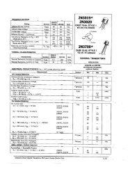
ABSOLUTE MAXIMUM RATINGS<br />
Symbol Parameter Value Unit<br />
VCC Power Supply Voltage 50 V<br />
VIR Comparator Input Voltage Range -0.3 to 40 V<br />
VSWC Switch Collector Voltage 40 V<br />
VSWE Switch Emitter Voltage (VSWC =40V) 40 V<br />
VCE Switch Collector to Emitter Voltage 40 V<br />
VDC Driver Collector Voltage 40 V<br />
IDC Driver Collector Current 100 mA<br />
ISW Switch Current 1.5 A<br />
PTOT Power Dissipation at TA = 25°C for DIP-8<br />
for SO-8<br />
1.25<br />
0.625<br />
W<br />
TJ Operating Junction Temperature 150 °C<br />
TSTG Storage Temperature Range -40 to 150 °C<br />
Operating Ambient Temperature Range for AC and EC SERIES 0 to 70<br />
TOP for AB SERIES -40 to 85<br />
°C<br />
for EB SERIES -40 to 125<br />
Absolute Maximum Ratings are those values beyond which damage to the device may occur. Functional operation under these condition is<br />
not implied.<br />
THERMAL DATA<br />
Symbol Parameter DIP-8 SO-8 Unit<br />
Rthj-amb Thermal Resistance Junction-ambient (*) 100 160 °C/W<br />
Rthj-case Thermal Resistance Junction-case 42 20 °C/W<br />
(*) This value depends from thermal design of PCB on which the device is mounted.<br />
CONNECTION DIAGRAM (top view)<br />
PIN DESCRIPTION<br />
2/16<br />
Pin N° Symbol Name and Function<br />
1 SWC Switch Collector<br />
2 SWE Switch Emitter<br />
3 TC Timing Capacitor<br />
4 GND Ground<br />
5 CII Comparator Inverting Input<br />
6 VCC Voltage Supply<br />
7 IPK IPK Sense<br />
8 DRC Voltage Driver Collector