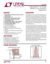
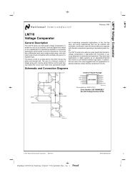
LP2950/LP2951 Series of Adjustable Micropower Voltage Regulators
LP2950/LP2951 Series of Adjustable Micropower Voltage Regulators
LP2950/LP2951 Series of Adjustable Micropower Voltage Regulators

Create successful ePaper yourself
Turn your PDF publications into a flip-book with our unique Google optimized e-Paper software.
<strong>LP2950</strong>/<strong>LP2951</strong><br />
<strong>Series</strong> <strong>of</strong> <strong>Adjustable</strong> <strong>Micropower</strong> <strong>Voltage</strong> <strong>Regulators</strong><br />
General Description<br />
The <strong>LP2950</strong> and <strong>LP2951</strong> are micropower voltage regulators<br />
with very low quiescent current (75 µA typ.) and very low<br />
dropout voltage (typ. 40 mV at light loads and 380 mV at<br />
100 mA). They are ideally suited for use in battery-powered<br />
systems. Furthermore, the quiescent current <strong>of</strong> the <strong>LP2950</strong>/<br />
<strong>LP2951</strong> increases only slightly in dropout, prolonging battery<br />
life.<br />
The <strong>LP2950</strong>-5.0 is available in the surface-mount D-Pak<br />
package, and in the popular 3-pin TO-92 package for<br />
pin-compatibility with older 5V regulators. The 8-lead<br />
<strong>LP2951</strong> is available in plastic, ceramic dual-in-line, or metal<br />
can packages and <strong>of</strong>fers additional system functions.<br />
One such feature is an error flag output which warns <strong>of</strong> a low<br />
output voltage, <strong>of</strong>ten due to falling batteries on the input. It<br />
may be used for a power-on reset. A second feature is the<br />
logic-compatible shutdown input which enables the regulator<br />
to be switched on and <strong>of</strong>f. Also, the part may be pin-strapped<br />
for a 5V, 3V, or 3.3V output (depending on the version), or<br />
programmed from 1.24V to 29V with an external pair <strong>of</strong> resistors.<br />
Careful design <strong>of</strong> the <strong>LP2950</strong>/<strong>LP2951</strong> has minimized all contributions<br />
to the error budget. This includes a tight initial tolerance<br />
(.5% typ.), extremely good load and line regulation<br />
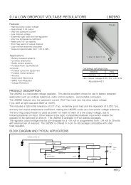
Block Diagram and Typical Applications<br />
<strong>LP2950</strong><br />
DS008546-25<br />
(.05% typ.) and a very low output voltage temperature coefficient,<br />
making the part useful as a low-power voltage reference.<br />
Features<br />
n 5V, 3V, and 3.3V versions available<br />
n High accuracy output voltage<br />
n Guaranteed 100 mA output current<br />
n Extremely low quiescent current<br />
n Low dropout voltage<br />
n Extremely tight load and line regulation<br />
n Very low temperature coefficient<br />
n Use as Regulator or Reference<br />
n Needs minimum capacitance for stability<br />
n Current and Thermal Limiting<br />
n Stable with low-ESR output capacitors<br />
<strong>LP2951</strong> versions only<br />
n Error flag warns <strong>of</strong> output dropout<br />
n Logic-controlled electronic shutdown<br />
n Output programmable from 1.24 to 29V<br />
<strong>LP2951</strong><br />
July 2000<br />
DS008546-1<br />
© 2000 National Semiconductor Corporation DS008546 www.national.com<br />
<strong>LP2950</strong>/<strong>LP2951</strong> <strong>Series</strong> <strong>of</strong> <strong>Adjustable</strong> <strong>Micropower</strong> <strong>Voltage</strong> <strong>Regulators</strong>
<strong>LP2950</strong>/<strong>LP2951</strong><br />
Connection Diagrams<br />
TO-92 Plastic Package (Z)<br />
Bottom View<br />
DS008546-2<br />
Metal Can Package (H)<br />
Top View<br />
TO-252 (D-Pak)<br />
Front View<br />
DS008546-19<br />
DS008546-70<br />
www.national.com 2<br />
Dual-In-Line Packages (N, J)<br />
Surface-Mount Package (M, MM)<br />
Top View<br />
DS008546-26<br />
10-Lead Ceramic Surface-Mount Package (WG)<br />
Top View<br />
DS008546-64
Ordering Information<br />
Package Output <strong>Voltage</strong> Temperature<br />
3.0V 3.3V 5.0V (˚C)<br />
TO-92 (Z) <strong>LP2950</strong>ACZ-3.0 <strong>LP2950</strong>ACZ-3.3 <strong>LP2950</strong>ACZ-5.0 −40 < TJ < 125<br />
<strong>LP2950</strong>CZ-3.0 <strong>LP2950</strong>CZ-3.3 <strong>LP2950</strong>CZ-5.0<br />
TO-252 (D-Pak) <strong>LP2950</strong>CDT-3.0 <strong>LP2950</strong>CDT-3.3 <strong>LP2950</strong>CDT-5.0 −40 < TJ < 125<br />
N (N-08E) <strong>LP2951</strong>ACN-3.0 <strong>LP2951</strong>ACN-3.3 <strong>LP2951</strong>ACN −40 < TJ < 125<br />
<strong>LP2951</strong>CN-3.0 <strong>LP2951</strong>CN-3.3 <strong>LP2951</strong>CN<br />
M (M08A) <strong>LP2951</strong>ACM-3.0 <strong>LP2951</strong>ACM-3.3 <strong>LP2951</strong>ACM −40 < TJ < 125<br />
<strong>LP2951</strong>CM-3.0 <strong>LP2951</strong>CM-3.3 <strong>LP2951</strong>CM<br />
MM (MUA08A) in<br />
Tape and Reel<br />
<strong>LP2951</strong>ACMM-3.0 <strong>LP2951</strong>ACMM-3.3 <strong>LP2951</strong>ACMM −40 < TJ < 125<br />
<strong>LP2951</strong>CMM-3.0 <strong>LP2951</strong>CMM-3.3 <strong>LP2951</strong>CMM<br />
J (J08A) <strong>LP2951</strong>ACJ<br />
<strong>LP2951</strong>CJ<br />
−40 < TJ < 125<br />
<strong>LP2951</strong>J<br />
<strong>LP2951</strong>J/883<br />
5926-3870501MPA<br />
−55 < TJ < 150<br />
H (H08C) <strong>LP2951</strong>H/883<br />
5962-3870501MGA<br />
−55 < TJ < 150<br />
WG (WG10A) <strong>LP2951</strong>WG/883<br />
5962-3870501MXA<br />
−55 < TJ < 150<br />
Package Marking for MM Package:<br />
Order Number Package Marking<br />
<strong>LP2951</strong>ACMM L0DA<br />
<strong>LP2951</strong>CMM L0DB<br />
<strong>LP2951</strong>ACMM-3.3 L0CA<br />
<strong>LP2951</strong>CMM-3.3 L0CB<br />
<strong>LP2951</strong>ACMM-3.0 L0BA<br />
<strong>LP2951</strong>CMM-3.0 L0BB<br />
3<br />
www.national.com<br />
<strong>LP2950</strong>/<strong>LP2951</strong>
<strong>LP2950</strong>/<strong>LP2951</strong><br />
Absolute Maximum Ratings (Note 1)<br />
If Military/Aerospace specified devices are required,<br />
please contact the National Semiconductor Sales Office/<br />
Distributors for availability and specifications.<br />
Input Supply <strong>Voltage</strong> −0.3 to +30V<br />
SHUTDOWN Input <strong>Voltage</strong>,<br />
Error Comparator Output<br />
<strong>Voltage</strong>, (Note 9)<br />
FEEDBACK Input <strong>Voltage</strong> −1.5 to +30V<br />
(Note 9) (Note 10)<br />
Power Dissipation Internally Limited<br />
Junction Temperature (T J) +150˚C<br />
Ambient Storage Temperature −65˚ to +150˚C<br />
Soldering Dwell Time, Temperature<br />
Wave<br />
Infrared<br />
Vapor Phase<br />
4 seconds, 260˚C<br />
10 seconds, 240˚C<br />
75 seconds, 219˚C<br />
ESD TBD<br />
Operating Ratings (Note 1)<br />
Maximum Input Supply <strong>Voltage</strong> 30V<br />
Junction Temperature Range<br />
(T J) (Note 8)<br />
<strong>LP2951</strong> −55˚ to +150˚C<br />
<strong>LP2950</strong>AC-XX, <strong>LP2950</strong>C-XX,<br />
<strong>LP2951</strong>AC-XX, <strong>LP2951</strong>C-XX −40˚ to +125˚C<br />
Electrical Characteristics (Note 2)<br />
<strong>LP2951</strong> <strong>LP2950</strong>AC-XX <strong>LP2950</strong>C-XX<br />
Parameter<br />
Conditions<br />
(Note 2)<br />
Typ<br />
Tested<br />
Limit Typ<br />
<strong>LP2951</strong>AC-XX<br />
Tested Design<br />
Limit Limit Typ<br />
<strong>LP2951</strong>C-XX<br />
Tested Design<br />
Limit Limit<br />
Units<br />
(Notes 3, 16) (Note 3) (Note 4) (Note 3) (Note 4)<br />
3V VERSIONS (Note 17)<br />
Output <strong>Voltage</strong> TJ = 25˚C 3.0 3.015 3.0 3.015 3.0 3.030 V max<br />
2.985 2.985 2.970 V min<br />
−25˚C ≤ TJ ≤ 85˚C 3.0 3.0 3.030 3.0 3.045 V max<br />
2.970 2.955 V min<br />
Full Operating 3.0 3.036 3.0 3.036 3.0 3.060 V max<br />
Temperature Range 2.964 2.964 2.940 V min<br />
Output <strong>Voltage</strong> 100 µA ≤ IL ≤ 100 mA 3.0 3.045 3.0 3.042 3.0 3.072 V max<br />
3.3V VERSIONS (Note 17)<br />
TJ ≤ TJMAX 2.955 2.958 2.928 V min<br />
Output <strong>Voltage</strong> TJ = 25˚C 3.3 3.317 3.3 3.317 3.3 3.333 V max<br />
3.284 3.284 3.267 V min<br />
−25˚C ≤ TJ ≤ 85˚C 3.3 3.3 3.333 3.3 3.350 V max<br />
3.267 3.251 V min<br />
Full Operating 3.3 3.340 3.3 3.340 3.3 3.366 V max<br />
Temperature Range 3.260 3.260 3.234 V min<br />
Output <strong>Voltage</strong> 100 µA ≤ IL ≤ 100 mA 3.3 3.350 3.3 3.346 3.3 3.379 V max<br />
5V VERSIONS (Note 17)<br />
TJ ≤ TJMAX 3.251 3.254 3.221 V min<br />
Output <strong>Voltage</strong> TJ = 25˚C 5.0 5.025 5.0 5.025 5.0 5.05 V max<br />
4.975 4.975 4.95 V min<br />
−25˚C ≤ TJ ≤ 85˚C 5.0 5.0 5.05 5.0 5.075 V max<br />
4.95 4.925 V min<br />
Full Operating 5.0 5.06 5.0 5.06 5.0 5.1 V max<br />
Temperature Range 4.94 4.94 4.9 V min<br />
Output <strong>Voltage</strong> 100 µA ≤ IL ≤ 100 mA 5.0 5.075 5.0 5.075 5.0 5.12 V max<br />
ALL VOLTAGE OPTIONS<br />
TJ ≤ TJMAX 4.925 4.925 4.88 V min<br />
Output <strong>Voltage</strong><br />
Temperature Coefficient<br />
(Note 12) 20 120 20 100 50 150 ppm/˚C<br />
Line Regulation<br />
(Note 14)<br />
(VONOM + 1)V ≤ Vin ≤ 30V<br />
(Note 15)<br />
0.03 0.1<br />
0.5<br />
0.03 0.1<br />
0.2<br />
0.04 0.2<br />
0.4<br />
% max<br />
% max<br />
Load Regulation<br />
(Note 14)<br />
100 µA ≤ IL ≤ 100 mA 0.04 0.1<br />
0.3<br />
0.04 0.1<br />
0.2<br />
0.1 0.2<br />
0.3<br />
% max<br />
% max<br />
www.national.com 4
Electrical Characteristics (Note 2) (Continued)<br />
<strong>LP2951</strong> <strong>LP2950</strong>AC-XX <strong>LP2950</strong>C-XX<br />
Parameter<br />
Conditions<br />
(Note 2)<br />
Typ<br />
Tested<br />
Limit Typ<br />
<strong>LP2951</strong>AC-XX<br />
Tested Design<br />
Limit Limit Typ<br />
<strong>LP2951</strong>C-XX<br />
Tested Design<br />
Limit Limit<br />
Units<br />
(Notes 3, 16) (Note 3) (Note 4) (Note 3) (Note 4)<br />
ALL VOLTAGE OPTIONS<br />
Dropout <strong>Voltage</strong><br />
(Note 5)<br />
IL = 100 µA<br />
50<br />
80<br />
150 50<br />
80<br />
150 50<br />
80<br />
150<br />
mV max<br />
mV max<br />
IL = 100 mA 450 450 450 mV max<br />
380 600 380 600 380 600 mV max<br />
Ground IL = 100 µA 75 120 75 120 75 120 µA max<br />
Current 140 140 140 µA max<br />
IL = 100 mA 8 12 8 12 8 12 mA max<br />
14 14 14 mA max<br />
Dropout Vin =(VONOM − 0.5)V 110 170 110 170 110 170 µA max<br />
Ground Current IL = 100 µA 200 200 200 µA max<br />
Current Limit Vout = 0 160 200 160 200 160 200 mA max<br />
220 220 220 mA max<br />
Thermal Regulation (Note 13) 0.05 0.2 0.05 0.2 0.05 0.2 %/W max<br />
Output Noise, CL = 1 µF (5V Only) 430 430 430 µV rms<br />
10 Hz to 100 kHz CL = 200 µF<br />
CL = 3.3 µF<br />
160 160 160 µV rms<br />
(Bypass = 0.01 µF<br />
Pins 7 to 1 (<strong>LP2951</strong>))<br />
100 100 100 µV rms<br />
8-PIN VERSIONS ONLY <strong>LP2951</strong> <strong>LP2951</strong>AC-XX <strong>LP2951</strong>C-XX<br />
Reference 1.235 1.25 1.235 1.25 1.235 1.26 V max<br />
<strong>Voltage</strong> 1.26 1.26 1.27 V max<br />
1.22 1.22 1.21 V min<br />
1.2 1.2 1.2 V min<br />
Reference (Note 7) 1.27 1.27 1.285 V max<br />
<strong>Voltage</strong> 1.19 1.19 1.185 V min<br />
Feedback Pin 20 40 20 40 20 40 nA max<br />
Bias Current 60 60 60 nA max<br />
Reference <strong>Voltage</strong><br />
Temperature Coefficient<br />
(Note 12) 20 20 50 ppm/˚C<br />
Feedback Pin Bias<br />
Current Temperature<br />
Coefficient<br />
Error Comparator<br />
0.1 0.1 0.1 nA/˚C<br />
Output Leakage VOH = 30V 0.01 1 0.01 1 0.01 1 µA max<br />
Current 2 2 2 µA max<br />
Output Low Vin =(VONOM − 0.5)V 150 250 150 250 150 250 mV max<br />
<strong>Voltage</strong> IOL = 400 µA 400 400 400 mV max<br />
Upper Threshold (Note 6) 60 40 60 40 60 40 mV min<br />
<strong>Voltage</strong> 25 25 25 mV min<br />
Lower Threshold (Note 6) 75 95 75 95 75 95 mV max<br />
<strong>Voltage</strong> 140 140 140 mV max<br />
Hysteresis<br />
Shutdown Input<br />
(Note 6) 15 15 15 mV<br />
Input 1.3 1.3 1.3 V<br />
Logic Low (Regulator ON) 0.6 0.7 0.7 V max<br />
<strong>Voltage</strong> High (Regulator OFF) 2.0 2.0 2.0 V min<br />
5<br />
www.national.com<br />
<strong>LP2950</strong>/<strong>LP2951</strong>
<strong>LP2950</strong>/<strong>LP2951</strong><br />
Electrical Characteristics (Note 2) (Continued)<br />
Parameter<br />
Shutdown Input<br />
Shutdown Pin Input<br />
Current<br />
Regulator Output<br />
Current in Shutdown<br />
Conditions<br />
(Note 2)<br />
<strong>LP2951</strong> <strong>LP2950</strong>AC-XX <strong>LP2950</strong>C-XX<br />
<strong>LP2951</strong>AC-XX <strong>LP2951</strong>C-XX<br />
Tested Tested Design Tested Design<br />
Typ Limit Typ Limit Limit Typ Limit Limit<br />
(Notes 3, 16) (Note 3) (Note 4) (Note 3) (Note 4)<br />
Vshutdown = 2.4V 30 50 30 50 30 50 µA max<br />
100 100 100 µA max<br />
Vshutdown = 30V 450 600 450 600 450 600 µA max<br />
750 750 750 µA max<br />
(Note 11) 3 10 3 10 3 10 µA max<br />
20 20 20 µA max<br />
Note 1: Absolute Maximum Ratings are limits beyond which damage to the device may occur. Operating Ratings are conditions under which operation <strong>of</strong> the device<br />
is guaranteed. Operating Ratings do not imply guaranteed performance limits. For guaranteed performance limits and associated test conditions, see the Electrical<br />
Characteristics tables.<br />
Note 2: Unless otherwise specified all limits guaranteed for VIN =(VONOM + 1)V, IL = 100 µA and CL = 1 µF for 5V versions and 2.2 µF for 3V and 3.3V versions.<br />
Limits appearing in boldface type apply over the entire junction temperature range for operation. Limits appearing in normal type apply for TA =TJ= 25˚C. Additional<br />
conditions for the 8-pin versions are FEEDBACK tied to VTAP, OUTPUT tied to SENSE, and VSHUTDOWN ≤ 0.8V.<br />
Note 3: Guaranteed and 100% production tested.<br />
Note 4: Guaranteed but not 100% production tested. These limits are not used to calculate outgoing AQL levels.<br />
Note 5: Dropout <strong>Voltage</strong> is defined as the input to output differential at which the output voltage drops 100 mV below its nominal value measured at 1V differential.<br />
At very low values <strong>of</strong> programmed output voltage, the minimum input supply voltage <strong>of</strong> 2V (2.3V over temperature) must be taken into account.<br />
Note 6: Comparator thresholds are expressed in terms <strong>of</strong> a voltage differential at the Feedback terminal below the nominal reference voltage measured at<br />
Vin =(VONOM + 1)V. To express these thresholds in terms <strong>of</strong> output voltage change, multiply by the error amplifier gain = Vout/Vref = (R1 + R2)/R2.<br />
For example, at a programmed output voltage <strong>of</strong> 5V, the Error output is guaranteed to go low when the output drops by 95 mV x 5V/1.235V = 384 mV.<br />
Thresholds remain constant as a percent <strong>of</strong> Vout as Vout is varied, with the dropout warning occurring at typically 5% below nominal, 7.5% guaranteed.<br />
Note 7: Vref ≤ Vout ≤ (Vin − 1V), 2.3V ≤ Vin ≤ 30V, 100 µA ≤ IL ≤ 100 mA, TJ ≤ TJMAX. Note 8: The junction-to-ambient thermal resistances are as follows: 180˚C/W and 160˚C/W for the TO-92 package with 0.40 inch and 0.25 inch leads to the printe d<br />
circuit board (PCB) respectively, 105˚C/W for the molded plastic DIP (N), 130˚C/W for the ceramic DIP (J), 160˚C/W for the molded plastic SOP (M), 200˚ C/W for the<br />
molded plastic MSOP (MM), and 160˚C/W for the metal can package (H). The above thermal resistances for the N, J, M, and MM packages apply when the package<br />
is soldered directly to the PCB. Junction-to-case thermal resistance for the H package is 20˚C/W. Junction-to-case thermal resistance for the TO-25 2 package is<br />
5.4˚C/W.<br />
Note 9: May exceed input supply voltage.<br />
Note 10: When used in dual-supply systems where the output terminal sees loads returned to a negative supply, the output voltage should be diode-clamped to<br />
ground.<br />
Note 11: Vshutdown ≥ 2V, Vin ≤ 30V, Vout = 0, Feedback pin tied to VTAP. Note 12: Output or reference voltage temperature coefficient is defined as the worst case voltage change divided by the total temperature range.<br />
Note 13: Thermal regulation is defined as the change in output voltage at a time T after a change in power dissipation is applied, excluding load or line regulation<br />
effects. Specifications are for a 50 mA load pulse at VIN = 30V (1.25W pulse) for T = 10 ms.<br />
Note 14: Regulation is measured at constant junction temperature, using pulse testing with a low duty cycle. Changes in output voltage due to heating effects are<br />
covered under the specification for thermal regulation.<br />
Note 15: Line regulation for the <strong>LP2951</strong> is tested at 150˚C for I L = 1 mA. For IL = 100 µA and TJ = 125˚C, line regulation is guaranteed by design to 0.2%. See Typical<br />
Performance Characteristics for line regulation versus temperature and load current.<br />
Note 16: A Military RETS specification is available on request. At time <strong>of</strong> printing, the <strong>LP2951</strong> RETS specification complied with the boldface limits in this column.<br />
The <strong>LP2951</strong>H, WG, or J may also be procured as Standard Military Drawing Spec #5962-3870501MGA, MXA, or MPA.<br />
Note 17: All <strong>LP2950</strong> devices have the nominal output voltage coded as the last two digits <strong>of</strong> the part number. In the <strong>LP2951</strong> products, the 3.0V and 3.3V versions<br />
are designated by the last two digits, but the 5V version is denoted with no code at this location <strong>of</strong> the part number (refer to ordering information table).<br />
Typical Performance Characteristics<br />
Quiescent Current<br />
DS008546-27<br />
Dropout Characteristics<br />
www.national.com 6<br />
DS008546-28<br />
Input Current<br />
DS008546-29<br />
Units
Typical Performance Characteristics (Continued)<br />
Input Current<br />
Quiescent Current<br />
Short Circuit Current<br />
DS008546-30<br />
DS008546-33<br />
DS008546-36<br />
Output <strong>Voltage</strong> vs.<br />
Temperature <strong>of</strong> 3<br />
Representative Units<br />
Quiescent Current<br />
Dropout <strong>Voltage</strong><br />
7<br />
DS008546-31<br />
DS008546-34<br />
DS008546-37<br />
Quiescent Current<br />
Quiescent Current<br />
Dropout <strong>Voltage</strong><br />
DS008546-32<br />
DS008546-35<br />
DS008546-38<br />
www.national.com<br />
<strong>LP2950</strong>/<strong>LP2951</strong>
<strong>LP2950</strong>/<strong>LP2951</strong><br />
Typical Performance Characteristics (Continued)<br />
<strong>LP2951</strong><br />
Minimum Operating <strong>Voltage</strong><br />
<strong>LP2951</strong><br />
Error Comparator Output<br />
Load Transient Response<br />
DS008546-39<br />
DS008546-42<br />
DS008546-45<br />
<strong>LP2951</strong><br />
Feedback Bias Current<br />
<strong>LP2951</strong><br />
Comparator Sink Current<br />
Load Transient Response<br />
www.national.com 8<br />
DS008546-40<br />
DS008546-43<br />
DS008546-46<br />
<strong>LP2951</strong><br />
Feedback Pin Current<br />
Line Transient Response<br />
<strong>LP2951</strong><br />
Enable Transient<br />
DS008546-41<br />
DS008546-44<br />
DS008546-47
Typical Performance Characteristics (Continued)<br />
Output Impedance<br />
Ripple Rejection<br />
Shutdown Threshold <strong>Voltage</strong><br />
<strong>LP2950</strong> Maximum<br />
Rated Output Current<br />
DS008546-48<br />
DS008546-51<br />
DS008546-54<br />
DS008546-57<br />
Ripple Rejection<br />
<strong>LP2951</strong> Output Noise<br />
Line Regulation<br />
Thermal Response<br />
9<br />
DS008546-49<br />
DS008546-52<br />
DS008546-55<br />
DS008546-58<br />
Ripple Rejection<br />
<strong>LP2951</strong> Divider Resistance<br />
<strong>LP2951</strong> Maximum<br />
Rated Output Current<br />
Output Capacitor ESR Range<br />
DS008546-50<br />
DS008546-53<br />
DS008546-56<br />
DS008546-63<br />
www.national.com<br />
<strong>LP2950</strong>/<strong>LP2951</strong>
<strong>LP2950</strong>/<strong>LP2951</strong><br />
Application Hints<br />
EXTERNAL CAPACITORS<br />
A 1.0 µF (or greater) capacitor is required between the output<br />
and ground for stability at output voltages <strong>of</strong> 5V or more.<br />
At lower output voltages, more capacitance is required<br />
(2.2 µF or more is recommended for 3V and 3.3V versions).<br />
Without this capacitor the part will oscillate. Most types <strong>of</strong><br />
tantalum or aluminum electrolytics work fine here; even film<br />
types work but are not recommended for reasons <strong>of</strong> cost.<br />
Many aluminum electrolytics have electrolytes that freeze at<br />
about −30˚C, so solid tantalums are recommended for operation<br />
below −25˚C. The important parameters <strong>of</strong> the capacitor<br />
are an ESR <strong>of</strong> about 5 Ω or less and a resonant frequency<br />
above 500 kHz. The value <strong>of</strong> this capacitor may be<br />
increased without limit.<br />
At lower values <strong>of</strong> output current, less output capacitance is<br />
required for stability. The capacitor can be reduced to<br />
0.33 µF for currents below 10 mA or 0.1 µF for currents below<br />
1 mA. Using the adjustable versions at voltages below<br />
5V runs the error amplifier at lower gains so that more output<br />
capacitance is needed. For the worst-case situation <strong>of</strong> a<br />
100 mA load at 1.23V output (Output shorted to Feedback) a<br />
3.3 µF (or greater) capacitor should be used.<br />
Unlike many other regulators, the <strong>LP2950</strong> will remain stable<br />
and in regulation with no load in addition to the internal voltage<br />
divider. This is especially important in CMOS RAM<br />
keep-alive applications. When setting the output voltage <strong>of</strong><br />
the <strong>LP2951</strong> versions with external resistors, a minimum load<br />
<strong>of</strong> 1 µA is recommended.<br />
A 1 µF tantalum or aluminum electrolytic capacitor should be<br />
placed from the <strong>LP2950</strong>/<strong>LP2951</strong> input to ground if there is<br />
more than 10 inches <strong>of</strong> wire between the input and the AC filter<br />
capacitor or if a battery is used as the input.<br />
Stray capacitance to the <strong>LP2951</strong> Feedback terminal can<br />
cause instability. This may especially be a problem when using<br />
high value external resistors to set the output voltage.<br />
Adding a 100 pF capacitor between Output and Feedback<br />
and increasing the output capacitor to at least 3.3 µF will fix<br />
this problem.<br />
ERROR DETECTION COMPARATOR OUTPUT<br />
The comparator produces a logic low output whenever the<br />
<strong>LP2951</strong> output falls out <strong>of</strong> regulation by more than approximately<br />
5%. This figure is the comparator’s built-in <strong>of</strong>fset <strong>of</strong><br />
about 60 mV divided by the 1.235 reference voltage. (Refer<br />
to the block diagram in the front <strong>of</strong> the datasheet.) This trip<br />
level remains “5% below normal” regardless <strong>of</strong> the programmed<br />
output voltage <strong>of</strong> the 2951. For example, the error<br />
flag trip level is typically 4.75V for a 5V output or 11.4V for a<br />
12V output. The out <strong>of</strong> regulation condition may be due either<br />
to low input voltage, current limiting, or thermal limiting.<br />
Figure 1 below gives a timing diagram depicting the ERROR<br />
signal and the regulated output voltage as the <strong>LP2951</strong> input<br />
is ramped up and down. For 5V versions, the ERROR signal<br />
becomes valid (low) at about 1.3V input. It goes high at<br />
about 5V input (the input voltage at which VOUT = 4.75V).<br />
Since the <strong>LP2951</strong>’s dropout voltage is load-dependent (see<br />
curve in typical performance characteristics), the input voltage<br />
trip point (about 5V) will vary with the load current. The<br />
output voltage trip point (approx. 4.75V) does not vary with<br />
load.<br />
The error comparator has an open-collector output which requires<br />
an external pullup resistor. This resistor may be returned<br />
to the output or some other supply voltage depending<br />
on system requirements. In determining a value for this re-<br />
www.national.com 10<br />
sistor, note that while the output is rated to sink 400 µA, this<br />
sink current adds to battery drain in a low battery condition.<br />
Suggested values range from 100k to 1 MΩ. The resistor is<br />
not required if this output is unused.<br />
DS008546-20<br />
*When VIN ≤ 1.3V, the error flag pin becomes a high impedance, and the<br />
error flag voltage rises to its pull-up voltage. Using VOUT as the pull-up<br />
voltage (see Figure 2), rather than an external 5V source, will keep the<br />
error flag voltage under 1.2V (typ.) in this condition. The user may wish to<br />
divide down the error flag voltage using equal-value resistors (10 kΩ<br />
suggested), to ensure a low-level logic signal during any fault condition,<br />
while still allowing a valid high logic level during normal operation.<br />
FIGURE 1. ERROR Output Timing<br />
PROGRAMMING THE OUTPUT VOLTAGE (<strong>LP2951</strong>)<br />
The <strong>LP2951</strong> may be pin-strapped for the nominal fixed output<br />
voltage using its internal voltage divider by tying the output<br />
and sense pins together, and also tying the feedback and<br />
VTAP pins together. Alternatively, it may be programmed for<br />
any output voltage between its 1.235V reference and its 30V<br />
maximum rating. As seen in Figure 2, an external pair <strong>of</strong> resistors<br />
is required.<br />
The complete equation for the output voltage is<br />
where V REF is the nominal 1.235 reference voltage and I FB is<br />
the feedback pin bias current, nominally −20 nA. The minimum<br />
recommended load current <strong>of</strong> 1 µA forces an upper<br />
limit <strong>of</strong> 1.2 MΩ on the value <strong>of</strong> R 2, if the regulator must work<br />
with no load (a condition <strong>of</strong>ten found in CMOS in standby).<br />
I FB will produce a 2% typical error in V OUT which may be<br />
eliminated at room temperature by trimming R 1. For better<br />
accuracy, choosing R 2 = 100k reduces this error to 0.17%<br />
while increasing the resistor program current to 12 µA. Since<br />
the <strong>LP2951</strong> typically draws 60 µA at no load with Pin 2<br />
open-circuited, this is a small price to pay.
Application Hints (Continued)<br />
*See Application Hints<br />
DS008546-7<br />
**Drive with TTL-high to shut down. Ground or leave open if shutdown<br />
feature is not to be used.<br />
Note: Pins 2 and 6 are left open.<br />
FIGURE 2. <strong>Adjustable</strong> Regulator<br />
REDUCING OUTPUT NOISE<br />
In reference applications it may be advantageous to reduce<br />
the AC noise present at the output. One method is to reduce<br />
the regulator bandwidth by increasing the size <strong>of</strong> the output<br />
capacitor. This is the only way noise can be reduced on the<br />
3 lead <strong>LP2950</strong> but is relatively inefficient, as increasing the<br />
capacitor from 1 µF to 220 µF only decreases the noise from<br />
430 µV to 160 µV rms for a 100 kHz bandwidth at 5V output.<br />
Noise can be reduced fourfold by a bypass capacitor across<br />
R1, since it reduces the high frequency gain from 4 to unity.<br />
Pick<br />
or about 0.01 µF. When doing this, the output capacitor must<br />
be increased to 3.3 µF to maintain stability. These changes<br />
reduce the output noise from 430 µV to 100 µV rms for a<br />
100 kHz bandwidth at 5V output. With the bypass capacitor<br />
added, noise no longer scales with output voltage so that improvements<br />
are more dramatic at higher output voltages.<br />
11<br />
www.national.com<br />
<strong>LP2950</strong>/<strong>LP2951</strong>
<strong>LP2950</strong>/<strong>LP2951</strong><br />
Typical Applications<br />
300 mA Regulator with 0.75V Dropout<br />
Low Drift Current Source<br />
1A Regulator with 1.2V Dropout<br />
DS008546-8<br />
www.national.com 12<br />
DS008546-22<br />
Wide Input <strong>Voltage</strong> Range Current Limiter<br />
DS008546-9<br />
DS008546-21<br />
*Minimum input-output voltage ranges from 40 mV to 400 mV, depending<br />
on load current. Current limit is typically 160 mA.<br />
5 Volt Current Limiter<br />
DS008546-10<br />
*Minimum input-output voltage ranges from 40 mV to 400 mV, depending<br />
on load current. Current limit is typically 160 mA.
Typical Applications (Continued)<br />
Regulator with Early Warning and Auxiliary Output<br />
DS008546-11<br />
j Early warning flag on low input voltage<br />
j Main output latches <strong>of</strong>f at lower input voltages<br />
j Battery backup on auxiliary output<br />
Operation: Reg. #1’s V out is programmed one diode drop above 5V. Its<br />
error flag becomes active when V in ≤ 5.7V. When V in drops below 5.3V,<br />
the error flag <strong>of</strong> Reg. #2 becomes active and via Q1 latches the main<br />
output <strong>of</strong>f. When V in again exceeds 5.7V Reg. #1 is back in regulation and<br />
the early warning signal rises, unlatching Reg. #2 via D3.<br />
13<br />
Latch Off When Error Flag Occurs<br />
DS008546-12<br />
www.national.com<br />
<strong>LP2950</strong>/<strong>LP2951</strong>
<strong>LP2950</strong>/<strong>LP2951</strong><br />
Typical Applications (Continued)<br />
For 5V out, use internal resistors. Wire pin 6 to 7, & wire pin 2 to +V out Bus.<br />
5V Regulator with 2.5V Sleep Function<br />
*High input lowers V out to 2.5V<br />
2 Ampere Low Dropout Regulator<br />
DS008546-14<br />
www.national.com 14<br />
DS008546-13<br />
Open Circuit Detector for 4 → 20 mA Current Loop<br />
DS008546-15
Typical Applications (Continued)<br />
Regulator with State-<strong>of</strong>-Charge Indicator<br />
*Optional Latch <strong>of</strong>f when drop out occurs. Adjust R3 for C2 Switching when V in is 6.0V.<br />
**Outputs go low when V in drops below designated thresholds.<br />
Low Battery Disconnect<br />
DS008546-16<br />
For values shown, Regulator shuts down when V in < 5.5V and turns on again at 6.0V. Current drain in disconnected mode is ≈ 150 µA.<br />
*Sets disconnect <strong>Voltage</strong><br />
**Sets disconnect Hysteresis<br />
15<br />
DS008546-17<br />
www.national.com<br />
<strong>LP2950</strong>/<strong>LP2951</strong>
<strong>LP2950</strong>/<strong>LP2951</strong><br />
Typical Applications (Continued)<br />
LM34 for 125˚F Shutdown<br />
LM35 for 125˚C Shutdown<br />
System Overtemperature Protection Circuit<br />
www.national.com 16<br />
DS008546-18
Schematic Diagram<br />
17<br />
DS008546-23<br />
www.national.com<br />
<strong>LP2950</strong>/<strong>LP2951</strong>
<strong>LP2950</strong>/<strong>LP2951</strong><br />
Physical Dimensions inches (millimeters) unless otherwise noted<br />
Order Number <strong>LP2951</strong>WG/883 or 5962-3870501MXA<br />
NS Package Number WG10A<br />
Metal Can Package (H)<br />
Order Number <strong>LP2951</strong>H/883 or 5962-3870501MGA<br />
NS Package Number H08C<br />
www.national.com 18
Physical Dimensions inches (millimeters) unless otherwise noted (Continued)<br />
Ceramic Dual-In-Line Package (J)<br />
Order Number <strong>LP2951</strong>CJ, <strong>LP2951</strong>ACJ, <strong>LP2951</strong>J, <strong>LP2951</strong>J/883 or 5962-3870501MPA<br />
NS Package Number J08A<br />
Surface Mount Package (M)<br />
Order Number <strong>LP2951</strong>ACM, <strong>LP2951</strong>CM, <strong>LP2951</strong>ACM-3.0,<br />
<strong>LP2951</strong>CM-3.0, <strong>LP2951</strong>ACM-3.3 or <strong>LP2951</strong>CM-3.3<br />
NS Package Number M08A<br />
19<br />
www.national.com<br />
<strong>LP2950</strong>/<strong>LP2951</strong>
<strong>LP2950</strong>/<strong>LP2951</strong><br />
Physical Dimensions inches (millimeters) unless otherwise noted (Continued)<br />
Molded Dual-In-Line Package (N)<br />
Order Number <strong>LP2951</strong>ACN, <strong>LP2951</strong>CN, <strong>LP2951</strong>ACN-3.0,<br />
<strong>LP2951</strong>CN-3.0, or <strong>LP2951</strong>ACN-3.3 or <strong>LP2951</strong>CN-3.3<br />
NS Package Number N08E<br />
Molded TO-92 Package (Z)<br />
Order Number <strong>LP2950</strong>ACZ-3.0 or <strong>LP2950</strong>CZ-3.0, <strong>LP2950</strong>ACZ-3.3,<br />
<strong>LP2950</strong>CZ-3.3, <strong>LP2950</strong>ACZ-5.0 or <strong>LP2950</strong>CZ-5.0<br />
NS Package Number Z03A<br />
www.national.com 20
Physical Dimensions inches (millimeters) unless otherwise noted (Continued)<br />
Surface Mount Package (MM)<br />
Order Number <strong>LP2951</strong>ACMM, <strong>LP2951</strong>CMM, <strong>LP2951</strong>ACMM-3.0,<br />
<strong>LP2951</strong>CMM-3.0, <strong>LP2951</strong>ACMM-3.3 or <strong>LP2951</strong>CMM-3.3<br />
NS Package Number MUA08A<br />
D-Pak Package<br />
Order Number <strong>LP2950</strong>CDT-3.0, <strong>LP2950</strong>CDT-3.3, or <strong>LP2950</strong>CDT-5.0<br />
NS Package Number TD03B<br />
21<br />
www.national.com<br />
<strong>LP2950</strong>/<strong>LP2951</strong>
<strong>LP2950</strong>/<strong>LP2951</strong> <strong>Series</strong> <strong>of</strong> <strong>Adjustable</strong> <strong>Micropower</strong> <strong>Voltage</strong> <strong>Regulators</strong><br />
LIFE SUPPORT POLICY<br />
Notes<br />
NATIONAL’S PRODUCTS ARE NOT AUTHORIZED FOR USE AS CRITICAL COMPONENTS IN LIFE SUPPORT<br />
DEVICES OR SYSTEMS WITHOUT THE EXPRESS WRITTEN APPROVAL OF THE PRESIDENT AND GENERAL<br />
COUNSEL OF NATIONAL SEMICONDUCTOR CORPORATION. As used herein:<br />
1. Life support devices or systems are devices or<br />
systems which, (a) are intended for surgical implant<br />
into the body, or (b) support or sustain life, and<br />
whose failure to perform when properly used in<br />
accordance with instructions for use provided in the<br />
labeling, can be reasonably expected to result in a<br />
significant injury to the user.<br />
National Semiconductor<br />
Corporation<br />
Americas<br />
Tel: 1-800-272-9959<br />
Fax: 1-800-737-7018<br />
Email: support@nsc.com<br />
www.national.com<br />
National Semiconductor<br />
Europe<br />
Fax: +49 (0) 180-530 85 86<br />
Email: europe.support@nsc.com<br />
Deutsch Tel: +49 (0) 69 9508 6208<br />
English Tel: +44 (0) 870 24 0 2171<br />
Français Tel: +33 (0) 1 41 91 8790<br />
2. A critical component is any component <strong>of</strong> a life<br />
support device or system whose failure to perform<br />
can be reasonably expected to cause the failure <strong>of</strong><br />
the life support device or system, or to affect its<br />
safety or effectiveness.<br />
National Semiconductor<br />
Asia Pacific Customer<br />
Response Group<br />
Tel: 65-2544466<br />
Fax: 65-2504466<br />
Email: ap.support@nsc.com<br />
National Semiconductor<br />
Japan Ltd.<br />
Tel: 81-3-5639-7560<br />
Fax: 81-3-5639-7507<br />
National does not assume any responsibility for use <strong>of</strong> any circuitry described, no circuit patent licenses are implied and National reserves the right at any time without notice to change said circuitry and specifications.