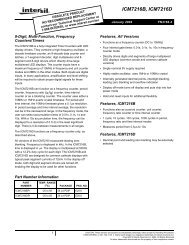
LM710 Voltage Comparator
LM710 Voltage Comparator
LM710 Voltage Comparator

You also want an ePaper? Increase the reach of your titles
YUMPU automatically turns print PDFs into web optimized ePapers that Google loves.
<strong>LM710</strong><br />
<strong>Voltage</strong> <strong>Comparator</strong><br />
General Description<br />
The <strong>LM710</strong> series are high-speed voltage comparators intended<br />
for use as an accurate, low-level digital level sensor<br />
or as a replacement for operational amplifiers in comparator<br />
applications where speed is of prime importance. The circuit<br />
has a differential input and a single-ended output, with saturated<br />
output levels compatible with practically all types of integrated<br />
logic.<br />
The device is built on a single silicon chip which insures low<br />
offset and thermal drift. The use of a minimum number of<br />
stages along with minority-carrier lifetime control (gold doping)<br />
makes the circuit much faster than operational amplifi-<br />
Schematic and Connection Diagrams<br />
DS010410-1<br />
ers in saturating comparator applications. In fact, the low<br />
stray and wiring capacitances that can be realized with<br />
monolithic construction make the device difficult to duplicate<br />
with discrete components operating at equivalent power levels.<br />
The <strong>LM710</strong> series are useful as pulse height discriminators,<br />
voltage comparators in high-speed A/D converters or go,<br />
no-go detectors in automatic test equipment. They also have<br />
applications in digital systems as an adjustable-threshold<br />
line receiver or an interface between logic types. In addition,<br />
the low cost of the units suggests them for applications replacing<br />
relatively simple discrete component circuitry.<br />
Ceramic Flatpak Package<br />
February 1995<br />
DS010410-9<br />
* Also available per JM38510/10301<br />
Order Number <strong>LM710</strong>AMW/883*<br />
See NS Package Number W10A<br />
© 1997 National Semiconductor Corporation DS010410 www.national.com 1<br />
PrintDate=1997/05/16 PrintTime=10:46:07 7730 ds010410 Rev. No. 1 Proof 1<br />
<strong>LM710</strong> <strong>Voltage</strong> <strong>Comparator</strong><br />
<strong>LM710</strong>
Schematic and Connection Diagrams (Continued)<br />
Pin 4 is connected to case.<br />
Metal Can Package<br />
* Also available per JM38510/10301<br />
DS010410-2<br />
Top View<br />
Order Number <strong>LM710</strong>AMH/883*, <strong>LM710</strong>H,<br />
<strong>LM710</strong>H/883 or <strong>LM710</strong>CH<br />
See NS Package Number H08C<br />
www.national.com 2<br />
Dual-In-Line Package<br />
DS010410-3<br />
Top View<br />
Order Number<br />
<strong>LM710</strong>AMJ/883* or <strong>LM710</strong>CN<br />
See NS Package Number N14A or J14A<br />
PrintDate=1997/05/16 PrintTime=10:46:07 7730 ds010410 Rev. No. 1 Proof 2
Absolute Maximum Ratings (Note *NO<br />
TARGET FOR FNXref NS0053*)<br />
If Military/Aerospace specified devices are required,<br />
please contact the National Semiconductor Sales Office/<br />
Distributors for availability and specifications.<br />
Positive Supply <strong>Voltage</strong> +14V<br />
Negative Supply <strong>Voltage</strong> −7V<br />
Peak Output Current 10 mA<br />
Output Short Circuit Duration 10 seconds<br />
Differential Input <strong>Voltage</strong> ±5V<br />
Input <strong>Voltage</strong> ±7V<br />
Electrical Characteristics (Note 3)<br />
Power Dissipation<br />
TO-99 (Note 1) 700 mW<br />
Plastic Dual-In-Line Package<br />
(Note 2) 950 mW<br />
Operating Temperature Range<br />
<strong>LM710</strong> −55˚C to +125˚C<br />
<strong>LM710</strong>C 0˚C to +70˚C<br />
Storage Temperature Range −65˚C to +150˚C<br />
Lead Temperature<br />
(Soldering, 10 sec.) 260˚C<br />
Parameter Conditions <strong>LM710</strong> <strong>LM710</strong>C Units<br />
Min Typ Max Min Typ Max<br />
Input Offset <strong>Voltage</strong> RS ≤ 200Ω, VCM = 0V, TA = 25˚C 0.6 2.0 1.6 5.0 mV<br />
Input Offset Current VOUT = 1.4V, TA = 25˚C 0.75 3.0 1.8 5.0 µA<br />
Input Bias Current TA = 25˚C 13 20 16 25 µA<br />
<strong>Voltage</strong> Gain TA = 25˚C 1250 1700 1000 1500<br />
Output Resistance TA = 25˚C 200 200 Ω<br />
Output Sink Current VOUT = 0, TA = 25˚C<br />
ΔVIN ≥ 5 mV 2.0 2.5 mA<br />
ΔVIN ≥ 10 mV 1.6 2.5 mA<br />
Response Time TA = 25˚C (Note 4) 40 40 ns<br />
Input Offset <strong>Voltage</strong> RS ≤ 200Ω, VCM = 0V 3.0 6.5 mV<br />
Average Temperature Coefficient TMIN ≤ TA ≤ TMAX 3.0 10 5.0 20 µV/˚C<br />
of Input Offset <strong>Voltage</strong> RS ≤ 50Ω<br />
Input Offset Current TA = TA MAX 0.25 3.0 7.5 µA<br />
TA = TA MIN 1.8 7.0 7.5 µA<br />
Average Temperature Coefficient 25˚C ≤ TA ≤ TMAX 5.0 25 15 50 nA/˚C<br />
of Input Offset Current TMIN ≤ TA ≤ 25˚C 15 75 24 100 nA/˚C<br />
Input Bias Current TA = TMIN 27 45 25 40 µA<br />
Input <strong>Voltage</strong> Range V− = −7V ±5.0 ±5.0 V<br />
Common-Mode Rejection Ratio RS ≤ 200Ω 80 100 70 98 dB<br />
Differential Input <strong>Voltage</strong> Range ±5.0 ±5.0 V<br />
<strong>Voltage</strong> Gain 1000 800 V/V<br />
Positive Output Level −5 mA ≤ IOUT ≤ 0<br />
VIN ≥ 5 mV 2.5 3.2 4.0 V<br />
VIN ≥ 10 mV 2.5 3.2 4.0 V<br />
Negative Output Level VIN ≥ 5 mV −1.0 −0.5 0 V<br />
VIN ≥ 10 mV −1.0 −0.5 0 V<br />
Output Sink Current VIN ≥ 5 mV, VOUT = 0<br />
TA = 125˚C 0.5 1.7 mA<br />
TA = −55˚C 1.0 2.3 mA<br />
VIN ≥ 10 mV, VOUT = 0<br />
0˚C ≤ TA ≤ +70˚C<br />
0.5 mA<br />
Positive Supply Current VIN ≥ 5 mV 5.2 9.0 mA<br />
VIN ≥ 10 mV 5.2 9.0 mA<br />
Negative Supply Current VIN ≥ 5 mV 4.6 7.0 mA<br />
VIN ≥ 10 mV 4.6 7.0 mA<br />
3 www.national.com<br />
PrintDate=1997/05/16 PrintTime=10:46:10 7730 ds010410 Rev. No. 1 Proof 3
Electrical Characteristics (Note 3) (Continued)<br />
Parameter Conditions <strong>LM710</strong> <strong>LM710</strong>C Units<br />
Min Typ Max Min Typ Max<br />
Power Consumption IOUT = 0<br />
VIN ≥ 5 mV 90 150 mW<br />
VIN ≥ 10 mV 150 mW<br />
Note 1: Rating applies for ambient temperatures of 25˚C; derate linearly at 5.6 mW/˚C for ambient temperatures above 25˚C.<br />
Note 2: Derate linearly at 9.5 mW/˚C for ambient temperatures above 25˚C.<br />
Note 3: These specifications appy for V + = 12V, V − = −6V, −55˚C ≤ TA ≤ +125˚C for <strong>LM710</strong> and 0˚C ≤ TA ≤ +70˚C for <strong>LM710</strong>C unless otherwise specified: The input<br />
offset voltage and input offset current (see definitions) are specified for a logic threshold voltage of 1.8V at −55˚C, 1.4V at 25˚C, and 1V at 125˚C for <strong>LM710</strong> and 1.5V<br />
at 0˚C, 1.4V at 25˚C, and 1.2V at 70˚C for <strong>LM710</strong>C.<br />
Note 4: The response time specified (see definitions) is for a 100 mV input step with 5 mV overdrive (<strong>LM710</strong>) or a 10 mV overdrive (<strong>LM710</strong>C).<br />
Typical Applications<br />
Schmitt Trigger<br />
Pulse Width Modulator<br />
DS010410-4<br />
DS010410-6<br />
www.national.com 4<br />
Line Receive with Increased<br />
Output Sink Current<br />
DS010410-5<br />
Level Detector with Lamp Driver<br />
PrintDate=1997/05/16 PrintTime=10:46:11 7730 ds010410 Rev. No. 1 Proof 4<br />
DS010410-7
Typical Performance Characteristics<br />
Transfer Function<br />
Input Bias Current<br />
Response Time for<br />
Various Input Overdrives<br />
DS010410-10<br />
DS010410-13<br />
DS010410-16<br />
<strong>Voltage</strong> Gain<br />
Input Offset Current<br />
Response Time for<br />
Various Input Overdrives<br />
DS010410-11<br />
DS010410-14<br />
DS010410-17<br />
<strong>Voltage</strong> Gain<br />
Supply Current<br />
Common Mode Pulse<br />
Response<br />
DS010410-12<br />
DS010410-15<br />
DS010410-18<br />
5 www.national.com<br />
PrintDate=1997/05/16 PrintTime=10:46:12 7730 ds010410 Rev. No. 1 Proof 5
Typical Performance Characteristics (Continued)<br />
Output <strong>Voltage</strong> Level<br />
DS010410-19<br />
Output Sink Current<br />
www.national.com 6<br />
DS010410-20<br />
Maximum Power Dissipation<br />
DS010410-21<br />
PrintDate=1997/05/16 PrintTime=10:46:12 7730 ds010410 Rev. No. 1 Proof 6<br />
Book<br />
Extract<br />
End
THIS PAGE IS IGNORED IN THE DATABOOK<br />
7<br />
PrintDate=1997/05/16 PrintTime=10:46:12 7730 ds010410 Rev. No. 1 Proof 7
Physical Dimensions inches (millimeters)<br />
Metal Can Package<br />
Order Number <strong>LM710</strong>AMH/883, <strong>LM710</strong>H, <strong>LM710</strong>H/883 or <strong>LM710</strong>CH<br />
NS Package Number H08C<br />
Ceramic Dual-In-Line Package<br />
Order Number <strong>LM710</strong>AMJ/883<br />
NS Package Number J14A<br />
www.national.com 8<br />
PrintDate=1997/05/16 PrintTime=10:46:13 7730 ds010410 Rev. No. 1 Proof 8
Physical Dimensions inches (millimeters) (Continued)<br />
Molded Dual-In-Line Package (N)<br />
Order Number <strong>LM710</strong>CN<br />
NS Package Number N14A<br />
Ceramic Flatpak<br />
Order Number <strong>LM710</strong>AMW/883<br />
NS Package Number W10A<br />
9 www.national.com<br />
PrintDate=1997/05/16 PrintTime=10:46:13 7730 ds010410 Rev. No. 1 Proof 9<br />
9
<strong>LM710</strong> <strong>Voltage</strong> <strong>Comparator</strong><br />
LIFE SUPPORT POLICY<br />
NATIONAL’S PRODUCTS ARE NOT AUTHORIZED FOR USE AS CRITICAL COMPONENTS IN LIFE SUPPORT DE-<br />
VICES OR SYSTEMS WITHOUT THE EXPRESS WRITTEN APPROVAL OF THE PRESIDENT OF NATIONAL SEMI-<br />
CONDUCTOR CORPORATION. As used herein:<br />
1. Life support devices or systems are devices or systems<br />
which, (a) are intended for surgical implant into<br />
the body, or (b) support or sustain life, and whose failure<br />
to perform when properly used in accordance<br />
with instructions for use provided in the labeling, can<br />
be reasonably expected to result in a significant injury<br />
to the user.<br />
National Semiconductor<br />
Corporation<br />
1111 West Bardin Road<br />
Arlington, TX 76017<br />
Tel: 1(800) 272-9959<br />
Fax: 1(800) 737-7018<br />
www.national.com<br />
National Semiconductor<br />
Europe<br />
Fax: (+49) 0-180-530 85 86<br />
Email: cnjwge@tevm2.nsc.com<br />
Deutsch Tel: (+49) 0-180-530 85 85<br />
English Tel: (+49) 0-180-532 78 32<br />
Français Tel: (+49) 0-180-532 93 58<br />
Italiano Tel: (+49) 0-180-534 16 80<br />
2. A critical component in any component of a life support<br />
device or system whose failure to perform can be reasonably<br />
expected to cause the failure of the life support<br />
device or system, or to affect its safety or effectiveness.<br />
National Semiconductor<br />
Hong Kong Ltd.<br />
13th Floor, Straight Block,<br />
Ocean Centre, 5 Canton Rd.<br />
Tsimshatsui, Kowloon<br />
Hong Kong<br />
Tel: (852) 2737-1600<br />
Fax: (852) 2736-9960<br />
National Semiconductor<br />
Japan Ltd.<br />
Tel: 81-043-299-2308<br />
Fax: 81-043-299-2408<br />
National does not assume any responsibility for use of any circuitry described, no circuit patent licenses are implied and National reserves the right at any time without notice to change said circuitry and specifications.<br />
PrintDate=1997/05/16 PrintTime=10:46:13 7730 ds010410 Rev. No. 1 Proof 10