Derwent World Patents Index (DWPI) - EPI ... - Thomson Reuters
Derwent World Patents Index (DWPI) - EPI ... - Thomson Reuters
Derwent World Patents Index (DWPI) - EPI ... - Thomson Reuters

You also want an ePaper? Increase the reach of your titles
YUMPU automatically turns print PDFs into web optimized ePapers that Google loves.
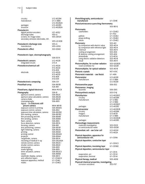
1112 Subject <strong>Index</strong><br />
circuitry U12-A02B4<br />
manufacture U11-C18B4<br />
U12-A02B2A<br />
packages U12-A02B3<br />
structure U12-A02B2A<br />
Photoelectric<br />
digital position encoders U21-A03J1<br />
discharge tubes V05-G<br />
screens, for image tubes V05-D05A1<br />
secondary emission electrodes, mfr.<br />
V05-L01A5B<br />
Photoelectric discharge tube V05-G<br />
manufacture V05-L05G<br />
Photoelectric effect S03-E06D<br />
Photoelectric layer, electrophotography<br />
S06-E01X<br />
Photoelectric sensors U12-A02B<br />
integrated circuits U13-A<br />
Photoelectrochemical cell U12-A02A<br />
X15-A02D<br />
X16-A04<br />
electrode U12-A02A<br />
X15-A02D<br />
X16-A04<br />
X16-E09<br />
Photoelectronic composing S06-C01<br />
Photoflash array S06-B03B<br />
X26-B01<br />
Photoframe, digital/electronic W04-P01C8<br />
Photography S06-B<br />
aperture control, camera S06-B02C<br />
aperture value calculation, camera S06-B02B<br />
camera shake S06-B02E<br />
cinematography S06-B05<br />
digital see Electronic still<br />
picture camera W04-M01B1<br />
exposure control in printing S06-B04A5<br />
exposure control, camera S06-B02<br />
exposure time calculation, camera S06-B02B2<br />
film marking, camera S06-B01B2<br />
film processing and mfr. S06-B04B<br />
film winding, camera S06-B08A<br />
flash, camera S06-B03<br />
focus detection, camera S06-B01A<br />
focusing, camera S06-B01<br />
lens positioning, camera S06-B01B1<br />
light metering, camera S06-B02A<br />
printing S06-B04A<br />
printing control S06-B04A5<br />
projector S06-B06A<br />
rangefinder, camera S06-B01A<br />
recording of medical X-ray S05-D02A5A<br />
remote control, camera S06-B02C1<br />
shutter control, camera S06-B02C<br />
stereoscopic S06-B09<br />
studio lighting S06-B09<br />
timer actuation, camera S06-B02C5<br />
viewer S06-B06B<br />
viewfinder display, camera S06-B01C<br />
anti-reflection layers U11-C04A1H<br />
exposure apparatus, method U11-C04E1<br />
masks U11-C04E2<br />
Photolithography, semiconductor<br />
manufacture U11-C04E<br />
Photoluminescence quenching thermometry<br />
S03-B01G<br />
Photomasks<br />
caseholders U11-C04E2<br />
U11-F02<br />
pellicle U11-C04E2<br />
phase shifting U11-C04E2<br />
reticle U11-C04E2<br />
Photometry S03-A01<br />
by comparison with electric value S03-A01A<br />
by comparison with reference light S03-A01A<br />
chemical S03-A01X<br />
cooling arrangement S03-A04<br />
IR detector cooling arrangement S03-A04<br />
photodiode U13-A01A<br />
using electric radiation detectors S03-A01B<br />
visual S03-A01X<br />
Photomultiplier, for nuclear radiation S03-G02B2E<br />
novel scintillator for S03-G02B1<br />
Photomultiplier, for optical radiation S03-A01B<br />
Photonic crystals V07-K10C<br />
Photoresist materials see Resist U11-A06<br />
Photoresistor U12-A02B1<br />
manufacture U11-C18B4<br />
U12-A02B1<br />
Photosensitive paper S06-E02<br />
Photosensor, imaging<br />
facsimile S06-D05<br />
Photosynthesis analysis S03-E14J<br />
Photothyristor U12-A02B2C<br />
circuitry U12-A02B4<br />
manufacture U11-C18B2<br />
U11-C18B4<br />
U12-A02B2C<br />
packages U12-A02B3<br />
Phototransistor U12-A02B2B<br />
circuitry U12-A02B4<br />
imagers U13-A01B<br />
manufacture U11-C18B4<br />
U12-A02B2B<br />
packages U12-A02B3<br />
Photovoltage measurements<br />
materials investigation S03-E02X<br />
on semiconductor wafer S03-G02B1<br />
Photovoltaic cell - see Solar cell U12-A02A1<br />
X15-A02A<br />
Physical deposition, apparatus for<br />
semiconductor mfr. U11-C09A<br />
Physical deposition, conductive layer<br />
U11-C05C2<br />
Physical deposition, insulating layer U11-C05B2<br />
Physical deposition, semiconductor layer<br />
U11-C01A<br />
evaporation, arc U11-C01A1<br />
evaporation, thermal U11-C01A1<br />
Physical therapy, medical S05-A05E<br />
Physical/chemical properties, investigating<br />
corrosion resistance S03-F07