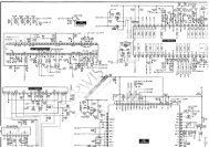
service manual sacd/dvd receiver - Diagramas Gratis - Diagramas ...
service manual sacd/dvd receiver - Diagramas Gratis - Diagramas ...
service manual sacd/dvd receiver - Diagramas Gratis - Diagramas ...

Create successful ePaper yourself
Turn your PDF publications into a flip-book with our unique Google optimized e-Paper software.
Pin No. Pin Name I/O Description<br />
43 DIP-RST O Reset signal output to the power amplifier “L”: reset<br />
44 DIP-OCP I Protect signal input from the power amplifier<br />
45 ST-POWER O System power on/off control signal output “H”: power on<br />
46 HP-MUTE O Headphone muting on/off control signal output “L”: muting on<br />
47 AU-MUTE O Audio line muting on/off control signal output “L”: muting on<br />
48 AV-SEL2 O Audio/video selection signal output<br />
49 PROG SW I SCAN SELECT switch input terminal “L”: SELECTABLE, “H”: INTERLACE<br />
50 TU-ON O Tuner power on/off control signal output “H”: power on<br />
51 TUNED I Tuning detection signal input from the tuner unit “L”: tuned<br />
52 TUN-DI I Serial data input from the tuner unit<br />
53 TUN-CE O Chip enable signal output to the tuner unit<br />
54 TUN-DO O Serial data output to the tuner unit<br />
55 TUN-CLK O Serial data transfer clock signal output to the tuner unit<br />
56 FL-MUTE O Reset signal output to the fluorescent indicator tube driver “L”: reset<br />
HCD-S550/S880<br />
57 FL-CLK O Serial data transfer clock signal output to the LED driver and fluorescent indicator tube driver<br />
58 BVDD — Power supply terminal (+5V) (for bus interface)<br />
59 BVSS — Ground terminal (for bus interface)<br />
60 FL-DATA O Serial data output to the LED driver and fluorescent indicator tube driver<br />
61 FL-CS O Chip select signal output to the fluorescent indicator tube driver “L” active<br />
62 LED-CS O Standby signal output to the LED driver “L”: standby<br />
63 LED-CLR O Reset signal output to the LED driver “L”: reset<br />
64 HPSW I<br />
Connection detection signal input of the headphone jack<br />
“L”: no connected, “H”: headphone connected<br />
65 DFIL RST2 O Reset signal output to the digital audio processor “L”: reset<br />
66 SP RELAY O Relay drive signal output terminal for the speaker protect Not used<br />
67 PARA-DO2 I Serial data input from the mechanism deck controller<br />
68 PARA-RST O Reset signal output to the mechanism deck controller “L”: reset<br />
69 PARA-LT1 O Serial data latch pulse signal output to the mechanism deck controller<br />
70 PARA-LT2 O Serial data latch pulse signal output terminal Not used<br />
71 PARA-CLK O Serial data transfer clock signal output to the mechanism deck controller<br />
72 PARA-DATA O Serial data output to the mechanism deck controller<br />
73 PARA-DO1 I Serial data input terminal Not used<br />
74 AVDD — Power supply terminal (+5V) (analog system)<br />
75 AVSS — Ground terminal (analog system)<br />
76 AVREF I Reference voltage (+5V) input terminal (analog system)<br />
77 NO USE — Not used<br />
78 OPT-SEN2 I Disc insert detection signal input from the photo sensor<br />
79 OPT-SEN I Chucking detection signal input from the photo sensor<br />
80 AREA1 I Destination setting terminal<br />
81 SEN2 I Disc in/out switch input terminal “L”: when a disc is inserted<br />
82 to 84 KEY0 to KEY2 I Key input terminal (A/D input)<br />
85 EN-A I Jog dial pulse input from the rotary encoder (A phase input)<br />
86 EN-B I Jog dial pulse input from the rotary encoder (B phase input)<br />
87 MODEL I Model setting terminal<br />
88 RDS-DATA I RDS serial data input from the RDS decoder (AEP, UK and Russian models only)<br />
89 DVD-POWER O DVD power on/off control signal output “H”: power on<br />
90 STOP I System stop signal input<br />
91 POWER-SW I System power on/off control signal input “H”: power on<br />
99