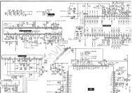
service manual sacd/dvd receiver - Diagramas Gratis - Diagramas ...
service manual sacd/dvd receiver - Diagramas Gratis - Diagramas ...
service manual sacd/dvd receiver - Diagramas Gratis - Diagramas ...

Create successful ePaper yourself
Turn your PDF publications into a flip-book with our unique Google optimized e-Paper software.
HCD-S550/S880<br />
• DVD BOARD IC901 µPD70F3033BYGF-M10-3BA (SYSTEM CONTROLLER)<br />
98<br />
Pin No. Pin Name I/O Description<br />
1 DAMP-DATA O Serial data output to the stream processors<br />
2 DAMP-CLK O Serial data transfer clock signal output to the stream processors<br />
3 I2C-DATA I/O Communication data bus with the DVD system processor and mechanism controller<br />
4 CQ-RST O Reset signal output to the DVD system processor “L”: reset<br />
5 I2C-CLK I/O<br />
Communication data reading clock signal input or transfer clock signal output with the DVD<br />
system processor and mechanism controller<br />
6 DSP-DO I Write data input from the digital audio signal processor<br />
7 DIG-DI O<br />
Read data output to the digital audio interface IC, digital audio signal processor and D/A<br />
converter<br />
8 DIG-CLK O<br />
Clock signal output to the digital audio interface IC, digital audio signal processor and D/A<br />
converter<br />
9 EVDD — Power supply terminal (+5V)<br />
10 EVSS — Ground terminal<br />
11 P-PWM O PWM voltage control signal output<br />
12 DSP-RST O Reset signal output to the digital audio signal processor “L”: reset<br />
13 DSP-PM O PLL reset signal output to the digital audio signal processor “L”: reset<br />
14 DSP-CS O Chip select signal output to the digital audio signal processor<br />
15 DSP-HACN I Acknowledge signal input from to the digital audio signal processor<br />
16 DSP-BST O Boot trap signal output to the digital audio signal processor<br />
17 DSP-GP9 I Decode signal input from to the digital audio signal processor<br />
18 DIR-ZERO I Audio serial data input from the digital audio interface IC<br />
19 DIR-ERR I PLL lock error and data error flag input from the digital audio interface IC<br />
20 DIR-CE O Chip enable signal output to the digital audio interface IC<br />
21 VPP — Power supply terminal (for programming) Not used<br />
22 DIR-XST I Source clock switching monitor input from the digital audio interface IC<br />
23 DIR-AD O Not used<br />
24 DIR-XMODE I System reset signal input from the digital audio interface IC “L”: reset<br />
25 DIRDO I Write data input from the digital audio interface IC<br />
26 DAMP-RST O Reset signal output to the stream processors “L”: reset<br />
27 DAMP-MUTEG O Muting on/off control signal output to the stream processors “H”: muting on<br />
28 DAMP-MUTEN O Muting on/off control signal output to the stream processors “H”: muting on<br />
29 CS1 O Chip select signal output to the stream processor (for front L-ch and R-ch)<br />
30 CS2 O Chip select signal output to the stream processor (for center and woofer)<br />
31 CS3 O Chip select signal output to the stream processor (for rear L-ch and R-ch)<br />
32 DAC-CS O Chip select signal output to the D/A converter<br />
33 AD-RST O Reset signal output to the A/D converter and D/A converter “L”: reset<br />
34 RESET I<br />
System reset signal input “L”: reset<br />
For several hundreds msec. after the power supply rises, “L” is input, then it changes to “H”<br />
35 XT1 I Sub system clock input terminal Not used<br />
36 XT2 O Sub system clock output terminal Not used<br />
37 REG0 — Not used<br />
38 X2 O Main system clock output terminal (20 MHz)<br />
39 X1 I Main system clock input terminal (20 MHz)<br />
40 VSS — Ground terminal<br />
41 VDD — Power supply terminal (+5V)<br />
42 CLKOUT O Clock signal output terminal Not used