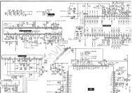
service manual sacd/dvd receiver - Diagramas Gratis - Diagramas ...
service manual sacd/dvd receiver - Diagramas Gratis - Diagramas ...
service manual sacd/dvd receiver - Diagramas Gratis - Diagramas ...

You also want an ePaper? Increase the reach of your titles
YUMPU automatically turns print PDFs into web optimized ePapers that Google loves.
HCD-S550/S880<br />
92<br />
Pin No. Pin Name I/O Description<br />
53 XSRQ I<br />
DVD mode: Serial data request signal input from the DVD system processor<br />
SACD mode: Serial data request signal input from the DSD decoder<br />
54 HINT O Not used<br />
55 XS16 O Not used<br />
56 HA1 I Not used<br />
57 XPDI I/O Not used<br />
58 VDDS — Power supply terminal (+5V) (digital system)<br />
59, 60 HA0, HA2 I Not used<br />
61 VSS — Ground terminal (digital system)<br />
62, 63 HCS0, HCS1 I Not used<br />
64 VDD — Power supply terminal (+3.3V) (digital system)<br />
65 DASP I/O Not used<br />
66 to 69 MDB0 to MDB3 I/O Two-way data bus with the D-RAM<br />
70 VSS — Ground terminal (digital system)<br />
71 MDB4 I/O Two-way data bus with the D-RAM<br />
72 VDD5V — Power supply terminal (+5V)<br />
73 to 75 MDB5 to MDB7 I/O Two-way data bus with the D-RAM<br />
76 XMWR O Write enable signal output to the D-RAM<br />
77 VDD — Power supply terminal (+3.3V) (digital system)<br />
78 XRAS O Row address strobe signal output to the D-RAM<br />
79, 80 MA0, MA1 O Address signal output to the D-RAM<br />
81 VSS — Ground terminal (digital system)<br />
82 to 87 MA2 to MA7 O Address signal output to the D-RAM<br />
88 VDD — Power supply terminal (+3.3V) (digital system)<br />
89 MA8 O Address signal output to the D-RAM<br />
90 VSS — Ground terminal (digital system)<br />
91 MA9 O Address signal output to the D-RAM<br />
92 MNT1 O EEPROM ready signal output to the mechanism controller<br />
93 MNT2 O Operation clock signal output for PSP physical disc mark detection to DSD decoder<br />
94 XMOE O Output enable signal output to the D-RAM<br />
95 XCAS O Column address strobe signal output to the D-RAM<br />
96, 97 MDB8, MDB9 I/O Two-way data bus with the D-RAM<br />
98 VSS — Ground terminal (digital system)<br />
99 MDBA I/O Two-way data bus with the D-RAM<br />
100 VDD — Power supply terminal (+3.3V) (digital system)<br />
101, 102 MDBB, MDBC I/O Two-way data bus with the D-RAM<br />
103 VDD5V — Power supply terminal (+5V)<br />
104 to 106 MDBD to MDBF I/O Two-way data bus with the D-RAM<br />
107 GFS O Guard frame sync signal output to the mechanism controller<br />
108 VSS — Ground terminal (digital system)<br />
109 APEO O Absolute phase error signal output<br />
110 VDD — Power supply terminal (+3.3V) (digital system)<br />
111 DASYO O RF binary signal output<br />
112 GNDA5 — Ground terminal (analog system)<br />
113, 114 ASF1, AFS2 — Filter connected terminal for selection the constant asymmetry compensation<br />
115 DASYI I Analog signal input after integrated from the RF binary signal