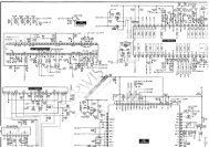
service manual sacd/dvd receiver - Diagramas Gratis - Diagramas ...
service manual sacd/dvd receiver - Diagramas Gratis - Diagramas ...
service manual sacd/dvd receiver - Diagramas Gratis - Diagramas ...

Create successful ePaper yourself
Turn your PDF publications into a flip-book with our unique Google optimized e-Paper software.
HCD-S550/S880<br />
• DVD BOARD IC607 CXD9617R (DIGITAL AUDIO SIGNAL PROCESSOR)<br />
88<br />
Pin No. Pin Name I/O Description<br />
1 VSS — Ground terminal<br />
2 XRST I Reset signal input from the system controller “L”: reset<br />
3 EXTIN I Master clock signal input terminal Not used<br />
4 FS2 I Sampling frequency selection signal input terminal Not used<br />
5 VDDI — Power supply terminal (+2.6V)<br />
6 FS1 I Sampling frequency selection signal input terminal Not used<br />
7 PLOCK O Internal PLL lock signal output terminal Not used<br />
8 VSS — Ground terminal<br />
9 MCLK1 I System clock signal input terminal (13.5 MHz)<br />
10 VDDI — Power supply terminal (+2.6V)<br />
11 VSS — Ground terminal<br />
12 MCLK2 O System clock signal output terminal (13.5 MHz)<br />
13 MS I Master/slave selection signal input terminal “L”: slave, “H”: master (fixed at “L” in this set)<br />
14 SCKOUT O Internal system clock signal output to the D/A converter and stream processor<br />
15 LRCKI1 I L/R sampling clock signal (44.1 kHz) input from the digital audio processor<br />
16 VDDE — Power supply terminal (+3.3V)<br />
17 BCKI1 I Bit clock signal (2.8224 MHz) input from the digital audio processor<br />
18 SDI1 I Front L-ch and R-ch audio serial data input from the digital audio processor<br />
19 LRCKO O L/R sampling clock signal (44.1 kHz) output to the D/A converter and stream processor<br />
20 BCKO O Bit clock signal (2.8224 MHz) output to the D/A converter and stream processor<br />
21 VSS — Ground terminal<br />
22 KFSIO I Audio clock signal (11.2896 MHz) input from the digital audio processor<br />
23 SDO1 O Front L-ch and R-ch audio serial data output to the stream processor<br />
24 SDO2 O Center and woofer audio serial data output to the stream processor<br />
25 SDO3 O Rear L-ch and R-ch audio serial data output to the stream processor<br />
26 SDO4 O Audio serial data output to the D/A converter<br />
27 SPDIF O S/PDIF signal output terminal Not used<br />
28 LRCKI2 I L/R sampling clock signal (44.1 kHz) input from the A/D converter<br />
29 BCKI2 I Bit clock signal (2.8224 MHz) input from the A/D converter<br />
30 SDI2 I Center and woofer audio serial data input from the digital audio processor<br />
31 VSS — Ground terminal<br />
32 HACN O Acknowledge signal output to the system controller<br />
33 HDIN I Write data input from the system controller<br />
34 HCLK I Clock signal input from the system controller<br />
35 HDOUT O Read data output to the system controller<br />
36 HCS I Chip select signal input from the system controller<br />
37 SDCLK O Clock signal output terminal Not used<br />
38 CLKEN O Clock enable signal output terminal Not used<br />
39 RAS O Row address strobe signal output terminal Not used<br />
40 VDDI — Power supply terminal (+2.6V)<br />
41 VSS — Ground terminal<br />
42 CAS O Column address strobe signal output terminal Not used<br />
43 DQM O Output terminal of data input/output mask Not used<br />
44 CS0 O Chip select signal output to the S-RAM<br />
45 WE0 O Write enable signal output to the S-RAM