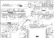
service manual sacd/dvd receiver - Diagramas Gratis - Diagramas ...
service manual sacd/dvd receiver - Diagramas Gratis - Diagramas ...
service manual sacd/dvd receiver - Diagramas Gratis - Diagramas ...

Create successful ePaper yourself
Turn your PDF publications into a flip-book with our unique Google optimized e-Paper software.
Pin No. Pin Name I/O Description<br />
47 AVDD0 — Power supply terminal (+3.3V) (analog system)<br />
48 ASYO O EFM full-swing output terminal<br />
49 ASYI I Asymmetry comparator voltage input terminal<br />
50 RFAC I EFM signal input from the DVD/CD RF amplifier<br />
51 AVSS1 — Ground terminal (analog system)<br />
52 CLTV I Internal VCO control voltage input terminal<br />
53 FILO O Filter output for master PLL<br />
54 FILI I Filter input for master PLL<br />
55 PCO O Charge pump output for master PLL<br />
56 AVDD1 — Power supply terminal (+3.3V) (analog system)<br />
57 BIAS I Asymmetry circuit constant current input terminal<br />
58 VCTL I VCO control voltage input terminal for the wideband EFM PLL Not used<br />
59 V16M O VCO oscillation output terminal for the wideband EFM PLL Not used<br />
60 VPCO O Charge pump output terminal for the wideband EFM PLL Not used<br />
61 DVDD2 — Power supply terminal (+3.3V) (digital system)<br />
HCD-S550/S880<br />
62 ASYE I Asymmetry circuit on/off control signal input terminal “L”: off, “H”: on Not used<br />
63 MD2 I<br />
Digital out on/off control signal input from the mechanism controller<br />
“L”: digital out off, “H”: digital out on<br />
64 DOUT O Digital audio signal output to the digital audio interface IC<br />
65 LRCK O L/R sampling clock signal (44.1 kHz) output to the DVD decoder<br />
66 PCMD O Serial data output to the DVD decoder<br />
67 BCK O Bit clock signal (2.8224 MHz) output to the DVD decoder<br />
68 EMPH O<br />
“L” is output when playback disc is emphasis off<br />
“H” is output when playback disc is emphasis on Not used<br />
69 XTSL I<br />
Input terminal for the system clock frequency setting<br />
“L”: 16.9344 MHz, “H”: 33.8688MHz Fixed at “H” in this set<br />
70 DVSS2 — Ground terminal (digital system)<br />
71 XTAI I System clock input terminal (33.8688 MHz)<br />
72 XTAO O System clock output terminal (33.8688 MHz) Not used<br />
73 SOUT O Serial data output terminal Not used<br />
74 SOCK O Serial data reading clock signal output terminal Not used<br />
75 XOLT O Serial data latch pulse signal output terminal Not used<br />
76 SQSO O Subcode Q data output to the mechanism controller<br />
77 SQCK I Subcode Q data reading clock signal input from the mechanism controller<br />
78 SCSY I Input terminal for resynchronism of guard subcode sync (S0+S1) Not used<br />
79 SBSO O Subcode serial data output to the DVD decoder<br />
80 EXCK I Subcode serial data reading clock signal input to the DVD decoder<br />
87