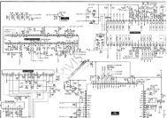
service manual sacd/dvd receiver - Diagramas Gratis - Diagramas ...
service manual sacd/dvd receiver - Diagramas Gratis - Diagramas ...
service manual sacd/dvd receiver - Diagramas Gratis - Diagramas ...

You also want an ePaper? Increase the reach of your titles
YUMPU automatically turns print PDFs into web optimized ePapers that Google loves.
Pin No. Pin Name I/O Description<br />
53 MUTE DSD O Muting on/off control signal output to the DSD decoder “H”: muting on<br />
54 SQCK O Subcode Q data reading clock signal output to the digital signal processor<br />
55 VSS — Ground terminal (digital system)<br />
56 TRAY IN I Disc tray in detection signal input terminal Not used<br />
57 TRAY OUT I Disc tray out detection signal input terminal Not used<br />
58 GFS DVD I Guard frame sync signal input from the DVD decoder<br />
59 MUTE CD O Muting on/off control signal output to the digital signal processor “H”: muting on<br />
60 MUTE 2D O Muting on/off control signal output to the motor/coil driver “H”: muting on<br />
61 SLED I Sled motor servo drive PWM signal input terminal<br />
62 FG I Spindle motor control signal input<br />
63 SP ON O Muting on/off control signal output to the motor/coil driver “H”: muting on<br />
64 JIT I Jitter signal input<br />
65 TE I Tracking error signal input from the DVD/CD RF amplifier<br />
66 PI I Pull in signal input from the DVD/CD RF amplifier<br />
67 FE I Focus error signal input from the DVD/CD RF amplifier<br />
68 AVSS — Ground terminal (for A/D converter)<br />
69 AVREF I Reference voltage input terminal (for A/D converter)<br />
70 AVDD — Power supply terminal (+3.3V) (for A/D converter)<br />
71 GFS CD I Guard frame sync signal input from the digital signal processor<br />
72 SCLK CD O SENSE serial data reading clock signal output to the digital signal processor<br />
73 TSD O Thermal shut down signal output to the motor/coil driver<br />
74 FOK CD I Focus OK signal input from the digital signal processor<br />
75 LOCK CD I GFS is sampled by 460 Hz “H” input when GFS is “H”<br />
76 LDSEL O Laser diode selection signal output<br />
77 SACD/DVD O SACD/DVD selection signal output “L”: DVD, “H”: SACD<br />
78 I2C SIO I/O Communication data bus with the DVD system processor and system controller<br />
79 I2C SCL I/O<br />
HCD-S550/S880<br />
Communication data reading clock signal input or transfer clock signal output with the DVD<br />
system processor and system controller<br />
80 RXD I Serial data input from the RS-232C (for check)<br />
81 TXD O Serial data output to the RS-232C (for check)<br />
82 SDCLK RF O Serial data transfer clock signal output to the DVD/CD RF amplifier<br />
83 SDATA RF I/O Two-way data bus with the DVD/CD RF amplifier<br />
84 XWR O Write strobe signal output to the DVD decoder<br />
85 XRD O Read strobe signal output to the DVD decoder<br />
86 (PWE) — Not used<br />
87 VDD — Power supply terminal (+3.3V) (digital system)<br />
88 VSS — Ground terminal (digital system)<br />
89 to 96 A0 to A7 O Address signal output to the DVD decoder<br />
97 DSAVE O Motor/coil driver power save control signal output terminal Not used<br />
98 XDRST O Reset signal output to the digital signal processor and DSD decoder “L”: reset<br />
99 EEP WP O Write protect signal output to the EEPROM<br />
100 EEP CLK O Clock signal output to the EEPROM<br />
85