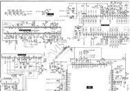
service manual sacd/dvd receiver - Diagramas Gratis - Diagramas ...
service manual sacd/dvd receiver - Diagramas Gratis - Diagramas ...
service manual sacd/dvd receiver - Diagramas Gratis - Diagramas ...

Create successful ePaper yourself
Turn your PDF publications into a flip-book with our unique Google optimized e-Paper software.
HCD-S550/S880<br />
7-40. IC PIN FUNCTION DESCRIPTION<br />
• DVD BOARD IC301 CXP973064-224R (MACHANISM CONTROLLER)<br />
84<br />
Pin No. Pin Name I/O Description<br />
1 EEP SO O Not used<br />
2 SDEN O Serial data enable signal output to DVD/CD RF amplifier<br />
3<br />
DOCTRL/<br />
ISBTEST<br />
O<br />
Digital out on/off control signal output to the digital signal processor<br />
“L”: digital out off, “H”: digital out on<br />
4 EEP WC O Not used<br />
5 EEP SI I/O Two-way data bus with the EEPROM<br />
6 EEP RDY I EEPROM ready signal input from the DVD decoder<br />
7 FCS JMP 1 O Focus jump 1 signal output to the motor/coil driver<br />
8 FCS JMP 2 O Focus jump 2 signal output to the motor/coil driver<br />
9 SENS CD I Internal status (SENSE) signal input from the digital signal processor<br />
10 LOAD+ O Loading motor drive signal (loading in direction) output terminal Not used<br />
11 LOAD– O Loading motor drive signal (loading out direction) output terminal Not used<br />
12 XCS DVD O Chip select signal output to the DVD decoder<br />
13 VSS — Ground terminal (digital system)<br />
14 to 21 D0 to D7 I/O Two-way data bus with the DVD decoder<br />
22 INIT0 DVD I Interrupt signal input from the DVD decoder<br />
23 INIT1 DVD I Interrupt signal input from the DVD decoder<br />
24 SCK DSD O Serial data transfer clock signal output to the DSD decoder<br />
25 XRST DVD O Reset signal output to the DVD decoder “L”: reset<br />
26 SCOR I Subcode sync (S0+S1) detection signal input from the digital signal processor<br />
27 LAT CD O Serial data latch pulse signal output to the digital signal processor<br />
28 LD ON O<br />
Laser diode on/off control signal output to the DVD/CD RF amplifier<br />
“L”: laser diode off, “H”: laser diode on<br />
29 MIRR I Mirror signal input from the digital signal processor<br />
30 COUT CD I Numbers of track counted signal input from the digital signal processor<br />
31 INLIM I Detection signal input from limit in switch The optical pick-up is inner position when “H”<br />
32 CS ZIVA O Chip select signal output to the DVD system processor<br />
33 SI ZIVA I Serial data input from the DVD system processor<br />
34 SO ZIVA O Serial data output to the DVD system processor<br />
35 SCK ZIVA O Serial data transfer clock signal output to the DVD system processor<br />
36 DRVIRQ O Interrupt request signal output to the DVD system processor<br />
37 DRVRDY O Ready signal output to the DVD system processor<br />
38 RST I System reset signal input from the DVD system processor “L”: reset<br />
39 VSS — Ground terminal (digital system)<br />
40 XTAL I System clock input terminal (20 MHz)<br />
41 EXTAL O System clock output terminal (20 MHz)<br />
42 VDD — Power supply terminal (+3.3V) (digital system)<br />
43, 44 SLED A, SLED B O Sled motor drive signal output<br />
45 JIT OFFSET O Output terminal for offset adjustment of APEO (