Spectrum E39

Create successful ePaper yourself
Turn your PDF publications into a flip-book with our unique Google optimized e-Paper software.
Electron micrsocopy/Materials science<br />
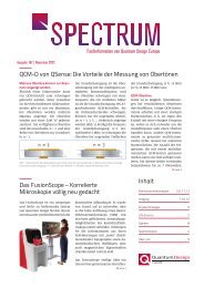
The FusionScope - correlated microscopy completely rethought<br />
New users will find correlative microscopy<br />
easy and accessible, while<br />
experienced users will be equipped<br />
with a powerful tool that<br />
contains the SEM and AFM functionality,<br />
they are familiar with.<br />
With Profile View – an 80-degree tilt<br />
of the combined sample stage and<br />
AFM scan head – you can position the<br />
AFM tip quickly and precisely, even on<br />
complex and challenging sample surfaces.<br />
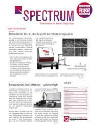
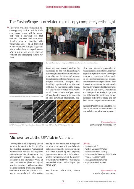
Our team from Quantum Design at MNE 2022 at the launch of the new FusionScope.<br />
Profile View with the FusionScope from a bone surface<br />
Focus on your research and let FusionScope<br />
do the rest. FusionScope’s<br />
software provides an intuitive and customizable<br />
user interface and integrates<br />
automation of most functions into<br />
helpful workflows. Intelligent data<br />
handling organizes all your SEM and<br />
AFM data for easy access in the future.<br />
Use the FusionScope for detailed Material<br />
Characterization of your samples<br />
and perform correlative analysis<br />
of their structural, mechanical, electrical,<br />
and magnetic properties on<br />
your exact region of interest. Carry out<br />
high-level Quality Control of component<br />
parts or perform Failure Analysis<br />
on electrical components or semiconductor<br />
devices as you benefit from<br />
FusionScope’s fast and intuitive workflow.<br />
Easily characterize Nanostructures<br />
such as nanowires, 2D-materials,<br />
and nanoparticles. FusionScope gives<br />
you full control to locate your area of<br />
interest, position your probe, and perform<br />
a wide range of measurements.<br />
Interested? Learn more about the specific<br />
details of the FusionScope on our<br />
new website: www.fusionscope.com<br />
(Left) Profile view of CPU chip and cantilever. (Middle) SEM image of CP chip (Right) AFM image of CPU chip<br />
Please contact us<br />
germany@qd-microscopy.com<br />
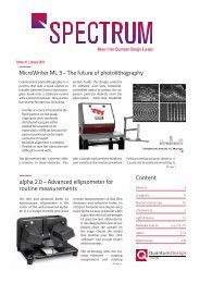
Microwriter at the UPVfab in Valencia<br />
To complete the lithography line of<br />
its microfabrication facility UPVfab,<br />
the Spanish University "Universitat<br />
Politècnica de València" has acquired<br />
a MicroWriter 3 Pro direct-write photolithography<br />
system. The microfabrication<br />
line includes 500 m2 of<br />
ISO-7 clean rooms (class 10 000) and<br />
positions equipped with automation<br />
tools for backend processing of semiconductor<br />
wafers. As part of a strategy<br />
to equip the microfabrication<br />
facility in the technical disciplines<br />
of photonics, electronics and chemical<br />
engineering, the new equipment<br />
has been funded by the Regional<br />
Government Generalitat Valenciana,<br />
within the framework of the project<br />
GVA/IDIFEDER/2021/046 "Multi-level<br />
Microfabrication Technologies (T-<br />
MFAB-MN)".<br />
For further information, please<br />
contact:<br />
UPVfab<br />
■ Dr. Gloria Micó<br />
■ Facility Manager, UPVfab<br />
Microfabrication Facility,<br />
■ Universitat Politècnica de València<br />
■ Phone: +34.963.879.760<br />
■ Mail: gloria.mico@upv.es<br />
■ https://www.fab.upv.es/<br />
Please contact us<br />
materials@qd-europe.com<br />
3 <strong>Spectrum</strong>, International edition 39| December 2022