Spectrum E39

Create successful ePaper yourself
Turn your PDF publications into a flip-book with our unique Google optimized e-Paper software.
Materials science<br />
MicroWriter – Our Direct-Writing Lithography System with<br />
Clever Features<br />
This basic principle is now extended<br />
by various options for the writing<br />
quality - irrespective of the resolution<br />
used. The feature "Automatic Pixel<br />
Smoothing" gives users the option<br />
to decide about the quality of the<br />
edges of the structures to be written.<br />
Fig. 3<br />
Fig. 1<br />
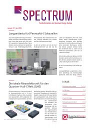
High resolution and fast writing -<br />
these are the typical requirements<br />
for a direct-writing photolithography<br />
system. However, high resolution<br />
compromises writing speed<br />
and vice versa. For this reason, the<br />
developers of our MicroWriter systems<br />
have put much thought into<br />
the question of how these two requirements<br />
can be reconciled as<br />
far as possible. Even the first generation<br />
of the MicroWriter allowed<br />
the user to select different resolutions<br />
for different objects. The highest<br />
resolution is selected only for<br />
those objects for which high resolution<br />
is really important, whereas<br />
a lower resolution is chosen for<br />
objects for which high resolution<br />
is not an absolute must, which comes<br />
with the benefit of a higher<br />
writing speed.<br />
Fig. 2<br />
The example in figure 1 shows the<br />
difference. The gap width of the coil<br />
is 2.5 µm and the resolution of writing<br />
was 1 µm. The roughness of the<br />
edges can typically be observed in<br />
the outstanding range of 30 nm. If<br />
this feature is not used, the writing<br />
speed increases dramatically, however,<br />
at the expense of edge quality.<br />
Fig. 4<br />
The second important feature is<br />
the so-called "Virtual Mask Aligner",<br />
which offers the possibility of placing<br />
the object to be written over the<br />
optical image of the sample surface.<br />
This is very helpful<br />
if structures<br />
to be written<br />
are to be aligned<br />
with structures<br />
that are already<br />
on the surface. A<br />
typical example<br />
are contact pads<br />
for e.g. graphene<br />
or 2D materials.<br />
Figure 2 shows<br />
how this looks<br />
in the software,<br />
while figure 3 is<br />
an actual result<br />
from one of our<br />
customers (courtesy<br />
of UGC-DAE Consortium for<br />
Scientific Research, Indore, India).<br />
The last feature is the "Wide Field<br />
Viewer". This feature allows you to<br />
quickly and easily generate a larger<br />
overview image of the sample surface.<br />
The system automatically circles<br />
the starting point, capturing one<br />
optical image at a time. Each further<br />
image will be stitched together<br />
to create an ever larger overview<br />
image. This feature can be used, e.g.,<br />
to find alignment markers or to<br />
look at already written structures<br />
for a first inspection.<br />
Please contact us<br />
materials@qd-europe.com<br />
14