Spectrum E39

Create successful ePaper yourself
Turn your PDF publications into a flip-book with our unique Google optimized e-Paper software.
News from Quantum Design Europe<br />
Edition 39 | December 2022<br />
We Keep Science Running – Merck Corporate Run in Darmstadt<br />
After a seemingly endless break of<br />
almost two years due to the pandemic,<br />
the Merck corporate run in<br />
Darmstadt took place again this<br />
year. To us, it was no question that<br />
we would definitely take on the<br />
challenge and participate in this<br />
event again. So we worked out an<br />
appropriate outfit to create a uniform<br />
look, and some of us may<br />
also have done some training in<br />
preparation of the run...<br />
A total of 4715 running enthusiasts<br />
turned up to participate. Everyone<br />
could choose their running distance<br />
between 3.33, 6.66 or 9.99 km, circling<br />
the Darmstadt "Messplatz" square.<br />
Despite the great heat, all of our 20<br />
runners, distributed over all starting<br />
groups, were lucky enough to reach<br />
the finish line. Indeed, it was a super<br />
hot day, with the heat coming from<br />
Page 2<br />
FusionScope<br />
Open a World of Easy-to-Use Correlative<br />
Microscopy by combining<br />
SEM with AFM in All New Ways<br />
FusionScope is an easy-to-use correlative<br />
microscopy platform designed<br />
from the ground up to provide<br />
the benefits of SEM imaging together<br />
with a wide range of AFM measurement<br />
techniques. Combine SEM<br />
information with three-dimensional<br />
topography, the characterization<br />
of nano-mechanical, conductive,<br />
and magnetic properties, and much<br />
more.<br />
FusionScope uses an innovative shared<br />
coordinate system to automatically<br />
align AFM and SEM operations<br />
for measurements and sample positioning.<br />
Within a single software interface,<br />
you can easily identify your<br />
area of interest, measure your sample,<br />
and combine your imaging data<br />
in real time.<br />
Page 3<br />
Content<br />
About us 2, 7, 12<br />
Cryogenics 9, 10<br />
Electron microscopy 2, 3<br />
Imaging 2, 6, 8<br />
Life Sciences 13<br />
Materials science 3, 7, 14, 16<br />
Optics 4, 6, 10<br />
Spectroscopy 11<br />
EUROPE
About us/Imaging<br />
We Keep Science Running – Merck Corporate Run in Darmstadt<br />
just everywhere, emanating from the<br />
asphalt and creeping up towards the<br />
brave runners. Of course, the organizer<br />
was prepared. All along the way,<br />
abundant drinks were provided and<br />
the local fire department even refreshed<br />
us with a cooling shower from<br />
above.<br />
Having passed the finish line, a warm<br />
welcome awaited us and we were treated<br />
to plenty of food and drink. The<br />
approaching thunderstorm did not<br />
keep us from having fun at the party.<br />
What a pity that eventually, we had<br />
to leave early due to lack of shelter<br />
against the rain.<br />
Overall, it was a successful event that<br />
strengthened the team spirit. We are<br />
happy to have been a part of it!<br />
Please contact us<br />
spectrum@qd-europe.com<br />
NewHigh Power X-Ray Sources for XRF and<br />
Imaging Applications<br />
The HPC high power tubes are designed<br />
to be used in XRF and imaging<br />
applications. As "targets", tungsten<br />
and molybdenum are available.<br />
10-75 kV range with constant power<br />
consumption up to 350 watts.<br />
The tube is air cooled and the<br />
"push/pull" configuration enables<br />
the warm air to be guided to the<br />
outside.<br />
For XRF applications, the cone<br />
is vacuum-sealed at the base.<br />
The HPC tube incorporates radiation<br />
shielding.<br />
Typical applications are, e.g.:<br />
■ Food inspection<br />
■ Thickness gauging<br />
■ Scrap metal recognition and<br />
sorting<br />
HPC High-power tube with power supply<br />
Please contact us<br />
imaging@qd-europe.com<br />
2
Electron micrsocopy/Materials science<br />
The FusionScope - correlated microscopy completely rethought<br />
New users will find correlative microscopy<br />
easy and accessible, while<br />
experienced users will be equipped<br />
with a powerful tool that<br />
contains the SEM and AFM functionality,<br />
they are familiar with.<br />
With Profile View – an 80-degree tilt<br />
of the combined sample stage and<br />
AFM scan head – you can position the<br />
AFM tip quickly and precisely, even on<br />
complex and challenging sample surfaces.<br />
Our team from Quantum Design at MNE 2022 at the launch of the new FusionScope.<br />
Profile View with the FusionScope from a bone surface<br />
Focus on your research and let FusionScope<br />
do the rest. FusionScope’s<br />
software provides an intuitive and customizable<br />
user interface and integrates<br />
automation of most functions into<br />
helpful workflows. Intelligent data<br />
handling organizes all your SEM and<br />
AFM data for easy access in the future.<br />
Use the FusionScope for detailed Material<br />
Characterization of your samples<br />
and perform correlative analysis<br />
of their structural, mechanical, electrical,<br />
and magnetic properties on<br />
your exact region of interest. Carry out<br />
high-level Quality Control of component<br />
parts or perform Failure Analysis<br />
on electrical components or semiconductor<br />
devices as you benefit from<br />
FusionScope’s fast and intuitive workflow.<br />
Easily characterize Nanostructures<br />
such as nanowires, 2D-materials,<br />
and nanoparticles. FusionScope gives<br />
you full control to locate your area of<br />
interest, position your probe, and perform<br />
a wide range of measurements.<br />
Interested? Learn more about the specific<br />
details of the FusionScope on our<br />
new website: www.fusionscope.com<br />
(Left) Profile view of CPU chip and cantilever. (Middle) SEM image of CP chip (Right) AFM image of CPU chip<br />
Please contact us<br />
germany@qd-microscopy.com<br />
Microwriter at the UPVfab in Valencia<br />
To complete the lithography line of<br />
its microfabrication facility UPVfab,<br />
the Spanish University "Universitat<br />
Politècnica de València" has acquired<br />
a MicroWriter 3 Pro direct-write photolithography<br />
system. The microfabrication<br />
line includes 500 m2 of<br />
ISO-7 clean rooms (class 10 000) and<br />
positions equipped with automation<br />
tools for backend processing of semiconductor<br />
wafers. As part of a strategy<br />
to equip the microfabrication<br />
facility in the technical disciplines<br />
of photonics, electronics and chemical<br />
engineering, the new equipment<br />
has been funded by the Regional<br />
Government Generalitat Valenciana,<br />
within the framework of the project<br />
GVA/IDIFEDER/2021/046 "Multi-level<br />
Microfabrication Technologies (T-<br />
MFAB-MN)".<br />
For further information, please<br />
contact:<br />
UPVfab<br />
■ Dr. Gloria Micó<br />
■ Facility Manager, UPVfab<br />
Microfabrication Facility,<br />
■ Universitat Politècnica de València<br />
■ Phone: +34.963.879.760<br />
■ Mail: gloria.mico@upv.es<br />
■ https://www.fab.upv.es/<br />
Please contact us<br />
materials@qd-europe.com<br />
3 <strong>Spectrum</strong>, International edition 39| December 2022
Optics<br />
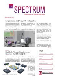
The Sun in the Light of the Hα Hydrogen Line<br />
Frequently, gas eruptions occur in<br />
these regions of activity. These prominences<br />
radiate in the red light<br />
of the Hα line at 656.3 nm. Unlike<br />
sunspots, they cannot be observed<br />
in the entire visible range since<br />
they are literally outshone by the<br />
photosphere. Only during a total<br />
solar eclipse can the solar limb including<br />
prominences be observed<br />
for a few seconds. During such a<br />
phenomenon, it is actually possible<br />
to examine the chromosphere<br />
with the naked eye. The chromosphere<br />
is the gaseous layer of<br />
the sun, which is adjacent to<br />
the photosphere and is about<br />
2000 km thick. Compared<br />
to the solar radius of almost<br />
700,000 km, however, this is<br />
not much.<br />
Fig.1: Left: The photosphere of the sun in the green light of the<br />
visible range - image taken with a Baader Solar Continuum filter<br />
(535-545 nm) on 19 May 2022 from the astronomical observatory in<br />
Meckesheim, Germany Top right: Close-up of a large sunspot group<br />
in green light. Bottom right: Detailed image of the chromosphere in<br />
the light of the Hα line at 656.3 nm with the configuration from Fig.<br />
4. The filament-like structures in the region of activity, which are<br />
caused by the gas eruptions in the magnetic field of the sunspots,<br />
are clearly visible. The bright regions in between the sunspots (socalled<br />
solar flares) are regions that are particularly hot and active.<br />
The sun is our star in the daytime sky<br />
and, in addition to supplying us with<br />
light, heat and life, it also provides us<br />
with a number of spectacular phenomena<br />
that we can study with the<br />
help of special solar telescopes. In<br />
the visible light of electromagnetic<br />
radiation (at wavelengths of about<br />
400-780 nm), for instance, sunspots<br />
can be observed (see Fig. 1, left). These<br />
are regions of increased magnetic<br />
activity that inhibits the supply of<br />
heat via convection from the interior<br />
of the sun. As a result, these regions<br />
are about 1500°C cooler than<br />
the surrounding environment with<br />
a temperature of approx. 5000°C, the<br />
so-called photosphere, which is the<br />
lowest layer of the solar atmosphere.<br />
To be able to study prominences<br />
and other interesting<br />
phenomena of the chromosphere<br />
of the sun not only during<br />
a solar eclipse, refractors<br />
with special filters are widely<br />
used today: The brightness<br />
of the solar image is reduced<br />
by a block filter (bandpass<br />
filter). To isolate the Hα<br />
line, etalons are usually used,<br />
which eliminate most of the radiation<br />
in the visible light by destructive<br />
interference, only allowing wavelengths<br />
around 656 nm to pass (see<br />
Fig. 2).<br />
Fig. 3: The "solar tower" of Meckesheim Observatory:<br />
With the two telescopes on the right, overview images<br />
of the sun can be taken in the range 535-545 nm and<br />
in the light of the Hα line as well as in the light of the<br />
Ca K line at 393.4 nm. The three refractors on the left<br />
are equipped with QUARK eyepiece filters and allow<br />
simultaneous images to be taken in the light of Hα<br />
(656.3 nm), Na D2 (589.0 nm) and Mg I b2 (517.3 nm).<br />
By using different filters, special solar phenomena can<br />
be studied at different stages of development.<br />
At Meckesheim Observatory, the sun<br />
is observed regularly, since it has<br />
not yet been found out when, how<br />
and why all these phenomena in<br />
the solar atmosphere occur. Regular<br />
observation of the spatial and kinematic<br />
changes associated with solar<br />
phenomena can provide more data<br />
for testing physical models of complex<br />
magnetohydrodynamic processes,<br />
which might lead to a better<br />
understanding of the nature of our<br />
sun, which in many aspects is still<br />
mysterious.<br />
Some of the acquired data is uploaded<br />
to central databases of astronomical<br />
associations and are thus<br />
available to interested amateurs and<br />
scientists.<br />
Fig. 3 shows the observatory's so-called<br />
solar tower: an arrangement of<br />
five solar telescopes, enabling simultaneous<br />
images to be taken in four<br />
different bands in the visible range,<br />
with bandwidths from 0.04 to 10 nm.<br />
Fig. 2: Left: Overview image of the sun in Hα light - image taken on 19 May 2022 from Meckesheim observatory,<br />
using a Lunt solar telescope at 50 mm aperture and 350 mm focal length In order to make the faint prominences<br />
at the solar limb visible, the solar disk must be overexposed. Right: Detailed view of the prominence at 50 mm<br />
aperture and 350 mm focal length (top) and at 102 mm aperture and 3070 mm focal length - image taken with the<br />
configuration from Fig. 4. The resolution is much better, thus allowing detailed studies.<br />
Among others, an Hα QUARK eyepiece<br />
filter by Daystar is used This filter<br />
accommodates a 4.3x focal length<br />
Page 5<br />
4
Optics<br />
extension, a 12 mm block filter and<br />
a 21 mm etalon. To adjust the wavelength,<br />
the etalon is heated with 1.5<br />
A at 5 V via a power supply unit. An<br />
aperture system ensures stray light<br />
reduction and provides for high contrast.<br />
Fig. 4 shows the setup for detailed<br />
studies of activity regions in Hα<br />
light on a refractor with 102 mm<br />
aperture and 714 mm focal length.<br />
The imaging is done using a monochrome<br />
astro camera, in which a<br />
Sony IMX174LLJ CMOS chip is installed<br />
and that delivers up to 120<br />
frames per second. This allows air<br />
turbulence to be "frozen" to a large<br />
extent. Due to their higher resolution,<br />
monochrome cameras are preferred<br />
over color cameras.<br />
Investigations in the light of the Hα<br />
line show changes in prominences,<br />
filaments, and flares over time scales<br />
of just a few minutes, while noticeable<br />
structural changes in photospheric<br />
phenomena (e.g. sunspots)<br />
cannot be be detected before several<br />
hours have elapsed. For this reason,<br />
Hα observations are of particular interest.<br />
After more than 6 years of regular<br />
use, reduced contrast was observed<br />
in the imaging of activity regions of<br />
the chromosphere: Prominences on<br />
the solar disk, recognizable as dark<br />
filaments, were barely visible (see<br />
Fig. 5 above).<br />
The reason for this was found quickly:<br />
The manufacturer's recommendation<br />
to put a UV-IR filter in front of<br />
the QUARK filter in telescopes with<br />
an aperture of 80 mm and larger had<br />
not been not complied with consistently.<br />
We now hoped that the etalon<br />
had not been damaged. Starting<br />
from the assumption that only the<br />
Fig. 5: An Hα image before and after replacement of<br />
the block filter In the bottom picture, the numerous<br />
appearing structures characterizing the solar activity<br />
are clearly visible.<br />
block filter had been affected (see<br />
Fig. 6), we ordered a bandpass filter<br />
656FS02-12.5 from Quantum Design.<br />
Fig. 6: The sunlight enters the filter system of the Hα<br />
QUARK eyepiece filter via this 12 mm bandpass filter<br />
(block filter), thus providing for dramatically reduced<br />
heat generation.<br />
With a CWL of 656.3 nm +0.2/-0 nm, an<br />
HWB of 1.0 nm ±0.2 nm at a transmission<br />
of at least 45% and a blocking of<br />
at least OD4, this filter meets the requirements<br />
for correct operation of<br />
the eyepiece filter. After this simple<br />
retrofitting measure, we noted with<br />
relief that the contrast in the image<br />
was as good again as it had been in<br />
the early years (see Fig. 5 below). Now,<br />
a permanently installed UV/IR filter<br />
in the optical deflection system prevents<br />
premature deterioration of the<br />
eyepiece filter system.<br />
■ Dr. Gerhard Hirth<br />
■ Director of Meckesheim<br />
Observatory<br />
■ https://www.sternwartemeckesheim.de<br />
For more information, please visit<br />
our website.<br />
www.qd-europe.com<br />
Fig. 4: Optical configuration for spatial and kinematic studies of solar chromosphere phenomena. Via an optical<br />
deflection system, sunlight from the refractor is guided through the Daystar Hα QUARK eyepiece filter. Here,<br />
imaging is done using an astro camera connected to a notebook.<br />
Please contact us<br />
optics@qd-europe.com<br />
5 <strong>Spectrum</strong>, International edition 39| December 2022
Imaging/Optics<br />
Marana-X-11 – Larger Sensor for EUV and<br />
Soft X-Ray Applications<br />
Andor Technologies expands its<br />
portfolio with an uncoated, back-illuminated<br />
sCMOS camera for the<br />
soft X-ray range.<br />
Building on its success with the Marana-X,<br />
Andor Technologies has added<br />
a large-format chip for direct<br />
X-ray detection to the Marana platform.<br />
With a 32mm sensor diagonal,<br />
this camera option responds to<br />
calls for a larger field of view, coming<br />
from scientists working in X-ray/EUV<br />
tomography and higher harmonics<br />
generation application areas.<br />
Whereas in this energy range, slowly<br />
digitizing CCD cameras are usually<br />
still the option of choice, the Marana-<br />
X represents a significant technical<br />
advance especially for photon energies<br />
from 80eV to 1keV. In particular,<br />
its outstanding quantum efficiency<br />
coupled with deep thermoelectric<br />
cooling and low readout noise despite<br />
a high frame rate is unique. The<br />
Marana-X combines high sensitivity<br />
with high dynamics.<br />
Another major advantage of sCMOS<br />
– compared with CCD technology –<br />
is the electronic shutter. This means<br />
that there is no need to use a vacuum-compatible<br />
mechanical shutter<br />
to prevent "smearing" of the image<br />
during the readout process.<br />
For spectroscopic applications, data<br />
transmission to the PC can be optimized<br />
by vertical or even user-defined<br />
FPGA binning, as is the case with<br />
all cameras based on the Marana<br />
platform. The necessary data depth<br />
in such a scenario is enabled by the<br />
32-bit data format.<br />
Either a USB3 or a CoaXPress data<br />
interface may be used. This not only<br />
provides for easy integration of the<br />
experiment but also for reliable data<br />
integrity where measurement setups<br />
are connected over long distances.<br />
As Antoine Varagnat, Andor’s Business<br />
Manager for Physical Sciences,<br />
puts it:<br />
"Marana-X 11 is a terrific addition to<br />
our growing portfolio of high-performance<br />
cameras. This latest detector<br />
is super-fast and sensitive, while<br />
it also benefits from a high dynamic<br />
range and high quantum efficiency,<br />
making it the optimal solution for<br />
direct soft x-ray and EUV imaging.<br />
"With a drive to upgrade high energy<br />
physics sources worldwide, to higher<br />
fluxes and repetition rates, this innovative<br />
product will help scientists<br />
make the most of these advances."<br />
Please contact us<br />
imaging@qd-europe.com<br />
Web Portal for Inquiries for Andover Bandpass Filters<br />
Andover offers a wide range of<br />
standard bandpass filters. To make<br />
it easier for you to select the right<br />
filter, we have set up a web portal.<br />
Here, you can see all filters in a clear<br />
layout. To automatically narrow<br />
the selection of filters shown, users<br />
can choose the specifications they<br />
are looking for. In the detailed<br />
view, you can see all specifications<br />
at a glance, together with the individual<br />
filter curves.<br />
Thus, you can find the right filter<br />
with just a few clicks. Our automatic<br />
inquiry system will immediately<br />
forward your selection to the<br />
corresponding staff. We will then<br />
contact you and give you a quote.<br />
Please contact us<br />
optics@qd-europe.com<br />
6
Materials science/About us<br />
Strain Tuning in 2D Materials – Nature<br />
Various material properties, e.g. the<br />
Curie temperature, can be influenced<br />
by stretching and compressing<br />
the materials. The Curie temperature<br />
describes the temperature above<br />
which a ferromagnetic material loses<br />
its magnetization. An easy way<br />
that does not require a mechanical<br />
test setup is inducing strain via<br />
magnetostriction or application of<br />
a voltage.<br />
Makars Šiškins of the Steeneken<br />
Team at Delft Technical University<br />
has published a spectacular paper<br />
on this topic in the journal Nature.<br />
In the paper, he describes how the<br />
resonant frequency of a 2D membrane<br />
(Cr2Ge2Te6-CGT) near its Curie<br />
temperature can be manipulated<br />
over a wide range. Embedding of a<br />
heterostructure prevents buckling<br />
and wrinkling that would normally<br />
occur in CGT membranes. The<br />
team has developed a method for<br />
studying magnetic properties almost<br />
at the level of individual layers,<br />
without interactions with the<br />
substrate distorting the measurement.<br />
Thanks to to their low mass, high<br />
strength, and resonant frequency<br />
tunability, CGT membranes are promising<br />
candidates for sensor applications<br />
and nanoelectromechanical<br />
systems.<br />
The team used a cryostation by<br />
Montana Instruments for their<br />
work. Due to its powerful vibration<br />
isolation, this special optical cryostat<br />
with closed helium loop has a<br />
vibration level of only a few nanometers<br />
in the sample chamber.<br />
Source: npj 2D Materials and Applications<br />
(2022) 6:41<br />
Please contact us<br />
materials@qd-europe.com<br />
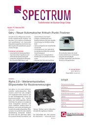
May I introduce myself?<br />
Hello, my name is Simon Wittner<br />
and since 2017 I am responsible<br />
for the product range of sample<br />
preparation for electron microscopy<br />
such as sputter coaters and critical<br />
point dryers in the service department<br />
of Quantum Design.<br />
Before I did my apprenticeship as<br />
a physics lab technician at Quantum<br />
Design (at that time still LOT-<br />
Quantum Design), I studied physics,<br />
education and educational<br />
sciences at the University of Koblenz-Landau<br />
on a teaching degree.<br />
Outside of work, I enjoy cycling a<br />
lot with my family in the nature of<br />
the Vorderer Odenwald.<br />
My tasks at Quantum Design include<br />
maintenance and repair of the<br />
offered devices of the company<br />
Quorum, installation and training<br />
at the customer's site in Germany<br />
and abroad, telephone and email<br />
support as well as finding individual<br />
solutions for the customer.<br />
You are welcome to contact me<br />
with your questions.<br />
Please contact us<br />
wittner@qd-europe.com<br />
7 <strong>Spectrum</strong>, International edition 39| December 2022
Imaging<br />
Chemical analysis of materials with high atomic numbers (Z)<br />
with our laboratory XAS system<br />
X-ray absorption spectroscopy (XAS)<br />
is a powerful method for studying<br />
chemical states and the coordinated<br />
environments of selected elements.<br />
XAS has been commercially<br />
available for laboratory use for several<br />
years. In this report, we demonstrate<br />
the exceptional performance<br />
of Sigray's QuantumLeap H2000 for<br />
high-energy XAS on a Zr sample at<br />
17998 eV.<br />
Many laboratory XAS systems have<br />
difficulty at energies >12 keV due<br />
The QuantumLeap H-series is optimized<br />
for a wide energy range from<br />
4.5 and 25 keV. In particular, the capacities<br />
in the high-energy range<br />
between 12 and 25 keV are of great<br />
importance for numerous nuclear<br />
applications as well as in catalysis.<br />
Absorption<br />
Zr foil<br />
QuantumLeap<br />
Synchrotron<br />
18000 18200 18400 18600<br />
Energy (eV)<br />
Fig. 2: Zr K-edge (17998 eV) XANES and EXAFS of a Zr<br />
film obtained with QuantumLeap (black), with comparative<br />
synchrotron data (red)<br />
Lanthanoide<br />
Actinoide<br />
Periodic Table of the Elements<br />
Fig. 1: Periodic table of the elements with highlighting of the elements with L- and K-edges between 12 and 25<br />
keV. K-edges are shown in green, L-edges in turquoise<br />
to increasing sagittal errors for Johann<br />
geometries at high energies.<br />
This is problematic because many<br />
important catalysts (Pt and Zr) and<br />
actinoids (U, Pu, Th, etc.) have L and<br />
K edges in the 12 to 25 keV range (see<br />
Fig. 1).<br />
Experiments and results<br />
We have used the QuantumLeap on<br />
a Zr foil with a thickness of 7.5 µm<br />
to demonstrate the capabilities offered<br />
by the system in high energy<br />
X-ray near edge absorption spectroscopy<br />
(XANES) and X-ray absorption<br />
fine structure (EXAFS) analysis<br />
Method<br />
Using intuitive software, the K-edge<br />
of Zr was selected from the periodic<br />
table of the elements.<br />
Fig. 2). The XAS data were processed<br />
and analyzed using the Athena and<br />
Artemis programs of the IFEFFIT package<br />
[1].<br />
Results and discussion<br />
Quantitative analysis of the Zr<br />
K-edge EXAFS was performed by<br />
fitting theoretical EXAFS spectra<br />
to the experimental data in<br />
R-space to obtain structural parameters<br />
(see Table 1). Included were<br />
the coordination number N, the<br />
bond length R, and the perturbation<br />
factor σ2. The scattering contributions<br />
from the shortest Zr-Zr<br />
bond of 3.21 Å are also included.<br />
The correlation between bond<br />
length and perturbation factors between<br />
synchrotron and QuantumLeap<br />
data is excellent. The error bars<br />
of all parameters are small, which<br />
emphasizes the reliability of the results.<br />
Summary<br />
We have demonstrated that la-<br />
Sigray's QuantumLeap X-ray absorption<br />
spectroscopy systems are the<br />
first XAS laboratory instruments<br />
with synchrotron-like capabilities.<br />
The QuantumLeap systems combine<br />
several patented features, e.g.<br />
■ ultra-bright X-ray sources, the<br />
imaging technology and<br />
■ the system design<br />
The system automatically<br />
selected the<br />
appropriate crystal<br />
– a cylindrically bent<br />
Johansson crystal Ge<br />
(800). An energy spectrum<br />
of 17.8-18.7 keV<br />
(wavenumber k=~13<br />
Å-1) was produced within<br />
seven hours (see<br />
8<br />
Strukturparameter Synchrotron Sigray QuantumLeap<br />
N 12 12<br />
R (Å) 3,23 ± 0,01 3,21 ± 0,01<br />
σ2 (Å2) 0,009 ± 0,001 0,012 ± 0,002<br />
Synchrotron and Sigray QuantumLeap Zr spectra (17.8 to 18.7 keV) were<br />
analyzed with Artemis. The results show excellent agreement with each<br />
other, demonstrating the exceptional high-energy XAS capabilities of the<br />
QuantumLeap<br />
Seite 9
Imaging/Crogenics<br />
boratory XAS using Sigray's<br />
QuantumLeap system can provide<br />
synchrotron-like results for<br />
high-energy XAS analysis. Using<br />
well-established software, measurements<br />
on a Zr foil were converted<br />
into quantitative results<br />
(bond length, coordination number,<br />
and local atomistic disorder).<br />
[1] B. Ravel and M. Newville, ATHENA,<br />
ARTEMIS, HEPHAESTUS: data analysis<br />
for X-ray absorption spectroscopy<br />
using IFEFFIT, Journal of Synchrotron<br />
Radiation 12, 537-541 (2005).<br />
Please contact us<br />
imaging@qd-microscopy.com<br />
Vibrations in OptiCool – A Closer Look<br />
Fig. 1<br />
OptiCool Vibrations on Positioner Stack<br />
OptiCool is an optical cryostat<br />
by Quantum Design, with superconducting<br />
magnets and closed<br />
helium circuit. The superconducting<br />
magnet requires a large cold<br />
head which, as a result of its design,<br />
emits significant vibrations.<br />
Thanks to a novel vibration isolation,<br />
the sample chamber is almost<br />
completely mechanically decoupled<br />
from the cold head. There<br />
are different ways to obtain a low<br />
vibration amplitude, as this article<br />
will show, using the X130 positioning<br />
system as an example. The<br />
amplitude alone is not sufficient<br />
to predict the performance of certain<br />
test setups.<br />
At the sample holder, called sample<br />
pod, the amplitude is just 10 nm<br />
peak-to-peak at 1.7 K base temperature.<br />
For most applications, a piezo<br />
positioning system is required for<br />
the sample pod. These positioners<br />
have a low resonant frequency<br />
and consequently vibrate strongly<br />
when excited.<br />
(a) horizontal displacement on positioner stack<br />
-4.4E-8<br />
Channel 2 - Position (m)<br />
-4.6E-8<br />
-4.8E-8<br />
-5E-8<br />
-5.2E-8<br />
-5.4E-8 8-9 nm<br />
-5.6E-8<br />
-5.8E-8<br />
-6E-8<br />
-6.2E-8<br />
-6.4E-8<br />
-6.6E-8<br />
-6.8E-8<br />
0 2 4 6 8 10 12 14 16 18 19.268<br />
Time (s)<br />
(b) vertical displacement on positioner stack<br />
5.03478E-8<br />
4.9E-8<br />
4.8E-8<br />
4.7E-8<br />
4.6E-8<br />
4.5E-8<br />
Channel 2 - Position (m)<br />
1.5 nm<br />
4.4E-8<br />
4.30435E-8<br />
5.169 5.5 6 6.5 7 7.5 8 8.5 9 9.237<br />
The X130 positioning system consists<br />
of two ANPx311/RES/LT/HV piezos<br />
(X and Y) and an ANPz102/RES/<br />
LT/HV (Z) by Attocube. For measuring,<br />
a SmarAct PicoScale laser interferometer,<br />
set to a bandwidth of 153<br />
Hz, was used.<br />
Figure 1 shows the timedependent<br />
amplitude in<br />
(a) horizontal and (b) vertical<br />
directions. The peakto-peak<br />
amplitude is just<br />
8-9 nm horizontally and<br />
1.5 nm vertically. These are<br />
the same values as those<br />
that are measured directly<br />
on the surface of the sample<br />
pod. This shows that,<br />
OptiCool<br />
despite the positioning system, the<br />
vibrations are not stronger. This is<br />
due to the low forces acting on the<br />
sample pod. A low amplitude can<br />
be achieved either by minimizing<br />
the acting forces and/or by a design<br />
with high stiffness, which means<br />
high resonant frequency. The fact<br />
that the low stiffness of the piezos<br />
does not negatively affect performance<br />
shows clearly that hardly<br />
any kinetic energy is transferred<br />
from the cold head to the sample<br />
pod. It is thus not necessary to use<br />
a design with high stiffness. Accordingly,<br />
this also applies to all hardware<br />
that is installed on the sample<br />
pod in connection with the experiment<br />
(e.g. sample holder or positioning<br />
system).<br />
Please contact us<br />
cryo@qd-europe.com<br />
9 <strong>Spectrum</strong>, International edition 39| December 2022
Cryogenics/Optics<br />
Recirculating cryocooler for "wet" cryostats<br />
Temperature (K)<br />
2.60<br />
2.55<br />
2.50<br />
2.45<br />
2.40<br />
2.35<br />
2.30<br />
2.25<br />
The recirculating cryocooler from<br />
Janis release “wet” cryostats from<br />
their dependency on liquid helium.<br />
Janis RGC4 series combines the advantages<br />
of cryo systems with open<br />
and closed cooling cycles.<br />
Base temperature ST-500 microscopy cryostat<br />
cooled by the RGC4 system<br />
0 50 100 150 200 250<br />
Time (h)<br />
Instead of cooling the samples directly<br />
through the cold head of the<br />
cryocooler, a secondary cooling cycle<br />
is set up and the cold head of a<br />
classic “wet” cryostat is cooled. This<br />
has several advantages:<br />
■ Same flexibility and convenience<br />
as a continuous-flow cryostat<br />
without liquid helium<br />
■ Quick sample change without<br />
warming up the RGC4 cooler<br />
■ Outstanding thermal performance<br />
■ Low vibration<br />
Pulse tube and GM coolers are available<br />
with 1 to 2W at 4.2 K. The system<br />
also includes a gas handling system<br />
and dry scroll pump for gas circulation.<br />
Compatible cryostats are:<br />
■ optical ST-100<br />
■ non-optical ST-200<br />
■ compact ST-300<br />
for use in a magnet<br />
■ UHV configuration ST-400 and<br />
■ microscopy configuration ST-500<br />
and the ST-500 based probe<br />
station<br />
Please contact us to discuss whether<br />
your cryostat from Janis or a third<br />
party provider is compatible with<br />
the recirculating cryocooler.<br />
Please contact us<br />
cryo@qd-europe.com<br />
Autonomous vehicles – Optical filters for LiDAR applications<br />
LiDAR is a sensing method that<br />
detects objects and maps their<br />
distances by sending an optical<br />
pulse at 905 nm or 1550 nm to the<br />
target and measuring the reflected<br />
return signal. Since conventional<br />
LiDAR system architectures use dedicated<br />
transmit and receive apertures,<br />
the resulting package has a<br />
relatively large footprint. However,<br />
leveraging polarization techniques<br />
can miniaturize the size of<br />
the optical subsystem. In addition,<br />
LiDAR systems routinely utilize<br />
narrow-band pass filters in both<br />
the transmitted and receiving<br />
path to improve the system signalto-noise<br />
ratio.<br />
Andover Corporation's self-reliant<br />
manufacturing approach places us<br />
in the optimal position to quickly<br />
provide customized prototypes of<br />
polarizing beamsplitters with unique<br />
angular performance characteristics<br />
to meet your LiDAR needs.<br />
With our 15 coating chambers, we<br />
can offer coating solutions from<br />
the UV range down to 15 µm. We<br />
also provide in-house manufacturing<br />
for coating fixtures, customized<br />
mounts, cutting, coring, shaping<br />
and polishing for a vast array<br />
of substrate materials.<br />
We provide standard bandpass filters<br />
that work with the common<br />
laser wavelengths used with most<br />
LiDAR systems, including 532 nm,<br />
905 nm, 1064 nm, and 1550 nm.<br />
This enables Andover Corporation<br />
to support both the development of<br />
new products and the production of<br />
optical sensors for the automotive<br />
industry. We offer customized engineering<br />
to provide superior and<br />
cost-effective solutions. Our extensive<br />
experience with image-quality<br />
bandpass filters, broadband AR coatings<br />
and polarizing beam splitters<br />
makes us an ideal partner for supplying<br />
the automotive industry with<br />
optical sensors. Our vertically integrated<br />
factory with in-house coating,<br />
manufacturing, optical assembly<br />
and testing capabilities can provide<br />
customized solutions at shorter<br />
lead-times.<br />
Please contact us<br />
optics@qd-europe.com<br />
10
Spectroscopy<br />
Spectroscopy with Fast Repetition Rates<br />
Photosynthesis in plants is the subject<br />
of intensive research. The absorption<br />
of light and its conversion<br />
into energy takes place in accordance<br />
with molecular mechanisms in<br />
pigments or the so-called light-collecting<br />
complexes. Understanding<br />
them is not only a benefit with regard<br />
to our knowledge in the field of<br />
biology, but also helps us with a view<br />
to developing efficient methods of<br />
energy production from sunlight.<br />
A distinction is made between electronic<br />
excitation processes in single<br />
molecules and collective excitations<br />
in aggregated molecules. In the close<br />
surroundings of the pigments, new<br />
electronic energy states are generated,<br />
with allowed and non-allowed<br />
transitions. They are coupled to intra-<br />
and intermolecular vibrations.<br />
These are the cause of the extremely<br />
fast processes on the femtosecond<br />
scale that can be observed. To investigate<br />
these processes, methods<br />
have been developed that enable<br />
changes to be detected in the optical<br />
spectrum of the molecules. In parallel,<br />
ever shorter laser pulses have<br />
become possible, which allows such<br />
phenomena to be studied more closely.<br />
As the time scales of molecular<br />
processes are so short, the Heisenberg<br />
Uncertainty Principle cannot<br />
be ignored, according to which time<br />
and energy cannot be determined<br />
simultaneously with any desired resolution.<br />
2D spectroscopy is the result<br />
of an evolution of pump-probe<br />
spectroscopy, in which information<br />
Andor Marana sCMOS Camera<br />
about the occupation and<br />
transition rates of electronic<br />
energy levels is obtained<br />
at different times. In<br />
this context, "two-dimensional"<br />
means plotting the<br />
signal as a function of the<br />
frequencies of excitation<br />
and emission. There are<br />
several methods based<br />
on this technology, which<br />
are well described in the<br />
publication which is the<br />
basis of this article (1). A<br />
common feature of some of these<br />
methods is that they require spectra<br />
to be recorded at high repetition<br />
rates. Depending on the method of<br />
choice, the spectral information<br />
may be hidden as a minimal variation<br />
on a high background. Making<br />
these weak signals visible requires a<br />
detector with a high dynamic range,<br />
the ratio of pixel capacitance to<br />
readout noise. CCD detectors often<br />
reach their limits here, since the<br />
readout noise (in the denominator)<br />
increases with increasing speed. Increasingly,<br />
sCMOS cameras can be<br />
used as an alternative. They combine<br />
high readout rates with very low<br />
readout noise. Meanwhile, CMOS<br />
sensors with large pixel sizes are<br />
available, in which dynamics, noise<br />
and sensitivity are combined in an<br />
ideal manner. Let us present you<br />
two cameras of this type that have<br />
proven useful for 2D or pump-probe<br />
spectroscopy. The ZYLA-5.5 sCMOS<br />
(Andor Technology) is capable of recording<br />
narrow, 8-lines<br />
spectra at up to<br />
27000 Hz with 15 bit<br />
intensity resolution.<br />
The Marana sCMOS<br />
cameras (Andor Technology)<br />
with their<br />
higher quantum efficiency<br />
enable rates<br />
of up to 11655 Hz<br />
with comparable line<br />
counts and external<br />
triggering. In the<br />
multitrack mode, it<br />
is possible to capture<br />
Principle of 2D spectroscopy. From (1)<br />
spatially separated spectra almost<br />
simultaneously in rapid succession.<br />
The fastest possible recording rate<br />
depends on the number of lines and<br />
their spacing on the sensor. Thus,<br />
several thousand Hz are possible<br />
even for two tracks. As the binning<br />
of CMOS pixels would exceed the 16<br />
bit scale of 65536 AD counts, FPGA<br />
preprocessing has been implemented,<br />
which transfers the added-up<br />
intensity values in 32 bit format to<br />
the computer.<br />
With these features, Andor sCMOS<br />
cameras in conjunction with spectographs<br />
of the Kymera and Shamrock<br />
series provide for a versatility<br />
far beyond that of similar cameras<br />
by other manufacturers. If you are<br />
interested in more information,<br />
please feel free to ask us or discuss<br />
your application with one of our<br />
product managers from the Spectroscopy<br />
& Imaging department.<br />
(1) A. Gelzinis, Ramūnas Augulis, Vytautas<br />
Butkus, Bruno Robert, Leonas<br />
Valkunas; BBA - Bioenergetics 1860<br />
(2019) 271–285<br />
Please contact us<br />
spectroscopy@qd-europe.com<br />
11 <strong>Spectrum</strong>, International edition 39| December 2022
About us<br />
Headquarters Pfungstadt: Progress is being made<br />
For a long time it felt like nothing<br />
was happening on our construction<br />
site for the new headquarters in<br />
Pfungstadt. There were even rumors<br />
of an alleged construction stop. But<br />
sometimes it's the bureaucracy that<br />
gets in the way. After about seven<br />
months of waiting, work on the office<br />
building could finally begin.<br />
The necessary ground work had<br />
already been completed for some<br />
time.<br />
Now things are finally moving forward<br />
and our new office space is taking<br />
shape in the form of the floor<br />
slab. At 3 o'clock in the morning the<br />
work started. Eight trucks shuttled<br />
the concrete from Gernsheim to the<br />
construction site. A total of approximately<br />
65 tons of steel for the reinforcement<br />
and 260 m³ of concrete<br />
were used. The dimensions of the<br />
future office complex are now already<br />
clearly visible. The warehouse<br />
will later join the office building in<br />
the southwest.<br />
We are pleased with the great progress<br />
on our construction site and<br />
can hardly wait to move into the<br />
new headquarters in 2023.<br />
Please contact us<br />
spectrum@qd-europe.com<br />
12
Life science<br />
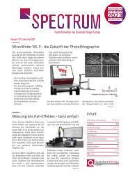
Factors Influencing the Stability of the QCM-D Baseline<br />
Baseline stability is very important<br />
for obtaining high-quality and reproducible<br />
QCM-D data and measuring<br />
them with high-sensitivity. Here are<br />
some factors that will help you optimize<br />
baseline stability in your QCM-D<br />
measurements.<br />
Bubble formation during measurement<br />
Gas bubbles may form on the surface<br />
of the sensor when using a liquid that<br />
has not been properly degassed. Such<br />
bubbles will have an influence both<br />
on frequency and on dissipation.<br />
E.g., gas solubility in water decreases<br />
with rising temperature. When working<br />
at a sensor temperature above<br />
room temperature and water-based<br />
buffer is introduced into the measuring<br />
chamber, then there is a risk of<br />
bubble formation. Note that the risk<br />
of bubble formation generally increases<br />
as the salt concentration of an<br />
aqueous solution decreases.<br />
Solution: Use degassed liquids only<br />
or make sure that the gas solubility<br />
of the liquid is not reduced during<br />
measurement.<br />
Temperature variations<br />
a) Measurement with oscillating<br />
quartz crystal microbalances is very<br />
sensitive to temperature variations.<br />
The QSense measuring chambers<br />
have a very good temperature stabilization,<br />
but large temperature<br />
variations in the environment or in<br />
the sample solution may not be fully<br />
compensated. A change in temperature<br />
will change viscosity and density<br />
of a liquid and thus, f and D will<br />
change, too.<br />
Solution: Make sure the temperature<br />
controller is switched on. Ensure<br />
a constant temperature in the environment<br />
of the instrument and<br />
provide for sufficient and constant<br />
air circulation. Protect the<br />
instrument against direct<br />
sunlight or air currents (e.g.<br />
from an air conditioner).<br />
b) Unwanted resonant modes<br />
can interfere with the<br />
main resonance. These modes<br />
are usually very temperature<br />
dependent.<br />
Solution: Change the set temperature<br />
slightly to get away<br />
from the mode interference.<br />
After a system switch-on,<br />
insertion of modules or a<br />
change of the temperature<br />
setting, it will take some<br />
time before the entire chamber<br />
and the modules reach<br />
a temperature equilibrium<br />
- please bear that in mind.<br />
If possible, wait at least 30<br />
minutes (but anyway until<br />
the signal is steady) before starting<br />
a measurement after such an event.<br />
Reactions on the sensor back<br />
The back side of the sensor is just<br />
as sensitive to surface reactions as<br />
the front side. Both surfaces influence<br />
the QCM-D signal in the same<br />
way. For example, a variation in the<br />
(relative) humidity on the back of<br />
the sensor (e.g., due to a leakage or a<br />
large temperature shift) can potentially<br />
change the amount of water<br />
adsorbed on the back and thus affect<br />
f and D. Note that the air space<br />
on the back of the sensor is in contact<br />
and exchange with the ambient<br />
environment through the holes for<br />
the spring-loaded contacts.<br />
Make sure the dew point of the air<br />
around the platform (which is in<br />
contact with the back of the sensor)<br />
is significantly higher than the<br />
measuring temperature.<br />
For additional tips and guidance, refer<br />
to Biolin Scientific's guide "How<br />
to optimize the QCM-D baseline stability"<br />
at www.biolinscientific.com<br />
Please contact us<br />
nano@qd-europe.com<br />
13 <strong>Spectrum</strong>, International edition 39| December 2022
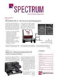
Materials science<br />
MicroWriter – Our Direct-Writing Lithography System with<br />
Clever Features<br />
This basic principle is now extended<br />
by various options for the writing<br />
quality - irrespective of the resolution<br />
used. The feature "Automatic Pixel<br />
Smoothing" gives users the option<br />
to decide about the quality of the<br />
edges of the structures to be written.<br />
Fig. 3<br />
Fig. 1<br />
High resolution and fast writing -<br />
these are the typical requirements<br />
for a direct-writing photolithography<br />
system. However, high resolution<br />
compromises writing speed<br />
and vice versa. For this reason, the<br />
developers of our MicroWriter systems<br />
have put much thought into<br />
the question of how these two requirements<br />
can be reconciled as<br />
far as possible. Even the first generation<br />
of the MicroWriter allowed<br />
the user to select different resolutions<br />
for different objects. The highest<br />
resolution is selected only for<br />
those objects for which high resolution<br />
is really important, whereas<br />
a lower resolution is chosen for<br />
objects for which high resolution<br />
is not an absolute must, which comes<br />
with the benefit of a higher<br />
writing speed.<br />
Fig. 2<br />
The example in figure 1 shows the<br />
difference. The gap width of the coil<br />
is 2.5 µm and the resolution of writing<br />
was 1 µm. The roughness of the<br />
edges can typically be observed in<br />
the outstanding range of 30 nm. If<br />
this feature is not used, the writing<br />
speed increases dramatically, however,<br />
at the expense of edge quality.<br />
Fig. 4<br />
The second important feature is<br />
the so-called "Virtual Mask Aligner",<br />
which offers the possibility of placing<br />
the object to be written over the<br />
optical image of the sample surface.<br />
This is very helpful<br />
if structures<br />
to be written<br />
are to be aligned<br />
with structures<br />
that are already<br />
on the surface. A<br />
typical example<br />
are contact pads<br />
for e.g. graphene<br />
or 2D materials.<br />
Figure 2 shows<br />
how this looks<br />
in the software,<br />
while figure 3 is<br />
an actual result<br />
from one of our<br />
customers (courtesy<br />
of UGC-DAE Consortium for<br />
Scientific Research, Indore, India).<br />
The last feature is the "Wide Field<br />
Viewer". This feature allows you to<br />
quickly and easily generate a larger<br />
overview image of the sample surface.<br />
The system automatically circles<br />
the starting point, capturing one<br />
optical image at a time. Each further<br />
image will be stitched together<br />
to create an ever larger overview<br />
image. This feature can be used, e.g.,<br />
to find alignment markers or to<br />
look at already written structures<br />
for a first inspection.<br />
Please contact us<br />
materials@qd-europe.com<br />
14
Materials Science<br />
The Lock-In Amplifier – NOT a Closed Book<br />
The lock-in amplifier was developed<br />
in 1941, and has ever since<br />
undisputedly occupied a very<br />
important place when it comes<br />
to sensitive electrical measurements.<br />
But "lock-ins" are also<br />
used in other areas: E.g., in a VSM<br />
magnetometer for sensitive magnetic<br />
measurements such an<br />
amplifier is an essential part of<br />
the measuring electronics.<br />
A lock-in amplifier "equalizes"<br />
frequencies, so, as far as electrical<br />
measurements are concerned, we<br />
always refer to AC applications.<br />
AC means "alternating current",<br />
and an example of what can be<br />
measured is AC resistance. In its<br />
most simple form, the lock-in is<br />
an AC voltmeter that measures<br />
at a fixed frequency only. The signal<br />
from the AC current source<br />
is supplied to the lock-in, passing<br />
through the sample, but it is also<br />
supplied directly as a reference<br />
signal (of course, it would also be<br />
possible to generate the reference<br />
signal internally).<br />
M81<br />
Advantages of the lock-in technology:<br />
The amplitude can be<br />
low, and background noise and<br />
other interfering signals or frequencies<br />
can be removed, since,<br />
in a simplification, we are only<br />
looking at this one frequency. In<br />
the figure, the basic structure of<br />
a lock-in system is shown. The<br />
components highlighted in gray<br />
form part of the DSP (digital signal<br />
processor). The DSP is the heart<br />
of any modern lock-in instrument.<br />
From the figure, it also becomes<br />
clear that in order to really understand<br />
the technology, one has<br />
to have a closer look e.g. at the<br />
function and mode of action of<br />
the various filters. But for those<br />
of our readers who simply want<br />
to make sensitive electrical measurements,<br />
listen: Lake Shore's<br />
M81 measuring system features<br />
an integrated lock-in amplifier<br />
that can easily be activated and<br />
deactivated!<br />
Learn more about the lock-in<br />
technology and gain background<br />
knowledge, including about filters,<br />
noise and different types of<br />
noise, as well as precision and<br />
accuracy, by reading Lake Shore<br />
Cryptotronics' white paper "The<br />
Lock-In Amplifier Explained and<br />
Reimagined", which we will be<br />
happy to send you on request<br />
free of charge, either by e-mail or<br />
as a printout.<br />
For more information, please visit<br />
our website.<br />
www.qd-europe.com<br />
Please contact us<br />
materials@qd-europe.com<br />
A<br />
B<br />
AC or DC<br />
Coupling<br />
A or<br />
A-B<br />
AC gain<br />
Inputfilter<br />
Inputfilter<br />
Outputfilter<br />
X signal<br />
in-phase signal<br />
ext. Input reference<br />
Output Reference<br />
PLL<br />
local<br />
Oscillator<br />
Reference<br />
Phaseshift<br />
Harmonics-<br />
Generator<br />
90° phase<br />
shift<br />
Outputfilter<br />
Y signal<br />
phase shifted signal<br />
quadrature signal<br />
15 <strong>Spectrum</strong>, International edition 39| December 2022
Materials science<br />
European Headquarters<br />
Quantum Design GmbH<br />
Im Tiefen See 58, 64293 Darmstadt, Germany<br />
Phone +49 6151 8806-0, Fax +49 6151 8806 920<br />
E-mail spectrum@qd-europe.com<br />
www.qd-europe.com<br />
Quantum Design BeNeLux<br />
Meerstraat 177<br />
B-1850 Grimbergen, Belgium<br />
Phone +32 2 3084324<br />
Mobile +32 495797175<br />
E-mail struyve@qd-europe.com<br />
Quantum Design Czech Rep. and Slovak. Rep.<br />
Krivoklatska 37, 199 00 Praha 9, Czech. Rep.<br />
Phone +420 607 014 278, Fax +420 24 1046850<br />
E-mail czechia@qd-europe.com<br />
Quantum Design France SARL<br />
Bâtiment Mac Kinley, 1, avenue de l’Atlantique,<br />
91940 Les Ulis, France<br />
Phone +33 1 69194949, Fax +33 1 69194930<br />
E-mail france@qd-europe.com<br />
Quantum Design Iberia<br />
(for Portugal and Spain)<br />
Roca i Roca, 45, 08226 Terrassa (Barcelona), Spain<br />
Phone and Fax +34 937349168<br />
E-mail boira@qd-europe.com<br />
Quantum Design s.r.l., Italia<br />
Via Francesco Sapori, 27<br />
00143 Roma, Italy<br />
Phone +39 06 5004204, Fax +39 06 5010389<br />
E-mail italy@qd-europe.com<br />
Quantum Design Magyarország<br />
Primet Méréstechnikai Kft<br />
Eszak u. 24, HU-1038 Budapest<br />
Phone and Fax +36 1 2402711,<br />
E-mail steinbach@qd-europe.com<br />
Quantum Design Nordic<br />
(for Denmark, Finland, Norway and Sweden)<br />
Roddarestigen 3, 182 35 Danderyd, Sweden<br />
Phone +46 8 41071791<br />
E-mail eriksson@qd-europe.com<br />
Quantum Design Przedstawicielstwo Polska<br />
Mikoów: tel.:+48 32 24457<br />
Fax: +48 32 4281169, kom.: +48 50 255112014<br />
pdluzewski@qd-europe.com lub<br />
Chorzów: tel.: +48 32 2482048<br />
Fax: +48 32 70 21 160, kom.: +48 51 5166893<br />
E-mail kowalczyk@qd-europe.com<br />
Quantum Design SRL<br />
(for Romania and Bulgaria)<br />
Str Ion Nistor Nr 4, et 1, M2E<br />
030041 Bucharest, Ro.<br />
Phone +40 75 50 39 900, Fax +40 31 7107156<br />
E-mail buiu@qd-europe.com<br />
Quantum Design AG Suisse<br />
Route du Roule 41, 1723 Marly, Switzerland<br />
Phone +41 21 8699033, Fax +41 21 8699308<br />
E-mail reinicke@qd-europe.com<br />
Quantum Design Turkey<br />
Phone: +90 544 741 99 97<br />
E-mail turkiye@qd-europe.com<br />
Quantum Design Ltd. UK and Ireland<br />
1 Mole Business Park, KT22 7BA Leatherhead,<br />
Surrey, United Kingdom<br />
Phone +44 13 72378822, Fax +44 13 72375353<br />
E-mail info@qd-uki.co.uk<br />
Quantum Design Russia<br />
(for Russia and Central Eurasia)<br />
Phone +7 495 938-1866 , Fax +7 495 938-1907<br />
E-mail academ@qd-europe.com<br />
New Enhanced Scratch Test Module for<br />
the NanoTest Vantage Platform 5<br />
MicroMaterials has revised and significantly<br />
enhanced the scratch and<br />
wear option of the NanoTest Vantage<br />
Indenter for Platform 5.<br />
The enhancements provide the ability<br />
to take advantage of the NanoTest's<br />
high lateral stiffness and<br />
thermal stability. The user has full<br />
control over loading, unloading<br />
and holding segments to perform<br />
scratch and wear tests with complex<br />
loading procedures. This opens up<br />
new types of experiments, such as<br />
abrasion simulations or pendulum<br />
wear tests.<br />
To perform wear tests directly, multiple<br />
parallel scratches can be generated<br />
in a single experiment run. In<br />
doing so, the software generates a<br />
random offset for the start position<br />
of each scratch.<br />
For detailed investigation of wear<br />
and fracture processes, analysis regions<br />
can be defined and the software<br />
then automatically calculates the<br />
mean and standard deviation for all<br />
measured parameters for each scan.<br />
Measured parameters include load<br />
and residual depth, friction force<br />
and coefficients, and six different<br />
surface roughnesses.<br />
The innovations in Platform 5 at a<br />
glance:<br />
■ User-defined multi-load loading<br />
option for single scratch and<br />
repeated scratch tests.<br />
■ Abrasion simulation<br />
■ Pendulum wear tests<br />
■ User-defined data density<br />
■ Data analysis and reporting:<br />
■ Multi-axis composite charts<br />
■ Improved compensation options<br />
■ Integrated microscopy and<br />
positioning<br />
■ Automatic analysis of surface<br />
roughness statistics. Depth,<br />
friction and ECR for user-defined<br />
regions<br />
■ Calculation of step height<br />
■ Test reports according to ISO/CEN<br />
17627<br />
More details and a case study<br />
can be found at: bit.ly/3zSNmuM<br />
Please do not hesitate to contact us<br />
if you have any questions regarding<br />
this or other modules in conjunction<br />
with NanoTest Vantage.<br />
Please contact us<br />
materials@qd-europe.com<br />
Follow us on LinkedIn:<br />
https://www.linkedin.com/<br />
company/quantum-design-europe<br />
Editor: Joachim Weiss, PhD<br />
Please note that not all products are available in every country.<br />
carbon neutral<br />
natureOffice.com | DE-617-226SY2T<br />
print production<br />
16