Spectrum E38

Create successful ePaper yourself
Turn your PDF publications into a flip-book with our unique Google optimized e-Paper software.
News from Quantum Design Europe<br />
Edition 38 | June 2022<br />
New energy discriminating detectors for<br />
soft and hard X-ray radiation<br />
Detectors based on CCD or CMOS<br />
sensors are measuring instruments<br />
for the incident radiation power.<br />
These image sensors made of silicon<br />
are excellently suited for highly<br />
sensitive detection of visible light,<br />
but also for parts of the invisible<br />
spectrum. They offer the scientist a<br />
variety of features such as high spatial<br />
resolution and high dynamic<br />
range. However, radiation sensors of<br />
this type have the disadvantage that<br />
they cannot detect photons as single<br />
events. However, this is particularly<br />
interesting and technically possible<br />
in the X-ray spectrum because<br />
the energy of one photon is large<br />
enough to generate several hundred<br />
excitons.<br />
Our newcomer ADVACAM from<br />
Prague (Czech Republic) and Espoo<br />
(Finland), respectively, fills this gap<br />
in the X-ray spectrum for the soft<br />
to hard energy range. ADVACAM<br />
started in 2013 as a spin-off from<br />
the Institute of Experimental and<br />
Applied Physics at the University<br />
of Prague. ADVACAM OY is a spinoff<br />
company of VTT Technical Research<br />
Centre of Finland. The companies<br />
are certified according to<br />
ISO 9001 standards. We are pleased<br />
to bring their products on board.<br />
The detectors are based on the Timepix<br />
or Medipix technology developed<br />
at CERN. The sensors are<br />
made of silicon or CdTe. They cover<br />
different energy ranges: silicon is<br />
used from 3 keV, CdTe from 5 keV.<br />
There are operation modes like<br />
photon counting, time over threshold<br />
and time of arrival.<br />
In addition to spatial and temporal<br />
resolution, they also enable<br />
energy discrimination of individual<br />
high-energy photons.<br />
The achievable energy resolution<br />
is given by material properties.<br />
Page 2<br />
New headquarters for<br />
Quantum Design Europe<br />
Quantum Design Europe will<br />
move to a new town<br />
After more than 50 years in Darmstadt,<br />
we thought it was time for a<br />
change. In less than two years, we<br />
will be operating from Pfungstadt,<br />
a small town only 10 km south of<br />
here.<br />
On an area of approx. 8500 m²,<br />
our new headquarters will boast<br />
2800 m² of state-of-the-art office facilities<br />
and approx. 1000 m² of warehouse<br />
space. We look particularly<br />
forward to spacious demo and training<br />
areas as a core element of our<br />
work and the support of our customers.<br />
The official permit to start construction<br />
was already granted in<br />
February of this year. Since then,<br />
Page 3<br />
Content<br />
About us 3, 12<br />
Cryogenics 3, 7-10, 12<br />
Electron microscopy 5<br />
Imaging 6, 10,<br />
Light & lasers 3<br />
Materials science 2, 4, 5, 8, 11,<br />
Optics 11<br />
Spectroscopy 2<br />
EUROPE
Spectroscopy/Materials science<br />
New energy-resolving detectors for soft and hard X-rays<br />
The detectors operate in list mode,<br />
in which a continuous list of entries<br />
containing this information is<br />
generated from the detector events.<br />
The principle is known from particle<br />
physics. The current Timepix3<br />
sensors allow a time resolution of<br />
1.6 ns without dead time at a count<br />
rate of up to 40 million events per<br />
second.<br />
The comprehensive Pixel Pro software<br />
supports the user in data acquisition<br />
and analysis. Their applications<br />
for Advacam's detectors<br />
include non-destructive fluoroscopy,<br />
X-ray imaging of tissue and<br />
animals, rock samples from geology,<br />
and crystal structure analysis<br />
using X-ray diffraction. Methods<br />
that require energy-resolving detectors<br />
for ions or even neutrons<br />
can use Advapix models for this<br />
purpose.<br />
Please contact us<br />
spectroscopy@qd-europe.com<br />
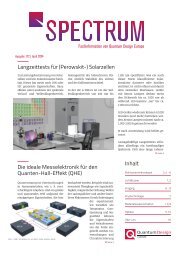
Quantum efficiency in photovoltaics<br />
Quantum efficiency in photovoltaics<br />
is the ratio of electrons in a<br />
photocurrent to the number of<br />
photons that hit, for example, a solar<br />
cell. Since no one wants to count<br />
individual electrons or photons,<br />
it is common to compare the component<br />
that is to be tested with a<br />
calibrated element. The unknown<br />
quantum efficiency QE is results<br />
from the following:<br />
QE=QE kal<br />
∙<br />
I mess<br />
I kal<br />
QE kal<br />
is the quantum efficiency of<br />
the calibrated component, and the<br />
quotient is the ratio of the two generated<br />
currents. This is subject to<br />
both cells being irradiated with the<br />
same luminous intensity. The image<br />
shows a typical QE measurement<br />
setup (here: on a photodiode). On<br />
the left side radiation of a specified<br />
wavelength (energy) is created. The<br />
chopper creates lighting packages<br />
of a determined frequency. On the<br />
right you can see an M81 with two<br />
current measurement pods. The<br />
main system M81-SSM entangles<br />
and measures the two currents (I mess<br />
and I kal<br />
) which occur at the photodiodes,<br />
with reference to the chopper<br />
frequency and phase.<br />
Compared to the classic measurement<br />
setup with two preamplifiers<br />
and two lock-in channels, this system<br />
not only saves hardware but<br />
also gains metrological flexibility.<br />
For example, the M81 allows DC<br />
measurements like current/voltage<br />
characteristic (IV) curves or creating<br />
a bias (by using additional pods, if<br />
necessary). In the table, you will find<br />
the specifications of the combination<br />
M81-SSM with the current measure<br />
module CM.<br />
In principle, quantum efficiency<br />
can also be measured on other optoelectronic<br />
components, like phototransistors,<br />
photomultipliers, photocathodes,<br />
solar cells and image<br />
intensifiers.<br />
M81 CM-10 Current measure<br />
module<br />
■ Frequency: DC to 100 kHz<br />
■ Best sensitivity: 10 fA<br />
■ Max. range: 100 mA<br />
■ Bias voltage: +/-10 V<br />
Instrumentation of an sEQE measurement using an M81-SSM with CM-10 module. Here, the M81 can be configured to perform<br />
both DC-I-V sweeps and lock-in detection of the AC photocurrent occurring in the device.<br />
Please contact us<br />
materials@qd-europe.com<br />
2
About us/Light&Lasers<br />
The new headquarters of Quantum Design Europe<br />
large amounts of scrubs have been<br />
taken away. After that, almost<br />
2000 m³ must be carried away, before<br />
we can start constructing the<br />
actual buildings.<br />
We symbolically broke the ground in<br />
February at perfect weather conditions:<br />
Under blue skies and sunshine,<br />
we talked about the new site, construction<br />
plans, and last but not least<br />
- future neighbors.<br />
With sparkling white wine, we toasted<br />
with city council Horst Knell,<br />
Christine Rühl from City Development<br />
Pfungstadt and the architect<br />
in charge Jörk Zimmermann to the<br />
beginning of a bright future.<br />
We look forward to the coming construction<br />
phases.<br />
If you are curious – you can check<br />
out our website for information on<br />
the development.<br />
www.qd-europe.com/new-building/<br />
Please contact us<br />
spectrum@qd-europe.com<br />
Good old state-of-the-art: Laser Power Meters from Macken<br />
For more than 30 years, Macken has<br />
been our team partner when it comes<br />
to laser power meters. Classic<br />
power meters (aka “bones”) are still<br />
in demand by many users. They provide<br />
fast and easy measurements at<br />
little cost and effort.<br />
In the meantime, new, digital power<br />
meters have entered the market and<br />
with help of license-free software,<br />
measurements can also be taken<br />
and stored online.<br />
NIST-traceable calibrations and<br />
continuous calibration services are<br />
offered and recommended to ensure<br />
reproducible measurements.<br />
In addition, we still offer Macken’s<br />
well-established image plates (regular<br />
and water-cooled for high powers)<br />
to align for example beamline<br />
systems in laser plants. The image<br />
plates are also quick and easy to use.<br />
Laser spectrum analyzers are critical<br />
in the inspection of laser<br />
resonators. This unique grating<br />
spectrograph visualizes all laser<br />
transactions of a CO 2<br />
laser at the<br />
same time. All analyzers are calibrated<br />
in both wavelength and rotational<br />
line designation to allow easy<br />
identification of 140 possible laser<br />
transitions between 9.1 and 11.3 µm.<br />
These transitions are visually displayed<br />
using a UV-excited, thermally<br />
sensitive screen which darkens in<br />
the area struck by the IR laser beam.<br />
Laser spectrum analyzers for CO,<br />
HF and DF lasers are standard.<br />
Analyzers for N 2<br />
O and CS 2<br />
, CO 2<br />
carbon<br />
isotope and broadband wavelengths<br />
are available upon request.<br />
The spectrum analysis screen has<br />
a response time of 1/4 seconds and<br />
allows the instrument to resolve all<br />
the CO 2<br />
rotational lines. Model 16-A<br />
is light, portable and can easily be<br />
integrated into laboratory setups.<br />
Please contact us<br />
lightsources@qd-europe.com<br />
3 <strong>Spectrum</strong>, International edition 38| June 2022
Materials science<br />
IR-VASE at the Institute of Physical Chemistry of the<br />
Romanian Academy of Sciences in Bucarest<br />
Short overview of the task at hand<br />
with IR spectral ellipsometry<br />
By Dr. Mariuca Gartner, Head of Laboratory<br />
Since August 2008, the<br />
Institute of Physical<br />
Chemistry has had<br />
an Infrared Spectroscopic<br />
Ellipsometer<br />
(IR - VASE) – built by J.<br />
A. Woollam (now available in updated<br />
configuration). This is still a unique<br />
system in Romania. It has mainly<br />
been used to investigate optical, chemical,<br />
and vibrational properties of<br />
thin films obtained by chemical (solgel)<br />
and physical (sputtering, PLD)<br />
methods. These properties are analyzed<br />
as function of technological<br />
parameters of deposition (substrate,<br />
annealing, dopant concentrations<br />
and others).<br />
The IR-VASE based studies (carried<br />
out over 1.7-30 µm wavelength range)<br />
offer increased sensitivity over FTIR<br />
spectroscopy and yield quantitative<br />
values for the optical constants n,<br />
and k. This technique has excellent<br />
sensitivity in regards to thin layer<br />
thickness and doping concentration,<br />
which is not seen using UV-VIS wavelengths.<br />
Compared with FTIR or Raman, IRSE<br />
can offer more information from<br />
a single measurement, like optical<br />
constants and chemical composition.<br />
IR-VASE, Mark II<br />
Our institute performs the<br />
following studies:<br />
1. The vibrational bands‘<br />
assignation can be made<br />
very quickly, directly from<br />
experimental IR spectra<br />
(from the inflexion points<br />
of the Ψ and Δ spectra)<br />
without any calculations<br />
[1]. Raman assignations<br />
confirm those obtained<br />
by IR-VASE.<br />
2. The analysis of the dielectric<br />
functions evaluated<br />
from the IR-VASE spectra<br />
showed the formation<br />
of thin layers in nitrogen<br />
plasma implanted Si,<br />
which is identified as oxynitride<br />
with low N concentration.<br />
The inclusion<br />
of N atoms in the Si-O network<br />
in different configurations<br />
was analyzed by<br />
IRSE, and the results were<br />
confirmed by XPS and VIS-<br />
SE spectroscopy [2].<br />
3. The vibrational spectra of the<br />
phonon modes E1(TO) and A1(LO)<br />
of different films (deposited on<br />
other substrates and by various<br />
preparation techniques) were analyzed<br />
[3-5]<br />
4. If we unify the data obtained<br />
from UV-VIS-NIR (0.193 - 1,7 µ) range<br />
with these from IR range (1.7-33<br />
µ), we can have a large image of the<br />
optical constants and of the transmission<br />
on a very large scale from<br />
UV to IR (0.193 to 33µ) [6, 7].<br />
References:<br />
1. M. Nicolescu, M. Anastasescu, J.M.<br />
Calderon-Moreno, A.V. Maraloiu,<br />
V.S. Teodorescu, S. Preda, L. Predoana,<br />
M. Zaharescu, M. Gartner,<br />
“Optical, microstructural and vibrational<br />
properties of sol–gel ITO<br />
films“, Optical Materials 114 (2021)<br />
110999<br />
Optical constants of ITO deposited on silicon by sol-gel process<br />
2. M. Gartner, A. Szekeres, S. Alexandrova,<br />
P. Osiceanu, M. Anastasescu,<br />
M. Stoica, A. Marin, E. Vlaikova, E.<br />
Halova, “Infrared ellipsometry as<br />
an investigation tool of thin layers<br />
grown into plasma immersion N+<br />
implanted silicon“, Appl.Surf.Sci.,<br />
258, 7195– 7201(2012)]<br />
3. Nitrogen Amount on the Microstructural<br />
and Optical Properties of<br />
Thin r.f.-Sputtered ZnO Films Treated<br />
by Rapid Thermal Annealing“,<br />
Appl.Surf.Sci., 261, 815– 823 (2012)<br />
4. S. Bakalova, A. Szekeres, M. Anastasescu,<br />
M. Gartner, L. Duta, G. Socol,<br />
C. Ristoscu, I.N Mihailescu, „VIS/<br />
IR spectroscopy of thin AlN films<br />
grown by pulsed laser deposition<br />
at 400°C and 800°C and various N2<br />
pressures“, Journal of Physics: Conference<br />
Series 514, 012001(2014)<br />
5. N. Dulgheru, M. Stoica, J.M. Calderon-Moreno,<br />
M. Anastasescu, M.<br />
Page 5<br />
4
Materials science/Electron microscopy<br />
Nicolescu, H. Stroescu, A. Szekeres,<br />
M. Gartner, „Influence of compositional<br />
variation on the optical and<br />
morphological properties of Ge-Sb-<br />
Se films for optoelectronics application“,<br />
Infrared Physics and Technology<br />
93 (2018) 260–270<br />
6. M. Nicolescu, M. Anastasescu, S.<br />
Preda, J. M. Calderon-Moreno, H.<br />
Stroescu, M. Gartner, V .S. Teodorescu,<br />
A.V. Maraloiu, V. Kampylafka, E.<br />
Aperathitis, M. Modreanu, “Surface<br />
topography and optical properties<br />
of nitrogen-doped ZnO thin films<br />
formed by radio frequency magnetron<br />
sputtering on fused silica substrates”,<br />
J. Optoelectron. Adv. Mater, 12<br />
(6), 1343-1349 (2010)<br />
7. H.Stroescu, M.Anastasescu, S.Preda,<br />
M.Nicolescu, M.Stoica, N.Stefan,<br />
E. Aperathitis, M. Modreanu, M. Zaharescu,<br />
M. Gartner, „Influence of<br />
thermal treatment in N2 atmosphere<br />
on chemical, microstructural and<br />
optical properties of ITO and ITO:<br />
N sputtered thin films”, Thin Solid<br />
Films, 541,121-126 (2013)<br />
Please contact us<br />
materials@qd-europe.com<br />
AFSEM nano – Correlative AFM- & SEM analysis now in Stanford<br />
As kind of an early Christmas present,<br />
our AFSEM nano system was<br />
installed at the University of Stanford<br />
in the beginning of December.<br />
Prof. Dr. Fritz Prinz and his group<br />
for nanoscale prototyping work on<br />
fundamental issues around energy<br />
conversion and storage in the nanoscale<br />
range. By integrating the AF-<br />
SEM nano into their Thermo Fisher<br />
Scientific Teneo-SEM, the possibilities<br />
for material characterization<br />
have greatly increased. The focus of<br />
their planned research is the analysis<br />
of new semiconductor components<br />
by correlative AFM and SEM<br />
measurements. AFSEM nano provides<br />
information on the 3D-topography<br />
and mechanic, electric and magnetic<br />
properties of nanostructures<br />
- all inside the SEM.<br />
In addition, AFSEM nano can be<br />
combined with their own Kleindiek<br />
nanoprobing platform, which applies<br />
a current to the components<br />
so they can be analyzed during operation.<br />
The scientists of Stanford<br />
University hope that these new measuring<br />
possibilities open up new developments<br />
in energy storage.<br />
AFSEM nano<br />
Quantum Design’s AFSEM nano is<br />
the logical development of the innovative<br />
AFSEM concept. The compact<br />
meausuring head allows easy<br />
integration in consisting SEM and<br />
FIB systems and combines the complimentary<br />
advantages of both microscopy<br />
methods.<br />
This gives brand-new insights into<br />
the micro and nano worlds and allows<br />
users in situ characterization of<br />
mechanic, electric or magnetic properties<br />
with nanometer precision.<br />
We look forward to discussing with<br />
you the options and advantages of<br />
correlative SEM/AFM analysis for<br />
your application.<br />
https://www.qd-microscopy.com<br />
LinkedIn: https://bit.ly/3DkgIl0<br />
Please contact us<br />
germany@qd-microscopy.com<br />
5 <strong>Spectrum</strong>, International edition 38| June 2022
Imaging<br />
The Prisma XRM – a new class in x-ray 3D-tomography<br />
The Prisma XRM from Sigray defines a<br />
new class in the field of X-ray tomography<br />
and X-ray microscopy. The founder<br />
of Sigray, Mr. Wenbing Yun as already<br />
proven with his first company Xradia<br />
that there are new possibilities in the<br />
field of X-ray tomography. Xradia established<br />
the field of so-called X-ray<br />
microscopes (XRM) in the laboratories<br />
around the world which breaks with<br />
the traditional plat panel detector design<br />
that was used and which is still<br />
used in commercial available laboratory<br />
X-ray ct-systems. This traditional design<br />
is using a nanofocus X-ray source<br />
and a flat panel detector behind the<br />
sample and the reachable resolution is<br />
driven by the geometrical magnification<br />
of the system. Primarily by the size<br />
of the focus of the X-ray source, the distance<br />
between source to sample and<br />
the distance sample to detector. This<br />
means that you need to bring your<br />
sample as close to the source as possible<br />
to get the best possible resolution.<br />
Mr. Wenbing Yun thought about a different<br />
approach to overcome these limitations<br />
and to achieve an even better<br />
resolution. He implemented a new<br />
detector approach by inserting microscope<br />
objectives with a very thin scintillator<br />
film on top. These objectives<br />
had different magnifications and this<br />
whole new X-ray system was in principle<br />
comparable to a traditional optical<br />
microscope. That is the reason why<br />
this new class of systems is called X-ray<br />
microscope instead of the traditional<br />
name Computer Tomography systems<br />
(or µCT system). The general internal<br />
setup of such an XRM can be seen in<br />
picture 1 and it has the following major<br />
advantages:<br />
■ The overall resolution of the system<br />
is no longer not only depending on<br />
the size of the focus spot of the X-ray<br />
source and the source to sample<br />
distance but has now a second<br />
magnification step with the used<br />
optical objective.<br />
■ This means that we are much more<br />
independent from the geometrical<br />
magnification, and we can now use<br />
much larger source to sample<br />
distances which will open the road<br />
to in-situ experiments while<br />
keeping the achievable resolution<br />
still as high as possible.<br />
Wenbing Yun was now able to get to<br />
resolutions beyond 500 nm while increasing<br />
the possibilities in the field of<br />
in-situ X-ray experiments.<br />
The new Sigray Prisma XRM system is<br />
now pushing the limits even further.<br />
It is using not only one of the best nanofocus<br />
X-ray sources that is available<br />
in the market but can in addition<br />
equipped with a second innovative<br />
X-ray source developed by Sigray. The<br />
first nanofocus source can be used for<br />
a variety of different samples while the<br />
second source is primarily focusing<br />
on softer samples made out of low z<br />
materials (e.g. life science or polymer<br />
science samples). These softer samples<br />
are very hard to measure with traditional-ray<br />
sources as those sources are<br />
using most often target materials like<br />
Tungsten which simply generate too<br />
much X-ray energy (which is very good<br />
for hard materials) but which is not<br />
the best solution for such delicate and<br />
light sample materials. Therefor Sigray<br />
developed the new Chroma source<br />
(please see <strong>Spectrum</strong> E37) and implemented<br />
it into the new Prisma XRM<br />
system to cover both types of samples,<br />
hard as well as soft materials.<br />
Picture 2 is showing the impact that the<br />
Target material can have to the image<br />
quality. You see a Life Science sample<br />
measured with the Chroma source on<br />
the left (target material was Chromium)<br />
and the same sample measured<br />
with a traditional Tungsten target. You<br />
clearly can see that the Chroma source<br />
produces a much sharper image with<br />
more internal details compared to the<br />
traditional Tungsten source. Another<br />
highlight of the Chroma x-ray source<br />
is the possibility to equip this source<br />
with up to 5x different target materials.<br />
This will increase the capabilities<br />
of the source even further.<br />
This makes the Prisma XRM to the<br />
most powerful XRM and CT-system up<br />
to date. In combines the requirements<br />
that a multi-user facility has into one<br />
cutting edge system. You have the best<br />
possible resolution (
Cryogenics<br />
Reasons for worldwide helium shortage<br />
If you want to buy liquid helium, you<br />
currently have to dig deep in your<br />
pocket. Prices have increased considerably<br />
during the past 12 months.<br />
Since the second half of 2021, the<br />
amount of available helium has significantly<br />
decreased. The reason was<br />
maintenance work at the American<br />
gas processing plant Cliffside in Texas.<br />
Hopes that the Russian Amur<br />
plant would be able to compensate<br />
the production downtime were not<br />
fulfilled, even before the war against<br />
Ukraine. Amur, one of the world’s largest<br />
helium gas plants, opened doors<br />
in September 2021. It was supposed<br />
to reach a capacity of 20 mio cubic<br />
meters gas per year and was meant<br />
to expand until 2025. Due to two fires<br />
in October and January, however,<br />
helium production has ceased. Even<br />
if Russian helium has not been sanctioned<br />
yet, we believe that existing<br />
export sanctions will delay the necessary<br />
plant repair work. This means,<br />
an end of the helium shortage is<br />
nowhere to be seen.<br />
Helium is needed in many industrial<br />
applications. Only about 10% of the<br />
helium is used in the scientific sector.<br />
Typical helium applications are:<br />
■ Shielding gas for welding<br />
■ Part of breathing gas for divers<br />
and other people working under<br />
pressure conditions<br />
■ Cryogenics in research<br />
■ Magnetic resonance tomography<br />
in the medical field<br />
■ Leak detection<br />
■ Shielding gas for growing silicon<br />
and germanium crystals and for<br />
the manufacturing of titanium<br />
and zirconium<br />
■ Cooling agent for nuclear reactors<br />
■ Defense technology (gas for<br />
supersonic wind tunnels, highspeed<br />
propellant gas in rockets for<br />
directional correction, propellant<br />
for liquid fuel rockets, simulations<br />
of nuclear detonations with<br />
conventional explosives)<br />
■ Airships for border control<br />
Helium production in 2021 [1]:<br />
Source Mio. cubic meters<br />
(rounded)<br />
USA 77<br />
Algeria 14<br />
Australia 4<br />
Canada 1<br />
China 1<br />
Poland 1<br />
Qatar 51<br />
Russia 9<br />
Source: Macro View - Edison Investment Research (Feb 2019). Depending on the<br />
source, data varies<br />
Large helium suppliers only give limited<br />
supply guarantees at the moment.<br />
Institutes without a contract<br />
must pay up to 75 EUR/liter for liquid<br />
helium. This poses quite a challenge,<br />
especially for universities, because<br />
the high prices for helium are not in<br />
the current budgets.<br />
There are two ways to handle the<br />
costs: The use of cryostats with closed<br />
helium cycles and the installation of<br />
helium recovery systems. Both come<br />
with larger prior investments.<br />
Closed-cycle cryostats<br />
have advantages<br />
when it comes to<br />
automated experiments.<br />
They increase<br />
their maximum<br />
duration and prevent<br />
helium logistics.<br />
Disadvantages<br />
are smaller cooling<br />
powers and higher<br />
base temperatures. Depending on<br />
the experiment, there might also be<br />
higher vibrations. Certain models<br />
like CryoAdvance from Montana Instruments<br />
and OptiCool from Quantum<br />
Design have a vibration level of<br />
a few nanometers and are available<br />
for vibration-sensitive measurements.<br />
A closed-cycle cryostat can be<br />
used for most common experiments.<br />
To keep using existing “wet” cryostats,<br />
a helium recovery system can<br />
be used either as labwide/institutewide<br />
plant or as individual solution<br />
for a single cryostat. A recirculating<br />
gas cooler from Lake Shore (former<br />
Janis), can upgrade a flow cryostat so<br />
that a liquid helium refill is no longer<br />
necessary. The helium liquefier<br />
NexGen from Quantum Design is a<br />
compact system which can already<br />
be profitable with two cryostats. The<br />
liquefier is installed directly in the<br />
lab. It is only a little larger than the<br />
transport dewar and can easily be<br />
handled by people in the lab.<br />
If you want to become independent<br />
from external helium supply, contact<br />
us! We plan, install and maintain<br />
helium recovery and liquefaction<br />
systems. In addition, we provide<br />
Europe’s largest selection of closedcycle<br />
cryostats. Please refer to our<br />
articles on pages 9 and 10 for more<br />
information.<br />
[1] HELIUM U.S. Geological Survey,<br />
Mineral Commodity Summaries, January<br />
2022<br />
Please contact us<br />
cryo@qd-microscopy.com<br />
7 <strong>Spectrum</strong>, International edition 38| June 2022
Materials science/Cryogenics<br />
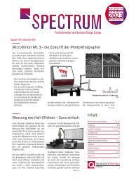
High frequencies in the DynaCool measurement system<br />
Apart from measurement options,<br />
our PPMS, DynaCool and VersaLab<br />
systems allow the integration of<br />
proprietary electronics or measurement<br />
setups. The Multifunction<br />
Probe (MFP) is a sample holder for<br />
measurements with proprietary cables,<br />
light guide and more which can<br />
easily be integrated in the cryostat<br />
and be connected with the sample.<br />
Just lately, we used the MFP in our<br />
application lab for a high-frequency<br />
measurement. The MFP was fitted<br />
with common RF cables. In a first<br />
test, we measured the frequency of<br />
a 4 MHz quartz crystal as function<br />
of temperature. We used a nanoVNA.<br />
Starting at 300 K (approx.<br />
3.9992 MHz),<br />
the quartz frequency<br />
decreases to about<br />
3.9946 MHz, at a<br />
temperature of 10 K.<br />
The figure shows the<br />
measurement data<br />
points S11 and the<br />
Vertical Standing<br />
Wave Ratio (VSWR) at<br />
300 K. The dip caused<br />
by the quartz oscillation<br />
is clearly visible.<br />
The MFP allows easy<br />
integration of hardware.<br />
Scripting enables<br />
measurement data of thirdparty<br />
devices to be integrated in<br />
the MultiVu software. Scripts, for<br />
example, may be integrated in the<br />
sequence.<br />
The PPMS, DynaCool and VersaLab<br />
are platforms for high magnetic<br />
fields and low temperatures which<br />
allow many automated measurement<br />
options for magnetic, thermal<br />
and electric sample characterization.<br />
Please contact us<br />
materials@qd-europe.com<br />
Lakeshore components inquiry portal<br />
Lakeshore offer a large number<br />
of temperature sensors, monitors<br />
and controllers. We have created a<br />
web portal to facilitate the selection<br />
of the right type of component.<br />
The web portal will automatically<br />
limit the possible options according<br />
to the specified requirements.<br />
Please follow this link:<br />
https://lakeshore.qd-europe.com<br />
to get an overview of all sensors,<br />
monitors and controllers.<br />
Please contact us<br />
cryo@qd-europe.com<br />
8
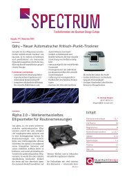
Cryogenics<br />
Cryogenic probe stations as turnkey measurement systems<br />
Lake Shore is the largest provider<br />
of cryogenic probe stations in the<br />
world. Probe stations allow efficient<br />
measurements on electronic components<br />
under controlled conditions.<br />
Temperature and magnetic field can<br />
be precisely adjusted. With only little<br />
effort, several samples can be measured<br />
in various ways through flexible<br />
probe tips. Sensors are available for<br />
DC-, HF and optical measurements.<br />
Additional technology like current<br />
source and voltmeter are normally<br />
supplied by the user. If the experimental<br />
setup requires central control,<br />
a corresponding script must<br />
be written to control the individual<br />
devices. This is particularly true for<br />
automized, temperature-dependent<br />
measurements.<br />
CRX-4K<br />
M81 – Synchronous Source Measure System<br />
Lake Shore now offers the first ready-to-use<br />
measurement modules as<br />
options for their probe stations, with<br />
proprietary MeasureLINK software<br />
used for control. Two modules are<br />
available so far:<br />
M81 – Synchronous Source<br />
Measure System<br />
M81 is a system made for electrical<br />
measurements. It enables AC and<br />
DC measurements for electric characterization.<br />
It features a modular<br />
setup and can be fitted with various<br />
sources and measuring units, depending<br />
on the measurement requirements.<br />
All modules are inherently<br />
synchronized.<br />
■ Electrical measurements with<br />
DC, AC, to 100 kHz and lock-in<br />
■ For special sensitivity requirements<br />
(nV, fA)<br />
■ Up to 3 source and 3 measure<br />
modules inherently synchronized<br />
M91 – FastHall<br />
M91 is configured for fast and precise<br />
Hall measurements. It provides a<br />
full Hall analysis incl. charge carrier<br />
mobility and concentration, Hall coefficient/voltage<br />
and magnetoresistance.<br />
Since the field polarity does<br />
not need to be switched during the<br />
measurement, even materials with<br />
low mobility can be measured in a<br />
short time.<br />
■ Automatic Hall analysis incl. van<br />
der Pauw and Hall bar geometry<br />
■ Large mobility range<br />
to 0.001 cm2/Vs<br />
■ Automatic optimization of excitation<br />
and measurement range<br />
■ High-resistance option to 200 GΩ<br />
Please contact us<br />
cryo@qd-europe.com<br />
Helium recovery with proprietary liquefaction<br />
We<br />
all<br />
We have a comprehensive guide<br />
on available helium recovery systems<br />
on our<br />
website [1]<br />
and would<br />
be happy to<br />
discuss your<br />
helium recovery<br />
requirements<br />
and<br />
options.<br />
provide<br />
necessary<br />
components. For example: Lab<br />
liquefiers with various capacities,<br />
NexGen helium liquefiers [2]<br />
and the coldhead-based helium<br />
gas purifier ATP-30 [3]. At the current<br />
helium prices, a liquefaction<br />
system pays off after only a few<br />
years.<br />
To get a first impression of the<br />
economic efficiency and the most<br />
profitable configuration, all we<br />
need is your yearly helium consumption.<br />
[1] https://qd-europe.comheliumintroduction/<br />
[2] https://qd-europe.com/heliumliquefier/<br />
[3] https://qd-europe.com/heliumgas-purifier/<br />
Please contact us<br />
cryo@qd-europe.com<br />
9 <strong>Spectrum</strong>, International edition 38| June 2022
Cryogenics/Imaging<br />
Recirculating cryocooler for "wet" cryostats<br />
Temperature (K)<br />
2.60<br />
2.55<br />
2.50<br />
2.45<br />
2.40<br />
2.35<br />
2.30<br />
2.25<br />
The recirculating cryocooler from<br />
Janis release “wet” cryostats from<br />
their dependency on liquid helium.<br />
Janis RGC4 series combines the advantages<br />
of cryo systems with open<br />
and closed cooling cycles.<br />
Instead of cooling the samples directly<br />
through the cold head of the<br />
cryocooler, a secondary cooling cycle<br />
is set up and the cold head of a<br />
Base temperature ST-500 microscopy cryostat<br />
cooled by the RGC4 system<br />
0 50 100 150 200 250<br />
Time (h)<br />
classic “wet” cryostat is cooled. This<br />
has several advantages:<br />
■ Same flexibility and convenience<br />
as a continuous-flow cryostat<br />
without liquid helium<br />
■ Quick sample change without<br />
warming up the RGC4 cooler<br />
■ Outstanding thermal performance<br />
■ Low vibration<br />
Pulse tube and GM<br />
coolers are available<br />
with 1 to 2W at<br />
4.2 K. The system<br />
also includes a<br />
gas handling system<br />
and dry scroll<br />
pump for gas circulation.<br />
Compatible<br />
cryostats are:<br />
■optical ST-100<br />
■non-optical ST-200<br />
■compact ST-300<br />
for use in a magnet<br />
■ UHV configuration ST-400 and<br />
■ microscopy configuration ST-500<br />
and the ST-500 based probe<br />
station<br />
Please contact us to discuss whether<br />
your cryostat from Janis or a third<br />
party provider is compatible with<br />
the recirculating cryocooler.<br />
Please contact us<br />
cryo@qd-europe.com<br />
New Xenics camera family – Ceres T<br />
Longwave microbolometer cameras<br />
measure temperatures in the ranges<br />
-20 to 120 °C and 50 to 400 °C. Thanks<br />
to the integrated FPGA, the Ceres T<br />
camera series is capable of quickly<br />
compensating any temperature variations.<br />
This means no more drifts<br />
in the results of longer-term measu-<br />
rements. The built-in electronics ensure<br />
precise measurements even of<br />
fast changing temperatures.<br />
The Ceres T camera family is available<br />
with either GigE with PoE or CameraLink<br />
interface. All cameras are<br />
GenICam compatible.<br />
The small-scale cameras<br />
are perfectly suited<br />
for both processing<br />
plant applications and<br />
lab experiments. The<br />
dimensions are 45 x<br />
45 x 67 mm<br />
3 and their<br />
weight starts from<br />
220 g.<br />
To ensure perfect temperature<br />
management,<br />
all lenses are firmly attached to the<br />
camera. Choose between the following<br />
horizontal FoVs: 12°, 16°, 25°<br />
and 48°.<br />
All cameras are available with either<br />
a 640 x 480 sensor or the new 1280 x<br />
1024 microbolometer.<br />
Please contact us<br />
imaging@qd-europe.com<br />
10
Materials science/Optics<br />
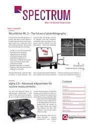
1.5 kW Laser-Based Floating Zone Furnace<br />
Quantum Design Japan have just<br />
launched a new version of their laser<br />
furnace for<br />
single crystal<br />
fabrication.<br />
In addition to the version with 2 kW<br />
laser power, there now is a version<br />
with 1.5 kW. It has 5 lasers with each<br />
300 W for homogeneous temperature<br />
distribution in the melting zone.<br />
The raw material blank is turned<br />
over a rotator and the melting zone<br />
is adjusted by moving the blank to<br />
create a single crystal. This process<br />
can lead to temperatures as high as<br />
2750 °C. The laser beam profile is optimized<br />
for crack-free single-crystal<br />
growth. The laser comes pre-aligned<br />
and does not need to be adjusted by<br />
the customer. Compared with IR furnaces<br />
with halogen or xenon lamps,<br />
a laser furnace impresses with its<br />
concentrated energy level in the<br />
melting zone, which makes it particularly<br />
suited for high-volatility materials.<br />
Please check out our website<br />
for images of single crystals grown<br />
with our laser furnaces. I look forward<br />
to discussing your application!<br />
https://qd-europe.com/laser-furnace/<br />
Please contact us<br />
materials@qd-europe.com<br />
MOXTEK Performance comparison tool<br />
Our partner MOXTEK boasts a wide<br />
range of polarizers and beamsplitters<br />
for a variety of applications.<br />
Their filters feature large acceptance<br />
angles of ±20° and high thermal<br />
stability to 200 °C (>5000 h). They are<br />
available as contrast or transmission<br />
optimized versions, reflecting or<br />
absorbing. To find the best solution<br />
among all these possibilities, Moxtek<br />
has developed a performance comparison<br />
tool. Compare typical parameters<br />
like Tp, Ts and Rp, Rs, contrast<br />
and efficiency at different AoIs. Further<br />
parameters are depicted in addition<br />
to the values in the specified<br />
areas for the selected filter types.<br />
https://compare.moxtek.com/<br />
By the way: Moxtek uses 200 mm<br />
wafers to produce polarizers and beamsplitters.<br />
Therefore all filters are<br />
available in sizes up to 180 mm in<br />
diameter and 130 mm x 130 mm in<br />
size.<br />
Please contact us<br />
optics@qd-europe.com<br />
Woollam-Newsletter – Edition 21 now released<br />
Woollam’s latest newsletter has been<br />
published! Edition 21 offers interesting<br />
features on spectroscopic ellipsometry<br />
and other topics around the<br />
Woollam company. One article deals<br />
with the options and performance of<br />
transmission Mueller matrix ellipsometry.<br />
Other topics are:<br />
■ An interview with Hans Arwin -<br />
his life dedicated to ellipsometry<br />
and his joy of reading<br />
■ Portrait of: Prof. Maurizio Canepa,<br />
University of Genoa<br />
In the article "Ellipsometry on flexible<br />
polarizing substrates", we present interesting<br />
case studies demonstrating<br />
the power of spectroscopic ellipsometry<br />
for flexible substrates and their devices.<br />
The entire article can be found in<br />
Woollam newsletter no. 21.<br />
Please contact us<br />
materials@qd-europe.com<br />
11 <strong>Spectrum</strong>, International edition 38| June 2022
Cryogenics/About us<br />
European Headquarters<br />
Quantum Design GmbH<br />
Im Tiefen See 58, 64293 Darmstadt, Germany<br />
Phone +49 6151 8806-0, Fax +49 6151 8806 920<br />
E-mail spectrum@qd-europe.com<br />
www.qd-europe.com<br />
Quantum Design BeNeLux<br />
Meerstraat 177<br />
B-1850 Grimbergen, Belgium<br />
Phone +32 2 3084324<br />
Mobile +32 495797175<br />
E-mail struyve@qd-europe.com<br />
Quantum Design Czech Rep. and Slovak. Rep.<br />
Krivoklatska 37, 199 00 Praha 9, Czech. Rep.<br />
Phone +420 607 014 278, Fax +420 24 1046850<br />
E-mail czechia@qd-europe.com<br />
Quantum Design France SARL<br />
Bâtiment Mac Kinley, 1, avenue de l’Atlantique,<br />
91940 Les Ulis, France<br />
Phone +33 1 69194949, Fax +33 1 69194930<br />
E-mail france@qd-europe.com<br />
Quantum Design Iberia<br />
(for Portugal and Spain)<br />
Roca i Roca, 45, 08226 Terrassa (Barcelona), Spain<br />
Phone and Fax +34 937349168<br />
E-mail boira@qd-europe.com<br />
Quantum Design s.r.l., Italia<br />
Via Francesco Sapori, 27<br />
00143 Roma, Italy<br />
Phone +39 06 5004204, Fax +39 06 5010389<br />
E-mail italy@qd-europe.com<br />
Quantum Design Magyarország<br />
Primet Méréstechnikai Kft<br />
Eszak u. 24, HU-1038 Budapest<br />
Phone and Fax +36 1 2402711,<br />
E-mail steinbach@qd-europe.com<br />
Quantum Design Nordic<br />
(for Denmark, Finland, Norway and Sweden)<br />
Roddarestigen 3, 182 35 Danderyd, Sweden<br />
Phone +46 8 41071791<br />
E-mail eriksson@qd-europe.com<br />
Quantum Design Przedstawicielstwo Polska<br />
Mikoów: tel.:+48 32 24457<br />
Fax: +48 32 4281169, kom.: +48 50 255112014<br />
pdluzewski@qd-europe.com lub<br />
Chorzów: tel.: +48 32 2482048<br />
Fax: +48 32 70 21 160, kom.: +48 51 5166893<br />
E-mail kowalczyk@qd-europe.com<br />
Quantum Design SRL<br />
(for Romania and Bulgaria)<br />
Str Ion Nistor Nr 4, et 1, M2E<br />
030041 Bucharest, Ro.<br />
Phone +40 75 50 39 900, Fax +40 31 7107156<br />
E-mail buiu@qd-europe.com<br />
Quantum Design AG Suisse<br />
Route du Roule 41, 1723 Marly, Switzerland<br />
Phone +41 21 8699033, Fax +41 21 8699308<br />
E-mail reinicke@qd-europe.com<br />
Electrical measurements at low temperatures<br />
– Multi-Contact Wedges<br />
The most common method to characterize<br />
electronic components at<br />
low temperatures are measurements<br />
through cryogenic probe stations.<br />
The systems combine up to six individually<br />
movable measuring tips<br />
with a cryostat. When more than 6<br />
contacts are required, you can use a<br />
Multi-Contact Wedge (MCW). An MCW<br />
is a wedge-shaped setup of a dozen or<br />
more measuring tips which are used<br />
instead of a single contact. A probe<br />
station can fit up to 6 MCWs. This facilitates<br />
more than enough contact<br />
points for any standard application.<br />
The setup is limited by the heat load<br />
because many feedthroughs lead to<br />
an increase in heat input. This can be<br />
May I introduce myself?<br />
My name is Merle Gerhardt. I finished<br />
my 2-year apprenticeship in<br />
wholesale and foreign trade with<br />
Quantum Design and am happy to<br />
be your commercial contact person<br />
in our cryotechnology and magnetism<br />
department.<br />
Before serving the apprenticeship, I<br />
had already worked as a volunteer in<br />
social work at the local Department<br />
of Children’s and Young People’s Affairs.<br />
avoided by choosing a probe station<br />
with a low base temperature.<br />
Lake Shore is the market leader for<br />
cryogenic probe stations. Multi-Contact<br />
Wedges can be used in all Lake<br />
Shore systems. GGB Industries, specialized<br />
in the manufacturing of<br />
measurements tips, provide customized<br />
MCWs.<br />
■ Temperature range: 2 K - 675 K<br />
■ Number of flexible probe pins: up to 6<br />
■ Magnetic field: up to 2.5 T<br />
been working<br />
as a voluntary<br />
organizer of<br />
youth camps.<br />
Please contact us<br />
cryo@qd-europe.com<br />
What I like most<br />
about working<br />
in the office are<br />
the versatile and<br />
interesting tasks that offer new challenges<br />
every day. I truly enjoy being<br />
part of the QD team and look forward<br />
to what the future has to offer.<br />
Quantum Design Turkey<br />
Phone: +90 544 741 99 97<br />
E-mail turkiye@qd-europe.com<br />
Quantum Design Ltd. UK and Ireland<br />
1 Mole Business Park, KT22 7BA Leatherhead,<br />
Surrey, United Kingdom<br />
Phone +44 13 72378822, Fax +44 13 72375353<br />
E-mail info@qd-uki.co.uk<br />
Quantum Design Russia<br />
(for Russia and Central Eurasia)<br />
Phone +7 495 938-1866 , Fax +7 495 938-1907<br />
E-mail academ@qd-europe.com<br />
When I am not working, you can find<br />
me outdoors. I love to work with<br />
plants and enjoy hiking and riding<br />
my bicycle. For six years, I have also<br />
Please contact us<br />
spectrum@qd-europe.com<br />
Follow us on LinkedIn:<br />
https://www.linkedin.com/<br />
company/quantum-design-europe<br />
Editor: Joachim Weiss, PhD<br />
Please note that not all products are available in every country.<br />
carbon neutral<br />
natureOffice.com | DE-617-226SY2T<br />
print production<br />
12