

DS1036 - Platform Manager Data Sheet - Lattice Semiconductor
DS1036 - Platform Manager Data Sheet - Lattice Semiconductor
DS1036 - Platform Manager Data Sheet - Lattice Semiconductor

Create successful ePaper yourself
Turn your PDF publications into a flip-book with our unique Google optimized e-Paper software.
February 2012 <strong>Data</strong> <strong>Sheet</strong> <strong>DS1036</strong><br />
Features<br />
� Precision Voltage Monitoring Increases�<br />
Reliability<br />
• 12 independent analog monitor inputs<br />
Differential inputs for remote ground sense<br />
Two programmable threshold comparators per<br />
analog input<br />
Hardware window comparison<br />
10-bit ADC for I 2 C monitoring<br />
� High-Voltage FET Drivers Enable<br />
Integration<br />
Power supply ramp up/down control<br />
Programmable current and voltage output<br />
Independently configurable for FET control or<br />
digital output<br />
� Power Supply Margin and Trim Functions<br />
Trim and margin up to eight power supplies<br />
Dynamic voltage control through I 2 C<br />
Independent Digital Closed-Loop Trim function<br />
for each output<br />
� Programmable Timers Increase Control<br />
Flexibility<br />
Four independent timers<br />
32 �s to 2 second intervals for timing sequences<br />
� PLD Resources Integrate Power and Digital<br />
Functions<br />
48-macrocell CPLD<br />
640 LUT4s FPGA<br />
Up to 107 digital I/Os<br />
Up to 6.1 Kbits distributed RAM<br />
� Programmable sysIO Buffer Supports a<br />
Range of Interfaces<br />
LVCMOS 3.3/2.5/1.8/1.5/1.2<br />
LVTTL<br />
� System-Level Support<br />
Single 3.3V supply operation<br />
Industrial temperature range: -40°C to +85°C<br />
� In-System Programmability Reduces Risk<br />
Integrated non-volatile configuration memory<br />
JTAG programming interface<br />
� Package Options<br />
128-pin TQFP<br />
208-ball ftBGA<br />
RoHS compliant and halogen-free<br />
<strong>Platform</strong> <strong>Manager</strong><br />
In-System Programmable Power and Digital<br />
Board Management<br />
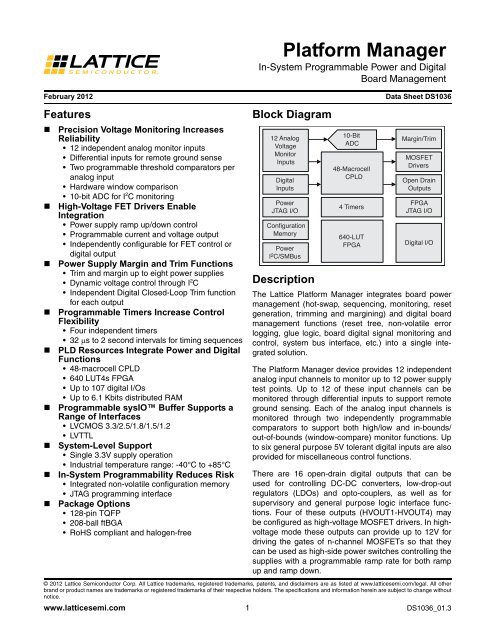
Block Diagram<br />
12 Analog<br />
Voltage<br />
Monitor<br />
Inputs<br />
Digital<br />
Inputs<br />
Power<br />
JTAG I/O<br />
Configuration<br />
Memory<br />
Power<br />
II 2C/SMBus<br />
Description<br />
Margin/Trim<br />
MOSFET<br />
Drivers<br />
Open Drain<br />
Outputs<br />
Digital I/O<br />
© 2012 <strong>Lattice</strong> <strong>Semiconductor</strong> Corp. All <strong>Lattice</strong> trademarks, registered trademarks, patents, and disclaimers are as listed at www.latticesemi.com/legal. All other<br />
brand or product names are trademarks or registered trademarks of their respective holders. The specifications and information herein are subject to change without<br />
notice.<br />
www.latticesemi.com 1 <strong>DS1036</strong>_01.3<br />
10-Bit<br />
ADC<br />
48-Macrocell<br />
CPLD<br />
4 Timers<br />
640-LUT<br />
FPGA<br />
FPGA<br />
JTAG I/O<br />
The <strong>Lattice</strong> <strong>Platform</strong> <strong>Manager</strong> integrates board power<br />
management (hot-swap, sequencing, monitoring, reset<br />
generation, trimming and margining) and digital board<br />
management functions (reset tree, non-volatile error<br />
logging, glue logic, board digital signal monitoring and<br />
control, system bus interface, etc.) into a single integrated<br />
solution.<br />
The <strong>Platform</strong> <strong>Manager</strong> device provides 12 independent<br />
analog input channels to monitor up to 12 power supply<br />
test points. Up to 12 of these input channels can be<br />
monitored through differential inputs to support remote<br />
ground sensing. Each of the analog input channels is<br />
monitored through two independently programmable<br />
comparators to support both high/low and in-bounds/<br />
out-of-bounds (window-compare) monitor functions. Up<br />
to six general purpose 5V tolerant digital inputs are also<br />
provided for miscellaneous control functions.<br />
There are 16 open-drain digital outputs that can be<br />
used for controlling DC-DC converters, low-drop-out<br />
regulators (LDOs) and opto-couplers, as well as for<br />
supervisory and general purpose logic interface functions.<br />
Four of these outputs (HVOUT1-HVOUT4) may<br />
be configured as high-voltage MOSFET drivers. In highvoltage<br />
mode these outputs can provide up to 12V for<br />
driving the gates of n-channel MOSFETs so that they<br />
can be used as high-side power switches controlling the<br />
supplies with a programmable ramp rate for both ramp<br />
up and ramp down.
2<br />
<strong>Platform</strong> <strong>Manager</strong> <strong>Data</strong> <strong>Sheet</strong><br />
The board power management function can be implemented using an internal 48-macrocell CPLD. The status of all<br />
of the comparators on the analog input channels as well as the general purpose digital inputs are used as inputs by<br />
the CPLD array, and all digital outputs (open-drain as well as HVOUT) may be controlled by the CPLD.<br />
Four independently programmable timers can create delays and time-outs ranging from 32 �s to 2 seconds.<br />
The <strong>Platform</strong> <strong>Manager</strong> device incorporates up to eight DACs for generating trimming voltage to control the output<br />
voltage of a DC-DC converter. Additionally, each power supply output voltage can be maintained typically within<br />
0.5% tolerance across various load conditions using the Digital Closed Loop Control mode.<br />
The internal 10-bit A/D converter can both be used to monitor the VMON voltage through the I 2 C bus as well as for<br />
implementing digital closed loop mode for maintaining the output voltage of all power supplies controlled by the<br />
monitoring and trimming section of the <strong>Platform</strong> <strong>Manager</strong> device.<br />
The FPGA section of the <strong>Platform</strong> <strong>Manager</strong> is optimized to meet the requirements of board management functions<br />
including reset distribution, boundary scan management, fault logging, FPGA load control, and system bus interface.<br />
The FPGA section uses look-up tables (LUTs) and distributed memories for flexible and efficient logic implementation.<br />
This instant-on capability enables the <strong>Platform</strong> <strong>Manager</strong> devices to integrate control functions that are<br />
required as soon as power is applied to the board.<br />
Power management functions can be integrated into the CPLD and digital board management functions can be<br />
integrated into the FPGA using the LogiBuilder tool provided by PAC-Designer ® software. In addition, the FPGA<br />
designs can also be implemented in VHDL or Verilog HDL through the ispLEVER ® software design tool.<br />
The <strong>Platform</strong> <strong>Manager</strong> IC supports a hardware I 2 C/SMBus slave interface that can be used to measure voltages<br />
through the Analog to Digital Converter or is used for trimming and margining using a microcontroller.<br />
There are two JTAG ports integrated into the <strong>Platform</strong> <strong>Manager</strong> device: Power JTAG and FPGA JTAG. The Power<br />
JTAG interface is used to program the power section of the <strong>Platform</strong> <strong>Manager</strong> and the FPGA JTAG is used to configure<br />
the FPGA portion of the device. The FPGA configuration memory can be changed in-system without interrupting<br />
the operation of the board management section. However, the Power Management section of the platform<br />
<strong>Manager</strong> cannot be changed without interrupting the power management operation.<br />
Table 1. <strong>Platform</strong> <strong>Manager</strong> Family Selection Table<br />
Parameter LPTM10-1247 LPTM10-12107<br />
Analog Inputs 12 12<br />
Margin and Trim 6 8<br />
Total I/O 47 107<br />
CPLD Macrocells 48 48<br />
FPGA LUTs 640 640<br />
Package 128-pin TQFP 208-ball ftBGA
Figure 1. Typical <strong>Platform</strong> <strong>Manager</strong> Application<br />
SPI Memory<br />
12V Backplane Vin<br />
VID<br />
4<br />
I 2 C Interface<br />
CPU_ Reset<br />
4<br />
SPI<br />
Port<br />
12V<br />
Current<br />
Monitor<br />
<strong>Platform</strong> <strong>Manager</strong><br />
Processor<br />
Interface<br />
3<br />
Hot-Swap<br />
FET Control<br />
Margin & Trim<br />
<strong>Platform</strong> <strong>Manager</strong> <strong>Data</strong> <strong>Sheet</strong><br />
Note: See reference design, IP documentation and application notes for more information on implementation of<br />
individual functions called out above.<br />
3.3V<br />
1.2V<br />
1.0V<br />
Supply Sequencing<br />
Voltage Monitoring<br />
Reset Distribution
1, 2, 3<br />
Absolute Maximum Ratings<br />
4<br />
<strong>Platform</strong> <strong>Manager</strong> <strong>Data</strong> <strong>Sheet</strong><br />
Power Management Core Supply PVCCD . . . . . . . . . . . . . . . . . . . . . . . . . . . . . . . . . . .-0.5 to 4.5V<br />
Power Management Analog Supply PVCCA . . . . . . . . . . . . . . . . . . . . . . . . . . . . . . . . .-0.5 to 4.5V<br />
Power Management Digital Input Supply PVCCA (IN[1:4]) PVCCINP . . . . . . . . . . . . . . . -0.5 to 6V<br />
Power Management JTAG Logic Supply PVCCJ . . . . . . . . . . . . . . . . . . . . . . . . . . . . . -0.5 to 6V<br />
Power Management Alternate E2 programming supply APS4 . . . . . . . . . . . . . . . . . . . -0.5 to 4V<br />
Power Management Digital Input Voltage (All Digital I/O Pins) VIN . . . . . . . . . . . . . . . -0.5 to 6V<br />
VMON Input Voltage . . . . . . . . . . . . . . . . . . . . . . . . . . . . . . . . . . . . . . . . . . . . . . . . . . -0.5 to 6V<br />
VMON Input Voltage Ground Sense . . . . . . . . . . . . . . . . . . . . . . . . . . . . . . . . . . . . . . -0.5 to 6V<br />
Voltage Applied to Power Management Tri-stated Pins (HVOUT[1:4]) . . . . . . . . . . . -0.5 to 13.3V<br />
Voltage Applied to Power Management Tri-stated Pins (OUT[5:16]). . . . . . . . . . . . . . -0.5 to 6V<br />
Maximum Sink Current on Any Power Management Output . . . . . . . . . . . . . . . . . . . . . .23 mA<br />
FPGA Supply Voltage VCC . . . . . . . . . . . . . . . . . . . . . . . . . . . . . . . . . . . . . . . . . . . . -0.5 to 3.75V<br />
FPGA Supply Voltage VCCAUX . . . . . . . . . . . . . . . . . . . . . . . . . . . . . . . . . . . . . . . . . -0.5 to 3.75V<br />
FPGA Output Supply Voltage VCCIO . . . . . . . . . . . . . . . . . . . . . . . . . . . . . . . . . . . . -0.5 to 3.75V<br />
FPGA I/O Tri-state Voltage Applied5 . . . . . . . . . . . . . . . . . . . . . . . . . . . . . . . . . . . . . -0.5 to 3.75V<br />
FPGA Dedicated Input Voltage Applied5 . . . . . . . . . . . . . . . . . . . . . . . . . . . . . . . . . . -0.5 to 4.25V<br />
Device Storage Temperature . . . . . . . . . . . . . . . . . . . . . . . . . . . . . . . . . . . . . . . . . . .-65 to +150°C<br />
Junction Temperature TJ . . . . . . . . . . . . . . . . . . . . . . . . . . . . . . . . . . . . . . . . . . . . . . . +125°C<br />
1. Stress above those listed under the “Absolute Maximum Ratings” may cause permanent damage to the device. Functional operation of the<br />
device at these or any other conditions above those indicated in the operational sections of this specification is not implied.<br />
2. Compliance with the <strong>Lattice</strong> Thermal Management document is required.<br />
3. All voltages referenced to GND (FPGA section) or GNDA/D (Power sections).<br />
4. The APS pin MUST be left floating when PVCCD and PVCCA are powered.<br />
5. Overshoot and undershoot of -2V to (V IHMAX + 2) volts is permitted for a duration of
Recommended Operating Conditions<br />
1, 2, 3<br />
Digital I/O Hot Socketing Specifications<br />
5<br />
<strong>Platform</strong> <strong>Manager</strong> <strong>Data</strong> <strong>Sheet</strong><br />
Symbol Parameter Conditions Min. Max. Units<br />
1 PVCCD, PVCCA Core supply voltage at pin 2.8 3.96 V<br />
PVCCINP Digital input supply for IN[1:4] at pin 2.25 5.5 V<br />
PVCCJ JTAG logic supply voltage at pin 2.25 3.6 V<br />
APS Alternate E2 programming supply at pin PVCCD and PVCCA powered<br />
No Connect<br />
Must Be Left Floating<br />
PVCCD and PVCCA not powered 3.0 3.6 V<br />
VIN Input voltage at digital input pins -0.3 5.5 V<br />
VMON Input voltage at VMON pins -0.3 5.9 V<br />
VMONGS Input voltage at VMONGS pins -0.2 0.3 V<br />
V OUT<br />
2<br />
VCC 2<br />
VCCAUX V CCIO 3<br />
t JCOM<br />
t JIND<br />
t JFLASHCOM<br />
t JFLASHIND<br />
OUT[5:16] pins -0.3 5.5 V<br />
Open-drain output voltage<br />
HVOUT[1:4] pins in open-drain<br />
mode<br />
-0.3 13.0 V<br />
FPGA Core Supply Voltage 3.135 3.465 V<br />
FPGA Auxiliary Supply Voltage 3.135 3.465 V<br />
FPGA I/O Driver Supply Voltage<br />
Junction Temperature Commercial<br />
Operation<br />
Junction Temperature Industrial<br />
Operation<br />
Junction Temperature, Flash<br />
Programming, Commercial<br />
Junction Temperature, Flash<br />
Programming, Industrial<br />
VCCIO0, VCCIO1, VCCIO3 1.14 3.465 V<br />
VCCIO2 2.25 3.6 V<br />
Power applied 0 +85<br />
Power applied -40 +100<br />
0 +85<br />
-40 +100<br />
1. P VCCD and P VCCA must always be tied together.<br />
2. V CC and V CCAUX must always be tied together. Also, like power supplies must be tied together. For example, if V CCIO and V CC are both<br />
3.3V, they must also be the same supply.<br />
3. See recommended voltages by I/O standard in subsequent table.<br />
Symbol Parameter Condition Min. Typ. Max Units<br />
IDK Input or I/O leakage Current 0 � VIN � VIH (MAX) — — +/-1000 µA<br />
1. Assumes monotonic rise/fall rates for VCC, VCCAUX, and VCCIO. 2. 0 � VCC � VCC (MAX), 0 � VCCIO � VCCIO (MAX) and 0 � VCCAUX � VCCAUX (MAX).<br />
3.IDK is additive to IPU, IPD or IBH. o C<br />
o C<br />
o C<br />
o C
Power-On Reset – Power Management Section<br />
Figure 2. Power Management Section Power-On Reset<br />
6<br />
<strong>Platform</strong> <strong>Manager</strong> <strong>Data</strong> <strong>Sheet</strong><br />
Symbol Parameter Conditions Min. Typ. Max. Units<br />
TRST Delay from VTH to start-up state 100 µs<br />
TSTART Delay from RESETb HIGH to CPLDCLK<br />
rising edge<br />
5 10 µs<br />
TGOOD Power-on reset to valid VMON comparator<br />
output and AGOOD is true<br />
2.5 ms<br />
TBRO Minimum duration brown out required to<br />
trigger RESETb<br />
1 5 µs<br />
TPOR Delay from brown out to reset state. 13 µs<br />
VTL Threshold below which RESETb is LOW 1<br />
2.3 V<br />
VTH Threshold above which RESETb is HIGH 1<br />
2.7 V<br />
VT Threshold above which RESETb is valid 1<br />
0.8 V<br />
CL Capacitive load on RESETb for master/slave<br />
operation<br />
200 pF<br />
1. Corresponds to PVCCA and PVCCD supply voltages.<br />
V TH<br />
V TL<br />
V T<br />
Reset<br />
State<br />
T RST<br />
T START<br />
Start Up<br />
State<br />
Analog Calibration<br />
T GOOD<br />
T BRO<br />
T POR<br />
PVCCD, PVCCA<br />
RESETb<br />
MCLK<br />
CPLDCLK<br />
AGOOD (Internal)
ESD Performance<br />
All pins<br />
Pin Group ESD Stress Min. Units<br />
1, 2, 3, 4<br />
DC Electrical Characteristics<br />
1, 2<br />
FPGA Supply Current (Sleep Mode)<br />
HBM 1500 V<br />
CDM 1000 V<br />
7<br />
<strong>Platform</strong> <strong>Manager</strong> <strong>Data</strong> <strong>Sheet</strong><br />
Symbol Parameter Conditions Typ. 5<br />
Max. Units<br />
PICC Power Management section supply current Normal operation 40 mA<br />
PICCINP Power Management section supply current Normal operation 5 mA<br />
PICCJ Power Management section supply current Normal operation 1 mA<br />
1 ICC FPGA Core Power Supply 8.7 mA<br />
ICCAUX FPGA Auxiliary Power Supply<br />
VCCAUX = 3.3V<br />
During initialization (0MHz) 7 mA<br />
ICCIO FPGA Bank Power Supply 6<br />
During initialization (0MHz) 2.4 mA<br />
1. For further information on FPGA section supply current, please see details of additional technical documentation at the end of this data<br />
sheet.<br />
2. Assumes all FPGA section I/O pins are held at VCCIO or GND.<br />
3. FPGA Frequency = 0 MHz.<br />
4. Typical FPGA user pattern.<br />
5. TJ = 25oC, power supplies at nominal voltage.<br />
6. Per bank, VCCIO = 2.5V. Does not include pull-up/pull-down.<br />
Symbol Parameter Conditions Typ. 3<br />
Max. Units<br />
1 ICC FPGA Core Power Supply Sleep Mode 12 25 µA<br />
ICCAUX FPGA Auxiliary Power Supply 1 25 µA<br />
ICCIO Bank Power Supply 4<br />
2 30 µA<br />
1. Assumes all inputs are configured as LVCMOS and held at the VCCIO or GND.<br />
2. Frequency = 0MHz.<br />
3. TA = 25°C, power supplies at nominal voltage.<br />
4. Per bank.
DC Electrical Characteristics – FPGA General Purpose I/O<br />
Over Recommended Operating Conditions<br />
8<br />
<strong>Platform</strong> <strong>Manager</strong> <strong>Data</strong> <strong>Sheet</strong><br />
Symbol Parameter Condition Min. Typ. Max. Units<br />
1, 4 IIL, IIH Input or I/O Leakage<br />
0 � VIN � (VCCIO - 0.2V)<br />
(VCCIO - 0.2V) < VIN � 3.6V<br />
—<br />
—<br />
—<br />
—<br />
10<br />
40<br />
µA<br />
µA<br />
IPU I/O Active Pull-up Current 0 � VIN � 0.7 VCCIO -30 — -150 µA<br />
IPD I/O Active Pull-down Current VIL (MAX) � VIN � VIH (MAX) 30 — 150 µA<br />
IBHLS Bus Hold Low sustaining current VIN = VIL (MAX) 30 — — µA<br />
IBHHS Bus Hold High sustaining current VIN = 0.7VCCIO -30 — — µA<br />
IBHLO Bus Hold Low Overdrive current 0 � VIN � VIH (MAX) — — 150 µA<br />
IBHHO Bus Hold High Overdrive current 0 � VIN � VIH (MAX) — — -150 µA<br />
3 VBHT Bus Hold trip Points 0 � VIN � VIH (MAX) VIL (MAX) — VIH (MIN) V<br />
C1 I/O Capacitance2 VCCIO = 3.3V, 2.5V, 1.8V, 1.5V, 1.2V,<br />
VCC = Typ., VIO = 0 to VIH (MAX)<br />
— 8 — pf<br />
C2 Dedicated Input Capacitance 2 VCCIO = 3.3V, 2.5V, 1.8V, 1.5V, 1.2V,<br />
VCC = Typ., VIO = 0 to VIH (MAX)<br />
— 8 — pf<br />
1. Input or I/O leakage current is measured with the pin configured as an input or as an I/O with the output driver tri-stated. It is not measured<br />
with the output driver active. Bus maintenance circuits are disabled.<br />
2. TA 25°C, f = 1.0MHz<br />
3. Please refer to VIL and VIH in the sysIO Single-Ended DC Electrical Characteristics table of this document.<br />
4. When VIH is higher than VCCIO, a transient current typically of 30ns in duration or less with a peak current of 6mA can occur on the high-tolow<br />
transition.
1, 2, 3, 4<br />
Programming and Erase Supply Current<br />
Voltage Monitors<br />
Single-Ended Voltage Monitor Trip Point Error 1<br />
9<br />
<strong>Platform</strong> <strong>Manager</strong> <strong>Data</strong> <strong>Sheet</strong><br />
Symbol Parameter Typ. 5<br />
Max. Units<br />
IAPS Power Management PVCCA/D Programming Current<br />
40 mA<br />
ICC FPGA Core Power Supply 11 mA<br />
ICCAUX FPGA Auxiliary Power Supply<br />
VCCAUX = 3.3V<br />
10 mA<br />
ICCIO FPGA Bank Power Supply 6<br />
2 mA<br />
1. For further information on supply current, please see details of additional technical documentation at the end of this data sheet.<br />
2. Assumes all I/O pins are held at VCCIO or GND.<br />
3. Typical user pattern.<br />
4. JTAG programming is at 25 MHz.<br />
5. TJ = 25°C, power supplies at nominal voltage.<br />
6. Per bank. VCCIO = 2.5V. Does not include pull-up/pull-down.<br />
Symbol Parameter Conditions Min. Typ. Max. Units<br />
RIN Input resistance 55 65 75 k�<br />
CIN Input capacitance 8 pF<br />
VMON Range Programmable trip-point range 0.075 5.734 V<br />
VZ Sense Near-ground sense threshold 70 75 80 mV<br />
V MON Accuracy<br />
Absolute accuracy of any trip-point 1<br />
2, 3<br />
Single-ended VMON pins<br />
0.2 0.7 %<br />
0.3 0.9 %<br />
HYST<br />
Hysteresis of any trip-point<br />
(relative to setting)<br />
1 %<br />
CMR Common mode rejection 60 dB<br />
tPD16 Propagation delay input to output<br />
glitch filter OFF<br />
16 µs<br />
tPD64 Propagation delay input to output<br />
glitch filter ON<br />
64 µs<br />
1. Guaranteed by characterization across P VCCA range, operating temperature, process.<br />
2. Single-ended V MON inputs in 128-pin TQFP package only. Single-ended V MON input pins include: 59 (V MON1 ), 83 (V MON9 ), 84 (V MON10 ), 86<br />
(V MON11), 88 (V MON12).<br />
3. No adjacent digital I/O pin switching noise as described in the following table for single-ended V MON trip point error.<br />
Symbol Parameter Conditions Min. Typ. Max. Units<br />
V MON Error SE<br />
Single-ended trip point error<br />
(with adjacent switching noise) 2<br />
Single-ended trip point error<br />
(no adjacent switching noise) 2<br />
Pins 85, 87, 89<br />
FSWITCH = 10MHz<br />
Pins 85, 87, 89<br />
FSWITCH = 0Hz;<br />
All other digital I/O = 10MHz<br />
2 mV<br />
1 mV<br />
1. Single-ended V MON inputs in 128-pin TQFP package only. Affected single-ended V MON input pins only include: 83 (V MON9), 84 (V MON10),<br />
86 (V MON11 ), and 88 (V MON12 ). Single-ended Vmon input pin 59 (V MON1 ) is not affected by adjacent switching noise.<br />
2. Defined as TQFP package option adjacent digital I/O pins 85 (PR4B), 87 (PR3D) and 89 (PR2D) configured as outputs switching (F SWITCH)<br />
at 10MHz into a 33pF load capacitance.
High Voltage FET Drivers<br />
V PP<br />
Margin/Trim DAC Output Characteristics<br />
10<br />
<strong>Platform</strong> <strong>Manager</strong> <strong>Data</strong> <strong>Sheet</strong><br />
Symbol Parameter Conditions Min. Typ. Max. Units<br />
I OUTSRC<br />
I OUTSINK<br />
Gate driver output voltage<br />
Gate driver source current �<br />
(HIGH state)<br />
Gate driver sink current �<br />
(LOW state)<br />
12V setting 11.5 12 12.5<br />
10V setting 9.6 10 10.4<br />
8V setting 7.7 8 8.3<br />
6V setting 5.8 6 6.2<br />
Four settings in �<br />
software<br />
12.5<br />
25<br />
50<br />
100<br />
FAST OFF mode 2000 3000<br />
Controlled ramp �<br />
settings<br />
Symbol Parameter Conditions Min. Typ. Max. Units<br />
Resolution 8 (7+sign) Bits<br />
FSR Full scale range +/-320 mV<br />
LSB LSB step size 2.5 mV<br />
IOUT Output source/sink current -200 200 µA<br />
Offset 1 0.6<br />
BPZ<br />
Bipolar zero output voltage<br />
(code=80h)<br />
Offset 2<br />
Offset 3<br />
0.8<br />
1.0<br />
V<br />
Offset 4 1.25<br />
TS<br />
TrimCell output voltage settling<br />
time 1<br />
DAC code changed<br />
from 80H to FFH or<br />
80H to 00H<br />
Single DAC code<br />
change<br />
256<br />
2.5 ms<br />
µs<br />
C_LOAD Maximum load capacitance 50 pF<br />
TUPDATEM Update time through I 2 C port 2<br />
MCLK = 8 MHz 260 µs<br />
TOSE<br />
Total open loop supply voltage<br />
error 3<br />
Full scale DAC corresponds<br />
to ±5% supply<br />
voltage variation<br />
-1% +1% V/V<br />
1. To 1% of set value with 50pf load connected to trim pins.<br />
2. Total time required to update a single TRIMx output value by setting the associated DAC through the I2C port.<br />
3. This is the total resultant error in the trimmed power supply output voltage referred to any DAC code due to the DAC’s INL, DNL, gain, output<br />
impedance, offset error and bipolar offset error across the industrial temperature range and the <strong>Platform</strong> <strong>Manager</strong> operating PVCCA and<br />
PVCCD ranges.<br />
100<br />
250<br />
500<br />
V<br />
µA<br />
µA
ADC Characteristics<br />
ADC Error Budget Across Entire Operating Temperature Range<br />
11<br />
<strong>Platform</strong> <strong>Manager</strong> <strong>Data</strong> <strong>Sheet</strong><br />
Symbol Parameter Conditions Min. Typ. Max. Units<br />
ADC Resolution 10 Bits<br />
TCONVERT Conversion Time Time from I 2 C Request 200 µs<br />
V IN<br />
Input range Full Scale<br />
Programmable Attenuator = 1 0 2.048 V<br />
Programmable Attenuator = 3 0 5.9 1<br />
V<br />
ADC Step Size LSB<br />
Programmable Attenuator = 1<br />
Programmable Attenuator = 3<br />
2<br />
6<br />
mV<br />
mV<br />
Eattenuator Error Due to Attenuator Programmable Attenuator = 3 +/- 0.1 %<br />
1. Maximum voltage is limited by VMONX pin (theoretical maximum is 6.144V).<br />
Symbol Parameter Conditions Min. Typ. Max. Units<br />
TADC Error<br />
Total Measurement Error at<br />
Any Voltage (Differential Analog<br />
Inputs) 1<br />
Total Measurement Error at<br />
Any Voltage (Single-Ended<br />
Analog Inputs) 2<br />
Measurement Range 600 mV - 2.048V,<br />
VMONxGS > -100mV, Attenuator =1<br />
Measurement Range 600 mV - 2.048V,<br />
VMONxGS > -200mV, Attenuator =1<br />
Measurement Range 0 - 2.048V,<br />
VMONxGS > -200mV, Attenuator =1<br />
Measurement Range 600 mV - 2.048V,<br />
Attenuator =1<br />
-8 +/-4 8 mV<br />
+/-6 mV<br />
+/-10 mV<br />
-8 +/-4 8 mV<br />
1. Total error, guaranteed by characterization, includes INL, DNL, Gain, Offset, and PSR specifications of the ADC.<br />
2. Single-ended V MON inputs in 128-pin TQFP package only. Single-ended Vmon input pins include: 59 (VMON1), 83 (VMON9), 84<br />
(VMON10), 86 (VMON11), 88 (VMON12).
12<br />
<strong>Platform</strong> <strong>Manager</strong> <strong>Data</strong> <strong>Sheet</strong><br />
Digital Specifications – Power Management Section Dedicated Inputs<br />
Over Recommended Operating Conditions<br />
Symbol Parameter Conditions Min. Typ. Max. Units<br />
IIL ,IIH Input leakage, no pull-up/pull-down +/-10 µA<br />
IPU Input pull-up current (PTMS, PTDI,<br />
PTDISEL, PATDI, MCLK)<br />
70 µA<br />
V IL<br />
Voltage input, logic low 1<br />
PTDI, PTMS, PATDI,<br />
PTDISEL, 3.3V supply<br />
PTDI, PTMS, PATDI,<br />
PTDISEL, 2.5V supply<br />
0.7<br />
SCL, SDA 30% PVCCD IN[1:4] 30% PVCCINP PTDI, PTMS, PATDI,<br />
PTDISEL, 3.3V supply<br />
2.0<br />
VIH Voltage input, logic high 1<br />
PTDI,P TMS, PATDI,<br />
PTDISEL, 2.5V supply<br />
1.7<br />
SCL, SDA 70% PVCCD PVCCD IN[1:4] 70% PVCCINP PVCCINP 1. SCL, SDA referenced to PVCCD; IN[1:4] referenced to PVCCINP; PTDO, PTDI, PTMS, PATDI, PTDISEL referenced to PVCCJ. Digital Specifications – Power Management Section Dedicated Outputs<br />
Over Recommended Operating Conditions<br />
Symbol Parameter Conditions Min. Typ. Max. Units<br />
IOH-HVOUT Output leakage current<br />
HVOUT[1:4] in open<br />
drain mode and pulled<br />
up to 12V<br />
35 100 µA<br />
VOL HVOUT[1:4] (open drain mode), ISINK = 10mA 0.8 V<br />
OUT[5:16] ISINK = 20mA 0.8<br />
PTDO, MCLK, CPLDCLK, SDA ISINK = 4mA 0.4<br />
VOH PTDO, MCLK, CPLDCLK ISRC = 4mA PVCCD - 0.4 V<br />
ISINKTOTAL All digital outputs 130 mA<br />
0.8<br />
V<br />
V
sysIO Recommended Operating Conditions<br />
Standard<br />
Min. Typ. Max.<br />
LVCMOS 3.3 3.135 3.3 3.465<br />
LVCMOS 2.5 2.375 2.5 2.625<br />
LVCMOS 1.8 1.71 1.8 1.89<br />
LVCMOS 1.5 1.425 1.5 1.575<br />
LVCMOS 1.2 1.14 1.2 1.26<br />
LVTTL 3.135 3.3 3.465<br />
sysIO Single-Ended DC Electrical Characteristics<br />
Input/Output<br />
Standard<br />
13<br />
V CCIO (V)<br />
VIL VIH VOL Max.<br />
Min. (V) Max. (V) Min. (V) Max. (V) (V)<br />
LVCMOS 3.3 -0.3 0.8 2.0 3.6<br />
LVTTL -0.3 0.8 2.0 3.6<br />
LVCMOS 2.5 -0.3 0.7 1.7 3.6<br />
LVCMOS 1.8 2<br />
LVCMOS 1.5 2<br />
-0.3 0.35V CCIO 0.65V CCIO 3.6<br />
-0.3 0.35V CCIO 0.65V CCIO 3.6<br />
<strong>Platform</strong> <strong>Manager</strong> <strong>Data</strong> <strong>Sheet</strong><br />
V OH Min.<br />
(V)<br />
I OL 1<br />
(mA)<br />
I OH 1<br />
(mA)<br />
0.4 VCCIO - 0.4 16, 12, 8, 4 -14, -12, -8, -4<br />
0.2 VCCIO - 0.2 0.1 -0.1<br />
0.4 2.4 16 -16<br />
0.4 VCCIO - 0.4 12, 8, 4 -12, -8, -4<br />
0.2 VCCIO - 0.2 0.1 -0.1<br />
0.4 VCCIO - 0.4 16, 12, 8, 4 -14, -12, -8, -4<br />
0.2 VCCIO - 0.2 0.1 -0.1<br />
0.4 VCCIO - 0.4 16, 12, 8, 4 -14, -12, -8, -4<br />
0.2 VCCIO - 0.2 0.1 -0.1<br />
0.4 VCCIO - 0.4 8, 4 -8, -4<br />
0.2 VCCIO - 0.2 0.1 -0.1<br />
LVCMOS 1.2 2<br />
0.4 VCCIO - 0.4 6, 2 -6, -2<br />
-0.3 0.42 0.78 3.6<br />
0.2 VCCIO - 0.2 0.1 -0.1<br />
1. The average DC current drawn by I/Os between GND connections, or between the last GND in an I/O bank and the end of an I/O bank, as<br />
shown in the logic signal connections table shall not exceed n * 8mA. Where n is the number of I/Os between bank GND connections or<br />
between the last GND in a bank and the end of a bank.<br />
2. Lower voltage operation not supported for VCCIO2 bank pins.
sysIO Differential Electrical Characteristics<br />
LVDS Emulation<br />
14<br />
<strong>Platform</strong> <strong>Manager</strong> <strong>Data</strong> <strong>Sheet</strong><br />
FPGA section outputs can support LVDS outputs via emulation (LVDS25E), in addition to the LVDS support that is<br />
available. The output is emulated using complementary LVCMOS outputs in conjunction with resistors across the<br />
driver outputs on all devices. The scheme shown in Figure 3 is one possible solution for LVDS standard implementation.<br />
Resistor values in Figure 3 are industry standard values for 1% resistors.<br />
Figure 3. LVDS Using External Resistors (LVDS25E)<br />
BLVDS Emulation<br />
FPGA outputs support the BLVDS standard through emulation. The output is emulated using complementary LVC-<br />
MOS outputs in conjunction with a parallel external resistor across the driver outputs. BLVDS is intended for use<br />
when multi-drop and bi-directional multi-point differential signaling is required. The scheme shown in Figure 4 is<br />
one possible solution for bi-directional multi-point differential signals.<br />
Figure 4. BLVDS Multi-point Output Example<br />
2.5V<br />
16mA<br />
16mA<br />
2.5V<br />
+<br />
-<br />
LVPECL Emulation<br />
VCCIO = 2.5<br />
8mA<br />
VCCIO = 2.5<br />
8mA<br />
158<br />
158<br />
140<br />
Zo = 100<br />
Internal<br />
Emulated<br />
LVDS<br />
Buffer<br />
External External Internal<br />
Note: All resistors are ±1%.<br />
Heavily loaded backplane, effective Zo ~ 45 to 90 ohms differential<br />
80<br />
80<br />
45-90 ohms 45-90 ohms<br />
80<br />
80<br />
2.5V 2.5V<br />
-<br />
2.5V 2.5V<br />
16mA 16mA 16mA 16mA<br />
+<br />
FPGA outputs support the differential LVPECL standard through emulation. This output standard is emulated using<br />
complementary LVCMOS outputs in conjunction with a parallel resistor across the driver outputs on all the devices.<br />
The scheme shown in Figure 5 is one possible solution for point-to-point signals.<br />
. . .<br />
80<br />
80<br />
100<br />
80<br />
+<br />
-<br />
+<br />
-<br />
2.5V<br />
16mA<br />
2.5V<br />
16mA<br />
+<br />
-
Figure 5. Differential LVPECL<br />
15<br />
<strong>Platform</strong> <strong>Manager</strong> <strong>Data</strong> <strong>Sheet</strong><br />
For further information on LVPECL, BLVDS and other differential interfaces please see details of additional technical<br />
documentation at the end of the data sheet.<br />
RSDS Emulation<br />
V CCIO = 3.3V<br />
16mA<br />
V CCIO = 3.3V<br />
16mA<br />
100 ohms<br />
100 ohms<br />
FPGA outputs support the differential RSDS standard. The output standard is emulated using complementary<br />
LVCMOS outputs in conjunction with a parallel resistor across the driver outputs on all the devices. The scheme<br />
shown in Figure 6 is one possible solution for RSDS standard implementation. Use LVDS25E mode with suggested<br />
resistors for RSDS operation. Resistor values in Figure 6 are industry standard values for 1% resistors.<br />
Figure 6. RSDS (Reduced Swing Differential Standard)<br />
Oscillator Transient Characteristics<br />
100 ohms<br />
Transmission line, Zo = 100 ohm differential<br />
Internal External External Internal<br />
VCCIO = 2.5V<br />
8mA<br />
VCCIO = 2.5V<br />
8mA<br />
294<br />
294<br />
150 ohms<br />
Internal External External Internal<br />
Emulated<br />
RSDS Buffer<br />
121<br />
Zo = 100<br />
Over Recommended Operating Conditions<br />
Symbol Parameter<br />
Power Management inter-<br />
Conditions Min. Typ. Max. Units<br />
fCLK nal master clock frequency<br />
(MCLK)<br />
7.6 8 8.4 MHz<br />
fCLKEXT Power Management externally<br />
applied master clock<br />
(MCLK)<br />
7.2 8.8 MHz<br />
fPLDCLK CPLDCLK output frequency fCLK = 8MHz 250 kHz<br />
fFPGACLK FPGA internal master clock<br />
frequency<br />
18 26 MHz<br />
100<br />
+<br />
-<br />
+<br />
-
Power Management CPLD Timer Transient Characteristics<br />
Over Recommended Operating Conditions<br />
Power Management I 2 C Port Characteristics<br />
16<br />
<strong>Platform</strong> <strong>Manager</strong> <strong>Data</strong> <strong>Sheet</strong><br />
Symbol Parameter Conditions Min. Typ. Max. Units<br />
Timeout Range<br />
Range of programmable<br />
timers (128 steps)<br />
f CLK = 8MHz 0.032 1966 ms<br />
Resolution<br />
Spacing between available<br />
adjacent timer intervals<br />
13 %<br />
Accuracy Timer accuracy fCLK = 8MHz -6.67 -12.5 %<br />
100KHz 400KHz<br />
Symbol Definition<br />
Min. Max. Min. Max. Units<br />
FI2C I 2 C clock/data rate 100 1<br />
400 1<br />
KHz<br />
TSU;STA After start 4.7 0.6 us<br />
THD;STA After start 4 0.6 us<br />
TSU;DAT <strong>Data</strong> setup 250 100 ns<br />
TSU;STO Stop setup 4 0.6 us<br />
THD;DAT <strong>Data</strong> hold; SCL= Vih_min = 2.1V 0.3 3.45 0.3 0.9 us<br />
TLOW Clock low period 4.7 1.3 us<br />
THIGH Clock high period 4 0.6 us<br />
TF Fall time; 2.25V to 0.65V 300 300 ns<br />
TR Rise time; 0.65V to 2.25V 1000 300 ns<br />
TTIMEOUT Detect clock low timeout 25 35 25 35 ms<br />
TPOR Device must be operational after power-on reset 500 500 ms<br />
TBUF Bus free time between stop and start condition 4.7 1.3 us<br />
1. If FI2C is less than 50kHz, then the ADC DONE status bit is not guaranteed to be set after a valid conversion request is completed. In this<br />
case, waiting for the TCONVERT minimum time after a convert request is made is the only way to guarantee a valid conversion is ready for<br />
readout. When FI2C is greater than 50kHz, ADC conversion complete is ensured by waiting for the DONE status bit.
Timing for Power Management JTAG Operations<br />
Figure 7. Erase (User Erase or Erase All) Timing Diagram<br />
Figure 8. Programming Timing Diagram<br />
17<br />
<strong>Platform</strong> <strong>Manager</strong> <strong>Data</strong> <strong>Sheet</strong><br />
Symbol Parameter Conditions Min. Typ. Max. Units<br />
tISPEN Program enable delay time 10 — — µs<br />
tISPDIS Program disable delay time 30 — — µs<br />
tHVDIS High voltage discharge time, program 30 — — µs<br />
tHVDIS High voltage discharge time, erase 200 — — µs<br />
tCEN Falling edge of PTCK to PTDO active — — 15 ns<br />
tCDIS Falling edge of PTCK to PTDO disable — — 15 ns<br />
tSU1 Setup time 5 — — ns<br />
tH Hold time 10 — — ns<br />
tCKH PTCK clock pulse width, high 20 — — ns<br />
tCKL PTCK clock pulse width, low 20 — — ns<br />
fMAX Maximum PTCK clock frequency — — 25 MHz<br />
tCO Falling edge of PTCK to valid output — — 15 ns<br />
tPWV Verify pulse width 30 — — µs<br />
tPWP Programming pulse width 20 — — ms<br />
PTMS<br />
PTCK<br />
State<br />
VIH<br />
VIL<br />
VIH<br />
VIL<br />
PTMS<br />
PTCK<br />
State<br />
t SU1<br />
t H<br />
t SU1<br />
t H<br />
Update-IR Run-Test/Idle (Erase) Select-DR Scan<br />
VIH<br />
VIL<br />
VIH<br />
VIL<br />
t SU1<br />
t CKH t GKL t GKL<br />
Update-IR Run-Test/Idle (Program) Select-DR Scan<br />
t H<br />
t CKH<br />
Clock to Shift-IR state and shift in the Discharge<br />
Instruction, then clock to the Run-Test/Idle state<br />
t SU1<br />
Clock to Shift-IR state and shift in the next<br />
Instruction, which will stop the discharge process<br />
t H<br />
t CKH<br />
t SU1<br />
t H<br />
t CKH<br />
tSU2 Specified by the <strong>Data</strong> <strong>Sheet</strong><br />
Run-Test/Idle (Discharge)<br />
tSU1 tH tSU1 tH tSU1 tH tSU1 tH tSU1 tH tCKH tCKL tPWP tCKH tCKH tCKL tCKH Update-IR<br />
t SU1<br />
t H<br />
t CKH
Figure 9. Verify Timing Diagram<br />
PTMS<br />
PTCK<br />
State<br />
VIH<br />
VIL<br />
VIH<br />
VIL<br />
t SU1<br />
Update-IR Run-Test/Idle (Program) Select-DR Scan<br />
Figure 10. Discharge Timing Diagram<br />
PTMS<br />
PTCK<br />
State<br />
VIH<br />
VIL<br />
VIH<br />
VIL<br />
t SU1<br />
t H<br />
t SU1<br />
t H<br />
t SU1<br />
18<br />
t H<br />
<strong>Platform</strong> <strong>Manager</strong> <strong>Data</strong> <strong>Sheet</strong><br />
tCKH tCKL tPWV tCKH tCKH tCKL tCKH Update-IR Run-Test/Idle (Erase or Program)<br />
Select-DR Scan<br />
Clock to Shift-IR state and shift in the Verify<br />
Instruction, then clock to the Run-Test/Idle state<br />
Clock to Shift-IR state and shift in the next Instruction<br />
t HVDIS (Actual)<br />
t SU1<br />
t H<br />
t SU1<br />
Update-IR<br />
tH tSU1 tH tSU1 tH tSU1 tH tSU1 tH tSU1 tH tCKH tCKL tPWP tCKH tCKH tCKL tCKH tPWV Actual<br />
tCKH Run-Test/Idle (Verify)<br />
tPWV Specified by the <strong>Data</strong> <strong>Sheet</strong><br />
t H
Typical FPGA Building Block Function Performance 1<br />
Pin-to-Pin Performance (LVCMOS25 12mA Drive)<br />
Function<br />
Basic Functions<br />
Timing Units<br />
16-bit decoder 6.7 ns<br />
4:1 MUX 4.5 ns<br />
16:1 MUX 5.1 ns<br />
Register-to-Register Performance<br />
Derating Logic Timing<br />
19<br />
<strong>Platform</strong> <strong>Manager</strong> <strong>Data</strong> <strong>Sheet</strong><br />
Function<br />
Basic Functions<br />
Timing Units<br />
16:1 MUX 487 MHz<br />
16-bit adder 292 MHz<br />
16-bit counter 388 MHz<br />
64-bit counter<br />
Distributed Memory Functions<br />
200 MHz<br />
16x2 Single Port RAM 434 MHz<br />
64x2 Single Port RAM 320 MHz<br />
128x4 Single Port RAM 261 MHz<br />
32x2 Pseudo-Dual Port RAM 314 MHz<br />
64x4 Pseudo-Dual Port RAM 271 MHz<br />
1. The above timing numbers are generated using the <strong>Platform</strong> <strong>Manager</strong> design tool. Exact performance may vary with<br />
device and tool version. The tool uses internal parameters that have been characterized but are not tested on every<br />
device.<br />
Rev. A 0.19<br />
Logic Timing provided in the following sections of the data sheet and the <strong>Platform</strong> <strong>Manager</strong> design tool are worst<br />
case numbers in the operating range. Actual delays may be much faster. The <strong>Platform</strong> <strong>Manager</strong> design tool from<br />
<strong>Lattice</strong> can provide FPGA logic timing numbers at a particular temperature and voltage.
FPGA Section External Switching Characteristics 1<br />
FPGA Sleep Mode Timing<br />
Over Recommended Operating Conditions<br />
20<br />
<strong>Platform</strong> <strong>Manager</strong> <strong>Data</strong> <strong>Sheet</strong><br />
Parameter Description Min. Max. Units<br />
General I/O Pin Parameters (Using Global Clock without PLL) 1<br />
tPD Best Case tPD Through 1 LUT — 4.9 ns<br />
tCO Best Case Clock to Output - From PFU — 5.7 ns<br />
tSU Clock to <strong>Data</strong> Setup - To PFU 1.5 — ns<br />
tH Clock to <strong>Data</strong> Hold - To PFU -0.1 — ns<br />
fMAX_IO Clock Frequency of I/O and PFU Register — 500 MHz<br />
tSKEW_PRI Global Clock Skew Across Device — 240 ps<br />
1. General timing numbers based on LVCMOS2.5V, 12 mA.<br />
Rev. A 0.19<br />
Parameter Description Min. Max. Units<br />
tPWRDN SLEEPN Low to Power Down — 400 ns<br />
tPWRUP SLEEPN High to Power Up — 600 µs<br />
tWSLEEPN SLEEPN Pulse Width 400 — ns<br />
tWAWAKE SLEEPN Pulse Rejection — 100 ns
FPGA Section Internal Timing Parameters 1<br />
Over Recommended Operating Conditions<br />
21<br />
<strong>Platform</strong> <strong>Manager</strong> <strong>Data</strong> <strong>Sheet</strong><br />
Parameter<br />
PFU/PFF Logic Mode Timing<br />
Description Min. Max. Units<br />
tLUT4_PFU LUT4 delay (A to D inputs to F output) — 0.39 ns<br />
tLUT6_PFU LUT6 delay (A to D inputs to OFX output) — 0.62 ns<br />
tLSR_PFU Set/Reset to output of PFU — 1.26 ns<br />
tSUM_PFU Clock to Mux (M0,M1) input setup time 0.15 — ns<br />
tHM_PFU Clock to Mux (M0,M1) input hold time -0.07 — ns<br />
tSUD_PFU Clock to D input setup time 0.18 — ns<br />
tHD_PFU Clock to D input hold time -0.04 — ns<br />
tCK2Q_PFU Clock to Q delay, D-type register configuration — 0.56 ns<br />
tLE2Q_PFU Clock to Q delay latch configuration — 0.74 ns<br />
tLD2Q_PFU D to Q throughput delay when latch is enabled — 0.77 ns<br />
PFU Dual Port Memory Mode Timing<br />
tCORAM_PFU Clock to Output — 0.56 ns<br />
tSUDATA_PFU <strong>Data</strong> Setup Time -0.25 — ns<br />
tHDATA_PFU <strong>Data</strong> Hold Time 0.39 — ns<br />
tSUADDR_PFU Address Setup Time -0.65 — ns<br />
tHADDR_PFU Address Hold Time 0.99 — ns<br />
tSUWREN_PFU Write/Read Enable Setup Time -0.30 — ns<br />
tHWREN_PFU Write/Read Enable Hold Time 0.47 — ns<br />
PIO Input/Output Buffer Timing<br />
tIN_PIO Input Buffer Delay — 1.06 ns<br />
tOUT_PIO Output Buffer Delay — 1.80 ns<br />
1. Internal parameters are characterized but not tested on every device.<br />
Rev. A 0.19
1, 2, 3<br />
FPGA Section Timing Adders<br />
Over Recommended Operating Conditions<br />
22<br />
<strong>Platform</strong> <strong>Manager</strong> <strong>Data</strong> <strong>Sheet</strong><br />
Buffer Type<br />
Input Adjusters<br />
Description Units<br />
LVTTL33 LVTTL 0.01 ns<br />
LVCMOS33 LVCMOS 3.3 0.01 ns<br />
LVCMOS25 LVCMOS 2.5 0.00 ns<br />
LVCMOS18 LVCMOS 1.8 0.10 ns<br />
LVCMOS15 LVCMOS 1.5 0.19 ns<br />
LVCMOS12<br />
Output Adjusters<br />
LVCMOS 1.2 0.56 ns<br />
LVTTL33_4mA LVTTL 4mA drive 0.05 ns<br />
LVTTL33_8mA LVTTL 8mA drive 0.08 ns<br />
LVTTL33_12mA LVTTL 12mA drive -0.01 ns<br />
LVTTL33_16mA LVTTL 16mA drive 0.70 ns<br />
LVCMOS33_4mA LVCMOS 3.3 4mA drive 0.05 ns<br />
LVCMOS33_8mA LVCMOS 3.3 8mA drive 0.08 ns<br />
LVCMOS33_12mA LVCMOS 3.3 12mA drive -0.01 ns<br />
LVCMOS33_14mA LVCMOS 3.3 14mA drive 0.70 ns<br />
LVCMOS25_4mA LVCMOS 2.5 4mA drive 0.07 ns<br />
LVCMOS25_8mA LVCMOS 2.5 8mA drive 0.13 ns<br />
LVCMOS25_12mA LVCMOS 2.5 12mA drive 0.00 ns<br />
LVCMOS25_14mA LVCMOS 2.5 14mA drive 0.47 ns<br />
LVCMOS18_4mA LVCMOS 1.8 4mA drive 0.15 ns<br />
LVCMOS18_8mA LVCMOS 1.8 8mA drive 0.06 ns<br />
LVCMOS18_12mA LVCMOS 1.8 12mA drive -0.08 ns<br />
LVCMOS18_14mA LVCMOS 1.8 14mA drive 0.09 ns<br />
LVCMOS15_4mA LVCMOS 1.5 4mA drive 0.22 ns<br />
LVCMOS15_8mA LVCMOS 1.5 8mA drive 0.07 ns<br />
LVCMOS12_2mA LVCMOS 1.2 2mA drive 0.36 ns<br />
LVCMOS12_6mA LVCMOS 1.2 6mA drive 0.07 ns<br />
1. Timing adders are characterized but not tested on every device.<br />
2. LVCMOS timing is measured with the load specified in Switching Test Conditions table.<br />
3. All other standards tested according to the appropriate specifications.<br />
Rev. A 0.19
Flash Download Time<br />
FPGA JTAG Port Timing Specifications<br />
23<br />
<strong>Platform</strong> <strong>Manager</strong> <strong>Data</strong> <strong>Sheet</strong><br />
Symbol Parameter Min. Typ. Max. Units<br />
tREFRESH VCC or VCCAUX to Device I/O Active — — 0.6 ms<br />
Symbol Parameter Min. Max. Units<br />
fMAX FTCK [BSCAN] clock frequency — 25 MHz<br />
tBTCP FTCK [BSCAN] clock pulse width 40 — ns<br />
tBTCPH FTCK [BSCAN] clock pulse width high 20 — ns<br />
tBTCPL FTCK [BSCAN] clock pulse width low 20 — ns<br />
tBTS FTCK [BSCAN] setup time 8 — ns<br />
tBTH FTCK [BSCAN] hold time 10 — ns<br />
tBTRF FTCK [BSCAN] rise/fall time 50 — mV/ns<br />
tBTCO TAP controller falling edge of clock to output valid — 10 ns<br />
tBTCODIS TAP controller falling edge of clock to output disabled — 10 ns<br />
tBTCOEN TAP controller falling edge of clock to output enabled — 10 ns<br />
tBTCRS BSCAN test capture register setup time 8 — ns<br />
tBTCRH BSCAN test capture register hold time 25 — ns<br />
tBUTCO BSCAN test update register, falling edge of clock to output valid — 25 ns<br />
tBTUODIS BSCAN test update register, falling edge of clock to output disabled — 25 ns<br />
tBTUPOEN Rev. A 0.19<br />
BSCAN test update register, falling edge of clock to output enabled — 25 ns
Figure 11. FPGA JTAG Port Timing Waveforms<br />
FTMS<br />
FTDI<br />
FTCK<br />
FTDO<br />
<strong>Data</strong> to be<br />
captured<br />
from I/O<br />
<strong>Data</strong> to be<br />
driven out<br />
to I/O<br />
t BTCPH<br />
t BTCPL<br />
t BTCOEN<br />
t BTS<br />
t BTCRS<br />
Valid<br />
24<br />
t BTH<br />
<strong>Data</strong><br />
t BTCRH<br />
<strong>Data</strong> Captured<br />
Valid<br />
<strong>Data</strong><br />
t BTCO<br />
<strong>Platform</strong> <strong>Manager</strong> <strong>Data</strong> <strong>Sheet</strong><br />
t BTCP<br />
Valid<br />
<strong>Data</strong><br />
t BTUPOEN t BUTCO t BTUODIS<br />
Valid<br />
t BTCODIS<br />
<strong>Data</strong>
FPGA Output Switching Test Conditions<br />
25<br />
<strong>Platform</strong> <strong>Manager</strong> <strong>Data</strong> <strong>Sheet</strong><br />
Figure 12 shows the output test load that is used for AC testing. The specific values for resistance, capacitance,<br />
voltage, and other test conditions are shown in Table 2.<br />
Figure 12. Output Test Load, LVTTL and LVCMOS Standards<br />
DUT<br />
Table 2. Test Fixture Required Components, Non-Terminated Interfaces<br />
V T<br />
R1<br />
Test Condition R1 CL Timing Ref. VT LVTTL, LVCMOS 3.3 = 1.5V —<br />
LVCMOS 2.5 = VCCIO /2 —<br />
LVTTL and LVCMOS settings (L -> H, H -> L) � 0pF LVCMOS 1.8 = VCCIO /2 —<br />
LVCMOS 1.5 = VCCIO/2 —<br />
LVCMOS 1.2 = VCCIO /2 —<br />
LVTTL and LVCMOS 3.3 (Z -> H)<br />
LVTTL and LVCMOS 3.3 (Z -> L)<br />
1.5<br />
VOL VOH Other LVCMOS (Z -> H) VCCIO /2 VOL 188 0pF<br />
Other LVCMOS (Z -> L) VCCIO /2 VOH LVTTL + LVCMOS (H -> Z) V OH - 0.15 V OL<br />
LVTTL + LVCMOS (L -> Z) V OL - 0.15 V OH<br />
Note: Output test conditions for all other interfaces are determined by the respective standards.<br />
CL<br />
Test Poi n t
Architecture Details<br />
Analog Monitor Inputs<br />
26<br />
<strong>Platform</strong> <strong>Manager</strong> <strong>Data</strong> <strong>Sheet</strong><br />
The <strong>Platform</strong> <strong>Manager</strong> provides 12 independently programmable voltage monitor input circuits as shown in<br />
Figure 13. Two individually programmable trip-point comparators are connected to an analog monitoring input.<br />
Each comparator reference has 368 programmable trip points over the range of 0.664V to 5.734V. Additionally, a<br />
75mV ‘zero-detect’ threshold is selectable which allows the voltage monitors to determine if a monitored signal has<br />
dropped to ground level. This feature is especially useful for determining if a power supply’s output has decayed to<br />
a substantially inactive condition after it has been switched off.<br />
Figure 13. <strong>Platform</strong> <strong>Manager</strong> Voltage Monitors<br />
VMONx<br />
VMONxGS*<br />
Differential<br />
Input Buffer X*<br />
Trip Point A<br />
Trip Point B<br />
+<br />
–<br />
+<br />
–<br />
<strong>Platform</strong> <strong>Manager</strong><br />
Comp A<br />
Comp B<br />
Comp A/Window<br />
Select<br />
Figure 13 shows the functional block diagram of one of the 12 voltage monitor inputs - ‘x’ (where x = 1...12). Each<br />
voltage monitor can be divided into three sections: Analog Input, Window Control, and Filtering. The first section<br />
provides a differential input buffer to monitor the power supply voltage through VMONx+ (to sense the positive terminal<br />
of the supply) and VMONxGS (to sense the power supply ground). Differential voltage sensing minimizes<br />
inaccuracies in voltage measurement with ADC and monitor thresholds due to the potential difference between the<br />
<strong>Platform</strong> <strong>Manager</strong> device ground and the ground potential at the sensed node on the circuit board.<br />
The voltage output of the differential input buffer is monitored by two individually programmable trip-point comparators,<br />
shown as CompA and CompB. Table 3 shows all 368 trip points spanning the range 0.664V to 5.734V to<br />
which a comparator’s threshold can be set. Note that for the 128-pin TQFP package option, the differential input<br />
buffer shown above is not present for any of the single-ended VMON input pins. Those pins are: 59 (VMON1), 83<br />
(VMON9), 84 (VMON10), 86 (VMON11), 88 (VMON12).<br />
Each comparator outputs a HIGH signal to the CPLD if the voltage at its positive terminal is greater than its programmed<br />
trip point setting, otherwise it outputs a LOW signal.<br />
Hysteresis is provided by the comparators to reduce false triggering as a result of input noise. The hysteresis provided<br />
by the voltage monitor is a function of the input divider setting. Table 5 lists the typical hysteresis versus voltage<br />
monitor trip-point.<br />
MUX<br />
Glitch<br />
Filter<br />
Analog Input Window Control Filtering<br />
VMONxA<br />
Logic<br />
Signal<br />
VMONxB<br />
Logic<br />
Signal<br />
To ADC<br />
VMONx Status<br />
I2C Interface<br />
Unit<br />
*Differential Input Buffer X and VMONxGS pins are not present for single-ended VMONx inputs in the 128-pin TQFP package option.<br />
Glitch<br />
Filter<br />
CPLD<br />
Array
AGOOD Logic Signal<br />
27<br />
<strong>Platform</strong> <strong>Manager</strong> <strong>Data</strong> <strong>Sheet</strong><br />
All the VMON comparators auto-calibrate immediately after a power-on reset event. During this time, the digital<br />
glitch filters are also initialized. This process completion is signalled by an internally generated logic signal:<br />
AGOOD. All logic using the VMON comparator logic signals must wait for the AGOOD signal to become active.<br />
Programmable Over-Voltage and Under-Voltage Thresholds<br />
Figure 14 (a) shows the power supply ramp-up and ramp-down voltage waveforms. Because of hysteresis, the<br />
comparator outputs change state at different thresholds depending on the direction of excursion of the monitored<br />
power supply.<br />
Figure 14. (a) Power Supply Voltage Ramp-up and Ramp-down Waveform and the Resulting Comparator<br />
Output, (b) Corresponding to Upper and Lower Trip Points<br />
Monitored Power Supply Votlage<br />
UTP<br />
Comparator Logic Output<br />
During power supply ramp-up the comparator output changes from logic 0 to 1 when the power supply voltage<br />
crosses the upper trip point (UTP). During ramp down the comparator output changes from logic state 1 to 0 when<br />
the power supply voltage crosses the lower trip point (LTP). To monitor for over voltage fault conditions, the UTP<br />
should be used. To monitor under-voltage fault conditions, the LTP should be used.<br />
Tables 3 and 4 show both the under-voltage and over-voltage trip points, which are automatically selected in software<br />
depending on whether the user is monitoring for an over-voltage condition or an under-voltage condition.<br />
LTP<br />
(a)<br />
(b)
Table 3. Trip Point Table Used For Over-Voltage Detection<br />
28<br />
<strong>Platform</strong> <strong>Manager</strong> <strong>Data</strong> <strong>Sheet</strong><br />
Fine<br />
Range<br />
Coarse Range Setting<br />
Setting 1 2 3 4 5 6 7 8 9 10 11 12<br />
1 0.790 0.941 1.120 1.333 1.580 1.885 2.244 2.665 3.156 3.758 4.818 5.734<br />
2 0.786 0.936 1.114 1.326 1.571 1.874 2.232 2.650 3.139 3.738 4.792 5.703<br />
3 0.782 0.930 1.108 1.319 1.563 1.864 2.220 2.636 3.123 3.718 4.766 5.674<br />
4 0.778 0.926 1.102 1.312 1.554 1.854 2.209 2.622 3.106 3.698 4.741 5.643<br />
5 0.773 0.921 1.096 1.305 1.546 1.844 2.197 2.607 3.089 3.678 4.715 5.612<br />
6 0.769 0.916 1.090 1.298 1.537 1.834 2.185 2.593 3.072 3.657 4.689 5.581<br />
7 0.765 0.911 1.084 1.290 1.529 1.825 2.173 2.579 3.056 3.637 4.663 5.550<br />
8 0.761 0.906 1.078 1.283 1.520 1.815 2.161 2.565 3.039 3.618 4.638 5.520<br />
9 0.756 0.901 1.072 1.276 1.512 1.805 2.149 2.550 3.022 3.598 4.612 5.489<br />
10 0.752 0.896 1.066 1.269 1.503 1.795 2.137 2.536 3.005 3.578 4.586 5.459<br />
11 0.748 0.891 1.060 1.262 1.495 1.785 2.125 2.522 2.988 3.558 4.561 5.428<br />
12 0.744 0.886 1.054 1.255 1.486 1.774 2.113 2.507 2.971 3.537 4.535 5.397<br />
13 0.739 0.881 1.048 1.248 1.478 1.764 2.101 2.493 2.954 3.517 4.509 5.366<br />
14 0.735 0.876 1.042 1.240 1.470 1.754 2.089 2.479 2.937 3.497 4.483 5.336<br />
15 0.731 0.871 1.036 1.233 1.461 1.744 2.077 2.465 2.920 3.477 4.457 5.305<br />
16 0.727 0.866 1.030 1.226 1.453 1.734 2.064 2.450 2.903 3.457 4.431 5.274<br />
17 0.723 0.861 1.024 1.219 1.444 1.724 2.052 2.436 2.886 3.437 4.406 5.244<br />
18 0.718 0.856 1.018 1.212 1.436 1.714 2.040 2.422 2.869 3.416 4.380 5.213<br />
19 0.714 0.851 1.012 1.205 1.427 1.704 2.028 2.407 2.852 3.396 4.355 5.183<br />
20 0.710 0.846 1.006 1.198 1.419 1.694 2.016 2.393 2.836 3.376 4.329 5.152<br />
21 0.706 0.841 1.000 1.190 1.410 1.684 2.004 2.379 2.819 3.356 4.303 5.121<br />
22 0.701 0.836 0.994 1.183 1.402 1.673 1.992 2.365 2.802 3.336 4.277 5.090<br />
23 0.697 0.831 0.988 1.176 1.393 1.663 1.980 2.350 2.785 3.316 4.251 5.059<br />
24 0.693 0.826 0.982 1.169 1.385 1.653 1.968 2.337 2.768 3.296 4.225 5.030<br />
25 0.689 0.821 0.976 1.162 1.376 1.643 1.956 2.323 2.752 3.276 4.199 4.999<br />
26 0.684 0.816 0.970 1.155 1.369 1.633 1.944 2.309 2.735 3.256 4.174 4.968<br />
27 0.680 0.810 0.964 1.148 1.361 1.623 1.932 2.294 2.718 3.236 4.149 4.937<br />
28 0.676 0.805 0.958 1.140 1.352 1.613 1.920 2.280 2.701 3.216 4.123 4.906<br />
29 0.672 0.800 0.952 1.133 1.344 1.603 1.908 2.266 2.684 3.196 4.097 4.876<br />
30 0.668 0.795 0.946 1.126 — 1.593 1.896 2.251 — 3.176 4.071 4.845<br />
Low-V<br />
Sense<br />
75mV
Table 4. Trip Point Table Used For Under-Voltage Detection<br />
29<br />
<strong>Platform</strong> <strong>Manager</strong> <strong>Data</strong> <strong>Sheet</strong><br />
Fine<br />
Range<br />
Coarse Range Setting<br />
Setting 1 2 3 4 5 6 7 8 9 10 11 12<br />
1 0.786 0.936 1.114 1.326 1.571 1.874 2.232 2.650 3.139 3.738 4.792 5.703<br />
2 0.782 0.930 1.108 1.319 1.563 1.864 2.220 2.636 3.123 3.718 4.766 5.674<br />
3 0.778 0.926 1.102 1.312 1.554 1.854 2.209 2.622 3.106 3.698 4.741 5.643<br />
4 0.773 0.921 1.096 1.305 1.546 1.844 2.197 2.607 3.089 3.678 4.715 5.612<br />
5 0.769 0.916 1.090 1.298 1.537 1.834 2.185 2.593 3.072 3.657 4.689 5.581<br />
6 0.765 0.911 1.084 1.290 1.529 1.825 2.173 2.579 3.056 3.637 4.663 5.550<br />
7 0.761 0.906 1.078 1.283 1.520 1.815 2.161 2.565 3.039 3.618 4.638 5.520<br />
8 0.756 0.901 1.072 1.276 1.512 1.805 2.149 2.550 3.022 3.598 4.612 5.489<br />
9 0.752 0.896 1.066 1.269 1.503 1.795 2.137 2.536 3.005 3.578 4.586 5.459<br />
10 0.748 0.891 1.060 1.262 1.495 1.785 2.125 2.522 2.988 3.558 4.561 5.428<br />
11 0.744 0.886 1.054 1.255 1.486 1.774 2.113 2.507 2.971 3.537 4.535 5.397<br />
12 0.739 0.881 1.048 1.248 1.478 1.764 2.101 2.493 2.954 3.517 4.509 5.366<br />
13 0.735 0.876 1.042 1.240 1.470 1.754 2.089 2.479 2.937 3.497 4.483 5.336<br />
14 0.731 0.871 1.036 1.233 1.461 1.744 2.077 2.465 2.920 3.477 4.457 5.305<br />
15 0.727 0.866 1.030 1.226 1.453 1.734 2.064 2.450 2.903 3.457 4.431 5.274<br />
16 0.723 0.861 1.024 1.219 1.444 1.724 2.052 2.436 2.886 3.437 4.406 5.244<br />
17 0.718 0.856 1.018 1.212 1.436 1.714 2.040 2.422 2.869 3.416 4.380 5.213<br />
18 0.714 0.851 1.012 1.205 1.427 1.704 2.028 2.407 2.852 3.396 4.355 5.183<br />
19 0.710 0.846 1.006 1.198 1.419 1.694 2.016 2.393 2.836 3.376 4.329 5.152<br />
20 0.706 0.841 1.000 1.190 1.410 1.684 2.004 2.379 2.819 3.356 4.303 5.121<br />
21 0.701 0.836 0.994 1.183 1.402 1.673 1.992 2.365 2.802 3.336 4.277 5.090<br />
22 0.697 0.831 0.988 1.176 1.393 1.663 1.980 2.350 2.785 3.316 4.251 5.059<br />
23 0.693 0.826 0.982 1.169 1.385 1.653 1.968 2.337 2.768 3.296 4.225 5.030<br />
24 0.689 0.821 0.976 1.162 1.376 1.643 1.956 2.323 2.752 3.276 4.199 4.999<br />
25 0.684 0.816 0.970 1.155 1.369 1.633 1.944 2.309 2.735 3.256 4.174 4.968<br />
26 0.680 0.810 0.964 1.148 1.361 1.623 1.932 2.294 2.718 3.236 4.149 4.937<br />
27 0.676 0.805 0.958 1.140 1.352 1.613 1.920 2.280 2.701 3.216 4.123 4.906<br />
28 0.672 0.800 0.952 1.133 1.344 1.603 1.908 2.266 2.684 3.196 4.097 4.876<br />
29 0.668 0.795 0.946 1.126 1.335 1.593 1.896 2.251 2.667 3.176 4.071 4.845<br />
30 0.664 0.790 0.940 1.119 — 1.583 1.884 2.236 — 3.156 4.045 4.815<br />
Low-V<br />
Sense<br />
75mV
Table 5. Comparator Hysteresis vs. Trip-Point<br />
30<br />
<strong>Platform</strong> <strong>Manager</strong> <strong>Data</strong> <strong>Sheet</strong><br />
The window control section of the voltage monitor circuit is an AND gate (with inputs: an inverted COMPA “ANDed”<br />
with COMPB signal) and a multiplexer that supports the ability to develop a ‘window’ function without using any of<br />
the CPLD resources. Through the use of the multiplexer, voltage monitor’s ‘A’ output may be set to report either the<br />
status of the ‘A’ comparator, or the window function of both comparator outputs. The voltage monitor’s ‘A’ output<br />
indicates whether the input signal is between or outside the two comparator thresholds. Important: This windowing<br />
function is only valid in cases where the threshold of the ‘A’ comparator is set to a value higher than that of the ‘B’<br />
comparator. Table 6 shows the operation of window function logic.<br />
Table 6. Voltage Monitor Windowing Logic<br />
Trip-point Range (V)<br />
Low Limit High Limit Hysteresis (mV)<br />
0.664 0.79 8<br />
0.79 0.941 10<br />
0.94 1.12 12<br />
1.119 1.333 14<br />
1.326 1.58 17<br />
1.583 1.885 20<br />
1.884 2.244 24<br />
2.236 2.665 28<br />
2.65 3.156 34<br />
3.156 3.758 40<br />
4.045 4.818 51<br />
4.815 5.734 61<br />
75 mV 0 (Disabled)<br />
Input Voltage Comp A Comp B<br />
Window<br />
(B and Not A) Comment<br />
VIN < Trip-point B < Trip-point A 0 0 0 Outside window, low<br />
Trip-point B < VIN < Trip-point A 0 1 1 Inside window<br />
Trip-point B < Trip-point A < VIN 1 1 0 Outside window, high<br />
Note that when the ‘A’ output of the voltage monitor circuit is set to windowing mode, the ‘B’ output continues to<br />
monitor the output of the ‘B’ comparator. This can be useful in that the ‘B’ output can be used to augment the windowing<br />
function by determining if the input is above or below the windowing range.<br />
The third section in the <strong>Platform</strong> <strong>Manager</strong>’s input voltage monitor is a digital filter. When enabled, the comparator<br />
output will be delayed by a filter time constant of 64 µs, and is especially useful for reducing the possibility of false<br />
triggering from noise that may be present on the voltages being monitored. When the filter is disabled, the comparator<br />
output will be delayed by 16µs. In both cases, enabled or disabled, the filters also provide synchronization of<br />
the input signals to the CPLD clock. This synchronous sampling feature effectively eliminates the possibility of race<br />
conditions from occurring in any subsequent logic that is implemented in the <strong>Platform</strong> <strong>Manager</strong>’s internal CPLD<br />
logic.<br />
The comparator status can be read from the I 2 C interface. For details on the I 2 C interface, please refer to the I 2 C/<br />
SMBUS Interface section of this data sheet.
31<br />
<strong>Platform</strong> <strong>Manager</strong> <strong>Data</strong> <strong>Sheet</strong><br />
VMON Voltage Measurement with the Internal Analog to Digital Converter (ADC)<br />
The <strong>Platform</strong> <strong>Manager</strong> has an internal analog to digital converter that can be used for measuring the voltages at<br />
the VMON inputs. The ADC is also used in closed loop trimming of DC-DC converters. Close loop trimming is covered<br />
later in this document.<br />
Figure 15. ADC Monitoring VMON1 to VMON12<br />
VMON1*<br />
VMON2<br />
VMON3<br />
VMON12*<br />
PVCCA<br />
PVCCINP<br />
ADC<br />
MUX<br />
4<br />
From Closed<br />
Loop Trim<br />
Circuit<br />
Programmable<br />
Analog<br />
Attenuator<br />
5<br />
3 1<br />
5 5<br />
1<br />
From I 2 C<br />
ADC MUX<br />
Register<br />
*VMON1 and VMON9 to VMON12 are single-ended inputs for the 128-pin TQFP package option.<br />
Figure 15 shows the ADC circuit arrangement within the <strong>Platform</strong> <strong>Manager</strong> device. The ADC can measure all analog<br />
input voltages through the multiplexer, ADC MUX. The programmable attenuator between the ADC mux and the<br />
ADC can be configured as divided-by-3 or divided-by-1 (no attenuation). The divided-by-3 setting is used to measure<br />
voltages from 0V to 6V range and divided-by-1 setting is used to measure the voltages from 0V to 2V range.<br />
Note that for the 128-pin TQFP package option, the VMON1 and VMON9 to VMON12 input pins are single-ended<br />
inputs, not differential as shown above.<br />
A microcontroller can place a request for any VMON voltage measurement at any time through the I 2 C bus. Upon<br />
the receipt of an I 2 C command, the ADC will be connected to the I 2 C selected VMON through the ADC MUX. The<br />
ADC output is then latched into the I 2 C readout registers.<br />
Calculation<br />
The algorithm to convert the ADC code to the corresponding voltage takes into consideration the attenuation bit<br />
value. In other words, if the attenuation bit is set, then the 10-bit ADC result is automatically multiplied by 3 to calculate<br />
the actual voltage at that V MON input. Thus, the I 2 C readout register is 12 bits instead of 10 bits. The following<br />
formula can always be used to calculate the actual voltage from the ADC code.<br />
ADC<br />
Internal<br />
Control Signal<br />
Internal<br />
VREF-<br />
2.048V<br />
10<br />
Programmable<br />
Digital<br />
Multiplier<br />
3 1<br />
12<br />
To Closed<br />
Loop Trim<br />
Circuit<br />
To I 2 C<br />
Readout<br />
Register
Voltage at the VMONx Pins<br />
VMON = ADC code (12 bits 1 , converted to decimal) * 2mV<br />
1 2 Note: ADC_VALUE_HIGH (8 bits), ADC_VALUE_LOW (4 bits) read from I C/SMBUS interface<br />
Controlling Power Supply Output Voltage by Margin/Trim Block<br />
32<br />
<strong>Platform</strong> <strong>Manager</strong> <strong>Data</strong> <strong>Sheet</strong><br />
One of the key features of the <strong>Platform</strong> <strong>Manager</strong> is its ability to make adjustments to the power supplies that it may<br />
also be monitoring and/or sequencing. This is accomplished through the Trim and Margin Block of the device. The<br />
Trim and Margin Block can adjust voltages of up to eight different power supplies through TrimCells as shown in<br />
Figure 16. The DC-DC blocks in the figure represent virtually any type of DC power supply that has a trim or voltage<br />
adjustment input. This can be an off-the-shelf unit or custom circuit designed around a switching regulator IC.<br />
The interface between the <strong>Platform</strong> <strong>Manager</strong> and the DC power supply is represented by a single resistor (R1 to<br />
R8) to simplify the diagram. Each of these resistors represents a resistor network.<br />
Other control signals driving the Margin/Trim Block are:<br />
CPLD_VPS[1:0] – Voltage profile selection signals generated by the CPLD. These control signals are common<br />
to all eight TrimCells and are used to select the active voltage profile for all TrimCells together.<br />
ADC input – Used to determine the trimmed DC-DC converter voltage.<br />
CPLD_CLT_EN – Only from the CPLD, used to enable closed loop trimming of all TrimCells together.<br />
Next to each DC-DC converter, four voltages are shown. These voltages correspond to the operating voltage profile<br />
of the Margin/Trim Block.<br />
When the CPLD_VPS[1:0] = 00, representing Voltage Profile 0: (Voltage Profile 0 is recommended to be used for<br />
the normal circuit operation)<br />
The output voltage of the DC-DC converter controlled by the Trim 1 pin of the <strong>Platform</strong> <strong>Manager</strong> will be 1V and that<br />
TrimCell is operating in closed loop trim mode. At the same time, the DC-DC converters controlled by Trim 2, Trim 3<br />
and Trim 8 pins output 1.2V, 1.5V and 3.3V respectively.<br />
When the CPLD_VPS[1:0] = 01, representing Voltage Profile 1 being active:<br />
The DC-DC output voltage controlled by Trim 1, 2, 3, and 8 pins will be 1.05V, 1.26V, 1.57V, and 3.46V. These supply<br />
voltages correspond to 5% above their respective normal operating voltage (also called as margin high).<br />
Similarly, when CPLD_VPS[1:0] = 11, all DC-DC converters are margined low by 5%.
Figure 16. <strong>Platform</strong> <strong>Manager</strong> Trim and Margin Block<br />
Default<br />
Profile 0<br />
Selected<br />
Digital Closed Loop<br />
and I2C Interface Control<br />
Input From ADC Mux<br />
Read – 10-bit ADC Code<br />
<strong>Platform</strong> <strong>Manager</strong><br />
Margin/Trim Block<br />
TrimCell<br />
#1*<br />
(Closed Loop)<br />
TrimCell<br />
#2*<br />
(I 2 C Update)<br />
TrimCell<br />
#3<br />
(I 2 C Update)<br />
TrimCell<br />
#8<br />
(Register 0)<br />
Trim 1<br />
Trim 2<br />
Trim 3<br />
Trim 8<br />
CPLD Control Signals<br />
CPLD_CLT_EN,<br />
CPLD_VPS[0:1]<br />
33<br />
DC-DC<br />
Trim-in<br />
<strong>Platform</strong> <strong>Manager</strong> <strong>Data</strong> <strong>Sheet</strong><br />
There are up to eight TrimCells in the <strong>Platform</strong> <strong>Manager</strong> device, enabling simultaneous control of up to eight individual<br />
power supplies (six in the 128-pin TQFP package option). Each TrimCell can generate up to four trimming<br />
voltages to control the output voltage of the DC-DC converter.<br />
R1**<br />
R2**<br />
R3**<br />
R8**<br />
V IN<br />
V IN<br />
V IN<br />
DC-DC<br />
Trim-in<br />
DC-DC<br />
Trim-in<br />
DC-DC<br />
Trim-in<br />
*TrimCell #1 and TrimCell #2 (Trim 1 and Trim 2) are not available in the 128-pin TQFP package option.<br />
**Indicates resistor network<br />
V IN<br />
DC-DC Output Voltage<br />
Controlled by Profiles<br />
0 1 2 3<br />
1V (CLT) 1.05V 0.97V 0.95V<br />
1.2V (I 2 C) 1.26V 1.16V 1.14V<br />
1.5V (I 2 C) 1.57V 1.45V 1.42V<br />
3.3V (EE) 3.46V 3.20V 3.13V
Figure 17. TrimCell Driving a Typical DC-DC Converter<br />
TrimCell<br />
#N<br />
DAC<br />
R 3<br />
R 1<br />
34<br />
<strong>Platform</strong> <strong>Manager</strong> <strong>Data</strong> <strong>Sheet</strong><br />
Figure 17 shows the resistor network between the TrimCell #N in the <strong>Platform</strong> <strong>Manager</strong> and the DC-DC converter.<br />
The values of these resistors depend on the type of DC-DC converter used and its operating voltage range. The<br />
method to calculate the values of the resistors R1, R2, and R3 are described in a separate application note.<br />
Voltage Profile Control<br />
The <strong>Platform</strong> <strong>Manager</strong> Margin/TrimBlock consists of up to eight TrimCells. Each of these trim cells integrates four<br />
output voltage configurations. The operational voltage profile of the TrimCell is determined by two bits called voltage<br />
profile selection bits. The TrimBlock provides 2-bit voltage profile selection bits which are shared by all eight<br />
TrimCells. The TrimBlock voltage profile can be set to profile zero or can be controlled by the CPLD through signals<br />
CPLD_VPS[0:1]. An E 2 CMOS ® configuration bit determines whether the voltage profile control is set to profile 0 or<br />
it is controlled by CPLD.<br />
R 2<br />
V OUT<br />
Trim<br />
V OUT<br />
V IN<br />
DC-DC<br />
Converter
Figure 18. Voltage Profile Control<br />
Voltage Profile<br />
Set to 00<br />
CPLD Control Signals<br />
CPLD_VPS[0:1]<br />
2<br />
2<br />
INT/EXT<br />
SELECT<br />
(E 2 CMOS)<br />
CTRL<br />
MUX<br />
2<br />
Common Voltage Profile Control Signals<br />
Common Voltage Profile Control Signals<br />
35<br />
<strong>Platform</strong> <strong>Manager</strong><br />
Margin/Trim Block<br />
TrimCell<br />
#1*<br />
TrimCell<br />
#2*<br />
TrimCell<br />
#3<br />
TrimCell<br />
#4<br />
TrimCell<br />
#5<br />
TrimCell<br />
#6<br />
TrimCell<br />
#7<br />
TrimCell<br />
#8<br />
*TrimCell #1 and TrimCell #2 (Trim 1 and Trim 2) are not available in the 128-pin TQFP package option.<br />
<strong>Platform</strong> <strong>Manager</strong> <strong>Data</strong> <strong>Sheet</strong><br />
TrimCell Architecture<br />
The TrimCell block diagram is shown in Figure 19. The 8-bit DAC at the output provides the trimming voltage<br />
required to set the output voltage of a programmable supply. Each TrimCell can be operated in any one of the four<br />
voltage profiles. In each voltage profile the output trimming voltage can be set to a preset value. There are six 8-bit<br />
registers in each TrimCell that, depending on the operational mode, set the DAC value. Of these, four DAC values<br />
(DAC Register 0 to DAC Register 3) are stored in the E 2 CMOS memory while the remaining register contents are<br />
stored in volatile registers. Two multiplexers (Mode Mux and Profile Mux) control the routing of the code to the DAC.<br />
The Profile Mux can be controlled by common TrimCell voltage profile control signals.<br />
Trim 1<br />
Trim 2<br />
Trim 3<br />
Trim 4<br />
Trim 5<br />
Trim 6<br />
Trim 7<br />
Trim 8
Figure 19. <strong>Platform</strong> <strong>Manager</strong> Output TrimCell<br />
Voltage<br />
Profile 3<br />
Voltage<br />
Profile 2<br />
Voltage<br />
Profile 1<br />
Voltage<br />
Profile 0<br />
DAC Register 3<br />
(E 2 CMOS)<br />
DAC Register 2<br />
(E 2 CMOS)<br />
DAC Register 1<br />
(E 2 CMOS)<br />
DAC Register 0<br />
(E 2 CMOS)<br />
DAC Register<br />
(I 2 C)<br />
Closed Loop<br />
Trim Register<br />
From Closed Loop<br />
Trim Circuit<br />
36<br />
<strong>Platform</strong> <strong>Manager</strong> <strong>Data</strong> <strong>Sheet</strong><br />
Figure 16 shows four power supply voltages next to each DC-DC converter. When the Profile MUX is set to Voltage<br />
Profile 3, the DC supply controlled by Trim 1 will be at 0.95V, the DC supply controlled by Trim 2 will be at 1.14V,<br />
1.43V for Trim 3 and 3.14V for Trim 8. When Voltage Profile 0 is selected, Trim 1 will set the supply to 1V, Trim 2 and<br />
Trim 3 will be set by the values that have been loaded using I 2 C at 1.2 and 1.5V, and Trim 8 will be set to 3.3V.<br />
Table 7 summarizes the voltage profile selection and the corresponding DAC output trimming voltage. The voltage<br />
profile selection is common to all eight TrimCells.<br />
Table 7. TrimCell Voltage Profile and Operating Modes<br />
CPLD_VPS[1:0] Selected Voltage Profile Selected Mode<br />
Trimming Voltage<br />
is Controlled by<br />
11 Voltage Profile 3 — DAC Register 3 (E2CMOS) 10 Voltage Profile 2 — DAC Register 2 (E2 CMOS)<br />
01 Voltage Profile 1 — DAC Register 1 (E 2CMOS) 00 Voltage Profile 0<br />
TrimCell Architecture<br />
8<br />
8<br />
8<br />
8<br />
8<br />
8<br />
MODE<br />
MUX<br />
Voltage Profile 0<br />
Mode Select<br />
(E 2 CMOS)<br />
8<br />
DAC Register 0 Select DAC Register 0 (E 2CMOS) DAC Register I2 C Select DAC Register (I 2 C)<br />
Digital Closed Loop Trim Closed Loop Trim Register<br />
TrimCell Operation in Voltage Profiles 1, 2 and 3: The output trimming voltage is determined by the code stored<br />
in the DAC Registers 1, 2, and 3 corresponding to the selected Voltage Profile.<br />
TrimCell Operation in Voltage Profile 0: The Voltage Profile 0 has three operating modes. They are DAC Register<br />
0 Select mode, DAC Register I 2 C Select mode and Closed Loop Trim mode. The mode selection is stored in the<br />
E 2 CMOS configuration memory. Each of the eight TrimCells can be independently set to different operating modes<br />
during Voltage Profile 0 mode of operation.<br />
DAC Register 0 Select Mode: The contents of DAC register 0 are stored in the internal E 2 CMOS memory. When<br />
Voltage Profile 0 is selected, the DAC will be loaded with the value stored in DAC Register 0.<br />
DAC Register I 2 C Select Mode: This mode is used if the power management arrangement requires an external<br />
microcontroller to control the DC-DC converter output voltage. The microcontroller updates the contents of the<br />
11<br />
10<br />
01<br />
00<br />
Profile MUX<br />
2<br />
Common TrimCell<br />
Voltage Profile<br />
Control<br />
8<br />
DAC<br />
TRIMx
37<br />
<strong>Platform</strong> <strong>Manager</strong> <strong>Data</strong> <strong>Sheet</strong><br />
DAC Register I 2 C on the fly to set the trimming voltage to a desired value. The DAC Register I 2 C is a volatile register<br />
and is reset to 80H (DAC at Bipolar zero) upon power-on. The external microcontroller writes the correct DAC<br />
code in this DAC Register I 2 C before enabling the programmable power supply.<br />
Digital Closed Loop Trim Mode<br />
Closed loop trim mode operation can be used when tight control over the DC-DC converter output voltage at a<br />
desired value is required. The closed loop trim mechanism operates by comparing the measured output voltage of<br />
the DC-DC converter with the internally stored voltage setpoint. The difference between the setpoint and the actual<br />
DC-DC converter voltage generates an error voltage. This error voltage adjusts the DC-DC converter output voltage<br />
toward the setpoint. This operation iterates until the setpoint and the DC-DC converter voltage are equal.<br />
Figure 20 shows the closed loop trim operation of a TrimCell. At regular intervals (as determined by the Update<br />
Rate Control register) the <strong>Platform</strong> <strong>Manager</strong> device initiates the closed loop power supply voltage correction cycle<br />
through the following blocks:<br />
Non-volatile Setpoint register stores the desired output voltage<br />
Internal ADC is used to measure the voltage of the DC-DC converter<br />
Tri-state comparator is used to compare the measured voltage from the ADC with the Setpoint register<br />
contents. The output of the tri-state comparator can be one of the following:<br />
+1 if the setpoint voltage is greater than the DC-DC converter voltage<br />
-1 if the setpoint voltage is less than the DC-DC converter voltage<br />
0 if the setpoint voltage is equal to the DC-DC converter voltage<br />
Channel polarity control determines the polarity of the error signal<br />
Closed loop trim register is used to compute and store the DAC code corresponding to the error voltage.<br />
The contents of the Closed Loop Trim will be incremented or decremented depending on the channel polarity<br />
and the tri-state comparator output. If the tri-state comparator output is 0, the closed loop trim register<br />
contents are left unchanged.<br />
The DAC in the TrimCell is used to generate the analog error voltage that adjusts the attached DC-DC converter<br />
output voltage.<br />
Figure 20. Digital Closed Loop Trim Operation<br />
Tri-State<br />
Digital<br />
Compare<br />
(+1/0/-1)<br />
Setpoint<br />
(E 2 CMOS)<br />
<strong>Platform</strong> <strong>Manager</strong><br />
E2 Channel<br />
Polarity<br />
CMOS Registers<br />
(E2 DAC Register 3<br />
TrimCell<br />
CMOS) DAC Register 2<br />
DAC Register 1<br />
DAC Register 0<br />
DAC<br />
TRIMx<br />
DAC Register I2C Profile Control<br />
(CPLD)<br />
+/-1<br />
Update<br />
Rate<br />
Control<br />
CPLD_CLT_EN<br />
Closed Loop<br />
Trim Register<br />
Profile 0 Mode<br />
Control (E 2 CMOS)<br />
The closed loop trim cycle interval is programmable and is set by the update rate control register. The following<br />
table lists the programmable update interval that can be selected by the update rate register.<br />
ADC<br />
VMONx<br />
TRIMIN<br />
VOUT<br />
GND<br />
DC-DC<br />
Converter
Table 8. Output DAC Update Rate in Digital Closed Loop Mode<br />
Update Rate<br />
Control Value<br />
38<br />
<strong>Platform</strong> <strong>Manager</strong> <strong>Data</strong> <strong>Sheet</strong><br />
There is a one-to-one relationship between the selected TrimCell and the corresponding VMON input for the closed<br />
loop operation. For example, if TrimCell 3 is used to control the power supply in the closed loop trim mode, VMON3<br />
must be used to monitor its output power supply voltage.<br />
The closed loop operation can only be started by activating the internally generated CPLD signal, called<br />
CPLD_CLT_EN, in PAC-Designer software. The selection of Voltage Profile 0, however, can be either through the<br />
fixed default value or through the CPLD signals CPLD_VPS0 and CPLD_VPS1.<br />
Closed Loop Start-up Behavior<br />
The contents of the closed loop register, upon power-up, will contain a value 80h (Bipolar-zero) value. The DAC<br />
output voltage will be equal to the programmed Offset voltage. Usually under this condition, the power supply output<br />
will be close to its nominal voltage. If the power supply trimming should start after reaching its desired output<br />
voltage, the corresponding DAC code can be loaded into the closed loop trim register through I 2 C (same address<br />
as the DAC register I 2 C mode) before activating the CPLD_CLT_EN signal.<br />
Details of the Digital to Analog Converter (DAC)<br />
Update<br />
Interval<br />
00 580 µs<br />
01 1.15 ms<br />
10 9.22 ms<br />
11 18.5 ms<br />
Each trim cell has an 8-bit bipolar DAC to set the trimming voltage (Figure 21). The full-scale output voltage of the<br />
DAC is +/- 320 mV. A code of 80H results in the DAC output set at its bi-polar zero value.<br />
The voltage output from the DAC is added to a programmable offset value and the resultant voltage is then applied<br />
to the trim output pin. The offset voltage is typically selected to be approximately equal to the DC-DC converter<br />
open circuit trim node voltage. This results in maximizing the DC-DC converter output voltage range.<br />
The programmed offset value can be set to 0.6V, 0.8V, 1.0V or 1.25V. This value selection is stored in E 2 CMOS<br />
memory and cannot be changed dynamically.<br />
Figure 21. Offset Voltage is Added to DAC Output Voltage to Derive Trim Pad Voltage<br />
DAC<br />
From 8<br />
Trim Registers<br />
7 bits + Sign<br />
(-320mV to +320mV)<br />
TRIMx<br />
Pad<br />
Offset<br />
(0.6V,0.8V,1.0V,1.25V)<br />
E2CMOS<br />
TRIMCELL X
CPLD Block<br />
39<br />
<strong>Platform</strong> <strong>Manager</strong> <strong>Data</strong> <strong>Sheet</strong><br />
Figure 22 shows the <strong>Platform</strong> <strong>Manager</strong> power management CPLD architecture, which is derived from the <strong>Lattice</strong><br />
ispMACH ® 4000 CPLD. The power management CPLD architecture allows the flexibility in designing various state<br />
machines and control functions used for power supply management. The AND array has 83 inputs and generates<br />
243 product terms. These 243 product terms are divided into three groups of 81 for each of the generic logic<br />
blocks, GLB1, GLB2, and GLB3. Each GLB is made up of 16 macrocells. In total, there are 48 macrocells in the<br />
<strong>Platform</strong> <strong>Manager</strong> device. The output signals of the <strong>Platform</strong> <strong>Manager</strong> device are derived from GLBs as shown in<br />
Figure 22. Additionally, GLB3 generates the timer control.<br />
Figure 22. <strong>Platform</strong> <strong>Manager</strong> CPLD Architecture<br />
Global Reset<br />
(Resetb pin)<br />
AGOOD<br />
IN[1:4]<br />
6<br />
VMON[1-12]<br />
24<br />
4<br />
Timer1<br />
Timer2<br />
Timer3<br />
Timer4<br />
MCLK<br />
Input<br />
Register<br />
Input<br />
Register<br />
Output<br />
Feedback<br />
48<br />
Timer Clock<br />
IRP<br />
AND Array<br />
83 Inputs<br />
243 PT<br />
14<br />
81<br />
81<br />
81<br />
CPLD Clock<br />
GLB1<br />
Generic Logic Block<br />
16 Macrocell<br />
81 PT<br />
GLB2<br />
Generic Logic Block<br />
16 Macrocell<br />
81 PT<br />
GLB3<br />
Generic Logic Block<br />
16 Macrocell<br />
81 PT<br />
HVOUT[1..4],<br />
OUT[5..8]<br />
OUT[9..12] (ftBGA package)<br />
OUT[9..14] (TQFP package)<br />
OUT[13..16] (ftBGA package)<br />
OUT[15..16] (TQFP package)<br />
Macrocell Architecture<br />
The macrocell shown in Figure 23 is the heart of the CPLD. The basic macrocell has five product terms that feed<br />
the OR gate and the flip-flop. The flip-flop in each macrocell is independently configured. It can be programmed to<br />
function as a D-Type or T-Type flip-flop. Combinatorial functions are realized by bypassing the flip-flop. The polarity<br />
control and XOR gates provide additional flexibility for logic synthesis. The flip-flop’s clock is driven from the common<br />
CPLD clock that is generated by dividing the 8 MHz master clock (MCLK) by 32. The macrocell also supports<br />
asynchronous reset and preset functions, derived from either product terms, the global reset input, or the power-on<br />
reset signal. The resources within the macrocells share routing and contain a product term allocation array. The<br />
product term allocation array greatly expands the CPLD’s ability to implement complex logical functions by allowing<br />
logic to be shared between adjacent blocks and distributing the product terms to allow for wider decode functions.<br />
All the digital inputs are registered by MCLK and the VMON comparator outputs are registered by the CPLD Clock<br />
to synchronize them to the CPLD logic.
Figure 23. Macrocell Block Diagram<br />
PT4<br />
PT3<br />
PT2<br />
PT1<br />
PT0<br />
Polarity<br />
CPLD Clock<br />
Block Init Product Term<br />
Clock and Timer Functions<br />
40<br />
<strong>Platform</strong> <strong>Manager</strong> <strong>Data</strong> <strong>Sheet</strong><br />
Figure 24 shows a block diagram of the <strong>Platform</strong> <strong>Manager</strong>’s internal clock and timer systems. The master clock<br />
operates at a fixed frequency of 8MHz, from which a fixed 250kHz CPLD clock is derived.<br />
Figure 24. Clock and Timer System<br />
Internal<br />
Oscillator<br />
8MHz<br />
Global Polarity Fuse for<br />
Init Product Term<br />
SW0<br />
SW1<br />
Global Reset Power On Reset<br />
Product Term Allocation<br />
32<br />
*Used as part of FPGA timer functionality.<br />
SW2<br />
MCLK CPLDCLK<br />
Timer 0<br />
Timer 1<br />
Timer 2<br />
Timer 3*<br />
D/T Q<br />
The internal oscillator runs at a fixed frequency of 8 MHz. This signal is used as a source for the CPLD and timer<br />
clocks. It is also used for clocking the comparator outputs and clocking the digital filters in the voltage monitor cir-<br />
R P<br />
CLK<br />
Macrocell flip-flop provides<br />
D, T, or combinatorial<br />
output with polarity<br />
CPLD Clock<br />
To/From<br />
CPLD<br />
To ORP
41<br />
<strong>Platform</strong> <strong>Manager</strong> <strong>Data</strong> <strong>Sheet</strong><br />
cuits, ADC and trim circuits. The <strong>Platform</strong> <strong>Manager</strong> can be programmed to operate in two modes: Master mode<br />
and Slave mode. Table 9 summarizes the operating modes of <strong>Platform</strong> <strong>Manager</strong>.<br />
Table 9. <strong>Platform</strong> <strong>Manager</strong> Operating Modes<br />
Timer<br />
Operating Mode SW0 SW1 Condition Comments<br />
Master Closed Closed<br />
Slave Open Closed<br />
A divide-by-32 prescaler divides the internal 8MHz oscillator (or external clock, if selected) down to 250kHz for the<br />
CPLD clock and for the programmable timers. This CPLD clock may be made available on the CPLDCLK pin by<br />
closing SW2. Each of the four timers provides independent timeout intervals ranging from 32 µs to 1.96 seconds in<br />
128 steps.<br />
CPLD Digital Outputs<br />
The <strong>Platform</strong> <strong>Manager</strong> provides 20 digital outputs, HVOUT[1:4] and OUT[5:16]. Outputs OUT[5:16] are permanently<br />
configured as open drain to provide a high degree of flexibility when interfacing to logic signals, LEDs, optocouplers,<br />
and power supply control inputs. The HVOUT[1:4] pins can be configured as either high voltage FET drivers<br />
or open drain outputs. Each of these outputs may be controlled either from the CPLD or from the I 2 C bus. The<br />
determination whether a given output is under CPLD or I 2 C control may be made on a pin-by-pin basis (see<br />
Figure 25). For further details on controlling the outputs through I 2 C, please see the I 2 C/SMBUS Interface section of<br />
this data sheet.<br />
Figure 25. Digital Output Pin Configuration<br />
High Voltage Outputs<br />
When more than one <strong>Platform</strong> <strong>Manager</strong> is used in<br />
a board, one of them should be configured to operate<br />
in this mode.<br />
MCLK pin outputs 8MHz clock<br />
When more than one <strong>Platform</strong> <strong>Manager</strong>s is used in<br />
a board. Other than the master, the rest of the Plat- MCLK pin is input<br />
form <strong>Manager</strong>s should be programmed as slaves.<br />
Digital Control<br />
from CPLD<br />
Digital Control<br />
from I 2 C Register<br />
In addition to being usable as digital open-drain outputs, the <strong>Platform</strong> <strong>Manager</strong>’s HVOUT1-HVOUT4 output pins<br />
can be programmed to operate as high-voltage FET drivers. Figure 26 shows the details of the HVOUT gate drivers.<br />
Each of these outputs may be controlled from the CPLD or from the I 2 C bus (see Figure 26). For further details<br />
on controlling the outputs through I 2 C, please see the I 2 C/SMBUS Interface section of this data sheet.<br />
OUTx<br />
Pin
42<br />
<strong>Platform</strong> <strong>Manager</strong> <strong>Data</strong> <strong>Sheet</strong><br />
Figure 26. Basic Function Diagram for an Output in High Voltage MOSFET Gate Driver Mode<br />
Charge Pump<br />
(6 to 12V)<br />
Digital Control<br />
from CPLD<br />
Figure 26 shows the HVOUT circuitry when programmed as a FET driver. In this mode the output either sources<br />
current from a charge pump or sinks current. The maximum voltage that the output level at the pin will rise to is also<br />
programmable between 6V and 12V. The maximum voltage levels that are required depend on the gate-to-source<br />
threshold of the FET being driven and the power supply voltage being switched. The maximum voltage level needs<br />
to be sufficient to bias the gate-to-source threshold on and also accommodate the load voltage at the FET’s<br />
source, since the source pin of the FET to provide a wide range of ramp rates is tied to the supply of the target<br />
board. When the HVOUT pin is sourcing current, charging a FET gate, the source current is programmable<br />
between 12.5µA and 100µA. When the driver is turned to the off state, the driver will sink current to ground, and<br />
this sink current is also programmable between 3000µA and 100µA to control the turn-off rate.<br />
Programmable Output Voltage Levels for HVOUT1- HVOUT4<br />
There are four selectable steps for the output voltage of the FET drivers when in FET driver mode. The voltage that<br />
the pin is capable of driving to can be programmed from 6V to 12V in 2V steps.<br />
Power I 2 C/SMBUS Interface<br />
+<br />
-<br />
Digital Control<br />
from I 2 C Register<br />
I SINK<br />
(100 to 500 µA)<br />
+Fast Turn-off<br />
(3000µA)<br />
I SOURCE<br />
(12.5 to 100 µA)<br />
HVOUTx<br />
Pin<br />
Input<br />
Supply<br />
I 2 C and SMBus are low-speed serial interface protocols designed to enable communications among a number of<br />
devices on a circuit board. The <strong>Platform</strong> <strong>Manager</strong> supports a 7-bit addressing of the I 2 C communications protocol,<br />
as well as SMBTimeout and SMBAlert features of the SMBus, enabling it to easily integrated into many types of<br />
modern power management systems. Figure 27 shows a typical I 2 C configuration, in which one or more <strong>Platform</strong><br />
<strong>Manager</strong>s are slaved to a supervisory microcontroller. SDA is used to carry data signals, while SCL provides a synchronous<br />
clock signal. The SMBAlert line is only present in SMBus systems. The 7-bit I 2 C address is fully programmable<br />
through the power JTAG port.<br />
Load
Figure 27. <strong>Platform</strong> <strong>Manager</strong> in I 2 C/SMBUS System<br />
V+<br />
SDA<br />
Microprocessor<br />
(I 2 C Master)<br />
SDA/SMDAT (<strong>Data</strong>)<br />
SCL/SMCLK (Clock)<br />
SMBALERT<br />
SCL INTERRUPT<br />
SDA SCL OUT5/<br />
SDA SCL<br />
SMBA<br />
<strong>Platform</strong> <strong>Manager</strong><br />
(I 2 C Slave)<br />
43<br />
<strong>Platform</strong> <strong>Manager</strong> <strong>Data</strong> <strong>Sheet</strong><br />
In both the I 2 C and SMBus protocols, the bus is controlled by a single master device at any given time. This master<br />
device generates the SCL clock signal and coordinates all data transfers to and from a number of slave devices.<br />
The <strong>Platform</strong> <strong>Manager</strong> is configured as a slave device, and cannot independently coordinate data transfers. Each<br />
slave device on a given I 2 C bus is assigned a unique address. The <strong>Platform</strong> <strong>Manager</strong> implements the 7-bit<br />
addressing portion of the standard. Any 7-bit address can be assigned to the <strong>Platform</strong> <strong>Manager</strong> device by programming<br />
through JTAG. When selecting a device address, one should note that several addresses are reserved by the<br />
I 2 C and/or SMBus standards, and should not be assigned to <strong>Platform</strong> <strong>Manager</strong> devices to assure bus compatibility.<br />
Table 10 lists these reserved addresses.<br />
Table 10. I 2 C/SMBus Reserved Slave Device Addresses<br />
Address R/W bit I 2 C function Description SMBus Function<br />
0000 000 0 General Call Address General Call Address<br />
0000 000 1 Start Byte Start Byte<br />
0000 001 x CBUS Address CBUS Address<br />
0000 010 x Reserved Reserved<br />
0000 011 x Reserved Reserved<br />
0000 1xx x HS-mode master code HS-mode master code<br />
0001 000 x NA SMBus Host<br />
0001 100 x NA SMBus Alert Response Address<br />
0101 000 x NA Reserved for ACCESS.bus<br />
0110 111 x NA Reserved for ACCESS.bus<br />
1100 001 x NA SMBus Device Default Address<br />
1111 0xx x 10-bit addressing 10-bit addressing<br />
1111 1xx x Reserved Reserved<br />
The <strong>Platform</strong> <strong>Manager</strong>’s I 2 C/SMBus interface allows data to be both written to and read from the device. A data<br />
write transaction (Figure 28) consists of the following operations:<br />
1. Start the bus transaction<br />
2. Transmit the device address (7 bits) along with a low write bit<br />
3. Transmit the address of the register to be written to (8 bits)<br />
4. Transmit the data to be written (8 bits)<br />
5. Stop the bus transaction<br />
OUT5/<br />
SMBA<br />
<strong>Platform</strong> <strong>Manager</strong><br />
(I 2 C Slave)<br />
To Other<br />
I 2 C Devices
44<br />
<strong>Platform</strong> <strong>Manager</strong> <strong>Data</strong> <strong>Sheet</strong><br />
To start the transaction, the master device holds the SCL line high while pulling SDA low. Address and data bits are<br />
then transferred on each successive SCL pulse, in three consecutive byte frames of nine SCL pulses. Address and<br />
data are transferred on the first 8 SCL clocks in each frame, while an acknowledge signal is asserted by the slave<br />
device on the 9th clock in each frame. Both data and addresses are transferred in a most-significant-bit-first format.<br />
The first frame contains the 7-bit device address, with bit 8 held low to indicate a write operation. The second frame<br />
contains the register address to which data will be written, and the final frame contains the actual data to be written.<br />
Note that the SDA signal is only allowed to change when the SCL is low, as raising SDA when SCL is high signals<br />
the end of the transaction.<br />
Figure 28. I 2 C Write Operation<br />
SCL<br />
1 2 3 4 5 6 7 8 9 1 2 3 4 5 6 7 8 9 1 2 3 4 5 6 7 8 9<br />
SDA A6 A5 A4 A3 A2 A1 A0 R/W ACK R7 R6 R5 R4 R3 R2 R1 R0 ACK D7 D6 D5 D4 D3 D2 D1 D0 ACK<br />
START<br />
Reading a data byte from the <strong>Platform</strong> <strong>Manager</strong> requires two separate bus transactions (Figure 29). The first transaction<br />
writes the register address from which a data byte is to be read. Note that since no data is being written to<br />
the device, the transaction is concluded after the second byte frame. The second transaction performs the actual<br />
read. The first frame contains the 7-bit device address with the R/W bit held High. In the second frame the <strong>Platform</strong><br />
<strong>Manager</strong> asserts data out on the bus in response to the SCL signal. Note that the acknowledge signal in the second<br />
frame is asserted by the master device and not the <strong>Platform</strong> <strong>Manager</strong>.<br />
Figure 29. I 2 C Read Operation<br />
DEVICE ADDRESS (7 BITS) REGISTER ADDRESS (8 BITS) WRITE DATA (8 BITS)<br />
STEP 1: WRITE REGISTER ADDRESS FOR READ OPERATION<br />
SCL<br />
SDA A6 A5 A4 A3 A2 A1 A0 R/W ACK R7 R6 R5 R4 R3 R2 R1 R0<br />
START<br />
STEP 2: READ DATA FROM THAT REGISTER<br />
SCL<br />
1 2 3 4 5 6 7 8 9<br />
1 2 3 4 5 6 7 8 9<br />
DEVICE ADDRESS (7 BITS) REGISTER ADDRESS (8 BITS)<br />
SDA A6 A5 A4 A3 A2 A1 A0 R/W ACK D7 D6 D5 D4 D3 D2 D1 D0 ACK<br />
START<br />
1 2 3 4 5 6 7 8 9<br />
1 2 3 4 5 6 7 8 9<br />
DEVICE ADDRESS (7 BITS) READ DATA (8 BITS)<br />
The <strong>Platform</strong> <strong>Manager</strong> provides 26 registers that can be accessed through its I 2 C interface. These registers provide<br />
the user with the ability to monitor and control the device’s inputs and outputs, and transfer data to and from the<br />
device. Table 11 provides a summary of these registers.<br />
STOP<br />
Note: Shaded Bits Asserted by Slave<br />
ACK<br />
OPTIONAL<br />
STOP<br />
STOP<br />
Note: Shaded Bits Asserted by Slave
Table 11. I 2 C Control Registers<br />
45<br />
<strong>Platform</strong> <strong>Manager</strong> <strong>Data</strong> <strong>Sheet</strong><br />
1, 2<br />
Register Address Register Name Read/Write Description Value After POR<br />
0x00 vmon_status0 R VMON input status Vmon[4:1] – – – – – – – –<br />
0x01 vmon_status1 R VMON input status Vmon[8:5] – – – – – – – –<br />
0x02 vmon_status2 R VMON input status Vmon[12:9] – – – – – – – –<br />
0x03 output_status0 R Output status OUT[8:5], HVOUT[4:1] – – – – – – – –<br />
0x04 output_status1 R<br />
Output status OUT[12:9]<br />
208-ball ftBGA package<br />
Output status OUT[14:9]<br />
128-pin TQFP package<br />
X 12 11 X 10 9 X X<br />
14 X X 13 10 9 12 11<br />
0x05 output_status2 R<br />
Output status OUT[16:13]<br />
208-ball ftBGA package<br />
Output status OUT[16:15]<br />
128-pin TQFP package<br />
X X X X 16 15 14 13<br />
– – – – 16 15 X X<br />
0x06 input_status R Input status IN[4:1] X X X X – – – –<br />
0x07 adc_value_low R ADC D[3:0] and status – – – – X X X 1<br />
0x08 adc_value_high R ADC D[11:4] – – – – – – – –<br />
0x09 adc_mux R/W ADC Attenuator and MUX[3:0] X X X 1 1 1 1 1<br />
0x0A UES_byte0 R UES[7:0] – – – – – – – –<br />
0x0B UES_byte1 R UES[15:8] – – – – – – – –<br />
0x0C UES_byte2 R UES[23:16] – – – – – – – –<br />
0x0D UES_byte3 R UES[31:24] – – – – – – – –<br />
0x0E gp_output1 R/W GPOUT[8:1] 0 0 0 1 0 0 0 0<br />
0x0F gp_output2 R/W<br />
GPOUT[12:9]<br />
208-ball ftBGA package<br />
GPOUT[14:9]<br />
128-pin TQFP package<br />
X 12 11 X 10 9 X X<br />
14 X X 13 10 9 12 11<br />
0x10 gp_output3 R/W<br />
GPOUT[16:13]<br />
208-ball ftBGA package<br />
GPOUT[16:15]<br />
128-pin TQFP package<br />
X X X X 16 15 14 13<br />
– – – – 16 15 X X<br />
0x11 input_value R/W CPLD Input Register [6:2] X X 0 0 0 0 0 X<br />
0x12 reset W Resets device on write N/A<br />
0x13 trim1_trim R/W Trim DAC 1 [7:0] 3<br />
1 0 0 0 0 0 0 0<br />
0x14 trim2_trim R/W Trim DAC 2 [7:0] 3 1 0 0 0 0 0 0 0<br />
0x15 trim3_trim R/W Trim DAC 3 [7:0] 1 0 0 0 0 0 0 0<br />
0x16 trim4_trim R/W Trim DAC 4 [7:0] 1 0 0 0 0 0 0 0<br />
0x17 trim5_trim R/W Trim DAC 5 [7:0] 1 0 0 0 0 0 0 0<br />
0x18 trim6_trim R/W Trim DAC 6 [7:0] 1 0 0 0 0 0 0 0<br />
0x19 trim7_trim R/W Trim DAC 7 [7:0] 1 0 0 0 0 0 0 0<br />
0x1A trim8_trim R/W Trim DAC 8 [7:0] 1 0 0 0 0 0 0 0<br />
1. “X” = Undefined output states can be observed.<br />
2. “–” = State depends on device configuration or input status. For words 0x04 and 0x05, specific outputs corresponding to bit positions are<br />
called out. In all other cases, bits correspond to the order called out in the Description column.<br />
3. Trim DAC 1 and Trim DAC 2 are not available in the 128-pin TQFP package option.<br />
Several registers are provided for monitoring the status of the analog inputs. The three registers<br />
VMON_STATUS[0:2] provide the ability to read the status of the VMON output comparators. The ability to read<br />
both the ‘a’ and ‘b’ comparators from each VMON input is provided through the VMON input registers. Note that if
46<br />
<strong>Platform</strong> <strong>Manager</strong> <strong>Data</strong> <strong>Sheet</strong><br />
a VMON input is configured to window comparison mode, then the corresponding VMONxA register bit will reflect<br />
the status of the window comparison.<br />
Figure 30. VMON Status Registers<br />
0x00 - VMON_STATUS0 (Read Only)<br />
It is also possible to directly read the value of the voltage present on any of the VMON inputs by using the <strong>Platform</strong><br />
<strong>Manager</strong>’s ADC. Three registers provide the I 2 C interface to the ADC (Figure 31).<br />
Figure 31. ADC Interface Registers<br />
VMON4B VMON4A VMON3B VMON3A VMON2B VMON2A VMON1B VMON1A<br />
To perform an A/D conversion, one must set the input attenuator and channel selector. Two input ranges may be<br />
set using the attenuator, 0 to 2.048V and 0 to 6.144V. Table 12 shows the input attenuator settings.<br />
Table 12. ADC Input Attenuator Control<br />
b7 b6 b5 b4 b3 b2 b1 b0<br />
0x01 - VMON_STATUS1 (Read Only)<br />
VMON8B VMON8A VMON7B VMON7A VMON6B VMON6A VMON5B VMON5A<br />
b7 b6 b5 b4 b3 b2 b1 b0<br />
0x02 - VMON_STATUS2 (Read Only)<br />
VMON12B VMON12A VMON11B VMON11A VMON10B VMON10A VMON9B VMON9A<br />
b7 b6 b5 b4 b3 b2 b1 b0<br />
0x07 - ADC_VALUE_LOW (Read Only)<br />
D3 D2 D1 D0 1 1 1 DONE<br />
b7 b6 b5 b4 b3 b2 b1 b0<br />
0x08 - ADC_VALUE_HIGH (Read Only)<br />
D11 D10 D9 D8 D7 D6 D5 D4<br />
b7 b6 b5 b4 b3 b2 b1 b0<br />
0x09 - ADC_MUX (Read/Write)<br />
X X X ATTEN SEL3 SEL2 SEL1 SEL0<br />
b7 b6 b5 b4 b3 b2 b1<br />
b0<br />
ATTEN (ADC_MUX.4) Resolution Full-Scale Range<br />
0 2mV 2.048 V<br />
1 6mV 6.144 V<br />
The input selector may be set to monitor any one of the twelve VMON inputs, the PVCCA input, or the PVCCINP<br />
input. Table 13 shows the codes associated with each input selection.
Table 13. V MON Address Selection Table<br />
Select Word<br />
47<br />
<strong>Platform</strong> <strong>Manager</strong> <strong>Data</strong> <strong>Sheet</strong><br />
SEL3<br />
SEL2<br />
SEL1<br />
SEL0<br />
(ADC_MUX.3) (ADC_MUX.2) (ADC_MUX.1) (ADC_MUX.0) Input Channel<br />
0 0 0 0 VMON1<br />
0 0 0 1 VMON2<br />
0 0 1 0 VMON3<br />
0 0 1 1 VMON4<br />
0 1 0 0 VMON5<br />
0 1 0 1 VMON6<br />
0 1 1 0 VMON7<br />
0 1 1 1 VMON8<br />
1 0 0 0 VMON9<br />
1 0 0 1 VMON10<br />
1 0 1 0 VMON11<br />
1 0 1 1 VMON12<br />
1 1 0 0 PVCCA<br />
1 1 0 1 PVCCINP<br />
Writing a value to the ADC_MUX register to set the input attenuator and selector will automatically initiate a conversion.<br />
When the conversion is in process, the DONE bit (ADC_VALUE_LOW.0) will be reset to 0. When the conversion<br />
is complete, this bit will be set to 1. When the conversion is complete, the result may be read out of the ADC by<br />
performing two I 2 C read operations; one for ADC_VALUE_LOW, and one for ADC_VALUE_HIGH. It is recommended<br />
that the I 2 C master load a second conversion command only after the completion of the current conversion<br />
command (Waiting for the DONE bit to be set to 1). An alternative would be to wait for a minimum specified time<br />
(see T CONVERT value in the specifications) and disregard checking the DONE bit.<br />
Note that if the I 2 C clock rate falls below 50kHz (see F I 2 C note in specifications), the only way to insure a valid ADC<br />
conversion is to wait the minimum specified time (T CONVERT), as the operation of the DONE bit at clock rates lower<br />
than that cannot be guaranteed. In other words, if the I 2 C clock rate is less than 50kHz, the DONE bit may or may<br />
not assert even though a valid conversion result is available.<br />
To insure every ADC conversion result is valid, preferred operation is to clock I 2 C at more than 50kHz and verify<br />
DONE bit status or wait for the full T CONVERT time period between subsequent ADC convert commands. If an I 2 C<br />
request is placed before the current conversion is complete, the DONE bit will be set to 1 only after the second<br />
request is complete.<br />
The status of the digital input lines may also be monitored and controlled through I 2 C commands. Figure 32 shows<br />
the I 2 C interface to the IN[1:4] digital input lines. The input status may be monitored by reading the INPUT_STATUS<br />
register, while input values to the CPLD array may be set by writing to the INPUT_VALUE register. To be able to set<br />
an input value for the CPLD array, the input multiplexer associated with that bit needs to be set to the I 2 C register<br />
setting in E 2 CMOS memory otherwise the CPLD will receive its input from the INx pin.
Figure 32. I 2 C Digital Input Interface<br />
IN1<br />
IN[2..4]<br />
USERJTAG<br />
Bit<br />
CPLD Output/Input_Value Register Select<br />
(E 2CMOS Configuration)<br />
3<br />
3<br />
Input_Value<br />
MUX<br />
MUX<br />
0x06 - INPUT_STATUS (Read Only)<br />
I 2C Interface Unit<br />
48<br />
Input_Status<br />
*I5 and I6 are internal inputs to the CPLD that can only be configured by writing them<br />
via the I 2 C interface (no external pin connection).<br />
<strong>Platform</strong> <strong>Manager</strong> <strong>Data</strong> <strong>Sheet</strong><br />
The CPLD digital outputs may also be monitored and controlled through the I 2 C interface, as shown in Figure 33.<br />
The status of any given digital output may be read by reading the contents of the associated<br />
OUTPUT_STATUS[2:0] register. Note that in the case of the outputs, the status reflected by these registers reflects<br />
the logic signal used to drive the pin, and does not sample the actual level present on the output pin. For example,<br />
if an output is set high but is not pulled up, the output status bit corresponding with that pin will read ‘1’, but a high<br />
output signal will not appear on the pin. Digital inputs I5 and I6 are only accessible via the I 2 C interface. In other<br />
words, there are no external pin connections to these two inputs.<br />
Digital outputs may also be optionally controlled directly by the I 2 C bus instead of by the CPLD array. The outputs<br />
may be driven either from the CPLD ORP or from the contents of the GP_OUTPUT[2:0] registers with the choice<br />
user-settable in E 2 CMOS memory. Each output may be independently set to output from the CPLD or from the<br />
GP_OUTPUT registers.<br />
4<br />
3<br />
3<br />
CPLD<br />
Array<br />
X X X X IN4 IN3 IN2 IN1<br />
b7 b6 b5 b4 b3 b2 b1 b0<br />
0x11 - INPUT_VALUE (Read/Write)<br />
X X<br />
I6* I5* I4 I3 I2 X<br />
b7 b6 b5 b4 b3 b2 b1 b0
Figure 33. I 2 C Output Monitor and Control Logic<br />
CPLD<br />
Output<br />
Routing<br />
Pool<br />
CPLD Output/GP_Output Register Select<br />
(E 2CMOS Configuration)<br />
16<br />
16<br />
GP_Output1<br />
GP_Output2<br />
GP_Output3<br />
16<br />
MUX<br />
I 2C Interface Unit<br />
0x03 - OUTPUT_STATUS0 (Read Only)<br />
Output_Status0<br />
Output_Status1<br />
Output_Status2<br />
49<br />
16<br />
16<br />
<strong>Platform</strong> <strong>Manager</strong> <strong>Data</strong> <strong>Sheet</strong><br />
HVOUT[1..4]<br />
OUT[5..16]<br />
OUT8 OUT7 OUT6 OUT5 HVOUT4 HVOUT3 HVOUT2 HVOUT1<br />
b7 b6 b5 b4 b3 b2 b1 b0<br />
0x04 - OUTPUT_STATUS1 (Read Only), 208-ball ftBGA package option<br />
X OUT12 OUT11 X OUT10 OUT9 X X<br />
b7 b6 b5 b4 b3 b2 b1 b0<br />
0x05 - OUTPUT_STATUS2 (Read Only), 208-ball ftBGA package option<br />
X X X X<br />
OUT16 OUT15 OUT14 OUT13<br />
b7 b6 b5 b4 b3 b2 b1 b0<br />
0x04 - OUTPUT_STATUS1 (Read Only), 128-pin TQFP package option<br />
OUT14 X X OUT13 OUT10 OUT9 OUT11 OUT12<br />
b7 b6 b5 b4 b3 b2 b1 b0<br />
0x05 - OUTPUT_STATUS2 (Read Only), 128-pin TQFP package option<br />
X X X X<br />
OUT16 OUT15 X X<br />
b7 b6 b5 b4 b3 b2 b1 b0<br />
0x0E - GP_OUTPUT1 (Read/Write)<br />
GP8 GP7 GP6 GP5_ENb GP4 GP3 GP2 GP1<br />
b7 b6 b5 b4 b3 b2 b1 b0<br />
0x0F - GP_OUTPUT2 (Read/Write), 208-ball ftBGA package option<br />
X GP12 GP11 X GP10 GP9 X X<br />
b7 b6 b5 b4 b3 b2 b1 b0<br />
0x10 - GP_OUTPUT3 (Read/Write), 208-ball ftBGA package option<br />
X X X X<br />
GP16 GP15 GP14 GP13<br />
b7 b6 b5 b4 b3 b2 b1 b0<br />
0x0F - GP_OUTPUT2 (Read/Write), 128-pin TQFP package option<br />
GP14 X X GP13 GP10 GP9 GP11 GP12<br />
b7 b6 b5 b4 b3 b2 b1 b0<br />
0x10 - GP_OUTPUT3 (Read/Write), 128-pin TQFP package option<br />
X X X X<br />
GP16 GP15 X X<br />
b7 b6 b5 b4 b3 b2 b1 b0
50<br />
<strong>Platform</strong> <strong>Manager</strong> <strong>Data</strong> <strong>Sheet</strong><br />
The UES word may also be read through the I 2 C interface, with the register mapping shown in Figure 34.<br />
Figure 34. I 2 C Register Mapping for UES Bits<br />
The I 2 C interface also provides the ability to initiate reset operations. The <strong>Platform</strong> <strong>Manager</strong> may be reset by issuing<br />
a write of any value to the I 2 C RESET register (Figure 35). Note: The execution of the I 2 C reset command is<br />
equivalent to toggling the Resetb pin of the device. Refer to the Resetb Signal, RESET Command via JTAG or I 2 C<br />
section of this data sheet for further information.<br />
Figure 35. I 2 C Reset Register<br />
0x0A - UES_BYTE0 (Read Only)<br />
UES7 UES6 UES5 UES4 UES3 UES2 UES1 UES0<br />
b7 b6 b5 b4 b3 b2 b1 b0<br />
0x0B - UES_BYTE1 (Read Only)<br />
UES15 UES14 UES13 UES12 UES11 UES10 UES9 UES8<br />
b7 b6 b5 b4 b3 b2 b1 b0<br />
0x0C - UES_BYTE2 (Read Only)<br />
UES23 UES22 UES21 UES20 UES19 UES18 UES17 UES16<br />
b7 b6 b5 b4 b3 b2 b1 b0<br />
0x0D - UES_BYTE3 (Read Only)<br />
UES31 UES30 UES29 UES28 UES27 UES26 UES25 UES24<br />
b7 b6 b5 b4 b3 b2 b1 b0<br />
0x12 - RESET (Write Only)<br />
X X X X X X X X<br />
b7 b6 b5 b4 b3 b2 b1<br />
b0
51<br />
<strong>Platform</strong> <strong>Manager</strong> <strong>Data</strong> <strong>Sheet</strong><br />
The <strong>Platform</strong> <strong>Manager</strong> also provides the user with the ability to program the trim values over the I 2 C interface, by<br />
writing the appropriate binary word to the associated trim register (Figure 36).<br />
Figure 36. I 2 C Trim Registers<br />
0x13 - TRIM1_TRIM (Read/Write)*<br />
D7 D6 D5 D4 D3 D2 D1 D0<br />
b7 b6 b5 b4 b3 b2 b1 b0<br />
0x14 - TRIM2_TRIM (Read/Write)*<br />
D7 D6 D5 D4 D3 D2 D1 D0<br />
b7 b6 b5 b4 b3 b2 b1 b0<br />
0x15 - TRIM3_TRIM (Read/Write)<br />
D7 D6 D5 D4 D3 D2 D1 D0<br />
b7 b6 b5 b4 b3 b2 b1 b0<br />
0x16 - TRIM4_TRIM (Read/Write)<br />
D7 D6 D5 D4 D3 D2 D1 D0<br />
b7 b6 b5 b4 b3 b2 b1 b0<br />
0x17 - TRIM5_TRIM (Read/Write)<br />
D7 D6 D5 D4 D3 D2 D1 D0<br />
b7 b6 b5 b4 b3 b2 b1 b0<br />
0x18 - TRIM6_TRIM (Read/Write)<br />
D7 D6 D5 D4 D3 D2 D1 D0<br />
b7 b6 b5 b4 b3 b2 b1 b0<br />
0x19 - TRIM7_TRIM (Read/Write)<br />
D7 D6 D5 D4 D3 D2 D1 D0<br />
b7 b6 b5 b4 b3 b2 b1 b0<br />
0x1A - TRIM8_TRIM (Read/Write)<br />
D7 D6 D5 D4 D3 D2 D1 D0<br />
b7 b6 b5 b4 b3 b2 b1 b0<br />
*0x13 Trim 1 and 0x14 Trim 2 I 2 C registers are not available with 128-pin TQFP package option.
SMBus SMBAlert Function<br />
52<br />
<strong>Platform</strong> <strong>Manager</strong> <strong>Data</strong> <strong>Sheet</strong><br />
The <strong>Platform</strong> <strong>Manager</strong> provides an SMBus SMBAlert function so that it can request service from the bus master<br />
when it is used as part of an SMBus system. This feature is supported as an alternate function of OUT5. When the<br />
SMBAlert feature is enabled, OUT5 is controlled by a combination of the CPLD ORP and the GP5_ENb bit<br />
(Figure 37). Note: To enable the SMBAlert feature, the SMB_Mode (E 2 CMOS bit) should be set in software.<br />
Figure 37. <strong>Platform</strong> <strong>Manager</strong> SMBAlert Logic<br />
CPLD<br />
Output<br />
Routing<br />
Pool<br />
GP5_ENb<br />
I2C Interface Unit<br />
The typical flow for an SMBAlert transaction is as follows (Figure 38):<br />
1. GP5_ENb bit is forced (Via I 2 C write) to Low<br />
2. <strong>Platform</strong> <strong>Manager</strong> CPLD logic pulls OUT5/SMBA Low<br />
3. Master responds to interrupt from SMBA line<br />
4. Master broadcasts a read operation using the SMBus Alert Response Address (ARA)<br />
5. <strong>Platform</strong> <strong>Manager</strong> responds to read request by transmitting its device address<br />
6. If transmitted device address matches <strong>Platform</strong> <strong>Manager</strong> address, it sets GP5_ENb bit high. �<br />
This releases OUT5/SMBA.<br />
Figure 38. SMBAlert Bus Transaction<br />
SMBA<br />
SCL<br />
CPLD Output/GP_Output Register Select<br />
(E2CMOS Configuration) OUT5/SMBA Mode Select<br />
(E2CMOS Configuration)<br />
MUX<br />
SMBAlert<br />
Logic<br />
After OUT5/SMBA has been released, the bus master (typically a microcontroller) may opt to perform some service<br />
functions in which it may send data to or read data from the <strong>Platform</strong> <strong>Manager</strong>. As part of the service functions, the<br />
bus master will typically need to clear whatever condition initiated the SMBAlert request, and will also need to reset<br />
GP5_ENb to re-enable the SMBAlert function. For further information on the SMBus, the user should consult the<br />
SMBus Standard.<br />
MUX<br />
OUT5/SMBA<br />
SDA 0 0 0 1 1 0 0 R/W ACK A6 A5 A4 A3 A2 A1 A0 x ACK<br />
SLAVE<br />
ASSERTS<br />
SMBA<br />
START<br />
1 2 3 4 5 6 7 8 9<br />
ALERT RESPONSE ADDRESS<br />
(0001 100)<br />
1 2 3 4 5 6 7 8 9<br />
SLAVE ADDRESS (7 BITS)<br />
SLAVE STOP<br />
RELEASES<br />
SMBA<br />
Note: Shaded Bits Asserted by Slave
53<br />
<strong>Platform</strong> <strong>Manager</strong> <strong>Data</strong> <strong>Sheet</strong><br />
Designs using the SMBAlert feature are required to set the device’s I 2 C/SMBus address to the lowest of all the<br />
addresses on that I 2 C/SMBus.<br />
RESETb Signal, RESET Command via JTAG or I 2 C<br />
Activating the RESETb signal (Logic 0 applied to the RESETb pin) or issuing a reset instruction via JTAG or I 2 C will<br />
force the outputs to the following states independent of how these outputs have been configured in the PINS window:<br />
OUT5-16 will go high-impedance.<br />
HVOUT pins programmed for open drain operation will go high-impedance.<br />
HVOUT pins programmed for FET driver mode operation will pull down.<br />
At the conclusion of the RESET event, these outputs will go to the states defined by the PINS window, and if a<br />
sequence has been programmed into the device, it will be re-started at the first step. The analog calibration will be<br />
re-done and consequently, the VMONs, ADCs, and DACs will not be operational until 2.5 milliseconds (max.) after<br />
the conclusion of the RESET event.<br />
CAUTION: Activating the RESETb signal or issuing a RESET command through I2C or JTAG during the <strong>Platform</strong><br />
<strong>Manager</strong> device operation, results in the device aborting all operations and returning to the power-on reset state.<br />
The status of the power supplies which are being enabled by the <strong>Platform</strong> <strong>Manager</strong> will be determined by the state<br />
of the outputs shown above.
FPGA Architecture Details<br />
54<br />
<strong>Platform</strong> <strong>Manager</strong> <strong>Data</strong> <strong>Sheet</strong><br />
The <strong>Platform</strong> <strong>Manager</strong> FPGA architecture contains an array of logic blocks surrounded by Programmable I/O<br />
(PIO). Figure 39 shows the block diagrams of the FPGA block.<br />
The logic blocks are arranged in a two-dimensional grid with rows and columns. The PIO cells are located at the<br />
periphery of the device, arranged into banks. The PIOs utilize a flexible I/O buffer referred to as a sysIO interface<br />
that supports operation with a variety of interface standards. The blocks are connected with many vertical and horizontal<br />
routing channel resources. The place and route software tool automatically allocates these routing<br />
resources.<br />
There are two kinds of logic blocks, the Programmable Functional Unit (PFU) and the Programmable Functional<br />
unit without RAM (PFF). The PFU contains the building blocks for logic, arithmetic, RAM, ROM, and register functions.<br />
The PFF block contains building blocks for logic, arithmetic, ROM, and register functions. Both the PFU and<br />
PFF blocks are optimized for flexibility, allowing complex designs to be implemented quickly and effectively. Logic<br />
blocks are arranged in a two-dimensional array. Only one type of block is used per row.<br />
The FPGA JTAG port supports programming and configuration of the FPGA as well as access to the user logic.<br />
Figure 39. Top View of the FPGA Section<br />
PFU Blocks<br />
Programmable<br />
Function Units<br />
with RAM (PFUs)<br />
FPGA JTAG Port<br />
PIOs Arranged into<br />
sysIO Banks<br />
Programmable<br />
Function Units<br />
without RAM (PFFs)<br />
The core of the FPGA section consists of PFU and PFF blocks. The PFUs can be programmed to perform Logic,<br />
Arithmetic, Distributed RAM, and Distributed ROM functions. PFF blocks can be programmed to perform Logic,<br />
Arithmetic, and Distributed ROM functions. Except where necessary, the remainder of this data sheet will use the<br />
term PFU to refer to both PFU and PFF blocks.<br />
Each PFU block consists of four interconnected slices, numbered 0 to 3 as shown in Figure 40. There are 53 inputs<br />
and 25 outputs associated with each PFU block.
Figure 40. PFU Diagram<br />
Slice<br />
Slice 0<br />
55<br />
<strong>Platform</strong> <strong>Manager</strong> <strong>Data</strong> <strong>Sheet</strong><br />
LUT4 & LUT4 &<br />
LUT4 & LUT4 &<br />
LUT4 & LUT4 &<br />
LUT4 & LUT4 &<br />
FCIN CARRY CARRY<br />
CARRY CARRY<br />
CARRY CARRY<br />
CARRY CARRY FCO<br />
D<br />
FF/<br />
Latch<br />
D<br />
FF/<br />
Latch<br />
D<br />
FF/<br />
Latch<br />
Slice 1<br />
D<br />
FF/<br />
Latch<br />
From<br />
Routin g<br />
To<br />
Routin g<br />
Slice 2<br />
Slice 3<br />
Each slice contains two LUT4 lookup tables feeding two registers (programmed to be in FF or Latch mode), and<br />
some associated logic that allows the LUTs to be combined to perform functions such as LUT5, LUT6, LUT7, and<br />
LUT8. There is control logic to perform set/reset functions (programmable as synchronous/asynchronous), clock<br />
select, chip-select, and wider RAM/ROM functions. Figure 41 shows an overview of the internal logic of the slice.<br />
The registers in the slice can be configured for positive/negative and edge/level clocks.<br />
There are 14 input signals: 13 signals from routing and one from the carry-chain (from the adjacent slice/PFU).<br />
There are 7 outputs: 6 to the routing and one to the carry-chain (to the adjacent slice/PFU). Table 14 lists the signals<br />
associated with each slice.<br />
D<br />
FF/<br />
Latch<br />
D<br />
FF/<br />
Latch<br />
D<br />
FF/<br />
Latch<br />
D<br />
FF/<br />
Latch
Figure 41. Slice Diagram<br />
From<br />
Routing<br />
Control Signals<br />
selected and<br />
inverted per<br />
Slice in routing<br />
A1<br />
B1<br />
C1<br />
D1<br />
M1<br />
M0<br />
A0<br />
B0<br />
C0<br />
D0<br />
CE<br />
CLK<br />
LSR<br />
Table 14. Slice Signal Descriptions<br />
To Adjacent Slice/PFU<br />
CO<br />
LUT4 &<br />
CARRY<br />
CI<br />
CO<br />
LUT4 &<br />
CARRY<br />
CI<br />
F<br />
SUM<br />
F<br />
SUM<br />
From Adjacent Slice/PFU<br />
Notes:<br />
Some inter-Slice signals are not shown.<br />
* Only PFUs at the edges have fast connections to the I/O cell.<br />
56<br />
<strong>Platform</strong> <strong>Manager</strong> <strong>Data</strong> <strong>Sheet</strong><br />
Function Type Signal Names Description<br />
Input <strong>Data</strong> signal A0, B0, C0, D0 Inputs to LUT4<br />
Input <strong>Data</strong> signal A1, B1, C1, D1 Inputs to LUT4<br />
Input Multi-purpose M0/M1 Multipurpose Input<br />
Input Control signal CE Clock Enable<br />
Input Control signal LSR Local Set/Reset<br />
Input Control signal CLK System Clock<br />
Input Inter-PFU signal FCIN Fast Carry In1 Output <strong>Data</strong> signals F0, F1 LUT4 output register bypass signals<br />
Output <strong>Data</strong> signals Q0, Q1 Register Outputs<br />
Output <strong>Data</strong> signals OFX0 Output of a LUT5 MUX<br />
Output <strong>Data</strong> signals OFX1 Output of a LUT6, LUT7, LUT82 MUX depending on the slice<br />
Output Inter-PFU signal FCO Fast Carry Out1 1. See Figure 40 for connection details.<br />
2. Requires two PFUs.<br />
OFX0<br />
LUT<br />
Expansion<br />
Mux<br />
Slice<br />
D<br />
FF/<br />
Latch<br />
D<br />
FF/<br />
Latch<br />
OFX1<br />
F1<br />
Fast Connection<br />
to I/O Cell*<br />
Q1<br />
OFX0<br />
Fast Connection<br />
to I/O Cell*<br />
F0<br />
Q0<br />
To<br />
Routing
57<br />
<strong>Platform</strong> <strong>Manager</strong> <strong>Data</strong> <strong>Sheet</strong><br />
Modes of Operation<br />
Each slice is capable of four modes of operation: Logic, Ripple, RAM, and ROM. The slice in the PFF is capable of<br />
all modes except RAM. Table 15 lists the modes and the capability of the slice blocks.<br />
Table 15. Slice Modes<br />
Logic Ripple RAM ROM<br />
PFU Slice LUT 4x2 or LUT 5x1 2-bit Arithmetic Unit SP 16x2 ROM 16x1 x 2<br />
PFF Slice LUT 4x2 or LUT 5x1 2-bit Arithmetic Unit N/A ROM 16x1 x 2<br />
Logic Mode: In this mode, the LUTs in each slice are configured as 4-input combinatorial lookup tables (LUT4). A<br />
LUT4 can have 16 possible input combinations. Any logic function with four inputs can be generated by programming<br />
this lookup table. Since there are two LUT4s per slice, a LUT5 can be constructed within one slice. Larger<br />
lookup tables such as LUT6, LUT7, and LUT8 can be constructed by concatenating other slices.<br />
Ripple Mode: Ripple mode allows the efficient implementation of small arithmetic functions. In ripple mode, the following<br />
functions can be implemented by each slice:<br />
Addition 2-bit<br />
Subtraction 2-bit<br />
Add/Subtract 2-bit using dynamic control<br />
Up counter 2-bit<br />
Down counter 2-bit<br />
Ripple mode multiplier building block<br />
Comparator functions of A and B inputs<br />
- A greater-than-or-equal-to B<br />
- A not-equal-to B<br />
- A less-than-or-equal-to B<br />
Two additional signals, Carry Generate and Carry Propagate, are generated per slice in this mode, allowing fast<br />
arithmetic functions to be constructed by concatenating slices.<br />
RAM Mode: In this mode, distributed RAM can be constructed using each LUT block as a 16x2-bit memory.<br />
Through the combination of LUTs and slices, a variety of different memories can be constructed.<br />
The <strong>Platform</strong> <strong>Manager</strong> design tool supports the creation of a variety of different size memories. Where appropriate,<br />
the software will construct these using distributed memory primitives that represent the capabilities of the PFU.<br />
Table 16 shows the number of slices required to implement different distributed RAM primitives. Figure 42 shows<br />
the distributed memory primitive block diagrams. Dual port memories involve the pairing of two slices. One slice<br />
functions as the read-write port, while the other companion slice supports the read-only port. For more information<br />
on RAM mode in the FPGA section, please see details of additional technical documentation at the end of this data<br />
sheet.<br />
Table 16. Number of Slices Required For Implementing Distributed RAM<br />
SPR16x2 DPR16x2<br />
Number of Slices 1 2<br />
Note: SPR = Single Port RAM, DPR = Dual Port RAM
Figure 42. Distributed Memory Primitives<br />
58<br />
<strong>Platform</strong> <strong>Manager</strong> <strong>Data</strong> <strong>Sheet</strong><br />
ROM Mode: The ROM mode uses the same principal as the RAM modes, but without the Write port. Pre-loading is<br />
accomplished through the programming interface during configuration.<br />
PFU Modes of Operation<br />
Slices can be combined within a PFU to form larger functions. Table 17 tabulates these modes and documents the<br />
functionality possible at the PFU level.<br />
Table 17. PFU Modes of Operation<br />
Routing<br />
AD0<br />
AD1<br />
AD2<br />
AD3<br />
DI0<br />
DI1<br />
WRE<br />
CK<br />
AD0<br />
AD1<br />
AD2<br />
AD3<br />
Logic Ripple RAM ROM<br />
LUT 4x8 or<br />
MUX 2x1 x 8<br />
LUT 5x4 or<br />
MUX 4x1 x 4<br />
LUT 6x 2 or<br />
MUX 8x1 x 2<br />
LUT 7x1 or<br />
MUX 16x1 x 1<br />
SPR16x2<br />
ROM16x1<br />
DO0<br />
DO1<br />
DO0<br />
2-bit Add x 4<br />
2-bit Sub x 4<br />
WAD0<br />
WAD1<br />
WAD2<br />
WAD3<br />
SPR16x2 x 4<br />
DPR16x2 x 2<br />
SPR16x4 x 2<br />
DPR16x4 x 1<br />
DPR16x2<br />
RDO0<br />
RDO1<br />
WDO0<br />
ROM16x1 x 8<br />
ROM16x2 x 4<br />
2-bit Counter x 4 SPR16x8 x 1 ROM16x4 x 2<br />
2-bit Comp x 4 ROM16x8 x 1<br />
There are many resources provided in the FPGA to route signals individually or as buses with related control signals.<br />
The routing resources consist of switching circuitry, buffers and metal interconnect (routing) segments.<br />
The inter-PFU connections are made with three different types of routing resources: x1 (spans two PFUs), x2<br />
(spans three PFUs) and x6 (spans seven PFUs). The x1, x2, and x6 connections provide fast and efficient connections<br />
in the horizontal and vertical directions.<br />
DI0<br />
DI1<br />
WCK<br />
RAD0<br />
RAD1<br />
RAD2<br />
RAD3<br />
WRE WDO1
59<br />
<strong>Platform</strong> <strong>Manager</strong> <strong>Data</strong> <strong>Sheet</strong><br />
The <strong>Platform</strong> <strong>Manager</strong> design tool takes the output of the synthesis tool and places and routes the design. Generally,<br />
the place and route tool is completely automatic, although an interactive routing editor is available to optimize<br />
the design.<br />
Clock/Control Distribution Network<br />
The FPGA section provides global signals that are available to all PFUs. These signals consist of four primary<br />
clocks and four secondary clocks. Primary clock signals are generated from four 16:1 muxes as shown in<br />
Figure 43. The available clock sources are four dual function clock pins and 12 internal routing signals.<br />
Figure 43. FPGA Primary Clocks<br />
12<br />
4<br />
Routing Clock<br />
Pads<br />
Primary Clock 0<br />
Primary Clock 1<br />
Primary Clock 2<br />
Primary Clock 3<br />
Four secondary clocks are generated from four 16:1 muxes as shown in Figure 44. Four of the secondary clock<br />
sources come from dual function clock pins and 12 come from internal routing.<br />
16:1<br />
16:1<br />
16:1<br />
16:1
Figure 44. FPGA Secondary Clocks<br />
PIO Groups<br />
12<br />
Routing Clock<br />
Pads<br />
60<br />
<strong>Platform</strong> <strong>Manager</strong> <strong>Data</strong> <strong>Sheet</strong><br />
FPGA PIO cells are assembled into two different types of PIO groups, those with four PIO cells and those with six PIO<br />
cells. PIO groups with four I/Os are placed on the left and right sides of the device while PIO groups with six I/Os are<br />
placed on the top and bottom. The individual PIO cells are connected to their respective sysIO buffers and pads.<br />
Two adjacent PIOs can be joined to provide a complementary output driver pair. The I/O pin pairs are labeled as “T”<br />
and “C” to distinguish between the true and complement pins.<br />
Figure 45. Group of Four Programmable I/O Cells<br />
4<br />
Four PIOs<br />
16:1<br />
16:1<br />
16:1<br />
16:1<br />
This structure is used on the<br />
left and right portion of the FPGA<br />
PIO A<br />
PIO B<br />
PIO C<br />
PIO D<br />
Secondary (Control)<br />
Clocks<br />
PADA "T"<br />
PADB "C"<br />
PADC "T"<br />
PADD "C"
Figure 46. Group of Six Programmable I/O Cells<br />
PIO<br />
Six PIOs<br />
This structure is used on the top<br />
and bottom portion of the devices<br />
PIO A<br />
PIO B<br />
PIO C<br />
PIO D<br />
PIO E<br />
PIO F<br />
61<br />
<strong>Platform</strong> <strong>Manager</strong> <strong>Data</strong> <strong>Sheet</strong><br />
The PIO blocks provide the interface between the sysIO buffers and the internal PFU array blocks. These blocks<br />
receive output data from the PFU array and a fast output data signal from adjacent PFUs. The output data and fast<br />
output data signals are multiplexed and provide a single signal to the I/O pin via the sysIO buffer. Figure 47 shows<br />
the FPGA PIO logic.<br />
The PIO receives an input signal from the pin via the sysIO buffer and provides this signal to the core of the FPGA<br />
fabric. In addition there are programmable elements that can be utilized by the design tools to avoid positive hold<br />
times.<br />
PADA "T"<br />
PADB "C"<br />
PADC "T"<br />
PADD "C"<br />
PADE "T"<br />
PADF "C"
Figure 47. PIO Block Diagram<br />
sysIO Buffer<br />
From Routing<br />
From Routing<br />
62<br />
<strong>Platform</strong> <strong>Manager</strong> <strong>Data</strong> <strong>Sheet</strong><br />
Each I/O is associated with a flexible buffer referred to as a sysIO buffer. These buffers are arranged around the<br />
periphery of the device in groups referred to as banks. The sysIO buffers allow users to implement the wide variety<br />
of standards that are found in today’s systems including LVCMOS, TTL, BLVDS, LVDS and LVPECL.<br />
FPGA output buffers and ratioed input buffers (LVTTL and LVCMOS) are powered using V CCIO . In addition to the bank<br />
V CCIO supplies, the FPGA fabric has a V CC core logic power supply, and a V CCAUX supply that powers up a variety of<br />
internal circuits.<br />
Top and Bottom sysIO Buffer Pairs<br />
The sysIO buffer pairs in the top and bottom banks of the device consist of two single-ended output drivers and two<br />
sets of single-ended input buffers (for ratioed or absolute input levels). The I/O pairs on the top and bottom of the<br />
devices also support differential input buffers.<br />
Left and Right sysIO Buffer Pairs<br />
Fast Output<br />
<strong>Data</strong> signal DO<br />
Input<br />
<strong>Data</strong> Signal<br />
Note: Buffer 1 tracks with VCCAUX Buffer 2 tracks with VCCIO. Buffer 3 tracks with internal 1.2V VREF .<br />
The sysIO buffer pairs in the left and right banks of the device consist of two single-ended output drivers and two<br />
sets of single-ended input buffers (supporting ratioed and absolute input levels). The devices also have a differential<br />
driver per output pair. The referenced input buffer can also be configured as a differential input buffer. In these<br />
banks the two pads in the pair are described as “true” and “comp”, where the true pad is associated with the positive<br />
side of the differential I/O, and the comp (complementary) pad is associated with the negative side of the differential<br />
I/O.<br />
Typical I/O Behavior During Power-up<br />
Programmable<br />
Delay Elements<br />
The internal power-on-reset (POR) signal is deactivated when V CC and V CCAUX have reached satisfactory levels.<br />
After the POR signal is deactivated, the FPGA core logic becomes active. It is the user’s responsibility to ensure<br />
that all V CCIO banks are active with valid input logic levels to properly control the output logic states of all the I/O<br />
TS<br />
sysIO<br />
Buffer<br />
1<br />
2<br />
3<br />
TO<br />
PAD
63<br />
<strong>Platform</strong> <strong>Manager</strong> <strong>Data</strong> <strong>Sheet</strong><br />
banks that are critical to the application. The default configuration of the I/O pins in a blank device is tri-state with a<br />
weak pull-up to V CCIO . The I/O pins will maintain the blank configuration until V CC , V CCAUX and V CCIO have<br />
reached satisfactory levels at which time the I/Os will take on the user-configured settings.<br />
The V CC and V CCAUX supply the power to the FPGA core fabric, whereas the V CCIO supplies power to the I/O buffers.<br />
In order to simplify system design while providing consistent and predictable I/O behavior, the I/O buffers<br />
should be powered up along with the FPGA core fabric. Therefore, V CCIO supplies should be powered up together<br />
with the V CC and V CCAUX supplies. (V CC and V CCAUX must be physically tied together for proper operation).<br />
Supported Standards<br />
The FPGA sysIO buffer supports both single-ended and differential standards. Single-ended standards can be further<br />
subdivided into LVCMOS and LVTTL. The buffer supports the LVTTL, LVCMOS 1.2, 1.5, 1.8, 2.5, and 3.3V<br />
standards. In the LVCMOS and LVTTL modes, the buffer has individually configurable options for drive strength,<br />
bus maintenance (weak pull-up, weak pull-down, bus-keeper latch or none) and open drain. BLVDS and LVPECL<br />
output emulation is also supported.<br />
Tables 18 and 19 show the I/O standards (together with their supply and reference voltages) supported by the<br />
FPGA I/Os. For further information on utilizing the sysIO buffer to support a variety of standards please see the<br />
details of additional technical documentation at the end of this data sheet. Note: I/O bank 2 pins do not support<br />
LVCMOS12, LVCMOS15 or LVCMOS18 standards.<br />
Table 18. Supported Input Standards<br />
Table 19. Supported Output Standards<br />
VCCIO (Typ.)<br />
Input Standard 3.3V 2.5V 1.8V 1<br />
1.5V 1<br />
Single Ended Interfaces<br />
LVTTL X X X X X<br />
LVCMOS33 X X X X X<br />
LVCMOS25 X X X X X<br />
LVCMOS18 X<br />
LVCMOS15 X<br />
LVCMOS12<br />
1. Not supported by I/O Bank 2 (VCCIO2 ).<br />
X X X X X<br />
1.2V 1<br />
Output Standard<br />
Single-ended Interfaces<br />
Drive VCCIO (Typ.)<br />
LVTTL 4mA, 8mA, 12mA, 16mA 3.3<br />
LVCMOS33 4mA, 8mA, 12mA, 14mA 3.3<br />
LVCMOS25 4mA, 8mA, 12mA, 14mA 2.5<br />
LVCMOS18 1<br />
4mA, 8mA, 12mA, 14mA 1.8<br />
LVCMOS15 1<br />
4mA, 8mA 1.5<br />
LVCMOS12 1<br />
2mA, 6mA 1.2<br />
LVCMOS33, Open Drain 4mA, 8mA, 12mA, 14mA —<br />
LVCMOS25, Open Drain 4mA, 8mA, 12mA, 14mA —<br />
LVCMOS18, Open Drain1 4mA, 8mA, 12mA, 14mA —<br />
LVCMOS15, Open Drain 1<br />
4mA, 8mA —<br />
LVCMOS12, Open Drain1 1. Not supported by I/O Bank 2 (VCCIO2). 2mA, 6mA —
sysIO Buffer Banks<br />
The FPGA I/O section has four banks (one bank per side).<br />
64<br />
<strong>Platform</strong> <strong>Manager</strong> <strong>Data</strong> <strong>Sheet</strong><br />
Each sysIO buffer bank is capable of supporting multiple I/O standards. Each bank has its own I/O supply voltage<br />
(V CCIO ) which allows it to be completely independent from the other banks. Figure 48 shows the sysIO banks organization<br />
around the FPGA fabric.<br />
Figure 48. FPGA I/O Banks<br />
Hot Socketing<br />
The FPGA I/Os have been carefully designed to ensure predictable behavior during power-up and power-down.<br />
Leakage into I/O pins is controlled to within specified limits. This allows for easy integration with the rest of the<br />
system. These capabilities make the FPGA I/Os ideal for many multiple power supply and hot-swap applications.<br />
Sleep Mode<br />
V CCIO3<br />
1<br />
1<br />
GND Bank 3<br />
GND<br />
The <strong>Platform</strong> <strong>Manager</strong> FPGA section has a sleep mode that allows standby current to be reduced dramatically<br />
during periods of system inactivity. Entry and exit to Sleep mode is controlled by the SLEEPN pin (see Pin Description<br />
Table).<br />
During Sleep mode, the FPGA logic is non-operational, register contents are not maintained, and I/Os are tristated.<br />
Do not enter Sleep mode during device programming or configuration operation. In Sleep mode, power<br />
supplies are in their normal operating range, eliminating the need for external switching of power supplies.<br />
Table 20 compares the characteristics of Normal, Off and Sleep modes. Sleep mode does not shut down the<br />
power management section of the <strong>Platform</strong> <strong>Manager</strong>. If Sleep mode is not used, ensure that the SLEEPN pin is<br />
tied high via an external pull-up to VCC.<br />
Bank 1<br />
40<br />
40<br />
Bank 2<br />
1 37<br />
V CCIO2*<br />
*V CCIO2 is restricted to either 2.5V or 3.3V operation.<br />
V CCIO0<br />
Bank 0<br />
GND<br />
42<br />
1<br />
V CCIO1<br />
GND
Table 20. Characteristics of Normal, Off and Sleep Modes<br />
SLEEPN Pin Characteristics<br />
65<br />
<strong>Platform</strong> <strong>Manager</strong> <strong>Data</strong> <strong>Sheet</strong><br />
Characteristic Normal Off Sleep<br />
SLEEPN Pin High — Low<br />
Static ICC Typical
Figure 49. <strong>Platform</strong> <strong>Manager</strong> JTAG Interconnection Configuration Diagram<br />
APS<br />
TMS<br />
TDO<br />
TDI<br />
TCK<br />
TDISEL<br />
Board<br />
3.3V<br />
To Other Board<br />
Devices<br />
Programming <strong>Platform</strong> <strong>Manager</strong>: Alternate Method<br />
66<br />
<strong>Platform</strong> <strong>Manager</strong> <strong>Data</strong> <strong>Sheet</strong><br />
Some applications require that the <strong>Platform</strong> <strong>Manager</strong> be programmed before turning the power on to the entire circuit<br />
board. To meet such application needs, the <strong>Platform</strong> <strong>Manager</strong> provides an alternate programming method<br />
which enables the programming of the <strong>Platform</strong> <strong>Manager</strong> device through the JTAG chain with a separate power<br />
supply applied just to the programming section of the <strong>Platform</strong> <strong>Manager</strong> device with the main power supply of the<br />
board turned off.<br />
Three special purpose pins, APS, PATDI and PTDISEL, enable programming of the un-programmed <strong>Platform</strong> <strong>Manager</strong><br />
under such circumstances. The APS pin provides power to the programming circuitry of the <strong>Platform</strong> <strong>Manager</strong><br />
device (when PVCCD and PVCCA are unpowered). The PVCCJ pin must be powered to enable the JTAG port.<br />
The PATDI pin provides an alternate connection to the JTAG header while bypassing all the un-powered devices in<br />
the JTAG chain. PTDISEL pin enables switching between the PATDI and the standard JTAG signal PTDI. When the<br />
internally pulled-up PTDISEL = 1, standard PTDI pin is enabled and when the PTDISEL = 0, PATDI is enabled.<br />
In order to use this feature the JTAG signals of the <strong>Platform</strong> <strong>Manager</strong> are connected to the header as shown in<br />
Figure 50. Note: The <strong>Platform</strong> <strong>Manager</strong> should be the last device in the JTAG chain.<br />
After programming, the APS pin MUST be left floating when the PVCCD and PVCCA pins are powered.<br />
Alternate PTDI Selection Via JTAG Command<br />
FTCK<br />
Other<br />
VCC<br />
FTDO<br />
FTDI<br />
FTMS<br />
VCCIO2<br />
<strong>Platform</strong> <strong>Manager</strong><br />
When the PTDISEL pin held high and four consecutive IDCODE instructions are issued, <strong>Platform</strong> <strong>Manager</strong><br />
responds by making its active JTAG data input the PATDI pin. When PATDI is selected, data on its PTDI pin is<br />
ignored until the JTAG state machine returns to the Test-Logic-Reset state.<br />
This method of selecting PATDI takes advantage of the fact that a JTAG device with an IDCODE register will automatically<br />
load its unique IDCODE instruction into the Instruction Register after a Test-Logic-Reset. This JTAG<br />
capability permits blind interrogation of devices so that their location in a serial chain can be identified without having<br />
to know anything about them in advance. A blind interrogation can be made using only the PTMS and PTCK<br />
control pins, which means PTDI and PTDO are not required for performing the operation. Figure 50 illustrates the<br />
logic for selecting whether the PTDI or PATDI pin is the active data input to <strong>Platform</strong> <strong>Manager</strong>.<br />
PTCK<br />
APS<br />
PTDI<br />
PVCCA/D<br />
PTDO<br />
PVCCJ<br />
PTMS<br />
PATDI<br />
PTDISEL<br />
From Other Board<br />
Devices
Figure 50. <strong>Platform</strong> <strong>Manager</strong> Alternate PTDI Configuration Diagram<br />
APS<br />
TMS<br />
TDO<br />
TDI<br />
TCK<br />
TDISEL<br />
Figure 51. Power <strong>Manager</strong> PTDI/PATDI Pin Selection Diagram<br />
PTDI<br />
PATDI<br />
To Other Board<br />
Devices<br />
1<br />
0<br />
Board 3.3V<br />
FTCK<br />
Other VCC<br />
FTDO<br />
FTDI<br />
FTMS<br />
Test-Logic-Reset<br />
SET<br />
PTDISEL Q<br />
CLR<br />
VCCIO2<br />
67<br />
<strong>Platform</strong> <strong>Manager</strong><br />
PTMS PTCK<br />
<strong>Platform</strong> <strong>Manager</strong> <strong>Data</strong> <strong>Sheet</strong><br />
Table 21 shows in truth table form the same conditions required to select either PTDI or PATDI as in the logic diagram<br />
found in Figure 50.<br />
JTAG<br />
<strong>Platform</strong> <strong>Manager</strong><br />
PTCK<br />
APS<br />
PTDI<br />
4 Consecutive<br />
IDCODE Instructions<br />
Loaded at Update-IR<br />
PVCCA/D<br />
PTDO<br />
PVCCJ<br />
PTMS<br />
PATDI<br />
PTDISEL<br />
From Other Board<br />
Devices<br />
PTDO
Table 21. <strong>Platform</strong> <strong>Manager</strong> PATDI/PTDI Selection Table<br />
68<br />
<strong>Platform</strong> <strong>Manager</strong> <strong>Data</strong> <strong>Sheet</strong><br />
JTAG State Machine<br />
4 Consecutive<br />
IDCODE Commands<br />
Active JTAG<br />
PTDISEL Pin<br />
Test-Logic-Reset<br />
Loaded at Update-IR<br />
<strong>Data</strong> Input Pin<br />
H No Yes PATDI (PTDI Disabled)<br />
H Yes No PTDI (PATDI Disabled)<br />
L X X PATDI (PTDI Disabled)<br />
Please refer to the <strong>Lattice</strong> application note AN6068, Programming the ispPAC-POWR1220AT8 in a JTAG Chain<br />
Using the ATDI Pin. The application note includes specific SVF code examples and information on the use of <strong>Lattice</strong><br />
design tools to verify device operation in alternate PTDI mode.<br />
APS Power Supply Pin<br />
Because the APS pin directly powers the internal programming circuitry, the <strong>Platform</strong> <strong>Manager</strong> device can be programmed<br />
by applying power to the APS pin (without powering the entire device though the PVCCD and PVCCA<br />
pins). In addition, to enable the internal JTAG interface circuitry, power should be applied to the PVCCJ pin.<br />
When the <strong>Platform</strong> <strong>Manager</strong> is powered by the APS pin, no power should be applied to the PVCCD and PVCCA<br />
pins. Additionally, other than JTAG I/O pins, all digital output pins are in Hi-Z state, HVOUT pins configured as<br />
MOSFET driver are driven low, and all other inputs are ignored.<br />
To switch the power supply back to PVCCD and PVCCA pins, one should turn the APS supply and PVCCJ off<br />
before turning the regular supplies on. When PVCCD and PVCCA are turned back on for normal operation, APS<br />
MUST either be left floating or be grounded. Do not leave APS connected to a supply during normal operation.<br />
User Electronic Signature<br />
A user electronic signature (UES) feature is included in the E 2 CMOS memory of the <strong>Platform</strong> <strong>Manager</strong>. This consists<br />
of 32 bits that can be configured by the user to store unique data such as ID codes, revision numbers or inventory<br />
control data. The specifics of this feature are discussed in the IEEE 1149.1 serial interface section of this data<br />
sheet.<br />
Electronic Security<br />
An electronic security “fuse” (ESF) bit is provided in every <strong>Platform</strong> <strong>Manager</strong> device to prevent unauthorized readout<br />
of the E 2 CMOS configuration bit patterns. Once programmed, this cell prevents further access to the functional<br />
user bits in the device. This cell can only be erased by reprogramming the device, so the original configuration cannot<br />
be examined once programmed. Usage of this feature is optional. The specifics of this feature are discussed in<br />
the IEEE 1149.1 serial interface section of this data sheet.<br />
Production Programming Support<br />
Once a final configuration is determined, an ASCII format JEDEC file can be created using the PAC-Designer software.<br />
Devices can then be ordered through the usual supply channels with the user’s specific configuration already<br />
preloaded into the devices. By virtue of its standard interface, compatibility is maintained with existing production<br />
programming equipment, giving customers a wide degree of freedom and flexibility in production planning.<br />
Power Management JTAG Interface<br />
Serial Port Programming Interface Communication with the <strong>Platform</strong> <strong>Manager</strong> is facilitated via an IEEE 1149.1 test<br />
access port (TAP). It is used by the <strong>Platform</strong> <strong>Manager</strong> as a serial programming interface. A brief description of the<br />
<strong>Platform</strong> <strong>Manager</strong> JTAG interface follows. For complete details of the reference specification, refer to the publication,<br />
Standard Test Access Port and Boundary-Scan Architecture, IEEE Std 1149.1-1990 (which now includes<br />
IEEE Std 1149.1a-1993).
Overview<br />
69<br />
<strong>Platform</strong> <strong>Manager</strong> <strong>Data</strong> <strong>Sheet</strong><br />
An IEEE 1149.1 test access port (TAP) provides the control interface for serially accessing the digital I/O of the<br />
<strong>Platform</strong> <strong>Manager</strong>. The TAP controller is a state machine driven with mode and clock inputs. Given in the correct<br />
sequence, instructions are shifted into an instruction register, which then determines subsequent data input, data<br />
output, and related operations. Device programming is performed by addressing the configuration register, shifting<br />
data in, and then executing a program configuration instruction, after which the data is transferred to internal<br />
E 2 CMOS cells. It is these non-volatile cells that store the configuration or the <strong>Platform</strong> <strong>Manager</strong>. A set of instructions<br />
are defined that access all data registers and perform other internal control operations. For compatibility<br />
between compliant devices, two data registers are mandated by the IEEE 1149.1 specification. Others are functionally<br />
specified, but inclusion is strictly optional. Finally, there are provisions for optional data registers defined by<br />
the manufacturer. The two required registers are the bypass and boundary-scan registers. Figure 52 shows how<br />
the instruction and various data registers are organized in an <strong>Platform</strong> <strong>Manager</strong>.<br />
Figure 52. <strong>Platform</strong> <strong>Manager</strong> CPLD TAP Registers<br />
MULTIPLEXER<br />
TAP Controller Specifics<br />
DATA REGISTER (243 BITS)<br />
ADDRESS REGISTER (169 BITS)<br />
UES REGISTER (32 BITS)<br />
IDCODE REGISTER (32 BITS)<br />
CFG ADDRESS REGISTER (12 BITS)<br />
CFG DATA REGISTER (156 BITS)<br />
BYPASS REGISTER (1 BIT)<br />
INSTRUCTION REGISTER (8 BITS)<br />
TEST ACCESS PORT (TAP)<br />
LOGIC<br />
OUTPUT<br />
LATCH<br />
PTDI PTCK PTMS PTDO<br />
E 2CMOS<br />
NON-VOLATILE<br />
MEMORY<br />
The TAP is controlled by the Test Clock (PTCK) and Test Mode Select (PTMS) inputs. These inputs determine<br />
whether an Instruction Register or <strong>Data</strong> Register operation is performed. Driven by the PTCK input, the TAP consists<br />
of a small 16-state controller design. In a given state, the controller responds according to the level on the<br />
PTMS input as shown in Figure 53. Test <strong>Data</strong> In (PTDI) and PTMS are latched on the rising edge of PTCK, with<br />
Test <strong>Data</strong> Out (PTDO) becoming valid on the falling edge of PTCK. There are six steady states within the controller:<br />
Test-Logic-Reset, Run-Test/Idle, Shift-<strong>Data</strong>-Register, Pause-<strong>Data</strong>-Register, Shift-Instruction-Register and<br />
Pause-Instruction-Register. But there is only one steady state for the condition when PTMS is set high: the Test-<br />
Logic-Reset state. This allows a reset of the test logic within five PTCKs or less by keeping the PTMS input high.<br />
Test-Logic-Reset is the power-on default state.
Figure 53. TAP States<br />
1<br />
0<br />
70<br />
<strong>Platform</strong> <strong>Manager</strong> <strong>Data</strong> <strong>Sheet</strong><br />
When the correct logic sequence is applied to the PTMS and PTCK inputs, the TAP will exit the Test-Logic-Reset<br />
state and move to the desired state. The next state after Test-Logic-Reset is Run-Test/Idle. Until a data or instruction<br />
shift is performed, no action will occur in Run-Test/Idle (steady state = idle). After Run-Test/Idle, either a data or<br />
instruction shift is performed. The states of the <strong>Data</strong> and Instruction Register blocks are identical to each other differing<br />
only in their entry points. When either block is entered, the first action is a capture operation. For the <strong>Data</strong><br />
Registers, the Capture-DR state is very simple: it captures (parallel loads) data onto the selected serial data path<br />
(previously chosen with the appropriate instruction). For the Instruction Register, the Capture-IR state will always<br />
load the IDCODE instruction. It will always enable the ID Register for readout if no other instruction is loaded prior<br />
to a Shift-DR operation. This, in conjunction with mandated bit codes, allows a “blind” interrogation of any device in<br />
a compliant IEEE 1149.1 serial chain. From the Capture state, the TAP transitions to either the Shift or Exit1 state.<br />
Normally the Shift state follows the Capture state so that test data or status information can be shifted out or new<br />
data shifted in. Following the Shift state, the TAP either returns to the Run-Test/Idle state via the Exit1 and Update<br />
states or enters the Pause state via Exit1. The Pause state is used to temporarily suspend the shifting of data<br />
through either the <strong>Data</strong> or Instruction Register while an external operation is performed. From the Pause state,<br />
shifting can resume by reentering the Shift state via the Exit2 state or be terminated by entering the Run-Test/Idle<br />
state via the Exit2 and Update states. If the proper instruction is shifted in during a Shift-IR operation, the next entry<br />
into Run-Test/Idle initiates the test mode (steady state = test). This is when the device is actually programmed,<br />
erased or verified. All other instructions are executed in the Update state.<br />
Test Instructions<br />
Test-Logic-Rst<br />
0<br />
1 1 1<br />
Run-Test/Idle Select-DR-Scan Select-IR-Scan<br />
0 0<br />
1 1<br />
Capture-DR Capture-IR<br />
0 0<br />
Shift-DR 0 Shift-IR 0<br />
1 1<br />
1 1<br />
Exit1-DR Exit1-IR<br />
0 0<br />
Pause-DR 0 Pause-IR 0<br />
1 1<br />
0 0<br />
Exit2-DR Exit2-IR<br />
1 1<br />
Update-DR Update-IR<br />
1 0 1 0<br />
Note: The value shown adjacent to each state transition in this figure<br />
represents the signal present at PTMS at the time of a rising edge at PTCK.<br />
Like data registers, the IEEE 1149.1 standard also mandates the inclusion of certain instructions. It outlines the<br />
function of three required and six optional instructions. Any additional instructions are left exclusively for the manufacturer<br />
to determine. The instruction word length is not mandated other than to be a minimum of two bits, with only<br />
the BYPASS and EXTEST instruction code patterns being specifically called out (all ones and all zeroes respectively).<br />
The <strong>Platform</strong> <strong>Manager</strong> contains the required minimum instruction set as well as one from the optional<br />
instruction set. In addition, there are several proprietary instructions that allow the device to be configured and verified.<br />
Table 22 lists the instructions supported by the <strong>Platform</strong> <strong>Manager</strong> JTAG Test Access Port (TAP) controller:
Table 22. Power Management Section TAP Instruction Table<br />
71<br />
<strong>Platform</strong> <strong>Manager</strong> <strong>Data</strong> <strong>Sheet</strong><br />
Instruction<br />
Command<br />
Code Comments<br />
BULK_ERASE 0000 0011 Bulk erase device<br />
BYPASS 1111 1111 Bypass – Connect PTDO to PTDI<br />
DISCHARGE 0001 0100 Fast VPP discharge<br />
ERASE_DONE_BIT 0010 0100 Erases ‘Done’ bit only<br />
EXTEST 0000 0000 Bypass – Connect PTDO to PTDI<br />
IDCODE 0001 0110 Read contents of manufacturer ID code (32 bits)<br />
OUTPUTS_HIGHZ 0001 1000 Force all outputs to High-Z state, FET outputs pulled low<br />
SAMPLE/PRELOAD 00011100 Sample/Preload. Default to bypass.<br />
PROGRAM_DISABLE 0001 1110 Disable program mode<br />
PROGRAM_DONE_BIT 0010 1111 Program the Done bit<br />
PROGRAM_ENABLE 0001 0101 Enable program mode<br />
PROGRAM_SECURITY 0000 1001 Program security fuse<br />
RESET 0010 0010<br />
Reset device (refer to the RESETb signal, RESET Command Via<br />
JTAG or I2 C section of this data sheet)<br />
IN1_RESET_JTAG_BIT 0001 0010 Reset the JTAG bit associated with IN1 pin to 0<br />
IN1_SET_JTAG_BIT 0001 0011 Set the JTAG bit associated with IN1 pin to 1<br />
CFG_ADDRESS 0010 1011 Select non-CPLD address register<br />
CFG_DATA_SHIFT 0010 1101 Non-CPLD data shift<br />
CFG_ERASE 0010 1001 Erase just the non-CPLD configuration<br />
CFG_PROGRAM 0010 1110 Non-CPLD program<br />
CFG_VERIFY 0010 1000 Verify non-CPLD fuse map data<br />
CPLD_ADDRESS_SHIFT 0000 0001 CPLD_Address register (169 bits)<br />
CPLD_DATA_SHIFT 0000 0010 CPLD_<strong>Data</strong> register (243 bits)<br />
CPLD_INIT_ADDR_FOR_PROG_INCR 0010 0001 Initialize the address register for auto increment<br />
CPLD_PROG_INCR 0010 0111 Program column register to E2CMOS and auto increment address<br />
register<br />
CPLD_PROGRAM 0000 0111 Program CPLD data register to E 2 CMOS<br />
CPLD_VERIFY 0000 1010 Verify CPLD column data<br />
CPLD_VERIFY_INCR 0010 1010<br />
Load column register from ECMOS2 and auto increment address register<br />
UES_PROGRAM 0001 1010 Program UES bits into E2CMOS UES_READ 0001 0111 Read contents of UES register from E2CMOS (32 bits)<br />
BYPASS is one of the three required instructions. It selects the Bypass Register to be connected between PTDI<br />
and PTDO and allows serial data to be transferred through the device without affecting the operation of the <strong>Platform</strong><br />
<strong>Manager</strong>. The IEEE 1149.1 standard defines the bit code of this instruction to be all ones (11111111).<br />
The required SAMPLE/PRELOAD instruction dictates the Boundary-Scan Register be connected between PTDI<br />
and PTDO. The <strong>Platform</strong> <strong>Manager</strong> has no boundary scan register, so for compatibility it defaults to the BYPASS<br />
mode whenever this instruction is received. The bit code for this instruction is defined by <strong>Lattice</strong> as shown in<br />
Table 22.<br />
The EXTEST (external test) instruction is required and would normally place the device into an external boundary<br />
test mode while also enabling the boundary scan register to be connected between PTDI and PTDO. Again, since<br />
the <strong>Platform</strong> <strong>Manager</strong> has no boundary scan logic, the device is put in the BYPASS mode to ensure specification<br />
compatibility. The bit code of this instruction is defined by the 1149.1 standard to be all zeros (00000000).
72<br />
<strong>Platform</strong> <strong>Manager</strong> <strong>Data</strong> <strong>Sheet</strong><br />
The optional IDCODE (identification code) instruction is incorporated in the <strong>Platform</strong> <strong>Manager</strong> and leaves it in its<br />
functional mode when executed. It selects the Device Identification Register to be connected between PTDI and<br />
PTDO. The Identification Register is a 32-bit shift register containing information regarding the IC manufacturer,<br />
device type and version code (Figure 54). Access to the Identification Register is immediately available, via a TAP<br />
data scan operation, after power-up of the device, or by issuing a Test-Logic-Reset instruction. The bit code for this<br />
instruction is defined by <strong>Lattice</strong> as shown in Table 22.<br />
Figure 54. <strong>Platform</strong> <strong>Manager</strong> ID Code<br />
<strong>Platform</strong> <strong>Manager</strong> Specific Instructions<br />
MSB LSB<br />
0100 0000 0001 0100 0100 / 0000 0100 001 / 1<br />
0101 0000 0001 0100 0100 / 0000 0100 001 / 1<br />
Part Number<br />
(20 bits)<br />
40144h = LPTM10-1247-3<br />
50144h = LPTM10-12107-3<br />
JEDEC Manufacturer<br />
Identity Code for<br />
<strong>Lattice</strong> <strong>Semiconductor</strong><br />
(11 bits)<br />
Constant 1<br />
(1 bit)<br />
per 1149.1-1990<br />
There are 25 unique instructions specified by <strong>Lattice</strong> for the <strong>Platform</strong> <strong>Manager</strong>. These instructions are primarily<br />
used to interface to the various user registers and the E 2 CMOS non-volatile memory. Additional instructions are<br />
used to control or monitor other features of the device. A brief description of each unique instruction is provided in<br />
detail below, and the bit codes are found in Table 22.<br />
CPLD_ADDRESS_SHIFT – This instruction is used to set the address of the CPLD AND/ARCH arrays for subsequent<br />
program or read operations. This instruction also forces the outputs into the OUTPUTS_HIGHZ.<br />
CPLD_DATA_SHIFT – This instruction is used to shift CPLD data into the register prior to programming or reading.<br />
This instruction also forces the outputs into the OUTPUTS_HIGHZ.<br />
CPLD_INIT_ADDR_FOR_PROG_INCR – This instruction prepares the CPLD address register for subsequent<br />
CPLD_PROG_INCR or CPLD_VERIFY_INCR instructions.<br />
CPLD_PROG_INCR – This instruction programs the CPLD data register for the current address and increments<br />
the address register for the next set of data.<br />
CPLD_PROGRAM – This instruction programs the selected CPLD AND/ARCH array column. The specific column<br />
is preselected by using CPLD_ADDRESS_SHIFT instruction. The programming occurs at the second rising edge<br />
of the PTCK in Run-Test-Idle JTAG state. The device must already be in programming mode<br />
(PROGRAM_ENABLE instruction). This instruction also forces the outputs into the OUTPUTS_HIGHZ.<br />
PROGRAM_SECURITY – This instruction is used to program the electronic security fuse (ESF) bit. Programming<br />
the ESF bit protects proprietary designs from being read out. The programming occurs at the second rising edge of<br />
the PTCK in Run-Test-Idle JTAG state. The device must already be in programming mode (PROGRAM_ENABLE<br />
instruction). This instruction also forces the outputs into the OUTPUTS_HIGHZ.<br />
CPLD_VERIFY – This instruction is used to read the content of the selected CPLD AND/ARCH array column. This<br />
specific column is preselected by using CPLD_ADDRESS_SHIFT instruction. This instruction also forces the outputs<br />
into the OUTPUTS_HIGHZ.<br />
DISCHARGE – This instruction is used to discharge the internal programming supply voltage after an erase or programming<br />
cycle and prepares <strong>Platform</strong> <strong>Manager</strong> for a read cycle. This instruction also forces the outputs into the<br />
OUTPUTS_HIGHZ.<br />
CFG_ADDRESS – This instruction is used to set the address of the CFG array for subsequent program or read<br />
operations. This instruction also forces the outputs into the OUTPUTS_HIGHZ.
73<br />
<strong>Platform</strong> <strong>Manager</strong> <strong>Data</strong> <strong>Sheet</strong><br />
CFG_DATA_SHIFT – This instruction is used to shift data into the CFG register prior to programming or reading.<br />
This instruction also forces the outputs into the OUTPUTS_HIGHZ.<br />
CFG_ERASE – This instruction will bulk erase the CFG array. The action occurs at the second rising edge of PTCK<br />
in Run-Test-Idle JTAG state. The device must already be in programming mode (PROGRAM_ENABLE instruction).<br />
This instruction also forces the outputs into the OUTPUTS_HIGHZ.<br />
CFG_PROGRAM – This instruction programs the selected CFG array column. This specific column is preselected<br />
by using CFG_ADDRESS instruction. The programming occurs at the second rising edge of the PTCK in Run-Test-<br />
Idle JTAG state. The device must already be in programming mode (PROGRAM_ENABLE instruction). This<br />
instruction also forces the outputs into the OUTPUTS_HIGHZ.<br />
CFG_VERIFY – This instruction is used to read the content of the selected CFG array column. This specific column<br />
is preselected by using CFG_ADDRESS instruction. This instruction also forces the outputs into the<br />
OUTPUTS_HIGHZ.<br />
BULK_ERASE – This instruction will bulk erase all E 2 CMOS bits (CFG, CPLD, UES, and ESF) in the <strong>Platform</strong><br />
<strong>Manager</strong>. The device must already be in programming mode (PROGRAM_ENABLE instruction). This instruction<br />
also forces the outputs into the OUTPUTS_HIGHZ.<br />
OUTPUTS_HIGHZ – This instruction turns off all of the open-drain output transistors. Pins that are programmed as<br />
FET drivers will be placed in the active low state. This instruction is effective after Update-Instruction-Register<br />
JTAG state.<br />
PROGRAM_ENABLE – This instruction enables the programming mode of the <strong>Platform</strong> <strong>Manager</strong>. This instruction<br />
also forces the outputs into the OUTPUTS_HIGHZ.<br />
IDCODE – This instruction connects the output of the Identification Code <strong>Data</strong> Shift (IDCODE) Register to PTDO<br />
(Figure 55), to support reading out the identification code.<br />
Figure 55. IDCODE Register<br />
PROGRAM_DISABLE – This instruction disables the programming mode of the <strong>Platform</strong> <strong>Manager</strong>. The Test-<br />
Logic-Reset JTAG state can also be used to cancel the programming mode of the <strong>Platform</strong> <strong>Manager</strong>.<br />
UES_READ – This instruction both reads the E 2 CMOS bits into the UES register and places the UES register<br />
between the PTDI and PTDO pins (as shown in Figure 56), to support programming or reading of the user electronic<br />
signature bits.<br />
Figure 56. UES Register<br />
Bit<br />
15<br />
Bit<br />
31<br />
Bit<br />
14<br />
Bit<br />
30<br />
Bit<br />
13<br />
Bit<br />
29<br />
Bit<br />
12<br />
Bit<br />
11<br />
Bit<br />
28<br />
Bit<br />
10<br />
Bit<br />
27<br />
Bit<br />
9<br />
Bit<br />
8<br />
UES_PROGRAM – This instruction will program the content of the UES Register into the UES E 2 CMOS memory.<br />
The device must already be in programming mode (PROGRAM_ENABLE instruction). This instruction also forces<br />
the outputs into the OUTPUTS_HIGHZ.<br />
ERASE_DONE_BIT – This instruction clears the 'Done' bit, which prevents the <strong>Platform</strong> <strong>Manager</strong> sequence from<br />
starting.<br />
PROGRAM_DONE_BIT – This instruction sets the 'Done' bit, which enables the <strong>Platform</strong> <strong>Manager</strong> sequence to<br />
start.<br />
Bit<br />
7<br />
Bit<br />
6<br />
Bit<br />
4<br />
Bit<br />
5<br />
Bit<br />
3<br />
Bit<br />
4<br />
Bit<br />
2<br />
Bit<br />
3<br />
Bit<br />
1<br />
Bit<br />
2<br />
Bit<br />
1<br />
Bit<br />
0<br />
Bit<br />
0<br />
PTDO<br />
PTDO
RESET – This instruction resets the CPLD sequence and output macrocells.<br />
74<br />
<strong>Platform</strong> <strong>Manager</strong> <strong>Data</strong> <strong>Sheet</strong><br />
IN1_RESET_JTAG_BIT – This instruction clears the JTAG Register logic input 'IN1.' The CPLD input has to be<br />
configured to take input from the JTAG Register in order for this command to have effect on the sequence.<br />
IN1_SET_JTAG_BIT – This instruction sets the JTAG Register logic input 'IN1.' The CPLD input has to be configured<br />
to take input from the JTAG Register in order for this command to have effect on the sequence.<br />
CPLD_VERIFY_INCR – This instruction reads out the CPLD data register for the current address and increments<br />
the address register for the next read.<br />
Notes:<br />
In all of the descriptions above, OUTPUTS_HIGHZ refers both to the instruction and the state of the digital output<br />
pins, in which the open-drains are tri-stated and the FET drivers are pulled low.<br />
Before any of the above programming instructions are executed, the respective E 2 CMOS bits need to be erased<br />
using the corresponding erase instruction.<br />
FPGA Section Configuration and Testing<br />
The following section describes the configuration and testing features of the FPGA section of the <strong>Platform</strong> <strong>Manager</strong><br />
device.<br />
IEEE 1149.1-Compliant Boundary Scan Testability<br />
The FPGA section has boundary scan cells that are accessed through an IEEE 1149.1 compliant test access port<br />
(TAP). This allows functional testing of the circuit board, on which the device is mounted, through a serial scan path<br />
that can access all critical logic nodes. Internal registers are linked internally, allowing test data to be shifted in and<br />
loaded directly onto test nodes, or test data to be captured and shifted out for verification. The test access port consists<br />
of dedicated I/Os: PTDI, PTDO, PTCK and PTMS. The test access port shares its power supply with one of<br />
the VCCIO2 banks and can operate with LVCMOS3.3 or 2.5.<br />
For more details on boundary scan test, please see information regarding additional technical documentation at<br />
the end of this data sheet.<br />
FPGA Section Configuration<br />
The FPGA section contains a test access port that can be used for device configuration and programming.<br />
The non-volatile memory of the FPGA section can be configured in two different modes:<br />
In IEEE 1532 mode via the IEEE 1149.1 port. In this mode, the device is off-line and I/Os are controlled by<br />
BSCAN registers.<br />
In background mode via the IEEE 1149.1 port. This allows the device to remain operational in user mode<br />
while reprogramming takes place.<br />
The SRAM configuration memory can be configured in three different ways:<br />
At power-up via internal non-volatile memory.<br />
After a refresh command is issued via the IEEE 1149.1 port.<br />
In IEEE 1532 mode via the IEEE 1149.1 port.<br />
Figure 57 provides a pictorial representation of the different programming modes available in the FPGA section of<br />
the <strong>Platform</strong> <strong>Manager</strong>. On power-up, the SRAM is ready to be configured with IEEE 1149.1 serial TAP port using<br />
IEEE 1532 protocols.
75<br />
<strong>Platform</strong> <strong>Manager</strong> <strong>Data</strong> <strong>Sheet</strong><br />
Leave Alone I/O<br />
When using IEEE 1532 mode for non-volatile memory programming, SRAM configuration, or issuing a refresh<br />
command, users may specify I/Os as high, low, tri-stated or held at current value. This provides excellent flexibility<br />
for implementing systems where reconfiguration or reprogramming occurs on-the-fly.<br />
Security<br />
The FPGA section contains security bits that, when set, prevent the readback of the SRAM configuration and nonvolatile<br />
memory spaces. Once set, the only way to clear the security bits is to erase the memory space.<br />
For more information on device configuration, please see details of additional technical documentation at the end<br />
of this data sheet.<br />
Figure 57. FPGA Section Configuration and Programming<br />
Port<br />
Mode<br />
Program in seconds<br />
ISP 1149.1 TAP Port<br />
Background 1532<br />
Non-Volatile<br />
Memory Space<br />
Power-up<br />
Refresh<br />
Download in<br />
microseconds<br />
SRAM Memory<br />
Space<br />
Configure in milliseconds
Pin Descriptions and Logic Signal Connections<br />
76<br />
<strong>Platform</strong> <strong>Manager</strong> <strong>Data</strong> <strong>Sheet</strong><br />
Ball/Pin Function 208-Ball ftBGA 128-Pin TQFP Bank Dual Function Differential<br />
GND A1, A16, T1, T16 13, 54, 78, 109<br />
GNDIO0 A4, G8, G9 105, 127 0<br />
GNDIO1 A13, B13, C13, D13, A8 73, 95 1<br />
GNDIO2 T4, J10, J9 57, 64 2<br />
GNDIO3 H1, J8, J7 9, 32 3<br />
PGND 96, 128<br />
PGNDA F14, L14<br />
PGNDD E14, K14, D11, D14, J13, N12<br />
RESERVED J14 58<br />
PB2A R2 2 T<br />
PB2C T2 2 T<br />
PB2D T3 2 C<br />
PB3B P3 39 2 C<br />
PB3C R3 2 T<br />
PB3D P4 2 C<br />
PB4A R4 43 2 T<br />
PB4D T5 2 C<br />
PB4F R5 2 C<br />
PB5B P5 51 2 PCLK2_11 C<br />
PB5C P6 2 T<br />
PB5D N6 2 C<br />
PB6B R6 53 2 PCLK2_01 C<br />
PB6C T6 2 T<br />
PB7A T7 2 T<br />
PB7B R7 2 C<br />
PB7C N7 2 T<br />
PB7E P7 2 T<br />
PB8A R8 56 2 T<br />
PB8C N8 2 T<br />
PB8D P8 2 C<br />
PB9A T9 2 T<br />
PB9C R9 2 T<br />
PB9D P9 2 C<br />
SLEEPN2 N9 60 2<br />
PB9F N10 2 C<br />
PL10A P1 24 3 T<br />
PL10B R1 3 C<br />
PL10C 26 3 T<br />
PL10D P2 3 C<br />
PL11A K3 27 3 T<br />
PL11B L3 3 C<br />
PL11C M3 28 3 T<br />
PL11D N3 3 C
Pin Descriptions and Logic Signal Connections (Cont.)<br />
77<br />
<strong>Platform</strong> <strong>Manager</strong> <strong>Data</strong> <strong>Sheet</strong><br />
Ball/Pin Function 208-Ball ftBGA 128-Pin TQFP Bank Dual Function Differential<br />
PL2A F1 3 T<br />
PL2B F2 3 3 C<br />
PL3A F3 3 T<br />
PL3B G2 3 C<br />
PL3D G3 6 3 C<br />
PL4A G1 3 T<br />
PL4B 8 3 C<br />
PL4D H2 3 C<br />
PL5A G4 3 T<br />
PL5B H4 3 GSRN C<br />
PL5C J1 3 T<br />
PL5D K1 3 C<br />
PL6A K2 3 T<br />
PL6D J2 3 C<br />
PL7A H3 3 T<br />
PL7B J3 3 C<br />
PL7D J4 3 C<br />
PL8A L1 3 T<br />
PL8C M1 3 TSALL T<br />
PL8D L2 3 C<br />
PL9A 21 3 T<br />
PL9C M2 23 3 T<br />
PL9D N2 3 C<br />
PR10A B9 1 T<br />
PR10C C9 1 T<br />
PR11A D9 1 T<br />
PR11C D10 1 T<br />
PR2B C6 91 1 C<br />
PR2D B6 89 1 C<br />
PR3B B5 1 C<br />
PR3D A5 87 1 C<br />
PR4B D7 85 1 C<br />
PR4D C7 1 C<br />
PR6C B7 1 T<br />
PR6D A7 1 C<br />
PR7B D8 1 C<br />
PR8A C8 1 T<br />
PR8C B8 1 T<br />
PR9B A9 1 C<br />
PT2B F4 123 0 C<br />
PT2C E3 0 T<br />
PT2E E4 0 T<br />
PT2F E2 121 0 C<br />
PT3B E1 0 C
Pin Descriptions and Logic Signal Connections (Cont.)<br />
78<br />
<strong>Platform</strong> <strong>Manager</strong> <strong>Data</strong> <strong>Sheet</strong><br />
Ball/Pin Function 208-Ball ftBGA 128-Pin TQFP Bank Dual Function Differential<br />
PT3C D3 119 0 T<br />
PT3E D2 0 T<br />
PT3F D1 115 0 C<br />
PT4B C3 0 C<br />
PT4C C2 0 T<br />
PT4E B1 0 T<br />
PT5A B2 0 T<br />
PT5B A2 112 0 PCLK0_01 C<br />
PT6A D4 0 T<br />
PT6B D5 110 0 PCLK0_11 C<br />
PT6C C4 0 T<br />
PT7A B3 108 0 T<br />
PT7E A3 106 0 T<br />
PT8A B4 0 T<br />
PT8C 104 0 T<br />
PT9A D6 102 0 T<br />
PT9C 100 0 T<br />
PT9E C5 98 0 T<br />
FTCK L4 37<br />
FTDI N4 46<br />
FTDO M4 44<br />
FTMS K4 34<br />
VCC3 H8, H9 17, 48, 82, 114<br />
VCCAUX3 N5 50, 113<br />
VCCIO0 G7, H7, C1 97, 125 0<br />
VCCIO1 G10, H10, A6 66, 93 1<br />
VCCIO2 K9, T8, K10 33, 62 2<br />
VCCIO3 K8, N1, K7 1, 30 3<br />
APS M14 49<br />
PVCCA4 H13 76<br />
PVCCD4 N14, D12, P14 16, 47, 120<br />
PVCCINP G14 7<br />
PVCCJ N11 41<br />
CPLDCLK C11 122<br />
MCLK B11 124<br />
RESETB C12 116<br />
RESERVED H14 75<br />
SCL B12 117<br />
SDA A12 118<br />
IN1 A11 126<br />
IN2 C10 2<br />
IN3 B10 4<br />
IN4 A10 5<br />
HVOUT1 F13 111
Pin Descriptions and Logic Signal Connections (Cont.)<br />
HVOUT2 E13 107<br />
HVOUT3 L13 55<br />
HVOUT4 K13 52<br />
SMBA_OUT5 G13 10<br />
OUT6 T10 11<br />
OUT7 R10 12<br />
OUT8 T11 14<br />
OUT9 T12 19<br />
OUT10 R11 20<br />
OUT11 R12 15<br />
OUT12 P10 18<br />
OUT13 T13 22<br />
OUT14 P11 25<br />
OUT15 T14 29<br />
OUT16 R13 31<br />
5, 8 PATDI R14 36<br />
PTCK M13 45<br />
6, 8 PTDI P13 38<br />
7, 8<br />
PTDISEL T15 40<br />
PTDO N13 42<br />
PTMS P12 35<br />
TRIM1 A14<br />
TRIM2 A15<br />
TRIM3 B14 103<br />
TRIM4 B15 101<br />
TRIM5 B16 99<br />
TRIM6 C14 94<br />
TRIM7 C15 92<br />
TRIM8 C16 90<br />
VMON1GS R15<br />
VMON1 R16 59<br />
VMON2GS P15 61<br />
VMON2 P16 63<br />
VMON3GS N15 65<br />
VMON3 N16 67<br />
VMON4GS M15 68<br />
VMON4 M16 69<br />
VMON5GS L15 70<br />
VMON5 L16 71<br />
VMON6GS K15 72<br />
VMON6 K16 74<br />
VMON7GS J15 77<br />
VMON7 J16 79<br />
VMON8GS H15 80<br />
79<br />
<strong>Platform</strong> <strong>Manager</strong> <strong>Data</strong> <strong>Sheet</strong><br />
Ball/Pin Function 208-Ball ftBGA 128-Pin TQFP Bank Dual Function Differential
Pin Descriptions and Logic Signal Connections (Cont.)<br />
Thermal Management<br />
80<br />
<strong>Platform</strong> <strong>Manager</strong> <strong>Data</strong> <strong>Sheet</strong><br />
Ball/Pin Function 208-Ball ftBGA 128-Pin TQFP Bank Dual Function Differential<br />
VMON8 H16 81<br />
VMON9GS G15<br />
VMON9 G16 83<br />
VMON10GS F15<br />
VMON10 F16 84<br />
VMON11GS E15<br />
VMON11 E16 86<br />
VMON12GS D15<br />
VMON12 D16 88<br />
1. Primary clock inputs are single-ended.<br />
2. Ensure that SLEEPN is tied to VCC via an external pull-up when the function will not be used or the <strong>Platform</strong> <strong>Manager</strong> FPGA section will<br />
not function correctly.<br />
3. VCC and VCCAUX pins must be physically tied together for proper device operation.<br />
4. PVCCA and PVCCD pins must be physically tied together for proper device operation.<br />
5. PATDI pin is the alternate JTAG Test <strong>Data</strong> In, PTDISEL Pin = 0.<br />
6. PTDI pin is the main JTAG Test <strong>Data</strong> In, PTDISEL Pin = 1.<br />
7. This pin selects the JTAG Test <strong>Data</strong> Input pin PTDI/PATDI.<br />
8. This pin has an internal pull-up.<br />
Thermal management is recommended as part of any sound FPGA design methodology. To assess the thermal<br />
characteristics of a system, <strong>Lattice</strong> specifies a maximum allowable junction temperature in all device data sheets.<br />
Designers must complete a thermal analysis of their specific design to ensure that the device and package do not<br />
exceed the junction temperature limits. Refer to the Thermal Management document to find the device/package<br />
specific thermal values.
Part Number Description<br />
Device Family<br />
<strong>Platform</strong> <strong>Manager</strong><br />
Analog Inputs<br />
Digital I/Os<br />
47 = 47 Digital I/Os<br />
107 = 107 Digital I/Os<br />
Ordering Information<br />
Halogen-Free (RoHS Compliant) Packaging<br />
For Further Information<br />
81<br />
<strong>Platform</strong> <strong>Manager</strong> <strong>Data</strong> <strong>Sheet</strong><br />
Part Number Package Pins/Balls Temp.<br />
LPTM10-1247-3TG128C TQFP 128 COM<br />
LPTM10-1247-3TG128I TQFP 128 IND<br />
LPTM10-12107-3FTG208C ftBGA 208 COM<br />
LPTM10-12107-3FTG208I ftBGA 208 IND<br />
For further information, refer to the following MachXO-specific literature which also applies to <strong>Platform</strong> <strong>Manager</strong>:<br />
TN1086, MachXO JTAG Programming and Configuration User’s Guide<br />
TN1090, Power Estimation and Management for MachXO Devices<br />
TN1091, MachXO sysIO Usage Guide<br />
– Power Calculator tool included with the <strong>Platform</strong> <strong>Manager</strong> design tools, or as a standalone download from �<br />
www.latticesemi.com/software<br />
TN1223, Using <strong>Platform</strong> <strong>Manager</strong> Successfully<br />
– Guidelines for practical circuits using <strong>Platform</strong> <strong>Manager</strong><br />
Technical Support Assistance<br />
Hotline: 1-800-LATTICE (North America)<br />
+1-503-268-8001 (Outside North America)<br />
e-mail: isppacs@latticesemi.com<br />
Internet: www.latticesemi.com<br />
Revision History<br />
LPTM10 – 12 XXX – 3 XXG XXX X<br />
Grade<br />
C = Commercial<br />
I = Industrial<br />
Package<br />
TG128 = 128-pin Halogen-Free<br />
(RoHS Compliant) TQFP<br />
FTG208 = 208-ball Halogen-Free<br />
(RoHS Compliant) ftBGA<br />
Speed<br />
Date Version Change Summary<br />
October 2010 01.0 Initial release.<br />
December 2010 01.1 Typographical changes and clarifications.<br />
February 2012 01.2 Added footnotes 5-8 to Pin Descriptions and Logic Signal Connections table.<br />
February 2012 01.3 Updated document with new corporate logo.


