AMSV Newsletter 2018
AMSV Newsletter 2018
AMSV Newsletter 2018

Create successful ePaper yourself
Turn your PDF publications into a flip-book with our unique Google optimized e-Paper software.
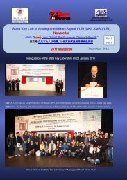
State Key Lab of Analog and Mixed-Signal VLSI (SKL AMS-VLSI)<br />
<strong>Newsletter</strong><br />
Motto: “Locally, from (World) Quality towards (National) Quantity”<br />
座 右 銘 : 立 足 本 土 、 人 才 培 養 , 以 世 界 級 質 量 創 建 國 家 級 規 模<br />
Year 8<br />
No . 8<br />
<strong>2018</strong> Milestones<br />
March 2019<br />
Co-Funded by<br />
Macao Science and Technology<br />
Development Fund (FDCT)<br />
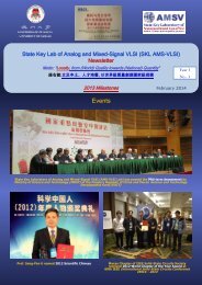
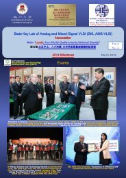
Events<br />
State Key Laboratory of Analog and Mixed-Signal VLSI (SKL AMS-VLSI) participated in the 12th Annual Meeting of the<br />
Committee for China and Macao Cooperation in Science and Technology held in Wuhan, Hubei, China, November 14, <strong>2018</strong>.<br />
State Key Laboratory of Analog and Mixed-Signal VLSI (SKL AMS-VLSI) held the 3rd Academic Committee meeting<br />
on June 12, <strong>2018</strong>.<br />
State Key Laboratory of Analog and Mixed-Signal VLSI (SKL AMS-VLSI) signed a Memorandum of Understanding (MOU)<br />
with International Iberian Nanotechnology Laboratory (INL) from Braga, Portugal, on March 21, <strong>2018</strong>.
E<br />
C<br />
A2<br />
A3<br />
A1<br />
B<br />
D<br />
State-of-the-Art Chips - Designed and Tested in <strong>2018</strong> (32 chips)<br />
CORE: 6.5 × 7 µm 2<br />
Testing<br />
Buffer<br />
530 μm<br />
270 μm<br />
ISSCC 2019<br />
A team of faculty members and students from the SKL AMS-VLSI and ECE/FST, University of Macau (UM) attended the 66 th IEEE<br />
International Solid-State Circuits Conference (ISSCC) in February 2019 in San Francisco, CA, USA, the most competitive conference<br />
in the world in the field of chip design.<br />
8 papers from SKL AMS-VLSI in areas of Data<br />
Converters, RF and Power Management were<br />
accepted and presented at ISSCC 2019, ranking the university<br />
second in the world in microelectronics research, along with the<br />
University of Michigan - Ann Arbor, next only to Intel. This shows<br />
the international recognition of UM and its leading position in the<br />
field in Asia. Besides, the SKLab PhD students received 1 Predoctoral<br />
Achievement Award, 1 Student Research Preview<br />
Award, 2 Student Research Previews and 1 onsite demonstration.<br />
In addition, Prof. Pui-In Mak received his IEEE fellow<br />
certificate at the conference, for his contributions to the fields of<br />
radio frequency and analog circuits. He is the first native of<br />
Macao to receive such prestigious honor.<br />
Pui-In Mak Becomes the 1st Macao Native<br />
Elected IEEE Fellow<br />
Pui-In Mak Appointed by the Chinese<br />
Academy of Sciences as Overseas Expert<br />
Macau, ‘Las Vegas of Asia’, Trades in<br />
Casino Chips for Microchips as Part of<br />
China’s Tech Ambitions<br />
The Institute of Electrical and Electronics<br />
Engineers (IEEE) has released its 2019 fellow<br />
list. Prof. Pui-In Mak from State Key Laboratory<br />
of Analog and Mixed-Signal VLSI (SKL<br />
AMS-VLSI) has made the list, for his contributions<br />
to the fields of radio frequency and<br />
analog circuits. He is the first native of Macao<br />
to receive this prestigious honor. The 2019<br />
list includes 295 new fellows, 30 of whom are<br />
scientists from China. Prof. Mak belongs to<br />
the youngest category (in the 31-39 age<br />
bracket), which is a very rare accomplishment.<br />
Pui-In Mak, Associate Director (research) of<br />
the University of Macau (UM) State Key Laboratory<br />
of Analog and Mixed-Signal VLSI<br />
(SKL AMS-VLSI), who is also a professor in the<br />
Department of Electrical and Computer Engineering,<br />
Faculty of Science and Technology,<br />
attended an event for participants in the 100<br />
and the 1,000 Experts Programs held in<br />
Beijing last year. During the event, he was<br />
appointed a member of the overseas expert<br />
panel of the Chinese Academy of Sciences<br />
(CAS).<br />
“Macau is best known for its casino chips, now it is<br />
also known for its electronics chips,” said Rui P.<br />
Martins, the vice-rector for research at the University<br />
of Macau, which plays host to the city’s two<br />
State Key Laboratories – institutes that China<br />
relies on to conduct scientific research crucial to<br />
national development. “We hope with this system,<br />
with some time, the know-how will be in China …<br />
In 10 years’ time, probably you don’t need to<br />
import from the United States,” Martins believes<br />
that in time, Macau could change the balance of<br />
power between China and the US. SKL AMS-VLSI<br />
has been one of the Asian institutions with the<br />
most inventions at the IEEE ISSCC, also known as<br />
the “Chips Olympics”, in San Francisco.<br />
— in HK SCMP, 16 Jun, <strong>2018</strong><br />
6 New PhD Graduates<br />
6. Yang Jiang, Design of Fully Integrated Fine-Grained Switched-<br />
Capacitor DC-DC Topologies in Bulk CMOS, Jan. 2019.<br />
5. Liu Jianwei, Design Techniques for Energy Efficient ADCs,<br />
Jan. 2019.<br />
4. Xing Dezhi, Advanced Techniques in Analog to Digital<br />
Converters, Jan. 2019.<br />
3. Da Feng, Polyphase Decomposition for Sigma-Delta A/D<br />
Converters, Aug. <strong>2018</strong>.<br />
2. Tantan Zhang, Nano-Watt Class CMOS Interface Circuits for<br />
Wireless Sensor Nodes, Jun. <strong>2018</strong>.<br />
1. Zhiyuan Chen, Efficient Power Management Design for<br />
Energy Harvesting Biomedical Applications, Apr. <strong>2018</strong>.<br />
Pui-In Mak Appointed as<br />
Associate Editor of the<br />
IEEE Journal of Solid-<br />
State Circuits<br />
Man-Kay Law Selected as<br />
IEEE CASS Distinguished<br />
Lecturer 2019-2020<br />
A Joint-Chapter with<br />
University of Harvard in a<br />
Book by Springer
Selected works from each research line<br />
In ISSCC <strong>2018</strong> and Invited JSSC <strong>2018</strong><br />
An Inverse-Class-F CMOS VCO with Intrinsic-High-Q 1st- and<br />
2nd-Harmonic Resonances for 1/f 2 -to-1/f 3 Phase-Noise Suppression<br />
Achieving 196.2dBc/Hz FOM<br />
Chee-Cheow Lim, Jun Yin, Pui-In Mak, Harikrishnan Ramiah, and Rui P. Martins<br />
From Wireless research line<br />
Motivation<br />
This work is an inverse-class-F (class-F −1 )<br />
CMOS oscillator. It features: 1) a single-ended<br />
PMOS-NMOS-complementary architecture to<br />
generate the differential outputs and 2) a transformer-based<br />
two-port resonator to boost the<br />
drain-to-gate voltage gain (AV) while creating<br />
two intrinsic-high-Q impedance peaks at the fundamental<br />
(f LO ) and double (2f LO ) oscillation frequencies.<br />
The enlarged second harmonic voltage<br />
extends the flat span in which the impulse<br />
sensitivity function (ISF) is minimum, and the<br />
amplified gate voltage swing reduces the current<br />
commutation time, thereby lowering the –gm<br />
transistor’s noise-to-phase noise (PN) conversion.<br />
Prototyped in 65-nm CMOS, the class-F −1<br />
oscillator at 4 GHz exhibits a PN of –144.8 dBc/<br />
Hz at a 10-MHz offset, while offering a tuning<br />
range of 3.5–4.5 GHz. The corresponding figure<br />
of merit (FoM) is 196.1 dBc/Hz, and the die area<br />
is 0.14 mm 2 .<br />
Architecture<br />
VCO Topology and Key Waveforms<br />
Implementation<br />
Chip Photo and Measurement Results<br />
Verification<br />
Key Measured Performances
A 0.22-to-2.4V-Input Fine-Grained Fully Integrated Rational Buck-<br />
Boost SC DC-DC Converter Using Algorithmic Voltage-Feed-In<br />
(AVFI) Topology Achieving 84.1% Peak Efficiency at 13.2mW/mm 2<br />
From Wireless research line<br />
Yang Jiang, Man-Kay Law, Pui-In Mak, and Rui P. Martins<br />
In ISSCC <strong>2018</strong> and Invited JSSC <strong>2018</strong><br />
Motivation<br />
Architecture<br />
This work proposes an algorithmic voltage-feed-in (AVFI)<br />
topology capable of systematic generation of any arbitrary<br />
buck–boost rational ratio with optimal conduction loss while<br />
achieving reduced topology-level parasitic loss among the<br />
state-of-the-art works. By disengaging the existing topology<br />
-level restrictions, we develop a cell-level implementation<br />
using the extracted Dickson cell (DSC) and charge-pathfolding<br />
cell (QFC) to minimize the power-stage parasitic<br />
loss, exhibiting a Dickson-like switching pattern. The proposed<br />
partitionable main cell (MC) and auxiliary cell (AC)<br />
architecture achieves fined-grained voltage conversion<br />
ratio (FVCR) reconfiguration with optimal power cell utilization<br />
and reduced control complexity. Implemented in 65-nm<br />
bulk CMOS, the fully integrated switched-capacitor power<br />
converter (SCPC) using 10 MCs and 10 ACs executes a<br />
total of 24 VCRs (11 buck and 13 boost) with wide-range<br />
efficient buck–boost operations through the proposed reference-selective<br />
bootstrapping driver (RSBD). Based on<br />
the AVFI topology, the chip prototype reaches a measured<br />
peak efficiency of 84.1% at a power density of 13.4 mW/<br />
mm 2 over a wide range of input (0.22–2.4 V) and output<br />
(0.85–1.2 V).<br />
Architecture of the Proposed Buck-Boost<br />
SC DC-DC Converter<br />
Implementation<br />
Result<br />
State-of-the-Art Comparison
A 0.6V 13b 20MS/s Two-Step TDC-Assisted SAR ADC with PVT<br />
Tracking and Speed-Enhanced Techniques<br />
Minglei Zhang, Chi-Hang Chan, Yan Zhu, Rui P. Martins<br />
In ISSCC 2019<br />
From Data Conversion and Signal Processing research line<br />
Motivation<br />
Architecture<br />
Implementation<br />
Verification
In VLSI <strong>2018</strong> and JSSC 2019<br />
A 550mW 20kHz BW 100.8dB SNDR Linear-Exponential Multi-Bit Incremental<br />
SD ADC with 256 clock cycles in 65nm CMOS<br />
Biao Wang, Sai-Weng Sin, Seng-Pan U, Franco Maloberti, Rui P. Martins<br />
From Data Conversion and Signal Processing research line<br />
Motivation<br />
This work presents an incremental analog-to-digital<br />
converter (IADC) with a two-phase linear-exponential<br />
accumulation loop. In the linear phase, the loop<br />
works as a first-order structure. The noise-coupling<br />
path is then enabled in the exponential phase thus<br />
boosting the SQNR exponentially with a few number<br />
of clock cycles. The two-phase scheme combines the<br />
advantages of the thermal noise suppression in the<br />
1 st -order IADC and SQNR boosting in the exponential<br />
mode. The uniform-exponential weight function allows<br />
the data weighted averaging (DWA) technique<br />
to work well, leading to the rotation of the multi-bit<br />
DAC mismatch error. Meanwhile, this scheme does<br />
not destroy the notches, which can be utilized to suppress<br />
the line noise. Implemented in 65nm CMOS<br />
under 1.2V supply, the ADC achieves an SNDR/DR<br />
of 100.8dB/101.8dB with 20kHz BW, 550μW &<br />
0.134mm 2 , resulting in Walden/Schreier FoM W /FoM S<br />
of 153fJ/176.4dB, respectively. The differential and<br />
integral nonlinearities are +0.27/-0.27 and +0.84/-<br />
0.81 LSBs, respectively.<br />
Vin<br />
Architecture<br />
Reset<br />
z -1<br />
1-z -1<br />
Exponential<br />
Phase<br />
Reset<br />
(1+ke)z -1<br />
NC Path<br />
DAC<br />
Analog Modulator<br />
Linear Phase<br />
Exponential<br />
Phase<br />
(1-(1+ke)z -1 )eq<br />
-eq<br />
Proposed Linear-Exponential Multi-Bit Incremental ADC and its<br />
timing<br />
Vin<br />
F1d<br />
BS_SW<br />
Di<br />
VRefp<br />
F2d<br />
F1d<br />
CDAC<br />
0.5pF<br />
x16<br />
`Di<br />
VRefn<br />
Chopping Switches<br />
F2d<br />
x16<br />
F2<br />
F1<br />
z -1<br />
Freset<br />
Cf<br />
8pF<br />
Dout<br />
ADC<br />
17 levels<br />
DWA<br />
(a)<br />
1 st order NL Ts<br />
F2D_EN<br />
Di<br />
Reset Exponential<br />
z -1<br />
1-z -1<br />
1 st order<br />
Accumulator<br />
One conversion time N cycles<br />
F1d<br />
VRefp1<br />
F2d<br />
Cff3<br />
(b)<br />
F1D_EN `Di<br />
VRefn1<br />
Cff1<br />
Cff2<br />
20fF<br />
x16<br />
x16<br />
80fF<br />
80fF<br />
Reset<br />
Phase<br />
1<br />
1-(1+ke)z -1<br />
Exp NE Ts<br />
Exponential<br />
Accumulator<br />
N<br />
Ddec<br />
For ke = 1 in Exponential Phase<br />
STF =<br />
1 1<br />
1-z -1 1-2z -1<br />
=(2-1)+(2 2 -1)z -1 +(2 3 -1)z -2 +(2 4 -1)z -3 +...<br />
Digital Filter<br />
F1o2<br />
F1e1<br />
F1<br />
F2<br />
F1e2<br />
F1o1<br />
F2<br />
Cho<br />
320fF<br />
Che<br />
320fF<br />
Cff<br />
(-2z -1 )eq injection<br />
160fF<br />
F1e2<br />
F1o2<br />
F1o1<br />
F1e1<br />
NC (1-2z -1 )eq<br />
F1dd<br />
17 level<br />
Dout<br />
Circuit Implementation<br />
DWA<br />
PSD [dBFS]<br />
320mm<br />
Implementation<br />
0<br />
-50<br />
-100<br />
420mm<br />
-0.9dBFS<br />
Amp1<br />
Cs/Cf<br />
Capacitor Array<br />
Switches<br />
Buffer<br />
DWA<br />
AMP2<br />
Noise<br />
Coupling<br />
CAP Array<br />
Linear-phase DWA/on<br />
SNDR = 73.02 dB<br />
Linear-exponential DWA/off<br />
SNDR = 72.75 dB<br />
Linear-exponential DWA/on<br />
SNDR = 100.8 dB<br />
SFDR=121dB<br />
Flash<br />
Verification<br />
P/fsnyq[PJ]<br />
Area [mm 2 ]<br />
1.E+06<br />
1.E+05<br />
1.E+04<br />
1.E+03<br />
1.E+02<br />
1.E+01<br />
1.E+00<br />
10 20 30 40 50 60 70 80 90 100 110 120<br />
1.E+01<br />
ISSCC <strong>2018</strong><br />
1.E+00 VLSI <strong>2018</strong><br />
ISSCC 1997-2017<br />
1.E-01 VLSI 1997-2017<br />
1.E-02<br />
ISSCC <strong>2018</strong><br />
VLSI <strong>2018</strong><br />
ISSCC 1997-2017<br />
VLSI 1997-2017<br />
FOMW=1fJ/conv-step<br />
FOMS=185dB<br />
This work<br />
This work<br />
1.E-03<br />
10 20 30 40 50 60 70 80 90 100 110 120<br />
SNDR [dB]<br />
Data Source from B. Murmann, "ADC Performance Survey 1997-<strong>2018</strong>," [Online].<br />
Available: http://web.stanford.edu/~murmann/adcsurvey.html<br />
Architecture<br />
Process<br />
Supply<br />
Fs<br />
Bandwidth<br />
Power<br />
Peak SNDR<br />
This Work ISSCC 18 JSSC 15 JSSC 17 ISSCC 18 VLSI 17 ISSCC 16<br />
Linearexponential<br />
Incremental<br />
65nm<br />
1.2V<br />
10.24MHz<br />
20kHz<br />
550mW<br />
100.8dB<br />
3 rd -order<br />
Incremental<br />
180nm<br />
3V<br />
30MHz<br />
100kHz<br />
1.098mW<br />
86.6dB<br />
Two-step<br />
Incremental<br />
65nm<br />
1.2V<br />
192kHz<br />
250Hz<br />
10.7mW<br />
90.8dB<br />
Multi-step<br />
Incremental<br />
180nm<br />
1.5V<br />
642kHz<br />
1kHz<br />
34.6mW<br />
96.8dB<br />
Zoom<br />
ADC<br />
160nm<br />
1.8V<br />
2MHz<br />
1kHz<br />
0.28mW<br />
118.1<br />
Pipelined-<br />
SAR<br />
180nm<br />
1.8V/5V<br />
2MHz<br />
1MHz<br />
11.35mW<br />
99.2dB<br />
Oversampling<br />
SAR<br />
55nm<br />
1.2V<br />
1MHz<br />
1kHz<br />
15.7mW<br />
101dB<br />
Dynamic Range<br />
101.8dB<br />
91.5<br />
99.8dB<br />
99.7dB<br />
120.3<br />
100.5dB<br />
N/A<br />
-150<br />
0 4 8 12 16 20<br />
Frequency [kHz]<br />
FoMw(pJ/conv.) #<br />
FoMs(dB) #<br />
0.153<br />
176.4<br />
0.314<br />
166.2<br />
0.76<br />
164.5<br />
0.32<br />
171.4<br />
0.21<br />
183.6<br />
0.07<br />
178.7<br />
0.0856<br />
179<br />
Area [mm 2 ]<br />
0.134 0.36<br />
0.2 0.5<br />
0.25 3.87 0.072<br />
# FoMW = Power/(2 ENOB *2*BW) ; FoMS = SNDR+10log10(BW/Power)
In IEEE Transactions on Ultrasonics, Ferroelectrics, and Frequency Control <strong>2018</strong><br />
Monolithic Multiband CMUTs for Photoacoustic Computed<br />
Tomography With In Vivo Biological Tissue Imaging<br />
Sio Hang Pun, Yuanyu Yu, Jian Zhang, Jiujiang Wang, Ching-Hsiang Cheng, Kin Fong Lei,<br />
Zhen Yuan and Peng Un Mak<br />
From Biomedical research line<br />
[Editor’s Selection of Articles — December <strong>2018</strong> ]<br />
Motivation<br />
Architecture<br />
In this paper, a monolithic multiband capacitive micromachined<br />
ultrasonic transducer (CMUT) array<br />
was designed and fabricated for the reception of the<br />
wideband PA signals so as to provide high-resolution<br />
images with high-frequency CMUT arrays and present<br />
the high signal-to-noise-ratio major structure<br />
with low-frequency CMUT arrays.<br />
To demonstrate its performance, a phantom experiment<br />
was conducted to show and evaluate the various<br />
qualities of multiresolution images.<br />
In addition, an in vivo mouse model experiment was<br />
also carried out for revealing the multiscale PA imaging<br />
capability with the multiband CMUTs on biological<br />
tissues. From the obtained results, the images from<br />
different CMUT arrays could show the structures of<br />
the mouse brain in different scales.<br />
In addition, the images from the high-frequency<br />
CMUT arrays were able to reveal the major blood<br />
vasculatures, whereas the images from lowfrequency<br />
CMUT arrays showed the gross macroscopic<br />
anatomy of the brain with higher contrast.<br />
Implementation<br />
Verification
Reconfigurable X-Connected Wireless Power Transceiver for Device-to-Device<br />
Wireless Charging<br />
Fangyu Mao, Yan Lu, Seng-Pan U, and Rui P. Martins<br />
In ISSCC <strong>2018</strong><br />
From Integrated Power research line<br />
Motivation<br />
Architecture<br />
Wireless power transfer (WPT) via inductive<br />
coupling is a convenient way to charge<br />
the power-starving portable/wearable devices.<br />
Recently, device-to-device (D2D)<br />
wireless charging was demonstrated,<br />
which expands the WPT applications. Different<br />
from the traditional wireless charging<br />
which gets energy from the AC mains and<br />
has unlimited energy, the D2D charging<br />
sources power from an energy-constrained<br />
battery. Therefore, achieving the maximum<br />
efficiency transfer is a key design issue.<br />
This work proposes an X-connected wireless<br />
power TRX with near-optimum switchtiming-control<br />
schemes, which not only reduces<br />
the circuit components but also<br />
greatly improves the power efficiency.<br />
Now, the power PMOS transistors in both<br />
TX and RX modes are X-connected, forming<br />
a fully-symmetrical structure. Then, the<br />
gate-drive switching loss of the power<br />
PMOS transistors is recycled by the LC<br />
tank.<br />
Implementation<br />
The proposed reconfigurable X-connected<br />
wireless power TRX was fabricated in a<br />
0.35-μm CMOS process with thick metal-4<br />
option. The complete system with one battery<br />
charging another was demonstrated<br />
on ISSCC <strong>2018</strong>, San Francisco, USA.<br />
Verification<br />
Measured AC input voltage, charging current<br />
and output voltage when charging a<br />
4.7-mF capacitor. The maximum charging<br />
current is 0.6A.
LampPort - A Handheld Digital Microfluidic Device for Loop-Mediated<br />
Isothermal Amplification (LAMP)<br />
Liang Wan, Jie Gao, Tianlan Chen, Cheng Dong, Haoran Li, Yan-Zi Wen, Zhao-Rong Lun,<br />
Yanwei Jia, Pui-In Mak, and Rui P. Martins<br />
From Multidisciplinary Research Area (Microfluidics)<br />
In Springer Biomedical Microdevices 2019<br />
Motivation<br />
This work is a handheld, automatic and detection<br />
system-free thermal digital microfluidic (DMF) device<br />
for DNA detection by loop-mediated isothermal amplification<br />
(LAMP). Droplet manipulation and real-time<br />
temperature control systems were integrated into a<br />
handheld device. The control software could be installed<br />
into any tablet and communicate with the device<br />
via Bluetooth. In the experimentation, we loaded<br />
2-μl samples with an electrowetting force into sandwich-structured<br />
DMF chips, thereby considerably reducing<br />
reagent consumptions. After an on-chip LAMP<br />
reaction, we added a highly concentrated SYBR<br />
Green I droplet and mixed it with a reaction droplet to<br />
enable product detection with the naked eye. This<br />
step prevented aerosol contamination by avoiding the<br />
exposure of the reaction droplet to the air. Using a<br />
blood parasite Trypanosoma brucei as a model system,<br />
this system showed similar results as a commercial<br />
thermal cycler and could detect 40 copies per<br />
reaction of the DNA target. This low-cost, compact<br />
device removed the bulky optical system for DNA<br />
detection, thus enabling it to be well suited for POC<br />
testing.<br />
Architecture<br />
Overview of a handheld digital microfluidic (DMF) device<br />
for loop-mediated isothermal amplification (LAMP).<br />
Implementation<br />
Result<br />
End-point evaluation of on-chip LAMP reactions<br />
(a) before and (b) after adding SYBRGreen I.<br />
These images were captured using iPhone 6 (a,<br />
b) under the ambient light and (c) under the<br />
sunlight. The SYBR Green I concentration in (a)<br />
was 1000×. A black adhesive tape was attached<br />
to the bottom of the DMF chip to enhance the<br />
naked-eye visualisation. NTC: no-template control.<br />
POS: positive sample
Technology Transfer Office and Commercialization Activities<br />
<strong>2018</strong> was the 3rd year after the creation of the Technology Transfer Office (TTO). Over the past three years, due to tremendous efforts from TTO on<br />
establishing good interaction with the IC design industry, the number of cooperation research projects between SKL-<strong>AMSV</strong> and companies has grown<br />
consistently. The amount of research funding from industry is estimated to be more than ten times from 2017 to 2019. The industry partners are from<br />
Greater Bay area cities such as Shenzhen, Guangzhou, Zhuhai and also from Beijing. The mainland largest IC design company is one of SKL-<strong>AMSV</strong>’s<br />
cooperation partner.<br />
Industry-Academy Collaboration Projects<br />
1 4<br />
6<br />
A delegation from Huawei visited SKL <strong>AMSV</strong> for discussions<br />
2017 <strong>2018</strong> 2019<br />
Number of Industry-Academy Projects has rapidly grown<br />
Contributing to the Development of Guangdong-Hong Kong-Macau Greater Bay Area<br />
Integrated Circuit Design is one of the strategic key industries in China. At the same time, our state plans to drive Guangdong-Hong Kong-Macau<br />
Greater bay area into an innovation-oriented economic system in 2035. As a State Key Laboratory, SKL-<strong>AMSV</strong> responds to the development direction<br />
of the country with specific actions. In addition to disseminate our technology to regional companies, SKL-<strong>AMSV</strong> has also participated in the establishment<br />
of Guangdong- Hong Kong-Macau Semiconductor Industry Alliance becoming its founding member. Moreover, more resources from SKL-<strong>AMSV</strong><br />
will be allocated to setup the SKL-<strong>AMSV</strong> design center in Hengqin.<br />
The establishment of Guangdong-Hong Kong-Macau<br />
Semiconductor Industry Alliance, with delegations from<br />
Hong Kong, Macau, Shenzhen, Guangzhou and Zhuhai.<br />
Seminar on Macau-Hengqin Industry-University Research<br />
Cooperation, with delegations from UM and Industry<br />
US and International Patents Granted in <strong>2018</strong><br />
1. “A Method for On-Chip Precise Sample Delivery in a Microfluidic System,” International Patent, PCT/UMPT161-<strong>2018</strong>, Jul. <strong>2018</strong>.<br />
2. “Cooperative-Electrode Driving Technique for Droplet-Velocity Improvement of Digital Microfluidic Systems,” US Patent, No. 10,016,759, Jul. <strong>2018</strong>.<br />
3. “A Hybrid STATCOM with Wide Compensation Range and Low DC-Link Voltage,” US Utility patent, No. 9,751,083, Jun. <strong>2018</strong>.<br />
4. " 一 种 检 测 和 分 析 DNA 的 方 法 ," International Patent, PCT/CN<strong>2018</strong>/088762, May <strong>2018</strong>.<br />
5. “Design of a Thyristor Controlled LC Compensator,” US Utility Patent, No. 9,960,599, May. <strong>2018</strong>.<br />
6. “Limit Cycle Oscillation Reduction for Digital Low Dropout Regulators,” US Patent, No. 9946281, Apr. <strong>2018</strong>.<br />
Upholding Scientific Leadership in ISSCC Benchmark in Terms of State-of-The-Art Chips<br />
Academy in China 2011 2012 2013 2014 2015 2016 2017 <strong>2018</strong> 2019 Total<br />
University of Macau 2 1 1 3 2 3 6 7 8 33<br />
HKUST 1 1 2 3 4 3 4 2 1 21<br />
Fudan Univ. 1 1 2 1 0 0 0 2 3 10<br />
Tsinghua Univ. 1 0 0 2 0 1 0 0 2 6<br />
Chinese Acad. Sci. 1 0 1 1 0 0 0 0 0 3<br />
Peking Univ. 0 0 0 0 0 0 0 1 0 1<br />
Chengdu UESTC 0 0 0 0 0 0 0 1 0 1<br />
SJTU 0 0 0 0 0 0 0 0 1 1<br />
Southeast U. 0 0 0 0 0 0 0 0 1 1<br />
Awards and Student Research Previews (PhD)<br />
in 2011 - 2019:<br />
1 x Far-East Best Paper Award (First in China)<br />
7 x SSCS Pre-Doctoral Achievement Awards<br />
2 x ISSCC Silkroad Awards<br />
1 x ISSCC Student Research Preview Award<br />
14 x ISSCC Student Research Preview<br />
New Academics Joined SKL AMS-VLSI in <strong>2018</strong><br />
Assistant Professor<br />
Ka-Fai Un received the B.Sc. degree in electrical engineering from National Taiwan University (NTU), Taipei, Taiwan, in 2007, and the M.Sc. and Ph.D.<br />
degrees in electrical and electronics engineering from the University of Macau (UM), Macao, China. He is currently a Assistant Professor at SKL AMS-<br />
VLSI. He was a Macau Fellow holding a visiting positon in the University College Dublin.<br />
Research Interests: Wireless integrated circuits design, Mathematics.<br />
Lecturer (Macao Fellow)<br />
Weihan Yu received the B.Sc. and M.Sc. degrees in electrical and electronics engineering and Ph.D. degree in electrical and computer engineering from<br />
the University of Macau (UM), Macao, China. He is currently a Lecturer (Macao Fellow) at SKL AMS-VLSI. He will be a Visiting Scholar in the Stanford<br />
University.<br />
Research Interests: Wireless integrated circuits design.
Events and Visits<br />
Visit by a Delegation of China Ministry of Science and<br />
Technology (MOST)<br />
Visit by a Delegation of Guangzhou Science,<br />
Technology and Innovation Commission<br />
Visit by Yan Wu, Vice Mayor of Shenzhen<br />
Government, China<br />
Visit by Wang Lixin, Vice Mayor of Shenzhen<br />
Government, China<br />
Distinguished Lectures and Workshops<br />
“Machine Learning Today and Tomorrow:<br />
Technology, Circuits and System” by<br />
Prof. Boris Murmann,<br />
IEEE Fellow, Professor of Electrical<br />
Engineering, Stanford University, USA<br />
“Software Defined IC and Artificial Intelligence”<br />
by<br />
Prof. Wei Shaojun,<br />
IEEE Fellow, Dean of Institute of<br />
Microelectronics, Tsinghua University, China<br />
“Binaural Hearing Aid System and the<br />
Intelligent Acoustic Signal Processing” by<br />
Prof. Wang Zhihua,<br />
IEEE Fellow, Professor of Tsinghua<br />
University, China<br />
Publications<br />
▓ “Handheld Total Chemical and Biological Analysis Systems,” Springer, <strong>2018</strong>.<br />
Book Chapter<br />
▓ “CMOS Circuits for Biological Sensing and Processing Systems - Micro-NMR on CMOS for Biomolecular Sensing,” Springer, <strong>2018</strong>.<br />
Book<br />
IEEE Conferences – 14 Papers<br />
22nd International Conference on Miniaturized Systems for Chemistry and Life Sciences (µ TAS <strong>2018</strong>), Kaohsiung, Taiwan, China, Nov. <strong>2018</strong><br />
▓ “3D Microstructures to Realize Single Cell Culture on Digital Microfluidic Chip for Precision Medicine”<br />
▓ “On-Chip Pico-Pipette: A Method for Precise Delivery in a DMF system”<br />
44th Annual Conference of the IEEE Industrial Electronics Society (IECON <strong>2018</strong>), Washington D.C., USA, Oct. <strong>2018</strong><br />
▓ “DC-Link Voltage Reduction Design Method for Three-Phase Four-Wire LC-Hybrid Active Powers under Reactive and Unbalanced Current Compensation”<br />
▓<br />
▓<br />
▓<br />
▓<br />
“Voltage Mode Controller Design and Experimental Verification of a Three-Phase Capacitive-Coupling Grid Connected Inverter in PV System”<br />
“A Power Quality Indexes Measurement System Platform with Remote Alarm Notification”<br />
“Selective Power Management Control for Hybrid Active Power Filter”<br />
“Comparisons of Different Hybrid Inverters for Power Quality Compensation with/without Active Power Injection”<br />
▓ “Design and Analysis of Single-Phase Adaptive Passive Part Coupling Hybrid Active Power Filter (HAPF)”<br />
10th IEEE PES Asia-Pacific Power and Engineering Conference (APPEEC <strong>2018</strong>), Sabah, Malaysia, Oct. <strong>2018</strong><br />
▓ “The Analysis of DC-Link Voltage, Compensation Range, Cost, Reliability and Power Loss for Shunt (Hybrid) Active Power Filters”<br />
15th International Conference on Synthesis, Modeling, Analysis and Simulation Methods and Applications to Circuit Design (SMACD <strong>2018</strong>), Prague, Czech<br />
Republic, Jul. <strong>2018</strong><br />
▓ “Design and Optimization of a Class-C/D VCO for Ultra-Low-Power IoT and Cellular Applications”<br />
9th Asia-Pacific Conference of Transducers and Micro-Nano Technology (APCOT <strong>2018</strong>), Hong Kong, China, Jun. <strong>2018</strong><br />
▓ “In-Minutes Polymerase Chain Reaction with Specific DNA Amplification On Digital Microfluidics with Sloppy Temperature Control”<br />
IEEE International Conference on Electron Devices and Solid-State Circuits (EDSSC), Shenzhen, China, Jun. <strong>2018</strong><br />
▓ “In-Minutes Polymerase Chain Reaction with Specific DNA Amplification On Digital Microfluidics with Sloppy Temperature Control”<br />
<strong>2018</strong> International Symposium on VLSI Design, Automation and Test (<strong>2018</strong> VLSI-DAT), Hsinchu, Taiwan, China, Apr. <strong>2018</strong><br />
▓ “A 6.78 MHz Active Voltage Doubler with Near-Optimal On/Off Delay Compensation for Wireless Power Transfer Systems”<br />
23rd Asia and South Pacific Design Automation Conference (ASP-DAC <strong>2018</strong>), Jeju City, South Korea, Jan. <strong>2018</strong><br />
▓ “A Dual-Output SC Converter with Dynamic Power Allocation for Multi-Core Application Processors” [University LSI Design Contest Special Feature Award]
SCI Journals – 54 Papers (6 in 2019)<br />
▓ “LampPort: A Handheld Digital Microfluidic Device for Loop-Mediated Isothermal Amplification (LAMP),” Biomedical Microdevices, Jan. 2019.<br />
▓ “A 0.044-mm 2 0.5-to-7-GHz Resistor-Plus-Source-Follower-Feedback Noise-Cancelling LNA Achieving a Flat NF of 3.3±0.45 dB,” IEEE Transactions on CAS II: Express Briefs, Jan. 2019.<br />
▓ “A 0.0056-mm 2 -4249-dB-FoM All-Digital MDLL using a Block-Sharing Offset-Free Frequency-Tracking Loop and Dual Multiplexed-Ring VCOs,” IEEE Journal of Solid-State Circuits, Jan. 2019.<br />
▓ “Many-Objective Sizing Optimization of a Class-C/D VCO for Ultralow-Power IoT and Ultralow-Phase-Noise Cellular Applications,” IEEE Transactions on Very Large Scale Integration (TVLSI)<br />
Systems, Jan. 2019.<br />
▓ “Analysis of Reference Error in High-Speed SAR ADCs with Capacitive DAC,” IEEE Transactions on Circuits and Systems I: Regular Papers, Jan. 2019.<br />
▓ “Experimental Verifications of Low Frequency Path Gain (PG) Channel Modeling for Implantable Medical Device (IMD),” IEEE Access, Jan. 2019.<br />
▓ “Algorithmic Voltage-Feed-In Topology for Fully Integrated Fine-Grained Rational Buck-Boost Switched-Capacitor DC-DC Converters,” IEEE Journal of Solid-State Circuits, Dec. <strong>2018</strong>. [Invited<br />
Paper]<br />
▓ “An Inverse-Class-F CMOS Oscillator with Intrinsic-High-Q First Harmonic and Second Harmonic Resonances,” IEEE Journal of Solid-State Circuits, Dec. <strong>2018</strong>.<br />
▓ “Process Compensated BJT-Based CMOS Temperature Sensor with a ± 1.5 °C (3σ) Batch-to-Batch Inaccuracy,” IET Electronics Letters, Nov. <strong>2018</strong>.<br />
▓ “Nano-Ampere Low-Dropout Regulator Designs for IoT Devices,” IEEE Transactions on Circuits and Systems I: Regular Papers, Nov. <strong>2018</strong>.<br />
▓ “A 0.19 mm 2 10b 2.3 GS/s 12-Way Time-Interleaved Pipelined-SAR ADC in 65-nm CMOS,” IEEE Transactions on Circuits and Systems I: Regular Papers, Nov. <strong>2018</strong>.<br />
▓ “Missing-Code-Occurrence Probability Calibration Technique for DAC Nonlinearity with Supply and Reference Circuit Analysis in a SAR ADC,” IEEE Transactions on Circuits and Systems I: Regular<br />
Papers, Nov. <strong>2018</strong>.<br />
▓ “Low-Phase-Noise Wideband Mode-Switching Quad-Core-Coupled mm-wave VCO Using a Single-Center-Tapped Switched Inductor,” IEEE Journal of Solid-State Circuits, Nov. <strong>2018</strong>.<br />
▓ “A 220-MHz Bondwire-Based Fully-Integrated KY Converter with Fast Transient Response under DCM Operation,” IEEE Transactions on CAS I: Regular Papers, Nov. <strong>2018</strong>.<br />
▓ “Gain Error Calibrations for Two-Step ADCs: Optimizations Either in Accuracy or Chip Area,” IEEE Transactions on Very Large Scale Integration (TVLSI) Systems, Nov. <strong>2018</strong>.<br />
▓ “A Wideband Inductorless dB-Linear Automatic Gain Control Amplifier Using a Single-Branch Negative Exponential Generator for Wireline Applications,” IEEE Transactions on Circuits and Systems I:<br />
Regular Papers, Oct. <strong>2018</strong>.<br />
▓ “A Fully Integrated Low-Dropout Regulator with Differentiator-Based Active Zero Compensation,” IEEE Transactions on Circuits and Systems I: Regular Papers, Oct. <strong>2018</strong>.<br />
▓ “A Low-Power Compression-Based CMOS Image Sensor with Microshift-Guided SAR ADC ,” IEEE Transactions on Circuits and Systems – Part II: Express Briefs , Oct. <strong>2018</strong>.<br />
▓ “A 5.35-mW 10-MHz Single-Opamp Third-Order CT ΔΣ Modulator with CTC Amplifier and Adaptive Latch DAC Driver in 65-nm CMOS,” IEEE Journal of Solid-State Circuits, Oct. <strong>2018</strong>.<br />
▓ “A 10-MHz Bandwidth Two-Path Third-Order ΣΔ Modulator with Cross-Coupling Branches,” IEEE Transactions on Circuits and Systems II: Express Briefs, Oct. <strong>2018</strong>.<br />
▓ “A 14-bit Split-Pipeline ADC with Self-Adjusted Opamp-Sharing Duty-Cycle and Bias Current,” IEEE Transactions on Circuits and Systems II: Express Briefs, Oct. <strong>2018</strong>.<br />
▓ “A Reconfigurable and Extendable Digital Architecture for Mixed Signal Power Electronics Controller,” IEEE Transactions on Circuits and Systems II: Express Briefs, Oct. <strong>2018</strong>.<br />
▓ “Review and Selection Strategy for High Accuracy Modeling of PWM Converters in DCM,” Hindawi Journal of Electrical and Computer Engineering, Oct. <strong>2018</strong>.<br />
▓ “Advanced Power Electronic Converters and Power Quality Conditioning,” Journal of Electrical and Computer Engineering, Oct. <strong>2018</strong>.<br />
▓ “0.45-V 5.4-nW Switched-Capacitor Bandgap Reference with Intermittent Operation and Improved Supply Immunity,” IET Electronics Letters, Oct. <strong>2018</strong>.<br />
▓ “Ambient RF Energy Harvesting System: A Review on Integrated Circuit Design,” Springer Analog Integrated Circuits and Signal Processing, Sep. <strong>2018</strong>.<br />
▓ “A 36-Gb/s 1.3-mW/Gb/s Duobinary-Signal Transmitter Exploiting Power-Efficient Cross-Quadrature Clocking Multiplexers with Maximized Timing Margin,” IEEE Transactions on Circuits and Systems<br />
I: Regular Papers, Sep. <strong>2018</strong>.<br />
▓ “A Regulation-Free Sub-0.5 V 16-/24-MHz Crystal Oscillator with 14.2-nJ Startup Energy and 31.8-µW Steady-State Power,” IEEE Journal of Solid-State Circuits, Sep. <strong>2018</strong>.<br />
▓ “A Coin-Battery-Powered LDO-Free 2.4-GHz Bluetooth Low-Energy Transmitter with 34.7% Peak System Efficiency,” IEEE Transactions on Circuits and Systems II: Express Briefs, Sep. <strong>2018</strong>.<br />
▓ “A Hardware-Efficient Feedback Polynomial Topology for DPD Linearization of Power Amplifiers: Theory and FPGA Validation,” IEEE Transactions on CAS I - Regular Papers, Sep. <strong>2018</strong>.<br />
▓ “Analysis, Control, and Design of a Hybrid Grid-Connected Inverter for Renewable Energy Generation with Power Quality Conditioning,” IEEE Transactions on Power Electronics, Aug. <strong>2018</strong>.<br />
▓ “An Assay for Systematically Quantifying the Vestibulo-Ocular Reflex to Assess Vestibular Function in Zebrafish Larvae,” Frontiers in Cellular Neuroscience, Aug. <strong>2018</strong>.<br />
▓ “Hybrid Structure of Static VAR Compensator and Hybrid Active Power Filter (SVC//HAPF) for Medium Voltage Heavy Loads Compensation,” IEEE Transactions on Industrial Electronics (TIE), Jun.<br />
<strong>2018</strong>.<br />
▓ “A 0.18-V 382-μW Bluetooth Low-Energy Receiver Front-End with 1.33-nW Sleep Power for Energy-Harvesting Applications in 28-nm CMOS,” IEEE Journal of Solid-State Circuits, Jun. <strong>2018</strong>.<br />
▓ “A Digital LDO with Co-SA Logics and TSPC Dynamic Latches for Fast Transient Response,” IEEE Solid-State Circuits Letters, Jun. <strong>2018</strong>.<br />
▓ “Design Considerations of Distributed and Centralized Switched-Capacitor Converters for Power Supply On-Chip,” IEEE Journal of Emerging and Selected Topics in Power Electronics, Jun. <strong>2018</strong>.<br />
▓ “Overview of Recent Development on Wireless Sensing Circuits and Systems for Healthcare and Biomedical Applications,” IEEE Journal on Emerging and Selected Topics in Circuits and Systems,<br />
Jun. <strong>2018</strong>.<br />
▓ “Hybrid Structure of Static VAR Compensator and Hybrid Active Power Filter (SVC//HAPF) for Medium Voltage Heavy Loads Compensation,” IEEE Transactions on Industrial Electronics, Jun. <strong>2018</strong>.<br />
▓ “Analysis of Common Mode Interference and Jitter of Clock Receiver Circuits with Improved Topology,” IEEE Transactions on Circuits and Systems I - Regular Papers, Jun. <strong>2018</strong>.<br />
▓ “Multi-Functional Hybrid Structure of SVC and Capacitive Grid Connected Inverter (SVC//CGCI) for Active Power Injection and Non-Active Power Compensation,” IEEE Transactions on Industrial<br />
Electronics (TIE), May <strong>2018</strong>.<br />
▓ “A SAW-Less Tunable RF Front End for FDD and IBFD Combining an Electrical-Balance Duplexer and a Switched-LC N-Path LNA,” IEEE Journal of Solid-State Circuits , May <strong>2018</strong>.<br />
▓ “Turning On/Off The Anti-Tumor Effect of the Au Cluster via Atomically Controlling Its Molecular Size,” ACS Nano, Apr. <strong>2018</strong>.<br />
▓ “Minimizing Inverter Capacity Design and Comparative Performance Evaluation of SVC-Coupling Hybrid Active Power Filters,” IEEE Transactions on Power Electronics (TPEL), Apr. <strong>2018</strong>.<br />
▓ “Nano-Watt Class Energy-Efficient Capacitive Sensor Interface with On-Chip Temperature Drift Compensation,” IEEE Sensors Journal , Apr. <strong>2018</strong>.<br />
▓ “A 0.083-mm 2 25.2-to-29.5 GHz Multi-LC-Tank Class-F234 VCO with a 189.6-dBc/Hz FOM,” IEEE Solid-State Circuits Letters, Apr. <strong>2018</strong>.<br />
▓ “A Two-Way Interleaved 7-b 2.4-GS/s 1-Then-2 b/Cycle SAR ADC with Background Offset Calibration,” IEEE Journal of Solid-State Circuits, Mar. <strong>2018</strong>.<br />
▓ “Monolithic Multiband CMUTs for Photoacoustic Computed Tomography With In Vivo Biological Tissue Imaging,” IEEE Transactions on Ultrasonics, Ferroelectrics, and Frequency Control, Mar.<br />
<strong>2018</strong>.<br />
▓ “Quick and Cost-Efficient A/D Converter Static Characterization using Low-Precision Testing Signal,” Microelectronics Journal - Elsevier, Feb. <strong>2018</strong>.<br />
▓ “A 0.032-mm 2 0.15-V 3-Stage Charge-Pump Scheme Using a Differential Bootstrapped Ring-VCO for Energy-Harvesting Applications,” IEEE Transactions on Circuits and Systems II: Express Briefs,<br />
Feb. <strong>2018</strong>.<br />
▓ “Passive Noise Shaping in SAR ADC with Improved Efficiency,” IEEE Transactions on VLSI Systems, Feb. <strong>2018</strong>.<br />
▓ “Analysis in the Effects of Operation Voltage Range in Flexible DC Control on Railway HPQC Compensation Capability in High-Speed Co-Phase Railway Power,” IEEE Transactions on Power Electronics,<br />
Feb. <strong>2018</strong>.<br />
▓ “Time-Efficient BER Estimation Approach Using Jitter Characteristics for HBC Channel,” IET Science, Measurement & Technology, Jan. <strong>2018</strong>.<br />
▓ “An Analog-Assisted Tri-Loop Digital Low-Dropout Regulator,” IEEE Journal of Solid-State Circuits, Jan. <strong>2018</strong>.<br />
▓ “A 0.7–2.5 GHz, 61% EIRP System Efficiency, Four-Element MIMO TX System Exploiting Integrated Power-Relaxed Power Amplifiers and an Analog Spatial De-Interleaver,” IEEE Transactions on Circuits<br />
and Systems I: Regular Papers, Jan. <strong>2018</strong>.<br />
Major IEEE Solid-State Circuits Conferences – 21 Papers<br />
IEEE Asian Solid-State Circuits Conference (ASSCC <strong>2018</strong>), Tainan, Taiwan, China, Nov. <strong>2018</strong><br />
▓ “A 7b 2 GS/s Time-Interleaved SAR ADC with Time Skew Calibration Based on Current Integrating Sampler” [Highlighted Paper]<br />
▓ “A 2.4-GHz Single-Pin Antenna Interface RF Front-End with a Function-Reuse Single-MOS VCO-PA and a Push-Pull LNA”<br />
▓ “An Integrated DC-DC Converter with Segmented Frequency Modulation and Multiphase Co-Work Control for Fast Transient Recovery”<br />
IEEE European Solid-State Circuits Conference (ESSCIRC <strong>2018</strong>), Dresden, Germany, Sep. <strong>2018</strong><br />
▓ “A 39mW 7b 8GS/s 8-way TI ADC with Cross-linearized Input and Bootstrapped Sampling Buffer Front-end”<br />
IEEE Symposium on VLSI Circuits (VLSIC), Honolulu, USA, Jun. <strong>2018</strong><br />
▓ “A 77dB SNDR 12.5MHz Bandwidth 0-1 MASH ΣΔ ADC Based on the Pipelined-SAR Structure”<br />
▓<br />
“A 2pJ/Pixel/Direction MIMO Processing Based CMOS Image Sensor for Omnidirectional Local Binary Pattern Extraction and Edge Detection”<br />
▓ “A 550µW 20kHz BW 100.8dB SNDR Linear-Exponential Multi-Bit Incremental Converter with 256-cycles in 65nm CMOS” [Travel Grant Award] [Invited Special Issue in JSSC]<br />
IEEE International Symposium on Circuits and Systems (ISCAS), Florence, Italy, May <strong>2018</strong><br />
▓ “Design and Control of an Integrated 3-Level Boost Converter under DCM Operation”<br />
▓<br />
▓<br />
“A Single-Stage Current-Mode Active Rectifier with Accurate Output-Current Regulation for IoT”<br />
“A Dual-Loop Digital LDO Regulator with Asynchronous-Flash Binary Coarse Tuning”<br />
▓ “A 0.4V 6.4µW 3.3MHz CMOS Bootstrap Relaxation Oscillator with ±0.71% Frequency Deviation from -30°C to 100°C for Wearable and Sensing Applications”<br />
IEEE International Solid-State Circuits Conference (ISSCC <strong>2018</strong>), San Francisco, CA, USA, Feb. <strong>2018</strong><br />
▓ “A 0.2V Energy-Harvesting BLE Transmitter with a Micropower Manager Achieving 25% System Efficiency at 0dBm Output and 5.2nW Sleep Power in 28nm CMOS”<br />
▓ “A 0.22-to-2.4V-Input Fine-Grained Fully-Integrated Rational Buck-Boost SC DC-DC Converter Using Algorithmic Voltage-Feed-In (AVFI) Topology Archiving 84.1% Peak Efficiency at 13.2μW/mm 2 ” [Invited<br />
Special Issue in JSSC]<br />
▓ “A Regulation-Free Sub-0.5V 16/24MHz Crystal Oscillator for Energy Harvesting BLE Radios with 14.2nJ Startup Energy and 31.8uW Steady-State Power”<br />
▓ “A 0.4V 430nA Quiescent Current NMOS Digital LDO with NAND-Based Analog-Assisted Loop in 28nm CMOS”<br />
▓ “A Reconfigurable Cross-Connected Wireless-Power Transceiver for Bidirectional Device-to-Device Charging with 78.1% Total Efficiency”<br />
▓ “A 0.0056mm 2 All-Digital MDLL Using Edge Re-Extraction, Dual Ring-VCOs and a 0.3mW Block-Sharing Frequency-Tracking Loop Achieving 292fsrms Jitter and -249dB FoM” [Invited Special Issue in JSSC]<br />
▓ “An Inverse-Class-F CMOS VCO with Intrinsic-High-Q 1 st - and 2 nd -Harmonic Resonances for 1/f 2 -to-1/f 3 Phase Noise Suppression Achieving 196.2dBc/Hz FoM” [Invited Special Issue in JSSC]<br />
▓ “A 14-bit Split Pipeline ADC with Self-Adjusted Opamp-Sharing Duty Cycle” [Student Research Preview]<br />
▓ “A Coin-Battery-Powered Regulation-Free 2.4-GHz Bluetooth Low-Energy Transmitter (TX)” [Student Research Preview]<br />
▓ “A 430frms 2.4GHz Ring-Oscillator PLL with Backend Discrete-Time Phase Noise Cancellation Achieving 240.5dB Jitter-FoM” [Student Research Preview]<br />
The first spin-off of the SKLab AMS-VLSI, named Digi Fluidic and led by<br />
2 of our PhD graduates, started operation in Innovalley, Hengqin, China.<br />
State Key Laboratory of Analog and Mixed-Signal VLSI / UM<br />
http://www.amsv.umac.mo