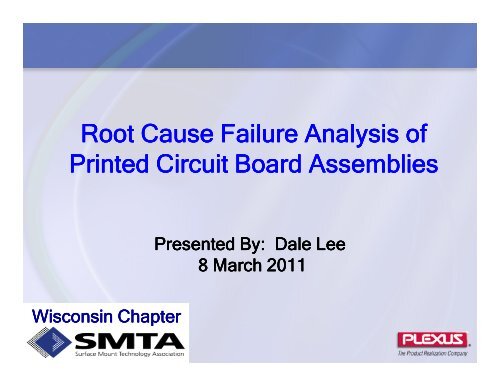
Root Cause Failure Analysis of Printed Circuit Board ... - SMTA
Root Cause Failure Analysis of Printed Circuit Board ... - SMTA
Root Cause Failure Analysis of Printed Circuit Board ... - SMTA

You also want an ePaper? Increase the reach of your titles
YUMPU automatically turns print PDFs into web optimized ePapers that Google loves.
<strong>Root</strong> <strong>Root</strong> <strong>Root</strong> <strong>Cause</strong> <strong>Cause</strong> <strong>Failure</strong> <strong>Failure</strong> <strong>Analysis</strong> <strong>Analysis</strong> <strong>of</strong><br />
<strong>of</strong><br />
<strong>Printed</strong> <strong>Printed</strong> <strong>Circuit</strong> <strong>Circuit</strong> <strong>Board</strong> <strong>Board</strong> Assemblies<br />
Assemblies<br />
Wisconsin Wisconsin Chapter<br />
Chapter<br />
Presented Presented By: By: Dale Dale Lee<br />
Lee<br />
8 8 March March 2011<br />
2011
What do you mean 0% first pass yield?<br />
Photo Courtesy <strong>of</strong> G. Toren<br />
My My My My process process process process is is is is in in in in control control control control , , , , so so so so what what what what happened?<br />
happened?<br />
happened?<br />
happened?
Today’s Electronic Designs<br />
• Component Packages Are Getting Smaller<br />
• 0603 > 0402 > 0201>01005<br />
• BGA > CSP > WL-CSP > ?<br />
• Assembly Design Density Is Increasing<br />
• Tighter Component to Component Spacing<br />
(Spacing Smaller Than 0.020” Common)<br />
• Smaller Copper (Pad) Interconnections<br />
• Assembly Process Margins Are Tighter<br />
• Thermal Balance @ Pad Level Is Critical<br />
(Trace/Via Connection Size to Pads)<br />
• Component Placement Accuracy<br />
(The Thickness Of A Piece <strong>of</strong> Paper Can<br />
Be Difference Between 100% Rework or<br />
High Yields)
Effects <strong>of</strong> Mfg Environment<br />
• Elements From Manufacturing Facility May<br />
Contribute Defects. These include:<br />
– Process Equipment Materials<br />
– ESD Control (Smock/Wrist Strap)<br />
– Paper Work<br />
– Component Packaging<br />
– Facility Environment<br />
– Clothing<br />
– Operators (Hair)
Component Issues - Warpage<br />
• Higher Lead Free Solder Solidification and Process<br />
Temperatures, Increases The Amount Of Thermal<br />
Expansion Mismatch Of Components Which Can Increase<br />
Amount Of Component Warping During Assembly<br />
Process<br />
• May Require Redesign Of Package (Material Selection) For Thermal<br />
Mass And Expansion Balance.
Component/PCB Warpage Impacts<br />
Split Split Planes/Unused<br />
Planes/Unused<br />
Planes/Unused<br />
Pad Pad Removal:<br />
Removal:<br />
• Localize Changes In<br />
Thickness/Coplanarity<br />
Of PCB<br />
• Potential Opens From<br />
Tilted Components<br />
(Teeter-Totter Effect)<br />
• Potential Opens From<br />
“Dropped” Solder<br />
Connection<br />
• Potential Reduced<br />
Reliability From<br />
Stretched Solder Joints<br />
Some Photos Courtesy <strong>of</strong> Amkor
Component Issues – Decreasing Pitch<br />
0.2 mm<br />
0.4 mm<br />
0.8 mm<br />
Potential Potential Issues:<br />
Issues:<br />
1.0 mm<br />
– Paste Volume Control<br />
– Component/PCB Flatness<br />
• Internal Split Plane<br />
• NFP Removal Impacts<br />
– Component/PCB Warpage<br />
1.27 mm
LGA/QFN Package Assembly<br />
• Trace Routing Under Component<br />
Create Localized Height Variations<br />
– Stand<strong>of</strong>f Height Variation<br />
• Leadless Devices Are More<br />
Sensitive To PCB/Component<br />
Flatness/Warpage<br />
– Received Condition<br />
– In-process Condition (During<br />
Reflow/Rework Solder Process)<br />
LGA Package<br />
BGA Package
LGA Pad Design<br />
Solder Solder Mask Mask Defined Defined Non Non-Solder Non Solder Solder Mask Mask Defined<br />
Defined<br />
• Solder Solder Solder wicking wicking wicking around around around around NSMD NSMD pads pads produce produce significantly significantly lower<br />
lower<br />
molten molten solder solder height.<br />
height.<br />
• Solder Solder Solder mask mask defined defined defined pads pads should should be be used used for for LGA LGA and and 0.4mm 0.4mm &<br />
&<br />
smaller smaller pitch pitch pitch BGA/CSP BGA/CSP BGA/CSP packages. packages.<br />
packages.
Component Issues – LGA & QFN<br />
Potential Potential Issues:<br />
Issues:<br />
– Land Pattern Design<br />
• Pad Size Uniformity (SMD vs NSMD)<br />
– Paste Volume Control<br />
• Pad to Pad Volume<br />
• Pad to Design Defined Volume<br />
– Component/PCB Flatness<br />
• Internal Split Plane<br />
• NFP Removal Impacts<br />
– Component/PCB Warpage<br />
– Decrease Component Stand<strong>of</strong>f Height<br />
• Decreased Reliability
% PAD SIZE INCREASE<br />
60<br />
50<br />
40<br />
30<br />
20<br />
10<br />
Trace Routing Impacts Solder Joint<br />
0<br />
EFFECTIVE PAD SIZE ANALYSIS<br />
4 10 15 20<br />
WIDTH OF TRACE 10 Mil Nom 15 Mil Nom 20 Mil Nom<br />
10 Mil Max 15 Mil Max 20 Mil Max<br />
Increased Increased Mounting<br />
Mounting<br />
Pad Pad Size Size Affected Affected By:<br />
By:<br />
• Number Of Trace<br />
Connections To Each Pad<br />
• Width Of Trace<br />
Connections To Each Pad<br />
• Size <strong>of</strong> Pad<br />
– Small Pads Have Less<br />
Margin<br />
• Uniformity Of Trace<br />
Egress Direction<br />
– Some Package Types Are<br />
More Sensitive Than Others<br />
• Uniformity Of Trace Sizes
Trace Routing Impacts Solder Joint<br />
• Gradient Of Different Trace Sizes<br />
• Localized Concentrated Large Trace<br />
Connections Increase Defect Potential<br />
Concentrations Of Design Variability Can Create:<br />
Solder Bridge, Open Connection, Insufficient Solder, Tilted<br />
Components
Component Pad - Thermal Imbalance<br />
• Multiple Trace Connections<br />
– Number Of Trace Connections<br />
Per Pad<br />
– Uniformity Across All Pads On<br />
Single Component<br />
• Solder Mask Defined Pad<br />
• Increased Soldering Defects<br />
– Delayed Reflow Across SMT<br />
Components<br />
• Tombstone Components<br />
• “Ball in Socket” Area Array<br />
Component
Component Pad - Thermal Imbalance<br />
• Small Passive Component Pad Design<br />
– Mixed Solder Mask Defined<br />
• Multiple/Large Trace<br />
• Exposed Plane<br />
– Smaller Component Package, The<br />
Greater The Impact
Thick Copper Design<br />
A A CTE CTE Mismatch Mismatch Between Between Copper Copper And And FR FR-4 FR 4 Exists<br />
Exists<br />
• Copper = 18ppm<br />
• FR-4 = 15-16ppm<br />
• As Copper Gets Thicker, It Has Greater And Greater Influence Over Post<br />
Lamination Dimensions Of The Resulting Substrate<br />
Rolled Rolled , , Annealed Annealed Copper Copper Reacts Reacts Differently Differently Differently Than Than ED ED ED Copper<br />
Copper<br />
• Design Influences On Net Shrinkage Become Far More Significant<br />
Standard Scaling Factors (That Compensate Net Shrinkage Effects) Do<br />
Not Apply!<br />
More More More Resin Resin Is Is Required Required To To “Fill” “Fill” “Fill” Etched Etched Out Out Areas<br />
Areas<br />
• “In-plane” CTE Increases With % Resin Content<br />
• “Another Complication To Net Shrinkage Prediction”<br />
• Resin Rich Package = Higher Z-axis CTE = Greater Sensitivity To Thermal<br />
Excursions, Assembly In Particular.<br />
• Heavy Copper Substrates Generally Require More Heat Input To Assemble<br />
• Reliability!
Thick Copper Design<br />
• Heavy Heavy Copper, Copper, Embedded Embedded In In Glass Glass Epoxy, Epoxy, Can Can Result Result<br />
Result<br />
In In Nonplanar Nonplanar Conditions Conditions On On On The The Surface Surface Of Of The The<br />
The<br />
Substrate<br />
Substrate<br />
• The The Heavier Heavier The The Copper, Copper, The The Worse Worse The The Effect<br />
Effect<br />
• In In In In Multi Multi-layer Multi Multi-layer Multi layer layer Applications, Applications, Local Local Local Local Local Areas Areas With With “Stacked”<br />
“Stacked”<br />
Copper, Copper, Beside Beside Areas Areas That That Are Are Etched Etched Out, Out, Can<br />
Can<br />
Result Result Result In In Extreme Extreme Non Non-planarities<br />
Non Non planarities<br />
• PCB PCB Fabrication Fabrication Industry Industry Typically Typically Refers Refers To To This This As<br />
As<br />
“Image “Image Transfer” Transfer”<br />
Transfer”
Thick Copper Design<br />
Lack Lack Of Of Planarity Planarity<br />
Planarity<br />
Reduces Reduces The<br />
The<br />
Effective Effective Resolution Resolution<br />
Resolution<br />
Of Of The The Fabrication<br />
Fabrication Fabrication Fabrication<br />
Process, Process, Limiting<br />
Limiting<br />
Feature Feature Size<br />
Size
Heavy Copper Lamination<br />
• Imaging Imaging Resist Resist Resist Thickness Thickness Is Is 1.3 1.3 1.3 - 2mils. 2mils. At At At Some Some Some Point, Point, Image<br />
Image<br />
Transfer Transfer Transfer Interferes Interferes With With The The Imaging Imaging Resists Resists Ability Ability To To “Conform” “Conform”<br />
“Conform”<br />
To To The The Lack Lack Of Of Planarity Planarity Planarity On On The The Surface Surface Of Of The The Substrate. Substrate.<br />
• This This Lack Lack Of Of Planarity Planarity Also Also Reduces Reduces The The Effective Effective Resolution Resolution Of<br />
Of<br />
The The System, System, Limiting Limiting Feature<br />
Feature
Copper Etch Process<br />
• H H = = = Height Height <strong>of</strong> <strong>of</strong> Copper Copper Trace Trace<br />
Trace<br />
• Etch Factor = 2H / (W W max - W W W min) min)<br />
min)<br />
• Etch Factor Should Be Larger Than 1.0
Etched Trace Design Considerations<br />
� Thinner Copper Produces More Precise Geometries on<br />
Lines Less Than 0.005” in Width<br />
� Actual Conductor Shape is Close to a Trapazoid<br />
� Copper Thickness is Slightly Reduced After PCB Processing
Pad Size Reduction<br />
Current Procedures For Applying Uniform Etch Compensation<br />
Values Across All Surface Features Are Inadequate.<br />
Below Illustrate A Near Exponential Reduction In Pad Size As<br />
The Pad Gets Smaller, For Both Round And Square Pads In<br />
Either Orientation.
Warpage & Thermal Pr<strong>of</strong>ile Issues<br />
May May May Require Require Require Change Change In In In Production<br />
Production<br />
Process<br />
Process<br />
• Tooling To Bridge Warpage Gap.<br />
(Increased Solder Paste Volume Application, etc.<br />
Reflow Pallets For <strong>Board</strong> Support)<br />
• Reflow Pr<strong>of</strong>ile To Bridge Component<br />
Warpage Gap.<br />
(Decreased Thermal Change Rate And Delta T<br />
Vertically In Component Package – Reduce Surface<br />
To Cooler Location Temperature Delta - TCE<br />
Induced Warpage)<br />
• Reflow Pr<strong>of</strong>ile To Bridge PCB Warpage Gap.<br />
(Decreased Thermal Change Rate And Delta T<br />
Vertically In PCB – Reduce Surface To Cooler<br />
Location Temperature Delta - TCE Induced<br />
Warpage)<br />
Large ∆T across <strong>Board</strong>
• Voids in Solder Joints<br />
– Unfilled Via in Pad<br />
• Provide Flat Pad With<br />
Filled/Plated Closed Via<br />
• Solder Joint Formation<br />
– Thermal Connection<br />
• Plane Connection<br />
• Multiple Connections<br />
• Stacked Via<br />
– Solder Volume<br />
• Via Location - Edge<br />
Micro-Via in Pad<br />
No Via<br />
Unfilled Via’s<br />
Plated Closed & Filled Via
Artwork Artwork Feature Feature Feature Positional<br />
Positional<br />
Tolerances Tolerances Increase<br />
Increase<br />
PCB Tolerances<br />
– Inner/Outer Layer Shrinkage<br />
(Technology / Material<br />
Dependant)<br />
– Some Materials Do Not Shrink<br />
Uniformly<br />
– PCB Size – TCE Impact On<br />
Dimensional Measurements<br />
– Fabrication & Depanelization<br />
Material Movement / PCB<br />
Fabrication Tolerances Artwork<br />
Registration<br />
• As Fabricated<br />
• Pre-routing <strong>of</strong> Array<br />
• After Depanelization
Stencil Tolerances<br />
Artwork Artwork Feature Feature Positional<br />
Positional<br />
Tolerances Tolerances Increase<br />
Increase<br />
– Fabrication Tolerances Artwork<br />
Registration<br />
• Etched Feature Position<br />
• Etched Feature Size<br />
• Etched Feature Quality<br />
• Etched Feature Directional Etch<br />
– Stencil Print Directional<br />
Compensation Orientation
Stencil To PCB Alignment<br />
• Smaller Components<br />
Decrease Total PCB<br />
& Assembly Process<br />
Tolerance<br />
• Minor Misalignment<br />
Can Impact Process<br />
Yields<br />
3 mil 6 mil
Offset Paste – Normal Placement<br />
Photo Courtesy <strong>of</strong> Juki Automation
Match Tooling Design To Parts<br />
PCB to Stencil Pad Positional Deviation<br />
Measurements No Adjustments<br />
“Using Stencil: Design to Reduce SMT Defects”, SMT, April 2006<br />
• Normal Manufacturing Process<br />
Variability May Exceed Allowable<br />
Assembly Process Tolerance For<br />
High Yield, Reliable Assembly<br />
• Matched Tooling (Stencils) To Materials<br />
(PCB) May Be Required<br />
PCB to Stencil Pad Positional Deviation<br />
Measurements With Scaling Adjustments
Match Placement To Paste<br />
• Slight Offset Of Solder<br />
Paste And Component<br />
Placement May Improve<br />
Soldering Yields<br />
– Paste and Placement<br />
Must Have Same Offset<br />
– Tombstone Passives<br />
– BGA Voiding
Matched Offset – Paste & Part<br />
Photo Courtesy <strong>of</strong> Juki Automation
Solder Paste Printing Volume<br />
Air Bubble In Solder Paste Bead<br />
Open/Unwetted LGA Connection<br />
Leadless Device Usage<br />
Increase (DFN, QFN,<br />
LCC LGA) & Ultra-fine<br />
Pitch Components<br />
Impacts:<br />
Tighter Tolerance On Solder<br />
Paste Volume – Thinner Stencil<br />
Increased Uniformity Of Paste<br />
Volume Across Component<br />
(Pad to Pad)<br />
Paste Volume/Pad Trace Egress<br />
Direction Impact<br />
– Some Package Types Are<br />
More Sensitive Than Others
Low Component<br />
Stand-<strong>of</strong>f Height<br />
• Tilted Component<br />
• Open Joints (stand<strong>of</strong>f<br />
from PCB)<br />
• Misalignment<br />
Component Types<br />
• Leadless<br />
– QFN, DFN, Passives,<br />
etc.<br />
• Fine Pitch Area Array<br />
– BGA, WL-CSP, CSP,<br />
etc.<br />
Silk Screen Design
Internal PCB Impacts<br />
Number Of Layer Connections to<br />
Plated Through Hole<br />
– Increased Number Of Layer<br />
Connections Increases Thermal<br />
Mass Of Plated Through Hole<br />
– Increased Number Of Plane<br />
Layer Connections Greatly<br />
Increases Thermal Mass Of<br />
Plated Through Hole<br />
– Increase Thermal Pad Isolation<br />
To Improve Solder Flow To<br />
Topside<br />
Issues Include:<br />
– PTH Hole Fill
What To Do?<br />
• Increase Solder Temperature?<br />
Lead Free Solder Issue<br />
Higher Solder Temperatures Or<br />
Increased Solder Dwell Times<br />
Create Problems With Pads On<br />
Solder Side<br />
* Dr. S. Zweiger, Solectron GMBH, Productronica Green Day, November 2005
Wave Solder & Rework Issues<br />
0.005” Trace Dissolution in<br />
30 Seconds<br />
Limit Effects Of Copper Dissolution<br />
– Use Lower Dissolution<br />
Rate Solder Alloy<br />
Modified SAC Alloy<br />
(Sb, Ni, Zn, Ge, In, Etc)<br />
Non-SAC Alloy<br />
(Sn/Cu/Ni, Etc)<br />
– Pad Trace Connection<br />
• Tear Drop<br />
• Snow Man Connection<br />
• Wide Trace<br />
• Greater Than 0.010”<br />
• PCB Photo Courtesy <strong>of</strong> Cookson – Alpha Metals<br />
• Byle, Jean & Lee, “Copper Dissolution Rate in Pb-Free Soldering Fountain Systems”, <strong>SMTA</strong>-I 2006<br />
Original SnPb<br />
SAC 305 SN100C<br />
After wave soldering, 265 o C<br />
solder temperature, 12 seconds<br />
contact time
Lead Free Solder Spread<br />
• Stencil Alignment<br />
Tolerance <strong>of</strong> Solder<br />
Paste To SMT Pad<br />
May Be Critical For<br />
Achieving Good<br />
Tin-Lead Paste<br />
Manufacturing Yields<br />
(Dependant Upon PCB<br />
Surface Finish)<br />
• Example – OSP Finish<br />
Alpha Metals, SMT Mag Webcast, Jan 2006<br />
Lead Free Paste
PCB Finish Vs Solder Spread<br />
– OSP<br />
– Immersion Silver<br />
– Immersion Tin<br />
– ENIG<br />
Amount Amount Of Of Of Lead Lead Free Free Solder Solder Wicking Wicking Wicking Is Is Dependant<br />
Dependant<br />
Upon Upon Finish<br />
Finish
Tin-Lead Vs Lead Free Wicking<br />
Depending Upon The<br />
Pairing Of PCB<br />
Surface Finish And<br />
Component Lead<br />
Finish, The Amount<br />
Of Solder Wicking /<br />
Spread Can Induce<br />
or Reduce Solder<br />
Defect Formation.<br />
Lead Free Tin-Lead
Defects <strong>Cause</strong>d By Improper Thermal Balance<br />
Wave Solder Process<br />
Thermal Shock<br />
Damage<br />
LED<br />
lead<br />
LED<br />
• Increase thermal<br />
pad isolation<br />
• Balance number<br />
connections for<br />
component per<br />
each plated through<br />
hole<br />
• Uniformity <strong>of</strong> trace<br />
size connection to<br />
component plated<br />
through hole
Lead To Hole Clearance<br />
• Lead Lead Lead Free Free Soldering Soldering<br />
Soldering<br />
– Lead Clearance Minimum May<br />
Increase<br />
– Increasing <strong>Board</strong> Thickness May<br />
Further Increase Lead To Hole<br />
Clearance (Aspect Ratio)<br />
– Larger Holes Create Less Voids<br />
• Smaller Smaller Lead Lead To To Hole<br />
Hole<br />
Clearance Clearance Clearance Decreases<br />
Decreases<br />
Shrinkage Shrinkage Holes Holes / / Hot Hot Tear<br />
Tear<br />
Joints<br />
Joints<br />
IPC-A-610D, Fig. 5.67
Through Hole Pad Design<br />
• Square Pads Should Not Be Used On<br />
Solder Side<br />
– Increased Pad Lifting*<br />
– Increased Solder Defect –<br />
Bridge/Flag/Web<br />
• Decrease Component / Top Side Pad<br />
Size**<br />
– Reduced Fillet Lifting<br />
* Dr. S. Zweiger, Solectron GMBH, Productronica Green Day, November 2005<br />
** K Puttlitz, K Stalter, “Handbook <strong>of</strong> Lead-Free Solder Technology For Microelectronic Assembly”, pp 628, Fig 48
Through Hole Pad Design<br />
• All Pads Should Be Same Shape<br />
– Oval or Round<br />
– Pin 1 square pad should not be used on<br />
solder side<br />
– In some situation legend ink in between<br />
pads can help to minimize solder bridges<br />
• High Density Components (< 2mm<br />
Pitch)<br />
– Pads Should Be Oval In Shape<br />
– Staggered Pad Designs Should Be Used To<br />
Enhance Solder Joint Formation On Exit<br />
Side Of Component
Effect <strong>of</strong> <strong>Board</strong> Thickness<br />
On Topside Fillet Formation<br />
0.062”<br />
0.100”<br />
0.150”<br />
<strong>Board</strong> Thickness<br />
• <strong>Board</strong> thickness<br />
increase thermal mass<br />
<strong>of</strong> plated through-hole<br />
• Increase thermal pad<br />
isolation to improve<br />
solder flow to the top<br />
side<br />
• Increase lead hole<br />
clearance (aspect ratio)<br />
to improve solder flow<br />
to top side
Effect <strong>of</strong> Lead Length on Topside Fillet Formation<br />
1.0mm Φ hole, 0.45mm Φ lead<br />
Lead Length:<br />
0.040”/1mm<br />
Lead Length:<br />
0.080”/2mm<br />
Lead Length:<br />
0.120”/3mm<br />
• Lead Length protrusion<br />
too long on solder side:<br />
– Only a small quantity <strong>of</strong><br />
solder retained in<br />
soldering area, solder<br />
flow downwards along<br />
component lead<br />
• Lead Length protrusion<br />
too short on solder side:<br />
– Only a small quantity <strong>of</strong><br />
solder can transferred,<br />
and the heat transfer<br />
maybe insufficient
Solder Mask Selection<br />
Matte Finish Solder Mask Has<br />
Increase Surface Energy To Hold<br />
Flux To The <strong>Board</strong> (More Flux<br />
For Solder Joint Formation)<br />
Dull/Low Reflection Appearance<br />
Glossy Finish Solder Mask Has<br />
Low Surface Energy to Flux To<br />
The <strong>Board</strong> (Less Flux For Solder<br />
Joint Formation – Solder Balls,<br />
Icicles, Flags, etc.)<br />
Highly Reflective Appearance<br />
Preferred<br />
Preferred<br />
Not Not Preferred<br />
Preferred
Cleaning<br />
“Remember it is not the cleanliness <strong>of</strong> the<br />
entire board that causes the electrical<br />
failure but the amount <strong>of</strong> residue between<br />
two pads on a critical circuit the define the<br />
cleanliness <strong>of</strong> the assembly.”<br />
Terry Munson, President/Senior Technical Consultant, Foresite<br />
Ask the Experts, <strong>Circuit</strong>net.com, 7 Jan. 2008
Cleaning Chemistry Compatibility<br />
• Cleaning Chemistries Must Work<br />
With Tight Component Spacing<br />
– Component To Component Spacing<br />
– Component Stand-<strong>of</strong>f Height<br />
• Compatible With Greater Diversity Of<br />
Materials<br />
– PCB’s<br />
• Substrate Materials<br />
• Solder Mask<br />
• Silk Screen Ink<br />
• Pad Finish<br />
– Component Materials<br />
• Package<br />
• Seals<br />
• Marking Inks<br />
– Solder
Careful – Clean May Not Be Reliable<br />
Solder Paste Bridge Between Pads on BGA After Reflow and Cleaning
Inspectability – AOI, AXI, HVI<br />
• Accessibility to Solder Joints –AOI, HVI,<br />
AXI<br />
– Component Spacing – Line <strong>of</strong> Sight<br />
– Solder Fillet Length<br />
• Masking <strong>of</strong> Solder Joints<br />
– Solder Connections Under Component Body<br />
– Insufficient Separation Between Solder Joints<br />
• Stacked Component Vertical Separation<br />
• PCB Thickness<br />
– Material Density; X-ray Permeability<br />
– Side to Side Shadowing<br />
• Insufficient Background Contrast<br />
– Component Package to PCB<br />
– Solder Joint to PCB
Field Return Issue<br />
Cracked Cap Issue<br />
• Capacitor Functional <strong>Failure</strong><br />
– Cracked Component<br />
• What is root cause?
Cracked Cap Issue<br />
• PCA Is Assembled In<br />
Panelized Form<br />
• PCA Is Depanelized<br />
Using A V-Score<br />
Slicing System<br />
• No Indication Of<br />
Issue At ICT &<br />
Functional Test<br />
Fig.1
Cracked Cap Issue<br />
• Functional Test Required<br />
Mounting Assembly In RF<br />
Test Unit Fixture<br />
• Fixture Did Not Have PCA<br />
Eject Mechanism In<br />
Fixture – Bending Of PCA<br />
To Extract From Test<br />
Fixture Cracked<br />
Capacitor.
Source Of Contamination<br />
What is Source <strong>of</strong> Whiskers in Solder Joints at PCB Interface Surface?<br />
1. Solder Paste<br />
2. Stencil Printer<br />
3. Reflow<br />
4. PCB Finish<br />
5. Thermal Aging
DFX <strong>Analysis</strong> S<strong>of</strong>tware<br />
• Minimize the number <strong>of</strong><br />
revision spins to bring a<br />
new design to<br />
production release<br />
• Lower the cost to<br />
manufacture<br />
• Improve the reliability <strong>of</strong><br />
a design<br />
• Reduce the amount <strong>of</strong><br />
time spent on supplier<br />
“call-backs”<br />
• Work with all major PCB<br />
layout tools
DFX S<strong>of</strong>tware Flexibility<br />
• Concurrent DFX<br />
Resolves Issues At<br />
The Lowest<br />
Possible Cost<br />
• S<strong>of</strong>tware Flexibility<br />
Should Allow For<br />
Multiple Points Of<br />
Access Into The<br />
Design Process
DFX <strong>Analysis</strong> Results<br />
• <strong>Analysis</strong> Results<br />
Should Be Easy<br />
To Review And<br />
Intuitive To Any<br />
Reviewer<br />
• Issues<br />
Presented With<br />
Severity Level<br />
Ranking
DFX PCA-PCB S<strong>of</strong>tware Systems<br />
Mentor -Valor Valor Computerized<br />
Computerized<br />
Systems<br />
Systems<br />
• Mentor<br />
(Enterprise 3000, Trilogy 5000)<br />
Mentor – Router Solutions<br />
• Mentor<br />
(BOM Explorer, CAMCAD)<br />
• Siemens Siemens UGS UGS - Technomatix<br />
Technomatix<br />
(Assembly Expert)<br />
• Aegis Aegis S<strong>of</strong>tware<br />
S<strong>of</strong>tware<br />
• SMS<br />
(<strong>Circuit</strong>CAM – Fusion)<br />
SMS<br />
(Linecontrol)<br />
• Zuken<br />
Zuken<br />
(CR-5000 <strong>Board</strong> Modeler)<br />
• Downstream Downstream Downstream Technologies<br />
Technologies<br />
(CAM350)<br />
• ADIVA<br />
ADIVA<br />
(DRC – Design <strong>Analysis</strong>)<br />
• Graphicode<br />
Graphicode<br />
(GC-CAM, GC-Place, GC-ICT)<br />
• Wise Wise S<strong>of</strong>tware<br />
S<strong>of</strong>tware<br />
(Gerbtool)<br />
• Lavenir<br />
Lavenir<br />
(Viewmate)
DFX PCA Test S<strong>of</strong>tware Systems<br />
Mentor -Valor Valor Computerized<br />
Computerized<br />
Systems<br />
Systems<br />
• Mentor<br />
(Enterprise 3000, Trilogy 5000)<br />
Mentor – Router Solutions<br />
• Mentor<br />
(CAMCAD)<br />
• Siemens Siemens UGS UGS - Technomatix<br />
Technomatix<br />
(Test Expert)<br />
• Teradyne<br />
Teradyne<br />
(D2B Alchemist, D2B Strategist)<br />
• Digitaltest<br />
Digitaltest<br />
(C-Link)<br />
• Agilent<br />
Agilent<br />
(Access Consultant)<br />
• Aster Aster Technology<br />
Technology<br />
(Testway)
DFX Mechanical S<strong>of</strong>tware Systems<br />
<strong>Analysis</strong> <strong>Analysis</strong> S<strong>of</strong>tware S<strong>of</strong>tware<br />
S<strong>of</strong>tware<br />
• Boothroyd Boothroyd Boothroyd and and Dewhurst<br />
Dewhurst<br />
(DFMA)<br />
• Geometric Geometric Ltd.<br />
Ltd.<br />
(DFMPro)<br />
• Galorath<br />
Galorath<br />
(SEER)<br />
Design Design S<strong>of</strong>tware<br />
S<strong>of</strong>tware<br />
• PTC<br />
PTC<br />
(Pro/Engineer)<br />
• Autodesk<br />
Autodesk<br />
(AutoCAD)<br />
Dessault<br />
Dessault<br />
• Dessault<br />
(Solidworks , Catia,<br />
Delmia)<br />
• Siemens<br />
Siemens<br />
(NX - SDRC)
Data Format Flexibility<br />
• Fabrication & Electrical Design Information<br />
– <strong>Board</strong> Fabrication Data - Gerber (274D, 274X), Drill Files<br />
(Excellon), etc.<br />
– CAM Tools - ODB++, GenCAD, GenCAM, FATF, etc.<br />
– CAD Tools - Cadence, Mentor, Zuken, Altium, etc.<br />
– Net Lists - IPC-D-356<br />
• Assembly Information<br />
– BOM/AVL/Component Placement - ASCII, Excel, Word, etc.<br />
– Drawings - DXF, HPGL, Gerber, PDF, Postscript, HTML, etc.<br />
• Mechanical Designs<br />
– Design Data –STEP, IGES, DXF/DWG, VRML, etc.
Closing Thought<br />
“We can’t solve problems by using the same kind <strong>of</strong><br />
thinking we used when we created them.”<br />
Albert Einstein<br />
Don’t Don’t Forget Forget About About About Reflow Reflow Process Process Induced<br />
Induced<br />
Warpage/Coplanarity Warpage/Coplanarity Issues.<br />
Issues.
Thank You!<br />
Questions Questions<br />
Questions<br />
Dale Dale Lee Lee<br />
Lee<br />
Dale.Lee@Plexus.Com<br />
Dale.Lee@Plexus.Com