Cadence DFM services Datasheet - Cadence Design Systems
Cadence DFM services Datasheet - Cadence Design Systems
Cadence DFM services Datasheet - Cadence Design Systems

Create successful ePaper yourself
Turn your PDF publications into a flip-book with our unique Google optimized e-Paper software.
<strong>Cadence</strong> <strong>DFM</strong> Services<br />
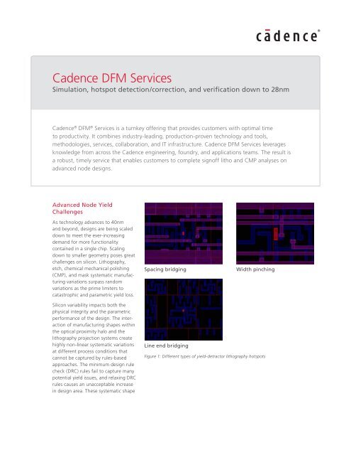
Simulation, hotspot detection/correction, and verification down to 28nm<br />
<strong>Cadence</strong> ® <strong>DFM</strong> ® Services is a turnkey offering that provides customers with optimal time<br />
to productivity. It combines industry-leading, production-proven technology and tools,<br />
methodologies, <strong>services</strong>, collaboration, and IT infrastructure. <strong>Cadence</strong> <strong>DFM</strong> Services leverages<br />
knowledge from across the <strong>Cadence</strong> engineering, foundry, and applications teams. The result is<br />
a robust, timely service that enables customers to complete signoff litho and CMP analyses on<br />
advanced node designs.<br />
Advanced Node Yield<br />
Challenges<br />
As technology advances to 40nm<br />
and beyond, designs are being scaled<br />
down to meet the ever-increasing<br />
demand for more functionality<br />
contained in a single chip. Scaling<br />
down to smaller geometry poses great<br />
challenges on silicon. Lithography,<br />
etch, chemical mechanical polishing<br />
(CMP), and mask systematic manufacturing<br />
variations surpass random<br />
variations as the prime limiters to<br />
catastrophic and parametric yield loss.<br />
Silicon variability impacts both the<br />
physical integrity and the parametric<br />
performance of the design. The interaction<br />
of manufacturing shapes within<br />
the optical proximity halo and the<br />
lithography projection systems create<br />
highly non-linear systematic variations<br />
at different process conditions that<br />
cannot be captured by rules-based<br />
approaches. The minimum design rule<br />
check (DRC) rules fail to capture many<br />
potential yield issues, and relaxing DRC<br />
rules causes an unacceptable increase<br />
in design area. These systematic shape<br />
Spacing bridging Width pinching<br />
Line end bridging<br />
Figure 1: Different types of yield-detractor lithography hotspots
Wafer-Level<br />
Variation<br />
Within-Chip<br />
Variation<br />
Chip<br />
Surface<br />
Wafer<br />
Surface<br />
variations are dependent on specific<br />
layout shape context, and result in<br />
predictable catastrophic errors such as<br />
necking (opens) and bridging (shorts).<br />
These yield limiting hotspots must be<br />
detected and fixed prior to tapeout.<br />
The CMP process introduces issues such<br />
as dishing and erosion, which can lead to<br />
potential yield and performance problems<br />
including copper pooling and excessive<br />
copper loss. Rule-based dummy-fill<br />
insertion or tiling is done on the design<br />
database prior to tapeout. However, in<br />
advanced CMP processes, wide wires can<br />
experience more dishing than narrow<br />
wires, and in some layout configurations<br />
narrow wires can be shorted when they<br />
are on top of two large plates due to the<br />
extra residue from the large plates. CMP<br />
can also impact lithography. Areas with<br />
high or low surface height can cause<br />
defocusing issue in the above layers;<br />
hence, severe topography variations can<br />
cause printability issues.<br />
Because of increasing design costs and<br />
time-to-market pressures, a re-design or<br />
a few-weeks’ delay caused by poor yield<br />
can result in the loss of a critical market<br />
window opportunity.<br />
Oxide Loss<br />
Isolated<br />
Thin-Lines<br />
Dishing<br />
Isolated<br />
Wide-Lines<br />
Erosion<br />
Dense<br />
Array<br />
Thin-Lines<br />
Total Copper Loss<br />
Dense<br />
Array<br />
Wide-Lines<br />
Figure 2: Wafer-level variation due to CMP can lead to topology hotspots or variations<br />
<strong>Design</strong> For Manufacturing<br />
(<strong>DFM</strong>)<br />
The motivation on the manufacturing side<br />
is clear; good <strong>DFM</strong> enables early ramp to<br />
good yield or the fastest time to market<br />
for a design.<br />
<strong>DFM</strong> checks bring manufacturingawareness<br />
to the IC design flow. The<br />
most essential one is lithography process<br />
check (LPC) to detect and correct<br />
systematic litho yield-limiting issues<br />
during design. Model-based litho hotspot<br />
Yield (%)<br />
IC <strong>Design</strong><br />
<strong>Cadence</strong> <strong>DFM</strong> Services<br />
detection is silicon-accurate and can<br />
validate design manufacturability and<br />
account for complex two-dimensional<br />
lithography and mask effects. LPC also<br />
provides design teams with invaluable<br />
early insights and allow them to reduce<br />
physical variability that could severely<br />
impact the performance of the design.<br />
With <strong>DFM</strong> tools integration into digital<br />
and custom implementation flows, a<br />
unified <strong>DFM</strong> flow consisting of modelbased<br />
lithography checks and modelbased<br />
CMP checks can deliver early<br />
prevention, detection, and fixing, so as to<br />
meet the stringent design cycle times.<br />
Turnkey litho and CMP hotspot<br />
analysis service for 40-28nm designs<br />
<strong>Cadence</strong> offers best-in-class <strong>DFM</strong> <strong>services</strong><br />
that include LPC and CMP verification<br />
for 40nm to 28nm nodes. The goal is to<br />
enable design teams to effectively detect<br />
yield-limiting litho or CMP hotspots and<br />
fix them during the IC design phase prior<br />
to tapeout.<br />
Litho process check (LPC)<br />
LPC predicts the silicon image of the<br />
design shapes and detects where the<br />
fidelity between silicon and design<br />
intent is problematic, or where printability<br />
is too challenging and induces<br />
too much variability. LPC is model-based<br />
and silicon-accurate, and can validate<br />
design manufacturability and account for<br />
complex two-dimensional lithography<br />
Desired<br />
Volume<br />
Ramp<br />
Scale and<br />
Complexity<br />
Volume<br />
Ramp<br />
Schedule<br />
www.cadence.com 2<br />
With <strong>DFM</strong><br />
Systematic Defects<br />
~ Time to Market<br />
Figure 3: Earlier ramp to yield with <strong>DFM</strong><br />
Random<br />
Defects<br />
~ Die Price
and mask effects. The tool uses a foundry<br />
qualified litho model and must simulate<br />
all the physical shapes as fast as possible<br />
without compromising accuracy. It should<br />
identify and reduce design sensitivity by<br />
predicting and reducing shape variations.<br />
Printability hotspots vary from bridging<br />
(short), pinching (open), contact overlap,<br />
transistor variations, etc. <strong>Design</strong>-side<br />
litho analysis provides design teams with<br />
invaluable early insights and allows them<br />
to reduce physical variability that could<br />
severely impact yield and the performance<br />
of the design.<br />
Chemical mechanical polishing<br />
(CMP) check<br />
CMP checks take into account multi-level<br />
and long-range effects. CMP hotspots are<br />
shown as a density heat map. This helps<br />
designers understand the root cause of<br />
the CMP issues which are mainly caused<br />
by insufficient metal fill implementation<br />
or too much variation between high and<br />
low density areas of the block or chip.<br />
The correction of the density imbalance<br />
can be done by incrementally altering the<br />
metal fill already implemented manually,<br />
or automatically with intelligent fill-aware<br />
tools and followed by signoff timing<br />
optimization loops.<br />
Flexibility to choose<br />
IC designers can either purchase qualified<br />
<strong>DFM</strong> tools or rely on a qualified <strong>DFM</strong><br />
service offering. The advantages of<br />
owning a tool are obvious, if multiple<br />
designs are being developed and machine<br />
resources are available.<br />
A <strong>DFM</strong> service model is preferred when<br />
a design team desires zero ramp time,<br />
minimal tool learning, and no IT burden.<br />
This is where <strong>Cadence</strong> <strong>DFM</strong> Services aims<br />
to deliver the best cost of ownership and<br />
technical expertise. <strong>Cadence</strong> <strong>DFM</strong> Services<br />
team uses foundry-qualified tools:<br />
<strong>Cadence</strong> Litho Physical Analyzer (LPA), the<br />
“golden” engine for 40nm lithography<br />
process checking (LPC), and <strong>Cadence</strong><br />
CMP Predictor, the industry-leading CMP<br />
analysis solution.<br />
<strong>Cadence</strong> <strong>DFM</strong> Services infrastructure<br />
uses the latest foundry litho and CMP<br />
models for 40-28nm nodes. It leverages<br />
the cloud infrastructure and the compute<br />
power of hundreds of central processing<br />
Proven<br />
Expertise<br />
Secure<br />
Infrastructure<br />
Best<br />
Cost-of-<br />
Ownership<br />
<strong>Cadence</strong><br />
<strong>DFM</strong><br />
Services<br />
units (CPUs) assembled to provide timely<br />
completion of full-chip LPC or CMP<br />
checks on all required layers to deliver the<br />
fastest turnaround time. The hardware<br />
infrastructure can easily scale to support<br />
advanced node design needs—whether<br />
it’s supporting a few early pipe-cleaner<br />
jobs or multiple large designs concurrently.<br />
A state-of-the-art IT and security<br />
infrastructure further ensure that the<br />
customer design data is secure and<br />
protected from unauthorized access.<br />
Leveraging the Breadth of<br />
<strong>Cadence</strong> Expertise<br />
Fastest<br />
Turnaround<br />
Time<br />
Foundry<br />
Golden<br />
Engines<br />
Figure 4: <strong>Cadence</strong> offers <strong>services</strong> as well as<br />
fully qualified solutions<br />
The setup and initiation process is<br />
secure and simple. Customers ship their<br />
encrypted design database (in GDSII or<br />
OASIS format) to a secure, customerspecific<br />
drop box, and receive the analysis<br />
back within days. The <strong>DFM</strong> Services<br />
team provides consultation and detailed<br />
reports, which include the hotspot<br />
locations with X, Y coordinates and show<br />
deviation from the required width or<br />
spacing in a necking or bridge hotspot<br />
location. <strong>DFM</strong> Services also provides<br />
layout-modification guidelines for the<br />
hotspot, which customers can follow to<br />
fix the weak layout topology. The optimal<br />
fixing methodology is to leverage the<br />
automated fixing flow in custom and<br />
digital flows where supported.<br />
The result of the turnkey signoff <strong>DFM</strong><br />
service provides businesses multiple<br />
advantages, including:<br />
• End-to-end <strong>DFM</strong> signoff analysis, which<br />
ensures design manufacturability<br />
<strong>Cadence</strong> <strong>DFM</strong> Services<br />
• Reduced total cost of ownership for<br />
design teams via no investment in <strong>DFM</strong><br />
tools or multi-CPU IT infrastructure or<br />
human time<br />
• Secure infrastructure, which has been<br />
tested and is highly reliable and scalable<br />
• <strong>Cadence</strong> expertise leveraging<br />
production-proven tools, methodologies,<br />
processes, and use models to<br />
provide the fastest turnaround time<br />
Benefits<br />
• Best total cost of ownership: no<br />
investment in software tools, multi-CPU<br />
infrastructure, or learning new tools<br />
• Efficient access: provides priority<br />
turnkey access to foundry “golden” LPC<br />
analysis both prior to and at tapeout<br />
• Reduced schedule risk: allows customer<br />
to verify block-level LPC and CMP<br />
compliance early with a “pipe cleaner”<br />
• Optimal time to results: harnesses 100s<br />
of dedicated CPUs/run in our server<br />
farm for fast turnaround time<br />
• Security: leverages a highly reliable<br />
and state-of-the-art IT and security<br />
infrastructure, which ensures protection<br />
from unauthorized access<br />
• Leverages <strong>Cadence</strong> expertise: offers<br />
many years of experience and<br />
combined resources of <strong>Cadence</strong> <strong>Design</strong><br />
Services<br />
• Low-risk learning experience: provides<br />
a learning experience for designers to<br />
understand <strong>DFM</strong> while designing with<br />
advanced process nodes<br />
• Automated repair: output report<br />
enables automated fixing in digital and<br />
custom implementation flows<br />
<strong>DFM</strong> Tool Infrastructure For LPC<br />
Leveraging the foundry “golden”<br />
litho hotspot analyzer<br />
<strong>DFM</strong> Services uses <strong>Cadence</strong> Litho Physical<br />
Analyzer to facilitate the LPC. Litho<br />
Physical Analyzer is the silicon-proven,<br />
full-chip lithography verification solution<br />
that improves manufacturability, yield,<br />
and design convergence in the chip design<br />
flow. It has been the first to qualify and<br />
www.cadence.com 3
Figure 5: Litho hotspot identified on the design<br />
database<br />
meet the accuracy requirements and is the<br />
“golden” engine at the world’s leading<br />
foundry for the 40nm process node.<br />
CMP Check With <strong>Cadence</strong> CMP<br />
Predictor<br />
CMP Predictor provides full-chip, multilevel<br />
interconnect topography predictions<br />
for the copper CMP process. <strong>Cadence</strong><br />
CMP Predictor accurately predicts the<br />
impact points or hotpsots, like copper<br />
pooling for example, and how they can be<br />
minimized during the design process.<br />
Areas with high or low surface height<br />
can cause defocusing issues in the<br />
above layers. For these reasons, severe<br />
topography variations can cause printability<br />
issues. <strong>DFM</strong> Services’ CMP analysis<br />
reports help designers understand the<br />
root cause of CMP issues, which is mainly<br />
due to insufficient metal fill or too much<br />
difference between high- and low-density<br />
areas of the block or chip. The density<br />
imbalance can be corrected by incrementally<br />
altering the metal fill manually or<br />
automatically with intelligent fill-aware<br />
tools and followed by signoff timing<br />
optimization loops.<br />
Summary<br />
<strong>Cadence</strong> <strong>DFM</strong> Service includes:<br />
• Litho process check (LPC) for 40-28nm<br />
nodes<br />
– LPC is run on cells, blocks, and<br />
full-chip SoCs<br />
– Comprehensive report includes<br />
hotspots and locations<br />
Figure 6: Guidelines to help designers fix the identified yield detractor hotspots<br />
– <strong>Design</strong> layout fixing guidelines for<br />
use with third-party implementation<br />
tools<br />
– Output file for automated fixing with<br />
Encounter and Virtuoso tools<br />
– Incremental re-check to ensure no<br />
new hotspots have been created<br />
• Chemical mechanical polishing (CMP)<br />
check for 28nm<br />
Custom<br />
Implementation<br />
Foundry-Certified<br />
Models/Tech File<br />
<strong>Cadence</strong> <strong>DFM</strong> Services<br />
– Run on blocks (>1mm2) and full-chip<br />
SoCs<br />
– Comprehensive report with topology<br />
hotspots and locations<br />
– <strong>Design</strong> layout fixing guidelines<br />
– Output file for automated fixing with<br />
physical verification/DRC tools<br />
– Incremental re-check to ensure no<br />
new variations have been created<br />
Digital<br />
Implementation<br />
GDSII GDSII/DEF<br />
Contours<br />
Electrical Variability<br />
Analysis<br />
Litho Physical<br />
Analyzer<br />
Hotspots<br />
HIF File<br />
Fixing<br />
Guidelines<br />
Figure 7: Litho Physical Analyzer supports both digital and custom litho analysis<br />
www.cadence.com 4<br />
ECO
CMP model<br />
Foundry validated<br />
Custom<br />
Implementation<br />
More Information<br />
To get more information on how we can<br />
customize our <strong>services</strong> for you, please<br />
email us at dfmservice@cadence.com<br />
Digital<br />
Implementation<br />
GDSII GDSII<br />
Thickness<br />
Map<br />
CMP<br />
Predictor<br />
RC Extraction DRC Metal Fill<br />
Figure 8: CMP Predictor performs model-based CMP analysis<br />
Hotspots<br />
Figure 9: Sample outputs from CMP Predictor<br />
<strong>Cadence</strong> <strong>DFM</strong> Services<br />
<strong>Cadence</strong> is transforming the global electronics industry through a vision called EDA360.<br />
With an application-driven approach to design, our software, hardware, IP, and <strong>services</strong> help<br />
customers realize silicon, SoCs, and complete systems efficiently and profitably. www.cadence.com<br />
© 2011 <strong>Cadence</strong> <strong>Design</strong> <strong>Systems</strong>, Inc. All rights reserved. <strong>Cadence</strong>, the <strong>Cadence</strong> logo, Encounter, and Virtuoso are registered trademarks of<br />
<strong>Cadence</strong> <strong>Design</strong> <strong>Systems</strong>, Inc. All others are properties of their respective holders.<br />
21923 9/11 IW/MK/MV/PDF