High-throughput maskless lithography - Sematech
High-throughput maskless lithography - Sematech
High-throughput maskless lithography - Sematech

You also want an ePaper? Increase the reach of your titles
YUMPU automatically turns print PDFs into web optimized ePapers that Google loves.
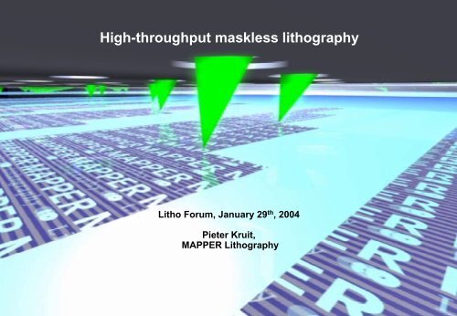
<strong>High</strong>-<strong>throughput</strong> <strong>maskless</strong> <strong>lithography</strong><br />
Litho Forum, January 29 th , 2004<br />
Pieter Kruit,<br />
MAPPER Lithography
Maskless <strong>lithography</strong>, 10 wph (300 mm), 45 nm and beyond<br />
�� Funded and launched July 1, 2001<br />
�� Team of 20 people<br />
�� Shareholders<br />
Company overview World-class partners<br />
Litho Forum January 2004<br />
Infrastructure
Litho Forum January 2004<br />
MAPPER value proposition<br />
Significant reduction of time-to-silicon and ASIC manufacturing cost<br />
Feasibility<br />
Time-to-silicon advantage<br />
Circuit design<br />
Layout design<br />
Mask design<br />
Prototype<br />
manufacturing<br />
Prototype<br />
testing<br />
Production,<br />
testing<br />
Cost Cost MAPPER’s MAPPER’s ($/wafer) ($/wafer) = = 90 cost 90 cost 90 cost x x [Tool [Tool competitiveness competitiveness cost cost / / Throughput] Throughput] for for ASIC ASIC + + [Mask [Mask and and cost cost prototyping<br />
prototyping<br />
/ / Volume] Volume] + + 8<br />
8<br />
Cost per critical layer ($)<br />
1,000<br />
900<br />
800<br />
700<br />
600<br />
500<br />
400<br />
300<br />
200<br />
100<br />
-<br />
MAPPER cost<br />
Optical litho cost<br />
0 200 400 600 800 1000 1200 1400<br />
Volume (number of wafers produced)<br />
Plus: Road towards 32, 22 nm high volume
Litho Forum January 2004<br />
MAPPER technology<br />
MAPPER: massively parallel electron beams with optical data transport<br />
Data system Exposure system<br />
SUB-FAB<br />
Vac Chamber<br />
Pump<br />
Source<br />
EO<br />
column<br />
Wafer stage<br />
FAB<br />
Pump<br />
Load lock
Wafer<br />
Electron Source<br />
Collimator lens<br />
Aperture array<br />
Beam Blanker Array<br />
Beam Deflector Array<br />
Litho Forum January 2004<br />
MAPPER technology<br />
MEMS & CMOS technology enable high MAPPER performance<br />
Projection lens Array
Litho Forum January 2004<br />
MAPPER technology<br />
Multi-beam single field, mechanical x-scan, electrostatic y-scan<br />
EO slit<br />
300 mm wafer<br />
Field<br />
EO slit<br />
13,000 beams<br />
26<br />
mm<br />
10 mm<br />
Each beam writes 2 µm stripe<br />
Electron beam<br />
150 µm<br />
Beam OFF<br />
2.25 nm<br />
Wafer movement<br />
150 µm<br />
Beam ON
<strong>High</strong>lights<br />
for 10 wafers / hour<br />
Beam positioning<br />
Reliability / Redundancy<br />
Stitching<br />
Blanker array<br />
Data storage & transport<br />
Overlay<br />
Source<br />
Resist<br />
Lens array manufacturing<br />
Feasibility study & test results: No roadblocks<br />
Current status<br />
First succesful stability measurements<br />
Robust redundancy strategy<br />
Stitching-friendly writing strategy<br />
Design based on 0.25 CMOS process<br />
Succesful blanking tests @ 1 wph<br />
Based on existing telecom technology<br />
Design allows for optical alignment<br />
system<br />
Based on existing cathode<br />
First succesful exposures with bi-layer<br />
resist (50 nm HSQ, 200 nm AZ)<br />
In-house manufacturing of 13,000-lens<br />
arrays<br />
Litho Forum January 2004<br />
Mitigation plan<br />
Project with EUV contamination experts<br />
Test in Demonstrator<br />
Test in Demonstrator<br />
Test bench for full scale blanker<br />
Test in Demonstrator<br />
Cooperation with scanner supplier<br />
Source test bench<br />
Bi-layer resist development based on<br />
LEEPL resist by TOK<br />
Transfer process flows to MEMS<br />
foundry<br />
Development status<br />
Partner<br />
involved
Successful position stability tests of nine individual beams<br />
Relative position variation in Microns<br />
0.06<br />
0.04<br />
0.02<br />
-0.02<br />
-0.04<br />
-0.06<br />
Exposure time: 10ms, Repetition time: 30s<br />
# points: 50, Total time: 25 min<br />
0<br />
-0.06 -0.04 -0.02 0 0.02 0.04 0.06<br />
Litho Forum January 2004<br />
Beam positioning
Successful in-house manufacturing of 13,000 lens array<br />
Litho Forum January 2004<br />
Lens array manufacturing
Successful generation of 13,000 focused e-beams<br />
Litho Forum January 2004<br />
Lens array results
signal (arb.units)<br />
14<br />
12<br />
10<br />
8<br />
6<br />
4<br />
2<br />
Oscilloscope<br />
averaging to improve S/N<br />
Successful demonstration of high speed blanking<br />
0<br />
0 10 20 30 40 50<br />
time (ns)<br />
100 mV<br />
blanker<br />
125 MHz,<br />
t rise/fall = ~ 1<br />
ns<br />
current detector<br />
Pulse generator<br />
125 MHz, t rise/fall = 1 ns<br />
10 4 x amplification<br />
Litho Forum January 2004<br />
10 µV<br />
R<br />
Electron<br />
source<br />
I beam<br />
Blanker<br />
Beamstop<br />
Detector<br />
E/O column<br />
Blanker
First commercial tool in 2006<br />
Development roadmap<br />
2004 2005 2006 2007 2008<br />
Demonstrator phase<br />
Demonstrator<br />
CD 45 nm<br />
CDc 4.5 nm<br />
OL 10 µm<br />
TP
<strong>High</strong>-<strong>throughput</strong> <strong>maskless</strong> <strong>lithography</strong><br />
Litho Forum January 2004<br />
Conclusion