Nanotechnology
A big future for small things? Global Investor Focus, 02/2005 Credit Suisse
A big future for small things?
Global Investor Focus, 02/2005
Credit Suisse

You also want an ePaper? Increase the reach of your titles
YUMPU automatically turns print PDFs into web optimized ePapers that Google loves.
Global Investor Focus<br />
Expert know-how for Credit Suisse investment clients June 2005<br />
NANOTECHNOLOGY<br />
A big future for small things? // Karl Knop<br />
Round table discussion // Heinrich Rohrer, Rita Hofmann, Hans-Joachim Günterodt,
How big is a nanometer?<br />
1 nanometer is 0.000 000 001 meters.<br />
That is one billionth of a meter.<br />
The relationship between 1 meter and<br />
1 nanometer is the same as the relationship<br />
between Ø earth : hazelnut.<br />
CMore information on page 23
One object, four different worlds! // Tip of a pencil by eye, light microscope,<br />
scanning electron microscope and by atomic force microscope.<br />
Magnification factor:<br />
10× 100× 10,000×
CMore information on page 8
GLOBAL INVESTOR FOCUS<br />
<strong>Nanotechnology</strong>—06<br />
Editorial<br />
“There’s plenty of room at the bottom.” // Does nanotechnology<br />
hold the key to progress in the 21st century?<br />
Perhaps. The core technology is still only in its infancy – even<br />
though products based on nanotechnology are already available on<br />
the market. And even though significant amounts of public and private<br />
money are being channeled worldwide into nanotechnology research<br />
and applications.<br />
“Nano” is the word on everyone’s lips. “Nano” is the way forward.<br />
So is “nano” a synonym for the future? A phenomenon? A blessing for<br />
humanity? Or is “nano” nothing more than hype? A curse? An illusion?<br />
A dream that will burst like a bubble?<br />
That’s what we want to find out. And that’s why we commissioned<br />
this report.<br />
In order to meet the information needs of our clients, the bank has<br />
begun to cast a critical eye over nanotechnology. Because it is our job<br />
to provide our clients with the right advice at the right time. One of our<br />
main tasks is to identify investment trends and new markets at an<br />
early stage, to realistically assess the various possibilities, and to weigh<br />
up the opportunities and risks involved. Which also answers the question<br />
as to why a bank should be looking so intensively at nanotechnology<br />
at this time.<br />
Just one more thought. Isn’t it true to say that we Swiss have a<br />
special fondness for small things? The precision engineering which<br />
finds expression in the Swiss watchmaker’s craftsmanship is famous<br />
throughout the world. And it was a Swiss scientist, Heinrich Rohrer,<br />
who together with his German colleague, Gerd Binnig, developed and<br />
built the first scanning tunneling microscope – a great achievement,<br />
for which both men received the Nobel Prize.<br />
“There’s plenty of room at the bottom.” This sentence, which was<br />
spoken by Richard Feynman in 1959, marks the birth of nanoscience as<br />
we know it. We see it as our task to get to the bottom of the matter.<br />
Arthur Vayloyan<br />
Member of the Executive Board of Credit Suisse<br />
Head of Private Banking Switzerland
p Glossary<br />
Biochip: A prefabricated plate, which together with a reacting<br />
instrument performes biochemical tests.<br />
Biological sensors: Sensors are devices that respond to thermal,<br />
electromagnetic, mechanical, or other physical stimulus by producing<br />
a signal of electrical nature. Biological sensors measure<br />
the number of particles in the vicinity of the sensing element.<br />
Bit (abbreviated b): is the most basic information unit used in computing<br />
and information theory. With two valves, 0 or 1, 8 bits<br />
form a byte (abbreviated B ) and can assume 2 8 = 256 values.<br />
Bottom-up approach: Building nanostructures atom by atom, or<br />
molecule by molecule.<br />
Electron: A negative elementary-charged particle that orbits the<br />
positively charged nucleus of an atom.<br />
Ion: An electrically charged atom or molecule. Ions may be negatively<br />
or positively charged, either by an additional or a missing<br />
electron.<br />
In situ (“in place” in Latin): A term used in biology. To examine the<br />
phenomenon exactly in place where it occurs (without removing<br />
it in some special medium, etc.).<br />
Macroscopic: Large enough to be visible to the naked eye, typically<br />
longer than a tenth of a millimeter.<br />
MEMS: Micro-Electrical-Mechanical Systems (MEMS) is the integration<br />
of mechanical elements, sensors, actuators, and electronics on<br />
a common silicon substrate through microfabrication technology.<br />
Microtechnology: Technology dealing with matter on the size scale<br />
of microns (1 millionth of a meter ). Microtechnology can refer to<br />
microelectronics, MEMS, micro-optics or any technology that<br />
manipulates matter on a micron scale.<br />
Nanometer (abbreviated nm): A millionth of a millimeter.<br />
Nanoparticles: Particles with a size of 0.1 to 100 nanometers.<br />
Nanoscience: The scientific discipline seeking to increase knowledge<br />
and understanding of nanoscale phenomena, i.e. science<br />
on the scale of 0.1 nm to 100 nm. Nanoscience encompasses<br />
the traditional disciplines of physics, chemistry, biology and<br />
engineering.<br />
<strong>Nanotechnology</strong>: The application of nanoscience in order to control<br />
processes of the nanometer scale, between 0.1 nm and 100 nm.<br />
Photon: Discrete unit of electromagnetic radiation. Behaves not as<br />
a wave only, but also like a particle (without mass).<br />
Photovoltaic cells: A photovoltaic cell is a device that turns light<br />
into electric energy.<br />
Quantum mechanics: The well-tested theory of the behavior of<br />
matter on the microscopic scales of atoms and computer chips,<br />
where the constituents of matter behave simultaneously like<br />
waves and particles.<br />
Quantum states: Matter at the scales of atoms and molecules,<br />
assumes well-defined discrete states. Any changes and reactions<br />
can occur only by jumps from one into another quantum<br />
state, whereby a discrete amount of energy may be emitted or<br />
absorbed by electromagnetic radiation in a form of a photon.<br />
Top-down approach: Downsizing materials from a larger scale to<br />
nanometer size.
p Links<br />
Avalon Photonic Inc<br />
www.avap.ch<br />
CDT Cambridge Display Technology<br />
www.cdtltd.co.uk<br />
Concentris GmbH<br />
www.concentris.ch<br />
CSEM Inc<br />
www.csem.ch/fs/nanotech.htm<br />
Deutschland BMBF<br />
www.bmbf.de/de/nanotechnologie.php<br />
EMPA<br />
www.empa.ch<br />
EPFL/Institute for Applied Optics<br />
http://ioa.epfl.ch<br />
ETH Zentrum<br />
www.nano.mavt.ethz.ch<br />
EU 6. Framework Program<br />
www.cordis.lu/nanotechnology<br />
Heptagon Oy<br />
www.heptagon.fi<br />
Ilford<br />
www.ilford.com<br />
Japan National <strong>Nanotechnology</strong> Institute NRI<br />
unit.aist.go.jp/nanotech<br />
Nanosys GmbH<br />
www.nanosys.ch<br />
Nano-World Basel<br />
www.nano-world.org<br />
NCCR Materials with novel electronic properties<br />
www.manep.ch<br />
NCCR Nanoscale Science<br />
www.nccr-nano.org<br />
Paul Scherrer Institut<br />
www.psi.ch<br />
The Royal Society<br />
www.nanotec.org.uk/finalReport.htm<br />
Top Nano21<br />
www.temas.ch/nano/nano_homepage.nsf<br />
University of Basel<br />
www.pages.unibas.ch/zmb<br />
University of Neuchâtel/IMT<br />
www-samlab.unine.ch<br />
USA National <strong>Nanotechnology</strong> Initiative<br />
www.nano.gov
GLOBAL INVESTOR FOCUS<br />
<strong>Nanotechnology</strong>—07<br />
Table of contents<br />
Karl Knop // i4u GmbH<br />
08 <strong>Nanotechnology</strong>: A big future for small things<br />
Billions are invested worldwide to develop the potential of nanotechnology.<br />
Where is the science heading?<br />
Expert discussion<br />
16 Unraveling the big debate over small science<br />
Four leading experts in the field of nanoscience discuss the future<br />
of this technology.<br />
Michèle Luderer // Credit Suisse Publications<br />
23 It’s a small, small world<br />
Though invisible, nanotechnology enhances many commercially<br />
available products. A look at the products of today, tomorrow and<br />
the future.<br />
Daniel Huber // Credit Suisse Publications<br />
30 “Our future inevitably led us to nanotechnology”<br />
Ilford Switzerland returns to profitability thanks to the<br />
invention of nano inkjet paper. An interview with Rita Hofmann,<br />
Head of Research and Development.<br />
Maria Custer // Credit Suisse<br />
32 Investing in nanotechnology is its own science<br />
The better investors understand the impact that nanotechnology will<br />
have on the economy, the more they will be able to profit from the<br />
expected changes.<br />
34 Author bios<br />
36 Disclaimer/Imprint<br />
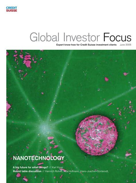
Cover: A droplet of water on a nasturtium leaf doesn’t wet its surface. Instead, it acts as a dust collector, automatically cleaning the surface as it slides off.<br />
Source: University of Basel/Microscopy Center
GLOBAL INVESTOR FOCUS<br />
<strong>Nanotechnology</strong>—08<br />
Bigger isn’t always better. // Billions of dollars are invested in nanotechnology<br />
research each year by companies and governments worldwide to substantiate this claim.<br />
Today, the “technology of the tiny” is still in its embryonic phase, but it harnesses<br />
huge potential. The benefits of this budding science are already apparent in the fields<br />
of healthcare, materials, information technology and many more.<br />
Karl Knop ⁄ nanotechnology expert, i4u GmbH ⁄ ⁄ Editor: Michèle Luderer ⁄ Credit Suisse Publications<br />
<strong>Nanotechnology</strong>: A big future<br />
for small things<br />
<strong>Nanotechnology</strong>, a science that deals with objects with the size of<br />
a few nanometers, is a field that promises astonishing advances in<br />
every facet of society, from computers, to healthcare, to the environment.<br />
Today, nanoscience has added more bounce to tennis balls,<br />
made sunscreen lotions easier to smooth on, and even made trousers<br />
stain-resistant. The first successes, however mundane, are<br />
expected to pave the way for more momentous developments, such<br />
as computers based on fundamentally new physical principles, allowing<br />
simulations of complex systems such as the human brain. Once<br />
the technology to build things from the atom up exists, scientists<br />
should be in a better position to imitate efficient mechanisms existing<br />
in nature.<br />
These scientific breakthroughs might seem far-fetched, but<br />
experts estimate that the move from laboratory demonstrations and<br />
computer simulations to reality will be made within the next 10 to 30<br />
years. This rapid development is made possible as a result of the huge<br />
sums invested into the early stages of research and development by<br />
governments around the world. The United States, for example,<br />
invested approximately 1 billion dollars in nanotechnology research<br />
and development in 2004 alone. That is double the amount invested<br />
in 2001, when former President Bill Clinton launched the National<br />
<strong>Nanotechnology</strong> Initiative (NNI). The United States is not the only<br />
country to recognize the economic and societal potential of nanotechnology.<br />
Never in history before has there been such a unique global<br />
effort in one common theme of research. According to the NNI,<br />
worldwide government funding has increased to about five times what<br />
it was in 1997, exceeding 2 billion dollars in 2002. Asian countries,<br />
including Japan, China and Korea, as well as several European countries,<br />
have made leadership in nanotechnology national priorities. At<br />
25 million dollars a year, Switzerland’s investment per capita is high<br />
by international standards. These governments are digging deep into<br />
their coffers now, because they are aware of the potential substantial<br />
returns. The U.S. National Science Foundation has predicted that the<br />
market for nanotechnology, or products containing nanotechnology,<br />
will reach 1 trillion dollars in 10 to 15 years. That also translates into<br />
an estimated 7 million jobs that will be needed to support nanotechnology<br />
industries worldwide, according to the U.S. National Science<br />
Foundation. >
GLOBAL INVESTOR FOCUS<br />
<strong>Nanotechnology</strong>—09<br />
<strong>Nanotechnology</strong> offers the possibility to analyze, manipulate and modify materials at the atomic level and atom by atom. This is a new quality in<br />
materials engineering with unprecedented potential. / Source: University of Basel – Physics
GLOBAL INVESTOR FOCUS<br />
<strong>Nanotechnology</strong>—10<br />
Super storage from IBM Zurich<br />
Research Laboratory<br />
These days, it’s possible to download<br />
just about anything from<br />
music to pictures, to games and<br />
programs on mobile devices,<br />
such as cell phones and personal<br />
digital assistants (PDAs). These<br />
data take up quite a bit of storage<br />
and manufacturers are working to<br />
keep up with demands for<br />
increased capacity demands. As<br />
current storage technologies are<br />
gradually approaching fundamental<br />
limits, IBM explored innovative<br />
solutions for data storage in a<br />
system called “millipede.” Using<br />
nanotechnology, scientists at the<br />
IBM Zurich Research Laboratory,<br />
Switzerland, have made it to the<br />
millionths of a millimeter range,<br />
achieving data storage densities<br />
of more than one terabit (1,000<br />
gigabits) per square inch. This is<br />
equivalent to storing the content<br />
of 25 DVDs on an area the size of<br />
a postage stamp.<br />
www.zurich.ibm.com<br />
Source: IBM Zurich Research Laboratory<br />
Stain-resistant fabrics<br />
from Schoeller<br />
Schoeller has been working in<br />
nano research and development<br />
since 1998. Using the technology,<br />
it has created textiles with special<br />
properties for stain protection<br />
and oil and water repellence. Fabrics<br />
finished with NanoSphere<br />
provide protection from stains of<br />
all kinds: Even cola, ketchup and<br />
coffee can easily be rinsed off<br />
with a little water. Thanks to nanotechnology<br />
the textile surfaces<br />
are not only easy to clean, they<br />
are robust, long-lasting and can<br />
be laundered less often and at<br />
lower temperatures. The Nano-<br />
Sphere finish is suitable for many<br />
textile applications, including<br />
outdoor, leisure and sports clothing,<br />
business suits, protective<br />
work gear, home furnishing and<br />
medical applications. Clothing<br />
manufacturers around the world,<br />
including Daniel Hechter,<br />
Mammut, The North Face, and<br />
Polo Ralph Lauren, are using<br />
NanoSphere textiles in their production.<br />
www.schoeller-textiles.com<br />
Source: Schoeller Textil AG<br />
Evolution or industrial revolution?<br />
<strong>Nanotechnology</strong>, with its promise of making systems that are smaller,<br />
faster, stronger, better and cheaper to produce, may soon be the<br />
cornerstone of every manufacturing industry.<br />
Most industries that depend critically on materials have already<br />
recognized the importance of nanotechnology for their business. The<br />
microelectronics industry is among them. The industry, which has a<br />
50-year history of making things smaller while preserving and improving<br />
their functionality, believes that breakthroughs in nanotechnology<br />
are needed for its continued growth. In 1965, computer-processing<br />
power consisted of a microchip with 30 transistors. Today, chips have<br />
40 million transistors ranging in size from 130 to 180 nanometers. By<br />
2016, the Consortium of International Semiconductor Companies<br />
expects chips to be radically scaled down and to hold billions of<br />
transistors with the size of only 10 to 20 nanometers. What does this<br />
mean for consumers? We will benefit from faster computers with<br />
larger storage capacities.<br />
While the application of nanotechnology to improve existing<br />
products has a short history, spanning just two decades, it is gaining<br />
momentum rapidly. Nanoparticles have been produced in large quantities<br />
for a long time by making materials smaller and smaller from<br />
large-scale structures into nanometer-scale structures (the so-called<br />
“top-down approach”). The process of creating things by downsizing<br />
into the micrometer scale is called microtechnology. The top-down<br />
approach came as an evolution of microtechnology.<br />
Making things smaller while preserving their functionality is<br />
advantageous. However, this is not the main reason that explains the<br />
potential of nanotechnology. The attractiveness of small particles at<br />
nanometer scale is that they behave very differently from the objects<br />
in our macroscopic world. The reason for that is very fundamental<br />
and is related to quantum phenomena that explain the behavior of<br />
atoms and molecules. Particles at nanometer dimensions behave like<br />
waves, exhibiting “strange” resonances and interacting with other<br />
particles by exchanging well-defined portions of energy called quantums.<br />
While common objects from our daily life must be permanently<br />
fed with energy to be able to move, very small objects may stay<br />
in a steady state of motion without losing energy over a long period<br />
of time. Now, new advances in nanotechnology (bottom-up approach)<br />
add to the “old” top-down approach much deeper understanding and<br />
predictability.<br />
A whole range of start-up companies are developing and selling<br />
novel products used in a wide variety of applications and markets,<br />
ranging from ultra-high precision robots and novel photovoltaic cells<br />
that harness solar energy, to flexible displays, and chip-based medical<br />
sensors. <strong>Nanotechnology</strong> is not the only key technology of the<br />
twenty-first century, but due to its inherent multidisciplinary nature,
GLOBAL INVESTOR FOCUS<br />
<strong>Nanotechnology</strong>—11<br />
There are two different approaches in nanotechnology:<br />
the “top-down” approach, which means downsizing materials from<br />
a larger scale to the nanometer size, and the “bottom-up”<br />
approach, which refers to building nanostructures atom by atom<br />
or molecule by molecule.<br />
it certainly is laying solid groundwork for solutions to many of the<br />
urgent questions of the industrialized world.<br />
p Electronics and information technology: The development of electronics<br />
and information processing has reached a critical point. The<br />
chips used today combine hundreds of millions of interlinked elements<br />
in one chip, however, the miniaturization process has reached<br />
a point where further developments seem not to be possible without<br />
a new and different approach. <strong>Nanotechnology</strong> should provide the<br />
next leap to make further miniaturization possible. Scientists demonstrated<br />
that new significant advancements could be made using the<br />
knowledge provided by nanotechnology, including totally new concepts<br />
for computing based on quantum devices.<br />
p Life sciences: To support and improve human health on a global<br />
scale represents a challenge for the present and near future. Better<br />
insight and control of processes in the molecular scale are needed<br />
for this task. Traditionally, this task has been the domain of biochemistry<br />
and the pharmaceuticals industry. With the advent of nanotechnology,<br />
totally new approaches to manipulate, modify and eventually<br />
design and fabricate molecular structures in the atomic scale are<br />
available today and may ultimately change the whole discipline in the<br />
long term. Biochemical sensors based on nanodevices have already<br />
started to revolutionize medical diagnostics. The real impact of nanotechnology<br />
in life sciences, however, will be far more fundamental,<br />
introducing completely new methods for influencing and altering the<br />
basic processes of life. The areas of medicine and pharmaceuticals<br />
may not be the same again after nanotechnology has entered the<br />
field. The potential of applying this technology to medicine is huge.<br />
Many applications, from drug delivery to advanced diagnostics, are<br />
currently being researched. In the next five years, researches expect<br />
to make headway in drug delivery and advanced diagnostics. For<br />
example, introducing nanoparticles in medicines might make them<br />
more soluble and easier to absorb. Or implanting chips that would<br />
monitor the level of biochemicals in the bloodstream and release the<br />
appropriate level of medication, which would greatly benefit insulindependent<br />
diabetics.<br />
p Energy and new materials: The generation of mechanical energy<br />
strongly depends on the availability of suitable materials. Steel was<br />
virtually the only choice in the nineteenth century. Much stronger and<br />
lighter materials have been developed since then and used to increase<br />
efficiency. Many of these new materials owe their outstanding properties<br />
to their nanoscale crystalline structure. While in the past,<br />
material processing was based on trial and error, nanotechnology is<br />
now offering a well-controlled approach. More recently, new materials<br />
have been discovered, including carbon nanotubes (CNT), which<br />
exhibit a mechanical strength that is 20 times that of steel and just<br />
one-sixth the weight. This will enable the construction of cars ><br />
Mercedes-Benz scratchresistant<br />
cars<br />
DaimlerChrysler has developed a<br />
nanoparticle clear coat for its<br />
car lacquer that is highly resistant<br />
to scratching. It contains microscopic<br />
ceramic particles that form<br />
a densely cross-linked network<br />
when it hardens, providing a<br />
threefold improvement in scratch<br />
resistance. The effectiveness of<br />
the technology was demonstrated<br />
by the results of an extreme<br />
test conducted in an external laboratory.<br />
In long-term studies<br />
involving more than 150 test cars,<br />
the coating proved glossier<br />
and more scratch-resistant than<br />
conventional paint jobs, even<br />
after years of use. After ten wash<br />
cycles with a mixture of water and<br />
fine particulate matter – reproducing<br />
the wear-and-tear effect of<br />
some 50 to 100 regular car<br />
washes – the nano-painted sheet<br />
metal emerged with approximately<br />
40 percent greater gloss<br />
than samples with conventional<br />
lacquer.<br />
www.daimlerchrysler.com<br />
Source: DaimlerChrysler<br />
<strong>Nanotechnology</strong> in a nutshell<br />
p The prefix, nano, comes<br />
from the Greek “nanos,” which<br />
means dwarf.<br />
p <strong>Nanotechnology</strong> concerns materials<br />
and working devices<br />
that are engineered at the scale<br />
of atoms and molecules.<br />
p Atomic constructs can be measured<br />
in nanometers, which are<br />
one millionth of a millimeter in size.<br />
p Approximately 3 to 6 atoms<br />
can fit inside of a nanometer,<br />
depending on the atom.<br />
p A human hair is about<br />
80,000 nanometers wide.<br />
p Proteins, the building blocks of<br />
living organisms, are typically several<br />
nanometers in size.<br />
p Viruses, which are the smallest<br />
living organisms, can reach up<br />
to 100 nanometers, whereas bacteria,<br />
which do not qualify as<br />
nano-objects, are up to several<br />
thousand nanometers in size.
GLOBAL INVESTOR FOCUS<br />
<strong>Nanotechnology</strong>—12<br />
Spheres of polystyrene: Tiny spheres of polystyrene, only a few micrometers in size, may build up in a self-organized manner to form layers,<br />
one above the other, exhibiting extraordinary optical properties, eventually providing trully three-dimensional bulk materials. / Source: CSEM, Inc.<br />
Nature demonstrated this long ago: Colorful opal gemstones are the result of a self-organized<br />
depositing of microscopic particles.
GLOBAL INVESTOR FOCUS<br />
<strong>Nanotechnology</strong>—13<br />
Vertical Cavity Surface Emitting Laser (VCSEL): Semiconductor lasers are omnipresent in modern society. CD and DVD devices<br />
and many other well-established products depend on them. Such lasers contain nanostructures and their evolution will be strongly influenced<br />
by nanotechnology. / Source: Avalon Photonics Ltd.<br />
DVD and CD players are a commodity today. A tiny spot of light from a semiconductor laser<br />
is used to write and read the information on the disc.
GLOBAL INVESTOR FOCUS<br />
<strong>Nanotechnology</strong>—14<br />
Microbes: The growth of microbes strongly depends on the surface. By offering suitable topographies their presence or absence may be<br />
controlled. / Source: CSEM, Inc.<br />
Hip, knee and dental implants are routinely used today to improve the quality of life,<br />
particularly for elderly people. The critical part in these devices is the interface<br />
to the body. Proper surface treatment improves the fixation and may greatly enhance the<br />
lifetime of the implant.
GLOBAL INVESTOR FOCUS<br />
<strong>Nanotechnology</strong>—15<br />
“The impact of nanotechnology on the health, wealth,<br />
and lives of people will be at least the equivalent of the combined<br />
influences of microelectronics, medical imaging, computeraided<br />
engineering and man-made polymers developed in this<br />
century.” // Richard E. Smalley, 1996 Chemistry Nobel Laureate<br />
with a tenfold reduced power consumption and eventually even an<br />
elevator to space, as recently studied by NASA. <strong>Nanotechnology</strong> will<br />
also have potentially significant impacts on energy efficiency, storage<br />
and production. <strong>Nanotechnology</strong> could help revolutionize the energy<br />
industry, producing advances in solar power cell technology and the<br />
development of fuel cells.<br />
No nanotechnology without the right tools<br />
In 1981, Heinrich Rohrer and Gerd Binnig at IBM Research Laboratory<br />
in Zurich developed the scanning tunneling microscope, STM, a device<br />
that enables researchers to analyze and manipulate matter at the<br />
atomic scale. This invention laid the groundwork for further advances<br />
in nanotechnology. Further progression in nanotechnology generated<br />
a demand for new commercial instruments for routine use in the handling<br />
of nanostructures and nanodevices. A whole range of tools<br />
similar to the STM, such as the Atomic Force Microscope (AFM), and<br />
an entirely new generation of instruments has evolved to support microand<br />
nanotechnology. The emerging market of tools for nanotechnology<br />
will play a key role in the development of this industry.<br />
Do the benefits outweigh potential risks?<br />
While many believe that the influence of nanotechnology will be a<br />
universal cure-all, others have serious concerns about its social,<br />
political and economic effects. A primary fear is the use of nanotechnology<br />
will generate unwanted side effects, which could harm lives<br />
and the environment. It is impossible to avoid such effects completely,<br />
as almost any technology can be abused. However, internal<br />
control of scientific and technological developments in nanotechnology<br />
is inherently better than in other fields of high technology. This<br />
is due to the fact that an interdisciplinary group of scientists and<br />
engineers are ultimately responsible for their findings. Nevertheless,<br />
experts predict that governments may soon step in to create laws or<br />
regulations concerning nanotechnology.<br />
æ<br />
Miele’s easy clean ovens<br />
Oven cleaning is not a favorite<br />
chore for most people.<br />
It often gets put off until the task<br />
takes hours of scrubbing to<br />
remove burned-on grease. Knowing<br />
this, Miele has created<br />
PerfectClean enamel, a material<br />
treated with nanotechnology<br />
surface finishing that prevents<br />
food and grease particles<br />
from bonding with the oven cavity,<br />
racks and even its baking<br />
sheets. Spills also can’t burn on.<br />
This technology hasn’t abolished<br />
the need for oven cleaning,<br />
but made it significantly simpler.<br />
www.miele.de<br />
Source: Miele<br />
Hartchrom’s surface technology<br />
Hartchrom, Switzerland, and<br />
Nanogate Coating Systems,<br />
Germany, developed Nanochrome ® ,<br />
a surface technology that is<br />
antiadhesive, and corrosion- and<br />
temperature-resistant. The<br />
Nanochrome ® coating system has<br />
been used for web offset printing,<br />
and resulted in a reduction of<br />
cleaning effort for the paper guide<br />
rolls up to 85 percent. In comparison,<br />
customary paper guide<br />
rolls must be cleaned after<br />
333,000 rotations and Nanochrome<br />
® rolls require cleaning<br />
after only 850,000 to 1.3 million<br />
rotations. Nanochrome ® applications<br />
in other industrial fields,<br />
such as in paper and foil manufacturing,<br />
are being developed.<br />
www.hartchrom.com<br />
Table 1<br />
Estimated public funding of nanoscience<br />
and nanotechnology<br />
Source: Bundesministerium für Bildung und Forschung<br />
(in CHF million) 2000 2001 2002 2003 2004<br />
Europe 240 400 580 850 900<br />
Switzerland 20 25 25 27 30<br />
USA 360 500 680 920 1020<br />
Japan 330 720 900 950 950<br />
Others 180 250 540 600 650<br />
Source: Hartchrom, Switzerland
GLOBAL INVESTOR FOCUS<br />
<strong>Nanotechnology</strong>—16<br />
Expert discussion // <strong>Nanotechnology</strong> has been touted as the panacea for many<br />
of the world’s ailments, but what are its real capabilities? How much of what has been<br />
reported in the popular press is speculation, and how many breakthroughs are<br />
really just around the corner? Four leading experts in the field joined a question and<br />
answer forum to help us weed the facts from the fiction.<br />
Editor: Michèle Luderer ⁄ Credit Suisse Publications<br />
The following discussion was moderated by Arthur Vayloyan, Member of the Credit Suisse Executive Board, Head of Private Banking<br />
Switzerland, and Maria Custer, biochemist, Credit Suisse Equity Research<br />
Unraveling the big debate over<br />
small science<br />
Arthur Vayloyan: Media articles have written that science has<br />
the potential to eradicate air and water pollution, eliminate viruses<br />
and disease, abolish famine and drought, create artificial intelligence,<br />
mimic the processes of life, and much more! Is this fiction or<br />
fact?<br />
Heinrich Rohrer: That is neither fiction nor fact. To date, I have<br />
not heard such claims from respectable scientists engaged in nanotech.<br />
That is part of the hype perpetuated by the media. Nanotech<br />
will provide new solutions that will substantially improve, but not<br />
eradicate these problem areas. For example, considerably reduced<br />
friction will significantly reduce wear and save energy, but some<br />
problems will remain.<br />
Viola Vogel: Engineering materials and devices at the nanoscale<br />
will enable us to do far more with far less resources. This is the driving<br />
force behind miniaturization, as exemplified by various technology<br />
developments over the last decades. By entering the nanoscale,<br />
we might find new solutions to old problems, but we will certainly not<br />
find magical cures.<br />
Hans-Joachim Güntherodt: These examples are a collection<br />
of unrealistic hopes. Today, we are still in the state of nanoscience,<br />
which can also be defined as the beginning or early stage of nanotechnology.<br />
Nanoscience, with its supportive nature, promulgates<br />
throughout all of the scientific disciplines. As a result, it will stimulate<br />
and create new technologies in an interdisciplinary fashion in all of<br />
these fields. This will greatly impact many industrial branches to the<br />
benefit of our everyday lives, but as the others have said, it certainly<br />
will not solve all the problems of our world.<br />
Maria Custer: How is the public to distinguish between fantasy<br />
and reality? Particularly when the popular press prints inaccuracies on<br />
the topic, and science-fiction thrillers, which disparage the technology,<br />
make the bestseller’s lists?<br />
Heinrich Rohrer: Science fiction is as old as science. In fact,<br />
some of what was once considered science fiction has become reality<br />
sooner than ever anticipated. Scientists, however, can lose their<br />
credibility not just by making empty promises, but also with hasty
GLOBAL INVESTOR FOCUS<br />
<strong>Nanotechnology</strong>—17<br />
Heinrich Rohrer, Nobel Laureate: “Nanotech should not copy nature, but<br />
should get inspired by it.”<br />
Hans-Joachim Güntherodt, Director of the National Center of<br />
Competence in Research (NCCR), Switzerland: “Switzerland is well positioned<br />
in this emerging field.”<br />
rejections. So it is best to let science fiction be and to speak up only<br />
if science has been discredited. Science has more important things<br />
to do than crusade against fiction writers.<br />
Viola Vogel: We scientists have to play a far more active role to<br />
help society discriminate between science and fiction.<br />
Hans-Joachim Güntherodt: The responsible sources do have<br />
an obligation to inform and educate the public and to provide them<br />
with scientific and experimental facts.<br />
Maria Custer: In my opinion, experts in biotechnology and<br />
genetics were too late vin explaining to the public what they are doing<br />
in their labs. This led to uncertainty and inacceptance of everything<br />
genetically modified. What responsibility do nanotech experts have<br />
to clear up the confusion?<br />
Viola Vogel: Recognizing this dilemma, the United States initiated<br />
extensive discussions about potential societal and ethical<br />
implications at the onset and as part of the US National <strong>Nanotechnology</strong><br />
Initiative. A discussion about the societal implications of<br />
nanotechnology has to be conducted in the framework of international<br />
economic, medical and environmental challenges. The truth is<br />
that with the rapidly increasing world population, the worldwide<br />
competition for resources will become fiercer. Better technologies<br />
are needed to use our limited resources more efficiently and in better<br />
harmony with the environment. Furthermore, current technologies<br />
are not sufficient to stop or reverse the cost explosion in the<br />
healthcare sector, which might lead to the possibility that patients<br />
do not get the care they deserve. New solutions need to be found,<br />
and accordingly we have to invest into new science and technology.<br />
The public needs to be informed about how, and in what ways, the<br />
emerging new technologies might contribute to the benefit of mankind.<br />
At the same time, we have to start asking early about possible<br />
unanticipated, negative consequences, and how these new technologies<br />
might be purposely misused. Since so many disciplines are<br />
meeting at the nanoscale, a differentiated approach involving many<br />
sectors of society is needed.<br />
Hans-Joachim Güntherodt: The main concern is about the<br />
toxicity of nanoparticles. However, nanoparticle research is only a<br />
segment of the entire field of nanoscience. Regardless, there is no<br />
doubt that we can learn from biotechnology and genetics, how to<br />
interact with the public and let them know what we are doing.<br />
Arthur Vayloyan: Can parallels be drawn between the trend in<br />
nanotechnology and past trends in other research-intensive or highgrowth<br />
disciplines, such as biotech or information technology (IT)?<br />
Rita Hofmann: I believe there are parallels. Biotech and IT<br />
describe a wide variety of industries and applications, some of them<br />
winners and some losers. There are also parallels in the promises<br />
that are made.<br />
For example, when the laser was invented, it was said that it would<br />
change the world. It is now very widely used in telecommunications,<br />
material science physical measures, and in limited medical applications,<br />
but has fully failed in the general medical and chemical industries and<br />
many manufacturing industries. Nanoapplications will fill particular<br />
gaps, but they are not the solution to all of today’s problems.<br />
Viola Vogel: There are many parallels; however, none of the<br />
above technologies involve as many disciplines as nanotechnology.<br />
The exploration of the nanoworld is an endless resource of scientific<br />
discovery, from the physical sciences to engineering, from chemistry<br />
to biomedicine.<br />
This includes the discovery of new physical phenomena and<br />
quantum effects at the nanoscale, watching and probing the properties<br />
of single atoms and molecules, exploring how nature engineers<br />
its materials at the nanoscale, and how biological nanosystems work.<br />
Concurrently, the nanotech community is asking how to either convert<br />
these new discoveries into new technologies, or innovate already<br />
existing technologies. >
GLOBAL INVESTOR FOCUS<br />
<strong>Nanotechnology</strong>—18<br />
Arthur Vayloyan: The nanotech vision includes revolutionizing<br />
industries, such as health and medicine, chemicals, power and energy,<br />
transportation, electronics, agriculture, engineering and defense.<br />
Is the nanotech market going to explode?<br />
Hans-Joachim Güntherodt : If we remember how the transition<br />
from radio tubes to transistors or integrated circuits took<br />
place, what seems to be a revolution today, was evolutionary at<br />
the beginning. Fifty years ago, when the first steps were being<br />
taken with transistors, no one predicted today’s use in laptops,<br />
mobile phones or the Internet. Similar developments have to be<br />
considered for nanotech.<br />
Heinrich Rohrer: Nanotech is a term for a wide variety of processes,<br />
products, and solutions. Its ultimate goal is to perform electrical,<br />
mechanical, chemical, and thermal sensing, processing, and actuation<br />
with systems working on the nanometer scale. It will provide<br />
pervasive bridges between the virtual world of today’s pervasive data<br />
processing and the real world of action. An important aspect is also<br />
new materials with special properties due to distinct nanostructures.<br />
Therefore, it is not one technology, industry, or market – it embraces<br />
many. The transition will be evolutionary, and revolutionary. Just remember,<br />
it took 17 years to replace half of the radio tubes by transistors – an<br />
evolutionary transition. Microelectronics, however, brought the hightech<br />
revolution. Nanotech is neither about “filling particular gaps,” nor<br />
“the solution to all of today’s problems”; it is about the vast world in<br />
between. And, it will revolutionize many branches of industry and, even<br />
more importantly, create new ones.<br />
Arthur Vayloyan : In 2000, the US National Science Foundation<br />
published a report stating that market expectations could reach USD 1<br />
trillion by 2015. What is your opinion on these projections?<br />
Rita Hofmann: It depends what is counted as the market. I would<br />
feel more comfortable with an estimate of 1 percent of goods in world<br />
trade to be related to nanotechnology.<br />
Hans-Joachim Güntherodt: It is too early to make statements<br />
on market expectations in the range of these high volumes. However,<br />
there are sufficient expectations that Swiss spin-offs, start-ups, and<br />
other companies will become interested in the field.<br />
Arthur Vayloyan: Will some trillion-dollar industries be made obsolete,<br />
or will the transition to nanotechnology be smooth?<br />
Rita Hofmann: Many big industries have their own nano programs.<br />
They will probably integrate this new technology into their current structures.<br />
Hans-Joachim Güntherodt: I believe the transition will be smooth<br />
and has to follow commercial laws. We can learn from the introduction<br />
of new technologies in the past. Well-established manufacturers of<br />
radio tubes focused on other businesses or else were made obsolete.<br />
Intel is now the new giant in this field.<br />
Heinrich Rohrer: Obsolete? Hardly. Let’s take the electron microscope<br />
as an example on a smaller scale. It boosted research, development,<br />
and the market of the then 300-year-old optical microscopy<br />
industry. On a larger scale, the power necessary to perform a calculation<br />
decreased by a trillion times over the past five decades, yet<br />
the electricity bill for computers and peripheries increased to about<br />
USD 1 trillion per year.<br />
Going from the microscale to the nanoscale is a natural continuation<br />
of miniaturization. For example, a tera-bit in a cell phone will open<br />
new opportunities for this market, rather than make the cell phone<br />
market obsolete. Adding nanochemical analyzers and synthesizers to<br />
transmit fragrance and scent in addition to words, pictures and whatever<br />
should boost the cell phone market even more.<br />
Other developments, however, might discontinue because many<br />
properties and functions change at the transition from condensed<br />
matter behavior to atomic and molecular properties. A change from<br />
solid state to molecular components will require novel processes and<br />
technologies and, therefore, a lot of courage by the industries involved.<br />
But, it will open new horizons.
GLOBAL INVESTOR FOCUS<br />
<strong>Nanotechnology</strong>—19<br />
Rita Hofmann, Head of Research and Development, Ilford Group,<br />
Switzerland: “Nanoapplications will fill particular gaps, but they are not the<br />
solution to all of today’s problems.”<br />
Viola Vogel, Head of the Laboratory for Biologically Oriented Materials at the<br />
Swiss Federal Institute of Technology, ETH: “We scientists have to play a<br />
far more active role to help society discriminate between science and fiction.”<br />
Maria Custer: What does the change “from solid state to molecular<br />
components” mean? Are there examples?<br />
Hans-Joachim Güntherodt: In the past, we observed the<br />
change from vacuum or radio tubes to transistors, later the field of<br />
solid-state integrated circuits was introduced. Today, lower dimensions<br />
in the micrometer range are state-of-the-art. Smaller dimensions<br />
are not accessible by lithographic processes or limited by<br />
physical laws. Therefore, in the future transistors might be replaced<br />
by molecular components.<br />
Heinrich Rohrer: Molecules are the smallest, nanometer-sized<br />
functional components. One objective of macromolecular chemistry<br />
is to synthesize molecules of increasingly complex functionality. In<br />
many nanotech applications, the electron or ion currents become so<br />
small that we have to count electrons and ions instead of measuring<br />
currents. Using molecules as counting components seems to be a<br />
natural approach, as nature uses them abundantly, for example, molecules<br />
as adjustable holes for transfer of single ions through cell<br />
walls. Dreaming of the distant future, molecules are envisaged to<br />
serve as basic building blocks for self-assembling increasingly complex<br />
functional units and systems.<br />
Arthur Vayloyan: Will large, well-established companies control<br />
the market or is there room for smaller companies and start-ups?<br />
Rita Hofmann: There is a market now for start-ups, primarily<br />
in the equipment and medical sector, and in cases where investments<br />
in very expensive equipment are not needed. However, most<br />
of the activity will be in traditional industries and with big industrial<br />
players that invest in nanotechnology. For example, digital manufacturing<br />
and manufacturing-on-demand use manipulation on a fine<br />
scale. It is my guess that every major chemical company, every<br />
electronics company and many manufacturing industries have nanotechnology<br />
programs. There are also start-up groups in traditional<br />
industry.<br />
Heinrich Rohrer: There are opportunities for new companies,<br />
and they will appear. Just look at the developments in the data processing<br />
industry since 1960, thanks to microelectronics.<br />
Hans-Joachim Güntherodt: Today, there are examples of<br />
activities for both alternatives. Several well-established companies,<br />
such as IBM, Hewlett-Packard, and Hitachi, hold patents. Some startups<br />
are also already making profits. The start-ups in the field of scanning<br />
probe microscopy can all be linked to universities working in this<br />
field. Therefore, it is hard to speculate on who will control the market.<br />
Arthur Vayloyan: What are your views on nanotech programs<br />
in large companies compared with small start-ups coming from the<br />
academia?<br />
Rita Hofmann: Start-ups have the disadvantage of having to<br />
develop new products for markets that might not yet exist to assure<br />
their living. For example, commercializing a new industrial product in<br />
my industry can cost anywhere from CHF 4 million to 10 million. This<br />
covers only technical development, not investing in any infrastructure<br />
or manufacturing equipment for longer-term sustainability. If startups<br />
have this kind of money available to them, they have a chance.<br />
Start-up groups in large companies do not have access to external<br />
funding.<br />
Viola Vogel: Not all products derived from nanotechnology are<br />
targeting new markets. Many start-up companies in the US are targeting<br />
existing markets with new products.<br />
Hans-Joachim Güntherodt: I believe the topic of start-ups is<br />
linked to the academic environment. In large companies, the programs<br />
are much more focused on the extension of existing products<br />
towards the advantages of the nanoscale.<br />
Maria Custer: So, the expectation is that larger companies will<br />
be the first to successfully introduce nanotech products, and smaller<br />
companies with great ideas will most likely need to collaborate >
GLOBAL INVESTOR FOCUS <strong>Nanotechnology</strong>—20<br />
with larger institutions in order to get access to the needed infrastructure,<br />
funding and marketing expertise?<br />
Rita Hofmann: That would be a good approach. For high-tech<br />
industrial products, the funding requirements are very high (investment<br />
in safety, manufacturing equipment, research, marketing, etc.).<br />
This is a heavy burden for start-ups and for existing small enterprises.<br />
Collaboration among companies is a good solution.<br />
Hans-Joachim Güntherodt: There are spin-offs, for example,<br />
that have successfully introduced nanotech products in the field of<br />
new microscopes. They are making money and do not need venture<br />
capital. In the chemical industry, larger companies are also realizing<br />
good profits with nanotech products.<br />
Viola Vogel: If we can learn from the very recent past, start-up<br />
companies can have a very competitive edge. Start-up companies,<br />
for example, drove technical innovations in biotechnology and IT, in<br />
a major way. Some of these companies grew rapidly and larger companies<br />
bought others up. This was and is the case at least in the US.<br />
The overhead of a big company to develop new technologies and<br />
prototypes is typically higher than for start-up companies. Unless the<br />
product requires expensive nanofabrication technologies, start-up<br />
companies can afford the expenses of developing new prototypes<br />
and products. Many of the nanoproducts that are coming to the<br />
market today rely on cheaper manufacturing processes, including the<br />
assembly of specially designed nanoparticles or molecules.<br />
In order to create an environment in which nanotech start-up<br />
companies can flourish, they must have access to centralized user<br />
facilities where they can either analyze the structure and properties<br />
of their products, can conduct micro- and nanofabrication processes<br />
if needed, or have access to a well-trained workforce. The<br />
US government invests heavily across the country in such centralized<br />
nanotech facilities that are accessible to academic and industrial<br />
users. Most of those user facilities are housed in academic institutions<br />
or national laboratories. Furthermore, the regions from which<br />
the major new biotechnology and IT industries have emerged are<br />
found in close proximity to prime universities. Investments into prime<br />
university-based research programs serve as major engines for<br />
innovation.<br />
Maria Custer: Do you believe that some really innovative and<br />
life-changing products will be developed? If we take the cell phone as<br />
an example, a few years ago it was not thinkable that almost every<br />
person would need a cell phone. In my view, this changed many people’s<br />
lives because they can be reached all the time and everywhere.<br />
Viola Vogel: Talking about life-changing products: in medical<br />
emergencies, the time delay between taking a patient’s blood sample<br />
and getting back the results from centralized laboratories often<br />
exceeds the remaining life expectancy of the patient. Miniaturization<br />
will soon make it possible to analyze blood and other body fluids on<br />
the spot, for example at the site of an accident or wherever needed<br />
through the use of microfluidic devices that contain integrated nanosensors<br />
and reporters.<br />
Hans-Joachim Güntherodt: There will be a variety of products<br />
coming close to these criteria. It might even be that the mobile phone<br />
will benefit from such a development.<br />
In biology or medicine, the dimensions of life are more easily<br />
accessible in diagnostics and therapy by nanomechanical devices in<br />
development. On the other hand, there is the emerging field of nanotextiles.<br />
Be aware that there might be unexpected developments<br />
which today cannot be foreseen.<br />
Arthur Vayloyan: What regions or countries are in a good position<br />
to benefit from nanotechnology?<br />
Rita Hofmann: Asia is well placed to adopt it, because many<br />
countries are oriented very much towards manufacturing industries,<br />
compared with social sciences and services, for example.<br />
Heinrich Rohrer: Europe is positioned as good as the east and<br />
west. But that is not sufficient. Europe was scientifically leading in
GLOBAL INVESTOR FOCUS<br />
<strong>Nanotechnology</strong>—21<br />
Arthur Vayloyan, member of the Credit Suisse Executive Board and<br />
Head Private Banking Switzerland: “It is one of our primary responsibilities to<br />
provide timely, well-founded advice, identify investment trends and new<br />
markets at an early stage, and to realistically evaluate opportunities and risks.”<br />
Maria Custer, biochemist, Credit Suisse Equity Research: “Although its<br />
potential is difficult to assess, the chances that nanotechnology will change<br />
traditional industries and global economic structures are high.”<br />
the 20th century – and before. However, Europe missed the three<br />
major technology developments: microelectronics or microtechnology<br />
as a whole, computers and informatics, and biotechnology. Let’s<br />
hope for the best this time.<br />
Viola Vogel: In terms of governmental investments in nanotechnology,<br />
Europe, Asia and the US are shoulder to shoulder. The question<br />
will be how well Europe is prepared to convert new discoveries<br />
into competitive products.<br />
Hans-Joachim Güntherodt: Let me focus on Switzerland,<br />
where Heinrich Rohrer and Gerd Binning invented a major ingredient<br />
of nanoscience, the scanning tunneling microscope, in 1981. This<br />
triggered nationwide efforts in the field. Nearly every university and<br />
other academic institutions are working in nanoscience. In the past<br />
few years, the Technology Oriented Program (TOP) NANO 21, which<br />
was created to ensure that Swiss businesses can make rapid use of<br />
nanometer-based technologies, has tried to promote cooperation<br />
between academia and industry. In addition, the Commission for<br />
Technology and Innovation’s nano/micro branch, in collaboration with<br />
the Swiss Academy of Engineering Sciences (SATW), established a<br />
transfer college. The National Center of Competence in Research<br />
“Nanoscale Science” has developed into a center of excellence, and<br />
a nano curriculum has been started at the University of Basel, where<br />
a new type of scientist will be educated. All this might further contribute<br />
to the very good position of Switzerland in this emerging<br />
field.<br />
Arthur Vayloyan: What are the short-, medium-, and long-term<br />
objectives and application areas of nanotechnology?<br />
Viola Vogel: The availability of nanoprobes and instrumentation<br />
to visualize and manipulate biological nanosystems will fundamentally<br />
change our knowledge base in the biosciences, and will contribute<br />
in a major way to transitioning biology from a descriptive to a<br />
quantitative science. Beyond providing new insights into how cells<br />
and organs work, the biggest pay-off for society might come from<br />
utilizing these quantitative insights combined with advanced imaging<br />
and analytical technologies for the early detection of diseases and<br />
their more effective treatment.<br />
Heinrich Rohrer: In the short term, we can expect nanotechnology<br />
to be applied to instrumentation and analytics; imaging and<br />
sensors are examples. Another rapidly growing area deals with nanostructured<br />
materials. In the medium term, it will be applied to molecular<br />
components, novel mechanical and chemical components (such as<br />
holes as gates to count electrons and ions, nanochemistry laboratories<br />
for in-situ synthesis), simple nanosystems (such as Millipede,<br />
a novel type of storage device developed in the IBM Rüschlikon<br />
Laboratory) ; in-situ growth and self-assembly of nanostructures and<br />
simple components; and the study of complex nanoprocesses (such<br />
as systems biology of cells ). In the long term, we might see remote<br />
(wireless) control of autonomous nanosystems and nanorobots, and<br />
self-assembly of whole nanosystems from nanocomponents (living<br />
objects are such self-assemblies; however, they are not subject of<br />
nanotech).<br />
Arthur Vayloyan: Along with the benefits also come potential<br />
and perceived risks. For example, there will certainly be public policy<br />
and social issues, such as safety, health risks, fear of unemployment<br />
(human labor made redundant by machines that produce better<br />
machines ), and moral issues (genetic manipulation ) to be considered.<br />
What are the true negative implications?<br />
Heinrich Rohrer: Today, we should be better prepared than we<br />
were when for example DDT and other pesticides, Freons, and dangerous<br />
chemicals were produced and used. We also recognize that<br />
it is not just a question of “what?” but also of “how much?” The true<br />
negative implication of nanotech is – as with other technical<br />
and social developments – the ever-growing separation of humankind<br />
into those who can keep up with change and those who cannot and,
GLOBAL INVESTOR FOCUS<br />
<strong>Nanotechnology</strong>—22<br />
as a consequence, into those who have and those who have not. That<br />
might eventually end up in a revolution of a different dimension.<br />
Rita Hofmann: At Ilford, we use some nanoparticles in our products.<br />
Our particles are silica, which is an industrial product used in<br />
ketchup, tires and much more. It is known to be chemically very benign<br />
with no special health and safety restrictions. But because they are<br />
nanoparticles we treat our nanosilica as if it was an unknown and<br />
potentially harmful compound. Thus lab personnel and workers wear<br />
protection and open handling is mostly avoided. This is well above any<br />
legal requirements and in line with other potentially dangerous substances<br />
that the chemical industry handles. My point is, there may be<br />
risks, but they can be handled with existing technology. The health<br />
and safety aspects have to be looked at from the beginning.<br />
Viola Vogel: A better scientific understanding needs to be<br />
derived about how nanoparticles might impact human health upon<br />
entry into the human body. The biggest producers of nanoparticles<br />
right now, however, are not the nanotech industries, but combustion<br />
processes.<br />
Hans-Joachim Güntherodt : The true negative implications<br />
might be related to the toxicity of nanoparticles. However, there is<br />
also a challenge to study safety and risk issues and to prevent the<br />
negative impact on human health. At the NCCR “Nanoscale Science,”<br />
we also focus on ethical questions and safety issues. The European<br />
Union Research Program has started a larger study on these topics.<br />
On the other hand, there are always alternatives to handle nanoparticles,<br />
not in the air but in liquids, or to build up nanoparticles for<br />
medicine from peptides, for example. Again, research will be very<br />
helpful.<br />
Arthur Vayloyan: Is it foreseeable that governments might soon<br />
step in to create laws or regulations concerning nanotechnology?<br />
Viola Vogel: Some aspects of nanotechnology can be handled<br />
with existing laws and regulations; others need to be carefully<br />
assessed. The Food and Drug Administration (FDA) in the US, for<br />
example, regulates substances according to their chemical composition<br />
but the agency does not yet consider whether there might be<br />
size-dependencies in their toxicities.<br />
Heinrich Rohrer: I just hope that they don’t overdo it. Any<br />
measures taken should focus first on sound consumer attitudes,<br />
which are worth more than regulations.<br />
Hans-Joachim Güntherodt : This is a far sounder alternative<br />
than a moratorium to stop research in the field of nanoparticles,<br />
which has been suggested by some non-governmental organizations.<br />
Arthur Vayloyan: Is it, however, safe to say that overall benefits<br />
of nanotechnology outweigh the risks?<br />
Heinrich Rohrer: We have to see the benefits outweigh the<br />
risks. There is simply no way around nanotechnology, be it for a<br />
sustainable world or be it for the progress of technology at large.<br />
Viola Vogel : While this will be the case for many or most nanotech-based<br />
products, the scientific communities together with other<br />
sectors of society have to be more alert than in earlier developments<br />
in order to assess potential health risks early in the process.<br />
Hans-Joachim Güntherodt : The future might show that the<br />
risks are under control and can be significantly reduced, and that<br />
nanosciences will undoubtedly benefit mankind.<br />
æ
GLOBAL INVESTOR FOCUS<br />
<strong>Nanotechnology</strong>—23<br />
Where will nanotechnology lead? // <strong>Nanotechnology</strong> might be invisible to the naked<br />
eye, but it is present in many of today’s commercial products. Its effects on our daily<br />
lives so far have been small, but significant. For example, if you are wearing eyeglasses to<br />
read this article, chances are that the lenses are covered with a protective, glare-proof<br />
coating engineered at the nanoscale. In the near future, these minor advances will pave<br />
the way for more life-changing products.<br />
Michèle Luderer ⁄ Credit Suisse Publications<br />
It’s a small, small world<br />
Even though we can’t see it, nanotechnology is in many of the products<br />
we use daily. It can be in our cars, personal computers, clothing,<br />
and even sports equipment. <strong>Nanotechnology</strong> is an enabling technology,<br />
which means that while it appears only in a minute “corner” of a<br />
product, it enhances the product’s functionality, makes it stronger or<br />
increases longevity. Tennis balls are good examples. Thanks to nanoclay<br />
coatings that decrease gas permeability, today’s tennis balls last<br />
five times longer and have more bounce. It has also helped to make<br />
tennis racquets stronger and more lightweight. Are small wonders<br />
such as scratchproof car lacquers and lightweight bumpers with<br />
improved corrosion resistance worth the billions of dollars invested<br />
by governments into nanoscience research? The proponents say<br />
support at this early stage is necessary for nanotechnology to realize<br />
its full future potential.<br />
With nanoscience research underway for more than 20 years, it<br />
is already possible to measure the economic impact of some applications,<br />
according to the United States National <strong>Nanotechnology</strong> Initiative<br />
( NNI), a federal research and development program for nanoscale<br />
science, engineering, and technology. The US Navy, for example, has<br />
been using air-conditioning gears that have a wear-resistant nanoceramic<br />
coating in its ships in 2000. As a result, it expects to have<br />
saved USD 20 million in maintenance costs by 2010. This technology<br />
will likely be used in the car and industrial machinery industry to<br />
extend the lifetime of moving parts. The auto industry is already saving<br />
money by reducing the amount of precious metals used in catalytic<br />
converters by using nanosized platinum particles.<br />
Today’s nanotechnology applications do more than save money,<br />
they also contribute to improved environmental conditions and health.<br />
For instance, products using nanoparticles that can remove bacteria,<br />
viruses, and chemicals from water systems are on the market for use<br />
in large-scale water purification plants, according to the NNI. In the<br />
medical industry, nanocrystals used in biological imaging for diagnostics<br />
make the detection of biological activity in cells much easier,<br />
because they are a thousand times brighter than the conventional<br />
dyes used in tests, such as magnetic resonance imaging.<br />
In the near future, the NNI expects the introduction of advanced<br />
drug-delivery systems, including implantable devices that automatically<br />
administer medications when needed. It also anticipates a reduction<br />
in the use of fossil fuels as a result of the introduction of less<br />
expensive, more efficient solar cells to be used in homes and companies.<br />
What’s in store for the next decade? Experts say that it’s difficult<br />
to predict what products will be on the market, but if medical and<br />
environmental developments continue at this pace, the future looks<br />
bright.<br />
æ
GLOBAL INVESTOR FOCUS<br />
<strong>Nanotechnology</strong>—24<br />
Benefit today: Nanoparticle-enhanced<br />
inkjet photo paper give photo labs a<br />
run for their money<br />
The digital revolution of photography has created a need for a new generation of superabsorbent,<br />
high-quality inkjet paper to keep up with the new photo quality inkjet printers. Traditional<br />
silver-based inkjet paper suffers from slow drying-time and inferior image quality with<br />
respect to resolution. With the introduction of nanoparticles to its high-quality inkjet paper,<br />
Ilford has substantially improved ink absorption. Those problems have been improved sub<br />
stantially and even high-quality transparent coating becomes available. Ilford Switzerland has<br />
recognized this potential of nanotechnology very early and, today, is one of the leading brands<br />
selling nanoparticle-coated photographic inkjet paper of highest quality. / Text: Karl Knop<br />
Photo: Ilford Switzerland
GLOBAL INVESTOR FOCUS<br />
<strong>Nanotechnology</strong>—25<br />
Benefit today: <strong>Nanotechnology</strong> mimics<br />
nature with self-cleaning surface<br />
structures that repel water and dirt<br />
Nature is in the lead when it comes to self-cleaning surfaces. Let’s take the lotus flower as an<br />
example. Its leaves feature a nanostructured surface that repels water. When the droplets roll<br />
off, they pick up small particles of dirt in a self-cleaning process. German botanist Wilhelm<br />
Barthlott first explained this phenomenon known as the lotus flower effect. Today, the first<br />
commercial products such as home and auto paints, roof tiles, window glass, kitchen tools and<br />
other equipment with dust-sensitive surfaces are appearing on the market. Apart from the<br />
gain in maintenance convenience, such products contribute to environmental friendliness as<br />
the use of chemical cleaning agents is reduced. / Text: Karl Knop<br />
Photo: Nanosys GmbH, Switzerland
GLOBAL INVESTOR FOCUS<br />
<strong>Nanotechnology</strong>—26<br />
Benefit today: The future looks brighter<br />
with displays<br />
The generation of light for the past hundred years has been a domain of metals and semiconductors.<br />
Now, soft organic plastic materials have begun to challenge this position, offering<br />
increased performance and brighter light. Organic light-emitting diode (OLED) technology is<br />
composed of several, nanometer-thin layers of polymer materials. They can emit visible light of<br />
any spectral color, are cheaper to produce, have better contrast, use less power and can be<br />
deposited on flexible surfaces. OLED screens are about one-third thinner than today’s liquid<br />
crystal displays (LCD), and don’t need a backlight. Because of their mechanical flexibility, they<br />
can be attached to curved surfaces, such as the robotic finger pictured above, for illumination<br />
purposes. So far, smaller gadgets, such as mobile phones, digital cameras and personal digital<br />
assistants are emitting brighter light thanks to the technology. However, commercial production<br />
of computer monitors and TVs is still on the horizon. / Text: Karl Knop<br />
Photos: CSEM Inc, Switzerland
GLOBAL INVESTOR FOCUS<br />
<strong>Nanotechnology</strong>—27<br />
Benefit tomorrow: More precise and<br />
faster lab results with new diagnostics<br />
tools<br />
In medical diagnostics the traditional biochemical testing of body fluids (blood, urine, etc.) is<br />
a very time-consuming process. At CSEM in Neuchâtel, a revolutionary technology based on<br />
optical waveguides is currently being developed, which is not only extremely sensitive in detecting<br />
specific biomolecules but also relatively easy to use. The whole system consists of a disposable<br />
chip, capable of detecting simultaneously up to nine substances utilizing a small<br />
table-top reader instrument. The new technique is also suited for other application fields such<br />
as food quality testing and environmental control. / Text: Karl Knop<br />
Photo: CSEM Inc, Switzerland
GLOBAL INVESTOR FOCUS<br />
<strong>Nanotechnology</strong>—28<br />
Benefit tomorrow: <strong>Nanotechnology</strong><br />
to shape the fabric of our lives with<br />
smart textiles<br />
Textiles are the most common industrial products, which are – in the true sense – closest to our<br />
bodies. The textile industry is awaiting a revolution by a new class of synthetic fibers and fabrics<br />
with novel functional properties based on micro- and nanotechnologies. These smart textiles will<br />
offer higher comfort to the user, exhibit unusual self-cleaning properties, and might even be<br />
capable of actively adopting to changing environmental conditions, such as temperature, humidity<br />
and air composition. Sensing elements and components to generate electrical energy might also<br />
be integrated to power all these functions. / Text: Karl Knop<br />
Photo: EMPA, Switzerland
GLOBAL INVESTOR FOCUS<br />
<strong>Nanotechnology</strong>—29<br />
Future benefit: <strong>Nanotechnology</strong> will<br />
be integrated into many innovations<br />
that improve our daily lives<br />
Roof covered with<br />
photovoltaic paint<br />
generates electricity to<br />
produce hydrogen fuel<br />
Climate sensors<br />
everywhere<br />
Home cinema with<br />
large self-illuminating screen<br />
based on OLEDs<br />
Self-cleaning and<br />
electrically tunable<br />
transmission windows<br />
Bedside medical center with<br />
elementary diagnostics and<br />
direct link to the doctor<br />
Variable room<br />
illumination<br />
(white, colored)<br />
integrated in<br />
surface structures<br />
Activity-adaptive<br />
smart clothing<br />
Highly scratchresistive,<br />
dustrepellent paint<br />
Solid-state hydrogen<br />
storage and fuel cells<br />
drive electricity<br />
Self-organized food storage<br />
helps keep track of stock<br />
Extrastrong and<br />
extralight materials for<br />
high-efficiency cars<br />
Text: Karl Knop
GLOBAL INVESTOR FOCUS<br />
<strong>Nanotechnology</strong>—30<br />
“Our development inevitably led us to<br />
nanotechnology”<br />
The English company Ilford, a 125-year-old<br />
stalwart, was for decades the undisputed<br />
market leader in the field of monochrome<br />
photographic materials. Then the digital<br />
camera burst onto the scene, triggering the<br />
inexorable decline of traditional photography,<br />
which for Ilford UK culminated in insolvency<br />
one year ago. However, Ilford’s Swiss<br />
arm – Imaging Switzerland GmbH in Marly<br />
near Fribourg – took a new and pioneering<br />
path early on, entering the lucrative and<br />
growing nanotech printing paper business.<br />
Rita Hofmann, Head of Development,<br />
answers our questions.<br />
Rita Hofmann, Ilford Imaging<br />
Daniel Huber // When did you first seriously consider developing<br />
new products in the area of nanotechnology at Ilford Switzerland?<br />
Rita Hofmann: It must have been about eight or nine years ago. If<br />
you want to make the kind of transparent layers we need in the field<br />
of photography, you have to use particles that are way below the<br />
wavelength of visible light, which puts them in the nanometer<br />
realm.<br />
And what makes your high-resolution paper for inkjet printers so<br />
much better than conventional paper?<br />
If you use our paper to print out a digital camera picture, it looks like<br />
and has all the characteristics of a photograph. A layman can barely<br />
tell the difference between these images and a normal photograph.<br />
Do you need a particularly good inkjet printer for the job?<br />
Nowadays, all the standard printers are good enough to deliver the<br />
full photographic quality.<br />
Where did the money come from to develop this innovative paper?<br />
Ilford greatly cut back on research in the traditional photography<br />
field – which was a bit of a risk because, at the time, it was still our<br />
main business. Nevertheless, we switched the bulk of research over<br />
to the new products, which for five years made little contribution to<br />
our business. In fact, for a long time we had no idea whether we’d<br />
ever make money from them.<br />
Why was this R&D work undertaken at Ilford’s Swiss arm?<br />
Because the Swiss development department was already very<br />
advanced in this field. We were never involved over here in Ilford’s<br />
traditional monochrome photographic paper business, we were in<br />
the color segment, the more complex ILFOCHROME branch. Also,<br />
we moved away from traditional analog to digital photography relatively<br />
early on, and ended up concentrating entirely on nonphotographic<br />
hardcopy technologies.<br />
How did the development work go?<br />
From research initially focused on materials that were pretty similar<br />
to traditional photographic layers, we moved on to seeking materials<br />
that would absorb ever more quickly with ever finer particles, which<br />
inevitably led us to nanotechnology. So in that respect we’re no<br />
futuristic developer of nanotech robots and the like, we just use<br />
nanochemistry and nanoparticles.<br />
Why did the Ilford parent company in England miss the new technology<br />
bandwagon?<br />
Within the group, we still had the more advanced and more elaborate<br />
coating technology. Up to the day it closed, the UK site remained<br />
deeply rooted in its traditional photographic paper business and<br />
almost exclusively produced photographic materials, so it lacked the<br />
highly versatile production equipment for elaborate multiple-layer<br />
processes that we have. And to build the facilities at both sites simul-
GLOBAL INVESTOR FOCUS<br />
<strong>Nanotechnology</strong>—31<br />
“We soon knew that it was possible,<br />
but the big problem was implementing it<br />
into production.” // Rita Hofmann<br />
taneously would have entailed heavy investment within a short period.<br />
The group didn’t have that kind of money. Besides, the Swiss site<br />
alone had sufficient capacity to serve the market.<br />
So was it pure luck that, from the outset, you were the more sophisticated<br />
site, almost completely removed from the parent company’s<br />
core business?<br />
Only to a certain extent. My boss was basically responsible for both<br />
sites. To put it simply, he was faced with the following dilemma: say<br />
you have two sports teams, each with their own strengths. What do<br />
you do? Do you try and make them equally strong, or do you make<br />
the better team even better and leave the weaker team to its fate?<br />
He chose the latter, in other words he invested primarily in the site<br />
that was already more advanced. The other site was to follow when<br />
capacity was demanded. That was – and very much is – the advantage<br />
of the Swiss site. From the point of view of long-term success,<br />
he did the right thing. Of course, the money could have been shared,<br />
but then we would never have gained the edge we have today and<br />
certainly wouldn’t be able to work with these materials.<br />
How much of an edge do you have on the competition?<br />
There are a handful of other companies active in this field. But at the<br />
moment we still have the crucial advantage of having a much better<br />
price-performance ratio, better production facilities and greater knowhow.<br />
Of course, this gap can be closed pretty quickly with enough<br />
capital, but right now we’re in a very good position.<br />
When developing a new product, after basic research comes the<br />
development stage and then production. At which stage did you enter<br />
the process at Ilford Switzerland?<br />
Very early on. We even did some of the basic research.<br />
How hard was it then to move into production?<br />
That was the hardest part of all, and took more than four years.<br />
So the huge potential was soon apparent. The question remained<br />
how quickly and how efficiently could you move on to production?<br />
Precisely. It didn’t take us very long to ascertain that we could realize<br />
the product in the laboratory environment. But the major sticking<br />
point was how to put it into production. It’s similar to semiconductor<br />
development: a single semiconductor prototype never took very long<br />
to realize, but the real challenge was to develop a production process<br />
with few rejects and high quality demands in terms of error rate. In<br />
this regard, we have a real edge in know-how.<br />
So then you were able, in principle, to concentrate on developing and<br />
producing special nanotech production machines?<br />
Not many people can afford to spend millions building an entire<br />
machine from scratch. Besides, we’re not mechanical engineers – we<br />
deal with chemistry and paper technology. We could sell individual<br />
processes – but of course we don’t. After all, it is precisely this that<br />
makes us attractive to potential buyers.<br />
How important was Switzerland to you as a location?<br />
It was certainly a factor. People take their work very seriously here and<br />
are well educated at all levels, which is vital. What’s more, as a center<br />
of technology, Switzerland isn’t all that big, which means you still have<br />
that vital personal contact. The research is also of a very high quality;<br />
Switzerland is right up there, particularly in nanotechnology. But not<br />
only does Switzerland have the basic research, it also has the engineering<br />
knowledge to translate that research into a technical product. This<br />
is frequently lacking in other countries, where there’s often a huge<br />
divide between great ideas and industrial reality.<br />
The pioneer days are over, the machines are up and running; now it’s<br />
about making it all pay. Is it gradually getting boring?<br />
No, now it’s time for the next step. Thus far, we’ve only applied this<br />
technology to inkjets, but that has a limited lifespan. There’s no doubt<br />
that the technology won’t last 150 years like photography; 20 to 30<br />
years would be nearer the mark. Now we have to make greater use<br />
of our coating technology for other applications and really push back<br />
the frontiers.<br />
Don’t you first have to recoup all of the investment that was made?<br />
We’ve already written off a lot of the investments; they were part and<br />
parcel of our history in photography. But that’s the price of admission<br />
for others who are just starting out. We benefited from the fact that<br />
a lot was already in place.<br />
So you can really give free rein to progress. Supposing you were<br />
bought by a large conglomerate, aren’t you worried that this momentum<br />
might be slowed down or even lost?<br />
No. Technology is a key factor in our sale. Why should somebody<br />
acquire it if they don’t want to exploit it? In fact, it would actually<br />
benefit us to be part of a larger company. But it would certainly be a<br />
challenge to maintain momentum and focus in a larger corporation.<br />
It’s something we have succeeded in doing in the past, as part of<br />
Ciba-Geigy and International Paper.<br />
Your research has taken you to a largely uncharted microcosm. Is there<br />
any way in which these new discoveries give you cause for alarm?<br />
I don’t buy these science fiction horror stories. As I said before, we’re<br />
not into developing nanotech robots. That said, we do have to handle<br />
our very, very fine particles with care. We always treat new and<br />
unknown substances with the utmost caution.<br />
But otherwise, I’m not really worried about new nanotech developments<br />
being misused for some nefarious end. We foster an open<br />
information policy and dialogue with everyone involved, both within<br />
and outside the company.<br />
æ
GLOBAL INVESTOR FOCUS<br />
<strong>Nanotechnology</strong>—32<br />
Investing in nanotechnology is<br />
its own science<br />
The burgeoning field of nanotechnology<br />
promises huge potential in many sectors<br />
of the economy. Investors who want to<br />
position themselves in this technology<br />
must be able to distinguish between<br />
reality and science fiction.<br />
Maria Custer / Credit Suisse<br />
Figure 1<br />
Performance of quoted stocks with exposure<br />
to nanotechnology<br />
Source: Datastream<br />
260<br />
220<br />
180<br />
140<br />
100<br />
60<br />
20<br />
Price Index<br />
05/02<br />
01/03<br />
Nano Basket Equal WE<br />
NASDAQ Composite<br />
01/04<br />
01/05<br />
Many of the nanotech “visions” that reach the public are just<br />
fantastic ideas without any scientific basis. <strong>Nanotechnology</strong> is a<br />
reality today, and the market for products containing nanotech is<br />
rapidly beginning to emerge. However, due to the heterogeneity<br />
of this science and the broad range of thinkable applications, it<br />
is very difficult to estimate the market potential for nanotechnology<br />
products at this stage. The US National Science Foundation<br />
estimated in 2001 that the nanotechnology market will reach a<br />
size of USD 1 trillion annually by 2015. The difficulty in estimating<br />
the market size begins with the definition of what is nanotechnology<br />
and what is included in the current nanotech market. Several<br />
factors, such as time-to-the-market of nanotech products (the<br />
success of basic products in this area, the success of finding<br />
applications, the time to scale up products), barriers to entry,<br />
penetration rates and global economic growth, play an important<br />
role in the estimates.<br />
Although its potential is difficult to assess, the chances that<br />
nanotechnology will change traditional industries and global economic<br />
structures are high. The better investors understand the<br />
nanotechnology market at its current early stage, the more they<br />
will be able to profit from the expected changes.<br />
Investment case and strategy<br />
Investing in nanotechnology is not easy because the investment<br />
landscape is not yet established. Although the number of companies<br />
with nanotechnology products under development is increasing<br />
significantly, many of these companies are currently at a very<br />
early stage and are privately held, financed by governmental<br />
research funds or venture capitalists. There are a few publicly<br />
quoted nanotechnology companies, but those expected to achieve<br />
the largest part of their revenue and profits with nanotechnology<br />
products have a small market capitalization. This makes it difficult<br />
to build a nanotechnology investment portfolio without including<br />
larger, established companies, and those have only limited exposure<br />
to nanotech. Reflecting this, for the time being, the number<br />
and size of investment vehicles allowing risk diversification, such<br />
as nanotechnology funds, are limited.<br />
In addition, nanotechnology is an interdisciplinary technology<br />
that can be used in many different industries in contrast to traditional<br />
industries like pharma, where investors can obtain exposure<br />
in a single, well-defined part of the stock market.<br />
We have identified the following approaches to invest in nanotechnology:<br />
p Large companies with exposure to nanotechnology (for example:<br />
BASF, Dow Chemical, General Electric, General Motors, Hewlett-<br />
Packard, Intel, IBM, etc.)<br />
p Companies that provide equipment and nanomaterials for<br />
nanotechnology research (for example: Veeco, FEI Company)<br />
p Smaller companies with high exposure to nanotechnology<br />
(for example: Flamel Technologies, Nanogen)<br />
Large companies with exposure to nanotechnology<br />
Many major global corporations with significant research and<br />
development operations are investing heavily in the development<br />
of nanotechnology. This is an effort to keep up with technological
GLOBAL INVESTOR FOCUS<br />
<strong>Nanotechnology</strong>—33<br />
change and to profit from advances in product differentiation and<br />
manufacturing cost reductions. However, these companies are<br />
typically large, well established, profitable, and the nanoinvestments<br />
do not have a material contribution to earnings. As a result,<br />
the returns coming from this technology are low relative to the<br />
total profits achieved from non-nanotechnology products.<br />
Companies that enable nanotechnology research<br />
Another possibility to invest in nanotechnology is through companies<br />
that enable research, development and manufacturing process<br />
by providing the tools and materials needed. For investors<br />
who believe that this technology will play an important role during<br />
the next decade, investing in stocks from companies producing<br />
enabling equipment is a good solution, as this kind of machinery<br />
will be needed not only for the production of innovative products<br />
but also for research and development. This approach implies<br />
higher risks and higher returns from nanotechnology than investing<br />
in established large corporations.<br />
Smaller companies with high exposure to nanotechnology<br />
This third option includes early-stage companies, developing intellectual<br />
property in nanotechnology, and is the riskiest approach.<br />
In our view, it is not possible to pinpoint a particular product under<br />
development that will turn out to be the most successful opportunity<br />
among hundreds of projects that will most likely fail.<br />
However, there are a few companies listed with nanotech<br />
products under development such as Flamel Technologies, a<br />
company focusing on drug delivery. The company developed a<br />
nanocarrier for the delivery of proteins called Medusa ® . Medusa<br />
is a self-assembled polyamino acid nanoparticles system that<br />
allows the controlled release of peptides and proteins drugs. The<br />
most advanced product, a second-generation formulation of longacting<br />
native insulin, is currently in Phase II.<br />
Another example of quoted companies in this category is<br />
Nanogen. Nanogen produces hybridization DNA chips where the<br />
molecules to be analyzed (DNA, proteins, etc.) can be moved<br />
using electric fields.<br />
Conclusion: In our view, the best approach for high-risk<br />
investors who want to profit from this emerging technology is to<br />
diversify risk, investing in companies of the three categories<br />
described above.<br />
æ<br />
Table 1<br />
Large diversified companies covered by our research<br />
Source: Bloomberg, Credit Suisse<br />
Company Sec. No./Bloomberg Market Cap (USD bn) <strong>Nanotechnology</strong> focus Sector<br />
BASF 323600/BAS GR 36.7 Functional surfaces (e.g. self-cleaning properties), nanocubes<br />
for hydrogen storage, nanostructured materials, etc.<br />
Chemicals<br />
Dow 925686/DOW US 43.2 Nanostructured particles, drug delivery, etc. Chemicals<br />
General Electric 933071/GE US 38.3 Nanotubes, nanowires, nanocomposites, etc. Industrials<br />
General Motors 933261/GM US 15.1 Nanocomposites, hydrocarbon fuel cells Automotive<br />
Hewlett-Packard 938718/HPQ US 60.2 Molecular electronics, nanowires, semiconductors, etc. Electrical & Electronics<br />
Intel 941595/INTC US 144.7 Advanced semiconductor components Electronic Components<br />
IBM 941800/IBM US 121.2 Microscopy, cantilever sensors, etc. Electrical & Electronics<br />
Table 2<br />
Companies supplying tools for nanotechnology<br />
Source: Bloomberg, Credit Suisse<br />
Company Bloomberg Market Cap ( USD m) Products<br />
FEI Company FEIC US 701 Products based on focused charged particle beam technology. Transmission electron<br />
microscopes, scanning electron microscopes and components<br />
JEOL LTD 6951 JP 470 Scanning electron microscopes, transmission electron microscopes<br />
SYMYX SMMX US 832 Automated, integrated workflow systems for research optimation<br />
VARIAN VARI US 1284 Analytical and research instruments including spectrometers<br />
VEECO VECO US 438 Equipment for data storage and semiconductor industry
GLOBAL INVESTOR FOCUS<br />
Authors—34<br />
Heinrich Rohrer // Nobel Laureate . . . . . . . . . . . . . . . . . . . . . . . . . . . 16–22<br />
Heinrich Rohrer is a Swiss physicist, who invented the scanning tunneling microscope<br />
(STM) with Gerd Karl Binning in 1981 at the IBM Research Laboratory in<br />
Zurich. The STM provided the first images of individual atoms on the surfaces of<br />
materials. For their innovation, they shared half of the 1986 Nobel Prize in Physics<br />
with Ernst Ruska who invented the first electron microscope in 1931. Rohrer<br />
studied at the Swiss Federal Institute of Technology (ETH) in Zurich and received<br />
his doctorate there in 1960. He joined the IBM Research Laboratory in 1963,<br />
where he remained until retiring in 1997.<br />
Hans-Joachim Güntherodt // NCCR Nanoscience . . . . . . . . . . . . . . . . . . 16–22<br />
Hans Joachim Güntherodt has been the director of the National Center of Competence<br />
in Research (NCCR ), Switzerland, since 2001. The NCCR, an initiative<br />
of the Swiss National Science Foundation, was established in 1999 with the goal<br />
of strengthening Switzerland’s position as a research center in strategically<br />
important areas of science. He has also been a professor at the University of<br />
Basel since 1974 and acted as rector from 1994 to 1996. In 1999, he was<br />
named scientific director of the Technology Oriented Program (TOP) NANO 21<br />
by the board of the Swiss Federal Institute of Technology ( ETH ) and the Commission<br />
for Technology and Innovation. He also served as director of the Swiss<br />
Priority Program Micro- and Nanosystems (MINAST) for the board of directors<br />
of the ETH in 1998. Hans Joachim Güntherodt was educated at the ETH in<br />
Zurich and received his diploma degree in 1964 and his doctorate degree in<br />
1967.<br />
Rita Hofmann-Sievert // Ilford Imaging . . . . . . . . . . . . . . . . . . . 16–22, 30–31<br />
Rita Hofmann-Sievert is head of Research and Development and a member of<br />
the board of directors at Ilford Group, Switzerland. She leads a team of more than<br />
50 scientists, engineers and technical assistants. She has been involved in<br />
research and applications for the development, color science, image permanence<br />
and of test methods for inkjet materials for the past twelve years. Rita Hofmann<br />
received her degree and doctorate in physical chemistry from the University of<br />
Goettingen, Germany. After postdoctorate studies at the University of Colorado<br />
and Pennsylvania State University, she joined Ciba-Geigy Basle in 1983 for work<br />
in laser applications for analytics. In 1985, she became part of the photographic<br />
division of Ciba, Ilford in Marly, Switzerland. She is also long-time, active member<br />
of ANSI/ISO subcommittee TC 42/WG5, which is responsible for standardizing<br />
accelerated archival storage conditions for imaging media and accelerated ageing<br />
test methods for digital print media. She has served on the board of directors of<br />
the International Society for Imaging Science and Technology (IS&T) since<br />
2003.<br />
Viola Vogel // ETH Zürich . . . . . . . . . . . . . . . . . . . . . . . . . . . . . . . . . 16–22<br />
Viola Vogel is a professor in the department of Materials, heading the Laboratory<br />
for Biologically Oriented Materials at the Swiss Federal Institute of Technology<br />
(ETH) in Zurich. Her interdisciplinary research program centers in bio-nanotechnology<br />
where she deciphers engineering principles of biological nanosystems<br />
for the development of new technologies. This year, along with three other ETH<br />
researchers, Vogel was awarded the Philip Morris Research Prize for the development<br />
of molecular nanoshuttles. Prior to her recent move to Zurich, she served<br />
as the founding director of the Center for <strong>Nanotechnology</strong> at the University of<br />
Washington. She also was among the panel of advisors for president Bill Clinton’s<br />
“Presidential National <strong>Nanotechnology</strong> Initiative” in 1999 and was the United<br />
States Representative on the Council of Scientists of the Human Frontier Science<br />
Program from 2003 to 2004.<br />
Karl Knop // i4u GmbH . . . . . . . . . . . . . . . . . . . . . . . . . . . . . . 8 –15, 24–29<br />
Karl Knop, chief executive officer of i4u in Zug, Switzerland, is a consultant and<br />
expert in research, technology and innovation. Prior to starting his own company,<br />
he was chief scientist at Centre Suisse d’Electronique et de Microtechnique<br />
(CSEM) from 2001 to 2004. He began working at CSEM in 1997 when the<br />
Swiss National Laboratory, the Paul Scherrer Institute (PSI ), Zurich, became<br />
part of the center. From 1991 to 1997, he was head of PSI’s applied solid-state<br />
division, which included responsibilities from such diverse fields as photovoltaics<br />
and nanotechnology. During that time, he also taught at the Swiss Federal Institute<br />
of Technology (ETH ). He was director of the Swiss National Laboratory from<br />
1986 to 1991. In 1973, he joined the Optics group at Laboratories RCA Ltd. in<br />
Zurich. Karl Knop is the founding member of the Swiss Society of <strong>Nanotechnology</strong>,<br />
and he actively promoted nanotechnology in Switzerland from its beginning<br />
in the early 1980s, by installing this research topic as a major theme first at PSI<br />
and later at CSEM. He received a physics diploma in 1967 and his doctorate in<br />
solid-state physics in 1972 from the ETH.
GLOBAL INVESTOR FOCUS<br />
Authors—35<br />
Giles Keating // Credit Suisse . . . . . . . . . . . . . . . . . . . . . . . . . . . . . . . . . .6<br />
Giles Keating is a managing director at Credit Suisse Group, where he is Head<br />
of Global Research and a member of the Investment Committee in Zurich, which<br />
is responsible for setting the investment strategy for the bank’s discretionary<br />
clients. An economist by profession, Giles started his career with the Confederation<br />
of British Industry where he was head of the Economic Forecasting<br />
department. In 1981, he was a research fellow at the London Business School,<br />
Centre for Economic Forecasting in London. Giles Keating joined Credit Suisse<br />
First Boston in 1986 and held various posts including Chief Economist, Global<br />
Head of Fixed Income Research and Economics, member of Global Fixed Income<br />
Management Committee and Co-Head of the Pensions Advisory and Structuring<br />
Group. In 2004, he became Head of Global Research at Credit Suisse in Zurich.<br />
Giles Keating graduated from Oxford University with a bachelor’s in philosophy,<br />
politics and economics, and holds a master of science in mathematical economics<br />
and econometrics from the London School of Economics.<br />
Arthur Vayloyan // Credit Suisse . . . . . . . . . . . . . . . . . . . . . . . . . . . . 16–22<br />
Arthur Vayloyan is a member of the Credit Suisse Executive Board, and Head of<br />
Private Banking Switzerland. He has been responsible for Credit Suisse Private<br />
Banking’s onshore business in Switzerland since late 2002. He also manages<br />
the offshore business in France, Italy, Germany, Austria, and international locations<br />
in Gibraltar, Guernsey, Monaco and Luxembourg, as well as collaborating<br />
with independent asset managers. After joining Credit Suisse in 1992, he<br />
transferred to Private Banking in 1996. Working in the Latin America market,<br />
ultimately as Head of the US, Canadian, Latin American, Spanish and Portuguese<br />
offshore markets. Arthur Vayloyan holds a doctorate in physical chemistry (special<br />
subject nanotechnology) from the University of Berne, and a master of business<br />
administration (MBA) from INSEAD in France.<br />
Maria Custer // Credit Suisse . . . . . . . . . . . . . . . . . . . . . . . . . 16–22, 32–33<br />
Maria Custer is a vice president at Credit Suisse, where she has been analyzing<br />
equity research for the global biotechnology and medical technology industries<br />
since the beginning of 2005. She joined Credit Suisse as an equity research<br />
analyst for the healthcare and chemicals sectors in 2001.<br />
Prior to joining the company, she was a research scientist in the Flavors and<br />
Fragrances division of Roche. For four years, she worked on projects that included<br />
the understanding of the basic aspects of the mechanisms of olfaction and<br />
sensory perception of target odors. Maria Custer began her studies in pharmacy<br />
and biochemistry in Buenos Aires, and then moved to Zurich, where she completed<br />
her studies in biochemistry and received a doctorate from the University<br />
of Zurich in 1994. At the University of Zurich, she held a three-year post-doctoral<br />
position as a research scientist in the field of nephrology. In 2002, she<br />
received a bachelor of business administration from the Zurich Graduate School<br />
of Business Administration (GSBA ). She also completed a financial analyst<br />
diploma from the Ausbildungszentrum für Experten der Kapitalanlage ( AZEK )<br />
in 2003.<br />
Christian Gattiker-Ericsson // Credit Suisse . . . . . . . . . . . . . . . . . . . . . . . . .<br />
Christian Gattiker-Ericsson is a director at Credit Suisse, where he is Head of<br />
Global Equity Strategy. He began his career as a member of the economics<br />
department of Swiss Bank Corporation in 1995. At the beginning of 1998, he<br />
moved to one of the major Swiss investor relations agencies, where he served<br />
two years as a consultant for stock-market-listed companies in Switzerland and<br />
Europe. Christian joined Credit Suisse in January 2000 as an equity analyst for<br />
capital goods, pulp & paper and steel sectors. Since June 2001, he has additionally<br />
taken over the role of Swiss equity strategist, heading the Swiss market<br />
team.<br />
He received an MA in economics and political science from the University<br />
of Berne in 1995. Christian Gattiker-Ericsson is a CFA charterholder.<br />
Editorial support provided by Credit Suisse Public Affairs Publications<br />
Michèle Luderer // Credit Suisse . . . . . . . . . . . . . . . . . . . . . . . . . . . 8–15, 16–22, 21<br />
Michèle Luderer is an assistant vice president at Credit Suisse and an editor in<br />
the Credit Suisse Public Affairs Publications department. She began working as<br />
a journalist for the company’s external publications in 2001. Before coming to<br />
Credit Suisse, she was editor-in-chief of the employee magazine at Zurich Financial<br />
Services in Zurich. She began working as journalist for various publications<br />
in Los Angeles after completing degrees in newspaper journalism and German<br />
at California State University Long Beach in 1996. The American-Swiss moved<br />
to Zurich in 2000.<br />
Daniel Huber // Credit Suisse . . . . . . . . . . . . . . . . . . . . . . . . . . . . . . . . . . . . 30 – 31<br />
Daniel Huber is a vice president at Credit Suisse, where he is Head of Public<br />
Affairs Publications. He has been editor-in-chief of Bulletin, the company’s<br />
stakeholder publication, since 2002, and its online publication, emagazine, since<br />
2003. In 2001, he began working at Credit Suisse as an editor in the Private<br />
Banking communications department. Prior to his career at Credit Suisse, he<br />
worked as a journalist for the press agency Bärtschi Media, specializing in<br />
car and motorcycle reporting. In this position, he provided articles from 1995 to<br />
2001 for reputable Swiss publications including Neue Zürcher Zeitung, Facts,<br />
Cash and Blick. From 1992 to 1995, he was a sports reporter for the daily<br />
newspaper St. Galler Tagblatt. He holds a media science degree from the University<br />
of Zurich.
GLOBAL INVESTOR FOCUS<br />
Imprint—36<br />
This document was produced by and the opinions expressed are those of Credit Suisse as of<br />
the date of writing and are subject to change. It has been prepared solely for information<br />
purposes and for the use of the recipient. It does not constitute an offer or an invitation by or<br />
on behalf of Credit Suisse to any person to buy or sell any security. Any reference to past<br />
performance is not necessarily a guide to the future. The information and analysis contained<br />
in this publication have been compiled or arrived at from sources believed to be reliable but<br />
Credit Suisse does not make any representation as to their accuracy or completeness and<br />
does not accept liability for any loss arising from the use hereof. The issuer of the securities<br />
referred herein or a Credit Suisse Group company may have acted upon the information and<br />
analysis contained in this publication before being made available to clients of Credit Suisse.<br />
A Credit Suisse Group company may, to the extent permitted by law, participate or invest in<br />
other financing transactions with the issuer of the securities referred herein, perform services<br />
or solicit business from such issuers, and/or have a position or effect transactions in the securities<br />
or options thereof.<br />
An investment in the funds described in this document should be made only after<br />
careful study of the most recent sales prospectus and other fund regulations and basic legal<br />
information contained therein. The sales prospectuses and other fund regulations may be<br />
obtained free of charge from the fund management companies and/or from their agents.<br />
Alternative investments, derivative or structured products are complex instruments, typically<br />
involve a high degree of risk and are intended for sale only to investors who are capable of<br />
understanding and assuming the risks involved. Investments in Emerging Markets are speculative<br />
and considerably more volatile than investments in established markets. Some of the<br />
main risks are Political Risks, Economic Risks, Credit Risks, Currency Risks and Market Risks.<br />
Furthermore, investments in foreign currencies are subject to exchange rate fluctuations.<br />
Before entering into any transaction, you should consider the suitability of the transaction to<br />
your particular circumstances and independently review (with your professional advisers as<br />
necessary) the specific financial risks as well as legal, regulatory, credit, tax and accounting<br />
consequences.<br />
Neither this document nor any copy thereof may be sent to or taken into the United States or<br />
distributed in the United States or to a US person, in certain other jurisdictions the distribution<br />
may be restricted by local law or regulation.<br />
This document may not be reproduced either in whole, or in part, without the written permission<br />
of Credit Suisse. © 2005, Credit Suisse<br />
Publisher<br />
Credit Suisse<br />
Global Research<br />
P.O. Box 300, CH - 8070 Zurich<br />
Director: Giles Keating<br />
Editor<br />
Maria Custer<br />
Christian Gattiker<br />
Editorial support<br />
Michèle Luderer<br />
Daniel Huber<br />
Editorial deadline<br />
May 2005<br />
Organization<br />
Bernhard Felder<br />
Design and concept<br />
Arnold Design AG<br />
Urs Arnold, Michael Suter, Daniel Peterhans,<br />
Monika Isler ( planning and execution)<br />
Layout<br />
NZZ Fretz AG, Schlieren<br />
Printer<br />
NZZ AG, Zurich /Zollikofer AG<br />
Translations<br />
Credit Suisse Group<br />
Corporate Communications<br />
Language Services<br />
Language editors<br />
text control, Zurich (d, e)<br />
Credit Suisse Group Corporate Communications,<br />
Language Services (f, i, s)<br />
Photographs<br />
Gee Ly ( 6, 18, 19, 20, 30), Paul A. Souders /<br />
Corbis (12), Bang & Olufsen (13 ), tec image /<br />
Science Photo Library (14), Mathias Hofstetter<br />
( 24, 25, 27, 28, 29)<br />
Copies of this publication may be ordered<br />
via your customer advisor; employees contact<br />
Netshop directly.<br />
Subscriptions can be made via Host WR10<br />
with Publicode FSE.<br />
This publication is available on the Internet at:<br />
www.credit-suisse.com/research /<br />
Intranet access for employees of the Credit<br />
Suisse Group: http://research.csintra.net<br />
International Research support is provided by<br />
Credit Suisse Private Banking’s global network<br />
of representative offices.
www.credit-suisse.com ⁄research<br />
FSE / 1541124