


You also want an ePaper? Increase the reach of your titles
YUMPU automatically turns print PDFs into web optimized ePapers that Google loves.
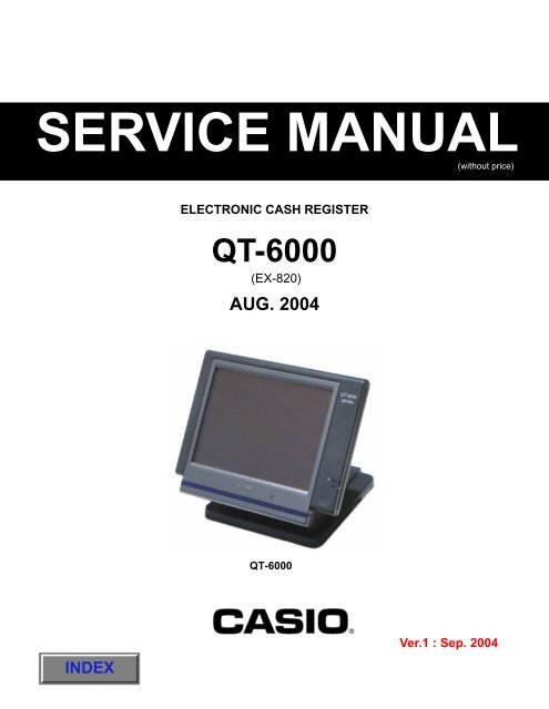
SERVICE MANUAL<br />
(without price)<br />
ELECTRONIC CASH REGISTER<br />
<strong>QT</strong>-<strong>6000</strong><br />
(EX-820)<br />
AUG. 2004<br />
<strong>QT</strong>-<strong>6000</strong><br />
Ver.1 : Sep. 2004
CONTENTS<br />
<strong>QT</strong>-<strong>6000</strong><br />
PAGE<br />
1. SPECIFICATIONS........................................................................................ 1<br />
2. INITIALIZATION ........................................................................................... 5<br />
3. DISASSEMBLY ............................................................................................ 9<br />
4. ASSEMBLY ................................................................................................ 15<br />
5. OPTION INSTALLATION........................................................................... 21<br />
6. IN LINE / ON LINE ..................................................................................... 27<br />
7. DIAGNOSTIC OPERATION ....................................................................... 29<br />
8. CIRCUIT EXPLANATIONS ........................................................................ 51<br />
9. ERROR CODE LIST................................................................................... 79<br />
10. IC DATA ..................................................................................................... 91<br />
11. PCB LAYOUT .......................................................................................... 103<br />
12. CIRCUIT DIAGRAMS............................................................................... 106<br />
13. PARTS LIST ............................................................................................. 125<br />
To prevent malfunctions caused by the weak batteries, charge the memory<br />
protection batteries for over 12-hours before installation or after a long-time<br />
vacation (over 30 days).<br />
• Before installation, initialize the terminal and leave it turn on over 12-hours.<br />
• After a long-time vacation, initialize the terminal and restore the program data if<br />
the terminal is in malfunction, and leave it turn on over 12-hours.<br />
• Over 48-hours charging makes the batteries fully charged.
1. SPECIFICATIONS<br />
1-1. Electrical Specifications<br />
120V 220V 230V 240V<br />
• Power consumption<br />
<br />
In operation 1.1A 1.1A 1.1A 1.1A<br />
Display off 0.25A 0.15A 0.14A 0.13A<br />
<br />
In operation 0.9A 0.9A 0.9A 0.9A<br />
Display off 0.5A 0.5A 0.5A 0.5A<br />
• Memory protection Back-up battery NiMH (nickel-metal-hydride)<br />
HHR-21HL3G1B (USA only)<br />
HHR-21HL3G1C (Except USA)<br />
Back-up period 30 days (25 °C)<br />
Battery life<br />
Replace the battery every 5 years.<br />
Recharge time 24 hours (full charge)<br />
• Clock & Calendar Accuracy Within ± 40 sec. Per month (25 °C)<br />
Auto calendar Effective until 2099 A.D.<br />
1-2. Environmental specifications<br />
• Operating temperature 0 °C ~ 40 °C<br />
• Operating humidity 20 % ~ 85 %<br />
• Storage temperature -20 °C ~ 65 °C<br />
• Storage humidity 10 % ~ 85 %<br />
1-3. Main LSI specifications<br />
• CPU Name HD6417751RF240 (SH-4)<br />
Number of control bit 32 bits<br />
• I/O controller Name UPD78F4216AGC8EUDA01<br />
Number of control bit 16 bits<br />
• Gate array Name UPD65945GJ-P16-JEU<br />
• SDRAM Name EDS2532AABH-75L<br />
Capacity<br />
256 Mbits<br />
• Flash ROM Name MBM29QM12DH<br />
Capacity<br />
128 Mbits<br />
• Display controller Name SM712GX020000-AA<br />
• ADPCM speech LSI Name MSM9841GS-2K<br />
• Ethernet controller Name LAN91C113-NE (10/100BASE TX)<br />
• PCMCIA controller Name R5C485-LQFP144<br />
— 1 —
1-4. Devices specifications<br />
• LCD Display Name NL8060BC31-27<br />
Size 12.1 inch SVGA TFT panel<br />
Resolution 800 x 600<br />
Interface CMOS 6 bits<br />
Colors 262,144 colors<br />
• Touch Panel Name N010-0550-T711<br />
Size 12.1 inch<br />
• Panel brightness control<br />
1 x VR controller<br />
• Speaker 0.5 watt x 1<br />
• Microphone<br />
• Power supply<br />
• Cleck key<br />
Mini electret condenser microphone "EM100TW-ER"<br />
External adaptor "ADP820AA"<br />
Magnetic ibutton prove "94-J-04"<br />
1-5. I/O Ports<br />
COM port (D sub 9pin) x 6<br />
LAN port (Ethernet 10BASE-T/100BASE-TX) x 1<br />
PC CARD slot x 1<br />
CF CARD slot x 1<br />
Drawer port x 2<br />
External speaker jack x 1 (ø3.5 mono)<br />
External microphone jack x 1 (ø3.5 mono)<br />
Card slot cover<br />
PC CARD slot, CF CARD slot<br />
Inline (10/100Base-T)<br />
From the AC adaptor<br />
LAN1<br />
VOL<br />
DC IN PC/MODEM SCANNER DISPLAY DRW1 DRW2<br />
COM1<br />
COM4<br />
COM2<br />
COM5<br />
COM3<br />
COM6<br />
SPK<br />
MIC<br />
Drawer 2<br />
Drawer 1<br />
Ext. microphone<br />
Ext. speaker<br />
COM1 COM4 COM2 COM5 COM3 COM6<br />
— 2 —
1-6. Option List<br />
<strong>CASIO</strong> sales options<br />
DEVICE NAME MODEL NOTE<br />
• Magnet i-Button<br />
<strong>QT</strong>-6011DLS<br />
• Display set for customer <strong>QT</strong>-6060D Connect to Com 3<br />
• Display cable for customer <strong>QT</strong>-6061CB<br />
(for mounting to the base)<br />
• Display 5-meter cable for customer <strong>QT</strong>-6062CB<br />
• Slip printer SP-1300 Connect to Com 2, 3 or 4<br />
• Slip printer cable PRT-CB-8C Length 1.5m<br />
• Remote printer UP-250 Connect to Com 2, 3, 4, 5 or 6<br />
• Remote printer UP-350 Connect to Com 2, 3, 4, 5 or 6<br />
• Remote printer SA-3015 Connect to Com 2, 3, 4, 5 or 6<br />
• Remote printer UP-360 Connect to Com 2, 3, 4, 5 or 6<br />
• Printer cable PRT-CB-8A Length 3m<br />
• Printer cable PRT-CB-8B Length 5m<br />
• Power unit for External Printer PS-180 EPSON MODEL<br />
• Handy scnner HHS-15 Com2 port only<br />
• MCR<br />
<strong>QT</strong>-6046MCR<br />
• Drawer cable <strong>QT</strong>-6031CB Length 3m<br />
• PC cable PRL-CB-2 Com1 port only<br />
Local purchase options<br />
DEVICE NAME MAKER MODEL NOTE<br />
• Slip printer/ AC adaptor AD31-U or E U: 100V / E: 200V<br />
• Remote printer EPSON TM-T88 lll Connect to Com 2, 3, 4, 5 or 6<br />
• Remote printer EPSON TM-U220 Connect to Com 2, 3, 4, 5 or 6<br />
• Power cord for power unit EPSON AC-170<br />
• Laser scanner PSC QuickScan<strong>6000</strong> Com2 port only<br />
• Handy scnner PSC HS1250 Com2 port only<br />
• CF Memory card Sandisk SDCFB-xx-505<br />
• Modem U.S.Robotics 56k FAX<br />
• ISDN TA DEVOLO MICROLINK ISDN<br />
• HUB NETGEAR DS104, DS108<br />
• Wireless LAN card NETGEAR WG551<br />
• Access Point NETGEAR WG602<br />
• External speaker ELECOM MS-76CH<br />
• External microphone ELECOM MS-STM55<br />
• For external speaker / microphone Ohm Electric AP-2633<br />
Stereo-monaural conversion plug<br />
1-7. Drawer<br />
Type Drawer Name Specification USA<br />
Other<br />
Countries<br />
M DL-2785 D-20BC-B84M-15* X<br />
M DL-2786 D-20BC-B84SM-15* X<br />
M DL-2920 D-20BC-B87M-15* X<br />
M DL-2921 D-20BC-B87SM-15* X<br />
M DL-2425 D-20BC-B55SM-15* X<br />
M DL-2525 D-20BC-B64SM-15* X<br />
L DL-3616 D-11BH-B65SS-9* X X<br />
L DL-3617 D-11BH-B65S-9* X<br />
— 3 —
1-8. Duration of Life<br />
Panel of TFT LCD<br />
Back Light of TFT LCD<br />
Touch Panel (number of touch times)<br />
LCD of customer display (option)<br />
Back light of customer display (option)<br />
Head of MCR<br />
50,000 hours<br />
43,000 hours<br />
10 million times<br />
20,000 hours<br />
20,000 hours<br />
300,000 times (in a clean office room)<br />
■ Installing Precautions<br />
When installing <strong>QT</strong>-<strong>6000</strong>, attach the ferrite core to the <strong>QT</strong>-<strong>6000</strong> side. Wind the AC<br />
adaptor cable around the ferrite core two times.<br />
The ferrite core is packed with <strong>QT</strong>-<strong>6000</strong>.<br />
CAUTION<br />
Danger of explosion if battery is incorrectly replaced.<br />
Replace only with the same or equivalent type<br />
recommended by the manufacturer.<br />
Dispose of used batteries according<br />
to the manufacture’s instructions.<br />
VORSICHT !<br />
Explosionsgefahr bei unsachgemäßem Austausch der<br />
Batterie.<br />
Ersatz nur durch denselben oder einen vom<br />
Hersteller empfohlenen gleichwertigen Typ.<br />
Entsorgung gebrauchter Batterien nach<br />
Angaben des Herstellers.<br />
ADVARSEL !<br />
Lithiumbatteri - Eksplosionsfare ved fejlagtig hándtering.<br />
Udskiftning má kun ske med batteri<br />
af samme fabrikat og type.<br />
Levér det brugte batteri tilbage til leverandØren.<br />
— 4 —
2. INITIALIZATION<br />
2-1. MACHINE INITIALIZATION<br />
2-1-1. How to initialize the terminal<br />
Preparation:<br />
1. All peripheral devices and terminals of this cluster should be turned off.<br />
2. Connect all of the peripheral devices (such as printer, display etc.) to terminal.<br />
• In case of wire inline:<br />
3. Connect all terminals by inline.<br />
• In case of wireless inline:<br />
4. Connect Wireless LAN card.<br />
Operation:<br />
5. Turn on all peripheral devices of a terminal.<br />
6. Turn on this terminal with pressing the initialize switch and<br />
release.<br />
Init Sw<br />
INIT<br />
Copyright(C) 2004<br />
<strong>CASIO</strong> COMPUTER CO.,LTD.<br />
All rights reserved.<br />
ROM VER. xxxxxx xxxx<br />
C<br />
7 8 9<br />
CREATE xxxx-xx-xx xx:xx<br />
<strong>QT</strong>-<strong>6000</strong> Version x.xx 4 5 6<br />
APL VER. xxxxxx xxxx<br />
1 2 3<br />
0<br />
OK<br />
7. After releasing the key, enter “20000” (U.S.), “10000” (other area: English), “40000” (other area:<br />
German), “50000” (other area: French), “<strong>6000</strong>0” (other area: Spanish) and press the key.<br />
Enter terminal ID and IP address<br />
ID & IP ADDRESS<br />
Terminal ID<br />
IP ADDRESS<br />
OK?<br />
ENTER ID<br />
AUTO<br />
Yes<br />
——— Terminal ID: 1 ~ 32<br />
——— Press to continue.<br />
• Case 1: Terminal ID = “1”<br />
IP ADDRESS<br />
DHCP<br />
OK?<br />
MANUAL<br />
192.168. 0. 1<br />
SERVER<br />
Yes<br />
——— Enter IP address if you want to change.<br />
——— Select “CLIENT”, if you want to use this terminal as a<br />
DHCP client.<br />
——— Press to continue.<br />
— 5 —
• Case 2: Terminal ID = “2” ~ “32”<br />
IP ADDRESS<br />
OK?<br />
AUTO<br />
Yes<br />
——— Select “MAUAL”, if you want to enter IP address manually.<br />
(IP address setting line will appear on the screen.)<br />
——— Press to continue.<br />
* The IP address of each terminal should be the unique number from 192.168. 0. 1 to 192.168.255.255.<br />
Declare terminal configuration<br />
Date 01-10-10<br />
Time 12:34 00<br />
ID Character MC #01<br />
Check System Master<br />
Check Cluster ID 0<br />
R/J/Order Printer1 No<br />
R/J/Order Printer2 No<br />
R/J/Order Printer3 No<br />
Slip Printer No<br />
——— Enter date if it is wrong.<br />
——— Enter time if it is wrong.<br />
——— Within 12 characters<br />
——— Master / Backup master / Satellite / Self master<br />
——— Enter cluster No. “1” ~ “9”, if using check cluster system.<br />
——— No printer / UP-350 / UP-360 / SA-3015 / UP-250 for<br />
R/J or Order printer.<br />
——— No printer / SA-3015 / SP-1300<br />
OK?<br />
YES<br />
Program restoration<br />
——— Press to continue.<br />
INIT 10-10-01 12:34 000001<br />
AUTO PGM<br />
1.No Restore / Receive<br />
2.PGM Restore (CF Card)<br />
3.PGM Receive (Inline)<br />
——— Select, if no need to download any data.<br />
——— Select to download a program data from CF card.<br />
——— Select to download a program data from other terminal.<br />
• Restore from CF card.<br />
Insert the CF card into the slot and select the appropriate file and press the key.<br />
• Program receive from other terminal.<br />
INIT 10-10-01 12:34 000001<br />
Receive Data<br />
All PGM<br />
——— All Data (including totalizer) / All PGM (program only)<br />
PGM Receive from MC #05<br />
——— Select the machine to send the data.<br />
OK?<br />
YES<br />
Note:<br />
In case of using wireless inline, we recommend that you should change the ESS ID / WEP KEY<br />
character for your security.<br />
2-1-2. How to initialize the terminal (add / replace one terminal)<br />
Preparation:<br />
1. All peripheral devices and terminals of this cluster should be turned off.<br />
2. Connect all of the peripheral devices (such as printer, display etc.) to this terminal.<br />
3. Connect the added / replaced terminal to inline.<br />
Operation:<br />
Follow the steps shown on the page 5 to 6.<br />
— 6 —
2-1-3. How to flag clear the terminal (or INIT2)<br />
Preparation:<br />
1. All peripheral devices and this terminal should be turned off.<br />
2. Check the connection of all peripheral devices (such as printer, display etc.) of this terminal.<br />
3. Check the connection of this terminal to inline.<br />
Operation:<br />
4. Turn on all peripheral devices of this terminal.<br />
5. Turn on this terminal with pressing the key.<br />
6. Press key.<br />
Copyright(C)2004<br />
<strong>CASIO</strong> COMPUTER CO.,LTD.<br />
All rights reserved.<br />
ROM VER xxxxxx xxxx<br />
FC<br />
CREATE xxxx-xx-xx xx:xx<br />
<strong>QT</strong>-<strong>6000</strong> Version x.xx<br />
APL VER. xxxxxx xxxx<br />
OK<br />
7. Select “1. Flag Clear” and press key to flag clear.<br />
or select “2.Init2” and press key and enter “8888888888” and key to Init 2.<br />
2-2. SYSTEM INITIALIZATION<br />
In this chapter shows how to install <strong>QT</strong>-<strong>6000</strong> systems and peripherals.<br />
2-2-1. How to load IPL (Initial Program Loading)<br />
Normally, IPL is not necessary since the terminal has efficient programmable options to<br />
meet your circumstances.<br />
In some cases, you need to change the application program to meet your requirements, the<br />
IPL is necessary to download the application program to the terminal.<br />
To load IPL, there are two methods:<br />
1) From PC to a terminal via RS-232C<br />
2) From CF card to a terminal<br />
— 7 —
2-2-2. IPL Operation<br />
If you select “CF card”, insert the CF card into the slot before this step.<br />
1. Select the appropriate method to loading IPL data.<br />
xxxxxxx<br />
xxxxxxx<br />
xxxxxxx<br />
xxxxxxx<br />
xxxxxxx<br />
xxxxxxx<br />
xxxxxxx<br />
xxxxxxx<br />
IPL :CF CARD<br />
IPL :COM1 PORT<br />
2. If you choose COM port or IN LINE port, select baud rate of the<br />
IPL source device.<br />
xxxxxxx<br />
xxxxxxx<br />
xxxxxxx<br />
IPL :COM1 PORT<br />
115200 bps<br />
57600 bps<br />
5<strong>6000</strong> bps<br />
34800 bps<br />
19200 bps<br />
9600 bps<br />
CANCEL<br />
(using COM PORT)<br />
3. Press the key to proceed, in case of downloading<br />
via inline, automatic ID definition is made by this timing. So<br />
press the key terminal by terminal.<br />
xxxxxxx<br />
xxxxxxx<br />
xxxxxxx<br />
xxxxxxx<br />
xxxxxxx<br />
START<br />
CANCEL<br />
4. After finishing IPL, machine initialization is necessary.<br />
— 8 —
3. DISASSEMBLY<br />
■ <strong>QT</strong>-<strong>6000</strong><br />
1. Separate the main unit and the stand.<br />
2. Remove one screw and the cover.<br />
3. Remove two screws and the cover.<br />
Screws<br />
4. Remove ten screws.<br />
Screw × 10<br />
5. Remove one screw and the lid of the software key.<br />
6. Remove the wiring for the DRAWER (a cable and an earth).<br />
— 9 —
7. Open the CARD SLOT COVER.<br />
8. Remove each screw, and then the PC CARD and the COVER for the CF CARD.<br />
CARD SLOT COVER<br />
Screws<br />
9. Release the hook and remove the REAR CASE.<br />
Be careful with the REAR CASE when removing it since there is a wiring which connects to the speaker.<br />
10. Remove the connector for the speaker.<br />
11. Remove four screws and the iron plate.<br />
12. Remove three screws.<br />
Screw × 4 Screw × 3<br />
13. Remove four connectors, one FPC and the IO unit.<br />
FPC<br />
Connectors<br />
— 10 —
14. Remove the connector for the battery and the battery. 15. Remove four connectors.<br />
Connectors × 4<br />
15. Remove twelve screws and the metal bracket.<br />
Screw × 3 Screw × 3 Screw × 3<br />
Screw × 3<br />
16. Remove three connectors and one FPC.<br />
FPC<br />
Connectors × 3<br />
— 11 —
17. Remove six screws, one connector, one FPC, three bosses, and then remove the main PCB.<br />
Screw × 6<br />
FPC<br />
boss<br />
Connectors<br />
18. Remove 14 screws and then the LCD unit.<br />
Screw × 14<br />
19. Remove two screws, one connector and the inverter PCB.<br />
Screw × 2<br />
Connectors<br />
20. Remove four screws and the LCD.<br />
Screw × 4<br />
The touch panel is fixed by double-sided tape.<br />
— 12 —
■ <strong>QT</strong>-6060D<br />
1. Remove four screws.<br />
2. Release the connector and remove the IO PCB.<br />
Screw × 4<br />
Connector<br />
3. Remove four screws and separate the unit as shown below.<br />
Screw × 4<br />
4. Remove the cap.<br />
5. Remove four screws under both packing.<br />
Screw × 2 Screw × 2<br />
— 13 —
6. Release the hook and remove the REAR CASE.<br />
7. Remove five screws, connector and the HINGE.<br />
Screw × 5<br />
8. Remove seven screws and separate the LCD Unit.<br />
Screw × 7<br />
— 14 —
4. ASSEMBLY<br />
■ <strong>QT</strong>-<strong>6000</strong><br />
1. Place the LCD UNIT in the frame and fix it with four screws.<br />
2. Connect the connector and fix the inverter PCB with two screws.<br />
Screw × 2<br />
3. Fix the LCD UNIT to the FRONT CASE with 14 screws.<br />
Fix the screws from above the earth plate.<br />
Bind the wirings for the inverter.<br />
4. Fix the main PCB with six screws and three bosses.<br />
Screw × 6<br />
FPC<br />
Boss × 3<br />
Connector<br />
— 15 —
5. Connect one PFC and three connector.<br />
Terminal side<br />
Connectors × 3<br />
6. Fix the iron plate with twelve screws.<br />
Screw × 3 Screw × 3 Screw × 3<br />
Screw × 3<br />
7. Connect four connectors.<br />
15. Remove four connectors.<br />
Connectors × 4<br />
— 16 —
8. Connect the connector for the battery and assemble the battery.<br />
9. Assemble the IO Unit and fix it with three screws.<br />
Connect four connectors and one FPC.<br />
Screw × 3<br />
Connectors<br />
FPC<br />
10. Fix the iron plate with four screws.<br />
Screw × 4<br />
— 17 —
11. Connect the connector for the speaker and assemble the REAR CASE.<br />
Hook the REAR CASE and fix it with ten screws.<br />
Screw × 10<br />
12. Fix the PC CARD and the CF CARD COVER.<br />
Fix the backup battery cover with one screw.<br />
Connect the DRAWER wiring (a cable and an earth).<br />
CARD SLOT COVER<br />
Screws<br />
13. Fix the case with two screws.<br />
14. Fix the IP PORT COVER and the stand.<br />
— 18 —
■ <strong>QT</strong>-6060D<br />
1. Assemble the LCD Unit in the FRONT CASE with seven screws.<br />
Screw × 7<br />
2. Connect the connector and fix the HINGE with five screws.<br />
Screw × 5<br />
3. After fixing the packing to the REAR CASE, assemble the REAR CASE and the FRONT CASE.<br />
Hooks<br />
4. Remove the LCD unit with four screws.<br />
Position: under both packing<br />
Screw × 2 Screw × 2<br />
— 19 —
5. Fix the cap to the LCD Unit.<br />
Be careful with the position of the screw holes.<br />
6. Fix the cap to the stand.<br />
Be careful with the direction of the cap. The height of the screw hole on the front side should be lower.<br />
7. Let the connector through the cap and fix the LCD unit with four screws.<br />
Screw × 4<br />
8. Connect the connector and fix the IO Unit with four screws.<br />
Connector<br />
Screw × 4<br />
— 20 —
5. OPTION INSTALLATION<br />
5-1. Installing the display set for customer (EX-DP-UNIT-16)<br />
Metal bracket for type A<br />
Metal bracket for type B<br />
■ There are two types for the display set for customer (EX-DP-UNIT-16).<br />
Type A<br />
Type B<br />
■ To install Type A<br />
1. Remove two screws at the bottom and then the cover.<br />
2. Remove five screws at the bottom and then the metal<br />
bracket.<br />
3. Connect the cable to EX-DP-UNIT-16.<br />
4. Fix the metal bracket for type A with screws.<br />
— 21 —
5. Fix EX-DP-UNIT-16 to the main unit with four screws.<br />
6. Connect the cable to the main unit (COM1).<br />
7. Fix the metal bracket which was removed in the above step 2.<br />
■ To install Type B<br />
1. Remove five screws at the bottom and then the metal<br />
bracket.<br />
2. Fix the metal bracket for type B to the main unit with doublesided<br />
tape.<br />
Position to be fixed: Align the metal bracket in the center of<br />
the main unit and fix it where it is 1.0cm from the edge.<br />
3. Connect the cable to EX-DP-UNIT-16.<br />
4. Fix the main unit to the metal bracket for type B.<br />
5. Connect the cable to the main unit (COM1).<br />
6. Fix the metal bracket which was removed in the above step 1.<br />
— 22 —
■ LONG POLE<br />
It is possible to attach the long pole in <strong>QT</strong>-6060D.<br />
Please arrange the following parts at your side when you need them.<br />
Status in 4<br />
Attachment parts (arranged by dealers)<br />
LONG-POLE (arranged by dealers)<br />
1 Turn the DP-UNIT-16 over.<br />
2 Remove four pan-head screws which are fixed in<br />
STD-POLE.<br />
(This separates DP/STAND ASSY.)<br />
3 Remove four tapping screws to remove the chassis<br />
from the STAND ASSY.<br />
4 Fix STD-POLE and ROTARY-SHAFT to DP-ASSY<br />
with four pan-head screws.<br />
5 Fix the part arranged by dealers.<br />
Reference Drawing<br />
— 23 —
5-2. To install the I-Button<br />
1. Remove the REAR COVER for <strong>QT</strong>-<strong>6000</strong> (No.1 to No.10 in the disassembly procedure).<br />
2. Remove one screw and then the I-Button cover.<br />
3. Insert the I-Button. Fix it with a nut. Insert the earth plate. Fix it with a nut.<br />
4. Assemble the lead wire (earth) into the connector.<br />
5. Wind the lead wire around the core twice, and then connect the core to the connector of the main unit.<br />
— 24 —
6. Store the core in the main unit, and then fix it with fabric tape.<br />
5-3. To install the MCR<br />
1. Remove the REAR COVER for <strong>QT</strong>-<strong>6000</strong> (No.1 to No.10 in the disassembly procedure).<br />
2. Remove the packing from the main unit.<br />
3. Insert the MCR into the special metal bracket.<br />
NOTE: Be careful not to damage the FPC.<br />
4. Connect the connector and fix the metal bracket with two screws.<br />
NOTE: The lead wires should be stored neatly in a line.<br />
— 25 —
5. Fix the metal bracket to <strong>QT</strong>-<strong>6000</strong> with two screws.<br />
6. Connect the connector to <strong>QT</strong>-<strong>6000</strong>.<br />
NOTE: Arrange the cables so that they do not tangle with each other.<br />
5-4. REMOTE PRINTER / SLIP PRINTERSCANNER<br />
5-5. HANDY SCANNER<br />
Card slot cover<br />
PC CARD slot, CF CARD slot<br />
Connect the following peripherals<br />
to the COM ports respectively.<br />
REMOTE PRINTER: COM2, 3,<br />
4, 5 or 6 / SLIP PRINTER: COM2,<br />
3 or 4<br />
HANDY SCANNER: COM2<br />
From the AC adaptor<br />
LAN1<br />
DC IN PC/MODEM SCANNER DISPLAY DRW1 DRW2<br />
COM1<br />
COM2<br />
COM3<br />
Inline (10/100Base-T)<br />
VOL<br />
MIC<br />
Drawer 2<br />
Drawer 1<br />
COM4<br />
COM5<br />
COM6<br />
SPK<br />
Ext. microphone<br />
Ext. speaker<br />
COM1 COM4 COM2 COM5 COM3 COM6<br />
5-6. To install the DRAWER<br />
In case of connecting drawer, follow the procedure below.<br />
1. Connect drawer connector (three color lead on drawer) to the terminal.<br />
2. Connect frame drawer connector (green lead on drawer) to the terminal.<br />
Mount the cash register.<br />
1. Screw in 2 fixing screws bottom side of the terminal.<br />
2. Mount the terminal on the top of the drawer, ensuring that the feet on the<br />
bottom of the terminal go into the holes on the drawer.<br />
— 26 —
6. IN LINE / ON LINE<br />
With the <strong>QT</strong>-<strong>6000</strong>, there are the following inline / online connectors in the rear side of the body.<br />
6-1. Inline interface<br />
The maximum inline cable length and the maximum connection unit will be varied by the inline communication<br />
speed as shown below figure.<br />
• Using 10BASE-T<br />
Cable length: 100m (terminal to terminal, hub to terminal, hub to hub)<br />
Maximum 4 hubs in one cluster.<br />
Maximum cable length between terminal and terminal via hubs is 500m.<br />
• Using 100Base-TX<br />
Cable length: 100m (terminal to terminal, hub to terminal, hub to hub)<br />
Maximum 2 hubs in one cluster.<br />
Maximum cable length between terminal and terminal via hubs is 300m.<br />
Terminal to terminal<br />
• 10BASE-T<br />
• 100BASE-TX<br />
Max.100m<br />
CAT5 cable specifications<br />
CAT5 UTP Cable (Straight)<br />
0.5mm x 4P Not shielded wire Twist pair cable<br />
Configuration with Hub<br />
• 10BASE-T<br />
• 100BASE-TX<br />
Max.100m Max.100m Max.100m Max.100m Max.100m<br />
Max.100m<br />
Max.100m<br />
Max.100m<br />
Maximum 32 terminals Max.500m<br />
Maximum 32 terminals Max.300m<br />
6-2. Wireless LAN<br />
There is a PC CARD SLOT in <strong>QT</strong>-<strong>6000</strong> and a wireless LAN CARD can be installed to the PC CARD SLOT.<br />
The specifications are as shown below figure.<br />
The maximum communication distance is 20m.<br />
The maximum number of terminals which can be accessed to one wireless access point is eight.<br />
The effective distance between the wireless access point and the terminal is 20 meters where there is no major<br />
obstacle.<br />
(Precautions regarding the installation of the wireless access point)<br />
Install the terminal away from the following which may cause interference; PC, large metal, microwave, cordless<br />
telephone at 2.4GHz, etc.<br />
Install the terminal in the center of the area where you want to connect to the terminal wirelessly, as well as<br />
install it on a high place such as on a rack.<br />
HUB (Option)<br />
Wireless Access Point (Otion)<br />
Max. 20m<br />
Maximum 8 terminals in Wireless Access Point<br />
— 27 —
6-3. Online interface<br />
Only the RS-232C Com1 port can be connected with a modem or perssonal computer.<br />
Direct connection to PC<br />
1 Connection layout<br />
Note: Maximum 3 remote printers in the 1<br />
terminal system, 6 remote printers / 2<br />
terminal system, 8 remote printers in<br />
PC<br />
the 3 ~ 32 terminal can be defined.<br />
Via COM 1 port of the master terminal<br />
or Inline (Ethernet)<br />
Maximum 32 terminals<br />
2 PC Cable wiring<br />
<strong>QT</strong>-<strong>6000</strong> (Com1)<br />
Pin No. Signal name<br />
3 SD/TXD<br />
2 RD/RXD<br />
7 RS/RTS<br />
8 CS/CTS<br />
1 CD/DCD<br />
4 ER/DTR<br />
6 DR/DSR<br />
9 CI/RI<br />
5 GND<br />
PC<br />
Pin No. Pin No. Signal name<br />
(DSUB9) (DSUB25)<br />
3 2 SD<br />
2 3 RD<br />
7 4 RS<br />
8 5 CS<br />
1 8 CD<br />
4 20 ER<br />
6 6 DR<br />
- 22 C<br />
5 7 GND<br />
MODEM system<br />
1 Connection layout<br />
Note: Maximum 3 remote printers in<br />
the 1 terminal system, 6 remote<br />
printers / 2 terminal system, 8 remote<br />
printers in the 3 ~ 32 terminal<br />
can be defined.<br />
PC<br />
on-line<br />
Maximum 32 terminals<br />
2 PC Cable wiring<br />
<strong>QT</strong>-<strong>6000</strong> (Com1)<br />
Pin No. Signal name<br />
3 SD/TXD<br />
2 RD/RXD<br />
7 RS/RTS<br />
8 CS/CTS<br />
1 CD/DCD<br />
4 ER/DTR<br />
6 DR/DSR<br />
9 CI/RI<br />
5 GND<br />
MODEM (DSUB25)<br />
Pin No. Signal name<br />
2 SD<br />
3 RD<br />
4 RS<br />
5 CS<br />
8 CD<br />
20 ER<br />
6 DR<br />
22 CI<br />
7 GND<br />
— 28 —
7. DIAGNOSTIC OPERATION<br />
7-1. To start the diagnostic program<br />
(1) Turn the power off.<br />
(2) Turn the power on while pressing the INIT switch.<br />
Init Sw<br />
(3) Release the switch when the display shown below appears.<br />
* Operation is not guaranteed if the switch is released before the display appears.<br />
INIT<br />
Copyright(C)2004<br />
<strong>CASIO</strong> COMPUTER CO.,LTD.<br />
All rights reserved.<br />
ROM VER xxxxxx xxxx<br />
C<br />
7 8 9<br />
CREATE xxxx-xx-xx xx:xx<br />
<strong>QT</strong>-<strong>6000</strong> Version x.xx 4 5 6<br />
APL VER. xxxxxx xxxx<br />
1 2 3<br />
0<br />
OK<br />
(4) Enter 99990000 and then [OK].<br />
(5) LCD calibration test starts automatically.<br />
Refer to "[ 12 ] LCD calibration test" for the operation details.<br />
7-2. Notes for the DIAG<br />
• Make sure the printer used to print out test results is set to a baud rate of 9600 bps and is connected<br />
to COM4.<br />
• Perform testing by connecting HHS-15 to COM2.<br />
• Always make sure to connect REMOTE DISP to COM3.<br />
• When desiring to conduct a test for an unlimited number of times, enter a value other than 0 in<br />
accordance with the explanation for each test. Tests are performed for an unlimited number of times<br />
when a value of 1 through 9 is entered for the commend used to specify the number of times testing<br />
is performed in the operating procedure on each page. However, this function allows a test to only<br />
be performed once or for an unlimited number times.<br />
[Procedure and Display for Operator-Evaluated Tests]<br />
• In operator-evaluated tests, the results for that test are determined according to the OK and NG keys<br />
after the following display appears.<br />
[OK] key: Register 1 [NG] key: Register 9<br />
• A display that excludes the following display is shown for the LCD display of each test.<br />
| Please Hit Key OK-> 1 NG-> 9 |<br />
[Other]<br />
* ESC printout and display contents for forced termination of a test by ESC are as shown below. This<br />
display and printout are omitted in each test.<br />
| ESC |<br />
* That following printing of test results is omitted.<br />
— 29 —
7-3. DIAG command input system<br />
Input a command according to the following code.<br />
X X X X X X n a g d<br />
XXXXXX : additional action<br />
n : number of times<br />
a : action<br />
g : group<br />
d : device number<br />
7-4. Status Display<br />
With the EX820, the following display is displayed on<br />
the LCD (SVGA). (In this DIAG, the display area is<br />
divided into a display for register entry and a display<br />
of DIAG results and so forth.<br />
DALLAS<br />
DRW1 CLOSE<br />
0000<br />
MENU SHEET 1<br />
DRW2 CLOSE<br />
CLR<br />
ESC<br />
7 8 9<br />
4 5 6<br />
1 2 3<br />
0 ST<br />
[Functions]<br />
Status is displayed for those devices having status information. The devices and status displayed<br />
are as shown below.<br />
Device<br />
Status Information (Displayed Information)<br />
Dallas key<br />
Dallas key no.<br />
Dallas key 2<br />
Dallas key no.<br />
Drawer<br />
Open/close status<br />
MAC address<br />
MAC address<br />
CF<br />
Insertion status<br />
DISP ON/OFF switch Switch status<br />
TEMP<br />
Poxwer supply A/D conversion value<br />
* Display only updated when DISP ON/OFF switch is ON<br />
[LCD Display]<br />
MAC ADRS XX-XX-XX-XX-XX-XX<br />
CF INSERT<br />
DISP ON/OFF ON TEMP 20<br />
Status information is displayed continuously (in ordinary characters).<br />
However, when performing a test, the status at completion of a test is<br />
displayed following completion of that test.<br />
Diag Ver : XXXXXX XXXX<br />
DALLAS<br />
DRW1 CLOSE<br />
DRW2 CLOSE<br />
0000 1234<br />
Register: Characters enlarged 1.5 times (max. 10 digits)<br />
Counter display<br />
* Addition of TEMP information and DISP ON/OFF status<br />
The TEMP status is acquired preferentially when the DISP ON/OFF switch is ON. When measuring<br />
other status information or when starting each test mode, always make sure to begin after switching<br />
off the DISP ON/OFF switch.<br />
— 30 —
7-5. Check item<br />
The following test can be checked in the diagnostic test.<br />
No Device to be checked Operation Note Page<br />
1 Batch test 1 2 Test Device : RAM, FLASH, Display, 32<br />
Print, Time, Drawer<br />
2 Batch test 2 3 Test Device : Display, Back light 32<br />
3 RAM WRITE/READ test n011 33<br />
4 RAM READ only test n111 33<br />
5 FLASH Check SUM test n512 34<br />
6 FLASH CLEAR/WRITE/READ test n612 34<br />
7 CF-CARD WRITE/READ test pn013 35<br />
8 CF-CARD READ only test pn113 35<br />
9 CF-CARD CLEAR test pn213 36<br />
10 CF-CARD CLEAR&WRITE/READ test pn313 36<br />
11 LCD test n021 37<br />
12 LCD calibration test 221 38<br />
13 Back light OFF test 121 38<br />
14 Remote Cust DISP test bn023 39<br />
15 External printer print test x1x2x3n03d 40<br />
16 RS232C PORT test xn04d 41<br />
17 RS232C PORT batch test 40 42<br />
18 Ethernet test m0a51 43<br />
19 MAC Address SET x0951 44<br />
20 Wireless LAN test m0a52 45<br />
21 Time setting x1x2x3x4x5x60a70 46<br />
22 Time display 70 46<br />
23 Drawer open test xn091 46<br />
24 Buzzer test n092 47<br />
25 OBR test 95 47<br />
26 MCR test 96 48<br />
27 Sound playback test axn097 49<br />
28 Sound recording test 98 50<br />
29 Charging test 99 50<br />
— 31 —
7-6. Operation of each test<br />
[ 1 ] Batch test 1<br />
[Function]<br />
RAM test, FLASH test, display test, test print, time setting and drawer open test are performed<br />
continuously.<br />
Make sure to connect the printer to COM4.<br />
[Operation]<br />
Refer to the page for the details of the following tests.<br />
Operation : 2 ST<br />
The following tests are performed automatically.<br />
(1) RAM test : WRITE/READ all block test<br />
(2) FLASH : Check SUM test<br />
(3) Test print<br />
(4) Times setting : Set the following data.<br />
Arranged data : 2001 December 31, 23:59’30<br />
(5) Drawer open : Opens all drawer.<br />
Enters the wait mode for the input of [OK] or [NG] by the operator after drawer open.<br />
(6) Receipt issuance<br />
[LCD]<br />
*When normally printed<br />
BATC H 2<br />
RAM WR OK<br />
FLASH CHK SUM OK<br />
DATE 01/12/31<br />
TIME 23:59-30<br />
Please Hit Key OK->1 NG->9<br />
DRW ALL OK<br />
END 2<br />
[Print]<br />
*When normally printed<br />
BATC H 2<br />
RAM WR OK<br />
FLASH CHK SUM OK<br />
BBBBBBBBBBBBBBBBBBBB *8,888,88<br />
DATE 01/12/31<br />
TIME 23:59-30<br />
DRW ALL OK<br />
END 2<br />
Print Test<br />
[ 2 ] Batch test 2<br />
[Function]<br />
LCD display test and backlight test are performed continuously.<br />
[Operation]<br />
Refer to the page for the details of the following tests.<br />
Operation : 3 ST<br />
The following tests are performed automatically.<br />
(1) LCD test :<br />
Enters the wait mode for the input of [OK] or [NG] by the operator after the test.<br />
"OK" = 1, "NG" = 9<br />
(2) Backlight OFF test :<br />
Turns the backlight off.<br />
Enters the wait mode for the input of [OK] or [NG] by the operator after the backlight turns off.<br />
*Since the backlight is turned off, "Please Hit Key…" cannot be seen.<br />
"OK" = 1, "NG" = 9<br />
(3) Receipt issuance<br />
[LCD]<br />
*When normally printed<br />
[Print]<br />
*When normally printed<br />
BATCH 3<br />
Please Hit Key OK->1 NG->9<br />
LCD<br />
OK<br />
Please Hit Key OK->1 NG->9<br />
BACK LIGHT OK<br />
END 3<br />
Waiting for the input of [OK] or<br />
[NG] for the LCD test.<br />
Waiting for the input of [OK] or<br />
[NG] for the backlight.<br />
* When this appears, the backlight<br />
is turned off.<br />
BATC H 3<br />
LCD<br />
OK<br />
BACK LIGHT OK<br />
END 3<br />
— 32 —
[ 3 ] RAM WRITE/READ test<br />
[Function]<br />
WRITE/READ test for RAM is performed.<br />
A counter is displayed for RAM test as follows.<br />
[Operation]<br />
Operation : n 0 1 1 ST<br />
n: 0 = One time check (can be omitted)<br />
not 0 = Continuous check (To stop the test, press "ESC" key)<br />
[LCD]<br />
RAM<br />
n011<br />
NOTE: Prints the address of the error in case the test ended<br />
with an error.<br />
RAM WR<br />
END<br />
OK<br />
n011<br />
[PRINT]<br />
RAM<br />
RAM WR<br />
END<br />
n011<br />
NG<br />
n011<br />
Prints the address of the error in case the test ended with an<br />
error.<br />
[ 4 ] RAM READ ONLY test<br />
[Function]<br />
READ ONLY test for RAM is performed<br />
Note that WRITE test (n011) must be performed right before this test.<br />
[Operation]<br />
Operation : n 1 1 1 ST<br />
n: 0 = One time check (can be omitted)<br />
not 0 = Continuous check (To stop the test, press "ESC" key)<br />
[LCD]<br />
NOTE: Prints the address of the error in case the test ended<br />
RAM<br />
n111<br />
with an error.<br />
RAM RD<br />
END<br />
OK<br />
n111<br />
[PRINT]<br />
RAM<br />
RAM RD<br />
END<br />
n111<br />
OK<br />
n111<br />
Prints the address of the error in case the test ended with an<br />
error.<br />
— 33 —
[ 5 ] FLASH Check SUM test<br />
[Function]<br />
This test will check SUM test for FLASH is performed.<br />
[Operation]<br />
Operation : n 5 1 2 ST<br />
n: 0 = One time check (can be omitted)<br />
not 0 = Continuous check (To stop the test, press "ESC" key)<br />
[LCD]<br />
FLASH 512<br />
FLASH CHK SUM OK<br />
END 512<br />
[PRINT]<br />
FLASH 512<br />
FLASH CHK SUM OK<br />
END 512<br />
[ 6 ] FLASH CLEAR WRITE/READ test<br />
[Function]<br />
The CLEAR & WRITE/READ test for FLASH is performed.<br />
After deleting the memory by CLEAR, WRITE/READ test is performed.<br />
Note: since this test cannot backup the program, you need to perform IPL again after the test.<br />
When the memory in the FLASH memory is cleared (by the CLEAR test), the program is<br />
cleared also.<br />
[Operation]<br />
Operation : n 6 1 2 ST<br />
n: 0 = One time check (can be omitted)<br />
not 0 = Continuous check (To stop the test, press "ESC" key)<br />
[LCD]<br />
NG and the address are displayed if WRITE cannot be done<br />
FLASH 612<br />
normally.<br />
FLASH WR ERASE PGM OK<br />
END 612<br />
[PRINT]<br />
FLASH 612<br />
FLASH WR ERASE PGM OK<br />
END 612<br />
NG and the address are printed if WRITE cannot be done<br />
normally.<br />
— 34 —
[ 7 ] CF-CARD WRITE/READ test<br />
[Function]<br />
This test will check the write/read test (connection test) for CF-CARD.<br />
Perform the CF-CARD clear test, before start of this test.<br />
Note that this test does not ensure the data inside the CF-CARD as well as its performance.<br />
[Operation]<br />
Operation : p n 0 1 3 ST<br />
p : designates PCMCIA SLOT<br />
0 = CF<br />
1 = PCMCIA<br />
n: 0 = One time check (can be omitted)<br />
not 0 = Continuous check (To stop the test, press "ESC" key)<br />
[LCD]<br />
NG and the address are displayed if WRITE cannot be done<br />
CF-CARD pn013<br />
normally.<br />
CF WR<br />
END<br />
OK<br />
pn013<br />
[PRINT]<br />
CF<br />
CF WR<br />
END<br />
pn013<br />
OK<br />
pn013<br />
NG and the address are printed if WRITE cannot be done<br />
normally.<br />
[ 8 ] CF-CARD READ ONLY test<br />
[Function]<br />
This test will check the read only test for CF-CARD.<br />
Perform the CF-CARD write test, before start of this test.<br />
Note that this test does not ensure the data inside the CF-CARD as well as its performance.<br />
[Operation]<br />
Operation : p n 1 1 3 ST<br />
p: designates PCMCIA SLOT<br />
0 = CF<br />
1 = PCMCIA<br />
n: 0 = One time check (can be omitted)<br />
not 0 = Continuous check (To stop the test, press "ESC" key)<br />
[LCD]<br />
NG and the address are displayed if READ cannot be done<br />
CF-CARD pn113<br />
normally.<br />
CF RD<br />
END<br />
OK<br />
pn113<br />
[PRINT]<br />
CF-CARD<br />
CF RD<br />
END<br />
pn113<br />
OK<br />
pn113<br />
NG and the address are printed if WRITE cannot be done<br />
normally.<br />
— 35 —
[ 9 ] CF-CARD CLEAR test<br />
[Function]<br />
This test will check the clear test for CF-CARD.<br />
Note that this test does not ensure the data inside the CF-CARD as well as its performance.<br />
[Operation]<br />
Operation : p n 2 1 3 ST<br />
p: designates PCMCIA SLOT<br />
0 = CF<br />
1 = PCMCIA<br />
n: 0 = One time check (can be omitted)<br />
not 0 = Continuous check (To stop the test, press "ESC" key)<br />
[LCD]<br />
NG and the address are displayed if CLEAR cannot be done<br />
CF-CARD pn213<br />
normally.<br />
CF CLR<br />
END<br />
OK<br />
pn213<br />
[PRINT]<br />
CF-CARD<br />
CF CLR<br />
END<br />
pn213<br />
OK<br />
pn213<br />
NG and the address are printed if WRITE cannot be done<br />
normally.<br />
[ 10 ] CF-CARD CLEAR WRITE/READ test<br />
[Function]<br />
The CLEAR & WRITE/READ test for CF-CARD is performed.<br />
After deleting the memory by CLEAR, WRITE/READ test (connection test) is performed.<br />
Note that this test does not ensure the data inside the CF-CARD as well as its performance.<br />
[Operation]<br />
Operation : p n 3 1 3 ST<br />
p: designates PCMCIA SLOT<br />
0 = CF<br />
1 = PCMCIA<br />
n: 0 = One time check (can be omitted)<br />
not 0 = Continuous check (To stop the test, press "ESC" key)<br />
[LCD]<br />
NG and the address are displayed if WRITE cannot be done<br />
CF-CARD pn313<br />
normally.<br />
CF CLR&WR<br />
END<br />
OK<br />
pn313<br />
[PRINT]<br />
CF-CARD<br />
CF CLR&WR<br />
END<br />
pn313<br />
OK<br />
pn313<br />
NG and the address are printed if WRITE cannot be done<br />
normally.<br />
— 36 —
[ 11 ] LCD test<br />
[Function]<br />
This test will check the LCD display.<br />
In case of one time check only, the test can be ended by the judgment (OK or NG) of the operator.<br />
The display can be switched by the touch of the panel. The display will not change to the next one<br />
unless the panel is touched.<br />
[Operation]<br />
Press [OK] key or [NG] key to end the test when performing one time check.<br />
"OK" = 1, "NG" = 9<br />
Operation : n 0 2 1 ST<br />
n: 0 = One time check (can be omitted)<br />
not 0 = Continuous check (To stop the test, press "ESC" key)<br />
[LCD]<br />
Black<br />
White<br />
Red<br />
Green<br />
Blue<br />
Check (black<br />
and white)<br />
Reverse<br />
check<br />
Touch any place<br />
in the panel.<br />
Touch any place<br />
in the panel.<br />
Touch any place<br />
in the panel.<br />
Touch any place<br />
in the panel.<br />
Touch any place<br />
in the panel.<br />
Touch any place<br />
in the panel.<br />
Shows the following colors and patterns in the display in the order of black, white, red, green, blue,<br />
check and reverse check.<br />
Returns to the normal display after the test, and waits for the input of [OK] or [NG] by the operator<br />
(in case of one time check).<br />
In case of continuous check, the test is ended manually upon the input of [ESC] key.<br />
LCD<br />
LCD<br />
END<br />
n021<br />
OK<br />
n021<br />
[PRINT]<br />
LCD<br />
LCD<br />
END<br />
n021<br />
OK<br />
n021<br />
— 37 —
[ 12 ] LCD calibration test<br />
[Function]<br />
This will test the calibration of the LCD (touch panel).<br />
* Perform the calibration in the diagnostic mode even when the product is in the market. Make sure<br />
to backup the register data when necessary.<br />
[Operation]<br />
A cross appears at the following four coordinates in the panel one by one. When a cross at a certain<br />
coordinate is touched, the next coordinate will show another cross there.<br />
(X,Y) = (100,100), (100,500), (700,100), (700,500)<br />
Operation : 2 2 1 ST<br />
If X4 or Y4 data goes out of the following tolerance, the test will be NG.<br />
Please test again.<br />
X4: 700±12 Y4: 500±12<br />
[LCD]<br />
TOUCH START 221<br />
(X1,Y1) : (XXX,XXX)<br />
(X2,Y2) : (XXX,XXX)<br />
(X3,Y3) : (XXX,XXX)<br />
(X4,Y4) : (XXX,XXX)<br />
END 221<br />
Displays data 1 for calibration<br />
Displays data 2 for calibration<br />
Displays data 3 for calibration<br />
Displays the position of the forth coordinate (performs calibration)<br />
How to skip the calibration test.<br />
(LCD)<br />
Enter the Caribration mode<br />
Push Disp on/off key<br />
Skip the Caribration mode<br />
Touch the panel<br />
To perform the caribration test : Push disp on/off key<br />
To skip the caribration test : Touch the panel<br />
[PRINT]<br />
TOUCH START 221<br />
(X1,Y1) : (XXX,XXX)<br />
(X2,Y2) : (XXX,XXX)<br />
(X3,Y3) : (XXX,XXX)<br />
(X4,Y4) : (XXX,XXX)<br />
END 221<br />
[ 13 ] LCD Backlight OFF test<br />
[Function]<br />
This is a test for the LCD backlight.<br />
The test ends upon judgment of the operator between [OK] and [NG].<br />
[Operation]<br />
Press [OK] key or [NG] key to end the test when performing one time check.<br />
"OK" = 1, "NG" = 9<br />
Operation : 1 2 1 ST<br />
[LCD]<br />
[PRINT]<br />
BACK LIGHT 121<br />
BACK LIGHT OK<br />
END 121<br />
BACK LIGHT 121<br />
BACK LIGHT OK<br />
END 121<br />
— 38 —
[ 14 ] Remote Cust DISP test<br />
[Function]<br />
This test will check whether REMOTE DISP can be displayed.<br />
Make sure to connect REMOTE DISP to COM3.<br />
In case of one time check only, the test can be ended by the judgment (OK or NG) of the operator.<br />
Pastel green (white plus green) appears as the backlight, which turns off upon the end of the test.<br />
* When changing the baud rate, make sure to change the REMOTE DISP setting.<br />
[Operation]<br />
Press [OK] key or [NG] key to end the test when performing one time check.<br />
"OK" = 1, "NG" = 9<br />
Operation : b n 0 2 3 ST<br />
b: Baud rate selection<br />
0 = 19.2 Kbps, 1 = 9600 bps<br />
n: 0 = One time check (can be omitted)<br />
not 0 = Continuous check (To stop the test, press "ESC" key)<br />
When performing continuous check, the same test character data is sent at a certain interval. When<br />
the test is ended manually upon the input of [ESC] key, the display is cleared and the backlight turns<br />
off.<br />
In case of one time check, the display is cleared and the backlight turns off after the judgment ([OK]<br />
or [NG]) of the operator.<br />
[LCD]<br />
REMOTE DISP<br />
REMOTE DISP<br />
END<br />
na23<br />
OK<br />
na23<br />
[REMOTE DISP]<br />
ABCDEFGHIJKLMNOP<br />
QRSTUVWXYZabcdef<br />
0,1,2,3,4,5,6,7,8,9,<br />
[PRINT]<br />
REMOTE DISP<br />
REMOTE DISP<br />
END<br />
na23<br />
OK<br />
na23<br />
— 39 —
[ 15 ] External printer print test<br />
[Function]<br />
This test will check the print test for the RS232C I/F printer.<br />
Connect the printer to the COM which is to be tested.<br />
[Operation]<br />
Operation : x1 x2 x3 n 0 3 d ST<br />
X1:Print test pattern (0 = A pattern, 1 = B pattern)<br />
X2:Port selection (1 = COM1, 2 = COM2, 3 = COM3, 4 = COM4, 5 = COM5, 6 = COM6)<br />
X3:Baud rate selection (1 = 4800 bps, 2 = 9600 bps, 3 = 19.2 kbps)<br />
n: 0 = One time check (can be omitted)<br />
not 0 = Continuous check (To stop the test, press "ESC" key)<br />
d: Printer type selection (1 = RJ, 2 = SLIP)<br />
Note that some printers cannot use certain baud rates. Refer to the list below.<br />
When changing the baud rate, make sure to change the setting for the printer also.<br />
[LCD]<br />
19.2 Kbps 9600 bps 4800 bps<br />
SLIP PRINTER (SP1300) ✕ Ο Ο<br />
RJ PRINTER (UP250/350/360) Ο Ο Ο<br />
PRT<br />
END<br />
xxxn03d<br />
xxxn03d<br />
Error display<br />
When the printer is not connected<br />
NON PRINTER ERR<br />
[PRINT]<br />
Printing pattern is the following 2 types.<br />
The number of lines : 40 lines for RJ and 35 lines for SLIP.<br />
BBBBBBBBBBBBBBBBBBBBBBBBBBBBBBBBB<br />
BBBBBBBBBBBBBBBBBBBBB *8,888,88<br />
A pattern<br />
B pattern<br />
— 40 —
[ 16 ] RS232C PORT test<br />
[Function]<br />
This is the RS232C test.<br />
The loop back test for RS232C port is performed by making the connection shown in the figure.<br />
Refer to [ 17 ] RS232C PORT batch test the figure for RS232C port connection.<br />
[Operation]<br />
Operation : x n 0 4 d ST<br />
x: Baud rate selection<br />
0 = 2400 bps, 1 = 4800 bps, 2 = 9600 bps, 3 = 19.2 kbps, 7 = 115 kbps (COM 1 only)<br />
n: 0 = One time check (can be omitted)<br />
not 0 = Continuous check (To stop the test, press "ESC" key)<br />
d: Port selection<br />
1 = COM1, 2 = COM2, 3 = COM3, 4 = COM4, 5 = COM5, 6 = COM6<br />
[LCD]<br />
COM 41<br />
RTS1=1 CTS1=1 OK<br />
DTR1=1 DSR1=1 OK<br />
DTR1=1 CD1=1 OK<br />
DTR1=1 CI1=1 OK<br />
RTS1=0 CTS1=0 OK<br />
DTR1=0 DSR1=0 OK<br />
DTR1=0 CD1=0 OK<br />
DTR1=0 CI1=0 OK<br />
TxD RxD OK<br />
END 41<br />
Displays only COM1<br />
Displays only COM1<br />
Displays only COM1<br />
Displays only COM1<br />
— 41 —
[ 17 ] RS232C PORT batch test<br />
[Function]<br />
This is the RS232C port batch test.<br />
The loop back test for RS232C port is performed by making the connection shown in the figure.<br />
The loop back test is performed from COM1 to COM 6 by the following setting by one time check.<br />
When performing this test, fix loop back connectors to all COM ports.<br />
[Operation]<br />
Operation : 4 0 ST<br />
Baud rate: COM1: 115 kbps, COM 2 – 6 : 9600 bps<br />
Check time: one time<br />
[LCD]<br />
COM BATCH 40<br />
RTS1=1 CTS1=1 OK<br />
DTR1=1 DSR1=1 OK<br />
DTR1=1 CD1=1 OK<br />
DTR1=1 CI1=1 OK<br />
RTS1=0 CTS1=0 OK<br />
DTR1=0 DSR1=0 OK<br />
DTR1=0 CD1=0 OK<br />
DTR1=0 CI1=0 OK<br />
TxD RxD OK<br />
RTS2=1 CTS2=1 OK<br />
DTR2=1 DSR2=1 OK<br />
DTR2=0 CD2=0 OK<br />
DTR2=0 CI2=0 OK<br />
TxD RxD OK<br />
COM 1 test result<br />
COM 2 test result<br />
•<br />
•<br />
•<br />
END 40<br />
The same display for COM2 appears for COM3 to COM6.<br />
Note that the actual display shows only a part of the results (not the whole as shown in the left).<br />
Figure : RS232C port connection<br />
COM1<br />
COM2COM6<br />
TxD<br />
TxD<br />
RxD<br />
RxD<br />
CTS<br />
RTS<br />
∗<br />
CTS<br />
RTS<br />
∗<br />
DTR<br />
DSR<br />
C D<br />
C I<br />
∗<br />
DTR<br />
DSR<br />
∗<br />
∗ : output “1” “0” from the output terminal and checks the input terminal.<br />
— 42 —
[ 18 ] Ethernet test<br />
[Function]<br />
This test will check the counter-communication of Ethernet.<br />
Always make the receive ECR in the wait mode first and then send data from the send ECR.<br />
The counter of the number of successful/failed communication to the LCD is displayed after the<br />
communication normally starts. It is printed after the test.<br />
* Send/receive data<br />
SID DID LEN DATA 00h~FFh, 00h~FBh LRC<br />
508 byte<br />
1. TCP mode<br />
Counter-communication test by the TCP protocol with error control<br />
2. UDP mode<br />
Counter-communication test by the UDP protocol without error control<br />
In both TCP and UDP modes, when the receive ECR (a=2 below) receives the data normally, the<br />
test checks the received data, reverses the received data (FBh -10h, 00h, FFh-00h), and sends back<br />
the data to the send ECR (a=1). The send ECR checks the reversed data (The same repeats<br />
hereinafter).<br />
Also, when the receive ECR (a=4) receives the data normally, the test checks only the received data.<br />
The send ECR (a=3) waits for one second and starts sending data again (the same repeats<br />
hereinafter).<br />
[Operation]<br />
* Once an ID is set, make sure to perform the test using this ID. When changing the ID.<br />
Perform the initialize operation again.<br />
b m 0 a 5 1 ST<br />
b: Transmission speed Not1: Auto Negotiation 1: 100BASE<br />
m: Own ID (as for the designated ID, refer to "About ID")<br />
a: 1 → TCP send mode 2 → TCP receive mode 3 → UDP send mode<br />
4 → UDP receive mode<br />
Continue the test unless an error occurs.<br />
End the test manually by pressing [ESC] (end the send ECR first.).<br />
* About ID<br />
ID is effective in the range from 1 through 9. A value which is not in this effective range will<br />
be changed to 1, and converted as follows.<br />
The upper part of the IP address is fixed as "192.168.0", and the last address is the ID.<br />
Example: ID=1 → IP address = 192.168.0.1, ID=9 → IP address = 192.168.0.9<br />
The ID is always 192.168.1.10 in the receive mode. The send mode sends data to this fixed<br />
192.168.0.10.<br />
[LCD]<br />
ETHERNET<br />
TCP MODE<br />
OK xxxx NG xxxx<br />
END<br />
m0a51<br />
m0a51<br />
← Mode display ("UDP MODE" appears for UDP mode)<br />
* In both TCP and UDP modes, the number of successful/failed communication is displayed.<br />
Each success counts up the success counter, while each failure counts up the failure counter.<br />
[PRINT]<br />
ETHERNET<br />
TCP MODE<br />
OK xxxx NG xxxx<br />
END<br />
m0a51<br />
m0a51<br />
← Mode display ("UDP MODE" appears for UDP mode)<br />
← Prints the number of successful and failed communication<br />
upon the end of the test<br />
— 43 —
[ 19 ] MAC Address SET<br />
[Function]<br />
This test will write the MAC address.<br />
[Operation]<br />
* Once an ID is set, make sure to perform the test using this ID. When changing the ID, turn the power<br />
on again.<br />
x 0 9 5 1 ST<br />
[LCD]<br />
x : Writing the address<br />
0: Writes a consecutive address based on MAC address in CF<br />
* Example<br />
The following ASCII data is written in "MACADR.TXT" in CF.<br />
"FF8048FF9800"<br />
The test writes "FF8048FF9801", which is "1+ the above value", into E2PPROM, and<br />
then writes the same value into CF.<br />
1: Writes the address by manually writing the MAC address<br />
In the manual input mode, the test enters the wait mode for the input of MAC address.<br />
The address can be inputted in 8 bit. Inputting three-digit decimal and the [ST] key<br />
determines 8 bits. Performing this operation for 48 bits (6 times) inputs a 48-bit address,<br />
and the sixth input of [ST] writes the address. The address inputted in the number<br />
display position in 8 bit is then displayed in hexadecimal. The inputted address is<br />
cleared by the input of [CLEAR]. The test ends without writing an address by the input of<br />
[ESC].<br />
* when writing MAC address "FF8048FF9800"<br />
After entering the manual writing mode, the above address can be written by the input<br />
of the following: numbers "255" + [ST] → "128" + [ST] → "072" + [ST] → "255" + [ST]<br />
→ "152" + [ST] → "000" + [ST] .<br />
MAC ADDRESS<br />
xxxxxx<br />
END<br />
x0951<br />
x0951<br />
← Written MAC address (in hexadecimal)<br />
[PRINT]<br />
MAC ADDRESS<br />
xxxxxx<br />
END<br />
x0951<br />
x0951<br />
← Written MAC address (in hexadecimal)<br />
— 44 —
[ 20 ] Wireless LAN test<br />
[Function]<br />
This test will check the counter-communication of wireless LAN.<br />
Always make the receive ECR in the wait mode first and then send data from the send ECR.<br />
The counter of the number of successful/failed communication to the LCD is displayed after the<br />
communication normally starts. It is printed after the test.<br />
* Send/receive data<br />
SID<br />
DID LEN<br />
DATA 00h~FFh, 00h~FBh<br />
508 byte<br />
LRC<br />
1. TCP mode<br />
Counter-communication test by the TCP protocol with error control<br />
2. UDP mode<br />
Counter-communication test by the UDP protocol without error control<br />
In both TCP and UDP modes, when the receive ECR (a=2 below) receives the data normally, the<br />
test checks the received data, reverses the received data (FBh -10h, 00h, FFh-00h), and sends back<br />
the data to the send ECR (a=1). The send ECR checks the reversed data (The same repeats<br />
hereinafter).<br />
Also, when the receive ECR (a=4) receives the data normally, the test checks only the received data.<br />
The send ECR (a=3) waits for one second and starts sending data again (the same repeats<br />
hereinafter).<br />
[Operation]<br />
* Once an ID is set, make sure to perform the test using this ID. When changing the ID.<br />
Perform the initialize operation again.<br />
m 0 a 5 2 ST<br />
m: Own ID (as for the designated ID, refer to "About ID")<br />
a: 1 → TCP send mode 2 → TCP receive mode 3 → UDP send mode<br />
4 → UDP receive mode<br />
Continue the test unless an error occurs.<br />
End the test manually by pressing [ESC] (end the send ECR first.).<br />
* About ID<br />
ID is effective in the range from 1 through 9. A value which is not in this effective range will<br />
be changed to 1, and converted as follows.<br />
The upper part of the IP address is fixed as "192.168.0", and the last address is the ID.<br />
Example: ID=1 → IP address = 192.168.0.1, ID=9 → IP address = 192.168.0.9<br />
The ID is always 192.168.1.10 in the receive mode. The send mode sends data to this fixed<br />
192.168.0.10.<br />
[LCD]<br />
WIRELESS LAN<br />
TCP MODE<br />
OK xxxx NG xxxx<br />
END<br />
m0a52<br />
m0a52<br />
← Mode display ("UDP MODE" appears for UDP mode)<br />
* In both TCP and UDP modes, the number of successful/failed communication is displayed.<br />
Each success counts up the success counter, while each failure counts up the failure counter.<br />
[PRINT]<br />
WIRELESS LAN<br />
TCP MODE<br />
OK xxxx NG xxxx<br />
END<br />
m0a52<br />
m0a52<br />
← Mode display ("UDP MODE" appears for UDP mode)<br />
← Prints the number of successful and failed communication<br />
upon the end of the test<br />
— 45 —
[ 21 ] Time setting / [ 22 ] Time display<br />
[Function]<br />
This sets the time and date.<br />
When setting the time, the time and date will be displayed without inputting the fixed value.<br />
[Operation]<br />
* Date and time setting<br />
Operation : x1 x2 x3 x4 x5 x6 0 a 7 0 ST<br />
a: 0: time setting x1/x2: time, x3/x4: minutes, x5/x6: second<br />
1: time setting x1/x2: year, x3/x4: month, x5/x6: day<br />
The test will be done one time.<br />
* Date and time display<br />
Operation : 7 0 ST<br />
To stop the operation, press "ESC" key.<br />
[LCD]<br />
Each data will be printed only when setting the date and time.<br />
DATE/TIME 70<br />
DATE/TIME YY/MM/DD HH:MM-SS<br />
END 70<br />
[PRINT]<br />
DATE/TIME<br />
DATE<br />
END<br />
YYMMDD0170<br />
YY/MM/DD<br />
YYMMDD0170<br />
[ 23 ] Drawer open test<br />
[Function]<br />
This test will check the drawer open function. The test ends by the judgment of the operator either<br />
by OK or NG only when the one time check is selected.<br />
[Operation]<br />
Operation : x n 0 9 1 ST<br />
x: 0 = All drawers open (can be omitted), 1 = Drawer 1 open, 2 = Drawer 2 open<br />
n: 0 = One time check (can be omitted)<br />
not 0 = Continuous check (To stop the test, press "ESC" key)<br />
* When the continuous check is selected, the drawer opens every 2 seconds.<br />
* The following "OK" or "NG" key can be used in case of one time check.<br />
"OK" = 1, "NG" = 9<br />
[LCD]<br />
The status signal from the drawers appears in the status display position of the LCD.<br />
In case of continuous check as well as when all drawers are open, the status appears after all the<br />
drawers open.<br />
[PRINT]<br />
DRW<br />
DRW ALL<br />
END<br />
xn091<br />
OK<br />
xn091<br />
DRW<br />
DRW ALL<br />
END<br />
xn091<br />
OK<br />
xn091<br />
— 46 —
[ 24 ] Buzzer test<br />
[Function]<br />
This test will check the buzzer function.<br />
Ring the one-shot buzzer.<br />
[Operation]<br />
Operation : n 0 9 2 ST<br />
n: 0 = One time check (can be omitted)<br />
not 0 = Continuous check (To stop the test, press "ESC" key)<br />
[LCD]<br />
BUZZ<br />
END<br />
n092<br />
n092<br />
[PRINT]<br />
BUZZ<br />
END<br />
n092<br />
n092<br />
[ 25 ] OBR test<br />
[Function]<br />
This is a scanner test. The test enters the wait mode for the scanner input, and waits only for scanner.<br />
The test determines the result between OK and NG by comparing the fixed data and the read data.<br />
Make sure to connect OBR (HHS-15) to COM 2.<br />
* The fixed barcode is as follows.<br />
[Operation]<br />
Operation : 9 5 ST<br />
To stop the test, press "ESC" key.<br />
[LCD]<br />
OBR 95<br />
OBR<br />
OK<br />
OBR ERR xxxxxxxxxxxxxx<br />
END 95<br />
[PRINT]<br />
OBR 95<br />
OBR<br />
OK<br />
OBR ERR xxxxxxxxxxxxxx<br />
END 95<br />
— 47 —
[ 26 ] MCR test<br />
[Function]<br />
This is a card reader (MCR) test. The test enters the wait mode for only MCR input.<br />
The test judges the result between OK and NG by the comparison between already set data and<br />
read data.<br />
[Operation]<br />
Operation : 9 6 ST<br />
Press [ESC] key to end the test manually.<br />
[LCD]<br />
MCR1 indicates track 1 while MCR2 indicates track 2 in the display.<br />
* Normally ended (both track 1 and 2)<br />
MCR 96<br />
MCR1<br />
OK<br />
MCR2<br />
OK<br />
END 96<br />
OK when the read data is correct.<br />
* Error example<br />
• The display shows error when the track 1 has an error.<br />
The read data is displayed.<br />
MCR1 ERR **************************<br />
******************************<br />
• The track 1 ended normally. Only the track 2 has an error.<br />
Only the data read in the track 2 is displayed.<br />
MCR2 ERR **************************<br />
**************<br />
[PRINT]<br />
MCR 96<br />
MCR1<br />
OK<br />
MCR2<br />
OK<br />
END 96<br />
— 48 —
[ 27 ] Sound playback test<br />
[Function]<br />
This test will check the sound playback of the internal or external speaker.<br />
In case of one time check only, the test can be ended by the judgment (OK or NG) of the operator.<br />
[Operation]<br />
Operation : a x n 0 9 7 ST<br />
a: Number of volume levels<br />
0 → Max volume<br />
* The volume can be designated in 8 levels (0 to 7). The higher the number is, the<br />
lower the volume is. Note that the number 8 and 9 automatically are changed to 7.<br />
x : 0 → Plays back the sound which was recorded by the command 98.<br />
1 to 9 → Plays back the specific sound.<br />
n : 0 → One time check<br />
not 0 → Continuous loop (Press [ESC] key to end the test manually.)<br />
* In case of one time check only, [OK] and [NG] keys below can be used.<br />
• [OK] key : number 1<br />
• [NG] key : number 9<br />
[LCD]<br />
SOUND<br />
SOUND<br />
END<br />
xn097<br />
OK<br />
xn097<br />
[Print]<br />
SOUND<br />
SOUND<br />
END<br />
xn097<br />
OK<br />
xn097<br />
— 49 —
[ 28 ] Sound recording test<br />
[Function]<br />
This test will check the sound recorded by the internal or external microphone.<br />
The test records sound for three seconds, followed by the playback of the recorded data at the<br />
maximum volume.<br />
[Operation]<br />
Operation : 9 8 ST<br />
Press [OK] or [NG] key to end the test.<br />
"OK" = 1<br />
"NG" = 9<br />
[LCD]<br />
MIKE 98<br />
MIKE<br />
OK<br />
END 98<br />
[Print]<br />
MIKE 98<br />
MIKE<br />
OK<br />
END 98<br />
[ 29 ] Charging test<br />
[Function]<br />
This test will turn off the charging function.<br />
[Operation]<br />
Operation : 9 9 ST<br />
[LCD]<br />
CAHRGE OFF 99<br />
END 99<br />
[Print]<br />
CAHRGE OFF 99<br />
END 99<br />
— 50 —
8. CIRCUIT EXPLANATION<br />
8-1. BLOCK DIAGRAM<br />
HUB<br />
Optional Printer, etc.<br />
MODEM or PC<br />
OPTIONAL Hand Held Scanner<br />
OPTIONAL REMOTE<br />
CUSTOMER DISP. SYSTEM<br />
EtherNet 1<br />
CAT.5 UTP cable<br />
COM4~6<br />
DSUB9pin x3<br />
SPEAKER Out<br />
SIGNAL ONLY<br />
SPEAKER OU<br />
MIC in<br />
MIC in<br />
SPEAKER<br />
Casio Drawer1<br />
DL-****<br />
Casio Drawer2<br />
DL-****<br />
COM1<br />
SIGNAL ONLY<br />
DSUB9pin<br />
COM2<br />
DSUB9pin<br />
+5V Supply<br />
COM3<br />
DSUB9pin<br />
+5V Supply<br />
AC adaptor unit type<br />
POWER SUPPLY UNIT<br />
(LPS)<br />
POWER CORD<br />
POW SW<br />
Built-in MIC<br />
iButton<br />
iButton Probe<br />
iButton<br />
Touch Panel<br />
MCR<br />
CPU<br />
SDRAM<br />
BGA90pin<br />
FROM<br />
LCDC<br />
BGA256pin<br />
CardBus<br />
I/O ctrl. G/A Sound<br />
EtherNet<br />
12.1inch TFT LCD UNIT<br />
CF CARD<br />
CF card I/F<br />
CFL CARDBUS card I/F<br />
Wireless LAN CARD<br />
FPC<br />
Power Supply for CFL<br />
+19V<br />
E820-1<br />
main pcb<br />
CFL INVERTOR unit<br />
SW<br />
Init<br />
Battery<br />
Disp On/Off<br />
Green<br />
Power Status<br />
SW LED<br />
harness FFC<br />
option<br />
— 51 —
8-2. LSI BLOCK DIAGRAM<br />
SERIAL I/F<br />
ISDN(MODEM)PORT<br />
RS232C × 1<br />
(COM1)<br />
BUFFER<br />
(IC8, 13, 17)<br />
BUFFER<br />
(IC4, 5, 6, 7)<br />
CF CARD<br />
SLOT<br />
SH BUS<br />
80Mhz<br />
SDRAM<br />
256MB<br />
(IC12)<br />
GA<br />
(IC14)<br />
RS232C × 5<br />
(COM26)<br />
Ethernet<br />
IC<br />
(IC28)<br />
ADPCM<br />
IC<br />
(IC15)<br />
10M/100MBASE<br />
EEP<br />
ROM<br />
(IC35)<br />
Amplifier<br />
IC<br />
(IC18)<br />
MIC<br />
LAN<br />
PORT<br />
Sound<br />
Speaker<br />
RTC<br />
(IC19)<br />
FROM<br />
128MB<br />
(IC1)<br />
CPU<br />
SH-4<br />
SH-7751R<br />
240MHz<br />
(IC26)<br />
PCI BUS<br />
33Mhz<br />
PCMCIA IC<br />
(IC36)<br />
PCI CARD<br />
LCDC IC<br />
(IC45)<br />
CARD BUS<br />
PC CARD<br />
SLOT<br />
SVGA<br />
TFT PANEL<br />
(12.1inch)<br />
IEEE802.11b<br />
IEEE802.11g<br />
BUZZER<br />
TOUCH<br />
PANEL<br />
DISPLAY<br />
ON/OFF<br />
SW<br />
SERIAL I/F<br />
3.3V 5V<br />
I/O<br />
CONTROLLER<br />
78K4<br />
12.5MHz<br />
(IC44)<br />
DRAWER DRIVE x 2<br />
COMPULSORY SW x 2<br />
INIT SW<br />
DRAWER<br />
PORT<br />
X 2<br />
SOFT<br />
WARE<br />
KEY<br />
LOAD x 2<br />
CLOCK x 2<br />
DATA x 2<br />
DALLAS<br />
KEY<br />
MCR<br />
(OPTION)<br />
(OPTION)<br />
— 52 —
8-3. RESET CIRCUIT<br />
The reset circuit is as follows.<br />
8-4. POWER SUPPLY CIRCUIT 1<br />
VP (DC 19V) For the drawer circuit<br />
VOP (DC 5.2V) For the COM2, 3 power and display ON/OFF LED<br />
VCC (DC 5V) For the logic circuit power<br />
The power supply circuit is as follows.<br />
— 53 —
8-5. POWER SUPPLY CIRCUIT 2<br />
VBAT (DC 3.3V) For the battery<br />
V1.5 (DC 1.5V) For the CPU core<br />
V1.8 (DC 1.8V) For the PCMCIA core<br />
The power supply circuit is as follows.<br />
8-6. DRAWER I/F CIRCUIT<br />
The drawer open circuit is as follows.<br />
— 54 —
8-7. CPU (IC26: SH7751)<br />
8-7-1. Pin Assignment<br />
XTAL2<br />
EXTAL2<br />
VDD-RTC<br />
VSS-RTC<br />
CA<br />
NMI<br />
/<br />
/<br />
MD6/<br />
TXD<br />
MD2/RXD2<br />
RXD<br />
TCLK<br />
MD8/<br />
SCK<br />
MD1/TXD2<br />
MD0/SCK2<br />
MD7/<br />
AUDSYNC<br />
AUDCK<br />
AUDATA0<br />
AUDATA1<br />
AUDATA2<br />
AUDATA3<br />
Reserved<br />
MD3/<br />
MD4/<br />
MD5<br />
DACK0<br />
DACK1<br />
DRAK0<br />
DRAK1<br />
STATUS0<br />
STATUS1<br />
/BRKACK<br />
TDO<br />
VDD-PLL2<br />
VSS-PLL2<br />
VDD-PLL1<br />
VSS-PLL1<br />
VDD-CPG<br />
VSS-CPG<br />
XTAL<br />
EXTAL<br />
193<br />
194<br />
195<br />
196<br />
197<br />
198<br />
199<br />
200<br />
201<br />
202<br />
203<br />
204<br />
205<br />
206<br />
207<br />
208<br />
209<br />
210<br />
211<br />
212<br />
213<br />
214<br />
215<br />
216<br />
217<br />
218<br />
219<br />
220<br />
221<br />
222<br />
223<br />
224<br />
225<br />
226<br />
227<br />
228<br />
229<br />
230<br />
231<br />
232<br />
233<br />
234<br />
235<br />
236<br />
237<br />
238<br />
239<br />
240<br />
241<br />
242<br />
243<br />
244<br />
245<br />
246<br />
247<br />
248<br />
249<br />
250<br />
251<br />
252<br />
253<br />
254<br />
255<br />
256<br />
192<br />
191<br />
190<br />
189<br />
188<br />
187<br />
186<br />
185<br />
184<br />
183<br />
182<br />
181<br />
180<br />
179<br />
178<br />
177<br />
176<br />
175<br />
174<br />
173<br />
172<br />
171<br />
170<br />
169<br />
168<br />
167<br />
166<br />
165<br />
164<br />
163<br />
162<br />
161<br />
160<br />
159<br />
158<br />
157<br />
156<br />
155<br />
154<br />
153<br />
152<br />
151<br />
150<br />
149<br />
148<br />
147<br />
146<br />
145<br />
144<br />
143<br />
142<br />
141<br />
140<br />
139<br />
138<br />
137<br />
136<br />
135<br />
134<br />
133<br />
132<br />
131<br />
130<br />
129<br />
128<br />
127<br />
126<br />
125<br />
124<br />
123<br />
122<br />
121<br />
120<br />
119<br />
118<br />
117<br />
116<br />
115<br />
114<br />
113<br />
112<br />
111<br />
110<br />
109<br />
108<br />
107<br />
106<br />
105<br />
104<br />
103<br />
102<br />
101<br />
100<br />
99<br />
98<br />
97<br />
96<br />
95<br />
94<br />
93<br />
92<br />
91<br />
90<br />
89<br />
88<br />
87<br />
86<br />
85<br />
84<br />
83<br />
82<br />
81<br />
80<br />
79<br />
78<br />
77<br />
76<br />
75<br />
74<br />
73<br />
72<br />
71<br />
70<br />
69<br />
68<br />
67<br />
66<br />
65<br />
/<br />
/<br />
PCICLK<br />
IDSEL<br />
/<br />
/<br />
A25<br />
A24<br />
A23<br />
A22<br />
A21<br />
A20<br />
A19<br />
A18<br />
D31<br />
D30<br />
D29<br />
D28<br />
D27<br />
D26<br />
D25<br />
D24<br />
D23<br />
D22<br />
D21<br />
D20<br />
/MD9<br />
/MD10<br />
D19<br />
D18<br />
D17<br />
D16<br />
/DQM3<br />
/DQM2<br />
A17<br />
A16<br />
A15<br />
A14<br />
A13<br />
A12<br />
TMS<br />
TCK<br />
TDI<br />
D0<br />
D1<br />
D2<br />
D3<br />
D4<br />
D5<br />
D6<br />
D7<br />
D8<br />
D9<br />
D10<br />
D11<br />
D12<br />
D13<br />
D14<br />
D15<br />
/DQM0<br />
/DQM1<br />
RD/<br />
CKIO<br />
Reserved<br />
Reserved<br />
/ /<br />
CKE<br />
A0<br />
A1<br />
A2<br />
A3<br />
A4<br />
A5<br />
A6<br />
A7<br />
A8<br />
A9<br />
A10<br />
A11<br />
1<br />
2<br />
3<br />
4<br />
5<br />
6<br />
7<br />
8<br />
9<br />
10<br />
11<br />
12<br />
13<br />
14<br />
15<br />
16<br />
17<br />
18<br />
19<br />
20<br />
21<br />
22<br />
23<br />
24<br />
25<br />
26<br />
27<br />
28<br />
29<br />
30<br />
31<br />
32<br />
33<br />
34<br />
35<br />
36<br />
37<br />
38<br />
39<br />
40<br />
41<br />
42<br />
43<br />
44<br />
45<br />
46<br />
47<br />
48<br />
49<br />
50<br />
51<br />
52<br />
53<br />
54<br />
55<br />
56<br />
57<br />
58<br />
59<br />
60<br />
61<br />
62<br />
63<br />
64<br />
AD0<br />
AD1<br />
AD2<br />
AD3<br />
AD4<br />
AD5<br />
AD6<br />
AD7<br />
C/<br />
AD8<br />
AD9<br />
AD10<br />
AD11<br />
AD12<br />
AD13<br />
AD14<br />
AD15<br />
C/<br />
PAR<br />
C/<br />
AD16<br />
AD17<br />
AD18<br />
AD19<br />
AD20<br />
AD21<br />
AD22<br />
AD23<br />
C/<br />
AD24<br />
AD25<br />
AD26<br />
AD27<br />
AD28<br />
AD29<br />
AD30<br />
AD31<br />
/<br />
QFP256<br />
(Top view)<br />
VDD (internal)<br />
VSS (internal)<br />
VDDQ (IO)<br />
VSSQ (IO)<br />
Note: Power must be supplied to the on-chip PLL power supply pins (VDD-PLL1, VDD-PLL2, VSS-PLL1,<br />
VSS-PLL2, VDD-CPG, VSS-CPG, VDD-RTC, and VSS-RTC) regardless of whether or not the PLL<br />
circuits, crystal resonator, and RTC are used.<br />
— 55 —
8-7-2. Block Diagram<br />
CPU<br />
UBC<br />
FPU<br />
32-bit address (instructions)<br />
32-bit data (instructions)<br />
32-bit address (data)<br />
32-bit data (load)<br />
32-bit data (store)<br />
Lower 32-bit data<br />
64-bit data (store)<br />
Upper 32-bit data<br />
I cache<br />
ITLB<br />
Cache and<br />
TLB<br />
controller<br />
UTLB<br />
O cache<br />
CPG<br />
29-bit address<br />
32-bit data<br />
32-bit data<br />
INTC<br />
SCI<br />
(SCIF)<br />
RTC<br />
Peripheral data bus<br />
Peripheral address bus<br />
BSC<br />
DMAC<br />
TMU<br />
PCIC<br />
(PCI)DMAC<br />
32-bit<br />
PCI<br />
address/<br />
data<br />
Address<br />
26-bit<br />
SH bus<br />
address<br />
32-bit data<br />
Address<br />
32-bit data<br />
32-bit data<br />
External (SH) bus<br />
interface<br />
32-bit<br />
SH bus<br />
data<br />
BSC: Bus state controller<br />
CPG: Clock pulse generator<br />
DMAC: Direct memory access controller<br />
FPU: Floating-point unit<br />
INTC: Interrupt controller<br />
ITLB: Instruction TLB (translation lookaside buffer)<br />
UTLB: Unified TLB (translation lookaside buffer)<br />
RTC: Realtime clock<br />
SCI: Serial communication interface<br />
SCIF: Serial communication interface with FIFO<br />
TMU: Timer unit<br />
UBC: User break controller<br />
PCIC: PCI bus controller<br />
— 56 —
8-7-3. Pin Function<br />
NO. PIN NAME I/O DESCRIPTION<br />
1 TMS I Mode (H-UDI)<br />
2 TCK I Clock (H-UDI)<br />
3 VDDQ Power IO VDD<br />
4 VSSQ Power IO GND<br />
5 TDI I Data in (H-UDI)<br />
6 CSO O Chip select 0<br />
7 CS1 O Chip select 1<br />
8 CS4 O Chip select 4<br />
9 CS5 O Chip select 5<br />
10 CS6 O Chip select 6<br />
11 BS O Bus start<br />
12 WE0/REG O D7–D0 select signal<br />
13 WE1 O D15-D8 select signal<br />
14 D0 I/O Data<br />
15 VDDQ Power IO VDD<br />
16 VSSQ Power IO GND<br />
17 VDD Power Internal VDD<br />
18 VSS Power Internal GND<br />
19 D1<br />
20 D2<br />
21 D3<br />
22 D4<br />
23 D5<br />
I/O Data<br />
24 D6<br />
25 D7<br />
26 D8<br />
27 D9<br />
28 D10<br />
29 VDDQ Power IO VDD<br />
30 VSSQ Power IO GND<br />
31 D11<br />
32 D12<br />
33 D13 I/O Data<br />
34 D14<br />
35 D15<br />
36 CAS0/DQM0 O D7–D0 select signal<br />
37 CAS1/DQM1 O D15–D8 select signal<br />
38 RD/WR O Read/write<br />
39 CKIO O Clock output<br />
40 Reserved – Do not connect<br />
41 VDDQ Power IO VDD<br />
42 VSSQ Power IO GND<br />
43 Reserved – Do not connect<br />
44 RD/CASS/FRAME O Read/CAS/FRAME<br />
45 CKE O Clock output enable<br />
46 RAS O RAS<br />
47 VDD Power Internal VDD<br />
48 VSS Power Internal GND<br />
49 CS2 O Chip select 2<br />
50 CS3 O Chip select 3<br />
51 A0<br />
52 A1<br />
O Address<br />
53 A2<br />
54 A3<br />
— 57 —
NO. PIN NAME I/O DESCRIPTION<br />
55 VDDQ Power IO VDD<br />
56 VSSQ Power IO GND<br />
57 A4<br />
58 A5<br />
59 A6<br />
60 A7<br />
61 A8<br />
O Address<br />
62 A9<br />
63 A10<br />
64 A11<br />
65 A12<br />
66 A13<br />
67 VDDQ Power IO VDD<br />
68 VSSQ Power IO GND<br />
69 A14<br />
70 A15<br />
O Address<br />
71 A16<br />
72 A17<br />
73 CAS2/DQM2 O D23–D16 select signal<br />
74 CAS3/DQM3 O D31–D24 select signal<br />
75 D16<br />
76 D17<br />
I/O Data<br />
77 D18<br />
78 D19<br />
79 VDDQ Power IO VDD<br />
80 VSSQ Power IO GND<br />
81 VDD Power Internal VDD<br />
82 VSS Power Internal GND<br />
83 D20<br />
84 D21<br />
85 D22<br />
86 D23<br />
87 D24<br />
I/O Data<br />
88 D25<br />
89 D26<br />
90 D27<br />
91 D28<br />
92 D29<br />
93 VDDQ Power IO VDD<br />
94 VSSQ Power IO GND<br />
95 D30<br />
I/O Data<br />
96 D31<br />
97 VDD Power Internal VDD<br />
98 VSS Power Internal GND<br />
99 A18<br />
100 A19<br />
101 A20<br />
O Address<br />
102 A21<br />
103 A22<br />
104 A23<br />
105 VDDQ Power IO VDD<br />
106 VSSQ Power IO GND<br />
107 A24<br />
O Address<br />
108 A25<br />
109 WE2/ICIORD O D23–D16 select signal<br />
— 58 —
NO. PIN NAME I/O DESCRIPTION<br />
110 WE3/ICIOWR O D31–D24 select signal<br />
111 VDD Power Internal VDD<br />
112 VSS Power Internal GND<br />
113 SLEEP I Sleep<br />
114 PCIGNT4 O Bus grant (host function)<br />
115 PCIGNT3 O Bus grant (host function)<br />
116 PCIGNT2 O Bus grant (host function)<br />
117 PCIREQ4 I* Bus request (host function)<br />
118 PCIREQ3/MD10 I* Bus request (host function)/mode<br />
119 VDDQ Power IO VDD<br />
120 VSSQ Power IO GND<br />
121 PCIREQ2/MD9 I* Bus request (host function)/mode<br />
122 IDSEL I Configuration device select<br />
123 INTA O Interrupt (async)<br />
124 PCIRST O Reset output<br />
125 PCICLK I PCI input clock<br />
126 PCIGNT1/REQOUT O Bus grant (host function)/bus request<br />
127 PCIREQ1/GNTIN I Bus request (host function)/bus grant<br />
128 SERR I/O System error<br />
129 AD31 I/O PCI address/data/port<br />
130 AD30 I/O PCI address/data/port<br />
131 VDDQ Power IO VDD<br />
132 VSSQ Power IO GND<br />
133 AD29<br />
134 AD28<br />
135 AD27<br />
I/O PCI address/data/port<br />
136 AD26<br />
137 AD25<br />
138 AD24<br />
139 C/BE3 I/O Command/byte enable<br />
140 AD23<br />
141 AD22 I/O PCI address/data/port<br />
142 AD21<br />
143 VDDQ Power IO VDD<br />
144 VSSQ Power IO GND<br />
145 VDD Power Internal VDD<br />
146 VSS Power Internal GND<br />
147 AD20<br />
148 AD19<br />
149 AD18 I/O PCI address/data/port<br />
150 AD17<br />
151 AD16<br />
152 C/BE2 I/O Command/byte enable<br />
153 PCIFRAME I/O Bus cycle<br />
154 IRDY I/O Initiator ready<br />
155 TRDY I/O Target read<br />
156 DEVSEL I/O Device select<br />
157 VDDQ Power IO VDD<br />
158 VSSQ Power IO GND<br />
159 PCISTOP I/O Transaction stop<br />
160 PCILOCK I/O Exclusive access<br />
161 PERR I/O Parity error<br />
162 PAR I/O Parity<br />
163 C/BE1 I/O Command/byte enable<br />
164 AD15 I/O PCI address/data/port<br />
— 59 —
NO. PIN NAME I/O DESCRIPTION<br />
165 AD14<br />
166 AD13<br />
I/O PCI address/data/port<br />
167 AD12<br />
168 AD11<br />
169 VDDQ Power IO VDD<br />
170 VSSQ Power IO GND<br />
171 AD10<br />
172 AD9 I/O PCI address/data/port<br />
173 AD8<br />
174 C/BE0 I/O Command/byte enable<br />
175 VDD Power Internal VDD<br />
176 VSS Power Internal GND<br />
177 AD7<br />
178 AD6<br />
179 AD5<br />
I/O PCI address/data/port<br />
180 AD4<br />
181 AD3<br />
182 AD2<br />
183 VDDQ Power I/O VDD<br />
184 VSSQ Power I/O GND<br />
185 AD1 I/O PCI address/data/port<br />
186 AD0 I/O PCI address/data/port<br />
187 IRL0 I Interrupt 0<br />
188 IRL1 I Interrupt 1<br />
189 IRL2 I Interrupt 2<br />
190 IRL3 I Interrupt 3<br />
191 VSSQ Power I/O GND<br />
192 VDDQ Power I/O VDD<br />
193 XTAL2 O RTC crystal resonator pin<br />
194 EXTAL2 I RTC crystal resonator pin<br />
195 VDD-RTC Power RTC VDD<br />
196 VSS-RTC Power RTC GND<br />
197 CA I Hardware standby<br />
198 RESET I Reset<br />
199 TRST I Reset (H-UDI)<br />
200 MRESET I <strong>Manual</strong> reset<br />
201 NMI I Nonmaskable interrupt<br />
202 BACK/BSREQ O Bus acknowledge/bus request<br />
203 BREQ/BSACK I Bus request/bus acknowledge<br />
204 MD6/IOIS16 I Mode/IOIS16 (PCMCIA)<br />
205 RDY I Bus ready<br />
206 TXD O SCI data output<br />
207 VDDQ Power IO VDD<br />
208 VSSQ Power IO GND<br />
209 VDD Power Internal VDD<br />
210 VSS Power Internal GND<br />
211 MD2/RXD2 I Mode/SCIF data input<br />
212 RXD I SCI data input<br />
213 TCLK I/O RTC/TMU clock<br />
214 MD8/576 I/O Mode/SCIF data control (RTS)<br />
215 SCK I/O SCIF clock<br />
216 MD1/TXD2 I/O Mode/SCIF data output<br />
217 MD0/SCK2 I/O Mode/SCIF clock<br />
218 MD7/CTS2 I/O Mode/SCIF data control (CTS)<br />
— 60 —
NO. PIN NAME I/O DESCRIPTION<br />
219 AUDSYNC – AUD sync<br />
220 AUDCK – AUD clock<br />
221 VDDQ Power IO VDD<br />
222 VSSQ Power IO GND<br />
223 AUDATA0<br />
224 AUDATA1<br />
– AUD data<br />
225 VDD Power Internal VDD<br />
226 VSS Power Internal GND<br />
227 AUDATA2<br />
228 AUDATA3<br />
– AUD data<br />
229 Reserved – Do not connect<br />
230 MD3/CE2A I/O Mode/PCMCIA-CE<br />
231 MD4/CE2B I/O Mode/PCMCIA-CE<br />
232 MD5 I Mode MD5<br />
233 VDDQ Power IO VDD<br />
234 VSSQ Power IO GND<br />
235 DACK0 O DMAC0 bus acknowledge<br />
236 DACK1 O DMAC1 bus acknowledge<br />
237 DRAK0 O DMAC0 request acknowledge<br />
238 DRAK1 O DMAC1 request acknowledge<br />
239 VDD Power Internal VDD<br />
240 VSS Power Internal GND<br />
241 STATUS0<br />
242 STATUS1<br />
O<br />
Status<br />
243 DREQ0 I Request from DMAC0<br />
244 DREQ1 I Request from DMAC1<br />
245 ASEBRK/BRKACK I/O Pin break/acknowledge (H-UDI)<br />
246 TDO O Data out (H-UDI)<br />
247 VDDQ Power IO VDD<br />
248 VSSQ Power IO GND<br />
249 VDD-PLL2 Power PLL2 VDD<br />
250 VSS-PLL2 Power PLL2 GND<br />
251 VDD-PLL1 Power PLL1 VDD<br />
252 VSS-PLL1 Power PLL1 GND<br />
253 VDD-CPG Power CPG VDD<br />
254 VSS-CPG Power CPG GND<br />
255 XTAL O Crystal resonator<br />
256 EXTAL I External input clock/crystal resonator<br />
I: Input<br />
O: Output<br />
I/O: Input/output<br />
Power: Power supply<br />
Notes: 1. Except in hardware standby mode, supply power to all power pins. In hardware standby mode, supply power to RTC as a<br />
minimum.<br />
2. Power must be supplied to VDD-PLL1/2 and VSS-PLL1/2 regardless of whether or not the on-chip PLL circuits are used.<br />
3. Power must be supplied to VDD-CPG and VSS-CPG regardless of whether or not the on-chip crystal resonator is used.<br />
4. Power must be supplied to VDD-RTC and VSS-RTC regardless of whether or not the on-chip RTC is used.<br />
5. For the handling of the PCI bus pins in PCI-disabled mode, see table D.4 in appendix D.<br />
* I/O attribute is I/O when used as a port.<br />
— 61 —
— 62 —<br />
8-8. I/O CONTROLLER (IC44: uPD784215AGC8018EU)<br />
8-8-1. Pin Assignment<br />
1<br />
2<br />
3<br />
4<br />
5<br />
6<br />
7<br />
8<br />
9<br />
10<br />
11<br />
12<br />
13<br />
14<br />
15<br />
16<br />
17<br />
18<br />
19<br />
20<br />
21<br />
22<br />
23<br />
24<br />
25<br />
75<br />
74<br />
73<br />
72<br />
71<br />
70<br />
69<br />
68<br />
67<br />
66<br />
65<br />
64<br />
63<br />
62<br />
61<br />
60<br />
59<br />
58<br />
57<br />
56<br />
55<br />
54<br />
53<br />
52<br />
51<br />
100 76<br />
P120/RTP0<br />
P121/RTP1<br />
P122/RTP2<br />
P123/RTP3<br />
P124/RTP4<br />
P125/RTP5<br />
P126/RTP6<br />
P127/RTP7<br />
VDD<br />
X2<br />
X1<br />
VSS<br />
XT2<br />
XT1<br />
RESET<br />
P00/INTP0<br />
P01/INTP1<br />
P02/INTP2/NMI<br />
P03/INTP3<br />
P04/INTP4<br />
P05/INTP5<br />
P06/INTP6<br />
AVDD<br />
AVREF0<br />
P10/ANI0<br />
P62/A18<br />
P61/A17<br />
P60/A16<br />
VSS<br />
P57/A15<br />
P56/A14<br />
P55/A13<br />
P54/A12<br />
P53/A11<br />
P52/A10<br />
P51/A9<br />
P50/A8<br />
P47/AD7<br />
P46/AD6<br />
P45/AD5<br />
P44/AD4<br />
P43/AD3<br />
P42/AD2<br />
P41/AD1<br />
P40/AD0<br />
P87/A7<br />
P86/A6<br />
P85/A5<br />
P84/A4<br />
P83/A3<br />
P95<br />
P94<br />
P93<br />
P92<br />
P91<br />
P90<br />
TEST/VPP<br />
P37/EXA<br />
P36/TI01<br />
P35/TI00<br />
P34/TI2<br />
P33/TI1<br />
P32/TO2<br />
P31/TO1<br />
P30/TO0<br />
P103/TI8/TO8<br />
P102/TI7/TO7<br />
P101/TI6/TO6<br />
P100/TI5/TO5<br />
VDD<br />
P67/ASTB<br />
P66/WAIT<br />
P65/WR<br />
P64/RD<br />
P63/A19<br />
P11/ANI1<br />
P12/ANI2<br />
P13/ANI3<br />
P14/ANI4<br />
P15/ANI5<br />
P16/ANI6<br />
P17/ANI7<br />
AVSS<br />
P130/ANO0<br />
P131/ANO1<br />
AVREF1<br />
P70/RxD2/SI2<br />
P71/TxD2/SO2<br />
P72/ASCK2/SCK2<br />
P20/RxD1/SI1<br />
P21/TxD1/SO1<br />
P22/ASCK1/SCK1<br />
P23/PCL<br />
P24/BUZ<br />
P25/SI0/SDA0<br />
P26/SO0<br />
P27/SCK0/SCL0<br />
P80/A0<br />
P81/A1<br />
P82/A2<br />
77<br />
78<br />
79<br />
80<br />
81<br />
82<br />
83<br />
84<br />
85<br />
86<br />
87<br />
88<br />
89<br />
90<br />
91<br />
92<br />
93<br />
94<br />
95<br />
96<br />
97<br />
98<br />
99<br />
26 50<br />
49<br />
48<br />
47<br />
46<br />
45<br />
44<br />
43<br />
42<br />
41<br />
40<br />
39<br />
38<br />
37<br />
36<br />
35<br />
34<br />
33<br />
32<br />
31<br />
30<br />
29<br />
28<br />
27
8-8-2. Block Diagram<br />
INTP2/NMI<br />
INTP0, INTP1,<br />
INTP3-INTP6<br />
TI00<br />
TI01<br />
TO0<br />
PROGRAMMABLE<br />
INTERRUPT<br />
CONTROLLER<br />
TIMER/COUNTER<br />
(16 BITS)<br />
UART/IOE1<br />
BAUD-RATE<br />
GENERATOR<br />
UART/IOE2<br />
BAUD-RATE<br />
GENERATOR<br />
RxD1/SI1<br />
TxD1/SO1<br />
ASCK1/SCK1<br />
RxD2/SI2<br />
TxD2/SO2<br />
ASCK2/SCK2<br />
TI1<br />
TO1<br />
TIMER/COUNTER1<br />
(8 BITS)<br />
CLOCKED<br />
SERIAL<br />
INTERFACE<br />
SI0<br />
SO0<br />
SCK0<br />
TI2<br />
TO2<br />
TIMER/COUNTER2<br />
(8 BITS)<br />
AD0-AD7<br />
A0-A7<br />
TI5/TO5<br />
TI6/TO6<br />
TIMER/COUNTER5<br />
(8 BITS)<br />
TIMER/COUNTER6<br />
(8 BITS)<br />
78K/IV<br />
CPU CORE<br />
ROM<br />
BUS I/F<br />
A8-A15<br />
A16-A19<br />
RD<br />
WR<br />
WAIT<br />
ASTB<br />
TI7/TO7<br />
TIMER/COUNTER7<br />
(8 BITS)<br />
PORT0<br />
PORT1<br />
P00-P06<br />
P10-P17<br />
TI8/TO8<br />
TIMER/COUNTER8<br />
(8 BITS)<br />
PORT2<br />
PORT3<br />
P20-P27<br />
P30-P37<br />
WATCH TIMER<br />
RAM<br />
PORT4<br />
PORT5<br />
P40-P47<br />
P50-P57<br />
WATCHDOG TIMER<br />
PORT6<br />
PORT7<br />
P60-P67<br />
P70-P72<br />
RTP0-RTP7<br />
NMI/INTP2<br />
ANO0<br />
ANO1<br />
AVREF1<br />
REAL-TIME<br />
OUTPUT PORT<br />
D/A<br />
CONVERTER<br />
PORT8<br />
PORT9<br />
PORT10<br />
PORT12<br />
P80-P87<br />
P90-P95<br />
P100-P103<br />
P120-P127<br />
AVSS<br />
ANI0-ANI7<br />
AVREF0<br />
AVDD<br />
AVSS<br />
P03<br />
A/D<br />
CONVERTER<br />
PORT13<br />
P130,P131<br />
RESET<br />
X1<br />
PCL<br />
CLOCK OUTPUT<br />
CONTROL<br />
SYSTEM CONTROL<br />
X2<br />
XT1<br />
BUZ<br />
BUZZER OUTPUT<br />
XT2<br />
VDD<br />
VSS<br />
— 63 —
8-8-3. Pin Function<br />
PIN NO. PIN NAME I/O DESCRIPTION<br />
1 P120/RTP0<br />
2 P121/RTP1<br />
3 P122/RTP2<br />
4 P123/RTP3<br />
IO 8 bit input/output PORT<br />
5 P124/RTP4<br />
6 P125/RTP5<br />
7 P126/RTP6<br />
8 P127/RTP7<br />
9 VDD - Power Supply<br />
Main system Clock<br />
12 VSS - GND<br />
Sub system Clock<br />
15 RESET I Reset<br />
16 P00/INTP0<br />
17 P01/INTP1<br />
18 P02/INTP2/NMI<br />
19 P03/INTP3<br />
IO 7 bit input/output PORT<br />
20 P04/INTP4<br />
21 P05/INTP5<br />
22 P06/INTP6<br />
23 AVDD - A/D CONVERTER POWER SUPPLY<br />
24 AVREF0 - Application of Standard Voltage for A/D CONVERTER<br />
25 P10/ANI0<br />
26 P11/ANI1<br />
27 P12/ANI2<br />
I 8 bit input PORT<br />
30 P15/ANI5<br />
31 P16/ANI6<br />
32 P17/ANI7<br />
33 AVSS A/D CONVERTER & D/A CONVERTER GND<br />
IO 2 bit input/output PORT<br />
36 AVREF1 Application of Standard Voltage for D/A CONVERTER<br />
37 P70/RxD2/SI2<br />
38 P71/TxD2/SO2<br />
IO 3 bit input/output PORT<br />
39 P72/ASCK2/SCK2<br />
40 P20/RxD1/SI1<br />
41 P21/TxD1/SO1<br />
42 P22/ASCK1/SCK1<br />
IO 8 bit input/output PORT<br />
45 P25/SI0/SDA0<br />
46 P26/SO0<br />
47 P27/SCK0/SCL0<br />
48 P80/A0<br />
49 P81/A1<br />
IO 8 bit input/output PORT<br />
50 P82/A2<br />
10<br />
13<br />
28<br />
34<br />
43<br />
X2<br />
XT2<br />
P13/ANI3<br />
P130/ANO0<br />
P23/PCL<br />
-<br />
-<br />
11<br />
14<br />
29<br />
35<br />
44<br />
X1<br />
XT1<br />
P14/ANI4<br />
P131/ANO1<br />
P24/BUZ<br />
I<br />
I<br />
— 64 —
PIN NO. PIN NAME I/O DESCRIPTION<br />
51 P83/A3<br />
52 P84/A4<br />
53 P85/A5<br />
IO 8 bit input/output PORT<br />
54 P86/A6<br />
55 P87/A7<br />
56 P40/AD0<br />
57 P41/AD1<br />
58 P42/AD2<br />
59 P43/AD3<br />
60 P44/AD4<br />
IO 8 bit input/output PORT<br />
61 P45/AD5<br />
62 P46/AD6<br />
63 P47/AD7<br />
64 P50/A8<br />
65 P51/A9<br />
66 P52/A10<br />
67 P53/A11<br />
68 P54/A12<br />
IO 8 bit input/output PORT<br />
69 P55/A13<br />
70 P56/A14<br />
71 P57/A15<br />
72 VSS - GND<br />
73 P60/A16<br />
74 P61/A17<br />
75 P62/A18<br />
76 P63/A19<br />
77 P64/RD<br />
IO 8 bit input/output PORT<br />
78 P65/WR<br />
79 P66/WAIT<br />
80 P67/ASTB<br />
81 VDD - Power Supply<br />
82 P100/TI5/TO5<br />
83 P101/TI6/TO6<br />
84 P102/TI7/TO7<br />
IO 4 bit input/output PORT<br />
85 P103/TI8/TO8<br />
86 P30/TO0<br />
87 P31/TO1<br />
88 P32/TO2<br />
89 P33/TI1<br />
90 P34/TI2<br />
IO 8 bit input/output PORT<br />
91 P35/TI00<br />
92 P36/TI01<br />
93 P37/EXA<br />
94 TEST/VPP - TEST pin<br />
95 P90<br />
96 P91<br />
97 P92<br />
98 P93<br />
IO 6 bit input/output PORT<br />
99 P94<br />
100 P95<br />
— 65 —
8-9. G/A (IC14: uPD65945GJ-093-JEU)<br />
8-9-1. Pin Function<br />
PIN NO PIN NAME I / O DESCRIPTIN PIN NO PIN NAME I / O DESCRIPTIN<br />
1 VDD VDD VDD 73 VDD VDD VDD<br />
2 GD0 I/O ARC DATA (D0) 74 CLKOUT O CLOCK 8MHz<br />
3 GD1 I/O ARC DATA (D1) 75 CLKIN I CLOCK 8MHz<br />
4 GD2 I/O ARC DATA (D2) 76 GND I GND<br />
5 GD3 I/O ARC DATA (D3) 77 CS I Chip Select 5<br />
6 GD4 I/O ARC DATA (D4) 78 A0 I ADDRESS (A1)<br />
7 TVDD VDD VDD 79 A1 I ADDRESS (A2)<br />
8 TGND GND GND 80 A2 I ADDRESS (A3)<br />
9 GD5 I/O ARC DATA (D5) 81 A3 I GND<br />
10 GD6 I/O ARC DATA (D6) 82 A23 I ADDRESS (A23)<br />
11 GD7 I/O ARC DATA (D7) 83 A20 I ADDRESS (A20)<br />
12 GD8 I/O VDD 84 A21 I ADDRESS (A21)<br />
13 GD9 I/O VDD 85 A22 I ADDRESS (A22)<br />
14 TGND GND GND 86 RD I IO READ<br />
15 GD10 I/O VDD 87 WE I IO WRITE<br />
16 GD11 I/O VDD 88 INT6 I INT for ARC<br />
17 GD12 I/O VDD 89 INT7 I Int for PCMCIA<br />
18 GD13 I/O VDD 90 TVDD VDD VDD<br />
19 GD14 I/O VDD 91 RESET I RESET<br />
20 TVDD VDD VDD 92 RD_WE I READ/WRITE signal<br />
21 TGND GND GND 93 TESTB I VDD<br />
22 GD15 I/O VDD 94 U1_CTSB I CST2<br />
23 GA0 O ARC ADDRESS (A0) 95 U1_DSRB I DSR2<br />
24 GA1 O ARC ADDRESS (A1) 96 U1_SIN I RXD2<br />
25 GA2 O ARC ADDRESS (A2) 97 U1_DTRB O DTR2<br />
26 GA3 O Not used 98 U1_RTSB O RTS2<br />
27 TGND GND GND 99 U1_SOUT O TXD2<br />
28 D0 I/O DATA (D0) 100 U2_CTSB I CTS3<br />
29 D1 I/O DATA (D1) 101 U2_DSRB I DSR3<br />
30 D2 I/O DATA (D2) 102 U2_SIN I RXD3<br />
31 TVDD VDD VDD 103 U2_DTRB O DTR3<br />
32 TGND GND GND 104 U2_RTSB O RTS3<br />
33 D3 I/O DATA (D3) 105 U2_SOUT O TXD3<br />
34 D4 I/O DATA (D4) 106 U3_CTSB I CTS4<br />
35 D5 I/O DATA (D5) 107 U3_DSRB I DSR4<br />
36 VDD VDD VDD 108 VDD VDD VDD<br />
37 GND GND GND 109 GND GND GND<br />
38 GND GND GND 110 GND GND GND<br />
39 D6 I/O DATA (D6) 111 U3_SIN I RXD4<br />
40 D7 I/O DATA (D7) 112 U3_DTRB O DTR4<br />
41 D8 I/O VDD 113 U3_RTSB O RTS4<br />
42 TGND GND GND 114 U3_SOUT O TXD4<br />
43 D9 I/O VDD 115 U4_CTSB I VDD<br />
44 D10 I/O VDD 116 U4_DSRB I VDD<br />
45 D11 I/O VDD 117 U4_SIN I VDD<br />
46 TVDD VDD VDD 118 U4_DTRB O NOT USED<br />
47 TGND GND GND 119 U4_RTSB O NOT USED<br />
48 D12 I/O VDD 120 U4_SOUT O NOT USED<br />
49 D13 I/O VDD 121 U5_CTSB I VDD<br />
50 D14 I/O VDD 122 U5_DSRB I VDD<br />
51 TGND GND GND 123 U5_SIN I VDD<br />
52 D15 I/O VDD 124 U5_DTRB O NOT USED<br />
53 INTC2 O INT for ARC 125 U5_RTSB O NOT USED<br />
54 INTC1 O INT for UART 126 U5_SOUT O NOT USED<br />
55 GCS1 O Chip Select for ARC 127 TVDD VDD VDD<br />
56 GCS2 O EST-CS 128 PCMIN I PCMCD1<br />
57 GRD O Read signal for ARC 129 CE1B I CE1<br />
58 GWE O Write signal for ARC 130 CE2B I CE2<br />
59 PCIN O PCMCIA IN/OUT signal 131 CFIN I CFCD1<br />
60 PCMG O Enable for PCMCIA 132 CE1A I CE1<br />
61 CFCE1A O Chip Enable1 for CF CARD 133 CFCE I ADDRESS (A23)<br />
62 CIN O CF CARD IN/OUT signal 134 CE2A I CE2<br />
63 CFG O Enable for CF CARD 135 BFI1 I CI1<br />
64 CFCE2A O Chip Enable2 for CF CARD 136 BFI2 I CD1<br />
65 ANDO1 O WAIT signal 137 BFI3 I RXD1<br />
66 ANDO2 O DSR 138 BFI4 I CTS1<br />
67 BFO1 O CI 139 ANDI1 I WAIT for CF CARD<br />
68 BFO2 O CD 140 ANDI2 I WAIT for PCMCIA<br />
69 BFO3 O RXD 141 ANDI3 I DSR1<br />
70 BFO4 O CTS 142 ANDI4 I DSR1<br />
71 GND GND GND 143 GND GND GND<br />
72 GND GND GND 144 GND GND GND<br />
— 66 —
8-10. SDRAM (IC12: EDS2532AABH)<br />
1<br />
90-ball FBGA<br />
2 3 4 5 6 7 8 9<br />
A<br />
B<br />
C<br />
D<br />
E<br />
F<br />
G<br />
H<br />
J<br />
K<br />
L<br />
M<br />
N<br />
P<br />
R<br />
DQ26 DQ24 VSS<br />
DQ28 VDDQ VSSQ<br />
VSSQ DQ27 DQ25<br />
VSSQ DQ29 DQ30<br />
VDDQ DQ31 NC<br />
VSS DQM3<br />
A4 A5<br />
A7 A8<br />
CLK CKE<br />
A3<br />
A6<br />
NC<br />
A9<br />
VDD DQ23 DQ21<br />
VDDQ VSSQ DQ19<br />
DQ22 DQ20 VDDQ<br />
DQ17 DQ18 VDDQ<br />
NC DQ16 VSSQ<br />
A2<br />
A10<br />
NC<br />
BA0<br />
DQM2<br />
A0<br />
BA1<br />
/CS<br />
VDD<br />
A1<br />
A11<br />
/RAS<br />
DQM1 NC NC /CAS /WE DQM0<br />
VDDQ DQ8 VSS VDD DQ7 VSSQ<br />
VSSQ DQ10 DQ9 DQ6 DQ5 VDDQ<br />
VSSQ DQ12 DQ14 DQ1 DQ3 VDDQ<br />
DQ11 VDDQ VSSQ VDDQ VSSQ DQ4<br />
DQ13 DQ15 VSS VDD DQ0 DQ2<br />
(Top view)<br />
CLK<br />
CKE<br />
Clock<br />
Generator<br />
Bank 3<br />
Bank 2<br />
Address<br />
Mode<br />
Register<br />
Row<br />
Address<br />
Buffer<br />
&<br />
Refresh<br />
Counter<br />
Row Decoder<br />
Bank 1<br />
Bank 0<br />
/CS<br />
/RAS<br />
/CAS<br />
/WE<br />
Command Decoder<br />
Control Logic<br />
Column<br />
Address<br />
Buffer<br />
&<br />
Burst<br />
Counter<br />
Sense Amplifier<br />
Column Decoder &<br />
Latch Circuit<br />
Data Control Circuit<br />
Latch Circuit<br />
Input & Output<br />
Buffer<br />
DQM<br />
DQ<br />
— 67 —
8-11. FLASH RAM (IC1: MBM29QM12DH)<br />
TSOP (1)<br />
(Top View)<br />
RESET<br />
RY/BY<br />
A0<br />
A1<br />
A2<br />
A3<br />
A4<br />
A5<br />
VCC<br />
DQ0<br />
DQ1<br />
DQ2<br />
DQ3<br />
VSSQ<br />
VCCQ<br />
DQ4<br />
DQ5<br />
DQ6<br />
DQ7<br />
VSS<br />
N.C.<br />
A6<br />
A7<br />
A8<br />
A9<br />
A10<br />
A11<br />
A12<br />
1<br />
2<br />
3<br />
4<br />
5<br />
6<br />
7<br />
8<br />
9<br />
10<br />
11<br />
12<br />
13<br />
14<br />
15<br />
16<br />
17<br />
18<br />
19<br />
20<br />
21<br />
22<br />
23<br />
24<br />
25<br />
26<br />
27<br />
28<br />
(Marking Side)<br />
56<br />
55<br />
54<br />
53<br />
52<br />
51<br />
50<br />
49<br />
48<br />
47<br />
46<br />
45<br />
44<br />
43<br />
42<br />
41<br />
40<br />
39<br />
38<br />
37<br />
36<br />
35<br />
34<br />
33<br />
32<br />
31<br />
30<br />
29<br />
WP/ACC<br />
WE<br />
N.C.<br />
A22<br />
A21<br />
A20<br />
OE<br />
N.C.<br />
CE<br />
VSS<br />
DQ15<br />
DQ14<br />
DQ13<br />
DQ12<br />
VSSQ<br />
VCCQ<br />
DQ11<br />
DQ10<br />
DQ9<br />
DQ8<br />
VCC<br />
A19<br />
A18<br />
A17<br />
A16<br />
A15<br />
A14<br />
A13<br />
23<br />
A22 to A0<br />
RESET<br />
CE<br />
OE<br />
WE<br />
WP/ACC<br />
DQ15 to DQ0<br />
RY/BY<br />
16<br />
(FPT-56P-M01)<br />
VCC<br />
VSS<br />
A22 to A0<br />
Bank A<br />
address<br />
Cell Matrix<br />
16 Mbit<br />
(Bank A)<br />
Y-Gating<br />
Cell Matrix<br />
48 Mbit<br />
(Bank B)<br />
Y-Gating<br />
X-Decoder<br />
Bank B Address<br />
X-Decoder<br />
RESET<br />
WE<br />
CE<br />
OE<br />
WP/ACC<br />
DQ15 to DQ0<br />
State<br />
Control<br />
&<br />
Command<br />
Register<br />
RY/BY<br />
Status<br />
Control<br />
Bank C Address<br />
DQ15<br />
to<br />
DQ0<br />
X-Decoder<br />
X-Decoder<br />
Bank D<br />
address<br />
Cell Matrix<br />
16 Mbit<br />
(Bank D)<br />
Y-Gating<br />
Cell Matrix<br />
48 Mbit<br />
(Bank C)<br />
Y-Gating<br />
— 68 —
8-12. DISPLAY CONTROLLER (IC45: SM712)<br />
8-12-1. Pin Assignment<br />
1 2 3 4 5 6 7 8 9 10 11 12 13 14 15 16 17 18 19 20<br />
A<br />
MD12<br />
MD3 MD4 MD5 MD7 MD31 MD17 MD28 MD20 MD25 MD22 AD0 AD4 AD7 AD9 AD12 AD14 PAR<br />
~FRAME<br />
~BE2<br />
A<br />
B<br />
MD2<br />
MD0 MD11 MD9 MD8 ~DQM3 MD30 MD18 MD27 MD21 MD24 AD1 AD5 ~BE0 AD10 AD13 ~BE1<br />
~TRDY<br />
~STOP<br />
AD16<br />
B<br />
C<br />
MD15<br />
MD1 MD13 MD10 MD6 ~DQM2 MD16 MD29 MD19 MD26 MD23 AD3 AD6 AD8 AD11 AD15 ~DEVSEL ~IRDY AD17<br />
AD18<br />
C<br />
D<br />
~CS0 N/C<br />
~DQM1 MD14 VDD VSS MVDD N/C MVDD VSS VSS AD2 HVDD VSS HVDD VDD VSS HVDD AD19 AD20<br />
AD21<br />
D<br />
E<br />
F<br />
G<br />
H<br />
~WE<br />
MA5<br />
MA7<br />
MA1<br />
BA<br />
~CAS<br />
MA3<br />
MA8<br />
~DQM0<br />
~RAS<br />
MA4<br />
MA2<br />
VSS<br />
MVDD<br />
VSS<br />
MA6<br />
SM712<br />
TOP VIEW<br />
VSS<br />
HVDD<br />
VDD<br />
VSS<br />
AD22<br />
~BE3<br />
AD26<br />
AD29<br />
AD23<br />
AD24<br />
AD27<br />
AD30<br />
IDSEL<br />
AD25<br />
AD28<br />
AD31<br />
E<br />
F<br />
G<br />
H<br />
J<br />
SDCKEN<br />
SDCK<br />
MA9<br />
MA0<br />
HVDD<br />
~REQ<br />
~GNT<br />
CLK<br />
J<br />
K<br />
N/C<br />
~ROMEN<br />
DSF<br />
N/C<br />
VSS<br />
~RST<br />
~INTA<br />
REFCLK<br />
K<br />
L<br />
MD55<br />
MD56<br />
MD54<br />
VSSA<br />
MCKIN<br />
~PDOWN<br />
~CLKRUN<br />
~EXCKEN<br />
L<br />
M<br />
MD57<br />
MD53<br />
MD58<br />
VDD<br />
PALCLK N/C<br />
VREF<br />
HREF<br />
BLANK<br />
M<br />
N<br />
MD52<br />
MD59<br />
MD51<br />
VSS<br />
P4<br />
P1<br />
P0<br />
PCLK<br />
N<br />
P<br />
MD60<br />
MD50<br />
MD61<br />
MVDD<br />
N/C<br />
P5<br />
P3<br />
P2<br />
P<br />
R<br />
MD49<br />
MD62<br />
MD48<br />
~DQM7<br />
VPVDD<br />
P8<br />
P7<br />
P6<br />
R<br />
T<br />
MD63<br />
~DQM6<br />
MD39<br />
VSS<br />
N/C<br />
P12<br />
P10<br />
P9<br />
T<br />
U<br />
MD40<br />
MD38<br />
MD41<br />
MD43 MVDD N/C FDA22 N/C FPVDD N/C N/C FPVDD N/C FPVDDEN CVSS AVSS1 USR0 TEST1 P13<br />
P11<br />
U<br />
V<br />
MD37<br />
MD42<br />
MD34<br />
MD33 ~DQM5 FPSCLK FDA23 FDA19 FDA16 FDA13 FDA8 FDA5 FDA2 VBIASEN CVDD RVSS<br />
BLUE<br />
USR1<br />
TEST0<br />
P14<br />
V<br />
W<br />
MD36<br />
MD46<br />
MD45<br />
MD47 LP DE<br />
FDA21<br />
FDA18<br />
FDA15<br />
FDA12<br />
FDA9<br />
FDA6<br />
FDA3<br />
FDA0<br />
CRTH<br />
SYNC<br />
RVDD<br />
IREF<br />
RED<br />
P15<br />
USR2<br />
W<br />
Y<br />
MD35<br />
MD44<br />
MD32<br />
CRTV<br />
~DQM4 FP FPEN FDA20 FDA17 FDA14 FDA11 FDA10 FDA7 FDA4 FDA1<br />
CKIN AVDD GREEN AVSS2<br />
SYNC<br />
USR3<br />
Y<br />
1 2 3 4 5 6 7 8 9 10 11 12 13 14 15 16 17 18 19 20<br />
— 69 —
8-12-2. Pin Function<br />
PIN NAME I/O DESCRIPTION<br />
Host Interface<br />
AD [31:0]<br />
C/<br />
~BE [3:0]<br />
PAR<br />
~FRAME<br />
~TRDY<br />
~IRDY<br />
~STOP<br />
~DEVSEL<br />
IDSEL<br />
CLK<br />
~RST<br />
~REQ<br />
~GNT<br />
~INTA<br />
I/O<br />
I/O<br />
I/O<br />
I/O<br />
I/O<br />
I/O<br />
I/O<br />
I/O<br />
I<br />
I<br />
I<br />
O<br />
I<br />
O<br />
PCI multiplexed Address and Data Bus. A bus transaction consists of an address cycle followed by one or<br />
more data cycles.<br />
PCI Bus Command and Byte Enables. These signals carry the bus command during the address cycle and<br />
byte enable during data cycles.<br />
Parity. LynxEM+ asserts this signal to verify even parity across AD [31:0] and C/~BE [3:0].<br />
Cycle Frame. LynxEM+ asserts this signal to indicate the beginning and duration of a bus transaction. It is<br />
de-asserted during the final data cycle of a bus transaction.<br />
Target Ready. A bus data cycle is completed when both ~IRDY and ~TRDY are asserted on the same<br />
cycle.<br />
Initiator Ready. A bus data cycle is completed when both ~IRDY and ~TRDY are asserted on the same<br />
cycle.<br />
Stop. LynxEM+ asserts this signal to indicate that the current target is requesting the master to stop current<br />
transaction.<br />
Device Select. LynxEM+ asserts this signal when it decodes its addresses as the target of the current<br />
transaction.<br />
ID Select. This input is used during PCI configuration read/write cycles.<br />
PCI System Clock, 33 MHz.<br />
PCI System Reset. LynxEM+ asserts this signal to force registers and state machines to initial default<br />
values<br />
PCI Bus Request (bus master mode)<br />
PCI Bus Grant (bus master mode)<br />
PCI Interrupt<br />
Power Down Interface<br />
~PDOWN<br />
~CLKRUN/<br />
ACTIVITY<br />
Clock Interface<br />
REFCLK<br />
CKIN<br />
MCKIN/<br />
LVDSCLK<br />
~EXCKEN<br />
I<br />
O<br />
I<br />
I<br />
I/O<br />
I<br />
Power down mode enable<br />
~CLKRUN or LynxEM+ Memory and I/O activity detection depending on SCR18 [7]<br />
0 = select ~CLKRUN<br />
1 = select ACTIVITY<br />
32 KHz refresh clock source for power down or PALCLK for PALTV<br />
14.318 MHz clock (~EXCKEN = 1) or Video Clock (~EXCKEN = 0)<br />
Memory Clock In (~EXCKEN = 0) or LVDSCLK Out (~ESCKEN = 1), LVDSCLK is a free running clock<br />
which can be used to drive LVDS transmitter for DSTN panels.<br />
External Clock Enable. Select external VCLK form CKIN and MCLK from MCKIN.<br />
— 70 —
PIN NAME I/O DESCRIPTION<br />
External Display Memory Interface<br />
MA [9:0]<br />
MD [63:0]<br />
~WE<br />
~RAS<br />
~CAS<br />
~CS0<br />
~DQM<br />
[7:0]<br />
DSF<br />
BA<br />
SDCK<br />
SDCKEN<br />
~ROMEN<br />
O<br />
I/O<br />
O<br />
O<br />
O<br />
O<br />
O<br />
O<br />
O<br />
I/O<br />
I/O<br />
O<br />
External Memory Address Bus. The video memory row and column addresses are multiplexed on these<br />
lines.<br />
External Memory Data Bus<br />
External Memory Write Strobe<br />
External Memory SDRAM Row Address Select<br />
External SGRAM Column Address Select<br />
External SGRAM Chip Select 0, select 1st 1MB within the 2MB memory, or select 1st 2MB within the 4MB<br />
memory<br />
External SGRAM I/O mask [7:0]. DQM [7:0] are byte specific. DQM0 masks MD [7:0], DQM1 masks MD<br />
[15:8],Ö,and DQM7 masks MD [63:58].<br />
External SGRAM Block write<br />
External SGRAM Bank Select. SDRAM has dual internal banks. Bank address defines to which bank the<br />
current command is being applied.<br />
External SGRAM clock. SDCK is driven by the memory clock. All SDRAM input signals are sampled on the<br />
positive edge of SDCK.<br />
External SGRAM clock enable. SDCKEN activates (HIGH) and deactivates (LOW) the SDCLK signal.<br />
Deactivating the SDCK provides POWER-DOWN and SELF-REFRESH mode.<br />
ROM Enable<br />
Flat Panel Interface<br />
FDATA<br />
[23:0]<br />
LP/FHSYNC<br />
FP/FVSYNC<br />
M/<br />
DE<br />
FPSCLK<br />
FPEN<br />
FPVDDEN<br />
VBIASEN<br />
O<br />
O<br />
O<br />
O<br />
O<br />
O<br />
O<br />
O<br />
Flat Panel Data bit 23 to bit 0. Note: For SM712, the upper 12 bits [25:24] are multiplexed with ZV port, and<br />
the upper 12 bits [23:11] are dedicated for flat panel data<br />
DSTN LCD: Line Pulse<br />
TFT LCD: LCD Horizontal Sync<br />
DSTN LCD: Frame Pulse<br />
TFT LCD: LCD vertical sync<br />
M-signal or Display Enable. This signal is used to indicate the active horizontal display time.<br />
FPR3E [7] is used to select<br />
1 = M-signal<br />
0 = Display Enable<br />
Flat Panel Shift Clock. This is the pixel clock for Flat Panel Data.<br />
Flat Panel Enable. This signal needs to become active after all panel voltages, clocks, and data are<br />
supplied. This signal also needs to become inactive before any panel voltages or control signals are<br />
removed. FPEN is part of the VESA FPDI-1B specification.<br />
Flat Panel VDD Enable. This signal is used to control LCD logic power.<br />
Flat Panel Voltage Bias Enable. This signal is used to control LCD Bias power.<br />
— 71 —
PIN NAME I/O DESCRIPTION<br />
CRT Interface<br />
RED<br />
GREEN<br />
BLUE<br />
IREF<br />
CRTVSYNCC<br />
CRTHSYNC/<br />
CSYNC<br />
O<br />
O<br />
O<br />
I<br />
O<br />
O<br />
Analog Red Current Output<br />
Analog Green Current Output<br />
Analog Blue Current Output<br />
Current Reference Input<br />
CRT Vertical Sync<br />
CRT Horizontal Sync or Composite Sync depending on CCR65 [0]<br />
0 = CRT Horizontal Sync<br />
1 = Composite Sync<br />
Video Port Interface<br />
P [15:0]<br />
PCLK<br />
VREF<br />
HREF<br />
BLANK/<br />
TVCLK<br />
I/O<br />
I/O<br />
I/O<br />
I/O<br />
I/O<br />
RGB or YUV input/ RGB digital output<br />
Pixel Clock<br />
VSYNC input from PC Card or video decoder<br />
HSYNC input from PC Card or video decoder<br />
Blank output or TVCLK output depending on CCR69 bit 7.<br />
0 = BLANK output<br />
1 = TVCLK output<br />
TVCLK output is used to drive external NTSC/PAL TV encoder. To select NTSC or PAL TV, please refer to<br />
CCR65 register<br />
General Purpose Registers / I2C<br />
USR3<br />
USR2<br />
USR1 / SDA<br />
USR0 / SCL<br />
I/O<br />
I/O<br />
I/O<br />
I/O<br />
General Purpose register. It is recommended to use USR3 to control TV On/Off.<br />
0 = TV display is OFF<br />
1 = TV display is ON<br />
General Purpose register. It is recommended to use USR2 to select NTSC/PAL TV settings.<br />
0 = PALTVCLK<br />
1 = NTSCTVCLK or REFCLK<br />
General Purpose register. USR1/ DDC2/ I2C Data. Can be used to select different test modes.<br />
General Purpose register. USR0/ DDC2/ I2C Clock. Can be used to select different test modes.<br />
Tes t Mode Pi ns<br />
TEST [1:0] I Test mode selects<br />
— 72 —
PIN NAME I/O DESCRIPTION<br />
VCC and GROUND Pins<br />
HVDD<br />
MVDD<br />
FPVDD<br />
VPVDD<br />
CVDD<br />
AVDD<br />
RVDD<br />
CVSS<br />
AVSS1<br />
AVSS2<br />
RVSS<br />
VDD<br />
VSS<br />
Host Interface VDD on I/O Ring, 3.3V<br />
Display Memory Interface VDD on I/O Ring, 3.3V<br />
Flat Panel Interface VDD on I/O Ring, 3.3V<br />
VPVDD VPort Interface VDD on I/O Ring 3.3V<br />
Clock (PLL) Analog Power, 3.3V<br />
DAC Analog Power, 3.3V<br />
RAM Filtered Palette Power, 3.3V<br />
PLL Analog Ground<br />
DAC Analog Ground<br />
DAC Analog Ground<br />
RAM Filtered Palette Ground<br />
Digital 3.3V Core Power Supply<br />
Digital 3.3V Internal Memory Power Supply<br />
Digital Ground<br />
— 73 —
8-13. ADPCM SPEECH LSI (IC15: MSM9841)<br />
8-13-1. Pin Assignment<br />
56<br />
55<br />
54<br />
53<br />
52<br />
51<br />
50<br />
49<br />
48<br />
47<br />
46<br />
45<br />
44<br />
43<br />
NC<br />
XT<br />
XT<br />
IOR<br />
IOW<br />
DREQL<br />
DACKL<br />
DGND<br />
TEST1<br />
TEST0<br />
VCK<br />
ADSD<br />
DASD<br />
SIOCK<br />
D0<br />
1<br />
42<br />
BUSY<br />
D1<br />
2<br />
41<br />
D/C<br />
D2<br />
3<br />
40<br />
CS<br />
D3<br />
4<br />
39<br />
RD<br />
NC<br />
5<br />
38<br />
WR<br />
D4<br />
6<br />
37<br />
FUL/DREQR<br />
D5<br />
7<br />
36<br />
MID<br />
D6<br />
8<br />
35<br />
EMP<br />
D7<br />
9<br />
34<br />
CH/DACKR<br />
NC<br />
10<br />
33<br />
RESET<br />
D8<br />
11<br />
32<br />
NC<br />
D9<br />
12<br />
31<br />
DVDD<br />
D10<br />
13<br />
30<br />
AVDD<br />
D11<br />
14<br />
29<br />
AOUTR<br />
NC<br />
D12<br />
D13<br />
D14<br />
D15<br />
NC<br />
DGND<br />
AGND<br />
MIN<br />
MOUT<br />
LIN<br />
LOUT<br />
SG<br />
AOUTL<br />
15<br />
16<br />
17<br />
18<br />
19<br />
20<br />
21<br />
22<br />
23<br />
24<br />
25<br />
26<br />
27<br />
28<br />
8-13-2. Block Diagram<br />
MOUT LOUT AOUTL AOUTR<br />
MIN<br />
LIN<br />
input side<br />
LPF<br />
ADC<br />
output side<br />
LPF<br />
DAC<br />
DAC<br />
output side<br />
LPF<br />
SG<br />
AVDD<br />
AGND<br />
DVDD<br />
DGND<br />
Volume Controller<br />
EMP<br />
MID<br />
FUL/DREQR<br />
CH/DACKR<br />
FIFO<br />
ADPCM2/ADPCM/PCM<br />
Analyzer<br />
ADPCM2/ADPCM/PCM/Non-linear PCM<br />
Synthesizer<br />
External<br />
DAC/ ADC I/F<br />
ADSD<br />
DASD<br />
SIOCK<br />
D15 to D0<br />
WR<br />
RD<br />
CS<br />
D/C<br />
BUSY<br />
MCU<br />
I/F<br />
DMA I/F<br />
Timing Controller<br />
TEST0<br />
TEST1<br />
DREQL DACKL IOW IOR VCK XT XT RESET<br />
— 74 —
8-13-3. Pin Function<br />
PIN NAME I/O DESCRIPTION<br />
D15-D8<br />
I/O<br />
For 8-bit bus interface, the command allows these pins to be configured to be inputs or outputs to input or<br />
output data to and from an external memory. Otherwise, these pins are configured to be inputs only.<br />
For 16-bit interface, these pins are a bidirectional data bus to input or output data to and from an external<br />
microcontroller and memory.<br />
D7-D0<br />
WR<br />
RD<br />
CS<br />
D/C<br />
BUSY<br />
EMP<br />
MID<br />
FUL/<br />
DREQR<br />
CH/DACKR<br />
I/O<br />
I<br />
I<br />
I<br />
I<br />
O<br />
O<br />
O<br />
O<br />
I<br />
Birirectional data bus to input or output data and output status to and from an external microcontroller and<br />
memory.<br />
Write pulse input pin. This pin pulses “L” when command or voice data is input to D15-D0 pins.<br />
Read pulse input pin. This pin pulses “L” when status or voice data is output to D15-D0 pins.<br />
Accepts write pulse and read pulse when this pin is “L”. Does not accept write pulse and read pulse when<br />
this pin is “H”.<br />
Voice data is input or output to and from D15-D0 pins when this pin is “H”. Command is input to and status<br />
is output from D7-D0 pins when this pin is “L”.<br />
This pin outputs a “L” level during RECORDING, PLAYBACK or PAUSE.<br />
“H” level indicates that there is no data in FIFO memory. Active “H” can be changed to active “L” by<br />
command input.<br />
“H” level indicates that more than half of the FIFO memory space is filled with data.<br />
During playback, voice synthesis starts when MID changes to “H” level. Active “H” can be changed to active<br />
“L” by command input. This pin outputs a synchro signal for voice data input/output when non-use of FIFO is<br />
selected.<br />
“H” level indicates that FIFO memory is full of data. During playback, this pin is “H” and data cannot be<br />
written in FIFO memory. Active “H” can be changed to active “L” by command input.<br />
When DMA transfer and stereo playback are selected, “H” level DREQR outputs a signal to request a DMA<br />
transfer. Active “H” can be changed to active “L” by command input.<br />
When stereo playback is selected and CH is “H”, the EMP, MID or FUL pin outputs the status of right FIFO<br />
memory. When CH is “L”, the EMP, MID or FUL pin outputs the status of left FIFO memory. Set this pin to<br />
“L” during recording and monophonic playback. When DMA transfer and stereo playback are selected,<br />
DACKR is selected. In this case, input a DMA transfer acknowledge signal to DACKR. When DACKR is “L”,<br />
the IOW signal is accepted. Active “L” can be changed to active “H” by command input.<br />
DREQL<br />
O<br />
When DMA transfer is selected, “H” level DREQL outputs a signal to request a DMA transfer.<br />
When stereo playback is selected, “H” level DREQL outputs a signal to request a DMA transfer.<br />
Active “H” can be changed to active “L” by command input.<br />
DACKL<br />
IOW<br />
IOR<br />
ADSD<br />
DASD<br />
SIOCK<br />
I<br />
I<br />
I<br />
I<br />
O<br />
O<br />
Input to DACKL a signal when DMA transfer is permitted by the DMA controller. When DACKL is “L”, IOR<br />
and IOW signals are accepted. When stereo playback is selected, input to DACKL a DMA transfer acknowledge<br />
signal for left FIFO memory. Active “L” can be changed to active “H” by command input. If DMA<br />
transfer is not used, set this pin to “H” level.<br />
Write pulse input pin to write external memory data to MSM9841 during DMA transfer.<br />
If DMA transfer is not used, set this pin to “H” level.<br />
Read pulse input pin to read data of MSM9841 during DMA transfer.<br />
If DMA transfer is not used, set this pin to “H” level.<br />
16-bit serial data input pin when external ADC is used. If external ADC is not used, set this pin to “L” level.<br />
16-bit serial data output pin when external DAC is used.<br />
Synchronizing clock for 16-bit serial data input/output when external ADC or DAC is used.<br />
— 75 —
PIN NAME I/O DESCRIPTION<br />
XT<br />
XT<br />
VCK<br />
RESET<br />
TEST0<br />
TEST1<br />
SG<br />
MIN<br />
LIN<br />
MOUT<br />
LOUT<br />
AOUTL<br />
AOUTR<br />
DVDD<br />
DGND<br />
AVDD<br />
AGND<br />
I<br />
O<br />
O<br />
I<br />
I<br />
O<br />
I<br />
O<br />
O<br />
O<br />
—<br />
—<br />
—<br />
—<br />
Oscillator connection pins. When external clock is used, input clock into XT pin and leave XT pin open.<br />
Outputs sampling frequency selected at recording or playback.<br />
VCK pin is used as a synchronizing signal when external ADC or DAC is used.<br />
When this pin is “L” level input, the LSI is initialized.<br />
Pins for testing. Set the pins to “L”.<br />
Analog circuit signal ground output pin.<br />
Inverting input pin for built-in OP amplifier. Noninverting input pin is connected to SG (Signal Ground)<br />
internally.<br />
MOUT is the output of internal OP amplifier to MIN, and LOUT is to LIN.<br />
Left analog output pin from built-in LPF. This is the output pin of playback wavefroms, and is connected to<br />
the amplifier for driving speakers.<br />
Right analog output pin from built-in LPF. This is the output pin of playback wavefroms, and is connected to<br />
the amplifier for driving speakers.<br />
Digital power supply pin. Insert a minimum 0.1 mF bypass capacitor between this pin and DGND pin.<br />
Digital GND pin.<br />
Analog power supply pin. Insert a minimum 0.1 mF bypass capacitor between this pin and AGND pin.<br />
Analog GND pin.<br />
— 76 —
8-14. ETHERNET CONTROLLER (IC28: LAN91C113)<br />
8-14-1. Pin Assignment<br />
8-14-2. Block Diagram<br />
— 77 —
— 78 —<br />
8-15. PCMCIA CONTROLLER (IC36: R5C485)<br />
8-15-1. Pin Assignment<br />
8-15-2. Block Diagram<br />
GBRST#<br />
AD[31:0]<br />
IDSEL<br />
GNT#<br />
REQ#<br />
C/BE[3:0] #<br />
DEVSEL#<br />
FRAME#<br />
IRDY#<br />
TRDY#<br />
Interrupt<br />
&<br />
Audio<br />
RESET<br />
&<br />
Clock<br />
Socket<br />
Power<br />
Control<br />
Socket<br />
Status &<br />
Control<br />
16-bit<br />
Registers<br />
CardBus<br />
Registers<br />
PCI<br />
Config.<br />
Registers<br />
16-bit<br />
Interface<br />
Master<br />
CardBus<br />
Interface<br />
Master &<br />
Target<br />
CardBus<br />
Address<br />
Decode<br />
&<br />
Mapping<br />
PCI<br />
Address<br />
Decode<br />
&<br />
Mapping<br />
PCI<br />
Interface<br />
STOP#<br />
PERR#<br />
SERR#<br />
PCICLK<br />
PCIRST#<br />
CLKRUN#<br />
INTA#<br />
IRQ3-IRQ15<br />
RI_OUT#/PME#<br />
HWSPND#<br />
M<br />
P<br />
X<br />
Socket A (Func#0)<br />
Buffer<br />
Manage<br />
ADDR/DATA<br />
Buffer<br />
Card to PCI<br />
ADDR/DATA<br />
Buffer<br />
PCI to Card<br />
CCLK<br />
VCC3EN#,VCC5EN#<br />
VPPEN0,VPPEN1<br />
CREQ#<br />
CRST#<br />
CCLKRUN#<br />
CGNT#<br />
CAD[31:0]<br />
CC/BE[3:0]#<br />
CPAR<br />
CFRAME#<br />
CDEVSEL#<br />
CIRDY#<br />
CTRDY#<br />
CSERR#<br />
CPERR#<br />
CCD1,2#<br />
CVS1,2<br />
CSTSCHG<br />
CINT#<br />
CAUDIO<br />
PAR<br />
CADR13<br />
CADR18<br />
CADR8<br />
CADR17<br />
CADR9<br />
VCC_3V<br />
IOWR#<br />
CADR11<br />
IORD#<br />
OE#<br />
CADR10<br />
CE2#<br />
CE1#<br />
CDATA15<br />
GND<br />
CDATA7<br />
CDATA14<br />
CDATA6<br />
CDATA13<br />
CDATA5<br />
CDATA12<br />
CDATA4<br />
CDATA11<br />
CDATA3<br />
INPACK#<br />
BVD1<br />
VCC_CORE18V<br />
AD0<br />
AD1<br />
AD2<br />
AD3<br />
GND<br />
AD4<br />
AD5<br />
AD6<br />
AD7<br />
HWSPND#<br />
VPPEN1<br />
VPPEN0<br />
VCC3EN#<br />
VCC5EN#<br />
VCC_3V<br />
RI_OUT#/PME#<br />
CCD1#<br />
CCD2#<br />
VS1#<br />
VS2#<br />
BGRST#<br />
GND<br />
IRQ3<br />
IRQ4<br />
IRQ5<br />
IRQ7<br />
IRQ9/SIRQ#<br />
IRQ10<br />
IRQ11<br />
IRQ12<br />
IRQ14<br />
IRQ15<br />
INTA#<br />
CLKRUN#<br />
PCIRST#<br />
PCICLK<br />
GNT#<br />
REQ#<br />
AD31<br />
AD30<br />
AD29<br />
AD28<br />
GND<br />
AD27<br />
AD26<br />
CADR19<br />
CADR14<br />
CADR20<br />
WE#<br />
CADR21<br />
RDY/IREQ#<br />
CADR22<br />
GND<br />
CADR16<br />
CADR23<br />
CADR15<br />
CADR24<br />
CADR12<br />
CADR25<br />
VCC_3V<br />
CADR7<br />
CADR6<br />
CADR5<br />
RESET<br />
CADR4<br />
WAIT#<br />
CADR3<br />
GND<br />
CADR2<br />
REG#<br />
CADR1<br />
BVD2<br />
CADR0<br />
CDATA0<br />
CDATA8<br />
CDATA1<br />
CDATA9<br />
CDATA2<br />
CDATA10<br />
WP/IOIS16#<br />
VCC_CORE18V<br />
C/BE0#<br />
AD8<br />
AD9<br />
VCC_PCI3V<br />
AD10<br />
AD11<br />
GND<br />
AD12<br />
AD13<br />
AD14<br />
AD15<br />
C/BE1#<br />
PAR<br />
SERR#<br />
PERR#<br />
GND<br />
STOP#<br />
DEVSEL#<br />
TRDY#<br />
IRDY#<br />
FRAME#<br />
C/BE2#<br />
AD16<br />
AD17<br />
AD18<br />
AD19<br />
GND<br />
AD20<br />
AD21<br />
AD22<br />
AD23<br />
VCC_PCI3V<br />
IDSEL<br />
C/BE3#<br />
AD24<br />
AD25<br />
1<br />
36<br />
72<br />
37<br />
108<br />
73<br />
109<br />
144
9. ERROR CODE LIST<br />
9-1 Error messages<br />
When an error occurs on a <strong>QT</strong>-<strong>6000</strong> terminal, a buzzer sounds and the appropriate error<br />
message appears on the main display, indicating what action to take.<br />
The following table lists the error messages and describes the action to take.<br />
Prompt message<br />
Operator mistake.<br />
E001 Wrong mode.<br />
E003 Wrong operator.<br />
E005 Insufficient memory.<br />
E011 Close the drawer.<br />
E012 Journal paper end.<br />
E014 Receipt paper end.<br />
E015 Check R/J printer.<br />
E016 Change back to REG<br />
mode.<br />
E017 Enter Check/TBL number.<br />
E018 Enter Table number.<br />
E019 Enter Number of covers.<br />
E020 Enter Seat number.<br />
E023 Stock running short.<br />
E024 No stock is available.<br />
E028 Not found PLU or C/D is<br />
mismatch.<br />
E029 No registration is<br />
possible while you are in<br />
the tender operation.<br />
E031 Press ST key before<br />
Finalization.<br />
E033 Enter tendered amount.<br />
E035 Change amount<br />
exceeds the limit.<br />
E036 Remove money from the<br />
drawer.<br />
E037 Digit or Amount<br />
Limitation Over.<br />
E038 Perform Money<br />
Declaration<br />
E040 Issue Guest Receipt.<br />
E041 Print Validation.<br />
E044 Print Cheque.<br />
E045 Print Check-<br />
Endorsement.<br />
E046 REG Buffer Full. Please<br />
Finalize or NB.<br />
E047 Print bill.<br />
E048 Insert Slip Paper and<br />
retry.<br />
E049 CHECK memory full.<br />
E050 Detail memory full.<br />
Meaning<br />
Operation error<br />
Check tracking (Open mode error)<br />
Error clerk/Error clerk in check tracking<br />
Memory allocation over<br />
Drawer compulsory<br />
Journal paper end<br />
Receipt paper end<br />
Internal R/J printer error<br />
Prohibit plural operation in REF/REG–<br />
mode<br />
Check number compulsory<br />
Table number compulsory<br />
Cover compulsory<br />
Seat number compulsory<br />
Alarm when any item drops below its<br />
programmed minimum stock quantity<br />
during registration.<br />
Error when actual stock value for a<br />
registration items is a negative value.<br />
Scanning PLU is not found or OBR code<br />
is mismatched.<br />
Attempted registration whilst partial<br />
tender operation is being done.<br />
ST compulsory<br />
Amount tender compulsory<br />
Change amount exceeds the limit.<br />
Contents of the drawer exceed the<br />
programmed limit — Sentinel function.<br />
H.D.L., H.A.L., L.D.L. error<br />
Money declaration compulsory<br />
Guest receipt compulsory<br />
Validation compulsory<br />
Check print compulsory<br />
Check endorsement compulsory<br />
Registration buffer full<br />
Slip compulsory<br />
Alarm when no paper is inserted in the<br />
Slip.<br />
Check tracking index full/near end<br />
Check tracking memory full/near end<br />
Perform proper operation.<br />
Return the mode to its original setting.<br />
Input correct check number or assign the<br />
proper clerk.<br />
Reallocate memory.<br />
Close cash drawer.<br />
Replace journal paper.<br />
Replace receipt paper.<br />
Check the internal R/J printer.<br />
Switch to another mode and then back to<br />
the REF/REG– mode again.<br />
Input a check number.<br />
Input a table number.<br />
Enter the number of customers.<br />
Input a seat number.<br />
Perform stock maintenance.<br />
Perform stock maintenance.<br />
Re-enter the PLU code.<br />
Finalize the transaction.<br />
Press ST key.<br />
Action<br />
Enter tendered amount.<br />
Enter amount tendered again.<br />
Perform pickup operation.<br />
Enter correct unit price/amount.<br />
Perform money declaration.<br />
Issue a guest receipt.<br />
Perform validation operation.<br />
Perform check print operation.<br />
Perform check endorsement operation.<br />
Finalize the transaction.<br />
Allocate sufficient buffer.<br />
Perform slip printing operation.<br />
Insert new slip paper.<br />
Finalize and close the check number<br />
currently used.<br />
Finalize and close the check number<br />
currently used.<br />
— 79 —
Prompt message<br />
E051 CHK/TBL No. is<br />
occupied.<br />
E052 CHK/TBL No. is Busy.<br />
E053 CHK/TBL No. is not<br />
opened.<br />
E054 Out of CHK/TBL No.<br />
Range.<br />
E056 Store range full.<br />
E057 No item exists in detail.<br />
E058 Enter post entry item.<br />
E059 Press Eat-in or Take-out<br />
key.<br />
**********<br />
E060 Printer offline.<br />
**********<br />
E061 Printer error<br />
**********<br />
E061 Printer error.<br />
YES:Retry to print.<br />
NO :Backup to R/J printer.<br />
ESC:Discard data.<br />
**********<br />
E062 Printer paper end.<br />
**********<br />
E062 Printer paper end.<br />
YES:Retry to print.<br />
NO :Backup to R/J printer.<br />
ESC:Discard data.<br />
E064 Printer buffer full.<br />
YES:Retry to print.<br />
NO :Backup to R/J printer.<br />
ESC:Discard data.<br />
**********<br />
E070 Terminal out of action.<br />
Cannot print.<br />
**********<br />
E071 Target terminal printer<br />
BF full.<br />
YES:Retry to print.<br />
NO :Backup to R/J printer.<br />
ESC:Discard data.<br />
**********<br />
E072 Target printer terminal is<br />
busy.<br />
Meaning<br />
Attempt is made to use the key to open a new check<br />
using a number that is already used for<br />
an existing check tracking memory.<br />
Attempt to use the same check number<br />
whilst the specified number is being<br />
used in the other terminal.<br />
Check number not found<br />
Check number range over<br />
All check number are occupied in range.<br />
Round repeat cannot be found in detail.<br />
Post entry item exists in detail.<br />
Press eat-in or take-out key.<br />
Printer offline. “****” means ECR logical<br />
ID and printer number.<br />
Printer downed. “****” means ECR<br />
logical ID and printer number.<br />
Printer downed. “****” means ECR<br />
logical ID and printer number.<br />
Paper near-end/end “****” means ECR<br />
logical ID and printer number.<br />
Paper near-end/end “****” means ECR<br />
logical ID and printer number.<br />
Print buffer full at sender side<br />
Down at target ECR which has printer<br />
“****” means ECR logical ID and printer<br />
number.<br />
Printer buffer full at target ECR which<br />
has printer<br />
“****” means ECR logical ID and printer<br />
number.<br />
Busy at target ECR which has printer<br />
“****” means ECR logical ID and printer<br />
number.<br />
Action<br />
Finalize and close the check that is<br />
currently under the number that you want to<br />
use or use a different check number.<br />
Use another check number or close the<br />
check at that terminal.<br />
Use the correct check number (if you want<br />
to reopen a check that already exists in the<br />
check tracking memory) or use to open a new check.<br />
Enter correct number.<br />
Recall the stored data.<br />
Enter Post entry item.<br />
Press Eat-in or Takeout key.<br />
The contents are printed on the backup<br />
printer.<br />
Follow the prompt message.<br />
The contents are printed on the backup<br />
printer.<br />
Follow the prompt message.<br />
Follow the prompt message.<br />
Follow the prompt message.<br />
— 80 —
Prompt message<br />
**********<br />
E073 Your receipt/order may<br />
not be issued.<br />
YES:Retry to print.<br />
NO :Backup to R/J printer.<br />
ESC:Discard data.<br />
E075 Negative Balance,<br />
cannot be finalized.<br />
E080 Electronic Journal Full<br />
Please clear E-Journal.<br />
E082 ***** Illegal Data *****<br />
E083 Cannot create E-Journal.<br />
Check Flash memory.<br />
**********<br />
E105 Check/TBL tracking<br />
Master down. Please<br />
call Manager!!<br />
YES:Retry for connection.<br />
NO :Remove it from system.<br />
**********<br />
E106 Check/TBL tracking<br />
Backup master down.<br />
Please call Manager!!<br />
YES:Retry for connection.<br />
NO :Remove it from system.<br />
**********<br />
E107 Both Master&Backup<br />
master down. CHK/TBL<br />
tracking or Clerk<br />
interrupt is not available.<br />
**********<br />
E108 CHK/TBL Master is<br />
removed from system.<br />
**********<br />
E109 CHK/TBL Backup<br />
master is removed from<br />
system.<br />
E110 CHK data mismatch<br />
between Master and<br />
Backup master.<br />
E130 Middle of Pick up or<br />
Loan Press Cancel Key.<br />
E131 Middle of <br />
Press Cancel Key.<br />
E133 Middle of Press Cancel<br />
Key.<br />
E134 Middle of Clerk Transfer<br />
Press ESC Key.<br />
E136 Middle of Separate<br />
Check Press ESC key.<br />
E139 Not allowed to be<br />
negative by Minus/<br />
Coupon key.<br />
Meaning<br />
Time out at ECR which has printer<br />
“****” means ECR logical ID and printer<br />
number.<br />
Attempted finalization when balance is<br />
less than zero.<br />
Electronic journal full<br />
Illegal Electronic journal data<br />
Electronic journal file cannot be created.<br />
CHK master down<br />
“****” means ECR logical ID.<br />
CHK BM down<br />
“****” means ECR logical ID.<br />
CHK M/BM down<br />
“****” means ECR logical ID.<br />
Master down then take it off from<br />
system “****” means ECR logical ID.<br />
Backup master down then take it off<br />
from system<br />
“****” means ECR logical ID.<br />
Data mismatch has occurred.<br />
During picking up<br />
During bill copy<br />
During media change<br />
During clerk transfer<br />
During separate check<br />
Credit balance error<br />
Action<br />
Follow the prompt message.<br />
Register item(s) until the balance becomes<br />
positive amount.<br />
Reset the electronic journal memory.<br />
Check flash memory.<br />
Follow the prompt message.<br />
Follow the prompt message.<br />
Follow the prompt message.<br />
Follow the prompt message.<br />
Follow the prompt message.<br />
Follow the prompt message.<br />
Follow the prompt message.<br />
Enter proper minus/coupon amount.<br />
— 81 —
Prompt message<br />
E140 Wrong menu.<br />
E141 Press <br />
twice before finalization.<br />
E145 Arrangement syntax<br />
error.<br />
E150 Incorrect value entry.<br />
E151 Incorrect Key Pressed.<br />
E152 PGM File or Memory<br />
number does not Exist.<br />
E164 Employee No. is not<br />
Found in the Employee<br />
File.<br />
E165 Employee No. is not<br />
Clocking-in.<br />
E166 Employee No. is<br />
Occupied.<br />
E167 Incorrect Job code.<br />
E168 Your Operation is out of<br />
Schedule.<br />
Please Call Manager.<br />
E169 Work Hours Exceeded.<br />
Please Call Manager.<br />
E170 No Shift Remains in the<br />
Schedule.<br />
You cannot Clock-in.<br />
E171 Please Break-out and<br />
Retry.<br />
E172 Break Hours Exceeded.<br />
Please Call Manager.<br />
E173 This employee is at work<br />
now.<br />
E174 This employee is taking<br />
a break now.<br />
E175 Please Clock-in/Breakout<br />
before you sign on.<br />
or Please Call Manager.<br />
E176 You cannot Clock-in.<br />
Please reset Employee<br />
Report.<br />
E177 Time&Attendance Data<br />
Communication Error.<br />
Please Call Manager.<br />
E180 IDC FILE (1) memory<br />
full.<br />
Please clear IDC data.<br />
E181 IDC FILE (2) memory<br />
full.<br />
Please clear IDC data.<br />
E182 IDC FILE (3) memory<br />
full.<br />
Please clear IDC data.<br />
Meaning<br />
This sheet holder is prohibited by<br />
program.<br />
key is not pressed<br />
twice before finalization.<br />
Arrangement syntax error<br />
Incorrect entry for PGM<br />
Linking is incorrect.<br />
No such file, no such record<br />
Employee No. is not set in the<br />
Employee File.<br />
Employee has not done CLOCK-IN<br />
operation yet.<br />
Employee who has done CLOCK-IN<br />
operation attempts to operate CLOCK-<br />
IN again.<br />
Employee attempts to operate CLOCK-<br />
IN with incorrect JOB code.<br />
Employees operate CLOCK-IN/OUT in<br />
not allowance time.<br />
Overtime work.<br />
There is no available shift left.<br />
Employee attempts to operate CLOCK-<br />
OUT whilst he/she is in a break time.<br />
Break hours are exceeded.<br />
Employee is at work without break.<br />
Employee who has not done BREAK-<br />
OUT operation attempts to operate<br />
BREAK-IN.<br />
Sign on after you clock-in or break out.<br />
Employee Report has not been reset.<br />
Time & Attendance Data communication<br />
error.<br />
IDC FILE (1) memory is full of items.<br />
IDC FILE (2) memory is full of items.<br />
IDC FILE (3) memory is full of items.<br />
Action<br />
Set correct sheet holder.<br />
Follow the prompt message.<br />
Program the arrangement again.<br />
Enter proper value again.<br />
Enter proper key again.<br />
Enter file/record number again.<br />
Enter employee number again.<br />
Perform CLOCK-IN operation.<br />
Enter the proper employee number again.<br />
Enter proper job code.<br />
Follow the prompt message.<br />
Follow the prompt message.<br />
Follow the prompt message.<br />
Follow the prompt message.<br />
Follow the prompt message.<br />
Follow the prompt message.<br />
Follow the prompt message.<br />
Follow the prompt message.<br />
Follow the prompt message.<br />
Follow the prompt message.<br />
— 82 —
Prompt message<br />
E200 Insert CF Card.<br />
E201 Format error.<br />
E203 Insufficient memory.<br />
E205 The file already exists.<br />
Do you replace?<br />
YES:Replace the file.<br />
NO :Input new name.<br />
E240 Customer No. is<br />
occupied.<br />
E241 Customer memory full.<br />
E242 Customer not found.<br />
E243 Illegal Site ID.<br />
E244 Credit limit over.<br />
E251 Magnetic card error.<br />
E252 Enter customer name.<br />
E253 Enter address.<br />
E254 Enter phone number.<br />
Meaning<br />
CF card is not inserted to the slot.<br />
CF card data or formats illegal.<br />
Insufficient memory is remained in CF<br />
card.<br />
File name duplication error<br />
Attempt is made to set a customer that<br />
already exists in the customer file.<br />
Customer file becomes full.<br />
This customer does not exist.<br />
The site No. of the file does not coincide<br />
with the No. of the card.<br />
Attempt to transfer when the balance is<br />
over than the credit limit<br />
This card cannot be read.<br />
This card format is illegal.<br />
Action<br />
Insert CF card.<br />
Check the CF card.<br />
Format or use a new CF card.<br />
Follow the prompt message.<br />
Enter proper customer No.<br />
Delete unnecessary customer No.<br />
Enter proper customer No.<br />
Swipe the proper magnetic card.<br />
Release credit limit by OPEN2<br />
Make minus, void, or refund operation to<br />
decrease the balance under the credit limit.<br />
Perform finalization or cancellation.<br />
Swipe the magnetic card again.<br />
Swipe the proper magnetic card.<br />
Follow the prompt message.<br />
Follow the prompt message.<br />
Follow the prompt message.<br />
— 83 —
9-2 Operation prompt<br />
All prompt messages, together with descriptors and symbol characters for displaying / printing are<br />
contained in the list below. These messages cannot be added, modified or deleted.<br />
Prompt message<br />
Data cannot be printed out.<br />
Backup to R/J printer?<br />
Do you want to clear data?<br />
Cancel OK?<br />
Please wait.<br />
Item Consolidation Mode<br />
Non Consolidation Mode<br />
REG Mode<br />
REFUND Mode<br />
REG- Mode<br />
Training<br />
REG2 Mode<br />
Please Sign on.<br />
Enter Check/Table Number.<br />
Enter Table Number.<br />
Enter Number of covers.<br />
Enter Seat Number.<br />
Perform Slip Printing.<br />
Issue Guest Receipt.<br />
Perform Validation Printing.<br />
Perform Check Printing.<br />
Perform Check Endorsement.<br />
Operation Code?<br />
Re_configuration...<br />
Re_configuration end<br />
Clock-in OK?<br />
Clock-out OK?<br />
Break-in OK?<br />
Break-out OK?<br />
Enter cash tip amount and press<br />
key.<br />
Communication Error<br />
This procedure stops system maximum 60 sec.<br />
OK ?<br />
Enter #<br />
Meaning<br />
Request to check the X / Z report data which cannot<br />
be printedout.<br />
Confirmation to reset displayed report.<br />
Confirmation of all void operation.<br />
Please wait. ECR now processing.<br />
In the item consolidation mode.<br />
Not in the item consolidation mode.<br />
Mode change : REG mode<br />
Mode change : REF mode<br />
Mode change : REG– mode<br />
Mode change : REG2 mode<br />
Signing on a training operator<br />
The terminal is in signed off.<br />
CHK# compulsory<br />
TBL# compulsory<br />
Covers compulsory<br />
Seat# compulsory<br />
Slip compulsory<br />
GUEST RCT compulsory<br />
VLD compulsory<br />
CHK-PRT compulsory<br />
CHK-END compulsory<br />
Enter secret number for REG 2 mode.<br />
During system reconfiguration<br />
System reconfugiration ends<br />
Time and attendance clock-in operation<br />
Time and attendance clock-out operation<br />
Time and attendance break-in operation<br />
Time and attendance break-out operation<br />
Time and attendance tip declaration compulsory<br />
Communication error during clock-in<br />
Alert before flash memory clear.<br />
Registering Non-add after RC / PD.<br />
— 84 —
9-3 System error code<br />
All error codes are contained in the list below. These error codes are displayed or printed on error log<br />
report.<br />
Error code<br />
Meaning<br />
0010 Handler access error (software)<br />
0011 Cannot execute handler (system configuration)<br />
0012 Break by PC<br />
0013 Break by ECR<br />
0014 DSR off before receiving command packet<br />
0015 Receive illegal command number of command packet<br />
0016 Receive illegal character<br />
0017 Send error (hardware)<br />
0018 Receive error (hardware)<br />
0019 Receive illegal data packet<br />
0020 No response error<br />
0021 Receive illegal command phase<br />
0022 Received illegal packet<br />
0023 CNET receive error<br />
0024 Illegal termination by sender<br />
0025 Received illegal packet during receiving data packets<br />
0026 Not enough data packets received<br />
0040 No “H” information<br />
0041 No “I” information<br />
0042 No “F” information<br />
0044 Illegal packet format<br />
0045 No file exists<br />
0046 Illegal block<br />
0047 Illegal command packet<br />
0048 Illegal command No. (Not CMD)<br />
0049 Illegal command No. (Not DATA)<br />
0050 Sequence error<br />
0051 Turn off DSR signal<br />
0052 Received cancellation<br />
0053 Retry over while waiting command<br />
0054 Retry over while waiting EOT<br />
0055 Retry over while waiting data<br />
0056 Received EOT<br />
0057 Retry over while waiting ACK<br />
0058 Retry over while sending data<br />
0059 Retry over while waiting “C”<br />
0060 Retry over while sending response<br />
0061 Retry over while excluding<br />
0064 Break end<br />
0065 Error during printing report header<br />
0066 Error during printing report data<br />
0067 Error during printing report data in work file<br />
0068 Error during printing report data in consolidation file<br />
0069 Work file clear error<br />
0070 Consolidation file clear error<br />
0071 Z lock error<br />
0072 Z clear error<br />
0073 Z lock release error<br />
0074 Error during accumulating to consolidation file<br />
0075 Error during copying report data from terminal memory to work<br />
0076 Error during copying stock data to terminal memory<br />
0077 Z lock error on satellite terminal<br />
0078 No appropriate file is exist on satellite terminal during collection/consolidation<br />
— 85 —
Error code<br />
Meaning<br />
0079 Z lock release error on satellite terminal<br />
0081 Check tracking master is removed from system.<br />
0082 Check tracking backup master is removed from system.<br />
0128 Parameter error / Maximum length of send error<br />
0130 Error drive<br />
0134 Network parameter error<br />
0138 Detect error in core system<br />
0140 Parameter error (record length exceeds work buffer)<br />
0141 EOF over<br />
0144 Calculation overflow<br />
0145 Undefined value of n_open () mode<br />
0146 Mismatch of type when closing network<br />
0147 Parameter error<br />
0152 Defined NCB is not network resource<br />
0153 Retry over by the target busy<br />
0155 Sequence error<br />
0156 No port exists<br />
0158 Target port in use<br />
0160 Error while getting priority<br />
0161 Fail to change temporary priority<br />
0162 Error semaphore operation to keep resource<br />
0163 Fail to get new sled<br />
0164 Error while getting semaphore<br />
0165 Error to operate semaphore<br />
0166 Error during delay<br />
0167 Error during termination<br />
0168 Error when resource return<br />
0170 Error during getting task ID<br />
0171 No code is found while search/pick up<br />
0172 Cannot get work buffer<br />
0173 File opened/fail to activate task<br />
0174 No file exists<br />
0175 ITRON <strong>service</strong> error<br />
0176 Cannot create file<br />
0177 Record number error<br />
0178 Detect error while memory area opening<br />
0179 Detect error while returning mail box / double create error<br />
0180 Detect error while handling memory<br />
0190 RCB is not mail box resource<br />
0192 Error send message ID<br />
0194 Send message length over<br />
0197 Ending response<br />
0198 Time out while waiting for ending response / no receive message<br />
0202 No free FCB<br />
0204 Memory capacity shortage<br />
0205 Fail to create mail box<br />
0209 Cannot find the coincide PCB resource<br />
0210 Cannot find the coincide RCB resource<br />
0232 ID collision when network starts<br />
0233 Cannot find the target ID<br />
0235 Protocol error<br />
0247 Stop token<br />
— 86 —
9-4. OS Fatal Error<br />
When a fatal error occurs during an operation of the operating system, normal operation becomes<br />
impossible afterwards.<br />
Therefore, the OS displays a message as shown below and stops the operation of ECR.<br />
Such errors include errors of the OS (ITRON) itself, driver system errors, etc.<br />
The values of Error No. and Error Code vary according to errors.<br />
* These are intentional system halting errors to prevent a system runaway due to software. Types of errors<br />
may be increased in the future.<br />
OS Fatal Error !!<br />
Error No.1<br />
Error Code -13<br />
1 Error No.:<br />
Indicates the type of the error.<br />
A different number is allocated to each of the main causes, allowing you to identify the source.<br />
2 Error Code:<br />
Indicates details of the error that occurred, the source device, etc.<br />
Some codes may not have any meaning depending on the error type.<br />
3 Error No./Error Code Correspondence Table<br />
Error No. Error Code Description of Error Source of Error<br />
-1 Error code returned by ITRON Semaphore acquisition error Network entry system (Net driver)<br />
-2 Error code returned by ITRON Mailbox creation error TP thread (Net driver)<br />
-3 Error code returned by ITRON Mailbox creation error TP thread (Net driver)<br />
-4 Error code returned by ITRON Semaphore acquisition error TP thread (Net driver)<br />
-5 Error code returned by ITRON Mailbox creation error TP thread (Net driver)<br />
-6 Error code returned by ITRON Semaphore acquisition error TP thread (Net driver)<br />
-7 Error code returned by ITRON Mailbox creation error TP thread (Net driver)<br />
-8 Error code returned by ITRON System error when returning unused TP thread (Net driver)<br />
memory (memory pool) area<br />
-9 Error code returned by ITRON System error when returning unused CGS system (Net driver)<br />
memory (memory pool) area<br />
-10 Error code returned by ITRON System error when returning unused CGS system (Net driver)<br />
memory (memory pool) area<br />
-11 Error code returned by ITRON System error when returning unused CGS system (Net driver)<br />
memory (memory pool) area<br />
-12 Error code returned by ITRON System error when returning unused CGS system (Net driver)<br />
memory (memory pool) area<br />
-13 Error code returned by ITRON System error when returning unused CGS system (Net driver)<br />
memory (memory pool) area<br />
-20 Error code returned by ITRON Mailbox send error Network thread (Net driver)<br />
-21 Error code returned by ITRON Mailbox creation error Network system (Net driver)<br />
— 87 —
4 Description of Errors<br />
(1) Semaphore acquisition error<br />
Error No. -1 / -4 / -6<br />
Description of phenomenon:<br />
This is a system error in ITRON.<br />
This phenomenon may occur when the exclusion function of ITRON is used.<br />
Possible causes:<br />
A software bug or an illegal operation of ITRON.<br />
(2) Mailbox creation error<br />
Error No. -2 / -3 / -5 / -7 / -21<br />
Description of phenomenon:<br />
This is a system error in ITRON.<br />
This phenomenon may occur when a function of ITRON called Mailbox is used.<br />
Possible causes:<br />
A software bug or an illegal operation of ITRON.<br />
(3) Mailbox send error<br />
Error No. -20<br />
Description of phenomenon:<br />
This is a system error in ITRON.<br />
This phenomenon may occur when a function of ITRON called Mailbox is used.<br />
Possible causes:<br />
A software bug or an illegal operation of ITRON.<br />
(4) System error when returning unused memory (memory pool) area<br />
Error No. -8 / -9 / -10 / -11 / -12 / -13<br />
Description of phenomenon:<br />
This is a system error in ITRON.<br />
This phenomenon may occur when ITRON frees the reserved memory area.<br />
This phenomenon may occur when the memory management system of ITRON is<br />
used.<br />
Possible causes:<br />
An abnormality of a memory chip, an illegal operation of ITRON, or a software bug.<br />
9-5. CPU Exceptional Error<br />
The functions of the CPU (SH series) include exception handling. If an exception other than reset and<br />
general interrupt (hereafter called “general exception”) occurs, the OS displays a message as shown<br />
below and stops the operation of ECR, because the operation after that cannot be guaranteed.<br />
The example shown below indicates the screen displayed when “reservation instruction code exception”<br />
occurs.<br />
The values of error no., error point and access adrs vary according to errors.<br />
CPU Exceptional Error !!<br />
error no. 180<br />
error point ffffd47e<br />
access adrs 0<br />
1 error no.:<br />
Indicates the exception code of the general exception.<br />
From this code, the operation that causes the general exception is known.<br />
— 88 —
2 error point:<br />
Indicates the point on the memory where the operation instruction that causes the above general<br />
exception is located (program counter).<br />
However, an illegal address may be displayed depending on the exception code.<br />
3 access adrs:<br />
Indicates the address that is accessed according to the operation instruction that causes the above<br />
general exception.<br />
However, the address is 0 (zero) and has no meaning if the access is not the cause.<br />
4 Error Code Correspondence Table<br />
error no. error point access adrs Description of error<br />
40 Location where error occurs Logical address of comparison source TLB address comparison results in address mismatch<br />
60 Location where error occurs Logical address of error source TLB entry is invalid<br />
80 Location where error occurs Logical address of error source Initial page write exception<br />
A0 Location where error occurs Logical address of error source TLB protection exception (read)<br />
C0 Location where error occurs Logical address of error source TLB protection exception (write)<br />
E0 Location where error occurs Address of read destination CPU address error (read)<br />
100 Location where error occurs Address of write destination CPU address error (write)<br />
180 Location where error occurs 0 Reservation instruction code exception<br />
1A0 Location where error occurs 0 Slot illegal instruction exception<br />
5 Causes of error occurrence<br />
(1) error no. 40: TLB address comparison results in address mismatch<br />
(2) error no. 60: TLB entry is invalid<br />
Description of phenomenon:<br />
The CPU performs a conversion from logical address to physical address when<br />
accessing the external memory.<br />
TLB is what caches that information.<br />
If an error occurs in the process of the caching, a general exception of the CPU occurs.<br />
Possible causes:<br />
A malfunction of the CPU, because this is an internal operation of the CPU.<br />
(3) error no. 80: Initial page write exception<br />
Description of phenomenon:<br />
This exception occurs if the address conversion table of the above TLB is illegally<br />
written.<br />
Possible causes:<br />
A malfunction of the CPU, because this is an internal operation of the CPU.<br />
(4) error no. A0: TLB protection exception (read)<br />
(5) error no. C0: TLB protection exception (write)<br />
Description of phenomenon:<br />
TLB is protected by setting access right. An access that violates the access right causes<br />
one of these exceptions to occur.<br />
Possible causes:<br />
A malfunction of the CPU, because this is an internal operation of the CPU.<br />
(6) error no. E0: CPU address error (read)<br />
(7) error no. 100: CPU address error (write)<br />
Description of phenomenon:<br />
This exception occurs if an illegal address is accessed (read or written).<br />
Possible causes:<br />
• An illegal address is accessed by software (a software bug).<br />
• The address to be accessed has changed due to insufficient charge of the backup<br />
battery for RAM.<br />
— 89 —
9-6. Booster Error<br />
(8) error no. 180: Reservation instruction code exception<br />
(9) error no. 1A0: Slot illegal instruction exception<br />
Description of phenomenon:<br />
These exceptions occur when an illegal instruction is performed.<br />
Possible causes:<br />
It is hard to think that this phenomenon is caused by software, because these errors<br />
occur due to an internal operation of the CPU.<br />
This phenomenon is apt to occur when backup of RAM is not performed normally and<br />
the memory has been changed.<br />
It is possible that the data in RAM has become illegal data.<br />
An error in Booster part processing (IPL, INT or FINT) is indicated as follows:<br />
ERR XX<br />
XX: Error No.<br />
Error Code Correspondence Table<br />
Error No.<br />
Description of error<br />
1 CF card is not inserted.<br />
2 CF card has no IPL file.<br />
3 Flash erase error<br />
4 Flash write error<br />
5 Reserved (error not occurring this time)<br />
6 CF card read error (bad CF card)<br />
7 COM1 open error (bad CPU)<br />
8 Reserved (error not occurring this time)<br />
9 Bad read IPL data (IPL data is not valid)<br />
10 Checksum error (checksum of read IPL data does not match)<br />
11 Reserved (error not occurring this time)<br />
12 Communication error on COM1<br />
13 Communication error on COM1 (same as 12; 12 or 13 occurs depending on timing of occurrence)<br />
— 90 —
10. IC DATA<br />
■ MAIN PCB (E820-1 PCB)<br />
1. ALVCH16244 (IC13, 17)<br />
logic diagram (positive logic)<br />
1OE<br />
1Y1<br />
1Y2<br />
GND<br />
1Y3<br />
1Y4<br />
V CC<br />
2Y1<br />
2Y2<br />
GND<br />
2Y3<br />
2Y4<br />
3Y1<br />
3Y2<br />
GND<br />
3Y3<br />
3Y4<br />
V CC<br />
4Y1<br />
4Y2<br />
GND<br />
4Y3<br />
4Y4<br />
4OE<br />
1<br />
2<br />
3<br />
4<br />
5<br />
6<br />
7<br />
8<br />
9<br />
10<br />
11<br />
12<br />
13<br />
14<br />
15<br />
16<br />
17<br />
18<br />
19<br />
20<br />
21<br />
22<br />
23<br />
24<br />
48<br />
47<br />
46<br />
45<br />
44<br />
43<br />
42<br />
41<br />
40<br />
39<br />
38<br />
37<br />
36<br />
35<br />
34<br />
33<br />
32<br />
31<br />
30<br />
29<br />
28<br />
27<br />
26<br />
25<br />
2OE<br />
1A1<br />
1A2<br />
GND<br />
1A3<br />
1A4<br />
V CC<br />
2A1<br />
2A2<br />
GND<br />
2A3<br />
2A4<br />
3A1<br />
3A2<br />
GND<br />
3A3<br />
3A4<br />
V CC<br />
4A1<br />
4A2<br />
GND<br />
4A3<br />
4A4<br />
3OE<br />
1OE<br />
1A1<br />
1A2<br />
1A3<br />
1A4<br />
2OE<br />
2A1<br />
2A2<br />
2A3<br />
2A4<br />
1<br />
47<br />
46<br />
44<br />
43<br />
48<br />
41<br />
40<br />
38<br />
37<br />
2<br />
3<br />
5<br />
6<br />
8<br />
9<br />
11<br />
12<br />
1Y1<br />
1Y2<br />
1Y3<br />
1Y4<br />
2Y1<br />
2Y2<br />
2Y3<br />
2Y4<br />
3OE<br />
3A1<br />
3A2<br />
3A3<br />
3A4<br />
4OE<br />
4A1<br />
4A2<br />
4A3<br />
4A4<br />
25<br />
36<br />
35<br />
33<br />
32<br />
24<br />
30<br />
29<br />
27<br />
26<br />
13<br />
14<br />
16<br />
17<br />
19<br />
20<br />
22<br />
23<br />
3Y1<br />
3Y2<br />
3Y3<br />
3Y4<br />
4Y1<br />
4Y2<br />
4Y3<br />
4Y4<br />
terminal assignments<br />
1 2 3 4 5 6<br />
A 1OE NC NC NC NC 2OE<br />
B 1Y2 1Y1 GND GND 1A1 1A2<br />
C 1Y4 1Y3 VCC VCC 1A3 1A4<br />
D 2Y2 2Y1 GND GND 2A1 2A2<br />
E 2Y4 2Y3 2A3 2A4<br />
F 3Y1 3Y2 3A2 3A1<br />
G 3Y3 3Y4 GND GND 3A4 3A3<br />
H 4Y1 4Y2 VCC VCC 4A2 4A1<br />
J 4Y3 4Y4 GND GND 4A4 4A3<br />
K 4OE NC NC NC NC 3OE<br />
NC No internal connection<br />
FUNCTION TABLE<br />
(each 4-bit buffer)<br />
INPUTS<br />
OUTPUT<br />
OE A Y<br />
L H H<br />
L L L<br />
H X Z<br />
— 91 —
2. ALVCH16245 (IC8)<br />
logic diagram (positive logic)<br />
1DIR<br />
1B1<br />
1B2<br />
GND<br />
1B3<br />
1B4<br />
V CC<br />
1B5<br />
1B6<br />
GND<br />
1B7<br />
1B8<br />
2B1<br />
2B2<br />
GND<br />
2B3<br />
2B4<br />
V CC<br />
2B5<br />
2B6<br />
GND<br />
2B7<br />
2B8<br />
2DIR<br />
1<br />
2<br />
3<br />
4<br />
5<br />
6<br />
7<br />
8<br />
9<br />
10<br />
11<br />
12<br />
13<br />
14<br />
15<br />
16<br />
17<br />
18<br />
19<br />
20<br />
21<br />
22<br />
23<br />
24<br />
48<br />
47<br />
46<br />
45<br />
44<br />
43<br />
42<br />
41<br />
40<br />
39<br />
38<br />
37<br />
36<br />
35<br />
34<br />
33<br />
32<br />
31<br />
30<br />
29<br />
28<br />
27<br />
26<br />
25<br />
1OE<br />
1A1<br />
1A2<br />
GND<br />
1A3<br />
1A4<br />
V CC<br />
1A5<br />
1A6<br />
GND<br />
1A7<br />
1A8<br />
2A1<br />
2A2<br />
GND<br />
2A3<br />
2A4<br />
V CC<br />
2A5<br />
2A6<br />
GND<br />
2A7<br />
2A8<br />
2OE<br />
1DIR<br />
1A1<br />
1<br />
47<br />
To Seven Other Channels<br />
48<br />
2<br />
1OE<br />
1B1<br />
terminal assignments<br />
1 2 3 4 5 6<br />
A 1DIR NC NC NC NC 1OE<br />
B 1B2 1B1 GND GND 1A1 1A2<br />
C 1B4 1B3 VCC VCC 1A3 1A4<br />
D 1B6 1B5 GND GND 1A5 1A6<br />
E 1B8 1B7 1A7 1A8<br />
F 2B1 2B2 2A2 2A1<br />
G 2B3 2B4 GND GND 2A4 2A3<br />
H 2B5 2B6 VCC VCC 2A6 2A5<br />
J 2B7 2B8 GND GND 2A8 2A7<br />
K 2DIR NC NC NC NC 2OE<br />
NC No internal connection<br />
FUNCTION TABLE<br />
(each 8-bit section)<br />
INPUTS<br />
OPERATION<br />
OE DIR<br />
L L B data to A bus<br />
L H A data to B bus<br />
H X Isolation<br />
— 92 —
3. BR93L46RF (IC35)<br />
CS<br />
SK<br />
DI<br />
DO<br />
Vcc<br />
NC<br />
NC<br />
GND<br />
Pin Name I/O Function<br />
Vcc - Power Supply<br />
GND - GND<br />
CS INPUT Chip Selct<br />
SK INPUT Serial Clock Input<br />
DI INP Start bit,Cord,Address,Serial data<br />
DO OUTPUT Serial data input, READY/BUSY status<br />
4. HD74LV00 (IC29)<br />
1A<br />
1<br />
14<br />
VCC<br />
1B<br />
2<br />
13<br />
4B<br />
1Y<br />
3<br />
12<br />
4A<br />
2A<br />
4<br />
11<br />
4Y<br />
2B<br />
5<br />
10<br />
3B<br />
2Y<br />
6<br />
9<br />
3A<br />
GND<br />
7<br />
8<br />
3Y<br />
5. HD74LV74 (IC25)<br />
FUNCTION TABLE<br />
1CLR<br />
1D<br />
1CLK<br />
1PRE<br />
1Q<br />
1Q<br />
GND<br />
1<br />
2<br />
3<br />
4<br />
5<br />
6<br />
7<br />
14<br />
13<br />
12<br />
11<br />
10<br />
9<br />
8<br />
VCC<br />
2CLR<br />
2D<br />
2CLK<br />
2PRE<br />
2Q<br />
2Q<br />
INPUTS<br />
OUTPUTS<br />
PRE CLR CLK D Q Q<br />
L H X X H L<br />
H L X X L H<br />
L L X X HÜ HÜ<br />
H H H H L<br />
H H L L H<br />
H H L X Q0 Q0<br />
ÜThis configuration is nonstable; that is, it does not<br />
persist when PRE or CLR returns to its inactive<br />
(high) level.<br />
logic diagram, each flip-flop (positive logic)<br />
PRE<br />
CLK<br />
C<br />
C<br />
C<br />
TG<br />
Q<br />
C<br />
C<br />
C<br />
C<br />
D<br />
TG<br />
TG<br />
TG<br />
CLR<br />
C<br />
C<br />
C<br />
Q<br />
— 93 —
6. HD74LVC08 (IC20)<br />
7. HD74LVC138 (IC11)<br />
1A<br />
1<br />
14 V CC<br />
A<br />
1<br />
16<br />
V CC<br />
1B<br />
1Y<br />
2A<br />
2<br />
3<br />
4<br />
13<br />
12<br />
11<br />
4B<br />
4A<br />
4Y<br />
B<br />
C<br />
G 2A<br />
2<br />
3<br />
4<br />
B<br />
A<br />
Y 0<br />
C Y 1<br />
G 2A<br />
Y 2<br />
15<br />
14<br />
13<br />
Y 0<br />
Y 1<br />
Y 2<br />
2B<br />
5<br />
10<br />
3B<br />
G 2B<br />
5<br />
G 2B<br />
Y 3<br />
12<br />
Y 3<br />
2Y<br />
6<br />
9<br />
3A<br />
G 1<br />
6<br />
G 1<br />
Y 4<br />
11<br />
Y 4<br />
GND<br />
7 8<br />
3Y<br />
Y 7<br />
Y 6<br />
7 Y 7 Y 6 Y 5 10<br />
Y 5<br />
GND 8 9<br />
8. HD74LVC244 (IC4,5)<br />
1G<br />
1A1<br />
2Y4<br />
1A2<br />
2Y3<br />
1A3<br />
2Y2<br />
1<br />
2<br />
3<br />
4<br />
5<br />
6<br />
7<br />
20<br />
19<br />
18<br />
17<br />
16<br />
15<br />
14<br />
Vcc<br />
2G<br />
1Y1<br />
2A4<br />
1Y2<br />
2A3<br />
1Y3<br />
G<br />
H<br />
L<br />
L<br />
Inputs<br />
A<br />
X<br />
H<br />
L<br />
H : High<br />
L : Low<br />
X: Don’t care<br />
Z: High impedance<br />
Output Y<br />
Z<br />
H<br />
L<br />
1A4<br />
8<br />
13<br />
2A2<br />
2Y1<br />
9<br />
12<br />
1Y4<br />
GND<br />
10<br />
11<br />
2A1<br />
9. HD74LVC245 (IC6,7)<br />
T/R<br />
A0<br />
A1<br />
A2<br />
1<br />
2<br />
3<br />
4<br />
20<br />
19<br />
18<br />
17<br />
Vcc<br />
OE<br />
B0<br />
B1<br />
Inputs<br />
OE T / R<br />
L L<br />
L H<br />
H X<br />
Output Y<br />
Bus B Data to Bus A<br />
Bus A Data to Bus B<br />
Z<br />
A3<br />
A4<br />
A5<br />
A6<br />
5<br />
6<br />
7<br />
8<br />
16<br />
15<br />
14<br />
13<br />
B2<br />
B3<br />
B4<br />
B5<br />
H : High<br />
L : Low<br />
X: Don t care<br />
Z: High impedance<br />
A7<br />
9<br />
12<br />
B6<br />
GND<br />
10<br />
11<br />
B7<br />
— 94 —
10. HIN202CBNZ-T (IC24)<br />
+5V<br />
16<br />
1<br />
2<br />
3<br />
4<br />
5<br />
6<br />
16<br />
15<br />
14<br />
13<br />
12<br />
11<br />
V CC<br />
GND<br />
T1 OUT<br />
R1 IN<br />
R1 OUT<br />
T1 IN<br />
0.1 F<br />
0.1 F<br />
T1 IN<br />
T2 IN<br />
1<br />
+<br />
3<br />
4<br />
+<br />
5<br />
11<br />
10<br />
C1+<br />
C2-<br />
C1-<br />
C2+<br />
C1+<br />
V+<br />
C1-<br />
C2+<br />
C2-<br />
V-<br />
+5V<br />
400k<br />
+5V<br />
400k<br />
V CC<br />
+5V TO 10V<br />
VOLTAGE INVERTER<br />
+10V TO -10V<br />
VOLTAGE INVERTER<br />
T1<br />
T2<br />
V+<br />
V-<br />
2<br />
6<br />
14<br />
7<br />
+ 0.1 F<br />
0.1 F<br />
+<br />
T1 OUT<br />
T2 OUT<br />
T2 OUT<br />
R2 IN<br />
7<br />
8<br />
10<br />
9<br />
T2 IN<br />
R2 OUT<br />
R1 OUT<br />
12<br />
R1<br />
5k<br />
13<br />
R1 IN<br />
R2 OUT<br />
9<br />
R2<br />
5k<br />
8<br />
R2 IN<br />
GND<br />
15<br />
11. HIN211CAZ-T (IC3,9,23,27)<br />
+5V<br />
T3 OUT<br />
T1 OUT<br />
T2 OUT<br />
R2 IN<br />
R2 OUT<br />
1<br />
2<br />
3<br />
4<br />
5<br />
28<br />
27<br />
26<br />
25<br />
24<br />
T4 OUT<br />
R3 IN<br />
R3 OUT<br />
SD<br />
EN<br />
0.1 F<br />
0.1 F<br />
T1 IN<br />
12<br />
+<br />
14<br />
15<br />
+<br />
16<br />
7<br />
11<br />
C1+<br />
V CC<br />
+5V TO 10V<br />
C1- VOLTAGE DOUBLER<br />
C2+<br />
+10V TO -10V<br />
VOLTAGE INVERTER<br />
C2-<br />
+5V T1<br />
400k<br />
V+<br />
V-<br />
13<br />
17<br />
2<br />
+ 0.1 F<br />
+ 0.1 F<br />
T1 OUT<br />
T2 IN<br />
T1 IN<br />
6<br />
7<br />
23<br />
22<br />
R4 IN<br />
R4 OUT<br />
T2 IN<br />
6<br />
+5V<br />
400k<br />
T2<br />
3<br />
T2 OUT<br />
R1 OUT<br />
R1 IN<br />
8<br />
9<br />
21<br />
20<br />
T4 IN<br />
T3 IN<br />
T3 IN<br />
+5V T3<br />
20 400k<br />
1<br />
T3 OUT<br />
GND<br />
V CC<br />
10<br />
11<br />
19<br />
18<br />
R5 OUT<br />
R5 IN<br />
T4 IN<br />
+5V T4<br />
21 400k<br />
28<br />
T4 OUT<br />
C1+<br />
V+<br />
12<br />
13<br />
17<br />
16<br />
V-<br />
C2-<br />
R1 OUT<br />
8<br />
R1<br />
5k<br />
9<br />
R1 IN<br />
C1-<br />
14<br />
15<br />
C2+<br />
R2 OUT<br />
5<br />
R2<br />
5k<br />
4<br />
R2 IN<br />
R3 OUT<br />
26<br />
R3<br />
5k<br />
27<br />
R3 IN<br />
R4 OUT<br />
22<br />
R4<br />
5k<br />
23<br />
R4 IN<br />
R5 OUT<br />
EN<br />
19<br />
24<br />
R5<br />
GND<br />
5k<br />
18<br />
25<br />
R5 IN<br />
SD<br />
10<br />
— 95 —
12. IDT2305 (IC40)<br />
FUNCTIONALBLOCKDIAGRAM<br />
REF<br />
CLK2<br />
CLK1<br />
GND<br />
1<br />
2<br />
3<br />
4<br />
8<br />
7<br />
6<br />
5<br />
CLKOUT<br />
CLK4<br />
VDD<br />
CLK<br />
REF<br />
1<br />
PLL<br />
Control<br />
Logic<br />
8<br />
3<br />
2<br />
CLKOUT<br />
CLK1<br />
CLK2<br />
5<br />
CLK3<br />
7<br />
CLK4<br />
13. LM4876M (IC18)<br />
Typical Application<br />
Vol2<br />
SHUTDOWN 1<br />
8<br />
– IN 4 5<br />
Vol1<br />
BYPASS 2<br />
7<br />
GND<br />
+ IN 3<br />
6<br />
VDD<br />
4 – IN<br />
3 +IN Amp1<br />
2 Bypass<br />
+<br />
–<br />
100kΩ<br />
VDD/2<br />
6<br />
10kΩ<br />
10kΩ<br />
+<br />
Amp2<br />
–<br />
Vo1<br />
Vo2<br />
5<br />
8<br />
100kΩ<br />
Av= –1<br />
1<br />
Shutdown<br />
Bias<br />
GND<br />
7<br />
14. M51957BFP (IC33)<br />
POWER<br />
NC<br />
INPUT<br />
NC<br />
GND<br />
1<br />
8<br />
2<br />
7<br />
3<br />
6<br />
4 5<br />
NC<br />
POWER<br />
OUTPUT<br />
DELAY VALUE<br />
INPUT<br />
-<br />
+<br />
5uA<br />
-<br />
25uA<br />
OUTPUT<br />
1.25V<br />
GND<br />
DELAY VALUE<br />
— 96 —
15. RTC-7301DG (IC19)<br />
CS0<br />
FOUT<br />
IRQ<br />
A0<br />
1<br />
2<br />
3<br />
4<br />
18<br />
17<br />
16<br />
15<br />
VDD<br />
VDD<br />
VDD<br />
CS1<br />
VTEMP<br />
32.768 kHz<br />
Control Line<br />
* 1 CALENDAR<br />
OSC<br />
DIVIDER<br />
Digital Trimming<br />
REGISTER<br />
Temperature<br />
CLOCK<br />
Sensor<br />
and<br />
A1<br />
A2<br />
5<br />
6<br />
14<br />
13<br />
D0<br />
D1<br />
FOUT<br />
FCON<br />
7301SF<br />
7301DG<br />
FOUT<br />
CONTROLLER<br />
TIMER<br />
REGISTER<br />
A3<br />
RD<br />
7<br />
8<br />
12<br />
11<br />
D2<br />
D3<br />
IRQ<br />
INTERRUPTS<br />
CONTROLLER<br />
ALARM<br />
REGISTER<br />
GND<br />
9 10 WR<br />
A0 - A3<br />
D0 - D3<br />
WR<br />
RD<br />
CS0<br />
CS1<br />
BUS<br />
INTERFACE<br />
CIRCUIT<br />
CONTROL<br />
REGISTER<br />
and<br />
SYSTEM<br />
REGISTER<br />
16. S-80828CLNB-B6N-T2 (IC55)<br />
VSS<br />
NC<br />
4 3<br />
1 2<br />
OUT<br />
V DD<br />
V<br />
DD<br />
V SS<br />
2<br />
*<br />
+<br />
-<br />
*<br />
V RF.F<br />
4<br />
OUT<br />
1<br />
17. SG-8002JFSCB14.318M (IC41): Programmable High-Frequency Crystal Oscillator (14.318 MHz)<br />
SG-8002JFSCB33M (IC43): Programmable High-Frequency Crystal Oscillator (33 MHz)<br />
18. SN74AHCT08 (IC49)<br />
1A<br />
1<br />
14 V CC<br />
1B<br />
2<br />
13<br />
4B<br />
1Y<br />
3<br />
12<br />
4A<br />
2A<br />
4<br />
11<br />
4Y<br />
2B<br />
5<br />
10<br />
3B<br />
2Y<br />
6<br />
9<br />
3A<br />
GND<br />
7 8<br />
3Y<br />
— 97 —
19. SN74HC148 (IC32)<br />
4<br />
5<br />
6<br />
7<br />
EI<br />
A2<br />
A1<br />
GND<br />
1<br />
2<br />
3<br />
4<br />
5<br />
6<br />
7<br />
8<br />
16<br />
15<br />
14<br />
13<br />
12<br />
11<br />
10<br />
9<br />
V CC<br />
EO<br />
GS<br />
3<br />
2<br />
1<br />
0<br />
A0<br />
logic diagram (positive logic)<br />
0 10<br />
1<br />
11<br />
2 12<br />
3 13<br />
15 EO<br />
14 GS<br />
9<br />
A0<br />
4<br />
1<br />
5<br />
2<br />
7<br />
A1<br />
6<br />
3<br />
7<br />
4<br />
6<br />
A2<br />
FUNCTION TABLE<br />
EI<br />
5<br />
INPUTS<br />
OUTPUTS<br />
EI 0 1 2 3 4 5 6 7 A2 A1 A0 GS EO<br />
H X X X X X X X X H H H H H<br />
L H H H H H H H H H H H H L<br />
L X X X X X X X L L L L L H<br />
L X X X X X X L H L L H L H<br />
L X X X X X L H H L H L L H<br />
L X X X X L H H H L H H L H<br />
L X X X L H H H H H L L L H<br />
L X X L H H H H H H L H L H<br />
L X L H H H H H H H H L L H<br />
L L H H H H H H H H H H L H<br />
20. SN74LV04APWR (IC10)<br />
21. SSN74LV07A (IC37)<br />
1A<br />
1<br />
14<br />
VCC<br />
1A<br />
1<br />
14<br />
VCC<br />
1Y<br />
2<br />
13<br />
6A<br />
1Y<br />
2<br />
13<br />
6A<br />
2A<br />
3<br />
12<br />
6Y<br />
2A<br />
3<br />
12<br />
6Y<br />
2Y<br />
4<br />
11<br />
5A<br />
2Y<br />
4<br />
A<br />
Y<br />
11<br />
5A<br />
3A<br />
5<br />
10<br />
5Y<br />
3A<br />
5<br />
10<br />
5Y<br />
3Y<br />
6<br />
9<br />
4A<br />
3Y<br />
6<br />
9<br />
4A<br />
GND<br />
7<br />
8<br />
4Y<br />
GND<br />
7<br />
8<br />
4Y<br />
— 98 —
22. SN74LV08APWR (IC47,57)<br />
23. SN74LV10APWR (IC23)<br />
1A<br />
1B<br />
1Y<br />
2A<br />
2B<br />
1<br />
2<br />
3<br />
4<br />
5<br />
14 V CC<br />
13 4B<br />
12 4A<br />
11 4Y<br />
10 3B<br />
1A<br />
1B<br />
2A<br />
2B<br />
2C<br />
2Y<br />
1<br />
2<br />
3<br />
4<br />
5<br />
6<br />
A<br />
B<br />
C<br />
Y<br />
14 V CC<br />
13 1C<br />
12 1Y<br />
11 3C<br />
10 3B<br />
9 3A<br />
2Y<br />
6<br />
9<br />
3A<br />
GND<br />
7 8<br />
3Y<br />
GND<br />
7 8<br />
3Y<br />
24. SN74LV244APWR (IC22,38,39)<br />
1G<br />
1A1<br />
2Y4<br />
1A2<br />
2Y3<br />
1A3<br />
2Y2<br />
1<br />
2<br />
3<br />
4<br />
5<br />
6<br />
7<br />
20<br />
19<br />
18<br />
17<br />
16<br />
15<br />
14<br />
Vcc<br />
2G<br />
1Y1<br />
2A4<br />
1Y2<br />
2A3<br />
1Y3<br />
G<br />
H<br />
L<br />
L<br />
Inputs<br />
A<br />
X<br />
H<br />
L<br />
H : High<br />
L : Low<br />
X: Don’t care<br />
Z: High impedance<br />
Output Y<br />
Z<br />
H<br />
L<br />
1A4<br />
8<br />
13<br />
2A2<br />
2Y1<br />
9<br />
12<br />
1Y4<br />
GND<br />
10<br />
11<br />
2A1<br />
25. SN74LV32APWR (IC48,52~54)<br />
1A<br />
1<br />
14 V CC<br />
1B<br />
2<br />
13<br />
4B<br />
1Y<br />
3<br />
12<br />
4A<br />
2A<br />
4<br />
11<br />
4Y<br />
2B<br />
5<br />
10<br />
3B<br />
2Y<br />
6<br />
9<br />
3A<br />
GND<br />
7 8<br />
3Y<br />
— 99 —
26. SN74LV374APWR (IC16,21,50,51)<br />
OE 1 20<br />
1Q 2 19<br />
1D 3 18<br />
2Q 4 17<br />
2D 5 16<br />
3Q 6 15<br />
3D 7 14<br />
4Q 8<br />
13<br />
4D 9 12<br />
GND 10<br />
11<br />
Vcc<br />
8D<br />
8Q<br />
7D<br />
7Q<br />
6D<br />
6Q<br />
5D<br />
5Q<br />
CLK<br />
FUNCTION TABLE<br />
INPUTS OUTPUT<br />
OE CLK D Q<br />
L<br />
H H<br />
L<br />
L L<br />
L L X Q0<br />
H X X Z<br />
OE 1 11<br />
CLK<br />
C1<br />
2<br />
3<br />
1Q<br />
1D<br />
1D<br />
27. SN74LVC1G08 (IC56)<br />
1A<br />
1<br />
14 V CC<br />
1B<br />
2<br />
13<br />
4B<br />
1Y<br />
3<br />
12<br />
4A<br />
2A<br />
4<br />
11<br />
4Y<br />
2B<br />
5<br />
10<br />
3B<br />
2Y<br />
6<br />
9<br />
3A<br />
GND<br />
7 8<br />
3Y<br />
28. SN74LVC1G97 (IC31,58)<br />
In1<br />
GND<br />
In0<br />
1<br />
2<br />
3<br />
6<br />
5<br />
4<br />
In2<br />
V CC<br />
Y<br />
logic diagram (positive logic)<br />
FUNCTION TABLE<br />
INPUTS<br />
OUTPUT<br />
In2 In1 In0 Y<br />
L L L L<br />
L L H L<br />
L H L H<br />
L H H H<br />
H L L L<br />
H L H H<br />
H H L L<br />
H H H H<br />
In0<br />
3<br />
In1<br />
1<br />
4<br />
Y<br />
In2<br />
6<br />
— 100 —
29. XC6206P182MR (IC34)<br />
VIN<br />
3<br />
PIN ASSIGNMENT<br />
PIN NUMBER<br />
PIN<br />
NAME<br />
FUNCTION<br />
1 2<br />
VSS VOUT<br />
1<br />
2<br />
3<br />
VSS<br />
VOUT<br />
VIN<br />
Ground<br />
Output<br />
Power Input<br />
BLOCK DIAGRAM<br />
VIN<br />
VOUT<br />
Current<br />
Limit<br />
Voltage<br />
Reference<br />
VSS<br />
30. XC6219B332MR (IC46)<br />
VOUT<br />
5<br />
(NC)<br />
4<br />
PIN ASSIGNMENT<br />
PIN NUMBER<br />
PIN<br />
NAME<br />
FUNCTION<br />
1<br />
VIN<br />
2 3<br />
VSS CE<br />
1<br />
2<br />
3<br />
4<br />
5<br />
VIN<br />
VSS<br />
CE<br />
NC<br />
VOUT<br />
Input<br />
Ground<br />
ON/OFF Control<br />
No Connection<br />
Output<br />
BLOCK DIAGRAM<br />
VIN<br />
CE<br />
ON/OFF<br />
Control<br />
each circuit<br />
Current<br />
Limit<br />
VOUT<br />
R2<br />
Voltage<br />
Reference<br />
R1<br />
VSS<br />
— 101 —
31. XC62EP1502MR (IC42)<br />
CE/CE<br />
5<br />
EXT<br />
4<br />
PIN ASSIGNMENT<br />
PIN NUMBER<br />
PIN<br />
NAME<br />
FUNCTION<br />
1<br />
VSS<br />
2 3<br />
VIN VOUT<br />
1<br />
2<br />
3<br />
4<br />
5<br />
VSS<br />
VIN<br />
VOUT<br />
EXT<br />
CE/CE<br />
Ground<br />
Supply voltage input<br />
Regulated voltage output<br />
Base current control<br />
Chip enable<br />
32. XC6365A363MR (IC2)<br />
VOUT<br />
(FB)<br />
5<br />
CE<br />
4<br />
VOUT<br />
Phase<br />
Compensation<br />
VDD<br />
Error Amp<br />
PWM<br />
Controler<br />
1<br />
EXT/<br />
2<br />
VDD<br />
3<br />
GND<br />
Buffer,<br />
Drive<br />
EXT/<br />
CE<br />
Vref whth<br />
Soft Start,<br />
CE<br />
PWM/PFM<br />
Controler<br />
Ramp Wave<br />
Generatpr,<br />
OSC<br />
GND<br />
— 102 —
11. PCB LAYOUT<br />
MAIN PCB (E820-1R PCB)<br />
(TOP VIEW)<br />
— 103 —
MAIN PCB (E820-1R PCB)<br />
(BOTTOM VIEW)<br />
— 104 —
INTERFACE PCB (E820-CNB PCB)<br />
(TOP VIEW)<br />
(BOTTOM VIEW)<br />
LED PCB (E820-LED PCB)<br />
(TOP VIEW)<br />
(BOTTOM VIEW)<br />
MIC PCB (E820-MIC PCB)<br />
(TOP VIEW)<br />
(BOTTOM VIEW)<br />
— 105 —
12. CIRCUIT DIAGRAM<br />
MODEL : <strong>QT</strong>-<strong>6000</strong><br />
(EX-820)<br />
CONTENTS<br />
1. MAIN PCB CIRCUIT<br />
2-1. MAIN PCB CIRCUIT (1/11) ......................................................................................... 107<br />
2-2. MAIN PCB CIRCUIT (2/11) ......................................................................................... 108<br />
2-3. MAIN PCB CIRCUIT (3/11) ......................................................................................... 109<br />
2-4. MAIN PCB CIRCUIT (4/11) ......................................................................................... 110<br />
2-5. MAIN PCB CIRCUIT (5/11) ......................................................................................... 111<br />
2-6. MAIN PCB CIRCUIT (6/11) ......................................................................................... 112<br />
2-7. MAIN PCB CIRCUIT (7/11) ......................................................................................... 113<br />
2-8. MAIN PCB CIRCUIT (8/11) ......................................................................................... 114<br />
2-9. MAIN PCB CIRCUIT (9/11) ......................................................................................... 115<br />
2-10. MAIN PCB CIRCUIT (10/11) ....................................................................................... 116<br />
2-11. MAIN PCB CIRCUIT (11/11) ....................................................................................... 117<br />
2. CONNECTOR PCB CIRCUIT ................................................................................................. 118<br />
3. POWER SOUCE PCB CIRCUIT ............................................................................................ 119<br />
4. MIC PCB CIRCUIT ................................................................................................................. 120<br />
5. LED PCB CIRCUIT ................................................................................................................. 121<br />
6. <strong>QT</strong>-6060D<br />
MAIN PCB CIRCUIT ............................................................................................................... 122<br />
SUB PCB CIRCUIT ................................................................................................................ 124<br />
— 106 —
<strong>CASIO</strong> COMPUTER CO.,LTD.<br />
Model<br />
Board No. Name<br />
Drawing No.<br />
<strong>QT</strong>-<strong>6000</strong><br />
(EX-820) E820-1 MAIN BOARD (1/11) RJE50****<br />
— 107 —
<strong>CASIO</strong> COMPUTER CO.,LTD.<br />
Model<br />
Board No. Name<br />
Drawing No.<br />
<strong>QT</strong>-<strong>6000</strong><br />
(EX-820) E820-1 MAIN BOARD (2/11) RJE501***D20*<br />
— 108 —
<strong>CASIO</strong> COMPUTER CO.,LTD.<br />
Model<br />
Board No. Name<br />
Drawing No.<br />
<strong>QT</strong>-<strong>6000</strong><br />
(EX-820) E820-1 MAIN BOARD (3/11) RJE501***D20*<br />
— 109 —
<strong>CASIO</strong> COMPUTER CO.,LTD.<br />
Model<br />
Board No. Name<br />
Drawing No.<br />
<strong>QT</strong>-<strong>6000</strong><br />
(EX-820) E820-1 MAIN BOARD (4/11) RJE501***D20*<br />
— 110 —
<strong>CASIO</strong> COMPUTER CO.,LTD.<br />
Model<br />
Board No. Name<br />
Drawing No.<br />
<strong>QT</strong>-<strong>6000</strong><br />
(EX-820) E820-1 MAIN BOARD (5/11) RJE501***D20*<br />
— 111 —
<strong>CASIO</strong> COMPUTER CO.,LTD.<br />
Model<br />
Board No. Name<br />
Drawing No.<br />
<strong>QT</strong>-<strong>6000</strong><br />
(EX-820) E820-1 MAIN BOARD (6/11) RJE50****D20*<br />
— 112 —
<strong>CASIO</strong> COMPUTER CO.,LTD.<br />
Model<br />
Board No. Name<br />
Drawing No.<br />
<strong>QT</strong>-<strong>6000</strong><br />
(EX-820) E820-1 MAIN BOARD (7/11) RJE50****D20*<br />
— 113 —
<strong>CASIO</strong> COMPUTER CO.,LTD.<br />
Model<br />
Board No. Name<br />
Drawing No.<br />
<strong>QT</strong>-<strong>6000</strong><br />
(EX-820) E820-1 MAIN BOARD (8/11) RJE50****D20*<br />
— 114 —
<strong>CASIO</strong> COMPUTER CO.,LTD.<br />
Model<br />
Board No. Name<br />
Drawing No.<br />
<strong>QT</strong>-<strong>6000</strong><br />
(EX-820) E820-1 MAIN BOARD (9/11) RJE50****D20*<br />
— 115 —
<strong>CASIO</strong> COMPUTER CO.,LTD.<br />
Model<br />
Board No. Name<br />
Drawing No.<br />
<strong>QT</strong>-<strong>6000</strong><br />
(EX-820) E820-1 MAIN BOARD (10/11) RJE50****D20*<br />
— 116 —
<strong>CASIO</strong> COMPUTER CO.,LTD.<br />
Model<br />
Board No. Name<br />
Drawing No.<br />
<strong>QT</strong>-<strong>6000</strong><br />
(EX-820) E820-1 MAIN BOARD (11/11) RJE501***D02*<br />
— 117 —
<strong>CASIO</strong> COMPUTER CO.,LTD.<br />
Model<br />
Board No. Name<br />
Drawing No.<br />
<strong>QT</strong>-<strong>6000</strong><br />
(EX-820) E820-CNB CONNECTOR BOARD RJE501***D30*<br />
— 118 —
<strong>CASIO</strong> COMPUTER CO.,LTD.<br />
Model<br />
Board No. Name<br />
Drawing No.<br />
<strong>QT</strong>-<strong>6000</strong><br />
(EX-820) E820-S1 POWER SOUCE RJE01***D20*<br />
— 119 —
<strong>CASIO</strong> COMPUTER CO.,LTD.<br />
Model<br />
<strong>QT</strong>-<strong>6000</strong><br />
Board No. Name<br />
Drawing No.<br />
(EX-820) E820-MIC MIC RJE501***D40*<br />
— 120 —
<strong>CASIO</strong> COMPUTER CO.,LTD.<br />
Model<br />
<strong>QT</strong>-<strong>6000</strong><br />
Board No. Name<br />
Drawing No.<br />
(EX-820) E820-LED LED RJE501***D40*<br />
— 121 —
<strong>CASIO</strong> COMPUTER CO.,LTD.<br />
Model<br />
Board No. Name<br />
Drawing No.<br />
<strong>QT</strong>-6060D<br />
(EX-DP-UNIT-16) EDP-1 MAIN BOARD (1/2) RJE50****<br />
— 122 —
<strong>CASIO</strong> COMPUTER CO.,LTD.<br />
Model<br />
Board No. Name<br />
Drawing No.<br />
<strong>QT</strong>-6060D<br />
(EX-DP-UNIT-16) EDP-1 MAIN BOARD (2/2) RJE501***D20*<br />
— 123 —
<strong>CASIO</strong> COMPUTER CO.,LTD.<br />
Model<br />
<strong>QT</strong>-6060D<br />
Board No. Name<br />
Drawing No.<br />
(EX-DP-UNIT-16) EDP-CNB1 SUB BOARD RJE50***<br />
— 124 —
13. PARTS LIST<br />
MODEL: <strong>QT</strong>-<strong>6000</strong> (EX-820)<br />
<strong>QT</strong>-<strong>6000</strong><br />
EXPLODED VIEW (<strong>QT</strong>-<strong>6000</strong>) ............................................................................................................... 126<br />
1. MAIN PCB BLOCK ........................................................................................................................ 127<br />
2. LCD BLOCK .................................................................................................................................. 130<br />
3. FRONT CASE BLOCK .................................................................................................................. 130<br />
4. REAR CASE BLOCK ..................................................................................................................... 131<br />
5. POWER SUPPLY PCB BLOCK .................................................................................................... 131<br />
6. CONNECTOR PCB BLOCK .......................................................................................................... 131<br />
7. LED PCB BLOCK .......................................................................................................................... 131<br />
8. OTHER .......................................................................................................................................... 131<br />
<strong>QT</strong>-6060D<br />
EXPLODED VIEW (<strong>QT</strong>-6060D) ............................................................................................................ 133<br />
9. DISPLAY PCB BLOCK .................................................................................................................. 134<br />
10. DISPLAY BLOCK........................................................................................................................... 135<br />
11. STAND BLOCK.............................................................................................................................. 135<br />
12. DRAWER (DL-2425) ...................................................................................................................... 136<br />
13. DRAWER (DL-2525) ...................................................................................................................... 138<br />
14. DRAWER (DL-2785) ...................................................................................................................... 140<br />
15. DRAWER (DL-2786) ...................................................................................................................... 142<br />
16. DRAWER (DL-2920) ...................................................................................................................... 144<br />
17. DRAWER (DL-2921) ...................................................................................................................... 146<br />
18. DRAWER (DL-3616) ...................................................................................................................... 148<br />
19. DRAWER (DL-3617) ...................................................................................................................... 150<br />
NOTES :<br />
1. Price and specifications are subject to change without prior notice.<br />
2. As for spare parts order and supply, refer to the “GUIDEBOOK for Spare Parts Supply”, published<br />
separately.<br />
3. The numbers in item column corespond to the same numbers in drawing.<br />
4. <strong>CASIO</strong> does not supply the spare parts without parts code.<br />
5. Remarks<br />
Q'ty : Quantity used per unit<br />
RANK: A = Essential<br />
B = Stock recommended<br />
C = Less recommended<br />
X = No stock recommended<br />
— 125 —
— 126 —<br />
EXPLODED VIEW (<strong>QT</strong>-<strong>6000</strong>)<br />
17<br />
42<br />
30<br />
11<br />
8<br />
9<br />
7<br />
12<br />
16<br />
13<br />
6<br />
38<br />
37<br />
23<br />
36<br />
25<br />
40<br />
10<br />
14<br />
5<br />
20<br />
19<br />
32<br />
26<br />
2<br />
29<br />
30<br />
35<br />
36<br />
41<br />
25<br />
28<br />
27<br />
15<br />
49<br />
47<br />
43<br />
39<br />
50<br />
29<br />
1<br />
45<br />
33<br />
21<br />
18<br />
44<br />
22<br />
48<br />
46<br />
34<br />
31<br />
27<br />
24<br />
26<br />
32<br />
3<br />
3
Q'ty<br />
N Item Code No. Parts Name<br />
Specification<br />
Standard<br />
Model<br />
USA<br />
Standard<br />
Model<br />
Other<br />
Dallas<br />
key<br />
Model<br />
Price<br />
Code<br />
Rank<br />
1. MAIN PCB BLOCK<br />
N 1 1016 5847 PCB ASSY/E820-1 RJE501150*001 1 1 1 A<br />
N IC26 1016 4750 LSI HD6417751RF240 1 1 1 CT B<br />
N IC44 1016 4748 LSI D78F4216AGC8EUDA01 1 1 1 CL B<br />
IC14 1007 3986 LSI UPD65945GJ-P16-JEU 1 1 1 BU B<br />
N IC1 1017 8771 LSI 29QM12DH60PCNKE102 1 1 1 CU B<br />
N IC12 LSI EDS2532AABH-75L-E 1 1 1 X<br />
N IC40 1016 4752 LSI IDT2305-1DC 1 1 1 AU B<br />
N IC28 1016 4751 LSI LAN91C113-NE 1 1 1 CB B<br />
N IC15 1016 4753 LSI MSM9841GS-2K 1 1 1 BJ B<br />
N IC36 1016 4755 LSI R5C485-LQFP144 1 1 1 BY B<br />
N IC45 LSI SM712GX020000-AA 1 1 1 X<br />
IC33 2112 0763 IC/RESET M51957BFP-T1 1 1 1 AJ C<br />
N IC3,9,23,27 1016 6792 IC HIN211CAZ-T 4 4 4 C<br />
N IC24 1016 6793 IC HIN202CBNZ-T 1 1 1 C<br />
N IC35 1016 6794 EEPROM BR93L46RF-WE2 1 1 1 C<br />
N IC41 1016 6797 IC SG-8002JFSCB14.318M 1 1 1 C<br />
N IC43 1016 6796 IC SG-8002JFSCB33M 1 1 1 C<br />
IC2 1007 4003 IC XC6365A363MR 1 1 1 AG C<br />
N IC42 1016 6798 IC XC62EP1502MR 1 1 1 C<br />
N IC46 1016 5673 IC XC6219B332MR 1 1 1 AB C<br />
N IC34 1016 6799 IC XC6206P182MR 1 1 1 C<br />
N IC18 1008 1012 IC LM4876MM 1 1 1 C<br />
IC6,7 1010 5408 IC/CMOS SN74LVC245APWR 2 2 2 AA C<br />
IC4,5 1010 5407 IC/CMOS SN74LVC244APWR 2 2 2 AA C<br />
N IC11 1016 6801 IC/CMOS SN74LVC138APWR 1 1 1 C<br />
IC25 1000 4414 IC/CMOS SN74LV74APWR 1 1 1 AC C<br />
IC16,21,50,51 1000 5662 IC/CMOS SN74LV374APWR 4 4 4 AF C<br />
IC48,52-54 1000 4413 IC/CMOS SN74LV32APWR 4 4 4 AB C<br />
IC22,38,39 1000 5721 IC/CMOS SN74LV244APWR 3 3 3 AF C<br />
IC30 1000 7179 IC/CMOS SN74LV10APWR 1 1 1 AC C<br />
IC47,57 1000 5659 IC/CMOS SN74LV08APWR 2 2 2 AB C<br />
IC37 1010 5417 IC/CMOS SN74LV07APWR 1 1 1 AA C<br />
IC10 1012 0129 IC/CMOS SN74LV04APWR 1 1 1 AC C<br />
IC29 1000 3984 IC/CMOS SN74LV00APWR 1 1 1 AB C<br />
N IC32 1016 6802 IC/CMOS SN74HC148NSR 1 1 1 C<br />
N IC8 1016 6803 IC/CMOS SN74ALVCH16245DGGR 1 1 1 C<br />
N IC13,17 1016 6804 IC/CMOS SN74ALVCH16244DGGR 2 2 2 C<br />
N IC20 1016 6805 IC/CMOS SN74ALVC08PWR 1 1 1 C<br />
IC49 1010 5416 IC/CMOS SN74AHCT08PWR 1 1 1 AC C<br />
R55,65,70,77-83,85-87,<br />
RESISTOR/CHIP<br />
CR1/16-000V 29 29 29 X<br />
R92,93,97,99,100,105,<br />
R109,110,115,121,127,<br />
R176,179,243,294,295<br />
R118,129,130,133,<br />
RESISTOR/CHIP<br />
CR1/16-101JV 8 8 8 X<br />
R340-343<br />
R1,11,40,120,128,240,<br />
RESISTOR/CHIP<br />
CR1/16-102JV 10 10 10 X<br />
R250,275,314<br />
R7,12-18,23-30,32,34,<br />
RESISTOR/CHIP<br />
CR1/16-103JV 147 147 147 X<br />
R35,37,41-48,54,62,64,<br />
R96,103,108,113,135-<br />
174,183-192,199,<br />
R200,202-212,224-234,<br />
R237-239,241,244,245,<br />
R251,253,254,257-260,<br />
R263,269-271,296,<br />
R298-308,311-313,<br />
R315-318,331,335<br />
— 127 —
N Item Code No. Parts Name<br />
Specification<br />
Standard<br />
Model<br />
USA<br />
R31,178,198,252,276,<br />
RESISTOR/CHIP<br />
CR1/16-104JV 9 9 9 X<br />
R278,279,319,320<br />
R33,181,182,333<br />
RESISTOR/CHIP<br />
CR1/16-105JV 4 4 4 X<br />
R277<br />
RESISTOR/CHIP<br />
CR1/16-113JV 1 1 1 X<br />
R95,101,106,112,274<br />
RESISTOR/CHIP<br />
CR1/16-123JV 5 5 5 X<br />
R69,297<br />
RESISTOR/CHIP<br />
CR1/16-201JV 2 2 2 X<br />
R8,63,90,195<br />
RESISTOR/CHIP<br />
CR1/16-203JV 4 4 4 X<br />
R180<br />
RESISTOR/CHIP<br />
CR1/16-243JV 1 1 1 X<br />
R56-61,67<br />
RESISTOR/CHIP<br />
CR1/16-331JV 7 7 7 X<br />
R213,215,217,220,222,<br />
RESISTOR/CHIP<br />
CR1/16-470JV 9 9 9 X<br />
R223,235,236,246,334<br />
R339<br />
R38,91,114,123,247,<br />
RESISTOR/CHIP<br />
CR1/16-472JV 13 13 13 X<br />
R249,264,280-282,<br />
R287-289<br />
R9,10<br />
RESISTOR/CHIP<br />
CR1/16-510JV 2 2 2 X<br />
R197<br />
RESISTOR/CHIP<br />
CR1/16-513JV 1 1 1 X<br />
R2,3,19-22,36,50-53,<br />
RESISTOR/CHIP<br />
CR1/16-563JV 37 37 37 X<br />
R72,73,75,76,84,89,<br />
R94,98,102,104,107,<br />
R117,122,131,132,134,<br />
R175,201,255,256,<br />
R265-268,272,273<br />
R214,216,218,219,235,<br />
RESISTOR/CHIP<br />
CR1/16-750JV 8 8 8 X<br />
R236,337,338<br />
R119<br />
RESISTOR/CHIP<br />
CR1/16-822JV 1 1 1 X<br />
R125<br />
RESISTOR/CHIP<br />
CR1/2-5R6JV 1 1 1 X<br />
R66,68,321,322<br />
RESISTOR/CHIP<br />
CR1/16-24R9FV 4 4 4 X<br />
R283,284<br />
RESISTOR/CHIP<br />
CR1/16-49R9FV 2 2 2 X<br />
R124<br />
RESISTOR/CHIP<br />
CR1/16-6203FV 1 1 1 X<br />
RM6,7,9,12,37,38,41, RESISTOR/CHIP ARRAY CRA168-000V 19 19 19 X<br />
RM46-48,51,66,67,75,<br />
RM78,79,82,85,88<br />
RM1,3-5,8,10,11,15,16, RESISTOR/CHIP ARRAY CRA168-103JV 26 26 26 X<br />
RM23,28,50,52-59,61,<br />
RM80,83,86,90,92<br />
RM13,14,17-22,24-27, RESISTOR/CHIP ARRAY CRA168-330JV 40 40 40 X<br />
RM29-36,39,40,42-45,<br />
RM49,60,62-65,71-74,<br />
RM81,84,87,89<br />
RM68-70,76,91,93 RESISTOR/CHIP ARRAY CRA168-510JV 6 6 6 X<br />
RM2,94-106 RESISTOR/CHIP ARRAY CRA168-563JV 14 14 14 X<br />
C3,13,29,39,50<br />
CAPACITOR/CHIP CERA<br />
GRM21BB11H104KA01L 5 5 5 X<br />
C111<br />
CAPACITOR/CHIP CERA<br />
GRM188B11H472KA01D 1 1 1 X<br />
C199<br />
CAPACITOR/CHIP CERA<br />
GRM188B11H103KA01D 1 1 1 X<br />
C179<br />
CAPACITOR/CHIP CERA<br />
GRM188B11E473KA01D 1 1 1 X<br />
C4,6-12,15-18,23-25,<br />
CAPACITOR/CHIP CERA<br />
GRM188B11E104KA01D 141 141 141 X<br />
C30-35,37,38,42-46,49,<br />
C51,53,54,57,59,60,68,<br />
C69,72-74,80,107,108,<br />
C114,116-142,146-157,<br />
C161-163,166,168-170,<br />
C172,173,176,180-183,<br />
C185-198,200-208,<br />
C211-216,218-227,<br />
C230-234<br />
C64,67,143,184,228,<br />
CAPACITOR/CHIP CERA<br />
GRM188B11A105KA61D 6 6 6 X<br />
C229<br />
Q'ty<br />
Standard<br />
Model<br />
Other<br />
Dallas<br />
key<br />
Model<br />
Price<br />
Code<br />
Rank<br />
— 128 —
N Item Code No. Parts Name<br />
Specification<br />
Standard<br />
Model<br />
USA<br />
C109<br />
CAPACITOR/CHIP CERA<br />
GRM1882C1H681JA01D 1 1 1 X<br />
C95,99,102,104<br />
CAPACITOR/CHIP CERA<br />
GRM1882C1H182JA01D 4 4 4 X<br />
C144<br />
CAPACITOR/CHIP CERA<br />
GRM1882C1H150JA01D 1 1 1 X<br />
C77,78,81,83-87,90-94,<br />
CAPACITOR/CHIP CERA<br />
GRM1882C1H101JA01D 31 31 31 X<br />
C96-98,100,101,103,<br />
C105,106,110,112,165,<br />
C171,174,175,177,178,<br />
C209,210<br />
C82<br />
CAPACITOR/CHIP CERA<br />
GR442QR73D102KW01L 1 1 1 X<br />
C71<br />
CAPACITOR/CHIP TANTALUM<br />
SY4-0J106M-RA 1 1 1 X<br />
C5,21,36,41,115<br />
CAPACITOR/CHIP TANTALUM<br />
SY4-1A107M-RD0 5 5 5 X<br />
C76<br />
CAPACITOR/CHIP TANTALUM<br />
SY5-1A106M-RA 1 1 1 X<br />
C26<br />
CAPACITOR/CHIP AL<br />
RV2-16V100MB55U-R 1 1 1 X<br />
C1,14,20,22,27,40,48,<br />
CAPACITOR/CHIP AL<br />
RV2-16V101MSU-R 10 10 10 X<br />
C62,70,89<br />
C28,75<br />
CAPACITOR/CHIP AL<br />
RV2-35V100MU-R 2 2 2 X<br />
C2,113<br />
CAPACITOR/CHIP AL<br />
RV3-10V221MF80U-R 2 2 2 X<br />
N TH1 1016 6818 THERMISTOR/CHIP NCP18WM154K03RB 1 1 1 C<br />
N T1 1016 6819 TRANSFORMER/PULSE TTC-8139 1 1 1 C<br />
D1,25<br />
DIODE/CHIP<br />
RSX501L-20TE25 2 2 2 X<br />
D2<br />
DIODE/CHIP<br />
RB550VA-30TR 1 1 1 X<br />
D4<br />
DIODE/CHIP<br />
RB521S-30TE61 1 1 1 X<br />
D3<br />
DIODE/CHIP<br />
DE10S3L-7061 1 1 1 X<br />
D5-19,22-24,28-31<br />
DIODE/CHIP<br />
1SS400TE61 20 20 20 X<br />
Q3,6,8,11,15 TRANSISTOR/CHIP DIGITAL DTC114YETL 5 5 5 X<br />
Q9,13 TRANSISTOR/CHIP DIGITAL DTC114TETL 2 2 2 X<br />
Q7,10,14 TRANSISTOR/CHIP DIGITAL DTA124EETL 3 3 3 X<br />
Q1 TRANSISTOR/CHIP 2SJ499-TL-E 1 1 1 X<br />
Q12 TRANSISTOR/CHIP 2SA2018-TL 1 1 1 X<br />
Q5 TRANSISTOR/CHIP 2SA2012-TD-E 1 1 1 X<br />
Q4 TRANSISTOR/CHIP 2SA1729S-TD-E 1 1 1 X<br />
L1 INDUCTOR/CHIP POWER CDRH127/LDNP-220MC 1 1 1 X<br />
N X4 1016 6818 OSCILLATOR/CHIP CRYSTAL MA406-25M 1 1 1 C<br />
N X2 1016 6819 OSCILLATOR/CHIP CRYSTAL MA406-20M 1 1 1 C<br />
X1 CERALOCK/CHIP CSTCE8M00G55-R0 1 1 1 X<br />
X5 CERALOCK/CHIP CSTCE12M5G52-R0 1 1 1 X<br />
X3 CERALOCK/CHIP CSTCR5M64G53-R0 1 1 1 X<br />
N CN12 1018 3792 CONNECTOR 53398-0871 1 1 1 C<br />
N CN10 1018 1753 CONNECTOR 53398-0271 1 1 1 C<br />
N CN11 1018 3822 CONNECTOR 53398-0571 1 1 1 C<br />
N CN16 1018 1762 CONNECTOR B3B-ZR-SM4-TF(LF) 1 1 1 C<br />
N CN18 1018 3829 CONNECTOR B2B-PH-SM4-TB(LF) 1 1 1 C<br />
N CN5 1018 1761 CONNECTOR B3B-PH-SM4-TB(LF) 1 1 1 C<br />
N CN1 1012 0086 CONNECTOR FCN-568H050-G/A3 1 1 1 C<br />
N CN6 1016 6857 CONNECTOR BM30B-SRDS-G-TFLF 1 1 1 C<br />
N CN4 1016 6835 CONNECTOR IMSA-9617S-15Y909 1 1 1 C<br />
N CN2 1016 6838 CONNECTOR IMSA-9610S-25F-Y914 1 1 1 C<br />
N CN7 1018 1767 HEADER/PC CARD ICMCB68HS112502NLF 1 1 1 C<br />
N CN13 1016 8876 CONNECTOR DF9-41P-1V(59) 1 1 1 AP C<br />
R285,286,290,291 RESISTOR/CHIP CR1/16-75R0FV 4 4 4 X<br />
R336 RESISTOR/CHIP CR1/16-821JV 1 1 1 X<br />
C145<br />
CAPACITOR/CHIP CERA<br />
GRM1882C1H120JA01D 1 1 1 X<br />
C55,66<br />
CAPACITOR/CHIP CERA<br />
GRM1882C1H180JA01D 2 2 2 X<br />
Q16 TRANSISTOR/CHIP RTF020P02TL 1 1 1 X<br />
N IC55 1018 3831 IC/RESET S-80828CLNB-B6N-T2 1 1 1 C<br />
N IC56 1018 3834 IC/CMOS SN74LVC1G08DCK3 1 1 1 C<br />
N IC31,58,59 1014 7316 IC/CMOS SN74LVC1G97DCK3 3 3 3 C<br />
R196 RESISTOR/CHIP CR1/16-473JV 1 1 1 X<br />
Q'ty<br />
Standard<br />
Model<br />
Other<br />
Dallas<br />
key<br />
Model<br />
Price<br />
Code<br />
Rank<br />
— 129 —
Q'ty<br />
N Item Code No. Parts Name<br />
Specification<br />
Standard<br />
Model<br />
USA<br />
Standard<br />
Model<br />
Other<br />
Dallas<br />
key<br />
Model<br />
Price<br />
Code<br />
Rank<br />
CN8 1007 3685 CONNECTOR TM3RA-88 1 1 1 AZ C<br />
N CN9 1016 6383 CONNECTOR DS9094F 1 1 1 AX C<br />
N SW2 1018 1764 CONNECTOR 9202B-1-02Z040-PT1 1 1 1 C<br />
CN1 1007 4494 GUIDE/CF CARD FCN-560HAC 1 1 1 AP C<br />
N VR3 1016 6790 VOLUME RH0411CS4J 1 1 1 C<br />
SW1 1012 0119 SWITCH/PUSH SKHHLSA010 1 1 1 AC C<br />
31 1016 5835 CABLE SUB ASSY/S1 RJE501162*001V01 1 1 1 C<br />
NUT/6 N-HXT2-2ZC 2 2 2 X<br />
SCREW/BIND S-BDMA-2X5ZC 6 6 6 X<br />
N CN7 1018 1765 EJECTOR/PC CARD ICME-CB68L5-302NLF 1 1 1 C<br />
N IC19 1016 6795 IC RTC-7301DG 1 1 1 C<br />
N VR4 1018 1766 VOLUME/ROTARY EVUE20H20B14 1 1 1 C<br />
RESISTOR RD25SM10-6102J 1 1 1 X<br />
CAPACITOR ECQ-V1H104JZW 2 2 2 X<br />
DIODE RB441Q-40T-77 1 1 1 X<br />
2. LCD BLOCK<br />
N 2<br />
1016 5844 CHASSIS/LCD E820 RJE501107-001V01<br />
1 1 1<br />
C<br />
N 3<br />
1016 5845 HOLDER/LCD E820 RJE501138-001V01<br />
4 4 4<br />
C<br />
N 4<br />
1016 5846 CUSHION/LCD E820 RJE501132-001V01<br />
1 1 1<br />
X<br />
N 5<br />
1018 3836 INVERTER PS10206<br />
1 1 1<br />
A<br />
N 6<br />
1016 5848 INSULATOR/INV E820 RJE501129-001V01<br />
1 1 1<br />
X<br />
SPACER/ROCKING<br />
RSPLS-8<br />
3 3 3<br />
X<br />
SPACER/ROCKING<br />
RSPLS-18L<br />
2 2 2<br />
X<br />
SCREW/PAN SEMS<br />
S-PASEMA-3X6ZC<br />
4 4 4 X<br />
SCREW/PAN SEMS<br />
S-PASLMA-3X6ZC<br />
8 8 8 X<br />
N 7<br />
1016 4747 LCD NL8060BC31-27<br />
1 1 1<br />
EQ A<br />
N 8<br />
1016 4757 PANEL/TOUCH N010-0550-T711<br />
1 1 1<br />
DL A<br />
N 9<br />
1017 9186 FPC ASSY/E820 RJE501236*001V01<br />
1 1 1<br />
C<br />
N<br />
1017 0323 TAPE/LCD E820 RJE501211-001V01<br />
1 1 1<br />
AW C<br />
3. FRONT CASE BLOCK<br />
N 10<br />
1018 3838 CASE SUB ASSY/FRONT RJE501231*001V01<br />
1<br />
C<br />
N 10<br />
1018 3840 CASE SUB ASSY/FRONT RJE501231*002V01 1<br />
1<br />
C<br />
N 11<br />
1016 5817 SEAL/LCD E820 RJE501104-001V01 1<br />
1 1<br />
C<br />
N 12<br />
1016 5818 PLATE/MIC EARTH E820 RJE501119-001V01 1<br />
1 1<br />
C<br />
N 13<br />
1016 5820 PCB ASSY/E820-MIC RJE501158*001V01 1<br />
1 1<br />
A<br />
N 14<br />
1016 5821 BUTTON/DP E820 RJE501091-001V01 1<br />
1 1<br />
C<br />
N 15<br />
1016 5822 COVER/DP LAMP E820 RJE501092-001V01 1<br />
1 1<br />
C<br />
N 16<br />
1016 5823 COVER/DP SW E820 RJE501090-001V01 1<br />
1 1<br />
C<br />
N 17<br />
1016 5824 SEAL/MCR E820 RJE501106-001V01 1<br />
1 1<br />
C<br />
N 18<br />
1016 5825 CHASSIS/LR E820 RJE501108-001V01 1<br />
1 1<br />
C<br />
N 19<br />
1016 5826 CHASSIS/B E-820 RJE501109-001V01 1<br />
1 1<br />
C<br />
N 20<br />
1016 5827 CHASSIS/CON E820 RJE501111-001V01 1<br />
1 1<br />
C<br />
N 21<br />
1016 5828 CHASSIS/SW E820 RJE501114-001V01 1<br />
1 1<br />
C<br />
N 22 1016 5829 CHASSIS/T E820 RJE501115-001V01 1 1 1 C<br />
SCREW/WASHER PT S-WBPT-3X6ZC 6 6 5 X<br />
N 23 1016 5833 IBUTTON ASSY RJE501183*001V01 1 C<br />
N 24 1016 6867 SWITCH/POWER SDDJE10700 1 1 1 C<br />
N 25 1016 5835 CABLE SUB ASSY/S1 RJE501162*001V01 1 1 1 C<br />
N 26 1016 5836 CABLE SUB ASSY/CNB RJE501165*001V01 1 1 1 C<br />
N 27 1016 5837 CABLE SUB ASSY/MIC RJE501166*001V01 1 1 1 C<br />
N 28 1017 2645 BATTERY/NIH HHR-21HL3G1C 1 1 CS A<br />
N 28 1017 2644 BATTERY/NIH HHR-21HL3G1B 1 CS A<br />
TIE/CABLE<br />
BK-1 2 2 2 X<br />
N 29 1016 5839 CABLE SUB ASSY/CNB RJE501165*002V01 1 1 1 C<br />
N 30 1016 5840 CABLE SUB ASSY/CNB RJE501165*003V01 1 1 1 C<br />
N 32 1016 5841 CABLE SUB ASSY/MIC RJE501166*002V01 1 1 1 C<br />
N 33 1016 5842 CHASSIS/F E820 RJE501110-001V01 1 1 1 C<br />
N 34 1017 0488 JOINER/FFC A-E820 RJE501228-001V01 1 1 1 C<br />
— 130 —
Q'ty<br />
N Item Code No. Parts Name<br />
Specification<br />
Standard<br />
Model<br />
USA<br />
Standard<br />
Model<br />
Other<br />
Dallas<br />
key<br />
Model<br />
Price<br />
Code<br />
Rank<br />
35 1008 5156 CABLE SUB ASSY/DRAWER E440737*1 1 1 1 AK C<br />
36 6247 2318 CABLE SUB ASSY/FG E310997-26 1 1 1 AE C<br />
FERRITE CORE<br />
TR-20-10-10 1 X<br />
4. REAR CASE BLOCK<br />
N 37 1016 6864 CABLE SUB ASSY/DAS RJE501164*002V01 1 1 1 C<br />
N 38 1009 1592 SPEAKER S065J27A 1 1 1 AP C<br />
SCREW/WASHER PT<br />
S-WBPT-3X6ZC 3 3 3 X<br />
N 39 1017 0482 CASE SUB ASSY/REAR RJE501227*001 1 1 1 DI C<br />
WASHER/PLAIN<br />
W-6X11.5X0.8ZC 3 3 3 X<br />
5. POWER SUPPLY PCB BLOCK<br />
N 40 1016 5830 PCB ASSY/E820-S1 RJE501153*001V01 1 1 1 A<br />
N IC1 1016 6848 IC LM2678SX-ADJ 1 1 1 C<br />
R4,5<br />
RESISTOR/CHIP<br />
CR1/16-202JV 2 2 2 X<br />
R6,7<br />
RESISTOR/CHIP<br />
CR1/16-472JV 2 2 2 X<br />
C5<br />
CAPACITOR/CHIP CERA<br />
GRM188R11H333KA61D 1 1 1 X<br />
C8,9<br />
CAPACITOR/CHIP CERA<br />
GRM31MR71H474KA01L 2 2 2 X<br />
C1<br />
CAPACITOR/CHIP AL<br />
RV-35V101MG10U-R 1 1 1 X<br />
D4,5 DIODE/CHIP 1SR154-400TE25 2 2 2 X<br />
D1,2 DIODE/CHIP DE10S3L-7061 2 2 2 X<br />
Q2,3 TRANSISTOR/CHIP 2SD1626-TD-E 2 2 2 X<br />
L1 INDUCTOR/CHIP POWER CDRH127/LDNP-180MC 1 1 1 X<br />
N CN9 1018 3841 CONNECTOR IMSA-9610S-25F-Y914 1 1 1 C<br />
N CN6,7 1016 6854 CONNECTOR S3B-PH-SM4-TB(LF) 2 2 2 C<br />
R1<br />
RESISTOR/CHIP<br />
CR1/16-1001FV 1 1 1 X<br />
R2<br />
RESISTOR/CHIP<br />
CR1/16-3481FV 1 1 1 X<br />
R11<br />
RESISTOR/CHIP<br />
CR1/16-100JV 1 1 1 X<br />
C10<br />
CAPACITOR/CHIP CERA<br />
GRM1882C1H102JA01D 1 1 1 X<br />
C4 OS-CON/CHIP 35SVPD22M 1 1 1 X<br />
L2 BEADS/CHIP FBMH4532HM132-T 1 1 1 X<br />
R8 RESISTOR/METAL OXIDE ERX1SJ1R5P 1 1 1 X<br />
FU1 3000 7777 FUSE 230.600 1 1 1 AE A<br />
N CN8 1016 6844 CONNECTOR B4P-VH(LF) 1 1 1 C<br />
N CN2 1016 6845 CONNECTOR B2B-XH-A(LF) 1 1 1 C<br />
N CN1 1016 6846 CONNECTOR TCS7960-53-2010 1 1 1 C<br />
CN3-5 3000 7917 CONNECTOR ID9P33E4GX28 3 3 3 AK C<br />
C6,7 CAPACITOR/ALE 10SEP270M 2 2 2 X<br />
CAPACITOR/ALE RJF-35V102MI6# 2 2 2 X<br />
6. CONNECTOR PCB BLOCK<br />
N 41 1016 5831 PCB ASSY/E820-CNB RJE501156*001V01 1 1 1 A<br />
N 1016 6857 CONNECTOR BM30B-SRDS-G-TFLF 1 1 1 C<br />
N 1018 1762 CONNECTOR B2B-ZR-SM4-TF(LF) 1 1 1 C<br />
N 1016 6856 CONNECTOR HSJ1061-01-450 2 2 2 C<br />
3000 7917 CONNECTOR ID9P33E4GX28 3 3 3 AK C<br />
7. LED PCB BLOCK<br />
N 42 1016 5832 PCB ASSY/E820-LED RJE501160*001V01 1 1 1 A<br />
R1<br />
RESISTOR/CHIP<br />
CR1/16-470JV 1 1 1 X<br />
R2<br />
RESISTOR/CHIP<br />
CR1/16-121JV 1 1 1 X<br />
C1<br />
CAPACITOR/CHIP CERA<br />
GRM188B11E104KA01D 1 1 1 X<br />
D2,3 DIODE/CHIP 1SS400TE61 2 2 2 X<br />
N CN2 1018 1761 CONNECTOR B3B-PH-SM4-TB(LF) 1 1 1 C<br />
N CN1 1018 1732 CONNECTOR B2B-ZR-SM4-TF(LF) 1 1 1 C<br />
N CN3 1018 1762 CONNECTOR B3B-ZR-SM4-TF(LF) 1 1 1 C<br />
SW1 3412 1029 SWITCH SKHHAL 1 1 1 AA C<br />
D1 2408 8399 LED GL3EG8 1 1 1 AA C<br />
8. OTHER<br />
N 43 1016 5795 COVER/CON E820 RJE501083-001V01 1 1 1 BU C<br />
N 44 1016 5796 COVER/CF E820 RJE501087-001V01 1 1 1 C<br />
N 45 1016 5797 COVER/LAN E820 RJE501088-001V01 1 1 1 C<br />
— 131 —
Q'ty<br />
N Item Code No. Parts Name<br />
Specification<br />
Standard<br />
Model<br />
USA<br />
Standard<br />
Model<br />
Other<br />
Dallas<br />
key<br />
Model<br />
Price<br />
Code<br />
Rank<br />
SCREW/BIND S-BDMA-3X8BC 9 9 9 X<br />
SCREW/BIND PTITE S-BDPT-3X8BC 2 2 2 X<br />
SCREW/BIND S-BDMA-3X12BC 3 3 3 X<br />
N 46 1017 0322 SCREW/BIND E820 RJE501232-001V01 2 2 2 X<br />
N 47 1017 0323 COVER/U E820 RJE501212-001V01 1 1 1 AW C<br />
N 48 1016 5805 STAND SUB ASSY RJE501177*001V01 1 1 1 C<br />
N 49 1016 5799 COVER/IBUTTON RJE501117-001V01 1 1 1 C<br />
1002 9671 SCREW/DL POSITION E475 E441149-1 2 2 2 AF C<br />
N 50 1016 9764 ADAPTOR/AC ADP820AA 1 1 1 ED A<br />
N 1018 1976 CORD/POWER US820 1 C<br />
3000 8016 FERRITE CORE TFC-23-11-14 1 1 1 AR C<br />
— 132 —
EXPLODED VIEW (<strong>QT</strong>-6060D)<br />
2<br />
7 10<br />
8<br />
9<br />
6<br />
4<br />
1<br />
5<br />
14<br />
3<br />
11<br />
19<br />
12<br />
17<br />
20<br />
15<br />
13<br />
Sales Option<br />
16<br />
5<br />
18<br />
— 133 —
N Item Code No. Parts Name<br />
Specification Q'ty Price<br />
Code<br />
Rank<br />
1. DISPLAY PCB BLOCK<br />
N 1 1016 6273 PCB ASSY/EDP-1 RJE501147*001V01 1 DX A<br />
N IC6 1018 3842 LSI D784216AGC8EUDB01 1 A<br />
N IC9 1016 6277 LSI LE28F4001CTS-12L01 1 A<br />
IC8 1016 6792 IC HIN211CAZ-T 1 A<br />
IC3 1009 7860 IC/MOS XC6201P332MR 1 AB A<br />
IC7 1015 6876 IC LM2611BMF 1 BD A<br />
IC1 1012 0131 IC/CMOS SN74LVC08APWR 1 AC A<br />
N IC4 1013 2445 IC/CMOS SN74LVC1G00DCKR 1 A<br />
N IC5 1010 5293 IC/CMOS SN74LVC1G04DCKR 1 A<br />
N IC2 1016 6278 IC/RESET S-80843CNNB-B84-T2 1 A<br />
Q3-5 1012 0138 TRASISTOR/CHIP 2SA2018-TL 3 AC B<br />
Q1,2,6,7 2590 2697 TRANSISTOR/CHIP DIGITAL DTC114EETL 4 AA B<br />
X1 1014 6565 CERALOCK/CHIP CSTCE12M5G52-R0 1 AK B<br />
L1,2 1015 6878 INDUCTOR/POWER LQH32CN220K23L 2 B<br />
D11 DIODE/CHIP RB521S-30TE61 1 X<br />
D10 DIODE/CHIP RB751V-40TE17 1 X<br />
R18,19,22,72,73,76 RESISTOR/CHIP MCR03EZPJ101 6 X<br />
R16,23,24 RESISTOR/CHIP MCR03EZPJ102 3 X<br />
R6-14,25-35,37-48, RESISTOR/CHIP MCR03EZPJ103 47 X<br />
R58-70,74,75<br />
R55,56 RESISTOR/CHIP MCR03EZPJ274 2 X<br />
R15,17,21 RESISTOR/CHIP MCR03EZPJ472 3 X<br />
R1-4 RESISTOR/CHIP MCR03EZPJ560 4 X<br />
R5 RESISTOR/CHIP MCR03EZPJ563 1 X<br />
R54,57 RESISTOR/CHIP MCR03EZPJ684 2 X<br />
R20,71 RESISTOR/CHIP MCR03EZPJ750 2 X<br />
R51 RESISTOR/CHIP MCR03EZPF2403 1 X<br />
R50 RESISTOR/CHIP MCR03EZPF5602 1 X<br />
R53 RESISTOR/CHIP MCR03EZPF8453 1 X<br />
R49 RESISTOR/CHIP MCR03EZPF9101 1 X<br />
RM3,5,7,9,12-14 RESISTOR/CHIP ARRAY MNR14E0ABJ103 7 X<br />
RM1,2,4,6,8,10,11 RESISTOR/CHIP ARRAY MNR14E0ABJ470 7 X<br />
N TH1 1013 2898 THERMISTER NCP18WB333J03RB 1 C<br />
C2-6 CAPACITOR/CHIP CERA GRM1882C1H101JA01D 5 X<br />
C1,7,8,11,12,14,15, CAPACITOR/CHIP CERA GRM188B11E104KA01D 13 X<br />
C25,26,28-31<br />
C9,10,17,18,20-22 CAPACITOR/CHIP CERA GRM21BB11C105KA01L 7 X<br />
C19 CAPACITOR/CHIP CERA GRM21BB11H224KA01L 1 X<br />
C16,23 CAPACITOR/CHIP CERA GRM31CR61C475KA45L 2 X<br />
C13 CAPACITOR/CHIP AL RV2-16V101MSU-R 1 X<br />
C24,32 CAPACITOR/CHIP AL RV-10V221MG68-R 2 X<br />
CN1 1012 0096 CONNECTOR IMSA-9632S-16Y900 1 AK C<br />
N CN2 1018 3198 CONNECTOR B8B-PH-SM4-TB(LF) 1 C<br />
N SW1,2 1018 3199 SWITCH/DIP A6S-4104 2 C<br />
C27 CAPACITOR/CHIP CERA GRM21BB1H104KA01L 1 X<br />
D3,7 1012 0089 LED NSPG320BS(G-ST) 2 BI C<br />
D1,4,6,9 1012 0090 LED TLOE53T 4 AD C<br />
D2,5,8 1013 3590 LED NSPW312BSB1B2RS 3 BI C<br />
— 134 —
N Item Code No. Parts Name<br />
Specification Q'ty Price<br />
Code<br />
Rank<br />
2. DISPLAY BLOCK<br />
N 2 1016 6707 CASE/FRONT EDP RJE501139-001V01 1 C<br />
1012 6583 CUSION/LCD V E466 RJE500659-001V01 2 AB C<br />
1012 6584 CUSION/LCD H E466 RJE500659-002V01 2 AB C<br />
3 1012 0084 LCD UNIT MDG12DC38-FC 1 CQ A<br />
N 4 1016 8763 CHASSIS/DP EDP RJE501122-001V01 1 C<br />
N 5 1016 8764 CABLE SUB ASSY/CNB1 RJE501195*001V01 1 C<br />
N 6 1018 3843 HINGE ASSY RJE501237*001V01 1 C<br />
N 7 1016 6708 CASE/REAR EDP RJE501140-001V01 1 C<br />
N 8 1016 8767 BOARD/DP EDP RJE501190-001V01 1 C<br />
9 1016 8768 RUBBER/PACKING EDP RJE501191-001V01 1 C<br />
SCREW S-PASLMA-3X5ZC 4 X<br />
SCREW S-BDB0-3X8NI 8 X<br />
SCREW S-BDMA-2.6X5NI 4 X<br />
CABLE SUB ASSY/FG E440751*1 1 C<br />
SCREW S-PASEMA-4X5ZC 2 X<br />
N 10 1016 8762 COVER/POW-SW RJE500340-002V01 1 C<br />
3. STAND BLOCK<br />
N 11 1016 6709 STAND/EDP RJE501141-001V01 1 C<br />
N 12 1016 6710 POLE/EDP RJE501142-001V01 1 C<br />
N 13 1016 6712 SHAFT/ROTARY RJE501144-001V01 1 C<br />
N 14 1016 6711 CAP/HINGE EDP RJE501143-001V01 1 C<br />
N 15 1016 8769 CHASSIS/EDP RJE501123-001V01 1 C<br />
N 16 1016 8770 CABLE SUB ASSY/CNB2 RJE501196*001V01 1 C<br />
17 6246 6529 RUBBER/PAT ED14 E412136-1 4 AD C<br />
SCREW S-BDB0-3X8NI 8 X<br />
CUSHION/A EDP RJE501226-001V01 1 X<br />
N 18 1018 3844 PCB ASSY/EDP-CNB1 RJE501246*001V01 1 C<br />
D2 DIODE/CHIP 1SR154-400TE25 1 X<br />
D1 DIODE/CHIP RSX501L-20TE25 1 X<br />
CN1 CONNECTOR ID9P33E4GX28 1 X<br />
CN2 CONNECTOR B8B-PH-K-S(LF) 1 X<br />
J1 JACK/POWER HEC3600-010110 1 X<br />
SCREW S-PASEMA-4X5ZC 1 X<br />
SCREW S-PADLMA-3X25ZCI 4 X<br />
N 19 1017 8517 CHASSIS/COMB A-EDP RJE501124-001V01 1 C<br />
N 20 1017 8520 CHASSIS/COMB B-EDP RJE501193-001V01 1 C<br />
— 135 —
12. DRAWER (DL-2425)<br />
25<br />
4<br />
20<br />
19<br />
3<br />
24<br />
1<br />
22<br />
23<br />
2<br />
9<br />
21<br />
18<br />
6<br />
8<br />
13<br />
11<br />
7<br />
5<br />
14<br />
26<br />
27<br />
10<br />
11<br />
13 15 12<br />
17<br />
16<br />
— 136 —
DL-2425(M type)<br />
N Item Code No. Parts Name Specification Qt'y Price Rank<br />
code<br />
1 CASE/MAIN RJE500529-001 1 NOT SUPPLY X<br />
N 1012 0508 PLATE/BOTTOM RJE500534-001 1 X<br />
N 2 1012 0509 CHASSIS/LEFT RJE500532-001 1 X<br />
N 3 1012 0510 CHASSIS/RIGHT RJE500533-001 1 X<br />
N 4 1012 0511 COVER/TOP E240850-4 1 C<br />
N 5 1012 0523 CHASSIS/BOTTOM RJE500531-001 1 X<br />
N 6 1012 0528 LOCK SUB ASSY RJE500538*001 1 C<br />
7 6246 5010 SPRING/PRESS E412069-1 1 AA X<br />
N 8 1012 0529 PLATE/SPRING ED20 RJE500536-001 1 X<br />
1008 0393 SPRING/LOCK RJE500007-001 1 AA C<br />
SCREW 4X8 ZMC-3 3 X<br />
N 9 1008 7972 SOLENOID SUB ASSY RJE500128*003 1 B<br />
N 1008 0964 SWITCH/MICRO VX-013-1A3 1 B<br />
SCREW 3X14 ZMC-3 2 X<br />
TIE/INSULICK T-18S 1 X<br />
10 5500 0619 ROLLER/DELRIN DR-19B1 2 AG B<br />
NUT/HEX 6 ZMC-3 2 X<br />
WASHER 6X13X1.0 ZMC-3 2 X<br />
11 1008 0450 RUBBER/DUMPER RJE500005-001 4 AB X<br />
SCREW 4X5 ZMC-3 3 X<br />
12 1007 8903 DRAWER SUB ASSY E341274*1 1 BJ X<br />
13 5500 0619 ROLLER/DELRIN DR-19B1 2 AG B<br />
14 5200 0106 RIVET 5X30 1 AA X<br />
15 6246 5030 SPRING/EARTH E412092-1 1 AA X<br />
16 1007 9060 LOCK/CYLINDER CL-16 1 BA C<br />
N 17 1012 1046 PANEL/FRONT RJE500530-001 1 X<br />
SCREW 3X10 NI 2 X<br />
5440 0399 WASHER 6X13X1.0 ZMC-3 2 AA X<br />
18 1007 8757 CASE/BILL E140505-1 1 AT C<br />
N 19 1010 6267 CASE/COIN RJE500284-1 1 AH C<br />
N 20 1011 0335 PLATE/COIN CASE PARTITION RJE500285-1 4 AA B<br />
21 1010 6268 PLATE/BILL CASE PARTITION RJE500219-001 4 AA B<br />
22 1007 9062 BILL HOLDER SUB ASSY E341290*1 5 AE B<br />
23 1007 9063 SPRING/BILL HOLDER E441357-1 5 AA C<br />
24 1007 9064 BRACKET/BILL HOLDER E240845-1 1 AD X<br />
SCREW 3X8 ZMC-3 3 X<br />
SCREW 3X5 NI 5 X<br />
SCREW 3X6 ZMC-3 15 X<br />
N 25 1008 6054 FG CABLE SUB ASSY RJE500104*001 1 X<br />
SCREW 3X6 ZMC-3 3 X<br />
WASHER 4 1 X<br />
LABEL/DL-2425 E341256-33 1 X<br />
N 26 1012 5287 CASE/RUBBER RJE500667-001 4 C<br />
27 6246 6529 RUBBER/PAD E412136-1 4 AD C<br />
SCREW 4X8 ZMC-3 4 X<br />
N 1013 1033 PLATE/FIX RJE500775-001 2 X<br />
— 137 —
13. DRAWER (DL-2525)<br />
25<br />
4<br />
20<br />
19<br />
3<br />
24<br />
1<br />
22<br />
23<br />
2<br />
21<br />
9<br />
18<br />
6<br />
8<br />
13<br />
11<br />
7<br />
5<br />
14<br />
26<br />
27<br />
10<br />
11<br />
13 15 12<br />
17<br />
16<br />
— 138 —
DL-2525(M type)<br />
N Item Code No. Parts Name Specification Qt'y Price Rank<br />
code<br />
1 CASE/MAIN RJE500529-001 1 NOT SUPPLY X<br />
N 1012 0508 PLATE/BOTTOM RJE500534-001 1 X<br />
N 2 1012 0509 CHASSIS/LEFT RJE500532-001 1 X<br />
N 3 1012 0510 CHASSIS/RIGHT RJE500533-001 1 X<br />
N 4 1012 0511 COVER/TOP E240850-4 1 C<br />
N 5 1012 0523 CHASSIS/BOTTOM RJE500531-001 1 X<br />
N 6 1012 0528 LOCK SUB ASSY RJE500538*001 1 C<br />
7 6246 5010 SPRING/PRESS E412069-1 1 AA X<br />
N 8 1012 0529 PLATE/SPRING ED20 RJE500536-001 1 X<br />
1008 0393 SPRING/LOCK RJE500007-001 1 AA C<br />
SCREW 4X8 ZMC-3 3 X<br />
N 9 1008 7972 SOLENOID SUB ASSY RJE500128*003 1 B<br />
N 1008 0964 SWITCH/MICRO VX-013-1A3 1 B<br />
SCREW 3X14 ZMC-3 2 X<br />
TIE/INSULICK T-18S 1 X<br />
10 5500 0619 ROLLER/DELRIN DR-19B1 2 AG B<br />
NUT/HEX 6 ZMC-3 2 X<br />
WASHER 6X13X1.0 ZMC-3 2 X<br />
11 1008 0450 RUBBER/DUMPER RJE500005-001 4 AB X<br />
SCREW 4X5 ZMC-3 3 X<br />
12 1007 8903 DRAWER SUB ASSY E341274*1 1 BJ X<br />
13 5500 0619 ROLLER/DELRIN DR-19B1 2 AG B<br />
14 5200 0106 RIVET 5X30 1 AA X<br />
15 6246 5030 SPRING/EARTH E412092-1 1 AA X<br />
16 1007 9060 LOCK/CYLINDER CL-16 1 BA C<br />
N 17 1012 1046 PANEL/FRONT RJE500530-001 1 X<br />
SCREW 3X10 NI 2 X<br />
5440 0399 WASHER 6X13X1.0 ZMC-3 2 AA X<br />
18 1007 8757 CASE/BILL E140505-1 1 AT C<br />
N 19 1010 6267 CASE/COIN RJE500284-1 1 AH C<br />
N 20 1011 0335 PLATE/COIN CASE PARTITION RJE500285-1 5 AA B<br />
21 1010 6268 PLATE/BILL CASE PARTITION RJE500219-001 3 AA B<br />
22 1007 9062 BILL HOLDER SUB ASSY E341290*1 4 AE B<br />
23 1007 9063 SPRING/BILL HOLDER E441357-1 4 AA C<br />
24 1007 9064 BRACKET/BILL HOLDER E240845-1 1 AD X<br />
SCREW 3X8 ZMC-3 3 X<br />
SCREW 3X5 NI 4 X<br />
SCREW 3X6 ZMC-3 15 X<br />
N 25 1008 6054 FG CABLE SUB ASSY RJE500104*001 1 X<br />
SCREW 3X6 ZMC-3 3 X<br />
WASHER 4 1 X<br />
LABEL/DL-2525 E341256-34 1 X<br />
N 26 1012 5287 CASE/RUBBER RJE500667-001 4 C<br />
27 6246 6529 RUBBER/PAD E412136-1 4 AD C<br />
SCREW 4X8 ZMC-3 4 X<br />
N 1013 1033 PLATE/FIX RJE500775-001 2 X<br />
— 139 —
14. DRAWER (DL-2785)<br />
25<br />
4<br />
20<br />
20<br />
19<br />
3<br />
1<br />
24<br />
22<br />
2<br />
23<br />
21<br />
9<br />
18<br />
11<br />
6<br />
8<br />
7<br />
5<br />
14<br />
13<br />
26<br />
27<br />
10 11 13 15 12<br />
17<br />
16<br />
— 140 —
DL-2785(M type)<br />
N Item Code No. Parts Name Specification Qt'y Price Rank<br />
code<br />
1 CASE/MAIN RJE500529-001 1 NOT SUPPLY X<br />
N 1012 0508 PLATE/BOTTOM RJE500534-001 1 X<br />
N 2 1012 0509 CHASSIS/LEFT RJE500532-001 1 X<br />
N 3 1012 0510 CHASSIS/RIGHT RJE500533-001 1 X<br />
N 4 1012 0511 COVER/TOP E240850-4 1 C<br />
N 5 1012 0523 CHASSIS/BOTTOM RJE500531-001 1 X<br />
N 6 1012 0528 LOCK SUB ASSY RJE500538*001 1 C<br />
7 6246 5010 SPRING/PRESS E412069-1 1 AA X<br />
N 1012 0529 PLATE/SPRING ED20 RJE500536-001 1 X<br />
8 1008 0393 SPRING/LOCK RJE500007-001 1 AA C<br />
SCREW 4X8 ZMC-3 3 X<br />
N 9 1008 7974 SOLENOID SUB ASSY RJE500128*005 1 B<br />
TIE/INSULICK T-18S 1 X<br />
10 5500 0619 ROLLER/DELRIN DR-19B1 2 AG B<br />
NUT/HEX 6 ZMC-3 2 X<br />
WASHER 6X13X1.0 ZMC-3 2 X<br />
11 1008 0450 RUBBER/DUMPER RJE500005-001 4 AB X<br />
SCREW 4X5 ZMC-3 3 X<br />
12 1007 8903 DRAWER SUB ASSY E341274*1 1 BJ X<br />
13 5500 0619 ROLLER/DELRIN DR-19B1 2 AG B<br />
14 5200 0106 RIVET 5X30 1 AA X<br />
15 6246 5030 SPRING/EARTH E412092-1 1 AA X<br />
16 1007 9060 LOCK/CYLINDER CL-16 1 BA C<br />
N 17 1012 1046 PANEL/FRONT RJE500530-001 1 X<br />
SCREW 3X10 NI 2 X<br />
WASHER 6X13X1.0 ZMC-3 2 X<br />
18 1007 8757 CASE/BILL E140505-1 1 AT C<br />
N 19 1011 0333 CASE/COIN RJE500217-001 1 C<br />
N 20 1011 0332 PLATE/COIN CASE PARTITION RJE500216-001 6 B<br />
21 1010 6268 PLATE/BILL CASE PARTITION RJE500219-001 3 AA B<br />
22 1007 9062 BILL HOLDER SUB ASSY E341290*1 4 AE B<br />
23 1007 9063 SPRING/BILL HOLDER E441357-1 4 AA C<br />
24 1007 9064 BRACKET/BILL HOLDER E240845-1 1 AD X<br />
SCREW 3X8 ZMC-3 3 X<br />
SCREW 3X5 NI 4 X<br />
SCREW 3X6 ZMC-3 15 X<br />
N 25 1008 6054 FG CABLE SUB ASSY RJE500104*001 1 X<br />
SCREW 3X6 ZMC-3 3 X<br />
WASHER 4 1 X<br />
LABEL/DL-2785 E341256-35 1 X<br />
N 26 1012 5287 CASE/RUBBER RJE500667-001 4 C<br />
27 6246 6529 RUBBER/PAD E412136-1 4 AD C<br />
SCREW 4X8 ZMC-3 4 X<br />
N 1013 1033 PLATE/FIX RJE500775-001 2 X<br />
— 141 —
15. DRAWER (DL-2786)<br />
25<br />
4<br />
20<br />
20<br />
19<br />
3<br />
24<br />
1<br />
22<br />
23<br />
2<br />
21<br />
9<br />
18<br />
6<br />
8<br />
13<br />
11<br />
7<br />
5<br />
14<br />
26<br />
27<br />
10<br />
11<br />
13 15 12<br />
17<br />
16<br />
— 142 —
DL-2786(M type)<br />
N Item Code No. Parts Name Specification Qt'y Price Rank<br />
code<br />
1 CASE/MAIN RJE500529-001 1 NOT SUPPLY X<br />
N 1012 0508 PLATE/BOTTOM RJE500534-001 1 X<br />
N 2 1012 0509 CHASSIS/LEFT RJE500532-001 1 X<br />
N 3 1012 0510 CHASSIS/RIGHT RJE500533-001 1 X<br />
N 4 1012 0511 COVER/TOP E240850-4 1 C<br />
N 5 1012 0523 CHASSIS/BOTTOM RJE500531-001 1 X<br />
N 6 1012 0528 LOCK SUB ASSY RJE500538*001 1 C<br />
7 6246 5010 SPRING/PRESS E412069-1 1 AA X<br />
N 1012 0529 PLATE/SPRING ED20 RJE500536-001 1 X<br />
8 1008 0393 SPRING/LOCK RJE500007-001 1 AA C<br />
SCREW 4X8 ZMC-3 3 X<br />
N 9 1008 7972 SOLENOID SUB ASSY RJE500128*003 1 B<br />
N 1008 0964 SWITCH/MICRO VX-013-1A3 1 B<br />
SCREW 3X14 ZMC-3 2 X<br />
TIE/INSULICK T-18S 1 X<br />
10 5500 0619 ROLLER/DELRIN DR-19B1 2 AG B<br />
NUT/HEX 6 ZMC-3 2 X<br />
WASHER 6X13X1.0 ZMC-3 2 X<br />
11 1008 0450 RUBBER/DUMPER RJE500005-001 4 AB X<br />
SCREW 4X5 ZMC-3 3 X<br />
12 1007 8903 DRAWER SUB ASSY E341274*1 1 BJ X<br />
13 5500 0619 ROLLER/DELRIN DR-19B1 2 AG B<br />
14 5200 0106 RIVET 5X30 1 AA X<br />
15 6246 5030 SPRING/EARTH E412092-1 1 AA X<br />
16 1007 9060 LOCK/CYLINDER CL-16 1 BA C<br />
N 17 1012 1046 PANEL/FRONT RJE500530-001 1 X<br />
SCREW 3X10 NI 2 X<br />
5440 0399 WASHER 6X13X1.0 ZMC-3 2 AA X<br />
18 1007 8757 CASE/BILL E140505-1 1 AT C<br />
N 19 1011 0333 CASE/COIN RJE500217-001 1 C<br />
N 20 1011 0332 PLATE/COIN CASE PARTITION RJE500216-001 6 B<br />
21 1010 6268 PLATE/BILL CASE PARTITION RJE500219-001 3 AA B<br />
22 1007 9062 BILL HOLDER SUB ASSY E341290*1 4 AE B<br />
23 1007 9063 SPRING/BILL HOLDER E441357-1 4 AA C<br />
24 1007 9064 BRACKET/BILL HOLDER E240845-1 1 AD X<br />
SCREW 3X8 ZMC-3 3 X<br />
SCREW 3X5 NI 4 X<br />
SCREW 3X6 ZMC-3 15 X<br />
N 25 1008 6054 FG CABLE SUB ASSY RJE500104*001 1 X<br />
SCREW 3X6 ZMC-3 3 X<br />
WASHER 4 1 X<br />
LABEL/DL-2786 E341256-36 1 X<br />
N 26 1012 5287 CASE/RUBBER RJE500667-001 4 C<br />
27 6246 6529 RUBBER/PAD E412136-1 4 AD C<br />
SCREW 4X8 ZMC-3 4 X<br />
N 1013 1033 PLATE/FIX RJE500775-001 2 X<br />
— 143 —
16. DRAWER (DL-2920)<br />
24<br />
4<br />
20<br />
20<br />
19<br />
3<br />
1<br />
23<br />
2<br />
22<br />
21<br />
9<br />
18<br />
6<br />
8<br />
13<br />
11<br />
7<br />
5<br />
14<br />
25<br />
26<br />
10<br />
11<br />
13 15 12<br />
17<br />
16<br />
— 144 —
DL-2920(M type)<br />
N Item Code No. Parts Name Specification Qt'y Price Rank<br />
code<br />
1 CASE/MAIN RJE500529-001 1 NOT SUPPLY X<br />
N 1012 0508 PLATE/BOTTOM RJE500534-001 1 X<br />
N 2 1012 0509 CHASSIS/LEFT RJE500532-001 1 X<br />
N 3 1012 0510 CHASSIS/RIGHT RJE500533-001 1 X<br />
N 4 1012 0511 COVER/TOP E240850-4 1 C<br />
N 5 1012 0523 CHASSIS/BOTTOM RJE500531-001 1 X<br />
N 6 1012 0528 LOCK SUB ASSY RJE500538*001 1 C<br />
7 6246 5010 SPRING/PRESS E412069-1 1 AA X<br />
N 1012 0529 PLATE/SPRING ED20 RJE500536-001 1 X<br />
8 1008 0393 SPRING/LOCK RJE500007-001 1 AA C<br />
SCREW 4X8 ZMC-3 3 X<br />
N 9 1008 7974 SOLENOID SUB ASSY RJE500128*005 1 B<br />
TIE/INSULICK T-18S 1 X<br />
10 5500 0619 ROLLER/DELRIN DR-19B1 2 AG B<br />
NUT/HEX 6 ZMC-3 2 X<br />
WASHER 6X13X1.0 ZMC-3 2 X<br />
11 1008 0450 RUBBER/DUMPER RJE500005-001 4 AB X<br />
SCREW 4X5 ZMC-3 3 X<br />
12 1007 8903 DRAWER SUB ASSY E341274*1 1 BJ X<br />
13 5500 0619 ROLLER/DELRIN DR-19B1 2 AG B<br />
14 5200 0106 RIVET 5X30 1 AA X<br />
15 6246 5030 SPRING/EARTH E412092-1 1 AA X<br />
16 1007 9060 LOCK/CYLINDER CL-16 1 BA C<br />
N 17 1012 1046 PANEL/FRONT RJE500530-001 1 X<br />
SCREW 3X10 NI 2 X<br />
5440 0399 WASHER 6X13X1.0 ZMC-3 2 AA X<br />
18 1007 8757 CASE/BILL E140505-1 1 AT C<br />
N 19 1011 0333 CASE/COIN RJE500217-001 1 C<br />
N 20 1011 0332 PLATE/COIN CASE PARTITION RJE500216-001 6 B<br />
21 1008 0660 TRAY/BILL LED18 RJE500012-001 1 AJ C<br />
22 1008 0662 TRAY/BILL RED18 RJE500012-002 1 AJ C<br />
23 1008 0663 PLATE/BILL CASE PARTITION RJE500013-001 5 AB C<br />
SCREW 3X8 ZMC-3 3 X<br />
SCREW 3X6 ZMC-3 15 X<br />
N 24 1008 6054 FG CABLE SUB ASSY RJE500104*001 1 X<br />
SCREW 3X6 ZMC-3 3 X<br />
WASHER 4 1 X<br />
LABEL/DL-2920 E341256-37 1 X<br />
N 25 1012 5287 CASE/RUBBER RJE500667-001 4 C<br />
26 6246 6529 RUBBER/PAD E412136-1 4 AD C<br />
SCREW 4X8 ZMC-3 4 X<br />
N 1013 1033 PLATE/FIX RJE500775-001 2 X<br />
— 145 —
17. DRAWER (DL-2921)<br />
24<br />
4<br />
20<br />
20<br />
19<br />
3<br />
1<br />
23<br />
2<br />
22<br />
21<br />
9<br />
18<br />
6<br />
8<br />
13<br />
11<br />
7<br />
5<br />
14<br />
25<br />
26<br />
10<br />
11<br />
13 15 12<br />
17<br />
16<br />
— 146 —
DL-2921(M type)<br />
N Item Code No. Parts Name Specification Qt'y Price Rank<br />
code<br />
1 CASE/MAIN RJE500529-001 1 NOT SUPPLY X<br />
N 1012 0508 PLATE/BOTTOM RJE500534-001 1 X<br />
N 2 1012 0509 CHASSIS/LEFT RJE500532-001 1 X<br />
N 3 1012 0510 CHASSIS/RIGHT RJE500533-001 1 X<br />
N 4 1012 0511 COVER/TOP E240850-4 1 C<br />
N 5 1012 0523 CHASSIS/BOTTOM RJE500531-001 1 X<br />
N 6 1012 0528 LOCK SUB ASSY RJE500538*001 1 C<br />
7 6246 5010 SPRING/PRESS E412069-1 1 AA X<br />
N 1012 0529 PLATE/SPRING ED20 RJE500536-001 1 X<br />
8 1008 0393 SPRING/LOCK RJE500007-001 1 AA C<br />
SCREW 4X8 ZMC-3 3 X<br />
N 9 1008 7972 SOLENOID SUB ASSY RJE500128*003 1 B<br />
N 1008 0964 SWITCH/MICRO VX-013-1A3 1 B<br />
SCREW 3X14 ZMC-3 2 X<br />
TIE/INSULICK T-18S 1 X<br />
10 5500 0619 ROLLER/DELRIN DR-19B1 2 AG B<br />
NUT/HEX 6 ZMC-3 2 X<br />
WASHER 6X13X1.0 ZMC-3 2 X<br />
11 1008 0450 RUBBER/DUMPER RJE500005-001 4 AB X<br />
SCREW 4X5 ZMC-3 3 X<br />
12 1007 8903 DRAWER SUB ASSY E341274*1 1 BJ X<br />
13 5500 0619 ROLLER/DELRIN DR-19B1 2 AG B<br />
14 5200 0106 RIVET 5X30 1 AA X<br />
15 6246 5030 SPRING/EARTH E412092-1 1 AA X<br />
16 1007 9060 LOCK/CYLINDER CL-16 1 BA C<br />
N 17 1012 1046 PANEL/FRONT RJE500530-001 1 X<br />
SCREW 3X10 NI 2 X<br />
5440 0399 WASHER 6X13X1.0 ZMC-3 2 AA X<br />
18 1007 8757 CASE/BILL E140505-1 1 AT C<br />
N 19 1011 0333 CASE/COIN RJE500217-001 1 C<br />
N 20 1011 0332 PLATE/COIN CASE PARTITION RJE500216-001 6 B<br />
21 1008 0660 TRAY/BILL LED18 RJE500012-001 1 AJ C<br />
22 1008 0662 TRAY/BILL RED18 RJE500012-002 1 AJ C<br />
23 1008 0663 PLATE/BILL CASE PARTITION RJE500013-001 5 AB C<br />
SCREW 3X8 ZMC-3 3 X<br />
SCREW 3X6 ZMC-3 15 X<br />
N 24 1008 6054 FG CABLE SUB ASSY RJE500104*001 1 X<br />
SCREW 3X6 ZMC-3 3 X<br />
WASHER 4 1 X<br />
LABEL/DL-2921 E341256-38 1 X<br />
N 25 1012 5287 CASE/RUBBER RJE500667-001 4 C<br />
26 6246 6529 RUBBER/PAD E412136-1 4 AD C<br />
SCREW 4X8 ZMC-3 4 X<br />
N 1013 1033 PLATE/FIX RJE500775-001 2 X<br />
— 147 —
18. DRAWER (DL-3616)<br />
— 148 —
DL-3616 (L type)<br />
N Item Code No. Parts name Specification Q'ty Price Code RANK<br />
2 1907 7272 LOCK ASSY ZD00290-0 1 BZ B<br />
3 1906 0672 NUT M4XP0.7 2 AA X<br />
N 4 9487 0383 LABEL DL-3616 1 AL X<br />
N 5 1907 9613 WIRE/FG ZD31670 1 AI X<br />
6 1907 0223 CONNECTOR 1625-03PI 1 AL X<br />
7 1902 7112 GROMET B-1 1 AB X<br />
11 1902 7076 SPRING ZD01370B 1 AC C<br />
12 1902 6829 RUBBER/DAMPER K2320 1 AC X<br />
13 1907 0234 SCREW/TAPPING M4X16 1 AA X<br />
15 1902 6842 ROLLER/DERLIN DR-19B 4 AH B<br />
16 1906 0679 DRAWER SUB ASSY ZD58120 1 CF X<br />
17 1902 6992 LEVER/OPEN ZD00250 1 AN X<br />
18 1907 7930 SPRING/OPEN LEVER ZD00254 1 AB C<br />
19 1906 0680 SCREW/TAPPING M3X4 2 AA X<br />
20 1906 4150 RIVET 5X30 1 AA X<br />
21 5580 1452 RING/CS CSTW-5 1 AA X<br />
22 1906 0683 PANEL/FRONT ZD56721 1 BH X<br />
23 1906 0684 SCREW/TAPPING M3.5X8 2 AA X<br />
24 1902 7027 KEY/CYLINDER ZD00226 1 BB C<br />
25 1907 7928 CLIP ZD00226-2 1 AJ X<br />
26 1906 0685 CASE/BILL ZD04851 1 BO C<br />
27 1907 7926 CASE/COIN ZD04843PS 1 BN C<br />
28 1907 7925 PLATE/BILL PARTITION ZD04842 4 AH C<br />
29 1907 7924 PLATE/COIN PARTITION ZD04844 5 AD C<br />
30 1907 7923 HOLDER/PARTITION PLATE ZD04845 5 AC X<br />
31 1902 6991 PLATE/BILL HOLDER FIXING ZD00245 1 AK X<br />
32 9487 0385 STOPPER/BILL HOLDER ZV27041-1 5 AE X<br />
33 6221 4902 HOLDER/BILL ZD18931 5 AC B<br />
34 6221 4904 SPRING/BILL HOLDER ZD18932 5 AB B<br />
35 1902 6987 SCREW/TAPPING M3X8 5 AA X<br />
36 1902 7093 SCREW/TAPPING M3X6 6 AA X<br />
37 1907 7922 PLATE/BOTTOM ZD18031 1 CB X<br />
38 1906 0689 RUBBER/DAMPER ZD02032 2 AE X<br />
39 1902 7046 FOOT/RUBBER K3215 4 AJ X<br />
40 1907 0234 SCREW/TAPPING M4X16 4 AA X<br />
41 1906 0691 SCREW/TAPPING M3X5 5 AA X<br />
42 1907 7920 CUSHION ZD05422 1 AE X<br />
43 1902 6214 KEY ZD00226-1 1 AU C<br />
44 1907 7943 LEVER/SWITCH ZD00283 1 AL C<br />
45 1907 7942 SWITCH/MICRO SS-01GL-ET 1 BF B<br />
49 1907 9615 EARTH/SPRING ZD02162C 1 AE C<br />
— 149 —
19. DRAWER (DL-3617)<br />
— 150 —
DL-3617 (L type)<br />
N Item Code No. Parts name Specification Q'ty Price Code RANK<br />
2 1907 7935 LOCK ASSY ZD00280-0 1 BT B<br />
3 1906 0672 NUT M4XP0.7 2 AA X<br />
N 4 9487 0384 LABEL DL-3617 1 AL X<br />
N 5 1907 9613 WIRE/FG ZD31670 1 AI X<br />
6 1907 0223 CONNECTOR 1625-03PI 1 AL X<br />
7 1902 7112 GROMET B-1 1 AB X<br />
11 1902 7076 SPRING ZD01370B 1 AC C<br />
12 1902 6829 RUBBER/DAMPER K2320 1 AC X<br />
13 1907 0234 SCREW/TAPPING M4X16 1 AA X<br />
15 1902 6842 ROLLER/DERLIN DR-19B 4 AH B<br />
16 1906 0679 DRAWER SUB ASSY ZD58120 1 CF X<br />
17 1902 6992 LEVER/OPEN ZD00250 1 AN X<br />
18 1907 7930 SPRING/OPEN LEVER ZD00254 1 AB C<br />
19 1906 0680 SCREW/TAPPING M3X4 2 AA X<br />
20 1906 4150 RIVET 5X30 1 AA X<br />
21 5580 1452 RING/CS CSTW-5 1 AA X<br />
22 1906 0683 PANEL/FRONT ZD56721 1 BH X<br />
23 1906 0684 SCREW/TAPPING M3.5X8 2 AA X<br />
24 1902 7027 KEY/CYLINDER ZD00226 1 BB C<br />
25 1907 7928 CLIP ZD00226-2 1 AJ X<br />
26 1906 0685 CASE/BILL ZD04851 1 BO C<br />
27 1907 7926 CASE/COIN ZD04843PS 1 BN C<br />
28 1907 7925 PLATE/BILL PARTITION ZD04842 4 AH C<br />
29 1907 7924 PLATE/COIN PARTITION ZD04844 5 AD C<br />
30 1907 7923 HOLDER/PARTITION PLATE ZD04845 5 AC X<br />
31 1902 6991 PLATE/BILL HOLDER FIXING ZD00245 1 AK X<br />
32 9487 0385 STOPPER/BILL HOLDER ZV27041-1 5 AE X<br />
33 6221 4902 HOLDER/BILL ZD18931 5 AC B<br />
34 6221 4904 SPRING/BILL HOLDER ZD18932 5 AB B<br />
35 1902 6987 SCREW/TAPPING M3X8 5 AA X<br />
36 1902 7093 SCREW/TAPPING M3X6 6 AA X<br />
37 1907 7922 PLATE/BOTTOM ZD18031 1 CB X<br />
38 1906 0689 RUBBER/DAMPER ZD02032 2 AE X<br />
39 1902 7046 FOOT/RUBBER K3215 4 AJ X<br />
40 1907 0234 SCREW/TAPPING M4X16 4 AA X<br />
41 1906 0691 SCREW/TAPPING M3X5 5 AA X<br />
42 1907 7920 CUSHION ZD05422 1 AE X<br />
43 1902 6214 KEY ZD00226-1 1 AU C<br />
49 1907 9615 EARTH/SPRING ZD02162C 1 AE C<br />
— 151 —
Ver.1 : Sep. 2004<br />
• Full-page correction of "2-2-1. How to initialize the terminal" (pages 5,6)<br />
• Full-page correction of "2-2-2. IPL Operation" (page 8)<br />
• Replacement of the images in "5-3. To install the MCR" (pages 25, 26)<br />
• Correction of the names of items in "6. IN LINE/ON LINE" (page 27)<br />
• Correction of "7-4. Status Display" (page 30)<br />
• Correction of "7-6. Operation of each test" (pages 33, 34, 38, 43, 45)<br />
• Replacement of the parts list (pages 127 to 132, 134, 135)<br />
<strong>CASIO</strong> TECHNO CO.,LTD.<br />
Overseas Service Division<br />
6-2, Hon-machi 1-Chome<br />
Shibuya-ku, Tokyo 151-8543, Japan