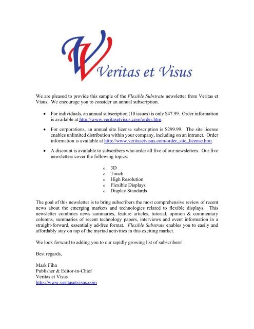
We are pleased to provide this sample of the ... - Veritas et Visus
We are pleased to provide this sample of the ... - Veritas et Visus
We are pleased to provide this sample of the ... - Veritas et Visus

Create successful ePaper yourself
Turn your PDF publications into a flip-book with our unique Google optimized e-Paper software.
<strong>We</strong> <strong>are</strong> <strong>pleased</strong> <strong>to</strong> <strong>provide</strong> <strong>this</strong> <strong>sample</strong> <strong>of</strong> <strong>the</strong> Flexible Substrate newsl<strong>et</strong>ter from <strong>Veritas</strong> <strong>et</strong><br />
<strong>Visus</strong>. <strong>We</strong> encourage you <strong>to</strong> consider an annual subscription.<br />
• For individuals, an annual subscription (10 issues) is only $47.99. Order information<br />
is available at http://www.veritas<strong>et</strong>visus.com/order.htm.<br />
• For corporations, an annual site license subscription is $299.99. The site license<br />
enables unlimited distribution within your company, including on an intran<strong>et</strong>. Order<br />
information is available at http://www.veritas<strong>et</strong>visus.com/order_site_license.htm.<br />
• A discount is available <strong>to</strong> subscribers who order all five <strong>of</strong> our newsl<strong>et</strong>ters. Our five<br />
newsl<strong>et</strong>ters cover <strong>the</strong> following <strong>to</strong>pics:<br />
ο 3D<br />
ο Touch<br />
ο High Resolution<br />
ο Flexible Displays<br />
ο Display Standards<br />
The goal <strong>of</strong> <strong>this</strong> newsl<strong>et</strong>ter is <strong>to</strong> bring subscribers <strong>the</strong> most comprehensive review <strong>of</strong> recent<br />
news about <strong>the</strong> emerging mark<strong>et</strong>s and technologies related <strong>to</strong> flexible displays. This<br />
newsl<strong>et</strong>ter combines news summaries, feature articles, tu<strong>to</strong>rial, opinion & commentary<br />
columns, summaries <strong>of</strong> recent technology papers, interviews and event information in a<br />
straight-forward, essentially ad-free format. Flexible Substrate enables you <strong>to</strong> easily and<br />
affordably stay on <strong>to</strong>p <strong>of</strong> <strong>the</strong> myriad activities in <strong>this</strong> exciting mark<strong>et</strong>.<br />
<strong>We</strong> look forward <strong>to</strong> adding you <strong>to</strong> our rapidly growing list <strong>of</strong> subscribers!<br />
Best regards,<br />
Mark Fihn<br />
Publisher & Edi<strong>to</strong>r-in-Chief<br />
<strong>Veritas</strong> <strong>et</strong> <strong>Visus</strong><br />
http://www.veritas<strong>et</strong>visus.com
Flexible Substrate<br />
<strong>Veritas</strong> <strong>et</strong> <strong>Visus</strong> Oc<strong>to</strong>ber 2007 Vol 3 No 5<br />
Hussein Chalayan, p7 Sharp, p15 Kent Displays, p43 Cornell University, p11<br />
L<strong>et</strong>ter from <strong>the</strong> publisher: There’s Indium in <strong>the</strong>m ‘thar hills… by Mark Fihn 2<br />
News from around <strong>the</strong> world 4<br />
Organic Electronics Conference and Exhibition 2007, September 24-26, Frankfurt, Germany 29<br />
Phillip Hill covers <strong>this</strong> Cintelliq organized event with presentations from ITRI, National Chung Hsing University,<br />
National Tsing-Hua University, SAIT, Bingham<strong>to</strong>n University, and Tosoh Corporation<br />
Flex-Str<strong>et</strong>ch Electronic Workshop, September 7-9, Leuven, Belgium 33<br />
Mark Fihn covers presentations from Freudenberg/IMEC/TFCG Microsystems, SiliconPipe/Verdant Electronics,<br />
Freudenberg NOK Mechatronics, Nippon Mektron/FFD, Fraunh<strong>of</strong>er IZM, and Hightec<br />
Flexible Displays 2007, June 19-21, Oakland, California 38<br />
In <strong>this</strong> second <strong>of</strong> three reports from <strong>the</strong> Intertech/PIRA-organized conference, Phillip Hill covers presentations<br />
from ipCapital Group, Honeywell, Arizona State University, Palo Al<strong>to</strong> Research Center, and Innos<br />
Soci<strong>et</strong>y for Information Display 2007 Symposium, May 20-25, Long Beach, California 43<br />
Flexible displays were high on <strong>the</strong> agenda at SID <strong>this</strong> year with around 50 papers spread across a dozen<br />
sessions. In <strong>this</strong> third report, Phillip Hill covers presentations from Kent Displays, Hong Kong University <strong>of</strong><br />
Science and Technology/Dainippon Ink and Chemicals, Corning, DuPont, and ITRI/ Cheng Kung University<br />
Smart Fabrics 2007, May 7-9, Washing<strong>to</strong>n DC 48<br />
In <strong>this</strong> third report from <strong>the</strong> Intertech/PIRA-organized event, Mark Fihn covers presentations from<br />
JFMagic/Exmovere, Philips, Textronics, Milliken, Interactive <strong>We</strong>ar, Future Shape and Foster-Miller<br />
Industry Forum on Plastics Electronics, April 24, Chicago, Illinois 51<br />
Phillip Hill’s third report on <strong>this</strong> one-day conference on printed electronics covers presentations from GSI<br />
Technologies, Add-Vision, Op<strong>to</strong>mec, Honeywell, Novalia, and Polyera<br />
Printed Electronics Europe 2007, April 17-18, Cambridge, UK 55<br />
In <strong>this</strong> second <strong>of</strong> three reports on <strong>the</strong> IDTechEx-organized event, Phillip Hill covers presentations from<br />
Arizona State University, Aveso, Enfucell, Kodak, and Leeds Lithium Power Limited<br />
The Flexible Substrate is focused on bringing news and commentary about <strong>the</strong> activities <strong>of</strong> <strong>the</strong> companies and<br />
technologies related <strong>to</strong> <strong>the</strong> development <strong>of</strong> flexible substrates for <strong>the</strong> displays industry. The Flexible Substrate is<br />
published electronically 10 times annually by <strong>Veritas</strong> <strong>et</strong> <strong>Visus</strong>, 3305 Chelsea Place, Temple, Texas, USA, 76502.<br />
Phone: +1 254 791 0603. http://www.veritas<strong>et</strong>visus.com<br />
Publisher & Edi<strong>to</strong>r-in-Chief Mark Fihn mark@veritas<strong>et</strong>visus.com<br />
Managing Edi<strong>to</strong>r Phillip Hill phill@veritas<strong>et</strong>visus.com<br />
Associate Edi<strong>to</strong>r Ge<strong>of</strong>f Walker ge<strong>of</strong>f@verita<strong>et</strong>visus.com<br />
Contribu<strong>to</strong>rs: Lawrence Gasman, P<strong>et</strong>er Harrop, David Lieberman, Jutta Rasp, Bart<br />
Vandevelde, Chris Williams<br />
Subscription rate: US$47.99 annually. Single issues: US$7.99 each. Hard copy subscriptions <strong>are</strong> available upon<br />
request, at a rate based on location and mailing m<strong>et</strong>hod. Copyright 2007 by <strong>Veritas</strong> <strong>et</strong> <strong>Visus</strong>. All rights reserved.<br />
<strong>Veritas</strong> <strong>et</strong> <strong>Visus</strong> disclaims any propri<strong>et</strong>ary interest in <strong>the</strong> trade marks or names <strong>of</strong> o<strong>the</strong>rs.
<strong>Veritas</strong> <strong>et</strong> <strong>Visus</strong> Flexible Substrate Oc<strong>to</strong>ber 2007<br />
Ghim <strong>We</strong>i Ho, p4 JFMagic, p48 Discovery Museum, p25 FDC, p55<br />
Interview with Craig Cruikshank from cintelliq 59<br />
Interview with Adam Laubach from GSI 63<br />
Interview with Mike Thwaites from Plasma Quest 66<br />
The huge impact <strong>of</strong> printed transis<strong>to</strong>rs by P<strong>et</strong>er Harrop 70<br />
Silicon inks for electronics by Lawrence Gasman 72<br />
ILEDs: Placeholders for OLED lamps? by David Lieberman 74<br />
Smart Technology – Smart OLED – Smart Content? by Jutta Rasp 76<br />
The Last Word: Bring on November! by Chris Williams 77<br />
Display Industry Calendar 78<br />
>>>>>>>>>>>>>>>>>>>>
<strong>Veritas</strong> <strong>et</strong> <strong>Visus</strong> Flexible Substrate Oc<strong>to</strong>ber 2007<br />
recent concerns about scarce supplies <strong>of</strong> ITO, I figured <strong>the</strong>re would suddenly be a huge clamor <strong>to</strong> fully develop<br />
<strong>the</strong>se alternative technologies. But it doesn’t seem <strong>to</strong> be <strong>the</strong> case. Several LCD manufacturers have advised me that<br />
<strong>of</strong> course <strong>the</strong>y <strong>are</strong> looking at alternative technologies, but that ITO performance has not y<strong>et</strong> been equaled, and even<br />
with a 10-fold increase in ITO pricing, since very little ITO is actually used per LCD, it’s inconsequential.<br />
Brian O’Neill, who is <strong>the</strong> indium materials manager at AIM Specialty, a company that makes sputter targ<strong>et</strong>s, was<br />
very helpful in explaining <strong>the</strong> dynamics <strong>of</strong> <strong>the</strong> indium mark<strong>et</strong>. He identified several fac<strong>to</strong>rs that influence indium<br />
pricing:<br />
• Indium is a thinly-traded m<strong>et</strong>al, such that pricing can be very volatile. News about a single mine, or<br />
manipulative efforts by a single trader can heavily influence short term pricing.<br />
• Indium is a by-product <strong>of</strong> zinc mining. If zinc demand goes down, <strong>the</strong>n <strong>the</strong> supply <strong>of</strong> indium drops.<br />
• There is no economic sense <strong>to</strong> mining indium – it is a “minor element” – and dependent on <strong>the</strong> fate <strong>of</strong><br />
zinc mining. So, a couple<br />
years ago, when a French<br />
zinc mine closed, one <strong>of</strong> <strong>the</strong><br />
consequences was a rapid<br />
increase in <strong>the</strong> price <strong>of</strong><br />
indium. Today, however,<br />
Indium pricing: 1995 – July 2007<br />
demand for zinc is<br />
climbing; hence <strong>the</strong> price <strong>of</strong><br />
indium is dropping.<br />
I suggested <strong>to</strong> Brian that I’d read<br />
reports that <strong>the</strong> earth’s supply <strong>of</strong><br />
indium was likely <strong>to</strong> run out in a<br />
few years, <strong>to</strong> which he quickly<br />
advised that <strong>the</strong>re is plenty <strong>of</strong><br />
supply still in <strong>the</strong> ground. “The<br />
Brian O’Neill, AIM Specialty Materials<br />
<strong>to</strong>tal global supply <strong>of</strong> indium is similar <strong>to</strong> that <strong>of</strong> silver. <strong>We</strong>’ve been mining silver for centuries, but we’ve only<br />
been using indium for past two or three decades. Quite simply, indium is not a scarce r<strong>are</strong> m<strong>et</strong>al, and <strong>the</strong>re is<br />
nothing <strong>to</strong> suggest that we <strong>are</strong> going <strong>to</strong> run out”… He went on <strong>to</strong> explain:<br />
• There’s currently more indium wasted than is produced.<br />
• ITO sputter targ<strong>et</strong>s, for example, currently have very low utilization rates, (less than 35%).<br />
• As a result, <strong>the</strong> current mark<strong>et</strong> is an upside-down mark<strong>et</strong> – more indium is currently made from recycled<br />
material than is mined from <strong>the</strong> ground.<br />
• And considering that zinc has been mined for centuries, <strong>the</strong>re <strong>are</strong> huge amounts <strong>of</strong> indium available by<br />
simply recycling <strong>the</strong> waste from previous zinc mining.<br />
• Moreover, relatively few <strong>of</strong> <strong>the</strong> zinc producers <strong>to</strong>day even bo<strong>the</strong>r <strong>to</strong> extract indium.<br />
• And <strong>to</strong> date, <strong>the</strong>re has been very little effort <strong>to</strong> really go out and find additional sources <strong>of</strong> indium.<br />
Bot<strong>to</strong>m line, we’re not going <strong>to</strong> run out <strong>of</strong> indium any time soon. Gold prospec<strong>to</strong>rs for centuries (and again <strong>to</strong>day)<br />
have held high hopes that m<strong>et</strong>al prices would stay high and that <strong>the</strong>y would find <strong>the</strong> mo<strong>the</strong>r lode. But as prices<br />
increase, new ways <strong>to</strong> g<strong>et</strong> precious m<strong>et</strong>als <strong>are</strong> developed, and <strong>the</strong> prices drop. The same will be true for indium.<br />
While <strong>the</strong>re may be many good reasons <strong>to</strong> develop alternatives <strong>to</strong> ITO in <strong>the</strong> displays industry that <strong>are</strong> related <strong>to</strong><br />
performance, it seems unlikely that supply/demand fac<strong>to</strong>rs will play a long-term role in driving demand for<br />
alternative transp<strong>are</strong>nt electrodes. So, despite <strong>the</strong> recent hype, unless such alternative technologies really <strong>of</strong>fer<br />
improved transp<strong>are</strong>ncy, she<strong>et</strong> resistivity, flexibility, or manufacturability, or som<strong>et</strong>hing else, it seems that ITO is<br />
likely <strong>to</strong> be <strong>the</strong> dominant technology used in most display technologies for <strong>the</strong> foreseeable future…<br />
http://www.veritas<strong>et</strong>visus.com 3
<strong>Veritas</strong> <strong>et</strong> <strong>Visus</strong> Flexible Substrate Oc<strong>to</strong>ber 2007<br />
News from around <strong>the</strong> world<br />
compiled by Phillip Hill and Mark Fihn<br />
Just for fun…<br />
OK. These fascinating images <strong>are</strong>n’t really related <strong>to</strong> flexible substrates, but might spark some thoughts<br />
never<strong>the</strong>less. As creative people do more and more with organic electronics and lighting effects, it’s quickly<br />
recognizable that humanity still has a long, unknown creative genius in front <strong>of</strong> us.<br />
On <strong>the</strong> left, obviously, is an “organic keyboard”, which will no doubt blossom in<strong>to</strong> som<strong>et</strong>hing b<strong>et</strong>ter than <strong>the</strong> NTSC<br />
color gamut... On <strong>the</strong> right is a novel nano-structure fabricated by Ph.D. student Ghim <strong>We</strong>i Ho, whose Ph.D. is<br />
focused on understanding <strong>the</strong> potential device aspects <strong>of</strong> extraordinary structures like <strong>this</strong> one.<br />
On <strong>the</strong> left is <strong>the</strong> stunning “Mirror Ball”, a sculpture by artist Michael Trainor, a lighting show in Blackpool,<br />
England that lasts approximately 15 minutes as a backdrop for special events. The light show is comprised <strong>of</strong> not just<br />
<strong>the</strong> Mirror Ball but also <strong>the</strong> surrounding pedestrian <strong>are</strong>as, enabling a high level <strong>of</strong> interaction with public. The light<br />
show incorporates six moving headlights that would normally only be found indoors within nightclub environments<br />
and stage shows. On <strong>the</strong> right, Eric Darnell designed a boomerang embedded with LEDs that not only can be used at<br />
night, but enables some amazing pho<strong>to</strong> opportunities.<br />
http://www.veritas<strong>et</strong>visus.com 4
<strong>Veritas</strong> <strong>et</strong> <strong>Visus</strong> Flexible Substrate Oc<strong>to</strong>ber 2007<br />
LumiGram adds <strong>to</strong> luminous clothing line<br />
France-based LumiGram recently introduced several new cus<strong>to</strong>m clothing products based on <strong>the</strong>ir specialty<br />
luminous fabric. The technology weaves plastic optical fibers alongside syn<strong>the</strong>tic fibers, forming a luminous fabric<br />
without cus<strong>to</strong>mary problems <strong>of</strong> heat and electricity. Power comes from traditional batteries (rechargeable or<br />
disposable) or AC adapter plugged in<strong>to</strong> <strong>the</strong> wall. Unlike standard optical fibers, <strong>the</strong> fiber optic fabric emits light<br />
along <strong>the</strong> full length <strong>of</strong> <strong>the</strong> fibers. While several colors <strong>are</strong> available, <strong>the</strong> most common and <strong>the</strong> most luminous<br />
colors <strong>are</strong> blue, red, green and white). The luminous fabric can be hand washed with water up <strong>to</strong> 70°C and natural<br />
soap (<strong>the</strong> battery must be removed prior <strong>to</strong> washing). While several colors <strong>are</strong> available, <strong>the</strong> most common and <strong>the</strong><br />
most luminous colors <strong>are</strong> blue, red, green and white). In addition <strong>to</strong> clothing, LumiGram’s products include<br />
pillows, tablecloths, and accessories. http://www.lumigram.com<br />
http://www.veritas<strong>et</strong>visus.com 5
<strong>Veritas</strong> <strong>et</strong> <strong>Visus</strong> Flexible Substrate Oc<strong>to</strong>ber 2007<br />
Flash<strong>We</strong>ar develops sensor-based T-shirts<br />
A number <strong>of</strong> T-shirts have been introduced recently with electroluminescent panels that react <strong>to</strong> <strong>the</strong> environment in<br />
some way or ano<strong>the</strong>r. The T-Qualizer shirts <strong>are</strong> now available in a vari<strong>et</strong>y <strong>of</strong> styles, with an embedded graphic<br />
equalizer that reacts <strong>to</strong> <strong>the</strong> noises around it. The flexible EL panel reacts <strong>to</strong> an audio sensor and <strong>the</strong>n flashes in<br />
multiple colors <strong>to</strong> <strong>the</strong> beat <strong>of</strong> <strong>the</strong> music. Flash<strong>We</strong>ar recently introduced a woman’s version <strong>of</strong> <strong>the</strong> T-Qualizer with a<br />
heart-shaped equalizer. A somewhat different approach was recently introduced by ThinkGeek, called <strong>the</strong> WiFi<br />
D<strong>et</strong>ec<strong>to</strong>r, in which <strong>the</strong> EL panel reacts <strong>to</strong> <strong>the</strong> strength <strong>of</strong> nearby WiFi hot spots. The glowing bars on <strong>the</strong> front <strong>of</strong><br />
<strong>the</strong> shirt dynamically change as <strong>the</strong> surrounding WiFi signal strength fluctuates. The shirts all run on four AAA<br />
batteries that <strong>are</strong> hidden in an inside pock<strong>et</strong>. The T-Qualizer shirts <strong>are</strong> available for about $39, while ThinkGeek is<br />
promoting <strong>the</strong> WiFi D<strong>et</strong>ec<strong>to</strong>r Shirt for $29.99. For washing, <strong>the</strong> panels <strong>are</strong> removable. http://www.flashwear.com<br />
Picard introduces solar travel bags<br />
Picard, a Germany-based high-end bag company recently launched <strong>the</strong>ir Fall/Winter 2007 bag collection including<br />
three models with solar-power charging functionality for <strong>the</strong> environmentally-minded traveler. The solar panels<br />
charge an integrated lithium ion battery that charges <strong>to</strong> 4500mAh, enough <strong>to</strong> charge a notebook PC. Unfortunately,<br />
<strong>the</strong> conversion fac<strong>to</strong>r is not so good, as a full charge requires about 21 hours in <strong>the</strong> sun. The battery can be charged<br />
in about 5 hours via a car adapter. Picard charges a hefty fee for <strong>the</strong> feature - <strong>the</strong> Picard Solar Messenger and<br />
Business Backpack goes for $1,100 and <strong>the</strong> Solar Trolley for $1,375. http://www.marc-picard.de<br />
http://www.veritas<strong>et</strong>visus.com 6
<strong>Veritas</strong> <strong>et</strong> <strong>Visus</strong> Flexible Substrate Oc<strong>to</strong>ber 2007<br />
Hussein Chalayan designs Sparkling Crystal Dress<br />
In early Oc<strong>to</strong>ber, Hussein Chalayan surprised <strong>the</strong> audience at <strong>the</strong> Paris Fashion <strong>We</strong>ek with a showing <strong>of</strong><br />
“Technology Me<strong>et</strong>s High Fashion”, showcasing a Sparkling Crystal Dress. Ra<strong>the</strong>r than featuring models on <strong>the</strong><br />
runway, however, Chalayan bent <strong>the</strong> rules by airing a short movie. The Crystal Dress uses hundreds <strong>of</strong> servo mo<strong>to</strong>r<br />
driven tiny lasers diodes. The laser diodes <strong>are</strong> integrated in<strong>to</strong> <strong>the</strong> garments, illuminating strategically positioned<br />
Swarovski crystals, not only as part <strong>of</strong> <strong>the</strong> garment, but also <strong>the</strong>n extending <strong>the</strong> light beam beyond <strong>the</strong> dress in<strong>to</strong><br />
space. The effect is an explosion <strong>of</strong> laser beams and light effects <strong>the</strong> make <strong>the</strong> crystal look like “living, flowing<br />
lava”. Moritz Waldemeyer was <strong>the</strong> technical crea<strong>to</strong>r <strong>of</strong> <strong>the</strong> dress. One reviewer wrote, “The result is a stunning<br />
light/laser show radiated from <strong>the</strong> dress that changes continuously <strong>the</strong> light effects and reflections with <strong>the</strong><br />
movement <strong>of</strong> <strong>the</strong> we<strong>are</strong>r <strong>of</strong> <strong>the</strong> dress.” http://www.husseinchalayan.com<br />
A collaboration b<strong>et</strong>ween designer Hussein Chalayan and technology guru Moritz Waldemeyer resulted in <strong>the</strong><br />
Sparkling Crystal Dress. A video about <strong>the</strong> creation <strong>of</strong> <strong>the</strong> dress can be seen at:<br />
http://www.swarovskisparkles.tv/video/fashion/spring-summer-08/paris/hussein-chalayan-making/<br />
Hui-Zong Chen shows <strong>of</strong>f concept digital yoga mat<br />
The Yanko Design Group recently showed <strong>of</strong>f an<br />
intriguing concept from Hui-Zong Chen. Chen developed<br />
a conceptual digital yoga mat with speakers and<br />
streaming video. The idea behind <strong>this</strong> combination <strong>of</strong><br />
technologies is so that people can attend yoga classes<br />
from anywhere, utilizing <strong>the</strong> streaming video that plays<br />
right on <strong>the</strong> mat. In <strong>the</strong>ory, <strong>the</strong> yoga enthusiasts can even<br />
video-conference with friends. One commenta<strong>to</strong>r noted a<br />
paradoxical aspect <strong>to</strong> <strong>this</strong> concept, in that it also means<br />
that it would enable users <strong>to</strong> actually exercise less by<br />
saving <strong>the</strong>mselves <strong>the</strong> effort associated with attending <strong>the</strong><br />
yoga class. http://www.yankodesign.com<br />
Color Kin<strong>et</strong>ics introduces Terrarium project in New<br />
http://www.veritas<strong>et</strong>visus.com 7
<strong>Veritas</strong> <strong>et</strong> <strong>Visus</strong> Flexible Substrate Oc<strong>to</strong>ber 2007<br />
York City<br />
Color Kin<strong>et</strong>ics, recently acquired by Philips, is showing <strong>the</strong>ir Terrarium project, a permanent, site-specific public<br />
art project that reflects <strong>the</strong> evolution <strong>of</strong> TriBeCa – a neighborhood constantly in flux. The project features a light<br />
design in <strong>the</strong> lobby <strong>of</strong> a New York City landmark building built in 1881, enabled by Color Kin<strong>et</strong>ics LED lighting<br />
systems. Shifting patterns <strong>of</strong> light radiate from an assortment <strong>of</strong> acrylic bubbles mounted on <strong>the</strong> walls. Visualized<br />
by artist Grimanesa Amorós <strong>of</strong> Amorós Studio, <strong>the</strong> installation was intended <strong>to</strong> inspire reflection. Illuminating <strong>the</strong><br />
acrylic bubbles <strong>are</strong> strands <strong>of</strong> iColor Flex SLX, a flexible LED-based strand that can generate countless colors and<br />
effects without <strong>the</strong> constraints <strong>of</strong> fixture size, shape or space. Each LED strand has 50 individually controllable tricolor<br />
nodes that <strong>are</strong> driven by Color Kin<strong>et</strong>ics propri<strong>et</strong>ary Chromasic technology, which allows each node <strong>to</strong><br />
generate over 64 billion color combinations. The strands <strong>are</strong> mounted along <strong>the</strong> wall with an acrylic bubble placed<br />
over each LED-based node. Using iPlayer 2, a multiple show s<strong>to</strong>rage and playback system, and ColorPlay, light<br />
show authoring s<strong>of</strong>tw<strong>are</strong>, Amorós was able <strong>to</strong> program <strong>the</strong> Terrarium display in a few days. The DMX-based<br />
control system, which allows simple authoring and playback, removes <strong>the</strong> time and guesswork associated with<br />
bringing intricate light shows <strong>to</strong> life. Amorós said that Terrarium will inspire <strong>the</strong> community <strong>of</strong> TriBeCa for years<br />
<strong>to</strong> come. http://www.colorkin<strong>et</strong>ics.com<br />
Yeon-shin Seung conceptualizes portable DVD player with flexible OLED<br />
Yanko Design recently showcased Yeon-shin Seung’s portable DVD player (which <strong>the</strong> design house unfortunately<br />
dubbed a “PDP”). The device is comprised <strong>of</strong> a candy-bar shape that twists open <strong>to</strong> l<strong>et</strong> you insert a DVD on one<br />
side, and <strong>to</strong> unroll a flexible OLED on <strong>the</strong> o<strong>the</strong>r. http://www.yankodesign.com<br />
http://www.veritas<strong>et</strong>visus.com 8
<strong>Veritas</strong> <strong>et</strong> <strong>Visus</strong> Flexible Substrate Oc<strong>to</strong>ber 2007<br />
FlexiDis Project shows progress with EPLaR process<br />
The website for <strong>the</strong> European FlexiDis Project is newly showing <strong>of</strong>f an image<br />
that demonstrates continued progress related <strong>to</strong> <strong>the</strong>ir ElectroPhor<strong>et</strong>ic Laser<br />
Release (EPLaR) process. The amorphous silicon TFT array was made on<br />
polyimide and glass at <strong>the</strong> Thales-LCD fac<strong>to</strong>ry near Grenoble, with laser<br />
release at Philips Applied Technologies. The OLED was deposited by CEA-<br />
LETI, thin film encapsulation by Applied Materials, and <strong>the</strong> electronics were<br />
furnished by Thomson Germany. The accompanying pho<strong>to</strong> is <strong>of</strong> an OLED<br />
flexible display made by <strong>the</strong> EPLaR process shown immediately after <strong>the</strong><br />
laser release process. www.flexidis-project.org<br />
CMO announces investments in OLED and LED subsidiaries<br />
Chi Mei Op<strong>to</strong>electronics (CMO) recently announced it will make additional investments in its OLED subsidiary<br />
Chi Mei EL Corporation (CMEL), and a newly formed LED LCD subsidiary, Chi Mei Lighting, <strong>of</strong> NT$600 and<br />
NT$595 million, respectively, according <strong>to</strong> a filing with <strong>the</strong> Taiwan S<strong>to</strong>ck Exchange. http://www.cmo.com.tw<br />
NEDO contracts OLED lighting development <strong>to</strong> Matsushita, Idemitsu, and Tazmo<br />
An independent administrative institution, <strong>the</strong> New Energy and Industrial Technology Development Organization<br />
(NEDO), contracted out <strong>the</strong> development <strong>of</strong> technology for OLED lighting as one <strong>of</strong> its fiscal 2007 projects <strong>to</strong><br />
Matsushita Electric Works Ltd., Idemitsu Kosan Co. Ltd. and Tazmo Co. Ltd. The contracted companies aim <strong>to</strong><br />
commercialize <strong>the</strong> technology by March 2010. http://www.nedo.go.jp/english<br />
MIT scientists develop Pho<strong>to</strong>nic Gel Films that hold promise for display devices<br />
Scientists from <strong>the</strong> Massachus<strong>et</strong>ts Institute <strong>of</strong> Technology recently demonstrated that by alternating layers <strong>of</strong> two<br />
different polymers – one rigid and glassy, <strong>the</strong> o<strong>the</strong>r s<strong>of</strong>t and easily swollen with liquid or vapor – <strong>the</strong>y can create<br />
pho<strong>to</strong>nic gel crystals that can be tuned <strong>to</strong> reflect light <strong>of</strong> many different colors across <strong>the</strong> visible and near-infr<strong>are</strong>d<br />
spectrum. The MIT research, reported in <strong>the</strong> Oct. 21 online issue <strong>of</strong> Nature Materials, demonstrate <strong>the</strong> degree <strong>to</strong><br />
which <strong>the</strong>se pho<strong>to</strong>nic materials <strong>are</strong> tunable through changes in <strong>the</strong> s<strong>of</strong>t layer’s thickness and index <strong>of</strong> refraction.<br />
The responsiveness <strong>of</strong> <strong>the</strong> pho<strong>to</strong>nic crystals makes <strong>the</strong>m likely candidates for active components <strong>of</strong> display, sensory<br />
or telecommunication devices. In one example, <strong>the</strong> researchers show very large, reversible optical changes by<br />
varying <strong>the</strong> salt content <strong>of</strong> a water<br />
solution in which <strong>the</strong>se films <strong>are</strong><br />
dipped. Multicolor patterns can be<br />
made by sequential coating <strong>of</strong> films,<br />
with <strong>the</strong> color <strong>of</strong> each region<br />
depending on <strong>the</strong> degree <strong>to</strong> which<br />
<strong>the</strong>ir molecules <strong>are</strong> chemically<br />
interconnected. The National Science<br />
Foundation funded <strong>the</strong> research in<br />
2003 through a three-year grant<br />
aimed at creating new nanomaterials<br />
that <strong>are</strong> tunable through magn<strong>et</strong>ic,<br />
chemical or o<strong>the</strong>r techniques.<br />
Following <strong>the</strong> discovery <strong>of</strong> intriguing<br />
new effects involving <strong>the</strong> interaction<br />
<strong>of</strong> light and sound in <strong>the</strong> materials,<br />
<strong>the</strong> grant was extended for two years<br />
through a “special creativity award.”<br />
http://www.nsf.gov<br />
MIT researchers Edwin Thomas and Joseph Walish created pho<strong>to</strong>nic gel<br />
crystals that can be tuned <strong>to</strong> emit light <strong>of</strong> different colors across <strong>the</strong> visible<br />
and near-infr<strong>are</strong>d spectrum. The responsiveness <strong>of</strong> <strong>the</strong> pho<strong>to</strong>nic crystals<br />
makes <strong>the</strong>m likely candidates for components <strong>of</strong> display, sensory or<br />
http://www.veritas<strong>et</strong>visus.com 9
<strong>Veritas</strong> <strong>et</strong> <strong>Visus</strong> Flexible Substrate Oc<strong>to</strong>ber 2007<br />
Researchers from <strong>the</strong> University <strong>of</strong> Surrey enhance polymer luminescence<br />
One solution <strong>to</strong> improve <strong>the</strong> lif<strong>et</strong>ime <strong>of</strong> organic-based solution-processable devices that has been investigated is<br />
incorporating carbon nanotubes in <strong>the</strong> polymer <strong>to</strong> form a composite. These “inorganics-in-organics” hybrid<br />
composites add many new dimensions and functionality <strong>to</strong> traditional organic films. However, <strong>the</strong> addition <strong>of</strong> <strong>the</strong><br />
carbon nanotubes typically comes at a cost. For example, in light emitting materials, <strong>the</strong> presence <strong>of</strong> <strong>the</strong> CNTs<br />
reduces <strong>the</strong> emission from <strong>the</strong> composite, due <strong>to</strong> quenching <strong>of</strong> charge carriers at <strong>the</strong> nanotubes. This quenching<br />
reduces <strong>the</strong> emission efficiency <strong>of</strong> <strong>the</strong> devices. Researchers at <strong>the</strong> Advanced Technology Institute <strong>of</strong> <strong>the</strong> University<br />
<strong>of</strong> Surrey, in collaboration with researchers from China and <strong>the</strong> USA, recently demonstrated that <strong>this</strong> quenching<br />
effect is not an unavoidable problem. In fact, <strong>the</strong>y demonstrate a 100-fold increase in <strong>the</strong> light emission from a<br />
nylon polymer <strong>sample</strong>, by incorporating multi-walled carbon nanotubes (MWCNTs). This increase in lightemission<br />
only occurred when <strong>the</strong>y acid treated <strong>the</strong> MWCNTs prior <strong>to</strong> inclusion in <strong>the</strong> polymer. They propose that<br />
<strong>this</strong> increase is due <strong>to</strong> a novel energy transfer mechanism, from <strong>the</strong> acid-damaged surface <strong>of</strong> <strong>the</strong> MWCNT <strong>to</strong> <strong>the</strong><br />
emitting sites in <strong>the</strong> polymer. In addition <strong>to</strong> <strong>the</strong> enhanced light-emission, <strong>the</strong> study also demonstrates that <strong>the</strong><br />
MWCNT produced an improvement in <strong>the</strong> stability <strong>of</strong> <strong>the</strong> polymer <strong>to</strong> light-induced degradation. Pr<strong>of</strong>essor Ravi<br />
Silva, Direc<strong>to</strong>r <strong>of</strong> <strong>the</strong> Advanced Technology Institute states: “The mere fact that now we can have a predictable<br />
organic-nanotube hybrid composite, with enhanced properties should open <strong>the</strong> door for many new applications. The<br />
enhancement in <strong>the</strong> luminescence properties bodes well a new generation <strong>of</strong> organic devices that could potentially<br />
reach commercially viable figures <strong>of</strong> merit for large-scale production. <strong>We</strong> <strong>are</strong> very excited with <strong>the</strong>se initial<br />
results.” http://www.ati.surrey.ac.uk<br />
University <strong>of</strong> Buffalo scientists deposit novel m<strong>et</strong>al oxide thin films on substrates<br />
University at Buffalo chemists have developed a novel way <strong>to</strong> grow chemically pure, zinc oxide thin films<br />
characterized by dense, bristle-like nanostructures and a new m<strong>et</strong>hod for depositing <strong>the</strong>m on temperature-sensitive<br />
substrates, including polymers, plastics and tapes. The recently published research may make possible <strong>the</strong><br />
deposition <strong>of</strong> versatile zinc oxide films on<strong>to</strong> flexible surfaces, enabling <strong>the</strong> development <strong>of</strong> more efficient solar<br />
cells, liquid-crystal displays, chemical sensors and op<strong>to</strong>electronic devices. High-quality zinc oxide thin films <strong>are</strong><br />
versatile and can be fabricated in<strong>to</strong> many shapes, including films, nanorods and nanoparticles. However, <strong>the</strong>re is a<br />
drawback: <strong>the</strong>y usually <strong>are</strong> deposited at high temperatures, which can damage or even melt <strong>the</strong> substrate <strong>the</strong>y <strong>are</strong><br />
coating. The UB researchers grow <strong>the</strong> thin films by first reacting<br />
zinc m<strong>et</strong>al and oxygen in <strong>the</strong> presence <strong>of</strong> a high power, electrical<br />
arc discharge. The m<strong>et</strong>hod <strong>the</strong>y developed, called “pulsed arc<br />
molecular beam deposition” (PAMBD), strikes a discharge<br />
b<strong>et</strong>ween two pure zinc rods. The pure zinc m<strong>et</strong>al is vaporized<br />
and reacts compl<strong>et</strong>ely with an oxygen gas pulse <strong>to</strong> create<br />
chemically zinc oxide molecules. The gaseous zinc oxide is <strong>the</strong>n<br />
sprayed through a tiny aperture, a process that results in cooling<br />
<strong>the</strong> expanding gas down <strong>to</strong> about 50 degrees Kelvin, allowing <strong>the</strong><br />
beam <strong>of</strong> now cold m<strong>et</strong>al oxides <strong>to</strong> safely coat even <strong>the</strong> most<br />
temperature-sensitive surfaces. “This is an enabling technology<br />
that will allow for <strong>the</strong> deposition <strong>of</strong> thin films on batteries, credit<br />
cards, on any flexible surface you have,” Garvey said, adding<br />
that <strong>the</strong> UB process can use any m<strong>et</strong>al and a wide array <strong>of</strong><br />
different m<strong>et</strong>al oxides can be produced easily. Since it is a pulsed<br />
technique, <strong>the</strong> thickness <strong>of</strong> <strong>the</strong> resulting films can be precisely<br />
controlled. The chemists now <strong>are</strong> working <strong>to</strong> use <strong>the</strong> thin films<br />
and <strong>the</strong> deposition technique <strong>to</strong> create nanorods and spintronic<br />
devices. http://www.buffalo.edu<br />
Chemist James Garvey from <strong>the</strong> University <strong>of</strong><br />
Buffalo has developed a way <strong>to</strong> deposit m<strong>et</strong>al<br />
oxide on<strong>to</strong> a polymeric substrate, as shown<br />
in <strong>this</strong> scanning electron microscope image,<br />
magnified 30,000 times.<br />
Cornell University researchers discover nano-device that emits light<br />
http://www.veritas<strong>et</strong>visus.com 10
<strong>Veritas</strong> <strong>et</strong> <strong>Visus</strong> Flexible Substrate Oc<strong>to</strong>ber 2007<br />
In mid-Oc<strong>to</strong>ber, nanotechnologists from Cornell University announced <strong>the</strong> discovery <strong>of</strong> a material that holds<br />
promise for producing light-emitting, flexible semiconduc<strong>to</strong>rs. An interdisciplinary team had long studied <strong>the</strong><br />
molecular semiconduc<strong>to</strong>r ru<strong>the</strong>nium tris-bipyridine. For many reasons, including its ability <strong>to</strong> allow electrons and<br />
holes (spaces where electrons were before <strong>the</strong>y moved) <strong>to</strong> pass through it easily, <strong>the</strong> material has <strong>the</strong> potential <strong>to</strong> be<br />
used for flexible light-emitting devices. Sensing, microscopy and flat-panel displays <strong>are</strong> among its possible<br />
applications. The researchers s<strong>et</strong> out <strong>to</strong><br />
understand <strong>the</strong> fundamental physics <strong>of</strong> <strong>the</strong><br />
material - that is, what happens when it<br />
encounters an electric field, both at <strong>the</strong><br />
interfaces and inside <strong>the</strong> film. By fabricating<br />
a device out <strong>of</strong> <strong>the</strong> ru<strong>the</strong>nium m<strong>et</strong>al complex<br />
that was spin-coated on<strong>to</strong> an insulating<br />
substrate with pre-patterned gold electrodes,<br />
<strong>the</strong> scientists were able <strong>to</strong> use electron force<br />
microscopy <strong>to</strong> measure directly <strong>the</strong> electric<br />
field <strong>of</strong> <strong>the</strong> device. Essential <strong>to</strong> <strong>the</strong> effort was<br />
<strong>the</strong> ability <strong>to</strong> pattern <strong>the</strong> ru<strong>the</strong>nium complex<br />
using pho<strong>to</strong>lithography, a technique not<br />
normally used with such materials and one<br />
that <strong>to</strong>ok <strong>the</strong> researchers more than three<br />
Top view <strong>of</strong> <strong>the</strong> ru<strong>the</strong>nium trisbipyridine<br />
light-emitting<br />
device created by Cornell<br />
University researchers. The<br />
ru<strong>the</strong>nium m<strong>et</strong>al complex is<br />
represented by red spheres,<br />
and counter ions <strong>are</strong><br />
represented by green spheres.<br />
The material is sandwiched<br />
b<strong>et</strong>ween two gold electrodes.<br />
Also visible is <strong>the</strong> probe <strong>of</strong> <strong>the</strong><br />
electron force microscope used<br />
<strong>to</strong> measure <strong>the</strong> electric field <strong>of</strong><br />
<strong>the</strong> device.<br />
years <strong>to</strong> perfect, using <strong>the</strong> knowledge <strong>of</strong> experts in nano-fabrication, materials, and chemistry. The patterning<br />
worked by laying down a gold electrode and a polymer called parylene. By depositing <strong>the</strong> ru<strong>the</strong>nium complex on<br />
<strong>to</strong>p <strong>of</strong> <strong>the</strong> parylene layer and filling in an <strong>et</strong>ched gap b<strong>et</strong>ween <strong>the</strong> gold electrodes, <strong>the</strong> researchers were <strong>the</strong>n able <strong>to</strong><br />
peel <strong>the</strong> parylene material <strong>of</strong>f mechanically, leaving a perfect device. http://www.cornell.edu<br />
BioFlex Project shows wireless link designed in<strong>to</strong> str<strong>et</strong>chable, submersible design<br />
In <strong>the</strong> frame <strong>of</strong> <strong>the</strong> BioFlex project, a wireless link was designed in <strong>the</strong> str<strong>et</strong>chable technology. Due <strong>to</strong> <strong>the</strong> inductive<br />
power transmission b<strong>et</strong>ween <strong>the</strong> external coil and <strong>the</strong> embedded coil, a LED is burning. This application also<br />
demonstrates <strong>the</strong> possibility <strong>to</strong> make str<strong>et</strong>chable circuits water resistant. The electronic design <strong>of</strong> <strong>the</strong> wireless link<br />
and <strong>the</strong> driving circuit was done by KULeuven ESAT-MICAS, <strong>the</strong> technology for <strong>the</strong> water resistant circuit was<br />
developed by TFCG Microsystems. http://tfcg.elis.ugent.be/projects/str<strong>et</strong>chable.html<br />
On <strong>the</strong> left is an LED-powered by inductive coil embedded in PDMS; <strong>the</strong> image on <strong>the</strong> right is <strong>the</strong> same<br />
inductive coil with <strong>the</strong> LED also embedded in <strong>the</strong> PDMS. Both devices <strong>are</strong> fully submerged.<br />
http://www.veritas<strong>et</strong>visus.com 11
<strong>Veritas</strong> <strong>et</strong> <strong>Visus</strong> Flexible Substrate Oc<strong>to</strong>ber 2007<br />
Georgia Institute <strong>of</strong> Technology develops new nanolithography technique<br />
Scientists at <strong>the</strong> Georgia Institute <strong>of</strong> Technology have developed a new technique for nanolithography that is<br />
extremely fast and capable <strong>of</strong> being used in a range <strong>of</strong> environments including air (outside a vacuum) and liquids.<br />
Researchers have demonstrated <strong>the</strong> technique, known as <strong>the</strong>rmochemical nanolithography, as a pro<strong>of</strong> <strong>of</strong> concept.<br />
The technique may allow industry <strong>to</strong> produce a vari<strong>et</strong>y <strong>of</strong> nanopatterned structures, including nanocircuits, at a<br />
speed and scale that could make <strong>the</strong>ir manufacture commercially viable. The research, which has potential<br />
applications for fields ranging from <strong>the</strong> electronics industry <strong>to</strong> nan<strong>of</strong>luidics <strong>to</strong> medicine, appe<strong>are</strong>d earlier <strong>this</strong> year<br />
in <strong>the</strong> journal Nano L<strong>et</strong>ters. Using an a<strong>to</strong>mic force microscope (AFM), researchers heat a silicon tip and run it over<br />
a thin polymer film. The heat from <strong>the</strong> tip induces a chemical reaction at <strong>the</strong> surface <strong>of</strong> <strong>the</strong> film. This reaction<br />
changes <strong>the</strong> film’s chemical reactivity and transforms it from a hydrophobic<br />
substance <strong>to</strong> a hydrophilic one that can stick <strong>to</strong> o<strong>the</strong>r molecules. The technique is<br />
extremely fast and can write at speeds faster than millim<strong>et</strong>ers per second. That’s<br />
orders <strong>of</strong> magnitude faster than <strong>the</strong> widely used dip-pen nanolithography (DPN),<br />
which routinely clocks at a speed <strong>of</strong> 0.0001 millim<strong>et</strong>ers/s. Using <strong>the</strong> new<br />
technique, researchers were able <strong>to</strong> pattern with dimensions down <strong>to</strong> 12<br />
nanom<strong>et</strong>ers in width in a vari<strong>et</strong>y <strong>of</strong> environments. O<strong>the</strong>r techniques typically<br />
require <strong>the</strong> addition <strong>of</strong> o<strong>the</strong>r chemicals <strong>to</strong> be transferred <strong>to</strong> <strong>the</strong> surface or <strong>the</strong><br />
presence <strong>of</strong> strong electric fields. TCNL doesn’t have <strong>the</strong>se requirements and can<br />
be used in humid environments outside a vacuum. By using an array <strong>of</strong> AFM tips<br />
developed by IBM, TCNL also has <strong>the</strong> potential <strong>to</strong> be massively scalable,<br />
allowing users <strong>to</strong> independently draw features with thousands <strong>of</strong> tips at a time<br />
ra<strong>the</strong>r than just one. http://www.gatech.edu<br />
The initials for <strong>the</strong> Georgia<br />
Institute <strong>of</strong> Technology written<br />
with <strong>the</strong> <strong>the</strong>rmochemical<br />
nanolithography technique.<br />
PARC develops novel sensor layers<br />
As flexible electronics find <strong>the</strong>ir way in<strong>to</strong> new applications, manufacturers <strong>are</strong> faced with problems that include<br />
high-cost processing, brittle materials, large-<strong>are</strong>a scaling and more. Active-matrix amorphous silicon image sensor<br />
arrays <strong>are</strong> <strong>the</strong> workhorses for large-<strong>are</strong>a sensor applications such as X-ray imaging. The problem is that <strong>the</strong> thicker<br />
<strong>the</strong> sensor layer is, <strong>the</strong> more susceptible it is <strong>to</strong> cracking and breaking. Currently <strong>the</strong>se arrays all <strong>are</strong> fabricated on<br />
glass, but a group <strong>of</strong> researchers at Palo Al<strong>to</strong> Research Center in California, has been working with sensor arrays<br />
fabricated by plasma-enhanced chemical-vapor deposition<br />
on glass and on flexible poly<strong>et</strong>hylene naphthalate<br />
substrates, reports Pho<strong>to</strong>nics.com. According <strong>to</strong> William S.<br />
Wong, senior member <strong>of</strong> <strong>the</strong> research staff at <strong>the</strong> center, <strong>the</strong><br />
goal was <strong>to</strong> g<strong>et</strong> <strong>the</strong> backplane <strong>to</strong> perform <strong>to</strong> specifications<br />
normally seen for high-temperature devices on glass. An<br />
added challenge was <strong>to</strong> keep <strong>the</strong> sensor’s dark current from<br />
increasing as <strong>the</strong> thickness decreased. Tse Nga Ng,<br />
postdoc<strong>to</strong>ral researcher at <strong>the</strong> center, indicated that,<br />
because thinner sensor films could lead <strong>to</strong> increased current<br />
leakage, <strong>the</strong> problem became finding a film thick enough so<br />
as not <strong>to</strong> jeopardize performance but thin enough <strong>to</strong> reduce<br />
mechanical stress. This current research is in its last year as<br />
a National Institute <strong>of</strong> Standards and Technology Advanced<br />
Technology Plan project in which <strong>the</strong> researchers worked<br />
with Varian Medical Systems <strong>of</strong> Palo Al<strong>to</strong> <strong>to</strong> develop novel sensor materials. The next step in <strong>this</strong> research is <strong>to</strong><br />
develop large-<strong>are</strong>a image sensors for cargo scanning, with <strong>the</strong> goal being <strong>to</strong> reduce <strong>the</strong> cost <strong>of</strong> large-<strong>are</strong>a panels that<br />
will be used in US ports <strong>of</strong> entry. http://www.parc.xerox.com<br />
http://www.veritas<strong>et</strong>visus.com 12
<strong>Veritas</strong> <strong>et</strong> <strong>Visus</strong> Flexible Substrate Oc<strong>to</strong>ber 2007<br />
Anvik works with UIUC <strong>to</strong> pattern ITO in fewer steps<br />
A team <strong>of</strong> researchers from <strong>the</strong> University <strong>of</strong> Illinois at Urbana-Champaign and from Anvik Corp. <strong>of</strong> Hawthorne,<br />
New York recently demonstrated a fabrication technique that inscribes patterns on<strong>to</strong> thin films <strong>of</strong> ITO in fewer<br />
steps than <strong>are</strong> typically used in traditional lithography. The group used laser-driven pho<strong>to</strong>-ablation and subsequent<br />
lift-<strong>of</strong>f <strong>of</strong> an underlying pho<strong>to</strong>resist layer <strong>to</strong> pattern<br />
<strong>the</strong> ITO. In traditional lithography, a pho<strong>to</strong>resist<br />
coating is exposed so that a desired pattern is<br />
transferred on<strong>to</strong> it. Subsequent steps involve<br />
developing and, possibly, baking <strong>the</strong> resist <strong>to</strong> remove<br />
it from unwanted <strong>are</strong>as and <strong>to</strong> prep<strong>are</strong> it for fur<strong>the</strong>r<br />
processing, <strong>et</strong>ching <strong>the</strong> underlying film not covered<br />
by <strong>the</strong> resist and <strong>the</strong>n removing <strong>the</strong> resist itself.<br />
Pho<strong>to</strong>-ablation, in contrast, requires a single step for<br />
patterning because exposure <strong>to</strong> high-energy pho<strong>to</strong>ns<br />
removes a polymer wherever <strong>the</strong> fluence is high<br />
enough. The technique has been used in a vari<strong>et</strong>y <strong>of</strong><br />
<strong>are</strong>as, but processing problems including excessive<br />
line roughness and high fluence requirements have<br />
limited its application. To address <strong>the</strong>se issues, <strong>the</strong><br />
group turned <strong>to</strong> <strong>the</strong> lift-<strong>of</strong>f technique. Here, a polymer<br />
film is freed from a substrate; <strong>the</strong> lift-<strong>of</strong>f removes <strong>the</strong><br />
film and anything on <strong>to</strong>p <strong>of</strong> it as well. The technique<br />
will be most useful for high-volume manufacturing,<br />
where <strong>the</strong> saving <strong>of</strong> several steps could have a<br />
pronounced effect. http://www.anvik.com<br />
In a novel thin-film patterning process, a resist that covers <strong>the</strong><br />
entire <strong>are</strong>a (left) is pho<strong>to</strong>-ablated with an excimer laser<br />
(middle). Indium tin oxide is <strong>the</strong>n deposited over everything.<br />
When <strong>the</strong> resist is removed via a lift-<strong>of</strong>f process, <strong>the</strong> indium<br />
tin oxide (ITO) remains where <strong>the</strong> resist had been pho<strong>to</strong>ablated<br />
(right). TFT = thin-film transis<strong>to</strong>r.<br />
NanoMark<strong>et</strong>s says silicon nano-crystal and printed silicon electronics mark<strong>et</strong>s <strong>to</strong> reach $2.5 billion by 2015<br />
A new report from NanoMark<strong>et</strong>s says that silicon nanocrystals and printed forms <strong>of</strong> silicon will transform<br />
electronics over <strong>the</strong> next decade with new memory, logic, pho<strong>to</strong>voltaic and op<strong>to</strong>electronic products enabled by <strong>this</strong><br />
new technology reaching $2.5 billion in revenue by 2015. The report states that <strong>this</strong> new silicon revolution enables<br />
flexible and large electronics for <strong>the</strong> first time, challenging <strong>the</strong> his<strong>to</strong>rical role <strong>of</strong> organic materials. Key points from<br />
<strong>the</strong> report include:<br />
• Ink j<strong>et</strong>, transfer printing and o<strong>the</strong>r forms <strong>of</strong> printing silicon <strong>are</strong> expected <strong>to</strong> bring new levels <strong>of</strong><br />
functionality and performance <strong>to</strong> printed RFID and display backplanes. Sales <strong>of</strong> printed silicon thin film<br />
transis<strong>to</strong>r products <strong>are</strong> expected <strong>to</strong> reach $1.9 billion by 2015.<br />
• The new silicon electronics and pho<strong>to</strong>nics will create important new opportunities <strong>to</strong> sell high margin<br />
nanocrystalline materials, precursors, and inks – estimated <strong>to</strong> reach $529 million by 2015.<br />
• Computer memories made with nanocrystalline silicon floating gates will be half <strong>the</strong> size <strong>of</strong><br />
conventional flash memories, use less power and cost less. Silicon nanocrystals could also serve as <strong>the</strong><br />
basis for new optical memories that could help speed up next-generation optical n<strong>et</strong>works. Revenues<br />
generated by silicon crystal enabled memories will reach approximately $260 million by 2015.<br />
• Solar panels created using nanocrystalline silicon - some <strong>of</strong> <strong>the</strong>m printed with silicon inks -- <strong>are</strong><br />
expected <strong>to</strong> <strong>of</strong>fer efficiencies higher than any current commercial pho<strong>to</strong>voltaic cells can <strong>of</strong>fer. By 2015<br />
solar panels created using <strong>this</strong> technology <strong>are</strong> expected <strong>to</strong> reach sales levels <strong>of</strong> around $245 million.<br />
Firms mentioned in <strong>the</strong> report include: Aixtron, Applied Materials, Atmel, CEA-LETI, Dow Corning, Evergreen<br />
Solar, Freescale, Innovalight, Infineon, Intel, Kovio, Luxtera, Micron, Mitsui, Mo<strong>to</strong>rola, NanoGram, Plastic Logic,<br />
Polymer Vision, Qin<strong>et</strong>iQ, Samsung, Seiko-Epson, Semprius, and United Solar Ovonic. http:///www.nanomark<strong>et</strong>s.n<strong>et</strong><br />
http://www.veritas<strong>et</strong>visus.com 13
<strong>Veritas</strong> <strong>et</strong> <strong>Visus</strong> Flexible Substrate Oc<strong>to</strong>ber 2007<br />
NanoMark<strong>et</strong>s <strong>to</strong> bring out new OPV report<br />
“Materials Mark<strong>et</strong>s for Thin-Film and Organic Pho<strong>to</strong>voltaics” is <strong>the</strong> upcoming NanoMark<strong>et</strong>s report, slated for<br />
release in Q1’08, and will cover <strong>the</strong> mark<strong>et</strong>s for materials used in thin-film and organic pho<strong>to</strong>voltaics namely,<br />
amorphous silicon, nano-silicon inks, CdTe, CIGS and a vari<strong>et</strong>y <strong>of</strong> organic polymers, dyes, <strong>et</strong>c. These materials <strong>are</strong><br />
covered in a recent study published by NanoMark<strong>et</strong>s titled “Thin-Film, Organic and Printable Pho<strong>to</strong>voltaics<br />
Mark<strong>et</strong>s: 2007-2015” that looked at <strong>the</strong> entire thin-film/organic PV mark<strong>et</strong>. However, <strong>the</strong> intent <strong>of</strong> <strong>the</strong> new report is<br />
<strong>to</strong> extend <strong>the</strong> analysis <strong>of</strong> <strong>the</strong> recent report and delve deeper in<strong>to</strong> <strong>the</strong> advantages, disadvantages, research directions,<br />
and manufacturability associated with PV materials. The report will also include pr<strong>of</strong>iles <strong>of</strong> firms involved in<br />
developing and manufacturing thin film/organic PV materials and d<strong>et</strong>ailed eight-year forecasts <strong>of</strong> <strong>the</strong> materials<br />
mark<strong>et</strong>s in value and volume terms with break outs by application and materials. http:///www.nanomark<strong>et</strong>s.n<strong>et</strong><br />
NanoMark<strong>et</strong>s brings out report on thin-film batteries<br />
NanoMark<strong>et</strong>s recently published “Thin-Film and Printed Batteries Mark<strong>et</strong>s: 2007-2014”. Many <strong>of</strong> <strong>the</strong> actual or<br />
envisioned applications for printable and organic electronics require <strong>the</strong>ir own power sources <strong>to</strong> make <strong>the</strong>m<br />
function. Cases in point include active RFID tags, point-<strong>of</strong>-purchase displays, active cosm<strong>et</strong>ic/drug delivery<br />
patches, low-cost medical diagnostic products, remote sensor arrays and smart cards. A growing number <strong>of</strong> firms<br />
<strong>are</strong> looking for thin-film batteries that can be printed. http:///www.nanomark<strong>et</strong>s.n<strong>et</strong><br />
DisplaySearch report highlights OLED pen<strong>et</strong>ration<br />
With <strong>the</strong> emergence <strong>of</strong> <strong>the</strong> highly anticipated AMOLED displays, <strong>this</strong> segment continues <strong>to</strong> develop, experiencing<br />
unit shipment growth <strong>of</strong> 4% Q/Q and 24% Y/Y, hitting <strong>the</strong> 19.8 million mark in Q2’07, according <strong>to</strong> <strong>the</strong> latest<br />
report from DisplaySearch. On a revenue basis, OLEDs hit $123.4M in Q2’07, down only 1% Q/Q and up 13%<br />
Y/Y, even as ASPs fell 9% Q/Q. Over <strong>the</strong> last year, main display shipments were up 16%, sub-displays up 77%, car<br />
audio displays up 35% and industrial displays up 295%. The report’s findings also show that AMOLED displays<br />
<strong>are</strong> beginning <strong>to</strong> impact <strong>the</strong> mark<strong>et</strong>, as Samsung SDI moves in<strong>to</strong> full production, and Chi Mei and LG begin <strong>to</strong> ship<br />
qualification units. Fur<strong>the</strong>rmore, Sony is expected <strong>to</strong> begin shipping <strong>the</strong>ir highly anticipated 11-inch AMOLED TV<br />
display in Q4’07. The <strong>to</strong>p five OLED manufacturers shown in Table 1 accounted for a combined mark<strong>et</strong> sh<strong>are</strong> <strong>of</strong><br />
85.4%. For <strong>the</strong> first time in several quarters, <strong>the</strong>re were two new entrants in <strong>the</strong> PMOLED mark<strong>et</strong>, Visionox and<br />
Truly, which <strong>are</strong> both located in China. Next quarter, MED is expected <strong>to</strong> begin production <strong>of</strong> microdisplays and<br />
will be <strong>the</strong> first OLED comp<strong>et</strong>i<strong>to</strong>r for eMagin. http://www.displaysearch.com<br />
Top Five OLED Manufacturers' Q2'07 Revenue Mark<strong>et</strong> Sh<strong>are</strong> and Growth (US$ Millions)<br />
Rank Company Q2'07 Revenue (US$M) Mark<strong>et</strong> Sh<strong>are</strong> Q/Q Growth Y/Y Growth<br />
1 Samsung SDI 33.8 27.4% 30% 50%<br />
2 Pioneer 24.7 20.0% -2% 62%<br />
3 RiTdisplay 23.0 18.6% -2% 67%<br />
4 LGE 22.7 18.4% -7% -17%<br />
5 TDK 5.6 4.5% -5% -29%<br />
O<strong>the</strong>rs 13.6 11.0% -29% -40%<br />
Total 123.4 100.0% -1% 13%<br />
Research and Mark<strong>et</strong>s brings out new report on polymer technology<br />
Research and Mark<strong>et</strong>s has announced <strong>the</strong> addition <strong>of</strong> “Advances in Polymer Technology” <strong>to</strong> <strong>the</strong>ir <strong>of</strong>fering. This<br />
report analyzes several scientific and technological advances that have been achieved and which <strong>are</strong> leading <strong>to</strong>ward<br />
new applications for plastics and advanced polymers. The report reviews important research efforts in polymer<br />
science, discusses potential commercial applications, and indicates when some potential products and processes<br />
will be commercially viable. Polymer research is in <strong>the</strong> fields <strong>of</strong> electronics, nanotechnology, substrate science,<br />
d<strong>et</strong>ection, optics and healthc<strong>are</strong>. http://www.researchandmark<strong>et</strong>s.com/reports/c71413<br />
http://www.veritas<strong>et</strong>visus.com 14
<strong>Veritas</strong> <strong>et</strong> <strong>Visus</strong> Flexible Substrate Oc<strong>to</strong>ber 2007<br />
Launch <strong>of</strong> Plastic Electronics Technology Centre website<br />
The Plastic Electronics Technology Centre (PETeC) website has been launched. PETeC is a national pro<strong>to</strong>typing<br />
institute for <strong>the</strong> development and commercialization <strong>of</strong> printed electronics. Cus<strong>to</strong>mers <strong>of</strong> <strong>the</strong> center will be able <strong>to</strong><br />
test design concepts and novel materials for a vari<strong>et</strong>y <strong>of</strong> products including thin film transis<strong>to</strong>rs (TFT) for flexible<br />
displays including e-paper, organic pho<strong>to</strong>voltaic cells (OPVs) and solid state lighting (SSL) applications.<br />
http://www.ukp<strong>et</strong>ec.com<br />
USDC opens registrations for January conference<br />
The US Display Consortium (USDC), a public/private partnership chartered with developing <strong>the</strong> flexible<br />
electronics and displays industry supply chain, opened registration for its 7th annual Flexible Electronics &<br />
Displays Conference and Exhibition. USDC announced that <strong>the</strong> 2008 conference keynote will be delivered by Dr.<br />
A. Michael Andrews, vice president <strong>of</strong> research and engineering, and chief technology <strong>of</strong>ficer, <strong>of</strong> L-3<br />
Communications Corporation. USDC has enhanced <strong>the</strong> 2008 conference with a new track <strong>of</strong> academic and<br />
fundamental research peer-reviewed presentations from universities worldwide. The conference will be held<br />
January 21–24, 2008, at <strong>the</strong> Pointe Hil<strong>to</strong>n Squaw Peak in Phoenix, Ariz. http://www.usdc.org<br />
IDTechEx expects record attendance for Printed Electronics USA 2007<br />
According <strong>to</strong> IDTechEx, with 3 weeks <strong>to</strong> <strong>the</strong> show <strong>the</strong>re over 45 confirmed exhibi<strong>to</strong>rs and more than 400 registered<br />
delegates. The targ<strong>et</strong>ed figure <strong>of</strong> 500 delegates on <strong>the</strong> day is likely <strong>to</strong> be smashed. Record attendance has been<br />
achieved by featuring world first presentations, such as from Kovio, and by focusing on <strong>the</strong> application <strong>of</strong> printed<br />
electronics, with presentations from companies such as Hasbro and Cubic Transportation Systems that have not<br />
presented on such activities before. Delegates include potential users such as Procter & Gamble, Lockheed Martin,<br />
BP, Coors Brewing and Crayola. New for 2007 will be <strong>the</strong> "Printed Electronics Products" demonstration <strong>are</strong>a,<br />
designed <strong>to</strong> show <strong>the</strong> huge range <strong>of</strong> products which <strong>are</strong> already in <strong>the</strong> mark<strong>et</strong> place. These will include everything<br />
from printed displays used already in commercial advertisement posters <strong>to</strong> commercial e-paper readers from Sony<br />
<strong>to</strong> cosm<strong>et</strong>ic skin patches from Estee Lauder - all powered <strong>to</strong>day by printed electronics. Delegates will be able <strong>to</strong> see<br />
what products <strong>are</strong> already in <strong>the</strong> mark<strong>et</strong> and how developers have achieved success - <strong>of</strong>ten by creating new<br />
mark<strong>et</strong>s. http://www.IDTechEx.com/peUSA<br />
Sharp shows <strong>of</strong>f super-thin LCD for mobile applications<br />
Sharp Corporation has successfully developed a 2.2-inch super-thin LCD for mobile devices with a thickness <strong>of</strong><br />
only 0.68 mm, <strong>the</strong> industry’s thinnest, <strong>the</strong> company says. Mobile devices such as mobile phones and digital<br />
cameras <strong>are</strong> rapidly becoming thinner as manufacturers strive <strong>to</strong> improve portability and <strong>of</strong>fer consumers more<br />
stylish designs. As a result, thinner embedded components such as LCDs <strong>are</strong> also increasing in demand. In<br />
addition, <strong>the</strong> increase in demand for One-Seg (terrestrial digital<br />
broadcast) compatible hands<strong>et</strong>s is leading <strong>to</strong> demands for greater<br />
visibility and higher image quality in displays intended for mobile<br />
devices. This new “Mobile Advanced Super View LCD” delivers<br />
superior image quality approaching that <strong>of</strong> an LCD TV thanks <strong>to</strong> a<br />
high contrast ratio <strong>of</strong> 2000:1, wide viewing angle <strong>of</strong> 176°, and fast<br />
response speed <strong>of</strong> 8 ms. http://sharp-world.com<br />
Sharp <strong>to</strong> take 14% stake in Pioneer<br />
Japanese electronics maker Sharp Corp will buy about $357 million worth <strong>of</strong> new sh<strong>are</strong>s from Pioneer Corp and<br />
work with its loss-making rival in developing DVD players, car electronics and displays, reports Reuters. The deal<br />
is <strong>the</strong> latest move by Japan’s electronics conglomerates <strong>to</strong> form alliances or ditch unpromising businesses <strong>to</strong> try and<br />
keep up with deep-pock<strong>et</strong>ed global rivals and respond <strong>to</strong> increasing sh<strong>are</strong>holder pressure for b<strong>et</strong>ter r<strong>et</strong>urns. While<br />
Sharp is one <strong>of</strong> <strong>the</strong> strong players in <strong>the</strong> fast-growing flat TV mark<strong>et</strong>, Pioneer has been losing money because it<br />
lacks <strong>the</strong> scale <strong>to</strong> make its products as efficiently as Matsushita Electric Industrial or LG Electronics.<br />
http://www.veritas<strong>et</strong>visus.com 15
<strong>Veritas</strong> <strong>et</strong> <strong>Visus</strong> Flexible Substrate Oc<strong>to</strong>ber 2007<br />
ITRI develops novel color e-book technology<br />
Taiwan’s Industrial Technology Research Institute (ITRI) Display Center developed a novel structure reflective<br />
single layer color cholesteric LCD display. Current commercialized electronic paper <strong>are</strong> mostly available in a single<br />
color, but in <strong>the</strong> past few years many manufacturers plunged in<strong>to</strong> <strong>the</strong> development <strong>of</strong> full color electronic paper<br />
display technology. Where electrophor<strong>et</strong>ic display EPD coloration has <strong>to</strong> be combined with a color filter, <strong>this</strong><br />
resulted in lower brightness and contrast ratio. The traditional full color cholesteric LCD display is stacked by three<br />
layers <strong>of</strong> monochrome cholesteric panels, for example, Fujitsu 3-layer reflective color cholesteric LCD display<br />
where structural design adopted switching and reflection <strong>of</strong> various reflective layers <strong>to</strong> reach a color effect, but such<br />
a structure has disadvantages <strong>of</strong> difficult pixel registration, increased<br />
cost <strong>of</strong> <strong>the</strong> drive system and process, and enhanced difficulty <strong>of</strong><br />
electrode design, and being not easy <strong>to</strong> bend. In order <strong>to</strong> solve <strong>the</strong>se<br />
problems, ITRI developed a novel structure reflective single layer<br />
color cholesteric LCD display, which adopted vacuum filling or inkj<strong>et</strong><br />
printing technology; red, green, blue cholesteric liquid crystals were<br />
cast in<strong>to</strong> or sprayed on <strong>the</strong> pixel structure, <strong>the</strong>n <strong>the</strong> structural package<br />
was done <strong>to</strong> realize a single layer color display. The overall thickness<br />
is more than 50% less than a traditional color cholesteric LCD display.<br />
The Specification <strong>of</strong> <strong>this</strong> technology is 10.4-inch, passive reflection,<br />
resolution <strong>of</strong> 320x240 with 512 colors and a panel thickness <strong>of</strong><br />
1.4mm. http://www.itri.org.tw<br />
Jinke Hanlin e-book device V3 uses Vizplex EPD<br />
Tianjin Jinke Electronics <strong>of</strong> China announced <strong>the</strong> worldwide launch <strong>of</strong> <strong>the</strong>ir Hanlin ebook<br />
V3 based on Vizplex e-paper technology from E Ink. The worldwide release <strong>of</strong><br />
Jinke’s V3 follows <strong>the</strong> successful worldwide launch <strong>of</strong> <strong>the</strong> V8 and V2 over <strong>the</strong> past<br />
year. The Hanlin eBook V3 <strong>of</strong>fers easy operation, low power consumption with all <strong>the</strong><br />
benefits <strong>of</strong> an electronic paper display and a weight <strong>of</strong> 220 g. The display, which<br />
utilizes Vizplex display, is 6 inches on <strong>the</strong> diagonal. The V3 will support a vari<strong>et</strong>y <strong>of</strong><br />
content services including e-books and e-magazines, as well as a wide vari<strong>et</strong>y <strong>of</strong><br />
content in common formats including PDF, DOC, WOLF, HTML, MP3, TXT, FB2,<br />
DJUV and Images. It will also support e-pub and Mobipock<strong>et</strong> formats. The V3 runs<br />
on LINUX OS, and open SDK <strong>to</strong> coopera<strong>to</strong>rs, supporting multi-language which<br />
includes English, Chinese, Russian, Ukraine, Turkish, French, Spanish, German,<br />
Bulgarian, Japanese and Korean. http://www.jinke.com.cn/english<br />
Les Echos first French electronic daily newspaper on iRex iLiad<br />
Les Echos, <strong>the</strong> French business newspaper, and iRex Technologies announced <strong>the</strong>ir cooperation in introducing <strong>the</strong><br />
Les Echos electronic paper edition on <strong>the</strong> iRex iLiad for <strong>the</strong> French mark<strong>et</strong> in September. There <strong>are</strong> two different<br />
editions: Les Echos and AFP, updated every hour (7am – 9pm) from Monday <strong>to</strong> Friday via <strong>the</strong> WiFi delivery direct<br />
in<strong>to</strong> <strong>the</strong> electronic paper device, without <strong>the</strong> need for a PC. http://www.irextechnologies.com<br />
Citala takes over Xymox Technologies’ display division<br />
Israel-based Citala recently compl<strong>et</strong>ed <strong>the</strong> acquisition <strong>of</strong> Xymox Technologies’ Display Products Division, also<br />
known as Paneltec (Sunnyvale, California). Now an integral part <strong>of</strong> Citala’s international organization, Xymox<br />
Display Products will be renamed Citala US Inc. Leveraging Citala’s versatile capabilities in <strong>the</strong> flexible display<br />
mark<strong>et</strong> with Xymox’s strengths as a cus<strong>to</strong>m designer, manufacturer and integra<strong>to</strong>r <strong>of</strong> flexible displays, <strong>this</strong><br />
acquisition will fur<strong>the</strong>r position Citala as a premium global <strong>provide</strong>r <strong>of</strong> integrated flexible display solutions. The<br />
acquisition follows a couple <strong>of</strong> years <strong>of</strong> successful cooperation b<strong>et</strong>ween <strong>the</strong> two companies in business, technology<br />
and product development. http://www.citala.com<br />
http://www.veritas<strong>et</strong>visus.com 16
<strong>Veritas</strong> <strong>et</strong> <strong>Visus</strong> Flexible Substrate Oc<strong>to</strong>ber 2007<br />
Bridges<strong>to</strong>ne shows latest electronic paper at 0.29mm thickness<br />
Nikkei reports that Bridges<strong>to</strong>ne developed a flexible color electronic paper with a thickness <strong>of</strong> only 0.29 mm. The<br />
company aims <strong>to</strong> produce it by continuous roll-<strong>to</strong>-roll processing because <strong>the</strong> e-paper employs a film substrate. The<br />
pro<strong>to</strong>type panel was not manufactured by continuous processing, but <strong>the</strong> company is reportedly focused on <strong>the</strong><br />
establishment <strong>of</strong> a roll-<strong>to</strong>-roll production system by using <strong>the</strong> equipment brought <strong>to</strong> its technical center in Kodaira,<br />
Tokyo. In May 2006, Bridges<strong>to</strong>ne unveiled a flexible e-paper, which was a two-color display unit using electronic<br />
liquid powder in two colors sealed in <strong>the</strong> device. The latest e-paper is capable <strong>of</strong> displaying 4,096 full-color with<br />
<strong>the</strong> adoption <strong>of</strong> RGBW color filters combined with <strong>the</strong> powder. The panel was on display at FPD International<br />
2007 from Oc<strong>to</strong>ber 24-26, along with <strong>the</strong> A3-size full-color e-paper unveiled at <strong>the</strong> same time.<br />
ZINK Imaging closes purchase <strong>of</strong> Konica Minolta manufacturing facility<br />
ZINK Imaging, <strong>the</strong> innova<strong>to</strong>rs behind <strong>the</strong> recently-unveiled Zero-Ink digital printing technology, <strong>of</strong>ficially<br />
compl<strong>et</strong>ed purchase <strong>of</strong> a state-<strong>of</strong>-<strong>the</strong>-art manufacturing facility from Konica Minolta Manufacturing USA<br />
(KMMU). ZINK Imaging plans <strong>to</strong> begin manufacturing its Zero-Ink paper at <strong>the</strong> North Carolina facility <strong>this</strong> year.<br />
They will also manufacture o<strong>the</strong>r digital imaging materials for OEM cus<strong>to</strong>mers. ZINK Imaging originally<br />
announced its intent <strong>to</strong> purchase <strong>the</strong> Konica Minolta facility on June 14, 2007. The plant, located in Whits<strong>et</strong>t, North<br />
Carolina, is a coating and chemical mix facility originally built in 1989 for <strong>the</strong> production <strong>of</strong> a vari<strong>et</strong>y <strong>of</strong> imaging<br />
products. ZINK Imaging plans <strong>to</strong> hire <strong>the</strong> remaining employee base <strong>of</strong> approximately 60 individuals, including <strong>the</strong><br />
senior management team. The patented ZINK paper is a material with dye crystals embedded inside and a<br />
protective polymer overcoat layer outside. Before printing, <strong>the</strong> embedded dye crystals <strong>are</strong> clear, so ZINK paper<br />
looks like regular white pho<strong>to</strong> paper. A ZINK-enabled printer uses heat <strong>to</strong> activate and colorize <strong>the</strong>se dye crystals.<br />
http://www.ZINK.com<br />
Samsung shows new 14.3-inch high resolution e-paper<br />
In late September, Samsung showed <strong>of</strong>f its new 14.3-inch flexible electronic<br />
paper. Although monochrome, at 2048x1536 pixels, <strong>the</strong> solution boasts<br />
remarkably high resolution, tripled from what <strong>the</strong> company showed in May<br />
at SID. The new e-paper is only 0.3 mm thick and weighs less <strong>the</strong>n 20 g.<br />
Samsung says it can produce <strong>the</strong> new e-paper using existing TFT LCD panel<br />
production lines without investing in new facilities. The device is based on<br />
E Ink’s electrophor<strong>et</strong>ic technology. http://www.samsung.com<br />
memsstar Technology teams with SAFC Hitech on surface coatings<br />
memsstar Technology announced that it is <strong>to</strong> enter in<strong>to</strong> a strategic alliance with SAFC Hitech <strong>to</strong> supply fully<br />
qualified memsstar SPD (surface preparation and deposition) systems with standard precursor chemical materials<br />
from SAFC Hitech for surface coatings on micro devices. The alliance b<strong>et</strong>ween <strong>the</strong> two companies, both<br />
technology leaders for advanced microstructure and materials fabrication, will b<strong>et</strong>ter service <strong>the</strong> emerging<br />
technology needs <strong>of</strong> companies involved with MEMS and nanotechnology devices, claims memsstar. Example<br />
applications include micr<strong>of</strong>luidics <strong>to</strong> ensure hydrophobic or hydrophilic surface properties for devices such as<br />
inkj<strong>et</strong>s or micro-needles, and medical applications where bio-compatibility is essential. O<strong>the</strong>r applications such as<br />
moisture barriers or anti-stiction properties <strong>are</strong> required by moving micro-sensors. http://www.memsstar.com<br />
Sunic System and Novaled in joint development on thin film encapsulation<br />
Sunic System, a producer <strong>of</strong> vacuum deposition equipment for OLED, and Novaled, a <strong>provide</strong>r <strong>of</strong> doping<br />
technology and materials for organic electronics, announced a joint development. Both partners will work <strong>to</strong>ge<strong>the</strong>r<br />
<strong>to</strong> build up <strong>the</strong> next generation <strong>of</strong> thin film encapsulation (TFE) <strong>to</strong>ols, technologies and materials. Novaled and<br />
Sunic System will develop a new generation <strong>of</strong> deposition <strong>to</strong>ols and organic materials <strong>to</strong> improve <strong>the</strong> deposition<br />
process and lif<strong>et</strong>ime <strong>of</strong> TFE. http://www.novaled.com<br />
http://www.veritas<strong>et</strong>visus.com 17
<strong>Veritas</strong> <strong>et</strong> <strong>Visus</strong> Flexible Substrate Oc<strong>to</strong>ber 2007<br />
Vitex sells thin-film encapsulation system <strong>to</strong> major Japanese company<br />
On Oc<strong>to</strong>ber 22, Vitex Systems announced that its equipment licensee, Advanced Neotech Systems (ANS) <strong>of</strong> Korea,<br />
secured a purchase order for its Guardian thin-film encapsulation system from a major Japanese cus<strong>to</strong>mer.<br />
Commenting on its successes, Chyi-Shan Suen, direc<strong>to</strong>r <strong>of</strong> sales and mark<strong>et</strong>ing for Vitex, said, “ANS delivered <strong>the</strong><br />
first Guardian thin-film encapsulation system <strong>to</strong> Samsung SDI in 2005. ANS again successfully delivered <strong>the</strong><br />
Guardian system <strong>to</strong> MicroEmissive Displays (MED) for <strong>the</strong>ir production line. <strong>We</strong> <strong>are</strong> <strong>pleased</strong> with <strong>this</strong> latest<br />
vic<strong>to</strong>ry, which is a signal that thin-film encapsulation continues <strong>to</strong> gain broader adoption within <strong>the</strong> OLED<br />
industry.” http://www.ansinc.co.kr http://www.vitexsys.com<br />
Vitex Systems signs licensing agreement with Sunic System for its thin-film encapsulation system<br />
Vitex Systems announced that it has signed a licensing agreement with Sunic System <strong>of</strong> Korea. The agreement<br />
includes a technology transfer package from Vitex <strong>to</strong> Sunic, and gives Sunic <strong>the</strong> non-exclusive rights <strong>to</strong> make and<br />
sell Guardian thin-film encapsulation systems, which can be used <strong>to</strong> encapsulate various electronic components and<br />
devices, including OLED displays, thin film solar cells and thin film batteries. While <strong>the</strong> financial terms <strong>of</strong><br />
agreement were not disclosed, <strong>the</strong> license includes an upfront fee and on-going royalty payments based on <strong>to</strong>ol<br />
sales. http://www.sunic.co.kr<br />
ArcelorMittal and Novaled <strong>to</strong> intensify flexible foil collaboration<br />
ArcelorMittal, <strong>the</strong> world’s largest quality steel maker, and Novaled, OLED technology and material <strong>provide</strong>r, have<br />
joined forces for a new OLED project. The partners have developing <strong>to</strong>p-emitting OLEDs on flexible substrates for<br />
signage and lighting purposes since 2006. By using ArcelorMittal’s steel plates as substrates, remarkable properties<br />
for bendable OLED applications can be achieved. In <strong>this</strong> new collaboration Novaled contributes both its broad<br />
technical experience with respect <strong>to</strong> highly efficient and stable OLED device architectures as well as its material<br />
know-how for doped transport layers. RGB OLEDs have been processed directly on classical steel plates. The<br />
striking results showed that <strong>the</strong> Novaled technology enables standard steel foil acting as a reflective bot<strong>to</strong>m<br />
electrode. http://www.novaled.com<br />
Leadis upgrades <strong>the</strong>ir AMOLED technology and IP<br />
In late Oc<strong>to</strong>ber, Leadis announced a strategic partnership with VP Dynamics on RGBW technology for small and<br />
medium mobile displays. Leadis will license VP Dynamics' VPW RGBW technology for use in LCD, AM-OLED<br />
and o<strong>the</strong>r display drivers, empowering products with lower power consumption, higher resolution, b<strong>et</strong>ter<br />
brightness, and b<strong>et</strong>ter contrast.<br />
In a separate announcement, Leadis advised <strong>the</strong> acquisition <strong>of</strong> intellectual property from Nuelight Corporation<br />
designed <strong>to</strong> correct image sticking issues that can occur with <strong>the</strong> display <strong>of</strong> static content and significantly improve<br />
manufacturing yields in AM-OLED displays. This technology has <strong>the</strong> potential <strong>to</strong> accelerate AM-OLED mark<strong>et</strong><br />
sh<strong>are</strong> gains by making it more like <strong>the</strong> visual experience and low-power advantages <strong>of</strong>fered with AM-OLED<br />
displays. http://www.leadis.com<br />
MED begins volume production <strong>of</strong> polymer OLED microdisplays<br />
MicroEmissive Displays (MED) commenced volume production and commercial shipment <strong>of</strong> its polymer-based<br />
OLED microdisplays. It is also an important miles<strong>to</strong>ne for Vitex in its effort <strong>to</strong>ward full-fledged commercialization<br />
<strong>of</strong> OLED displays leveraging <strong>the</strong> company’s propri<strong>et</strong>ary Barix thin-film encapsulation and Barix resin system<br />
material. John McEachran, direc<strong>to</strong>r <strong>of</strong> operations for MED, noted: “The thin-film encapsulation process technology<br />
<strong>provide</strong>d by Vitex has allowed our company <strong>to</strong> take full advantage <strong>of</strong> our unique polymer OLED microdisplay<br />
design. Our eyescreen product packs 76,800 pixels on a tiny, 6mm diagonal, silicon chip but delivers our cus<strong>to</strong>mers<br />
a superior viewing experience. <strong>We</strong> <strong>are</strong> <strong>pleased</strong> <strong>to</strong> be working with both Vitex and its partner, ANS. The leadingedge<br />
encapsulation technology from Vitex and excellent support surrounding ANS’s production equipment enabled<br />
us <strong>to</strong> me<strong>et</strong> our aggressive production ramp goals.” http://www.microemissive.com<br />
http://www.veritas<strong>et</strong>visus.com 18
<strong>Veritas</strong> <strong>et</strong> <strong>Visus</strong> Flexible Substrate Oc<strong>to</strong>ber 2007<br />
eMagin announces new 3DS OLED-XL microdisplay<br />
eMagin expects <strong>to</strong> begin shipping its 3DS OLED-XL microdisplay (800x600 pixels) in <strong>the</strong> first quarter <strong>of</strong> 2008.<br />
The microdisplay <strong>of</strong>fers both analog and digital signal processing in a 0.44-inch display. This high-density OLEDon-silicon<br />
microdisplay promises an affordable, easy-<strong>to</strong>-integrate solution for many virtual imaging systems.<br />
Specific improvements include increased pixel uniformity, improved color gamut, on-chip temperature sensor and<br />
compensation, and compatibility with both analog RGB and digital video signals. http://www.emagin.com<br />
CMEL <strong>to</strong> expand OLED production<br />
Chi Mei EL Corporation (CMEL), a subsidiary <strong>of</strong> Chi Mei Op<strong>to</strong>electronics (CMO), announced that <strong>the</strong> company<br />
will invest NT$1 billion (US$30.6 million) <strong>to</strong> expand <strong>to</strong> a second OLED production line. Volume production is<br />
slated for 2008, said CMO president Chao-Yang Ho. The second line will house a monthly capacity <strong>of</strong> 700,000 2inch<br />
equivalent panels. Additionally, CMEL will introduce a 7.6-inch OLED in <strong>the</strong> second quarter, and when <strong>the</strong><br />
second OLED production line starts operation, CMEL intends <strong>to</strong> introduce 11- and 12-inch panels and expects <strong>to</strong><br />
<strong>of</strong>fer 32-inch AMOLED panels during 2010. The company exhibited a 25-inch AMOLED panel at <strong>the</strong> FPD<br />
International 2007 in Japan in late Oc<strong>to</strong>ber. http://www.cmel.com.tw<br />
Samsung SDI develops ultra-thin OLED panel with 0.25-mm thickness<br />
Samsung SDI developed an ultra-thin OLED panel with a thickness <strong>of</strong> 0.25 mm. The product thickness <strong>of</strong> 0.25 mm<br />
is <strong>the</strong> <strong>to</strong>tal thickness for <strong>the</strong> panel and deflecting plate, enabled by <strong>the</strong> use <strong>of</strong> a 0.05 mm glass substrate, which is<br />
thinner than pho<strong>to</strong>graphic film. The 4.0-inch ultra-thin OLED pro<strong>to</strong>type features a resolution <strong>of</strong> 480x272 pixels.<br />
The panel can be bent slightly as a result <strong>of</strong> its thinness. According <strong>to</strong> <strong>the</strong> company, <strong>the</strong> pro<strong>to</strong>type panel can<br />
reproduce 16.7 million colors, 100% <strong>of</strong> <strong>the</strong> NTSC color gamut, a luminance <strong>of</strong> 200 cd/m 2 , a contrast ratio <strong>of</strong><br />
1,000:1 and a service life <strong>of</strong> 20,000 hours. Low-temperature poly-silicon liquid crystal is used for <strong>the</strong> TFT<br />
backplane. The OLED device is made <strong>of</strong> low-molecular material using a <strong>to</strong>p-emission structure.<br />
The slimness <strong>of</strong> <strong>the</strong> 0.25 mm panel allows it <strong>to</strong> be bent. The image on <strong>the</strong> right shows <strong>the</strong> glass substrate,<br />
which measures only 0.05 mm. Next <strong>to</strong> it is a 0.12 mm pho<strong>to</strong>graphic film – although <strong>the</strong> comparison<br />
indicates <strong>the</strong> relative rigidity <strong>of</strong> <strong>the</strong> glass substrate…<br />
Samsung shows 14-inch OLED TV<br />
Samsung Electronics showed three pro<strong>to</strong>type TVs based on 14-inch OLED panels at <strong>the</strong> FPD Expo in Yokohama in<br />
late Oc<strong>to</strong>ber. Samsung’s OLED screens were designed <strong>to</strong> be manufactured using an existing TFT LCD production<br />
process. Samsung <strong>of</strong>ficials did not reveal when <strong>the</strong>ir OLED TV screens might be ready for mass production.<br />
http://www.veritas<strong>et</strong>visus.com 19
<strong>Veritas</strong> <strong>et</strong> <strong>Visus</strong> Flexible Substrate Oc<strong>to</strong>ber 2007<br />
Sony launches mark<strong>et</strong>’s first OLED TV<br />
The XEL-1 from Sony is an 11-inch display that is only 3 mm thick. The measurements <strong>of</strong> <strong>the</strong> XEL-1 <strong>are</strong> 287 x<br />
253 x 140 mm. Sony has put <strong>the</strong> ultra-thin display on a pedestal with a flexible arm. This latest OLED TV weighs<br />
two kilograms and features a resolution <strong>of</strong> 940x540 and contrast ratio <strong>of</strong><br />
1,000,000:1, stated Sony. The XEL-1 was exhibited at <strong>the</strong> Sony exhibition<br />
booth at CEATAC Japan 2007 in Oc<strong>to</strong>ber. The Sony XEL-1 has an<br />
integrated digital TV tuner for Japan. O<strong>the</strong>r features <strong>of</strong> <strong>the</strong> Sony OLED<br />
TV include USB, LAN interface, 1x HDMI port, headphone plug and S-<br />
Force sound. Sony plans <strong>to</strong> start shipping <strong>the</strong> XEL-1 OLED TV on<br />
December 1st for 200,000 Yen (~$1,740). This is a very high price for an<br />
11 inch TV, but it is <strong>the</strong> first OLED TV that can be bought. The new<br />
OLED TV will last 30,000 hours, about 10 years for someone using <strong>the</strong><br />
TV eight hours a day. An equivalent Sony LCD TV lasts twice that long,<br />
Sony said. Toshiba also plans <strong>to</strong> begin selling televisions with OLED<br />
screens as soon as panels <strong>are</strong> ready, according <strong>to</strong> a company<br />
spokeswoman. The first Toshiba OLED television s<strong>et</strong>s should hit <strong>the</strong><br />
mark<strong>et</strong> in 2009. http://www.sony.n<strong>et</strong><br />
UDC and LG.Philips g<strong>et</strong> US army contract for development <strong>of</strong> flexible OLED displays on m<strong>et</strong>al foil<br />
Universal Display Corporation announced that it has been awarded a $935,000 contract extension by <strong>the</strong> US Army<br />
Communication Electronics Research and Development Engineering Center (CERDEC). The extension builds on<br />
an existing Small Business Innovative Research (SBIR) Phase III grant with CERDEC for <strong>the</strong> development <strong>of</strong><br />
flexible, active-matrix OLED display technology for demonstration in a pro<strong>to</strong>type wrist-based communications<br />
device. Development efforts under <strong>the</strong> contract extension will focus on combining Universal Display’s<br />
phosphorescent OLED technology with LG.Philips LCD amorphous-silicon (a-Si) TFT technology. Bringing LPL,<br />
a leading manufacturer <strong>of</strong> thin-film transis<strong>to</strong>r liquid crystal displays (TFT-LCDs), <strong>to</strong> <strong>the</strong> program as a development<br />
partner marks an important step <strong>to</strong>ward <strong>the</strong> commercialization <strong>of</strong> flexible OLED display products. In May, <strong>the</strong> two<br />
companies showcased <strong>the</strong> world’s first high-resolution AMOLED display built on flexible m<strong>et</strong>al foil. Building on<br />
<strong>this</strong> initial demonstration, UDC and LPL plan <strong>to</strong> work on a pro<strong>to</strong>type with key design and performance<br />
enhancements under <strong>this</strong> program. http://www.universaldisplay.com<br />
Epson shows <strong>of</strong>f new “black” OLED system<br />
Seiko Epson has developed an OLED display system capable <strong>of</strong> producing “<strong>the</strong> ultimate black”. Having resolved<br />
<strong>the</strong> problem <strong>of</strong> achieving long life for <strong>the</strong> device, a longstanding challenge with OLED, Epson put in<strong>to</strong> operation a<br />
manufacturing line for small-scale production <strong>of</strong> OLED for practical applications. This new technology by Epson<br />
<strong>of</strong>fers a new solution that makes effective use <strong>of</strong> advanced image<br />
representation not possible with conventional flat panel displays<br />
(FPD). Epson has been trying <strong>to</strong> achieve “<strong>the</strong> ultimate black”,<br />
since it is black that holds <strong>the</strong> key <strong>to</strong> overall image quality.<br />
Fur<strong>the</strong>rmore, <strong>the</strong> problem <strong>of</strong> early stage brightness d<strong>et</strong>erioration,<br />
until now a major obstacle <strong>to</strong> extending <strong>the</strong> life <strong>of</strong> <strong>the</strong> device,<br />
was solved by improving <strong>the</strong> light-emitting materials and<br />
through <strong>the</strong> development <strong>of</strong> Epson’s own original element<br />
structure. As a result, Epson was successful in leng<strong>the</strong>ning <strong>the</strong><br />
life <strong>of</strong> <strong>the</strong> device <strong>to</strong> more than 50,000 hours, a level appropriate<br />
for practical application. Epson already installed and commenced<br />
operations <strong>of</strong> a development and manufacturing line that is<br />
capable <strong>of</strong> small-scale production at its Fujimi plant in Nagano<br />
prefecture, Japan. http://www.epson.com<br />
http://www.veritas<strong>et</strong>visus.com 20
<strong>Veritas</strong> <strong>et</strong> <strong>Visus</strong> Flexible Substrate Oc<strong>to</strong>ber 2007<br />
OLED-T develops high efficiency green phosphorescent OLED<br />
OLED-T announced a green phosphorescent OLED material with high efficiency. The new material called E255a<br />
has a high color saturation making it ideal for a broad range <strong>of</strong> product applications in single color and full color<br />
displays. The material also has a very high efficiency delivering high brightness at low power making it ideal for<br />
mobile product applications with ei<strong>the</strong>r passive matrix or active matrix driving. The University <strong>of</strong> Hong Kong has<br />
manufactured OLED demonstra<strong>to</strong>rs using E255a and has reported a device efficiency <strong>of</strong> 40 cd/A at 1000 cd/m 2<br />
with a very saturated green color coordinate <strong>of</strong> (0.28, 0.64) which is wider than commercially available LCD<br />
products. E225a will be available for cus<strong>to</strong>mer sampling from January 2008 and can be deposited on<strong>to</strong> any desired<br />
substrate by vacuum coating m<strong>et</strong>hods. http://www.oled-t.com<br />
Sumi<strong>to</strong>mo Chemical compl<strong>et</strong>es takeover <strong>of</strong> CDT<br />
Sumi<strong>to</strong>mo Chemical and Cambridge Display Technology (CDT) jointly announced that Sumi<strong>to</strong>mo Chemical has<br />
compl<strong>et</strong>ed its $285 million acquisition <strong>of</strong> CDT, by means <strong>of</strong> a merger b<strong>et</strong>ween CDT and a wholly owned subsidiary<br />
<strong>of</strong> Sumi<strong>to</strong>mo Chemical. The merger consideration represents a 107 percent premium over CDT’s 90-day average<br />
closing sh<strong>are</strong> price and a 95 percent premium over CDT’s closing sh<strong>are</strong> price <strong>of</strong> $6.15 on July 30, <strong>the</strong> last trading<br />
day prior <strong>to</strong> first public announcement <strong>of</strong> <strong>the</strong> acquisition. Holders <strong>of</strong> over 73% <strong>of</strong> CDT’s outstanding common<br />
sh<strong>are</strong>s approved <strong>the</strong> merger, and all cus<strong>to</strong>mary closing conditions have now been satisfied. As a result <strong>of</strong> <strong>the</strong><br />
merger, CDT's common s<strong>to</strong>ck will no longer be publicly traded after <strong>to</strong>day and will be converted in<strong>to</strong> <strong>the</strong> right <strong>to</strong><br />
receive $12 per sh<strong>are</strong> in cash. CDT has appointed Mellon Inves<strong>to</strong>r Services LLC <strong>to</strong> act as paying agent for <strong>this</strong><br />
transaction. http://www.cdtltd.co.uk<br />
CDT and Sumation announce improved lif<strong>et</strong>imes<br />
Cambridge Display Technology (CDT) and Sumation announced substantially improved lif<strong>et</strong>ime data for green and<br />
red P-OLED materials. Data from spin coated devices using a common cathode and interlayer material demonstrate<br />
lif<strong>et</strong>imes for recently developed solution-processable green and red P-OLED materials <strong>of</strong> 78,000 hours and 67,000<br />
hours, respectively, from an initial luminance <strong>of</strong> 1000 cd/m 2 . This is equivalent <strong>to</strong> approximately 445,000 hours and<br />
420,000 hours from an operating brightness <strong>of</strong> 400 cd/m 2 for <strong>the</strong>se materials. These latest lif<strong>et</strong>imes represent a 60%<br />
and 280% increase in performance for green and red materials over results that were announced in May and March<br />
<strong>of</strong> <strong>this</strong> year, respectively. http://www.cdtltd.co.uk<br />
Organic Electronics Association gives away printed electronics demonstra<strong>to</strong>rs<br />
The Organic Electronics Association (OE-A) has presented live demonstrations <strong>of</strong> flexible organic electronic<br />
systems. The presentations illustrated all <strong>of</strong> <strong>the</strong> possibilities that exist with <strong>this</strong> platform technology. Additionally,<br />
<strong>the</strong> new edition <strong>of</strong> <strong>the</strong> OE-A brochure includes inlays with a s<strong>et</strong> <strong>of</strong> printed electronics devices and interactive<br />
electronic paper cards. This is <strong>the</strong> first time that organic electronics <strong>are</strong> <strong>provide</strong>d as a giveaway. Organic sensors,<br />
logic circuits, push but<strong>to</strong>ns, electrochromic and OLED displays, printed conducting paths, and batteries have been<br />
combined <strong>to</strong> several flexible multifunctional systems. Acreo, Agfa Gevaert, BASF Future Business, COPACO,<br />
Fraunh<strong>of</strong>er IAP, H.C. Starck, HDM-Stuttgart, MAN Roland, Mitsubishi Polyester, Plastic Electronic, PolyIC, Thin<br />
Film Electronics and VARTA Microbattery <strong>are</strong> working <strong>to</strong>ge<strong>the</strong>r on <strong>this</strong> project.<br />
Ormecon introduces ultra-thin organic nanom<strong>et</strong>al surface finish on commercial scale<br />
A compl<strong>et</strong>ely new nano size surface finish was introduced by Ormecon International in<strong>to</strong> <strong>the</strong> printed circuit board<br />
mark<strong>et</strong>. The thickness is only 55 nanom<strong>et</strong>ers, and <strong>the</strong> layer consists <strong>of</strong> a nanoparticle complex formed b<strong>et</strong>ween <strong>the</strong><br />
organic nanom<strong>et</strong>al and silver (<strong>the</strong> silver only contributes less than 10%). This ultrathin layer <strong>provide</strong>s a much more<br />
powerful oxidation protection and solderability preservation than any o<strong>the</strong>r established m<strong>et</strong>allic finish like ENIG,<br />
immersion silver, immersion tin or OSP – although <strong>the</strong> established finishes <strong>are</strong> b<strong>et</strong>ween 6 and 100 times thicker<br />
than <strong>this</strong> new nan<strong>of</strong>inish. According <strong>to</strong> Ormecon, several tests in PCB manufacturers and assemblers have already<br />
shown a superior <strong>the</strong>rmal resistance and perfect solderability under lead-free multi-reflow conditions. A first<br />
industrial line for <strong>the</strong> deposition <strong>of</strong> <strong>the</strong> new nan<strong>of</strong>inish will be installed in Korea at Ormecon’s cus<strong>to</strong>mer YooJin.<br />
The line will go in<strong>to</strong> operation in <strong>the</strong> second half <strong>of</strong> Oc<strong>to</strong>ber. http://www.ormecon-nanotech.com<br />
http://www.veritas<strong>et</strong>visus.com 21
<strong>Veritas</strong> <strong>et</strong> <strong>Visus</strong> Flexible Substrate Oc<strong>to</strong>ber 2007<br />
RNT teams with Kurt J. Lesker on nan<strong>of</strong>oils<br />
RNT, developer and manufacturer <strong>of</strong> its patented NanoFoil, which precisely<br />
controls <strong>the</strong> instantaneous release <strong>of</strong> heat energy for joining and reaction<br />
initiation applications, has partnered with <strong>the</strong> Kurt J. Lesker Company <strong>to</strong><br />
expand worldwide sales and distribution <strong>of</strong> NanoFoil and its accompanying<br />
NanoBond process. The venture is expected <strong>to</strong> accelerate access <strong>to</strong> <strong>the</strong><br />
superior bonded targ<strong>et</strong> performance <strong>of</strong> NanoBond within <strong>the</strong> vacuum<br />
industry. Key mark<strong>et</strong>s <strong>to</strong> benefit from <strong>this</strong> partnership include<br />
semiconduc<strong>to</strong>r manufacturing, LCD and flat panel displays, advanced<br />
displays, glass coatings, film coatings and o<strong>the</strong>r vacuum industries utilizing<br />
sputtering targ<strong>et</strong>s. http://www.rntfoil.com<br />
Gentex supplies dimmable windows for Boeing Dreamliner<br />
Gentex Corporation announced that <strong>the</strong> company <strong>this</strong> summer shipped <strong>the</strong> first s<strong>et</strong> <strong>of</strong> dimmable aircraft window<br />
shades <strong>to</strong> PPG Industries’ aerospace products group, for use in <strong>the</strong> passenger cabin <strong>of</strong> <strong>the</strong> new Boeing 787<br />
Dreamliner series <strong>of</strong> aircraft. The dimmable window shades employ Gentex’s propri<strong>et</strong>ary electrochromic<br />
technology and each window shade in <strong>the</strong> passenger compartment will dim <strong>to</strong> five different levels utilizing a switch<br />
located next <strong>to</strong> <strong>the</strong> window seat passenger. The aircraft flight crew also will have <strong>the</strong> ability <strong>to</strong> control all <strong>of</strong> <strong>the</strong><br />
windows in <strong>the</strong> passenger cabin at <strong>the</strong> <strong>to</strong>uch <strong>of</strong> a switch. Gentex is also manufacturing <strong>the</strong> electronic switch for<br />
each system. http://www.ppg.com<br />
Five Star Technologies brings out ElectroSperse pastes<br />
Five Star Technologies announced that it has introduced <strong>the</strong> ElectroSperse line <strong>of</strong> silver conduc<strong>to</strong>r pastes, initially<br />
targ<strong>et</strong>ing applications in displays and solar cells. Five Star says <strong>the</strong> ElectroSperse pastes deliver <strong>the</strong> same uniform<br />
particle size and consistent rheology seen in Five Star dispersions, enabling cus<strong>to</strong>mers <strong>to</strong> print fine features<br />
consistently and economically. Initial screen printing trials have demonstrated that line widths as narrow as 3 mils<br />
can be printed consistently with no loss <strong>of</strong> conductivity or line integrity. The initial ElectroSperse <strong>of</strong>ferings, D-110,<br />
D-112 and D-114, <strong>are</strong> targ<strong>et</strong>ed at display bus bar electrodes. All three products <strong>are</strong> screen-printable pastes designed<br />
<strong>to</strong> deliver excellent adhesion when fired on<strong>to</strong> ITO or F-doped TO (fluorine-doped tin oxide)-coated glass. The<br />
series is entirely lead-free, responding <strong>to</strong> <strong>the</strong> European mark<strong>et</strong> requirements for RoHS (Restriction <strong>of</strong> Hazardous<br />
Substances) and REACH (Registration, Evaluation, Authorization and Restriction <strong>of</strong> Chemicals) compliance. The<br />
three grades differ in m<strong>et</strong>al content, allowing <strong>the</strong> user <strong>to</strong> select a conductivity and price range suitable <strong>to</strong> <strong>the</strong><br />
application. ElectroSperse D-114 achieves a she<strong>et</strong> resistivity <strong>of</strong> 1.2-1.8 milli-ohm/sq, while D-112 and D-114 <strong>are</strong><br />
targ<strong>et</strong>ed at 2-3 and 4-5 milli-ohms/sq, respectively. Applications include <strong>to</strong>uch screen sensor electrodes, heater<br />
circuits and antennae. http://www.fivestartech.com<br />
Ceelite launches new LEC panels with Eastman’s encapsulation technology<br />
CeeLite and Eastman Chemical Company signed an agreement <strong>to</strong> manufacture CeeLite LEC panels using<br />
Eastman’s patented encapsulation technology and Spectar copolyester. Using electrodes <strong>to</strong> stimulate light-emitting<br />
natural phosphors embedded b<strong>et</strong>ween thin plastic she<strong>et</strong>s, CeeLite LEC panels have <strong>provide</strong>d high-quality, uniform<br />
illumination for electronics and surface lighting projects over <strong>the</strong> past two years. Growing mark<strong>et</strong> demand,<br />
however, has fueled <strong>the</strong> need for <strong>the</strong> LEC panels <strong>to</strong> be more robust, allowing for use as compl<strong>et</strong>e lighting systems<br />
for self-installed interior signage applications and outdoor environments with harsh wea<strong>the</strong>r conditions. As a result,<br />
CeeLite needed <strong>to</strong> enhance <strong>the</strong> traditional flexible films originally used for <strong>the</strong> LEC panel surface with a system<br />
that would <strong>provide</strong> optimal barrier properties <strong>to</strong> withstand outdoor environmental conditions, including moisture,<br />
heat and humidity. After researching various options, CeeLite turned <strong>to</strong> Eastman for its encapsulation technology.<br />
Eastman’s propri<strong>et</strong>ary encapsulation technology uses Spectar copolyester as <strong>the</strong> transp<strong>are</strong>nt substrate <strong>to</strong> encapsulate<br />
a vari<strong>et</strong>y <strong>of</strong> images, textiles, botanicals and natural inclusions, along with light emitting capaci<strong>to</strong>r (LEC) panels, for<br />
architectural and surface lighting applications.<br />
http://www.veritas<strong>et</strong>visus.com 22
<strong>Veritas</strong> <strong>et</strong> <strong>Visus</strong> Flexible Substrate Oc<strong>to</strong>ber 2007<br />
Ceelite used in New York's Grand Central Subway<br />
Blue Ocean Worldwide recently installed a massive 6x20-foot Ceelite Wallscape. At only 1" deep it lights up <strong>the</strong><br />
whole subway for <strong>We</strong>stin Hotels. The installation is feature at New York City's Grand Central Subway. Ceelite<br />
panels incorporate light emitting capacitive technologies and <strong>are</strong> produced on flexible substrates.<br />
http://www.blueoceanworldwide.com<br />
Nanosys intensifies its collaboration with In-Q-Tel<br />
Nanosys announced that it has entered in<strong>to</strong> an agreement <strong>to</strong> fur<strong>the</strong>r expand its collaboration with In-Q-Tel, <strong>the</strong><br />
independent strategic investment firm that identifies innovative technologies <strong>to</strong> support <strong>the</strong> mission <strong>of</strong> <strong>the</strong> Central<br />
Intelligence Agency (CIA) and <strong>the</strong> broader intelligence community. Under <strong>the</strong> collaboration, Nanosys will apply its<br />
novel electronics technology for innovative uses in <strong>the</strong> <strong>are</strong>a <strong>of</strong> high-performance communications. The terms <strong>of</strong> <strong>the</strong><br />
agreement include development funding <strong>to</strong> Nanosys, with specific financial d<strong>et</strong>ails undisclosed. Nanosys’<br />
propri<strong>et</strong>ary Macroelectronics utilizes a film <strong>of</strong> nano structures <strong>to</strong> form arbitrarily large <strong>are</strong>a high-performance<br />
electronic circuits, without <strong>the</strong> need for many <strong>of</strong> <strong>the</strong> complex and costly processing steps common in traditional<br />
thin-film transis<strong>to</strong>r manufacturing. The technology is compatible with flexible or rigid substrates such as plastic or<br />
glass, and enables electronic integration <strong>of</strong> multiple functions directly on<strong>to</strong> a single substrate material.<br />
Macroelectronics can be applied <strong>to</strong> numerous application <strong>are</strong>as, including flexible or flat panel displays, RFID<br />
(radio frequency identification) tags, and antennas. http://www.nanosysinc.com<br />
Boost Products <strong>to</strong> launch Philips flexible textiles<br />
Boost Products is introducing a concept based on Philips Lumalive technology, which will enable businesses <strong>to</strong><br />
attract <strong>the</strong> attention <strong>of</strong> cus<strong>to</strong>mers, clients and o<strong>the</strong>r targ<strong>et</strong> groups in a direct and distinctive way. The new concept<br />
relates <strong>to</strong> clothing for promotions and events. Special Lumalive LED<br />
technology has been integrated in<strong>to</strong> <strong>the</strong> fabric, turning <strong>the</strong> clo<strong>the</strong>s in<strong>to</strong> a<br />
“live” display or billboard on which any given text, animation or<br />
(moving) images can be displayed – in every color <strong>of</strong> <strong>the</strong> rainbow. With<br />
<strong>this</strong> product, Boost Products, specialists in brand and sales activation,<br />
<strong>are</strong> targ<strong>et</strong>ing <strong>the</strong> mark<strong>et</strong> for sales and brand promotion (which includes<br />
trade fairs and advertising campaigns) and for events (which include<br />
dance parties) in <strong>the</strong> Benelux countries. By wearing <strong>the</strong> Lumalive shirts,<br />
<strong>the</strong> hosts, <strong>the</strong> people manning <strong>the</strong> stands, <strong>the</strong> dancers, <strong>et</strong>c., will have no<br />
trouble at all in drawing attention <strong>to</strong> <strong>the</strong>mselves. The first Lumalive<br />
shirts will be available end <strong>of</strong> 2007. http://www.boostproducts.nl<br />
http://www.veritas<strong>et</strong>visus.com 23
<strong>Veritas</strong> <strong>et</strong> <strong>Visus</strong> Flexible Substrate Oc<strong>to</strong>ber 2007<br />
Fidelica Microsystems produces <strong>to</strong>uch fingerprint sensor<br />
Fidelica Microsystems announced a sensor that is not capacitive or optical, but pressure-sensitive, capturing<br />
fingerprints much <strong>the</strong> same way people have been doing for decades with ink. It is an <strong>are</strong>a-based, <strong>to</strong>uch-type<br />
fingerprint sensor, ra<strong>the</strong>r than swipe-type, meaning that a user<br />
need only place a finger on <strong>the</strong> array, not pull it across that array.<br />
The company couples a fully passive sensing array with a<br />
pressure sensitive membrane that sidesteps sensitive, expensive,<br />
and power hungry active electronics. The approach deciphers<br />
where fingerprint ridges apply pressure, and where fingerprint<br />
valleys do not. Exceeding FBI-standard 500dpi resolution, it<br />
creates an inherently binary 8.0kB fingerprint image. The sensor<br />
is made on a flexible polymer substrate, making possible roll-<strong>to</strong>roll<br />
processing. Even as a <strong>to</strong>uch-type solution, <strong>this</strong> construction<br />
results in a sensor with a cost comparable <strong>to</strong> or less than siliconbased<br />
swipe sensors. http://www.fidelica.com<br />
InCard wins award for embedded au<strong>the</strong>ntication device<br />
Innovative Card Technologies and Emue Technologies announced that Info Security Products Guide has named <strong>the</strong><br />
device a winner <strong>of</strong> <strong>the</strong> 2007 Tomorrow’s Technology Today Award. The Credit Card Embedded Au<strong>the</strong>ntication<br />
Device features a 12-but<strong>to</strong>n keypad and embedded alphanumeric display and microprocessor, integrated in<strong>to</strong><br />
standard payment card form. The card has a number <strong>of</strong> au<strong>the</strong>ntication modes for use in online, phone, or ATM<br />
transactions. For example, a user can enter <strong>the</strong>ir secr<strong>et</strong> PIN in<strong>to</strong> <strong>the</strong> card’s keypad <strong>to</strong> receive a numeric passcode for<br />
one-time use. To authorize a banking transaction, <strong>the</strong> passcode is entered in<strong>to</strong> an interface and instantly validated<br />
by an au<strong>the</strong>ntication server. This process removes <strong>the</strong> need <strong>to</strong> enter a PIN in<strong>to</strong> an unsecure device such as a web<br />
browser. http://www.incardtech.com<br />
PolyIC supports tick<strong>et</strong>ing process at OEC<br />
PolyIC showcased its two product lines shown at <strong>the</strong> Organic Electronics Conference (OEC) – one in <strong>the</strong> field <strong>of</strong><br />
printed RFID (radio frequency identification) that has <strong>the</strong> brand name PolyID and a second product line in <strong>the</strong> field<br />
<strong>of</strong> smart objects that has <strong>the</strong> brand name PolyLogo. The first products <strong>provide</strong><br />
features ranging from presence control <strong>to</strong> 4-bit memory capacity in <strong>the</strong> PolyID<br />
product line and have a display function in <strong>the</strong> PolyLogo product line.” Within<br />
<strong>the</strong> PRISMA (Printed Smart Labels) project, which is funded by <strong>the</strong> German<br />
Federal Ministry <strong>of</strong> Education and Research and has PolyIC as its consortium<br />
manager, all tick<strong>et</strong>s <strong>to</strong> <strong>the</strong> Organic Electronics Conference had a PolyID tag<br />
attached <strong>to</strong> <strong>the</strong>m. The tick<strong>et</strong>s were evaluated with a radio frequency reader at<br />
13.56 MHz. This tick<strong>et</strong>ing field test was being coordinated by Bartsch GmbH.<br />
http://www.oe-a.org<br />
Jump Lab starts <strong>to</strong> mark<strong>et</strong> <strong>the</strong> rCard<br />
Jump Lab, a division <strong>of</strong> CEO IQ, is delivering <strong>the</strong> first rCards <strong>to</strong> <strong>the</strong> mark<strong>et</strong>. The rCard is <strong>the</strong> world’s first<br />
technology device about <strong>the</strong> size <strong>of</strong> a business card with an interactive screen that displays text, graphics, pho<strong>to</strong>s,<br />
and slide shows for less than $40.00. Pho<strong>to</strong> companies can sell rCards <strong>to</strong> cus<strong>to</strong>mers <strong>to</strong> use as an updateable, digital<br />
portfolio that can be carried in a pock<strong>et</strong>. Product reps can build relationships by presenting new services on <strong>the</strong> card<br />
<strong>to</strong> prospects at trade shows or on sales calls. Individuals can load <strong>the</strong>ir personal medical data on <strong>the</strong> cards <strong>to</strong><br />
transport from one doc<strong>to</strong>r’s <strong>of</strong>fice <strong>to</strong> <strong>the</strong> next. Pharmaceutical firms can educate physicians about new treatments<br />
via <strong>the</strong> card. The rCard is easily activated by pressing one <strong>of</strong> <strong>the</strong> two but<strong>to</strong>ns located on <strong>the</strong> front, right side <strong>of</strong> <strong>the</strong><br />
device. Interested parties can view <strong>the</strong> new rCard or g<strong>et</strong> order information by going <strong>to</strong> http://www.ceoiq.com/rCard<br />
http://www.veritas<strong>et</strong>visus.com 24
<strong>Veritas</strong> <strong>et</strong> <strong>Visus</strong> Flexible Substrate Oc<strong>to</strong>ber 2007<br />
PolyApply demonstrates 13.56 MHz RFID tag and a 4 bit ROM memory reader<br />
Visi<strong>to</strong>rs at OEC were able <strong>to</strong> see and test two demonstra<strong>to</strong>r devices from PolyApply: a RFID tag with 13.56 MHz<br />
and a 4 bit ROM memory reader. It consists <strong>of</strong> single devices made by nine partners <strong>of</strong> <strong>the</strong> consortium: an antenna,<br />
a resonance capaci<strong>to</strong>r, a rectifier, a ring oscilla<strong>to</strong>r and a modula<strong>to</strong>r. All single devices were made on <strong>the</strong> basis <strong>of</strong><br />
organic semiconduc<strong>to</strong>rs, conduc<strong>to</strong>rs and dielectrics. For <strong>the</strong> first time a working RFID system based on devices<br />
made on flexible substrates and with inline compatible processes was demonstrated by an organic electronics<br />
technology consortium - a significant result <strong>to</strong>wards <strong>the</strong> realization <strong>of</strong> low-cost<br />
high-volume organic RFID tags. It also demonstrates that various material classes<br />
and processes developed by <strong>the</strong> consortium, from evaporated molecules <strong>to</strong> printed<br />
polymers, <strong>are</strong> suitable for use in <strong>the</strong> new organic electronics technology.<br />
The memory reader demonstra<strong>to</strong>r showed an organic circuit capable <strong>of</strong> reading 4bit<br />
ROM memory cells. Within PolyApply, Philips developed a ROM memory<br />
consisting <strong>of</strong> patterned m<strong>et</strong>al conducting lines on polymer substrates. When <strong>the</strong><br />
connection b<strong>et</strong>ween two contacts is done by a conducting line, <strong>the</strong> memory is in<br />
<strong>the</strong> “0” state and when <strong>the</strong> conducting line is broken, e.g. by applying a high<br />
current pulse, <strong>the</strong> memory is in <strong>the</strong> “1” state. Fraunh<strong>of</strong>er IZM-M has <strong>the</strong>n fur<strong>the</strong>r<br />
developed <strong>this</strong> technology and realized a roll-<strong>to</strong>-roll process <strong>to</strong> produce <strong>this</strong> type<br />
<strong>of</strong> memory. These memories were <strong>provide</strong>d <strong>to</strong> PolyIC, who developed electronic<br />
circuits based on polymer semiconduc<strong>to</strong>rs in a clean room process <strong>to</strong> read out <strong>the</strong><br />
memories. http://www.polyapply.org<br />
Molecular Vision receives more UK funding for micr<strong>of</strong>luidic pho<strong>to</strong>-d<strong>et</strong>ec<strong>to</strong>rs<br />
Molecular Vision Ltd (MVL) announced that it has received an investment <strong>of</strong> £500,000 from Imperial Innovations<br />
Group. The company will use <strong>the</strong> funds <strong>to</strong> streng<strong>the</strong>n its management team and <strong>to</strong> attract fur<strong>the</strong>r partners <strong>to</strong> assist in<br />
developing its platform that combines micr<strong>of</strong>luidics (technology) and organic semiconduc<strong>to</strong>r assay readers within<br />
single disposable devices. Micr<strong>of</strong>luidic chemistry systems <strong>are</strong> typically fast and accurate, while organic pho<strong>to</strong>d<strong>et</strong>ec<strong>to</strong>rs<br />
<strong>provide</strong> accuracy at low cost. These characteristics allow MVL devices <strong>to</strong> <strong>provide</strong> labora<strong>to</strong>ry-quality<br />
information at <strong>the</strong> patient’s bedside, in <strong>the</strong> doc<strong>to</strong>r’s surgery, in <strong>the</strong> ambulance or in <strong>the</strong> home. MVL's device is<br />
based on research by Pr<strong>of</strong>essors Andrew de Mello and Donal Bradley, and Dr John de Mello, all <strong>of</strong> Imperial<br />
College London. http://www.molecularvision.co.uk<br />
Cyborg exhibition explores technology implications<br />
“Our Cyborg Future?” looks at <strong>the</strong> shrinking divide b<strong>et</strong>ween us and <strong>the</strong><br />
technology we use. The word cyborg combines “cybern<strong>et</strong>ics”, which is<br />
about au<strong>to</strong>mated control systems, and “organism”. The word cyborg was<br />
first coined in 1960 <strong>to</strong> describe a human-machine hybrid. During <strong>the</strong><br />
event, artists and designers play with “technical textiles”, “intelligent<br />
jewelry” and “smart architecture”. Communities throughout <strong>the</strong> North<br />
East region <strong>of</strong> <strong>the</strong> UK will be involved in discussions and workshops<br />
during <strong>the</strong> build-up <strong>to</strong> <strong>the</strong> exhibition itself. The exhibition takes place in<br />
Newcastle until Oc<strong>to</strong>ber 27 at <strong>the</strong> Vic<strong>to</strong>rian Great Hall in <strong>the</strong> Newcastle’s<br />
Discovery Museum -- <strong>the</strong> main science museum for <strong>the</strong> North East <strong>of</strong><br />
England. http://www.dott07.com/go/our-cyborg-future<br />
PolyApply shows <strong>of</strong>f roll-<strong>to</strong>roll<br />
printed transis<strong>to</strong>rs and<br />
circuits.<br />
Degussa is now Evonik<br />
As <strong>of</strong> September 12, 2007, what was Degussa is now <strong>the</strong> Chemicals Business Area <strong>of</strong> <strong>the</strong> new Evonik Industries.<br />
For fur<strong>the</strong>r information on <strong>this</strong> new industrial group, please go <strong>to</strong> http://www.evonik.com<br />
http://www.veritas<strong>et</strong>visus.com 25
<strong>Veritas</strong> <strong>et</strong> <strong>Visus</strong> Flexible Substrate Oc<strong>to</strong>ber 2007<br />
Konarka Technologies and Toppan Forms sign joint agreement<br />
Konarka Technologies and Toppan Forms announced <strong>the</strong>y have signed a joint agreement <strong>to</strong> accelerate <strong>the</strong><br />
development, manufacturing and commercialization <strong>of</strong> polymer-based organic pho<strong>to</strong>voltaic (OPV) technologies for<br />
consumer and electronic applications. Under <strong>the</strong> agreement, <strong>the</strong> mutual goal is <strong>to</strong> bring Konarka’a organic<br />
pho<strong>to</strong>voltaic material, Power Plastic, <strong>to</strong> mark<strong>et</strong>. “Konarka’s Power Plastic is flexible, thin, printable and low in<br />
cost, providing our organization with promising new business opportunities,” commented Masanori Akiyama,<br />
president and CEO <strong>of</strong> Toppan Forms. “With <strong>the</strong> full-fledged advent <strong>of</strong> <strong>the</strong> ubiqui<strong>to</strong>us soci<strong>et</strong>y under way, we need<br />
an ever-present power technology that can be integrated with pervasive n<strong>et</strong>worked devices for information<br />
collection and distribution.” http://www.konarka.com<br />
Konarka Technologies and Air Products selected by NIST for OPV development<br />
Konarka Technologies, <strong>the</strong> developer <strong>of</strong> Power Plastic, a material that converts light <strong>to</strong> energy, announced <strong>the</strong><br />
company has been selected, along with Air Products, by <strong>the</strong> National Institute <strong>of</strong> Standards and Technology<br />
(NIST), Advanced Technology Program (ATP), <strong>to</strong> conduct research and development on transp<strong>are</strong>nt, flexible solar<br />
modules for windows and o<strong>the</strong>r building integrated applications. Organic pho<strong>to</strong>voltaic (OPV) technology is unique<br />
among solar energy alternatives in <strong>of</strong>fering <strong>the</strong> potential for selecting materials for varying levels <strong>of</strong> transp<strong>are</strong>ncy,<br />
capable <strong>of</strong> absorbing narrowly or broadly in one or more regions <strong>of</strong> <strong>the</strong> visible and near-infr<strong>are</strong>d spectrum. Konarka<br />
will fur<strong>the</strong>r develop its patented, transp<strong>are</strong>nt, m<strong>et</strong>allic grid electrode technology for <strong>the</strong> new cell and module<br />
architecture. Air Products will develop high-conductivity polymers with more efficient charge injection capability<br />
in OPV cells, <strong>the</strong>reby improving overall cell electrical performance. The technology will be suitable for use in<br />
windows capable <strong>of</strong> controlling transp<strong>are</strong>ncy for privacy, regulating <strong>the</strong> wavelength <strong>of</strong> light passing through for<br />
energy conservation and for aes<strong>the</strong>tics. Since <strong>the</strong> materials <strong>are</strong> capable <strong>of</strong> harvesting indoor as well as outdoor light,<br />
<strong>the</strong> solar modules can be integrated in<strong>to</strong> building sensors, battery chargers, lighting and displays, and wireless<br />
security moni<strong>to</strong>ring systems. http://www.konarka.com<br />
VDMA establishes section for solar electricity equipment makers<br />
The German Engineering Federation (VDMA) has founded <strong>the</strong> “Pho<strong>to</strong>voltaic Equipment Forum”. This new section<br />
is <strong>the</strong> <strong>to</strong>pic-oriented collaboration <strong>of</strong> <strong>the</strong> existing sec<strong>to</strong>rs Electronics Production (Productronics), Glass Technology,<br />
Energy, Organic Electronics, Robotics and Au<strong>to</strong>mation, Laser and Pho<strong>to</strong>nics, as well as Surface Treatment within<br />
<strong>the</strong> VDMA. German machinery and equipment manufacturers <strong>are</strong> leading suppliers for all parts <strong>of</strong> <strong>the</strong> value chain,<br />
from materials and solar cell-production all <strong>the</strong> way <strong>to</strong> module manufacturing. This is also true for innovative thin<br />
film modules and organic pho<strong>to</strong>voltaics – flexible printed solar cells. For a growing number <strong>of</strong> VDMA members,<br />
pho<strong>to</strong>voltaics have become <strong>the</strong> main business. Germany is <strong>the</strong> biggest user mark<strong>et</strong> with 51% and <strong>the</strong> second largest<br />
producer with 20% worldwide. Japan, <strong>the</strong> US, Europe and China <strong>are</strong> important export mark<strong>et</strong>s for all parts <strong>of</strong> <strong>the</strong><br />
value chain, including machines. For <strong>the</strong> future, a continuation <strong>of</strong> <strong>the</strong> double-digit growth rates is expected for<br />
pho<strong>to</strong>voltaics demand. http://www.vdma.org<br />
Plextronics announces new solar cell efficiency record<br />
Plextronics announced that its organic pho<strong>to</strong>voltaic technology achieved a world record in <strong>the</strong> conversion <strong>of</strong> solar<br />
light <strong>to</strong> power efficiency. The company’s result <strong>of</strong> 5.4% establishes a new world record for single layer organic<br />
solar cells as certified by <strong>the</strong> National Renewable Energy Labora<strong>to</strong>ry (NREL), in Golden, Colorado. Troy<br />
Hammond, vice president <strong>of</strong> products for Plextronics, said that <strong>the</strong> company began its organic pho<strong>to</strong>voltaic<br />
development program less than two years ago, with <strong>the</strong> support <strong>of</strong> <strong>the</strong> Pennsylvania Energy Development<br />
Authority. Plexcore ink systems for organic pho<strong>to</strong>voltaic enable <strong>the</strong> low-cost printing <strong>of</strong> pho<strong>to</strong>-active and charge<br />
carrier layers, which <strong>to</strong>ge<strong>the</strong>r convert light <strong>to</strong> power in <strong>the</strong> organic pho<strong>to</strong>voltaic cell. The ability <strong>to</strong> print organic<br />
pho<strong>to</strong>voltaic cells on glass or plastic drastically reduces <strong>the</strong> cost <strong>of</strong> energy comp<strong>are</strong>d <strong>to</strong> silicon solar cell<br />
technology. Specifically, Plextronics’ technology has <strong>the</strong> potential <strong>to</strong> reduce <strong>the</strong> cost <strong>of</strong> solar cells below <strong>the</strong><br />
commercially important threshold <strong>of</strong> $1 per watt, which is a reduction <strong>of</strong> up <strong>to</strong> five times that <strong>of</strong> crystalline siliconbased<br />
solar energy systems. http://www.plextronics.com<br />
http://www.veritas<strong>et</strong>visus.com 26
<strong>Veritas</strong> <strong>et</strong> <strong>Visus</strong> Flexible Substrate Oc<strong>to</strong>ber 2007<br />
Innovalight raises $28 million for solar product development<br />
Innovalight announced that <strong>the</strong> company has raised $28 million in new capital. With new financing in hand, <strong>the</strong><br />
company is relocating <strong>to</strong> a new 30,000 squ<strong>are</strong> foot manufacturing facility in Sunnyvale, California. This series C<br />
financing was led by Norway-based inves<strong>to</strong>r, Convexa Capital and supported by Scatec AS. Existing inves<strong>to</strong>rs<br />
Apax Partners, ARCH Venture Partners, Harris & Harris Group, Sevin Rosen Funds and Tri<strong>to</strong>n Ventures also<br />
participated in <strong>this</strong> financing. Comp<strong>are</strong>d <strong>to</strong> solar modules in <strong>the</strong> mark<strong>et</strong> <strong>to</strong>day, Innovalight has developed a<br />
propri<strong>et</strong>ary technology that utilizes liquid processing <strong>of</strong> silicon <strong>to</strong> produce high-efficiency solar cells that have <strong>the</strong><br />
potential <strong>to</strong> reduce solar costs by more than 50%. http://www.innovalight.com<br />
Plastic Logic buys AIXTRON deposition <strong>to</strong>ol<br />
Plastic Logic purchased an AIXTRON Gen 3.5 deposition <strong>to</strong>ol for thin film deposition <strong>of</strong> <strong>the</strong> key organic dielectric<br />
layer used in <strong>the</strong>ir manufacturing process for flexible organic TFT backplanes. The newly developed equipment,<br />
based on AIXTRON’s propri<strong>et</strong>ary Close Coupled Showerhead (CCS) technology, will be installed and integrated<br />
in<strong>to</strong> Plastic Logic’s new manufacturing line for production <strong>of</strong> Gen 3.5 substrates in early 2008. In January 2007<br />
Plastic Logic announced that it had raised US$100 million <strong>to</strong> build <strong>the</strong> first fac<strong>to</strong>ry <strong>to</strong> manufacture plastic<br />
electronics on a commercial scale. The production facility is being built in Dresden, Germany, <strong>the</strong> heart <strong>of</strong> “Silicon<br />
Saxony” alongside companies such as AMD and Infineon. The Plastic Logic facility will produce display modules<br />
for portable electronic reader devices. It will have an initial capacity <strong>of</strong> more than a million display modules per<br />
year with production starting in 2008. http://www.plasticlogic.com<br />
AIXTRON takes over Nanoinstruments<br />
AIXTRON <strong>of</strong> Germany and Nanoinstruments <strong>of</strong> <strong>the</strong> UK have agreed on <strong>the</strong> acquisition <strong>of</strong> Nanoinstruments Ltd.<br />
business by AIXTRON. Founded in 2005 as a spin-<strong>of</strong>f from <strong>the</strong> University <strong>of</strong> Cambridge, Nanoinstruments is a<br />
manufacturer <strong>of</strong> chemical vapor deposition (CVD) and plasma enhanced CVD research systems for carbon<br />
nanotubes (CNT) and o<strong>the</strong>r nanomaterials. CNT is currently being investigated by many research groups as a<br />
promising material <strong>to</strong> be used in flat panel displays, heat sinks, integrated circuits, sensors or as electron guns. The<br />
addition <strong>of</strong> Nanoinstruments’ products <strong>to</strong> AIXTRON’s portfolio <strong>of</strong> deposition equipment creates new potential<br />
opportunities in <strong>the</strong> mid and long term within <strong>the</strong> nanotechnology application space for <strong>the</strong> company. Key members<br />
<strong>of</strong> <strong>the</strong> present Nanoinstruments management team will join <strong>the</strong> new AIXTRON Nanoinstruments technology unit,<br />
including Nanoinstruments’ founders, Dr. Ken Teo and Dr. Nalin Rupesinghe. http://www.aixtron.com<br />
Rohm and Haas and SKC form joint venture<br />
Rohm and Haas and SKC have announced <strong>the</strong> formation <strong>of</strong> a joint venture that will develop, manufacture and<br />
mark<strong>et</strong> advanced optical and functional films used in <strong>the</strong> flat panel display industry. The joint venture combines <strong>the</strong><br />
strength <strong>of</strong> Rohm and Haas and SKC <strong>to</strong> <strong>provide</strong> a broad portfolio <strong>of</strong> films used in <strong>to</strong>day’s most advanced liquid<br />
crystal and plasma displays. As part <strong>of</strong> <strong>the</strong> new joint venture arrangement, SKC will spin-<strong>of</strong>f its Display<br />
Technologies business in<strong>to</strong> a separate legal entity. Rohm and Haas will invest <strong>to</strong> become a 51% owner in <strong>the</strong> new<br />
company. Closing <strong>of</strong> <strong>this</strong> transaction is expected <strong>to</strong> occur in <strong>the</strong> fourth quarter <strong>of</strong> 2007 pending approval by<br />
regula<strong>to</strong>ry authorities. http://www.rohmhaas.com<br />
Carclo acquires remaining minority interest in Conductive Inkj<strong>et</strong> Technology<br />
The board <strong>of</strong> direc<strong>to</strong>rs <strong>of</strong> Carclo announced that it has entered in<strong>to</strong> an agreement <strong>to</strong> increase its equity investment in<br />
Conductive Inkj<strong>et</strong> Technology Limited (CIT) from 74.4% <strong>to</strong> 100%. CIT is a patented process <strong>to</strong> print pure m<strong>et</strong>als<br />
on<strong>to</strong> plastics. The initial invention was made by Xennia Technology Ltd whilst undertaking an application<br />
development for mobile hands<strong>et</strong>s on a contract funded by Carclo. It was recognized that <strong>the</strong> invention had<br />
applications well beyond mobile telephony and <strong>the</strong>refore Carclo and Xennia formed a 50:50 joint venture <strong>to</strong><br />
safeguard, develop and exploit <strong>the</strong> invention. http://www.conductiveinkj<strong>et</strong>.com<br />
http://www.veritas<strong>et</strong>visus.com 27
<strong>Veritas</strong> <strong>et</strong> <strong>Visus</strong> Flexible Substrate Oc<strong>to</strong>ber 2007<br />
http://www.veritas<strong>et</strong>visus.com 28
<strong>Veritas</strong> <strong>et</strong> <strong>Visus</strong> Flexible Substrate Oc<strong>to</strong>ber 2007<br />
Organic Electronics Conference and Exhibition 2007<br />
September 24-26, Frankfurt, Germany<br />
Phillip Hill covers <strong>this</strong> Cintelliq organized event with presentations from ITRI, National Chung Hsing<br />
University, National Tsing-Hua University, SAIT, Bingham<strong>to</strong>n University, and Tosoh Corporation<br />
Novel Polymer-Capped Gold Nanoparticles for a <strong>We</strong>ll-Reproducible Organic Bistable Memory Device<br />
Jun-Rong Chen, Gue-Wuu Hwang, Heng-Tien Lin and Yi-Jen Chan<br />
Industrial Technology Research Institute (ITRI), Taiwan<br />
A well-reproducible organic nonvolatile bistable memory (ONBM) device is demonstrated by using a novel<br />
polymer film sandwiched b<strong>et</strong>ween two Al electrodes as <strong>the</strong> active layer. This active polymer film comprises<br />
polymer-capped Au nanoparticles and a host polymer. The capped polymer herein forms a core-shell structure and<br />
stabilizes <strong>the</strong> Au nanoparticle within. In <strong>the</strong> mean time, <strong>the</strong> capped polymer also serves as a host polymer <strong>to</strong> b<strong>et</strong>ter<br />
distribute Au nanoparticles within <strong>the</strong> film due <strong>to</strong> structural similarity. Cross-sectional tunneling electron<br />
microscope (TEM) images (see pho<strong>to</strong>s) show that <strong>the</strong> polymer-capped Au nanoparticles <strong>are</strong> well dispersed in <strong>the</strong><br />
polymer matrix. Due <strong>to</strong> <strong>the</strong> uniform distribution <strong>of</strong> Au<br />
nanoparticles, a well-reproducible electrical bistability<br />
can be achieved in 144 memory locations <strong>of</strong> a single<br />
layered polymer device matrix with a high workable<br />
yield about 82%. The device exhibits a good r<strong>et</strong>ention<br />
characteristic after a time period <strong>of</strong> 10 day in air.<br />
“Write-read-erase” cycle tests have been carried out<br />
with <strong>the</strong> ON/OFF current ratio at around 10 3 -10 4 . The<br />
cyclic switching is also observed reproducibly over<br />
1000 cycles without obvious degradation.<br />
Although <strong>the</strong> endurance and r<strong>et</strong>ention characteristics at present <strong>are</strong> not comparable with <strong>the</strong> current Si-based<br />
memory technology, <strong>the</strong> demonstration in <strong>this</strong> paper approaches <strong>the</strong> optimized goal <strong>of</strong> 10,000 repeated tests and a<br />
lif<strong>et</strong>ime <strong>of</strong> several months. Therefore, <strong>this</strong> device can still be considered a strong candidate for <strong>the</strong> next-generation<br />
nonvolatile memory for flexible electronic applications.<br />
Syn<strong>the</strong>sis <strong>of</strong> Colorless Polyimide with Bulky Group<br />
Cheng-Chung Chen, Yu-Chiao Chung, Jyh-Ming Hwu, Ren-Kuen Chang and Mao-Feng Hsu<br />
Industrial Technology Research Institute, Taiwan<br />
<strong>We</strong>i-Ben Wang and Jing-Jong Shyue, Research Center for Applied Sciences Academia Sinica, Taipei, Taiwan<br />
Shi-Min Shau, Ru-Jong Jeng and Shenghong A. Dai, National Chung Hsing University, Taiwan<br />
In <strong>this</strong> work, aromatic polyimides (PIs) were syn<strong>the</strong>sized from novel and unique dianhydride and diamine with<br />
bulky group. A series <strong>of</strong> organosoluble PIs were prep<strong>are</strong>d from aromatic dianhydrides with various diamine via a<br />
conventional two-step <strong>the</strong>rmal imidization m<strong>et</strong>hod. The polymer films showed low moisture absorption (0.1–<br />
0.7 wt%), and was light-colored with a cu<strong>to</strong>ff wavelength below 390 nm and low yellow index b* values <strong>of</strong><br />
4.9~7.7. Transp<strong>are</strong>ncies <strong>of</strong> <strong>the</strong> PI films in <strong>the</strong> visible region (550 nm) were over 84%. All PIs showed excellent<br />
http://www.veritas<strong>et</strong>visus.com 29
<strong>Veritas</strong> <strong>et</strong> <strong>Visus</strong> Flexible Substrate Oc<strong>to</strong>ber 2007<br />
solubility in amide polar solvents and even in less polor m-cresol. The PIs showed excellent <strong>the</strong>rmal and <strong>the</strong>rmooxidative<br />
stability. No significant weight loss was observed below a temperature <strong>of</strong> 450°C in nitrogen or in air, and<br />
<strong>the</strong> glass transition temperatures ranged from 227°C <strong>to</strong> 293°C. These polyimides were characterized by good filmforming<br />
ability, high optical transp<strong>are</strong>ncy and low moisture absorption. Therefore, characterization <strong>of</strong> colorless<br />
polyimide may be applied in flexible organic electroluminescent devices.<br />
High Efficiency Phosphorescent White Organic Light-Emitting Diodes Using a Novel Iridium<br />
Jwo-Huei Jou, Zhao-Chin Wong, Mao-Feng Hsu and <strong>We</strong>i-Ben Wang<br />
National Tsing-Hua University, Taiwan<br />
Chih-Lung Chin and Wan-Chi Chen<br />
Industrial Technology Research Institute, Taiwan<br />
High efficiency phosphorescent white organic light-emitting diodes were fabricated by using a novel green dye<br />
iridium(III) (dibenzo[f,h]quinoline)2(pentane-2,4-ionate) ((Dbzq)2Ir(acac)) in a small-molecule host composing<br />
and solution-processing emission layer. The layer comprised <strong>the</strong> green dye (Dbzq)2Ir(acac), a blue dye bis(3,5difluoro-2-(2-pyridyl)-phenyl-<br />
(2-carboxypyridyl)) iridium (III), and a red dye <strong>of</strong> bis[2-(2’-benzothienyl)pyridina<strong>to</strong>-N,C3’]<br />
(ac<strong>et</strong>yl-ace<strong>to</strong>nate) iridium (III) doped in a host 4,4’-bis (carba-zol-9-yl) biphenyl. The device<br />
structure comprised a 1250 Å anode layer <strong>of</strong> indium tin oxide, a 350 Å hole-injection layer <strong>of</strong><br />
poly(<strong>et</strong>hylenedioxythiophene): poly(styrene sulfonic acid) (PEDOT:PSS), a 400 Å white emissive layer, a 320 Å<br />
electron-transporting layer <strong>of</strong> 2, 2', 2"-(1,3,5-benzen<strong>et</strong>riyl)-tris(1 phenyl-1-H-benzimidazole), a 6 Å electroninjection<br />
layer <strong>of</strong> lithium fluoride and a 1500 Å cathode layer <strong>of</strong> aluminum. The resultant power efficiency was<br />
9.5 lm/W at 100 cd/m 2 with pan white emission <strong>of</strong> chromaticity coordinates (0.33, 0.40). The high efficiency may<br />
be attributed <strong>to</strong> <strong>the</strong> use <strong>of</strong> <strong>the</strong> electroluminescence efficient phosphorescent green dye. Fur<strong>the</strong>rmore, by<br />
incorporating small polymeric nano-dot (PND) in <strong>the</strong> hole transporting layer, PEDOT:PSS, marked efficiencyimprovement<br />
was obtained. The resultant power efficiency at 100 cd/m 2 , for example, was increased from 9.5 <strong>to</strong><br />
20.0 lm/W, an increase <strong>of</strong> 210%, when doping 21 wt% PND. The efficiency improvement may be attributed <strong>to</strong> a<br />
b<strong>et</strong>ter carrier injection balance resulted from hole trapping on <strong>the</strong> added PND, which exhibited negative charge on<br />
surface.<br />
Electrochemical and Spectroelectrochemical Studies on Redox Intermediates <strong>of</strong> Organic Charge-<br />
Transporting Materials and Their Relationship with Device Performances<br />
Woo Sung Jeon, Hyouk Soo Han<br />
Samsung Advanced Institute <strong>of</strong> Technology, Korea<br />
Young Kook Kim and Seok-Hwan Hwang<br />
Samsung SDI, Korea<br />
To uncover <strong>the</strong> principles governing <strong>the</strong> relationship b<strong>et</strong>ween <strong>the</strong> molecular properties and <strong>the</strong>ir effects on device<br />
performance is important not only for fundamental understanding <strong>of</strong> <strong>the</strong> organic electronics but also for providing<br />
material design or selection guideline for device fabrication. In <strong>this</strong> work Samsung reports <strong>the</strong> relationship b<strong>et</strong>ween<br />
<strong>the</strong> redox properties <strong>of</strong> organic charge-transporting materials and <strong>the</strong> device performances utilizing <strong>the</strong><br />
electrochemical, <strong>the</strong> spectroelectrochemical m<strong>et</strong>hods and DFT calculation. 3,3',5,5-t<strong>et</strong>rakis (p-<strong>to</strong>lyldiamino)<br />
biphenyl (TTAB) and 2,2'- dim<strong>et</strong>hyl-3,3',5,5'-t<strong>et</strong>rakis (p-<strong>to</strong>lyldiamino) biphenyl (DTTAB), recently reported<br />
t<strong>et</strong>raminobiphenyl derivatives, have been examined as a hole-transporting material for organic light-emitting<br />
diodes. Samsung fabricated <strong>the</strong> organic light-emitting diode (OLED) cells with those t<strong>et</strong>raminobiphenyl derivatives<br />
as <strong>the</strong> hole-transporting layer for a green device with tris(8-quinolinola<strong>to</strong>)aluminum (Alq3) doped with 1% <strong>of</strong><br />
Coumarin 545T (C545T) as <strong>the</strong> green emitting layer. The results were comp<strong>are</strong>d with <strong>the</strong> reference device which<br />
had N,N'-di(naphthalene-1-yl)-N,N'-diphenyl benzidine (NPB) as a hole-transporting material. Despite similar<br />
HOMO levels and <strong>the</strong>rmal properties, <strong>the</strong> devices adopting TTAB or DTTAB as a hole-transporting material<br />
showed <strong>the</strong> b<strong>et</strong>ter efficiency and <strong>the</strong> poorer life time than that <strong>of</strong> NPB. From <strong>the</strong> investigation on <strong>the</strong><br />
spectroelectrochemical properties and DFT calculation <strong>of</strong> those redox intermediates, Samsung found that <strong>the</strong><br />
http://www.veritas<strong>et</strong>visus.com 30
<strong>Veritas</strong> <strong>et</strong> <strong>Visus</strong> Flexible Substrate Oc<strong>to</strong>ber 2007<br />
chemical and pho<strong>to</strong>chemical properties <strong>of</strong> redox intermediates <strong>of</strong> <strong>the</strong>m <strong>are</strong> closely related with <strong>the</strong> device<br />
performance, especially in device lif<strong>et</strong>ime.<br />
Figure 1 depicts <strong>the</strong> calculated HOMO electron<br />
distributions <strong>of</strong> NPB, TTAB, and DTTAB and those <strong>of</strong><br />
oxidized form <strong>of</strong> each. In <strong>the</strong> both case <strong>of</strong> neutral and<br />
oxidized states, <strong>the</strong> researchers found NPB has <strong>the</strong> most<br />
delocalized HOMO molecular orbital. On <strong>the</strong> o<strong>the</strong>r hand, in<br />
<strong>the</strong> oxidized state, DTTAB has more delocalized HOMO<br />
distribution than TTAB though <strong>the</strong>re <strong>are</strong> very slight<br />
differences b<strong>et</strong>ween <strong>the</strong>m in <strong>the</strong> case <strong>of</strong> neutral state. It has<br />
been well known that molecular charge transporting<br />
property is related <strong>to</strong> <strong>the</strong> distribution <strong>of</strong> HOMO and<br />
LUMO. In general, a more delocalized HOMO would allow<br />
b<strong>et</strong>ter intermolecular orbitals overlap which would lead <strong>to</strong><br />
easier hole-transport by hopping. On <strong>the</strong> o<strong>the</strong>r hand, <strong>the</strong><br />
more localized HOMO will not be favorable for hol<strong>et</strong>ransport.<br />
Considering <strong>the</strong> HOMO electron distribution,<br />
NPB may be <strong>the</strong> most efficient material for HTL, which is<br />
controversial <strong>to</strong> <strong>the</strong> result <strong>of</strong> reorganization and dipole<br />
moment calculations.<br />
Judging from <strong>the</strong> device lif<strong>et</strong>ime and <strong>the</strong> applied voltage<br />
shift, Samsung concludes that <strong>the</strong> t<strong>et</strong>raaminobiphenyl<br />
derivatives <strong>are</strong> not good alternatives <strong>to</strong> NPB as hol<strong>et</strong>ransporting<br />
material for OLED, even if <strong>the</strong>y showed <strong>the</strong><br />
b<strong>et</strong>ter luminance and current efficiency in <strong>the</strong> early stage <strong>of</strong><br />
operation. They presumed that <strong>the</strong> poorer device lif<strong>et</strong>ime and <strong>the</strong> rapidly increased applying voltage mainly result<br />
from <strong>the</strong>ir poorer electrochemical stability <strong>of</strong> <strong>the</strong> second oxidized species and <strong>the</strong> following chemical reactions.<br />
Therefore, <strong>this</strong> study clearly showed that, if a material has good <strong>the</strong>rmal properties, charge-transporting properties<br />
and proper HOMO level, but without <strong>the</strong> good electrochemical and chemical stability, <strong>the</strong> material will not be a<br />
good candidate for practical use in OLED.<br />
OTFT Digital Circuit Design Based on Dynamic Logic<br />
Jingyi Zhang, Qing Wu and Qinru Qiu<br />
Bingham<strong>to</strong>n University, New York<br />
Organic thin-film transis<strong>to</strong>r (OTFT)-based electronics have been investigated intensely for <strong>the</strong> past few decades.<br />
However, <strong>the</strong> low mobility <strong>of</strong> n-channel organic semiconduc<strong>to</strong>rs severely limited <strong>the</strong> performance <strong>of</strong><br />
complementary flexible circuits. The researchers propose a new design m<strong>et</strong>hod called PMOS-only Pre-Discharge<br />
(POPD) logic <strong>to</strong> overcome <strong>the</strong> drawbacks <strong>of</strong> low switching speed and <strong>the</strong> lack <strong>of</strong> matching n-type OTFT. HSPICE<br />
is used <strong>to</strong> simulate a library <strong>of</strong> combinational logic gates and sequential elements. Two kinds <strong>of</strong> semi-dynamic<br />
single-phase edge-triggered flip-flops <strong>are</strong> implemented and comp<strong>are</strong>d. Logic functions can be embedded in <strong>the</strong> flipflop<br />
structures. To fur<strong>the</strong>r study <strong>the</strong> principles <strong>of</strong> <strong>the</strong> new design m<strong>et</strong>hod, <strong>the</strong>y implement and comp<strong>are</strong> <strong>the</strong> 4-bit<br />
ripple-carry adder, 8-bit carry-look-ahead adder and a 16-bit carry-look-ahead adder using <strong>the</strong> POPD m<strong>et</strong>hod. The<br />
technique presents significant improvements in performance, <strong>are</strong>a and power consumption comp<strong>are</strong>d with o<strong>the</strong>r<br />
traditional design techniques. It makes <strong>the</strong> realization <strong>of</strong> relatively larger digital circuits design possible for OTFT.<br />
Solution processable linear terphenylene semiconduc<strong>to</strong>rs for TFTs<br />
Mako<strong>to</strong> Watanabe and Tomokazu Ohashi<br />
Figure 1: The calculated HOMO electron distribution <strong>of</strong><br />
neutral NPB (a), TTAB (b), DTTAB (c) and 1-electron<br />
oxidized species <strong>of</strong> NPB (d), TTAB (e) and DTTAB (f).<br />
http://www.veritas<strong>et</strong>visus.com 31
<strong>Veritas</strong> <strong>et</strong> <strong>Visus</strong> Flexible Substrate Oc<strong>to</strong>ber 2007<br />
Tosoh Corporation, Japan<br />
Linear fused terphenylene compounds were syn<strong>the</strong>sized from t<strong>et</strong>rabromoterphenyls for <strong>the</strong> first time. This syn<strong>the</strong>tic<br />
m<strong>et</strong>hod can <strong>provide</strong> a wide range <strong>of</strong> new symm<strong>et</strong>ric and unsymm<strong>et</strong>ric terphenylene compounds with high rigidity.<br />
The devices using dibenzoterphenylene and TC1 exhibited hole mobilities <strong>of</strong> 0.0058 and 6.0x10 -4 cm 2 /Vs in air,<br />
respectively. The performance <strong>of</strong> <strong>the</strong> device using TC2, which is an alkyl substituted TC1, was highly improved<br />
giving a mobility <strong>of</strong> 0.022 cm 2 /Vs and a current on/<strong>of</strong>f ratio <strong>of</strong> 2.4x10 6 in air. A device from solution-processed<br />
film using TC2 also showed a FET activity. The new highly fused terphenylene compounds were syn<strong>the</strong>sized by<br />
<strong>the</strong> coupling m<strong>et</strong>hod with cupric chloride and <strong>the</strong> organic FET devices using <strong>the</strong>se terphenylenes as an active layer<br />
were fabricated. They found that <strong>the</strong> devices using <strong>the</strong>se terphenylene compounds exhibited p-type transis<strong>to</strong>r<br />
responses for <strong>the</strong> first time. Especially, <strong>the</strong> devices using TC2 gave not only a comparable mobility <strong>to</strong> that <strong>of</strong><br />
pentacene but also a high current on/<strong>of</strong>f ratio even in air. Therefore, fused terphenelene compounds <strong>are</strong> thought <strong>to</strong><br />
have <strong>the</strong> same potential <strong>of</strong> electrical properties as pentacene and much higher stability. Although <strong>the</strong> mobility <strong>of</strong><br />
TC2 has not been high enough in solution process y<strong>et</strong>, TC2 has a high solubility in <strong>to</strong>luene and gave <strong>the</strong> device a<br />
FET activity. The researchers will continue <strong>to</strong> examine <strong>the</strong> optimization <strong>of</strong> <strong>the</strong> structure <strong>of</strong> terphenylene<br />
compounds that can be utilized for a practical printing process.<br />
>>>>>>>>>>>>>>>>>>>>
<strong>Veritas</strong> <strong>et</strong> <strong>Visus</strong> Flexible Substrate Oc<strong>to</strong>ber 2007<br />
Flex–Str<strong>et</strong>ch Electronics Workshop<br />
September 6-7, Leuven, Belgium<br />
In <strong>this</strong> first report about <strong>the</strong> fascinating developments related <strong>to</strong> flexible and str<strong>et</strong>chable<br />
electronics, Bart Vandevelde, one <strong>of</strong> <strong>the</strong> organizers from <strong>the</strong> IMEC, gives us an overview about<br />
<strong>the</strong> conference. Mark Fihn follows with summaries <strong>of</strong> presentations from <strong>the</strong> event by<br />
Freudenberg/IMEC/TFCG Microsystems, SiliconPipe/Verdant Electronics, Freudenberg NOK<br />
Mechatronics, Nippon Mektron/FFD, Fraunh<strong>of</strong>er IZM, and Hightec<br />
Conference overview<br />
In early September, a workshop about “flexible and str<strong>et</strong>chable electronics” was<br />
conducted in Leuven, Belgium, at <strong>the</strong> IMEC micro-electronics research center.<br />
The workshop was a common initiative <strong>of</strong> three funded projects SHIFT<br />
(EC-IST), STELLA (EC-IST) and BIOFLEX (IWT-Flanders) with <strong>the</strong> objective<br />
<strong>to</strong> disseminate <strong>the</strong> results <strong>of</strong> <strong>the</strong>se projects <strong>to</strong> <strong>the</strong> European research and<br />
industrial community. In addition, <strong>the</strong> program committee invited seven keynote<br />
speakers who play a pioneering role in <strong>the</strong> field <strong>of</strong> flexible and str<strong>et</strong>chable<br />
electronics. Finally, <strong>the</strong> workshop was a unique n<strong>et</strong>working event where in <strong>to</strong>tal<br />
118 researchers from 14 countries could g<strong>et</strong> acquainted, sh<strong>are</strong> <strong>the</strong>ir knowledge<br />
and even define new collaborative opportunities.<br />
by Bart Vandevelde<br />
The workshop dealt with <strong>the</strong> latest developments in high density flex technologies and applications, including<br />
active and passive component embedding and assembly technologies, RF design and applications, <strong>the</strong>rmomechanical<br />
modelling and reliability aspects. Moreover first design considerations, technology developments and<br />
potential applications in <strong>the</strong> new and very exciting <strong>are</strong>a <strong>of</strong> str<strong>et</strong>chable electronics were shown. It is believed that<br />
flexible and str<strong>et</strong>chable electronics <strong>are</strong> key enabling technologies for realizing <strong>the</strong> ambient intelligence vision.<br />
Applications in a vast number <strong>of</strong> fields <strong>are</strong> emerging or will do so in <strong>the</strong> foreseeable future: implantable electronics,<br />
wearable computing, wellness and sports, haptics, robotics, intelligent textiles, wireless sensor n<strong>et</strong>works, flexible<br />
displays and signage.<br />
It was also a unique opportunity <strong>to</strong> welcome Joe Fjelstadt as keynote speaker. He is a well-known personality in <strong>the</strong><br />
world <strong>of</strong> flexible applications and gave a broad overview about <strong>the</strong> his<strong>to</strong>ry, <strong>the</strong> current status and <strong>the</strong> bright future<br />
for flexible applications. A second keynote speaker, who got in short time renowned in <strong>this</strong> field was Stephanie<br />
Lacour from Cambridge University who presented how str<strong>et</strong>chable thin film devices <strong>are</strong> designed and fabricated for<br />
skin-like electronics such as pros<strong>the</strong>tic skin or neural interfaces. Many exciting applications for <strong>the</strong>se flex/str<strong>et</strong>ch<br />
technologies were shown: smart passenger compartment surfaces, intravascular pressure moni<strong>to</strong>ring system<br />
implanted in <strong>the</strong> femoral artery, miniaturized hearing aids, implanted medical communications systems, bladder<br />
pressure moni<strong>to</strong>ring system, physiological wound healing device, human motion capturing suit, contact-less smart<br />
cards, thin mobile communica<strong>to</strong>rs, a m<strong>et</strong>eorological radar and body sensor n<strong>et</strong>works. These applications all yearn<br />
for high-performance, cost-effective and reliable flexible and str<strong>et</strong>chable technologies.<br />
Several participants, including attendees from <strong>the</strong> European Commission, suggested organizing a follow-up<br />
workshop. These positive comments encouraged <strong>the</strong> organization committee <strong>to</strong> keep <strong>this</strong> initiative alive, probably<br />
resulting in a second workshop in 2009. <strong>We</strong>bsites <strong>of</strong> <strong>the</strong> three projects:<br />
SHIFT: http://www.vdivde-it.de/portale/shift/default.html<br />
STELLA: http://www.stella-project.de/<br />
BIOFLEX: http://trappist.elis.ugent.be/elisgroups/tfcg/projects/bi<strong>of</strong>lex/<strong>We</strong>lcome.html<br />
http://www.veritas<strong>et</strong>visus.com 33
<strong>Veritas</strong> <strong>et</strong> <strong>Visus</strong> Flexible Substrate Oc<strong>to</strong>ber 2007<br />
Summary <strong>of</strong> Presentations<br />
Introduction <strong>to</strong> SHIFT, STELLA and BioFlex projects<br />
Chris<strong>to</strong>pher Klatt, Freudenberg Forschungsdienste, <strong>We</strong>inheim, Germany<br />
Jan Vanfl<strong>et</strong>eren, IMEC/TFCG Microsystems, Ghent, Belgium<br />
This discussion <strong>provide</strong>d an overview about <strong>the</strong> activities <strong>of</strong> <strong>the</strong> SHIFT, BioFlex, and STELLA programs.<br />
SHIFT stands for “Smart High Integration Flex<br />
Technologies”, and has <strong>the</strong> objective <strong>to</strong> develop<br />
smart, high-integration, mechanically flexible<br />
electronic systems, for a wide vari<strong>et</strong>y <strong>of</strong> applications.<br />
The program is working on both embedded and<br />
assembled components, different flex layers with<br />
different functions (RF, high density, high-current,<br />
<strong>et</strong>c.), and <strong>the</strong> use <strong>of</strong> <strong>the</strong> third dimension for electronic<br />
component integration (not only on <strong>the</strong> front and back<br />
sides, but potentially on every conductive layer).<br />
The main innovation expectation in SHIFT is <strong>the</strong><br />
assembly and embedding <strong>of</strong> small <strong>are</strong>a, high value<br />
flex components (passives, RF structures, flexible<br />
chip packages) on/in large <strong>are</strong>a, lower cost flex<br />
substrates.<br />
BioFlex stands for “Biocompatible Flexible electronic circuits” and is a program aimed at <strong>the</strong> development and<br />
demonstration <strong>of</strong> interconnection and assembly technologies for biocompatible flexible and str<strong>et</strong>chable electronic<br />
circuits for biomedical applications. The participants plan <strong>to</strong> create four different demonstra<strong>to</strong>rs as outputs from <strong>the</strong><br />
program:<br />
• Implantable moni<strong>to</strong>ring device for incontinence treatment (including pressure sensor)<br />
• A device for ECG moni<strong>to</strong>ring <strong>of</strong> f<strong>et</strong>uses<br />
• A respiration sensor for SIDS<br />
• EMG measurement system<br />
STELLA stands for “STr<strong>et</strong>chable ELectronics for Large Area<br />
applications” and aims <strong>to</strong> develop an overall str<strong>et</strong>chability <strong>of</strong> about 20%<br />
for PCB, (an SCB = Str<strong>et</strong>chable Circuit Board). The program is working<br />
<strong>to</strong> develop a new str<strong>et</strong>chable substrate with str<strong>et</strong>chable conduc<strong>to</strong>rs,<br />
assembling technology adapted for str<strong>et</strong>chable substrates, manufacturing<br />
m<strong>et</strong>hods for str<strong>et</strong>chable electronic systems, and identifying key drivers<br />
<strong>of</strong> demand for ambient intelligence.<br />
At <strong>the</strong> moment <strong>the</strong> state <strong>of</strong> <strong>the</strong> art includes essentially no str<strong>et</strong>chable<br />
electronics besides EEG electrodes. Impregnated non-woven fabrics and<br />
rubber substrates <strong>are</strong> known, but only bendable. Woven fabrics have<br />
limited pitch, terminal reliability issues, and questions about mass<br />
production processes. Micro-batteries on ultra-thin film have been<br />
reported, but <strong>are</strong> not y<strong>et</strong> available, and no mechanical simulations or<br />
specific reliability testing has y<strong>et</strong> been reported.<br />
Highlights <strong>of</strong> <strong>the</strong> SHIFT program <strong>to</strong> date is <strong>the</strong> lead-free<br />
assembly <strong>of</strong> standard components and <strong>of</strong> ultra-thin<br />
(20 µm) foldable chips with very small gap (10 µm) on<strong>to</strong><br />
flex laminates with embedded components<br />
Goals <strong>of</strong> <strong>the</strong> STELLA program include<br />
<strong>the</strong> structuring <strong>of</strong> conduc<strong>to</strong>rs on polymer<br />
substrates for non-breathable substrates<br />
and developing str<strong>et</strong>chable equipment<br />
with semiconduc<strong>to</strong>r devices<br />
http://www.veritas<strong>et</strong>visus.com 34
<strong>Veritas</strong> <strong>et</strong> <strong>Visus</strong> Flexible Substrate Oc<strong>to</strong>ber 2007<br />
The Past, Present and Future <strong>of</strong> Flexible Circuit Technology<br />
Joseph Fjelstad, SiliconPipe & Verdant Electronics, San Jose, California<br />
Fjelstad started <strong>of</strong>f with an interesting his<strong>to</strong>ry <strong>of</strong> flex circuitry, which dates back more than 100 years:<br />
• 1903 Albert Hansen Conduc<strong>to</strong>rs on paraffin coated paper<br />
• 1904 Thomas Edison Filled polymer conduc<strong>to</strong>rs on linen paper<br />
• 1940s Germany Flat wire conduc<strong>to</strong>rs in polymer (used in V2)<br />
• 1956 Sanders & Pho<strong>to</strong>circuits Etched copper patterns on flexible base film<br />
• 1959 Pat Brian, Lockheed Flex in spacecraft and au<strong>to</strong>mobiles<br />
• 1965 John Marley, ITT Flex for IC packaging, First MCM<br />
• 1974 Michael Warner, IBM Flex replaces round wire disk drive<br />
• 1975 Rogers Corporation Flex manufacturing technology transferred <strong>to</strong> Japan<br />
• Present Flex circuits <strong>are</strong> everywhere!<br />
He went on <strong>to</strong> discuss many <strong>of</strong> <strong>the</strong> current applications<br />
that utilize flexible circuits and some <strong>of</strong> <strong>the</strong> technological<br />
innovations in those various applications. One <strong>of</strong> <strong>the</strong><br />
<strong>are</strong>as <strong>of</strong> current innovation is related <strong>to</strong> roll-<strong>to</strong>-roll printed<br />
electronics. Fjelstad pointed out that roll-<strong>to</strong>-roll flex<br />
circuit production is no longer just about printed<br />
conduc<strong>to</strong>rs, but now includes printed transis<strong>to</strong>rs and<br />
passive devices, with visions for full circuits <strong>to</strong> be<br />
produced additively on<strong>to</strong> polymer films. The range <strong>of</strong><br />
potential products is very wide, including intelligent<br />
tick<strong>et</strong>s, paper <strong>to</strong>ys, ID tags, electronic postage stamps,<br />
speakers and smart bandages. The Fraunh<strong>of</strong>er Institute<br />
for Reliability and Micro-integration has demonstrated<br />
<strong>the</strong> production <strong>of</strong> an all-polymer ring oscilla<strong>to</strong>r on a<br />
200mm wide roll <strong>of</strong> PET film.<br />
Thin phone cards such as <strong>this</strong> illustrate <strong>the</strong> level <strong>of</strong><br />
ubiquity currently enjoyed by flexible circuitry<br />
Among o<strong>the</strong>r things in <strong>the</strong> future, Fjelstad highlighted <strong>the</strong> development <strong>of</strong> 3D interconnection possibilities and <strong>the</strong><br />
potential for variable <strong>to</strong>pographic structures – ultimately both on flexible substrates<br />
Large <strong>are</strong>a interconnect and outlook on str<strong>et</strong>chable applications in au<strong>to</strong>motive<br />
http://www.veritas<strong>et</strong>visus.com 35
<strong>Veritas</strong> <strong>et</strong> <strong>Visus</strong> Flexible Substrate Oc<strong>to</strong>ber 2007<br />
Ansgar Blessing, Freudenberg NOK Mechatronics, <strong>We</strong>inheim, Germany<br />
The au<strong>to</strong>motive industry is continuously finding demand for flexible circuitry <strong>to</strong> help manage <strong>the</strong> ever-expanding<br />
swa<strong>the</strong> <strong>of</strong> electronics in <strong>to</strong>day’s au<strong>to</strong>mobiles.<br />
This image represents <strong>the</strong> “conventional wire harness” used in au<strong>to</strong>motive applications. Although perhaps a bit<br />
exaggerated, such assemblies <strong>of</strong>fer a relatively low price, even with many manual process steps, minimal<br />
opportunity for integration, and regarded as <strong>the</strong> “state <strong>of</strong> <strong>the</strong> art” in large <strong>are</strong>a interconnection systems.<br />
In consideration <strong>of</strong> <strong>the</strong> “state <strong>of</strong> <strong>the</strong> art”, Blessing suggested that flexible circuits have a huge opportunity <strong>to</strong> help<br />
reduce space and weight, while increasing functionality. MacroFPC <strong>are</strong> being developed as cost effective – with<br />
reel-<strong>to</strong>-reel production, and electronic integration. MacroFPC, however, has limiting fac<strong>to</strong>rs, most particularly<br />
although bendable/foldable <strong>the</strong>y <strong>are</strong> not str<strong>et</strong>chable. Blessing advised that future systems for <strong>the</strong> interior and<br />
exterior in au<strong>to</strong>motive applications will require str<strong>et</strong>chable substrates, enabling system accuracy improvement,<br />
freedom <strong>of</strong> design, and sensors for interactivity.<br />
Next Generation Flex Technology – Fine line processing<br />
technology and special materials<br />
Hir<strong>of</strong>umi Matsumo<strong>to</strong>, Nippon Mektron, Tokyo, Japan<br />
Jürgen Gün<strong>the</strong>r, Freudenberg Forschungsdienste,<br />
<strong>We</strong>inheim, Germany<br />
Matsumo<strong>to</strong> and Gün<strong>the</strong>r <strong>provide</strong>d a summary and review <strong>of</strong><br />
<strong>the</strong> FPC industry, pointing out that <strong>the</strong> FPC mark<strong>et</strong> is steadily<br />
increasing as a result <strong>of</strong> <strong>the</strong> growth <strong>of</strong> new applications,<br />
particularly for portable electronic devices. Flexible and flexrigid<br />
substrates <strong>are</strong> key technologies in future-generation<br />
electronic system designs and high performance aspects <strong>of</strong><br />
FPC will become increasingly important. Therefore it is vital<br />
<strong>to</strong> develop b<strong>et</strong>ter and special materials and new process<br />
technologies <strong>to</strong> adapt <strong>to</strong> user needs – including str<strong>et</strong>chable<br />
substrates. To <strong>this</strong> end, Nippon Mektron recently developed an<br />
LCD-based multilayer-FPC that can serve as a mono-material<br />
multilayer with promising str<strong>et</strong>chability characteristics.<br />
Nippon Mektron has developed a liquid crystal<br />
polymer in a <strong>the</strong>rmoplastic film that is heatsealable,<br />
and can be used as a mono-material<br />
multilayer for high-speed signal transmission.<br />
http://www.veritas<strong>et</strong>visus.com 36
<strong>Veritas</strong> <strong>et</strong> <strong>Visus</strong> Flexible Substrate Oc<strong>to</strong>ber 2007<br />
Reel <strong>to</strong> Reel Processes for Flexible Electronic Systems<br />
Michael Feil, Fraunh<strong>of</strong>er IZM, Munich, Germany<br />
This presentation first identified <strong>the</strong> advantages <strong>of</strong> flexible electronics, highlighting <strong>the</strong> opportunity for design<br />
freedom, inexpensive foil substrates, reduced weight, compact portable products, cost-effective assembly with reel<strong>to</strong>-reel<br />
processing, environment-friendliness, and a multitude <strong>of</strong> large-volume applications with pent-up demand.<br />
The roll-<strong>to</strong>-roll process used in SHIFT is a two-layer screen printing m<strong>et</strong>hod that prints a dielectric layer with a<br />
minimum size <strong>of</strong> printed via openings at 200 µm. The via openings <strong>are</strong> made by laser at 50–150 µm. A second<br />
conductive layer is <strong>the</strong>n screen printed. Integration <strong>of</strong> resis<strong>to</strong>rs by screen printing is currently being investigated. A<br />
process is available but currently suffers from insufficient material stability. Quality is expected <strong>to</strong> be similar <strong>to</strong> that<br />
from <strong>the</strong> Hightec process.<br />
Feil also discussed roll-<strong>to</strong>-roll integration <strong>of</strong> active components, whereby ultra-thin silicon becomes bendable. The<br />
base material is mono-crystalline silicon. Fraunh<strong>of</strong>er has developed a technology demonstra<strong>to</strong>r <strong>of</strong> an integrated flex<br />
system that demonstrates roll-<strong>to</strong>-roll principles, combining an ultra-thin IC, printed resis<strong>to</strong>rs, a printed display, and<br />
a flat battery. The thin-chip assembly is done by flip chip bonding.<br />
On <strong>the</strong> left is a simple roll-<strong>to</strong>-roll printing example utilizing electroluminescent pastes. On <strong>the</strong> right is a roll<strong>to</strong>-roll<br />
machine developed by Fraunh<strong>of</strong>er IZM that does assembly <strong>of</strong> thin chips.<br />
Thin Film Multilayers for Integration in<strong>to</strong> Flex-Boards<br />
Hans Burkard, Hightec, Lenzburg, Switzerland<br />
Hightec is developing thin film technologies for flexible multilayer structures with integrated or embedded<br />
components. These structures <strong>are</strong> very thin, highly flexible multilayer foils, with a <strong>to</strong>tal thickness <strong>of</strong> 10-50 µm.<br />
These thin foils can be laminated in<strong>to</strong> conventional printed flex boards as local high-resolution parts and connected<br />
<strong>to</strong> <strong>the</strong> wiring <strong>of</strong> <strong>the</strong> print.<br />
HiCoFlex is an industrial process <strong>of</strong> Hightec. (Burkhard’s presentation notes that IMEC’s technology is similar.)<br />
The technology is built on a rigid substrate with a release layer. The actual substrate format is ei<strong>the</strong>r 4x4 inches or<br />
6x6 inches. Larger panels <strong>are</strong> currently under study at Acreo – measuring 12x12 inches and 24x24 inches.<br />
Hightec’s process is repeated for each layer and consists <strong>of</strong> a polyimide layer: spin-on, drying and curing; <strong>the</strong>n a<br />
m<strong>et</strong>al layer: sputtering, pho<strong>to</strong>lithographic patterning and galvanic processes; followed by laser via opening; <strong>the</strong>n<br />
release from <strong>the</strong> rigid carrier after processing; with final assembly and testing.<br />
http://www.veritas<strong>et</strong>visus.com 37
<strong>Veritas</strong> <strong>et</strong> <strong>Visus</strong> Flexible Substrate Oc<strong>to</strong>ber 2007<br />
The result is a highly flexible circuit, with up <strong>to</strong> four m<strong>et</strong>al<br />
layers. Very fine pitches have been demonstrated with a<br />
minimum bending radius measuring
<strong>Veritas</strong> <strong>et</strong> <strong>Visus</strong> Flexible Substrate Oc<strong>to</strong>ber 2007<br />
He went on <strong>to</strong> describe <strong>the</strong> spin-out<br />
company tactic. New initiatives can<br />
<strong>of</strong>ten be killed early within large<br />
organizations without being given time<br />
and room <strong>to</strong> grow. By spinning out <strong>the</strong><br />
most promising new technologies,<br />
large companies that sponsor <strong>the</strong> initial<br />
research give <strong>the</strong> new ventures<br />
freedom <strong>to</strong> grow and frequently<br />
maintain some ownership position in<br />
<strong>the</strong> company. Examples <strong>are</strong><br />
Philips/Polymer Vision.<br />
A third way is <strong>the</strong> consortium tactic. It<br />
allows for collaboration where each<br />
company maintains <strong>the</strong>ir own IP, but<br />
creating a common design platform<br />
allows for greater and easier business.<br />
It allows companies <strong>to</strong> spread risk<br />
There has been a big increase in overall flexible display patent activity since<br />
<strong>the</strong> late 1990s<br />
across consortium companies. An example is <strong>the</strong> Flexible Display Center at <strong>the</strong> Arizona State University.<br />
Roth went on <strong>to</strong> describe invention “capture” and invention documentation and how <strong>to</strong> maintain trade secr<strong>et</strong>s. He<br />
asked does it make sense <strong>to</strong> patent all inventions. He pointed out that <strong>the</strong> average cost for worldwide patent<br />
protection is $250,000 per patent over <strong>the</strong> life <strong>of</strong> <strong>the</strong> patent and that typical legal fees for patent litigation <strong>are</strong> $2.5<br />
million. He went on <strong>to</strong> discuss <strong>the</strong> best practices for working with patent counsel before turning <strong>to</strong> technical<br />
publications, which can prevent issuance <strong>of</strong> patents by defeating <strong>the</strong> novelty or non-obvious requirements. A<br />
technical publication is comprised <strong>of</strong> a description <strong>of</strong> innovation and may be used ei<strong>the</strong>r <strong>of</strong>fensively or defensively.<br />
An enabled publication must describe an invention in sufficient d<strong>et</strong>ail <strong>to</strong> allow one with ordinary skill in <strong>the</strong> art <strong>to</strong><br />
make or use <strong>the</strong> invention, without excessive experimentation. When placed in<strong>to</strong> <strong>the</strong> public domain in <strong>the</strong><br />
appropriate manner, it can be used as prior art for: discouraging comp<strong>et</strong>i<strong>to</strong>rs from pursuing a patent; search by<br />
worldwide patent <strong>of</strong>fices <strong>to</strong> prevent overly broad patents from issuing; and used during a patent infringement trial<br />
<strong>to</strong> support an invalidity defense.<br />
Roth went on <strong>to</strong> illustrate <strong>this</strong> point through a case study using real patent data relevant <strong>to</strong> flexible displays,<br />
specifically a new circuit that can enable flexible displays with substantially less power consumption.<br />
>>>>>>>>>>>>>>>>>>>>
<strong>Veritas</strong> <strong>et</strong> <strong>Visus</strong> Flexible Substrate Oc<strong>to</strong>ber 2007<br />
Sarma fur<strong>the</strong>r d<strong>et</strong>ailed <strong>the</strong> flexible substrate alternatives.<br />
M<strong>et</strong>al foil substrates have a higher process temperature<br />
capability, good dimensional stability, <strong>the</strong>y <strong>are</strong> a good<br />
barrier for moisture and oxygen, <strong>the</strong>y require <strong>to</strong>p emission<br />
or reflective display architecture, but surface smoothness<br />
needs <strong>to</strong> be improved and <strong>the</strong>re <strong>are</strong> CTE differences with<br />
TFT films.<br />
Plastic substrates <strong>are</strong> compatible with both <strong>to</strong>p and bot<strong>to</strong>m<br />
emission devices, but have limited process temperature<br />
capability. Dimensional stability requires fur<strong>the</strong>r<br />
improvement and <strong>the</strong>re <strong>are</strong> CTE differences with TFT<br />
films. He went on <strong>to</strong> look at <strong>the</strong> E Ink-based Sony e-book<br />
Reader, <strong>the</strong> Sony 27-inch AMOLED on glass demonstra<strong>to</strong>r,<br />
<strong>the</strong> SUFTLA process from Seiko Epson, and <strong>the</strong> EPLaR<br />
process, before d<strong>et</strong>ailing Honeywell’s work on flexible<br />
plastic substrates.<br />
OTFT- AMOLED on PES plastic substrate from Sony<br />
>>>>>>>>>>>>>>>>>>>>
<strong>Veritas</strong> <strong>et</strong> <strong>Visus</strong> Flexible Substrate Oc<strong>to</strong>ber 2007<br />
>>>>>>>>>>>>>>>>>>>>>
<strong>Veritas</strong> <strong>et</strong> <strong>Visus</strong> Flexible Substrate Oc<strong>to</strong>ber 2007<br />
http://www.veritas<strong>et</strong>visus.com 42
<strong>Veritas</strong> <strong>et</strong> <strong>Visus</strong> Flexible Substrate Oc<strong>to</strong>ber 2007<br />
Soci<strong>et</strong>y for Information Display 2007 Symposium<br />
May 20-25, Long Beach, California<br />
Flexible displays were high on <strong>the</strong> agenda at SID <strong>this</strong> year, with around 50 papers, spread across<br />
a dozen sessions. In <strong>this</strong> third report, Phillip Hill covers presentations from Kent Displays,<br />
Hong Kong University <strong>of</strong> Science and Technology/Dainippon Ink and Chemicals,<br />
Corning, DuPont, and ITRI/ Cheng Kung University<br />
6.4: Single Substrate Coatable Multicolor Cholesteric Liquid Crystal Displays<br />
Irina Shiyanovskaya, Sankar Barua, S<strong>et</strong>h Green, Asad Khan, Greg Magyar, Duane Marhefka, Nick Miller, Oleg<br />
Pishnyak, and J. William Doane<br />
Kent Displays, Ohio, US<br />
This paper describes new ultra-thin multicolor cholesteric liquid<br />
crystal displays with all functional layers coated sequentially on a<br />
single flexible substrate. Sh<strong>are</strong>d electrode driving is implemented for<br />
<strong>the</strong> first time <strong>to</strong> drive a passive matrix multicolor emulsion based<br />
displays comprising <strong>of</strong> three stacked layers <strong>of</strong> cholesteric dropl<strong>et</strong>s<br />
embedded in a polymer matrix.<br />
Cholesteric liquid crystal displays (ChLCDs) have earned growing<br />
popularity due <strong>to</strong> <strong>the</strong>ir pure reflective nature, bistability, low power<br />
consumption, high brightness and contrast. The application <strong>of</strong> glass<br />
ChLCDs currently ranges from small displays for electronic books,<br />
map readers, instrumentation displays, and handheld devices <strong>to</strong> large<br />
<strong>are</strong>a signage displays.<br />
Typical glass full color ChLCDs have a triple stack <strong>of</strong> primary<br />
colors and each color layer is addressed by its own pair <strong>of</strong> indium tin<br />
oxide (ITO) electrodes. This brings <strong>the</strong> <strong>to</strong>tal number <strong>of</strong> conducting<br />
electrodes up <strong>to</strong> six and <strong>the</strong> number <strong>of</strong> substrates <strong>to</strong> four or six<br />
depending on <strong>the</strong> approach. Reducing <strong>the</strong> number <strong>of</strong> conducting<br />
electrodes and increasing <strong>the</strong>ir transmission <strong>are</strong> critical for achieving<br />
high reflectivity. This is especially true for <strong>the</strong> bot<strong>to</strong>m and middle<br />
display layers.<br />
Kent presents, for <strong>the</strong> first time, emulsion-based multicolor<br />
cholesteric displays using sequential coating for color stacking <strong>of</strong><br />
liquid crystal layers <strong>of</strong> different pitch length. Implementation <strong>of</strong><br />
sh<strong>are</strong>d electrode concept <strong>to</strong> reduce <strong>the</strong> number <strong>of</strong> driving electrodes<br />
Figure 1: Schematic illustration <strong>of</strong> <strong>the</strong><br />
conventional color stacking for ChLCDs. To<br />
drive <strong>the</strong> color stack six substrates and<br />
transp<strong>are</strong>nt electrodes <strong>are</strong> employed. Each<br />
display layer is addressed independently by its<br />
own pair <strong>of</strong> electrodes.<br />
Figure 2: Schematic illustration <strong>of</strong> <strong>the</strong> proposed<br />
color stacking for coated ChLCDs with four<br />
transp<strong>are</strong>nt electrodes. All display layers <strong>are</strong><br />
coated on a single substrate.<br />
http://www.veritas<strong>et</strong>visus.com 43
<strong>Veritas</strong> <strong>et</strong> <strong>Visus</strong> Flexible Substrate Oc<strong>to</strong>ber 2007<br />
is used for <strong>the</strong> first time <strong>to</strong> drive <strong>the</strong> color display layer stack. The paper describes display fabrication, display<br />
performance, and sh<strong>are</strong>d electrode driving for direct drive and multiplexed addressing.<br />
Figure 3: Polarizing optical microscope image<br />
<strong>of</strong> <strong>the</strong> cholesteric dropl<strong>et</strong>s in <strong>the</strong> display layer<br />
Figure 1 shows <strong>the</strong> conventional implementation <strong>of</strong> cholesteric color<br />
displays with stacking three individual displays each driven<br />
independently by its own pair <strong>of</strong> electrodes. Due <strong>to</strong> some index<br />
mismatch and light absorption in <strong>the</strong> electrode material each<br />
electrode contributes <strong>to</strong> <strong>the</strong> display reflectivity losses especially due<br />
<strong>to</strong> <strong>the</strong> fact that light reflected from display passes twice through each<br />
electrode. This makes <strong>the</strong> transmission <strong>of</strong> electrode material and <strong>the</strong><br />
number <strong>of</strong> electrodes critical for <strong>the</strong> display reflectance. Figure 2<br />
illustrates <strong>the</strong> concept <strong>of</strong> coatable multicolor stack. Each display<br />
layer can be addressed individually<br />
with sh<strong>are</strong>d electrodes, which reduces<br />
number <strong>of</strong> electrodes <strong>to</strong> four. For<br />
sh<strong>are</strong>d electrode design each color<br />
layer has one or two common electrodes. A common electrode <strong>provide</strong>s driving<br />
voltage <strong>to</strong> two display layers at one time.<br />
The coatable material for display layers consists <strong>of</strong> a water-based cholesteric<br />
emulsion prep<strong>are</strong>d using a membrane emulsification technique, which allows for<br />
forming uniformly sized liquid crystal dropl<strong>et</strong>s. The dropl<strong>et</strong> size can be controlled by<br />
<strong>the</strong> membrane pore size and pressure <strong>of</strong> nitrogen gas carrier pushing liquid crystal<br />
through <strong>the</strong> porous glass membrane. This m<strong>et</strong>hod allows Kent <strong>to</strong> achieve a narrow<br />
dropl<strong>et</strong> size distribution with a desirable mean dropl<strong>et</strong> size. Figure 3 shows a<br />
polarizing microscope image for <strong>the</strong> single dropl<strong>et</strong> layer coated from typical emulsion<br />
with <strong>the</strong> mean dropl<strong>et</strong> size <strong>of</strong> 18 µm. Size uniformity is beneficial for dense dropl<strong>et</strong><br />
packing during coating and drying processes and results in higher display reflectivity.<br />
Figure 4 shows a pho<strong>to</strong>graph <strong>of</strong> <strong>the</strong> multiplexed triple color stacked ChLCD<br />
fabricated on a PET substrate with coated RGB layers and four electrodes, where two<br />
<strong>are</strong> sh<strong>are</strong>d. The sh<strong>are</strong>d electrode design increases <strong>the</strong> display brightness by reducing<br />
<strong>the</strong> number <strong>of</strong> driving electrodes. In <strong>the</strong> future, multicolor ChLCDs can be coated on<br />
highly flexible single substrates on roll-<strong>to</strong>-roll lines at low cost facilitating new<br />
applications for rollable, foldable and conformable displays.<br />
45.4: Azo-Dye Alignment for Displays and Pho<strong>to</strong>nics<br />
Vladimir Chigrinov and Hoi Sing Kwok<br />
Hong Kong University <strong>of</strong> Science and Technology, Hong Kong<br />
Hirokazu Takada, Haruyoshi Takatsu, and Hiroshi Hasebe<br />
Dainippon Ink and Chemicals Incorporated, Japan<br />
Liquid crystal pho<strong>to</strong>-alignment using azo-dyes for display and pho<strong>to</strong>nics<br />
applications <strong>are</strong> discussed in <strong>this</strong> paper. Various types <strong>of</strong> glass and plastic<br />
substrates <strong>are</strong> used. Special types <strong>of</strong> 3D LC alignment, LC alignment inside<br />
thin micro tubes, and LC cladding layers in Si based waveguides and grating<br />
surface <strong>are</strong> concerned. The azo-dye pho<strong>to</strong>alignment <strong>of</strong> polymerized LC films<br />
used as optical elements, such as polarizers and phase r<strong>et</strong>arders is also<br />
considered. Optically rewritable liquid crystal display for plastic cards<br />
applications is shown.<br />
The researchers investigated <strong>the</strong> properties <strong>of</strong> azo-dye alignment on plastic<br />
Figure 4: Triple color stack<br />
cholesteric display coated on<br />
a 5 mm PET substrate with<br />
<strong>the</strong> passive matrix<br />
multiplexing scheme using<br />
four electrodes where two<br />
<strong>are</strong> sh<strong>are</strong>d<br />
Figure 1: Azo-dye pho<strong>to</strong>aligning for<br />
plastic displays in smart cards<br />
http://www.veritas<strong>et</strong>visus.com 44
<strong>Veritas</strong> <strong>et</strong> <strong>Visus</strong> Flexible Substrate Oc<strong>to</strong>ber 2007<br />
substrates using azo-dye layers. Excellent alignment with a high anchoring energy was achieved with <strong>the</strong> exposure<br />
energy less than 1.0 J/cm 2 , which corresponds <strong>to</strong> <strong>the</strong> azimuthal anchoring energy > 10 -4 J/m 2 . The LC pr<strong>et</strong>ilt angle<br />
<strong>of</strong> about 5 degrees on <strong>the</strong> plastic substrate was made by a double exposure m<strong>et</strong>hod. The electrooptical performance<br />
<strong>of</strong> <strong>the</strong> pho<strong>to</strong>-aligned plastic display was very similar <strong>to</strong> common TN-LCD fabricated for comparison by <strong>the</strong> usual<br />
rubbing m<strong>et</strong>hod on glass substrate. The pro<strong>to</strong>type <strong>of</strong> <strong>the</strong> plastic display for a smart card application using<br />
pho<strong>to</strong>aligning material has been made (Figure 1).<br />
48.1: Behavior <strong>of</strong> LCD Panel during Bending<br />
Suresh T. Gulati, John D. Helfinstine, Toshihiko Ono, and Josef C. Lapp<br />
Corning, US<br />
When an LCD panel is subjected <strong>to</strong> pure bending, for example during strength measurement or pro<strong>of</strong> testing, <strong>the</strong><br />
question arises: “Does it behave as a monolith <strong>of</strong> twice <strong>the</strong> substrate thickness? Or does it behave as two<br />
independent substrates?” Both <strong>the</strong>ory and experiment suggest that <strong>the</strong> panel behavior depends on how its edges <strong>are</strong><br />
held <strong>to</strong>ge<strong>the</strong>r, i.e. well bonded or loosely held <strong>to</strong>ge<strong>the</strong>r. Indeed, <strong>the</strong> former renders <strong>the</strong> panel nearly twice as strong<br />
and four fold as stiff as <strong>the</strong> latter. The paper <strong>provide</strong>s <strong>the</strong> analysis <strong>of</strong> <strong>the</strong> bending behavior <strong>of</strong> a two-layer laminate<br />
using St Venant flexure <strong>the</strong>ory. Experimental data, using strain gages, demonstrate that an LCD panel can behave<br />
ei<strong>the</strong>r as a monolith <strong>of</strong> twice <strong>the</strong> substrate thickness or two independent substrates depending on how its four edges<br />
<strong>are</strong> held <strong>to</strong>ge<strong>the</strong>r in <strong>the</strong> support structure including <strong>the</strong> bezel. The paper derives appropriate equations for<br />
computing panel strength when it is bent <strong>to</strong> constant curvature or when its specimens <strong>are</strong> flexed in 4-point bending<br />
for both i) well bonded edges and ii) loosely held edges.<br />
Panel specimens, 35 mm wide x 48.5 mm long and<br />
1.0 mm thick (glass substrate = 0.5 mm thick),<br />
scored with a Pen<strong>et</strong> score wheel, were flexed in 4point<br />
bending using a support span <strong>of</strong> 20 mm and<br />
load span <strong>of</strong> 10 mm. Their edges were assumed <strong>to</strong><br />
be well bonded, i.e. specimens were treated as a<br />
monolith. The fracture origins <strong>of</strong> test specimens<br />
were also examined and <strong>the</strong> mirror radius measured<br />
for each specimen. Figure 1 illustrates a typical<br />
origin with <strong>the</strong> mirror marked.<br />
The analysis <strong>of</strong> bending stresses in LCD panels,<br />
whe<strong>the</strong>r tested in a cylindrical bend fixture or<br />
horizontal 4-point bend fixture, shows that <strong>the</strong><br />
equation for strength computation depends on edge<br />
Figure 1: Fracture origin and mirror radius<br />
for edge flaw<br />
fixity. If <strong>the</strong> edges <strong>are</strong> loosely bonded, <strong>the</strong>n each substrate bends independently <strong>of</strong> <strong>the</strong> o<strong>the</strong>r <strong>the</strong>reby permitting<br />
relative slip at <strong>the</strong> interface. In such a case <strong>the</strong> stress is considerably higher for a given applied load. If, on <strong>the</strong> o<strong>the</strong>r<br />
hand, <strong>the</strong> edges <strong>are</strong> well-bonded – <strong>the</strong>n <strong>the</strong> panel bends as a monolith <strong>of</strong> double thickness and does not permit<br />
relative slip at <strong>the</strong> interface; <strong>the</strong> stress generated is approximately 50% lower than that for loosely bonded edges.<br />
Experimental data for a given s<strong>et</strong> <strong>of</strong> panel specimens show that <strong>the</strong>se behave as two separate substrates bending<br />
independently <strong>of</strong> each o<strong>the</strong>r. However, one should not generalize from <strong>this</strong> one example that all panels behave as if<br />
<strong>the</strong>ir edges were loosely bonded. The paper <strong>provide</strong>s appropriate equations for computing panel strength for both<br />
<strong>the</strong> loosely bonded and well bonded edges.<br />
http://www.veritas<strong>et</strong>visus.com 45
<strong>Veritas</strong> <strong>et</strong> <strong>Visus</strong> Flexible Substrate Oc<strong>to</strong>ber 2007<br />
48.3: New Maskless, Compl<strong>et</strong>ely Dry Color Filter Manufacturing System Based on Breakthrough Direct<br />
Laser Writing Technology: DuPont Thermal Color Filters (DuPont TCF)<br />
Hyun-Joong Kim, Daniel Chung, and Brian S. Eyre: DuPont, Dover, Delaw<strong>are</strong><br />
In response <strong>to</strong> <strong>the</strong> strong industry need for cost reduction DuPont has been developing a new breakthrough<br />
technology including materials, equipment and process, which comprise a system for manufacturing LCD color<br />
filters. This new technology significantly reduces process steps and clean room space required by conventional<br />
pho<strong>to</strong>lithography, <strong>the</strong>reby providing significant capital and operational savings. Since <strong>the</strong> system is based on digital<br />
technology, <strong>the</strong> direct writing precision patterning process eliminates pho<strong>to</strong>masks for RGB, is highly scalable and<br />
greatly simplifies pattern change over.<br />
The TCF System utilizes direct laser writing <strong>to</strong> selectively transfer a red, green or blue pigmented layer from a<br />
donor film in a pattern shape <strong>to</strong> <strong>the</strong> glass substrate. The propri<strong>et</strong>ary DuPont donor films <strong>are</strong> made via a large scale<br />
roll-<strong>to</strong>-roll mass production coating process in <strong>the</strong> company’s newly compl<strong>et</strong>ed state-<strong>of</strong>-<strong>the</strong>-art donor film<br />
manufacturing plant. These dry films can be used for glass substrates up <strong>to</strong> 2.6 m in width. This direct writing<br />
technique is a digital process that eliminates <strong>the</strong> use <strong>of</strong> pho<strong>to</strong>masks. This results in significant cost savings, greater<br />
flexibility in pattern change over, reduced turn<br />
around time and <strong>the</strong> elimination <strong>of</strong> most <strong>of</strong> <strong>the</strong><br />
process steps required by <strong>the</strong> traditional m<strong>et</strong>hod <strong>of</strong><br />
pho<strong>to</strong>lithography (see Figure 1).<br />
Figure 1: Comparison <strong>of</strong> conventional pho<strong>to</strong>lithography<br />
process and DuPont <strong>the</strong>rmal color filter system<br />
48.4: Flexible Liquid Crystal Display Film by Plasma Alignment M<strong>et</strong>hod<br />
Kang-Hung Liu, Chi-Chang Liao, Chin-Yang Lee and Huang-Chin Tang<br />
Industrial Technology Research Institute, Hsinchu, Taiwan<br />
<strong>We</strong>i-Yang Chou, Horng-Long Cheng, Cheng-Ta Ho and Shih-Ting Lin<br />
Cheng Kung University, Tainan, Taiwan<br />
During <strong>the</strong> direct writing process a variable pitch<br />
laser head, tuned <strong>to</strong> <strong>the</strong> donor film, utilizes laser<br />
energy <strong>to</strong> selectively release <strong>the</strong> color layer <strong>of</strong> <strong>the</strong><br />
donor film in a pattern shape on<strong>to</strong> <strong>the</strong> glass via<br />
digital instruction preloaded in<strong>to</strong> <strong>the</strong> system. A<br />
multi channel light valve enables fine resolution<br />
imaging <strong>to</strong> me<strong>et</strong> <strong>the</strong> requirements <strong>of</strong> a vari<strong>et</strong>y <strong>of</strong><br />
types <strong>of</strong> color filter patterns. The donor film<br />
includes three layers: a polyester base, a propri<strong>et</strong>ary<br />
DuPont <strong>the</strong>rmal release layer and a pigmented layer<br />
specially formulated <strong>to</strong> me<strong>et</strong> color gamut<br />
requirements for a range <strong>of</strong> LCD applications. The<br />
system has high reliability potential as it leverages<br />
<strong>the</strong> advantages <strong>of</strong> using light for imaging comp<strong>are</strong>d<br />
<strong>to</strong>, for example, trying <strong>to</strong> pass liquid materials<br />
through an ink nozzle.<br />
This paper covers a plasma-beam-irradiated PI film used in flexible liquid crystal display manufacturing. The beam<br />
had energy <strong>of</strong> 450 eV and incident angle <strong>of</strong> 70 degrees with respect <strong>to</strong> a normal flexible indium-zinc-oxide coated<br />
substrate. The pr<strong>et</strong>ilt angle and anchoring energy <strong>of</strong> LCs on <strong>the</strong> plasma aligned PI surface were almost identical <strong>to</strong><br />
those on rubbing aligned PI surfaces. However, <strong>the</strong> optical performance <strong>of</strong> plasma aligned cell was superior <strong>to</strong> <strong>the</strong><br />
rubbing cell under various bending conditions.<br />
http://www.veritas<strong>et</strong>visus.com 46
<strong>Veritas</strong> <strong>et</strong> <strong>Visus</strong> Flexible Substrate Oc<strong>to</strong>ber 2007<br />
Figure 1: Cross-sectional view <strong>of</strong> flexible micro-cell<br />
LCD film<br />
Figure 2: Schematic <strong>of</strong> <strong>the</strong> paper-like Ar plasma<br />
beam alignment system<br />
Fur<strong>the</strong>rmore, such non-contact alignment technology is<br />
suitable for large <strong>are</strong>a and roll-<strong>to</strong>-roll fabrication <strong>of</strong> flexible<br />
LC films. In <strong>this</strong> study, <strong>the</strong> researchers propose a simple LC<br />
alignment technique that uses a plasma beam. The beam is<br />
used <strong>to</strong> treat a polyimide surface and <strong>the</strong>n <strong>to</strong> align <strong>the</strong> LC on<br />
a flexible substrate. They have demonstrated that <strong>the</strong><br />
technique is very effective <strong>to</strong> align most LCs, including<br />
bendable substrates. The technique is also suitable for roll-<strong>to</strong>roll<br />
fabrication <strong>of</strong> flexible LCDs.<br />
The schematic structure <strong>of</strong> <strong>the</strong> flexible LCD film is shown in<br />
Figure 1. The substrates in <strong>the</strong> flexible microcell LCD films<br />
were made from 120-µm-thick films <strong>of</strong> indium zinc oxide<br />
(IZO) coated PC and were cleaned using alcohol. The LC<br />
layer with microcell structure was inserted b<strong>et</strong>ween two<br />
plastic film-like substrates. To keep <strong>the</strong> cell gap constant<br />
under bending conditions, a pho<strong>to</strong>lithography/<strong>et</strong>ching<br />
process with good rep<strong>et</strong>ition ratio was used <strong>to</strong> produce highquality<br />
spacers <strong>of</strong> <strong>the</strong> microstructure. The schematic diagram<br />
<strong>of</strong> <strong>the</strong> plasma-aligned equipment is shown in Figure 2.<br />
In terms <strong>of</strong> optical performance under bending conditions,<br />
<strong>the</strong> flexible LCD film aligned by plasma m<strong>et</strong>hod was<br />
superior <strong>to</strong> <strong>the</strong> rubbed LCD film. Fur<strong>the</strong>rmore, <strong>the</strong><br />
researchers found that <strong>the</strong> plasma is suitable for larger <strong>are</strong>a<br />
panel and roll-<strong>to</strong>-roll production. A study on <strong>the</strong> atmospheric<br />
pressure plasma is in progress in order <strong>to</strong> address <strong>the</strong> vacuum<br />
issues.<br />
Dell, p71 Alexandre Orion, p77 Earth Day, p84 OLPC, p57<br />
97 pages <strong>of</strong> insights from industry expert Keith Baker about e-waste. Learn about regulations, activities, and<br />
products related <strong>to</strong> <strong>the</strong> environmental impact <strong>of</strong> displays. http://www.veritas<strong>et</strong>visus.com<br />
http://www.veritas<strong>et</strong>visus.com 47
<strong>Veritas</strong> <strong>et</strong> <strong>Visus</strong> Flexible Substrate Oc<strong>to</strong>ber 2007<br />
Smart Fabrics 2007<br />
May 7-9, Washing<strong>to</strong>n, DC<br />
In <strong>this</strong> third and final report from <strong>the</strong> Intertech/Pira organized event, Mark Fihn covers presentations from<br />
JFMagic/Exmovere, Philips, Textronics, Milliken, Interactive <strong>We</strong>ar, Future Shape and Foster-Miller<br />
Visible and “Stealth Mode Mode” Bio Bio-Feedback Fiber Optic Displays<br />
Lee Wainwright, JFMagic, B<strong>et</strong>hlehem, Pennsylvania<br />
David Bychkov, Exmovere, New York, New York<br />
Fiber-optic fabric displays work as both visual devices (in such things as sleeve displays) and invisible devices<br />
(such as FBI fabric panels used in stealth mode). Most body sensors <strong>to</strong>day <strong>are</strong> not wireless and some require<br />
implantation. Few m<strong>et</strong>hodologies for bio-sensing <strong>of</strong>fer a sense <strong>of</strong> value-added <strong>to</strong> <strong>the</strong> opera<strong>to</strong>r. No on wants <strong>to</strong> work<br />
while attached <strong>to</strong> a hospital-style apparatus. The public is wary <strong>of</strong> technologies associated with “lie d<strong>et</strong>ection” and<br />
“brain finger-printing”.<br />
Bio-sensory feedback technologies <strong>are</strong> one <strong>of</strong> <strong>the</strong> goals <strong>of</strong> fiber-optic<br />
displays and might include such things as a wristwatch with sensors<br />
and Blue<strong>to</strong>oth data transfer. The military is investigating “biotag”<br />
measures <strong>to</strong> measure soldier stress and fatigue in real-time. O<strong>the</strong>r<br />
applications include athl<strong>et</strong>es and working dogs. Integrating bi<strong>of</strong>eedback<br />
with fiber-optic displays enables visual recognition <strong>of</strong> biosensory<br />
output. Displays on <strong>the</strong> surface <strong>of</strong> a jack<strong>et</strong>, for example, might<br />
display various physiological states.<br />
The development <strong>of</strong> non-obtrusive bio-feedback sensors have a ready<br />
mark<strong>et</strong> in numerous categories, including: military operatives (body<br />
armor covering), Navy SEALS (w<strong>et</strong>suits), working dogs (vest<br />
attachment), athl<strong>et</strong>es training (real-time moni<strong>to</strong>ring), mining<br />
employees, mountain climbers, tunnel workers, HAZMAT handlers,<br />
and firefighters.<br />
MyHeart: Fighting Cardio-vascular Diseases by Prevention/Diagnosis<br />
Harald Reiter, Philips, Eindhoven, Ne<strong>the</strong>rlands<br />
Intermediate pro<strong>to</strong>type tested<br />
position and size, textile structure,<br />
and materials <strong>of</strong> <strong>the</strong> electrodes<br />
Opera<strong>to</strong>r acceptance is <strong>the</strong> crucial<br />
barrier <strong>to</strong> psycho-physical moni<strong>to</strong>ring<br />
As part <strong>of</strong> an EU-funded program, Philips is helping <strong>to</strong> develop Smartex<br />
Textiles (specifically called MyHeart) as a technology carrier for moni<strong>to</strong>ring<br />
vital body signs integrated in<strong>to</strong> daily life. The program aims <strong>to</strong> develop<br />
innovative textile sensors, integrate textile sensors and electronics in<strong>to</strong><br />
garments, and <strong>the</strong>n design, fabricate, and industrialize <strong>the</strong> resulting functional<br />
garments so <strong>the</strong>y <strong>are</strong> ready for high-volume production.<br />
Major technical challenges for textile solutions included <strong>the</strong> creation <strong>of</strong> textile<br />
electrodes, understanding <strong>of</strong> skin-electrode contacts, size/position/structure <strong>of</strong><br />
<strong>the</strong> electrodes, washable connec<strong>to</strong>rs, and <strong>the</strong> functionality <strong>of</strong> on-body<br />
electronics. MyHeart is one <strong>of</strong> <strong>the</strong> biggest public research projects in <strong>the</strong> <strong>are</strong>a<br />
<strong>of</strong> personal healthc<strong>are</strong> and is focused on applications and commercialization.<br />
The program has achieved high media visibility and is expected <strong>to</strong> have a<br />
large impact on public health systems in Europe.<br />
http://www.veritas<strong>et</strong>visus.com 48
<strong>Veritas</strong> <strong>et</strong> <strong>Visus</strong> Flexible Substrate Oc<strong>to</strong>ber 2007<br />
Commercializing <strong>the</strong> NuM<strong>et</strong>rex Consumer Health Moni<strong>to</strong>ring Garment<br />
Stacey Burr, Textronics, Wilming<strong>to</strong>n, Delaw<strong>are</strong><br />
Burr discussed <strong>the</strong> development <strong>of</strong> <strong>the</strong> NuM<strong>et</strong>rex health bra as a case study. They started out with <strong>the</strong> premise that<br />
wearing a heart rate moni<strong>to</strong>r, particularly while exercising, resulted in discomfort from tightness, chafing, a<br />
sweaty/w<strong>et</strong> feeling, slippage and a poor appearance. The solution was <strong>to</strong> replace <strong>the</strong> strap with a sports bra that has<br />
textile sensors knit right in<strong>to</strong> <strong>the</strong> fabric for a comfortable fit and breathable, quick dry feel. Burr related many <strong>of</strong> <strong>the</strong><br />
trials and tribulations associated with both <strong>the</strong> technology and commercial aspects <strong>of</strong> <strong>the</strong> NuM<strong>et</strong>rex development.<br />
She concluded with a “Top 10 List”, identifying what was learned during <strong>the</strong> process:<br />
1. G<strong>et</strong> a product line. It’s hard <strong>to</strong> sell one style, in one color.<br />
2. Brands want innovation but make sure <strong>the</strong>y will move volume, not just<br />
use you for PR. A brand deal may not be as good as it seems.<br />
3. R<strong>et</strong>ailers <strong>are</strong> good partners – <strong>the</strong>y can merchandise.<br />
4. On-line and catalog r<strong>et</strong>ailers can help “educate”; room <strong>to</strong> tell a s<strong>to</strong>ry<br />
5. Companies you may view as comp<strong>et</strong>i<strong>to</strong>rs can be great collabora<strong>to</strong>rs<br />
6. Textile fac<strong>to</strong>ries “sneeze” at
<strong>Veritas</strong> <strong>et</strong> <strong>Visus</strong> Flexible Substrate Oc<strong>to</strong>ber 2007<br />
<strong>We</strong>arable Electronics in Winter Sports – a heated Ski Glove<br />
Markus Strecker, Interactive <strong>We</strong>ar, Starnberg, Germany<br />
Strecker’s presentation discussed <strong>the</strong> mission <strong>of</strong> Interactive <strong>We</strong>ar, which is <strong>to</strong> develop and mark<strong>et</strong> “wearable<br />
electronics” solutions, <strong>provide</strong>s “ready <strong>to</strong> integrate” kits for garments, accessories or industry, and <strong>to</strong> focus on highquality<br />
“wearable electronics” products and solutions. These solutions <strong>are</strong> n<strong>et</strong>work-based. The current focus <strong>of</strong><br />
Interactive <strong>We</strong>ar’s work is on heating elements built in<strong>to</strong> clothing. The company’s iThermX solution features<br />
heating power up <strong>to</strong> 10 W, a single but<strong>to</strong>n user interface with optical feedback. The weight per system is<br />
approximately 70 g (for <strong>the</strong> glove system). Li-ion cells<br />
serve as <strong>the</strong> power source, typically heating for 2-4<br />
hours. Future products <strong>are</strong> in development for<br />
healthc<strong>are</strong> and sports and include bi<strong>of</strong>eedback<br />
integrated pedom<strong>et</strong>ers, heart rate moni<strong>to</strong>rs or<br />
temperature sensors that <strong>provide</strong> physiological<br />
information <strong>to</strong> <strong>the</strong> athl<strong>et</strong>e, intelligent trainers (systems<br />
that communicate <strong>to</strong> <strong>the</strong> athl<strong>et</strong>e by audio feedback or<br />
displays information, music pacing (continuous<br />
adaptation <strong>of</strong> music speed <strong>to</strong> <strong>the</strong> average steps per<br />
minute <strong>the</strong>reby enhancing <strong>the</strong> training effect, and<br />
personal health moni<strong>to</strong>ring (sensing and pre-processing<br />
<strong>of</strong> heart beat, breath, temperature, motion, <strong>et</strong>c).<br />
SensFloor: A Large-<strong>are</strong>a Sensor System for Ambient Assisted Living<br />
Christl Lauterbach, Future-Shape, Hohenbrunn, Germany<br />
SensFloor is a smart underlay for all kinds <strong>of</strong> flooring designed with sensitivity and resolution sufficient for<br />
d<strong>et</strong>ecting footsteps. The panels can be mass-produced in a roll-<strong>to</strong>-roll fabrication process and <strong>are</strong> easy <strong>to</strong> install.<br />
SensFloor is comprised <strong>of</strong> a regular grid <strong>of</strong> capacitive proximity sensors beneath <strong>the</strong> flooring. The sensors d<strong>et</strong>ect<br />
footsteps <strong>of</strong> people walking on <strong>the</strong> floor and an external receiver collects <strong>the</strong> sensor data and calculates <strong>the</strong><br />
movement trajec<strong>to</strong>ries, providing a vari<strong>et</strong>y <strong>of</strong> possible applications. Applications include: improved functionality<br />
for au<strong>to</strong>matic doors, calculating <strong>the</strong> trajec<strong>to</strong>ries <strong>of</strong> moving persons, saving energy and reducing door opening<br />
cycles, intelligent room surveillance, saf<strong>et</strong>y and rescue scenarios, saf<strong>et</strong>y for elderly or handicapped people, pattern<br />
recognition, and a vari<strong>et</strong>y <strong>of</strong> new functionality in commercial buildings.<br />
On <strong>the</strong> left/center is a SensFloor application whereby pattern recognition can help identify healthc<strong>are</strong> problems.<br />
Failure <strong>to</strong> d<strong>et</strong>ect someone walking in a room might also signal a call for help. Ano<strong>the</strong>r SensFloor application is<br />
<strong>to</strong> <strong>provide</strong> guidance or lighting via integrated LEDs<br />
http://www.veritas<strong>et</strong>visus.com 50
<strong>Veritas</strong> <strong>et</strong> <strong>Visus</strong> Flexible Substrate Oc<strong>to</strong>ber 2007<br />
Development <strong>of</strong> a Garment-based Physiological Moni<strong>to</strong>ring System<br />
Dave McDonald, Foster-Miller, Waltham, Massachus<strong>et</strong>ts<br />
The US Army wanted a wearable physiological moni<strong>to</strong>r for soldiers – <strong>the</strong><br />
“Warfighter Physiological Status Moni<strong>to</strong>r” that could measure heart rate,<br />
respiration rate, activity level and body orientation, skin temperature, and that<br />
could incorporate health status algorithms. The collected information would<br />
<strong>the</strong>n be broadcast <strong>to</strong> show <strong>the</strong> we<strong>are</strong>r’s status <strong>to</strong> a medic/command center.<br />
FMI partnered with Malden Mills and secured separate funding <strong>to</strong> develop a<br />
T-shirt based system. A Plartec body-mapped fabric was combined <strong>to</strong> create a<br />
“CryePrecision” combat shirt. The focus <strong>of</strong> <strong>the</strong> development was <strong>to</strong> make <strong>the</strong><br />
solution comfortable, (Comfort = Compliance), so a flexible sensor platform<br />
had <strong>to</strong> be created. Issues included comfort vs. robustness, comfort vs.<br />
functionality, robustness vs. functionality, launderability, waterpro<strong>of</strong>ing, and<br />
cost. After evaluation, a third party evaluation concluded that <strong>the</strong>re is a “very<br />
high correlation, indicating high consistency and agreement b<strong>et</strong>ween lab and<br />
garment based measures”, suggesting that <strong>the</strong> design works effectively in<br />
measuring body status in real-world conditions.<br />
Industry Forum on Printed Electronics<br />
April 24, 2007, Chicago, Illinois<br />
Polartec body-mapped fabric +<br />
CryePrecision combat shirt<br />
Phillip Hill’s third <strong>of</strong> three reports on <strong>this</strong> conference covers presentations from GSI Technologies, Add-<br />
Vision, Op<strong>to</strong>mec, Honeywell, Novalia, and Polyera<br />
Adam Laubach <strong>of</strong> GSI Technologies gave a presentation entitled “Functional Printing: Applications and<br />
Requirements <strong>to</strong> Participate”. The agenda for his talk covered definition <strong>of</strong> functional printing; <strong>the</strong> functional print<br />
value proposition; <strong>the</strong> functional printing industry; printable materials that deliver function; <strong>the</strong> evolution <strong>of</strong><br />
functional printed devices; pr<strong>of</strong>ile <strong>of</strong> a real function printer; mass production needs and challenges; and GSI<br />
Technologies’ capabilities.<br />
The definition <strong>of</strong> functional printing is <strong>the</strong> deposition <strong>of</strong> a printable material that delivers a desired active or passive<br />
function. The resulting product may have conductive, electro-active or even electronic utility. The functional<br />
printing value proposition is based on scale and cost <strong>of</strong> printing (volume); function <strong>of</strong> electrical/electronics<br />
(functional value); unique form fac<strong>to</strong>rs possible –thin, laminar, bendable; addresses <strong>the</strong> macro trend: distributive<br />
electronics require low cost and high function. Printable materials that deliver function involve passive functional<br />
inks (conductive and resistive, carbon based inks, silver loaded inks, silver/silver chloride inks, copper loaded inks).<br />
Dielectrics involved <strong>are</strong> barium titanate filled and titanium dioxide filled. Adhesives and spacers involve UV cured<br />
tie layers, hot melt, and two-stage ambient/humidity cure.<br />
GSI Technologies is a functional printing company and has been in <strong>the</strong> printing business for 21+ years. It produces<br />
biosensors, electroluminescent (EL) lamps, displays, batteries, antennas, and propri<strong>et</strong>ary products. GSI<br />
Technologies’ business model is develop and produce: development partner/licensee <strong>of</strong> key technology; partner in<br />
http://www.veritas<strong>et</strong>visus.com 51
<strong>Veritas</strong> <strong>et</strong> <strong>Visus</strong> Flexible Substrate Oc<strong>to</strong>ber 2007<br />
<strong>the</strong> “scale-up” process (lab <strong>to</strong> production support); produce intermediate and finished products with global scale<br />
capabilities.<br />
>>>>>>>>>>>>>>>>>>>>>
<strong>Veritas</strong> <strong>et</strong> <strong>Visus</strong> Flexible Substrate Oc<strong>to</strong>ber 2007<br />
P<strong>et</strong>er Smith <strong>of</strong> Honeywell gave a presentation about RFID and printed electronics. He said that <strong>the</strong>re is a huge<br />
potential mark<strong>et</strong> for objects that need <strong>to</strong> be linked <strong>to</strong> IT systems. RFID is <strong>the</strong> means <strong>to</strong> make <strong>the</strong>se connections. A<br />
mark<strong>et</strong> in RFID is already developing <strong>to</strong>day in high unit value, low volume segments. Printed electronics (a lower<br />
cost RFID option) will displace <strong>the</strong> incumbent in high unit value segments, Smith said, and open up low unit value<br />
segments with much greater volumes. Materials, specifically, organic semiconduc<strong>to</strong>rs enable printed electronics.<br />
The industry size will be 250 billion tags in 2016, he said.<br />
Today, pall<strong>et</strong>s, cases and certain high ASP items <strong>are</strong><br />
connected <strong>to</strong> <strong>the</strong> IT infrastructure. Over time, items<br />
<strong>of</strong> lower value and smaller footprint have been<br />
connected. In <strong>the</strong> future, more and more items will<br />
be connected <strong>to</strong> <strong>the</strong> IT infrastructure. Radio<br />
frequency identification is a means <strong>to</strong> achieve <strong>the</strong>se<br />
connections, he said. He went on <strong>to</strong> d<strong>et</strong>ail how<br />
printed RFID can be achieved with organic<br />
semiconduc<strong>to</strong>rs. He <strong>the</strong> itemized where RFID<br />
printed electronics would have an impact: value<br />
creation in <strong>the</strong> r<strong>et</strong>ail trade <strong>to</strong> reduce out <strong>of</strong> s<strong>to</strong>ck;<br />
finding missing items in a s<strong>to</strong>re; <strong>the</strong>ft prevention;<br />
savings on checkout labor.<br />
>>>>>>>>>>>>>>>>>>>>
<strong>Veritas</strong> <strong>et</strong> <strong>Visus</strong> Flexible Substrate Oc<strong>to</strong>ber 2007<br />
>>>>>>>>>>>>>>>>>>>>
<strong>Veritas</strong> <strong>et</strong> <strong>Visus</strong> Flexible Substrate Oc<strong>to</strong>ber 2007<br />
Printed Electronics Europe 2007<br />
April 17-18, Cambridge, UK<br />
In <strong>this</strong> second <strong>of</strong> three reports on <strong>the</strong> IDTechEx-organized event, Phillip Hill covers<br />
presentations from Arizona State University, Aveso, Enfucell, Kodak, and Leeds Lithium Power Limited<br />
In one <strong>of</strong> two parallel tracks on <strong>the</strong> second day, a presentation by Hanna Haverinen <strong>of</strong> <strong>the</strong> Flexible Display Center<br />
at Arizona State University was on “Inkj<strong>et</strong> Printed Quantum Dots for Light Emitting Devices”. He explained <strong>the</strong><br />
main reasons for using quantum dots: <strong>the</strong>y have a narrow emission due <strong>to</strong> quantum confinement and emission is<br />
controlled by <strong>the</strong> size <strong>of</strong> <strong>the</strong> dots using <strong>the</strong> same material such as CdSe.<br />
He pointed out that even with <strong>the</strong> broadening <strong>of</strong> QD emission (e.g,<br />
inhomogeneous broadening), <strong>the</strong> overall emission is still narrower than that<br />
<strong>of</strong> OLED materials. Quantum dots <strong>are</strong> potentially more stable than organic<br />
emitters and possess relatively easier chemistry than organic based emitters.<br />
Pho<strong>to</strong>stability and electrochemical stability is b<strong>et</strong>ter with quantum dots<br />
(core-shell protection).<br />
He went on <strong>to</strong> describe some <strong>of</strong> <strong>the</strong> ways <strong>to</strong> make quantum dots. Current<br />
disadvantages <strong>are</strong> that <strong>the</strong>y <strong>are</strong> expensive – 50 mg costs $1500 – uniform<br />
size distribution is needed, <strong>the</strong>y must be purified, and device fabrication is<br />
challenging – an ultra-thin monolayer is required.<br />
ASU uses CdSe/ZnS dots in an octadecylamine ligand. The core-shell<br />
quantum dot is about 5 nm in diam<strong>et</strong>er and in soluble in organic solvents<br />
such as <strong>to</strong>luene and chlorobenzene. Printing was done by using a Dimatix<br />
Materials Printer (DMP 2800) with a 10 picoliter head.<br />
He concluded by saying that inkj<strong>et</strong> printing can be used in <strong>the</strong> fabrication <strong>of</strong> QD LEDs. It shows an excellent<br />
mitigating <strong>to</strong> <strong>the</strong> cost problem <strong>of</strong> <strong>the</strong> quantum dots, but ink formulation is critical. Ink j<strong>et</strong> printing can be used for<br />
obtaining almost single layer <strong>of</strong> dots. More work will be carried on ink chemistry and optimization <strong>of</strong> printing.<br />
>>>>>>>>>>>>>>>>>>>>
<strong>Veritas</strong> <strong>et</strong> <strong>Visus</strong> Flexible Substrate Oc<strong>to</strong>ber 2007<br />
Visa/MasterCard approved secure card facilities. 95% <strong>of</strong> <strong>the</strong> world’s card manufacturing capacity is based on hot<br />
lamination which <strong>the</strong> presenter said is <strong>the</strong> key <strong>to</strong> producing a low cost, high volume electronic display card with<br />
perfect finish quality.<br />
Aveso has partnered with SMARTRAC, one <strong>of</strong> <strong>the</strong> world’s<br />
leading suppliers <strong>of</strong> high security RFID inlays for ePassports and<br />
contactless credit cards, <strong>to</strong> industrialize electronic display inlays.<br />
The inlay is delivered in she<strong>et</strong> format, analogous <strong>to</strong> contactless<br />
inlays and is easily processed in secure card manufacturing<br />
facilities using existing hot lamination processes. Giesecke &<br />
Devrient, a smart card industry leader, has produced display<br />
cards by laminating SMARTRAC inlays b<strong>et</strong>ween outer graphics<br />
(see pho<strong>to</strong>graph).<br />
>>>>>>>>>>>>>>>>>>>>>
<strong>Veritas</strong> <strong>et</strong> <strong>Visus</strong> Flexible Substrate Oc<strong>to</strong>ber 2007<br />
record, <strong>the</strong> green portion <strong>of</strong> <strong>the</strong> emission is down-converted by suitable efficient luminescent organic dyes. The<br />
advantage is uniform drive requirements for each color record; R, G, and B efficiencies <strong>are</strong> more balanced, only<br />
~50% wasted in each record. The disadvantage is that never<strong>the</strong>less, light is wasted in each record (US patent<br />
application, 2006).<br />
Kodak made a practical demonstration (see<br />
figure) based around screen-printed EL lamps<br />
(donated by Pelikon using Sylvania phosphors).<br />
Red conversion strategy is by a separate<br />
underlayer (vs. dye incorporation in dielectric<br />
binder, or shelling phosphor). The RGB color<br />
filter array is constructed using Kodak DuraClear,<br />
a product designed for backlit displays using a stable pho<strong>to</strong>graphic dye s<strong>et</strong>. Manipulating overall color positions is<br />
possible with <strong>the</strong> help <strong>of</strong> a propri<strong>et</strong>ary modeling <strong>to</strong>ol.<br />
Winscom concluded by saying that <strong>this</strong> work was not mainstream <strong>to</strong> Kodak, but <strong>the</strong> (lif<strong>et</strong>ime x brightness) vs. cost<br />
trade-<strong>of</strong>f might be <strong>of</strong> interest <strong>to</strong> o<strong>the</strong>r potential partners.<br />
>>>>>>>>>>>>>>>>>>>>>
<strong>Veritas</strong> <strong>et</strong> <strong>Visus</strong> Flexible Substrate Oc<strong>to</strong>ber 2007<br />
Twenty Interviews<br />
Volume 2 just released!<br />
Interviews from <strong>Veritas</strong> <strong>et</strong> <strong>Visus</strong> newsl<strong>et</strong>ters – Volume 2<br />
+ 21st Century 3D, Jason Goodman, Founder and CEO<br />
+ Add-Vision, Matt Wilkinson, President and CEO<br />
+ Alienw<strong>are</strong>, D<strong>are</strong>k Kaminski, Product Manager<br />
+ CDT, David Fyfe, Founder and CTO<br />
+ DisplayMasters, David Rodley, Academic Coordina<strong>to</strong>r<br />
+ HDMI Licensing, Les Chard, President<br />
+ JazzMutant, Guillaume Largillier, CEO<br />
+ Lumicure, Ifor Samuel, Founder and CTO<br />
+ Luxtera, Eileen Robarge, Direc<strong>to</strong>r <strong>of</strong> Mark<strong>et</strong>ing<br />
+ QFT, Merv Rose, Founder and CTO<br />
78 pages, only $12.99<br />
http://www.veritas<strong>et</strong>visus.com<br />
+ RPO, Ian Maxwell, Founder and Executive Direc<strong>to</strong>r<br />
+ SMART Technologies, David Martin, Executive Chairman<br />
+ Sony, Kevin Kuroiwa, Product Planning Manager<br />
+ STRIKE Technologies, David Tulbert, Founder<br />
+ TelAztec, Jim Nole, Vice President – Business Development<br />
+ TYZX, Ron Buck, President and CEO<br />
+ UniPixel Display, Reed Killion, President<br />
+ xRez, Greg Downing, Co-founder<br />
+ Zebra Imaging, Mark Lucente, Program Manager<br />
+ Zoomify, David Urbanic, Founder, President, and CEO<br />
http://www.veritas<strong>et</strong>visus.com 58
<strong>Veritas</strong> <strong>et</strong> <strong>Visus</strong> Flexible Substrate Oc<strong>to</strong>ber 2007<br />
Interview with Craig Cruickshank from cintelliq<br />
Craig Cruickshank founded cintelliq in 2002 in recognition that as basic research<br />
in organic semiconduc<strong>to</strong>rs moves from <strong>the</strong> research labora<strong>to</strong>ries <strong>to</strong>wards early<br />
commercialization it is imperative that organizations with a vested interest in <strong>the</strong><br />
technology have access <strong>to</strong> sufficient industry information. cintelliq focuses on<br />
providing publications on <strong>the</strong> commercial and technology developments <strong>of</strong> <strong>the</strong><br />
industry such as — <strong>the</strong> OSA Direct newsl<strong>et</strong>ter and <strong>the</strong> Organic Semiconduc<strong>to</strong>r<br />
Patent Analyst. cintelliq is also responsible for establishing <strong>the</strong> annual Organic<br />
Semiconduc<strong>to</strong>r Conference in 2003 and which was recently renamed <strong>the</strong> Organic<br />
Electronics Conference and held in Frankfurt, Germany. Prior <strong>to</strong> cintelliq, Craig<br />
gained first-hand industry knowledge and experience while working for<br />
Cambridge Display Technology (CDT) and Cambridge Consultants, one <strong>of</strong> <strong>the</strong><br />
world’s leading technology management consultants. Craig holds a BSc. Physics,<br />
MSc. Digital Systems, and an MBA from <strong>the</strong> Manchester Business School.<br />
Please give us a bit <strong>of</strong> background information about cintelliq. cintelliq was founded in 2002 <strong>to</strong> moni<strong>to</strong>r and<br />
analyze <strong>the</strong> technical and commercial activities in <strong>the</strong> “organic semiconduc<strong>to</strong>r” industry. Our emphasis is on<br />
collecting facts that we <strong>the</strong>n analysis and turn in<strong>to</strong> information for a wide audience. At <strong>the</strong> present time, cintelliq<br />
focuses on industry developments ra<strong>the</strong>r than mark<strong>et</strong> forecasts. Our skills <strong>are</strong> biased <strong>to</strong>wards technology, and <strong>this</strong> is<br />
reflected in <strong>the</strong> products and services we <strong>of</strong>fer. The tangible things cintelliq does is <strong>to</strong> <strong>provide</strong> consultancy,<br />
newsl<strong>et</strong>ters, journals, reports and conferences.<br />
Is <strong>the</strong>re a meaning behind <strong>the</strong> name? Yes <strong>the</strong>re is a meaning behind <strong>the</strong> name cintelliq. It reflects what we do.<br />
cintelliq collects information or intelligence, <strong>the</strong>n analyses it and puts it in<strong>to</strong> various outputs – newsl<strong>et</strong>ters, reports,<br />
and consultancy. Our processes <strong>are</strong> aimed at making all <strong>this</strong> technical and commercial information and analysis<br />
easier for o<strong>the</strong>rs <strong>to</strong> understand – we have essentially codified <strong>the</strong> intelligence – and so cintelliq is derived from<br />
<strong>the</strong>se two words – codifying and intelligence.<br />
There <strong>are</strong> many phrases used <strong>to</strong> describe <strong>the</strong> industry you cover; you’ve chosen “organic semiconduc<strong>to</strong>rs”.<br />
Please elaborate. cintelliq is <strong>of</strong>ten asked why do you use <strong>the</strong> term “organic semiconduc<strong>to</strong>rs” ra<strong>the</strong>r than say<br />
organic electronics, plastic electronics, printed electronics, <strong>et</strong>c. This is an interesting question. If we think about <strong>the</strong><br />
traditional electronics based on silicon <strong>the</strong>n we can clearly see that <strong>the</strong>re <strong>are</strong> companies that design and build<br />
“chips” <strong>the</strong>se <strong>are</strong> <strong>the</strong> semiconduc<strong>to</strong>r companies, it also includes <strong>the</strong> equipment and material suppliers. Then <strong>the</strong>re<br />
<strong>are</strong> all <strong>the</strong> electronics companies that make use <strong>of</strong> <strong>the</strong>se “chips” <strong>to</strong> make products based on “chips”. So we believe<br />
that <strong>the</strong>re <strong>are</strong> parallels in <strong>the</strong> “organic” world – and we have organic semiconduc<strong>to</strong>r companies and organic<br />
electronics companies. At <strong>the</strong> moment <strong>the</strong>y <strong>are</strong> one and <strong>the</strong> same. Over time <strong>this</strong> will change.<br />
You recently compl<strong>et</strong>ed <strong>the</strong> 5th rendition <strong>of</strong> your Organic Electronics Conference. Tell us about attendance<br />
trends over <strong>the</strong> years. Are you seeing any changes in <strong>the</strong> types <strong>of</strong> companies attending <strong>the</strong> event <strong>to</strong>day as<br />
comp<strong>are</strong>d <strong>to</strong> when <strong>the</strong> conference first started? The first conference was held in Cambridge, UK in 2003 and<br />
was called <strong>the</strong> Organic Semiconduc<strong>to</strong>r Conference (OSC-03). At our first conference we had 66 attendees. In 2006<br />
we partnered with <strong>the</strong> Organic Electronics Association, renamed <strong>the</strong> conference <strong>to</strong> <strong>the</strong> Organic Electronics<br />
Conference (OEC) and moved it <strong>to</strong> Frankfurt. This year at OEC-07 we had more than 400 attendees – a 33%<br />
increase over OEC-06. The companies who spoke at OEC-07 were fairly similar <strong>to</strong> those that spoke at <strong>the</strong> first<br />
conference, and in fact many <strong>of</strong> <strong>the</strong> delegates at <strong>the</strong> first conference have attended all five conferences. The main<br />
difference now is that we <strong>are</strong> seeing more companies who <strong>are</strong> starting <strong>to</strong> deploy <strong>the</strong> technology, or who intend <strong>to</strong> be<br />
active in some way, but who may not necessarily build devices <strong>the</strong>mselves such as materials suppliers, equipment<br />
suppliers, and application developers.<br />
http://www.veritas<strong>et</strong>visus.com 59
<strong>Veritas</strong> <strong>et</strong> <strong>Visus</strong> Flexible Substrate Oc<strong>to</strong>ber 2007<br />
Do you foresee a day when organic devices will displace inorganic electronic devices? It depends on which<br />
organic devices <strong>are</strong> included in <strong>the</strong> discussion. OLEDs for displays and lighting applications have <strong>the</strong> possibility <strong>to</strong><br />
replace most <strong>of</strong> <strong>the</strong> incumbent technologies. For transis<strong>to</strong>r circuits, <strong>the</strong> potential <strong>to</strong> replace silicon is far in<strong>to</strong> <strong>the</strong><br />
future, if ever. At <strong>the</strong> present moment in time <strong>the</strong>re is a real need for simple electronics, operating at low<br />
frequencies and capable <strong>of</strong> being fabricated using printing techniques. Organic devices <strong>of</strong>fer <strong>this</strong> whereas it is not<br />
possible with silicon. The opportunity for organic devices is <strong>to</strong> fill <strong>the</strong> space that cannot be achieved with silicon<br />
and not <strong>to</strong> replace silicon.<br />
What do you think <strong>are</strong> <strong>the</strong> biggest barriers associated with <strong>the</strong> rapid commercialization <strong>of</strong> organic<br />
electronics? The industry has spent much time and effort in developing <strong>the</strong> technology, however, much <strong>of</strong> <strong>the</strong><br />
communication <strong>to</strong> interested parties, those that could make use <strong>of</strong> <strong>the</strong> technology, is still about technology<br />
performance. There is still a real need <strong>to</strong> educate end-users about <strong>the</strong> potential <strong>of</strong> <strong>this</strong> technology and how it can be<br />
used <strong>to</strong> develop new products. The mark<strong>et</strong> will grow much faster when <strong>the</strong>re is sufficient mark<strong>et</strong> pull.<br />
Several companies have been working for quite some time now on active-matrix polymer-based displays.<br />
What’s taking so long for <strong>the</strong>se efforts <strong>to</strong> achieve commercial success? Active matrix OLED displays in<br />
general have been slow <strong>to</strong> enter <strong>the</strong> mark<strong>et</strong>place. Polymer OLED materials have been cited as having insufficient<br />
lif<strong>et</strong>imes for commercial products, but <strong>this</strong> is rapidly changing as <strong>the</strong>re <strong>are</strong> now polymer materials available with<br />
lif<strong>et</strong>imes acceptable for commercial use. By far <strong>the</strong> biggest fac<strong>to</strong>rs affecting <strong>the</strong> commercialization <strong>of</strong> AMOLEDs<br />
have been due <strong>to</strong> scale-up and backplane yield issues.<br />
Do you see a time when OLEDs will simply displace LCDs? There is som<strong>et</strong>hing magical about watching<br />
television on an OLED-based display; <strong>the</strong> viewing experience is so much warmer than a LCD. Once OLED<br />
displays have achieved som<strong>et</strong>hing close <strong>to</strong> cost parity and larger diagonal displays, <strong>the</strong>n <strong>the</strong>y have a very good<br />
opportunity <strong>to</strong> replace LCD as <strong>the</strong> incumbent technology for displays. If <strong>this</strong> threat was not real, <strong>the</strong>n why <strong>are</strong> all<br />
<strong>the</strong> major LCD manufacturers actively engaged in OLED development and production?<br />
You’ve suggested that <strong>the</strong> number <strong>of</strong> companies who <strong>are</strong> likely <strong>to</strong> make <strong>the</strong> transition from R&D <strong>to</strong> mass<br />
production over <strong>the</strong> next three years is unlikely <strong>to</strong> be significant. Please explain. My initial comments were<br />
that <strong>the</strong> mark<strong>et</strong> forecasts will not be<br />
m<strong>et</strong>. This is for several reasons.<br />
Looking at <strong>the</strong> mark<strong>et</strong> forecasters <strong>the</strong>y<br />
have all been indicating very<br />
aggressive growth b<strong>et</strong>ween 2006 and<br />
2010. However, <strong>to</strong> fulfill <strong>this</strong> mark<strong>et</strong><br />
demand requires <strong>the</strong> necessary<br />
production capacity <strong>to</strong> be in place. At<br />
present <strong>the</strong>re is virtually no significant<br />
production capacity available. There<br />
<strong>are</strong> only a few companies that have<br />
decl<strong>are</strong>d <strong>the</strong>ir intentions <strong>to</strong> go in<strong>to</strong><br />
production. Most <strong>of</strong> <strong>this</strong> capacity will<br />
only go on stream <strong>to</strong>ward <strong>the</strong> end <strong>of</strong><br />
2008, and given <strong>the</strong> size <strong>of</strong> <strong>the</strong><br />
forecasts <strong>the</strong>n <strong>the</strong>re is insufficient<br />
capacity. A consequence <strong>of</strong> <strong>this</strong> is a<br />
delay in mark<strong>et</strong> take-up. The forecasts<br />
<strong>are</strong> about 2 <strong>to</strong> 3 years earlier than is<br />
most likely.<br />
The number <strong>of</strong> companies who <strong>are</strong> most likely <strong>to</strong> make <strong>the</strong> transition <strong>to</strong><br />
production over <strong>the</strong> next 3 years is not significant<br />
http://www.veritas<strong>et</strong>visus.com 60
<strong>Veritas</strong> <strong>et</strong> <strong>Visus</strong> Flexible Substrate Oc<strong>to</strong>ber 2007<br />
Tell us about your research in <strong>the</strong> <strong>are</strong>a <strong>of</strong> patents in <strong>the</strong> <strong>are</strong>a <strong>of</strong> organic electronics. cintelliq focuses on<br />
technology and facts. Patents <strong>are</strong> an important indica<strong>to</strong>r <strong>of</strong> technical activity, and <strong>of</strong> course based on actual filings.<br />
Since 2004 cintelliq has collected patent information. This allows cintelliq <strong>to</strong> have a very clear picture <strong>of</strong> <strong>the</strong> level<br />
<strong>of</strong> technical inventions in <strong>the</strong> organic semiconduc<strong>to</strong>r industry. Each quarter a new report is produced d<strong>et</strong>ailing <strong>the</strong><br />
activities <strong>of</strong> all companies filing related patents. These patents <strong>are</strong> <strong>the</strong>n classified in terms <strong>of</strong> whe<strong>the</strong>r <strong>the</strong>y <strong>are</strong><br />
related <strong>to</strong> OLEDs, transis<strong>to</strong>rs, pho<strong>to</strong>voltaics, memory, sensors or lasers. <strong>We</strong> <strong>the</strong>n also classify <strong>the</strong>m in terms <strong>of</strong><br />
whe<strong>the</strong>r <strong>the</strong>y <strong>are</strong> related <strong>to</strong> materials, deposition, fabrication, device architecture, patterning, encapsulation, or<br />
substrates. This allows a solid foundation on which <strong>to</strong> undertake fur<strong>the</strong>r analysis.<br />
Do you see regional trends related <strong>to</strong> patent applications or do all regions seem <strong>to</strong> be focused on similar <strong>are</strong>as<br />
<strong>of</strong> development? OLED patents dominate, accounting for nearly 70% <strong>of</strong> all patents filed. In 2006 more than 7000<br />
patents were included in <strong>the</strong> patent database. Many <strong>of</strong> <strong>the</strong> OLED patents <strong>are</strong> focused on process related inventions,<br />
which is <strong>to</strong> be expected as <strong>the</strong>y have commercialized first. European and US based companies <strong>are</strong> very active in<br />
filing transis<strong>to</strong>r, sensor, memory and pho<strong>to</strong>voltaic patents. From a country perspective <strong>the</strong> largest percentage <strong>of</strong><br />
patents in our database <strong>are</strong> filed in Japan. However, different countries and different companies have <strong>the</strong>ir own<br />
patent filing strategies. It is not appropriate <strong>to</strong> judge one country or ano<strong>the</strong>r simply in <strong>the</strong> number <strong>of</strong> patents filed. It<br />
is important <strong>to</strong> understand <strong>the</strong> content. Some patents have very broad claims while o<strong>the</strong>rs <strong>are</strong> narrow. The Japan<br />
patent <strong>of</strong>fice encourages <strong>the</strong> filing <strong>of</strong> patents with narrow claims and <strong>this</strong> encourages more patents, whereas in <strong>the</strong><br />
US and Europe patent <strong>of</strong>fices patents with broad claims <strong>are</strong> acceptable and so fewer patents may be filed.<br />
Are most patents related <strong>to</strong> organic electronics coming from small, start-up companies, or from large, wellestablished<br />
companies? OLED patents tend <strong>to</strong> be dominated by <strong>the</strong> manufacturing companies, which <strong>are</strong><br />
generally <strong>the</strong> large and well-established companies from Korea, Taiwan and Japan. Outside <strong>of</strong> displays, <strong>the</strong><br />
companies filing patents <strong>are</strong> evenly spread among large mature companies and young start-ups.<br />
Do you see any <strong>are</strong>as related <strong>to</strong> intellectual property that may destabilize growth <strong>of</strong> <strong>the</strong> industry because <strong>of</strong><br />
IP battles or monopolistic royalty positions? I am sure that as OLED technologies start becoming successful in<br />
<strong>the</strong> mark<strong>et</strong> place, <strong>the</strong>n it is likely that companies will g<strong>et</strong> sued over IP. It happens in most technologies, including<br />
LCD, so why should organic semiconduc<strong>to</strong>r technologies be any different?<br />
In your opinion, in <strong>the</strong> field <strong>of</strong> organic electronics, can companies survive based solely on a patent licensing<br />
business model? The only companies adopting a technology licensing model have been those that own<br />
fundamental OLED IP. Non-display based companies such as PolyIC, Polymer Vision, Plastic Logic, Nanoident,<br />
<strong>et</strong>c., <strong>are</strong> all choosing <strong>to</strong> adopt a direct manufacturing business model. This is <strong>the</strong> way forward that <strong>the</strong> new entrants<br />
have chosen <strong>to</strong> commercialize <strong>the</strong>ir technologies. Product licensing strategies may surface in <strong>the</strong> future.<br />
What do you think is <strong>the</strong> single most exciting thing that was newly presented at your recent conference?<br />
This is not an easy question. Picking a single thing means that I have <strong>to</strong> ignore many fascinating developments and<br />
possibly <strong>of</strong>fend many people. So, I’ll side step <strong>the</strong> question and say that <strong>the</strong> most exciting thing <strong>to</strong> be seen at <strong>the</strong><br />
conference was <strong>the</strong> growing number <strong>of</strong> companies who have reached a stage where products entering <strong>the</strong><br />
mark<strong>et</strong>place <strong>are</strong> now a reality.<br />
Likewise, what is <strong>the</strong> most disappointing development (or lack <strong>of</strong> development) that seems <strong>to</strong> be looming on<br />
<strong>the</strong> horizon? There <strong>are</strong> simply not enough companies developing technologies and products.<br />
Do you foresee a day when <strong>the</strong> mass production <strong>of</strong> organic electronic devices in Europe will be on a scale that<br />
is comp<strong>et</strong>itive with Asian manufacturing? This is an interesting question but it is <strong>to</strong>o simplistic. At present much<br />
<strong>of</strong> <strong>the</strong> display industry is based in <strong>the</strong> Far East, however, <strong>the</strong>re is a growing semiconduc<strong>to</strong>r industry based in<br />
Dresden. Organic electronics is also beginning <strong>to</strong> be established in Dresden, Plastic Logic is building its first fab<br />
<strong>the</strong>re. Novaled and o<strong>the</strong>rs <strong>are</strong> also based in Dresden. There is every possibly that a manufacturing cluster for<br />
http://www.veritas<strong>et</strong>visus.com 61
<strong>Veritas</strong> <strong>et</strong> <strong>Visus</strong> Flexible Substrate Oc<strong>to</strong>ber 2007<br />
organic electronics could be established in Dresden. As always economics will play a major role in deciding where<br />
production capacity will eventually be established.<br />
B<strong>et</strong>ween January 2000 and September 2007 more than $1.3 billion in VC and government investment has been<br />
committed <strong>to</strong> organic semiconduc<strong>to</strong>r technologies in <strong>the</strong> US and Europe.<br />
In <strong>the</strong> next three years, what do you think will be <strong>the</strong> single <strong>are</strong>a in <strong>the</strong> organic electronics industry that is<br />
most likely <strong>to</strong> achieve major strides in<strong>to</strong> more traditional device manufacturing? OLED displays have <strong>the</strong><br />
potential <strong>to</strong> erode <strong>the</strong> mark<strong>et</strong> sh<strong>are</strong> <strong>of</strong> LCD based displays. However, o<strong>the</strong>r devices such as transis<strong>to</strong>rs, sensors,<br />
pho<strong>to</strong>voltaics, <strong>et</strong>c., will expend <strong>the</strong> mark<strong>et</strong>, and open new opportunities that <strong>are</strong> not possible with conventional<br />
electronics.<br />
+ Actuality Systems, Gregg Favalora, Founder and CTO<br />
+ Cambrios, Hash Pakbaz, VP Business Development<br />
+ DisplaySearch, Barry Young, Senior Vice President<br />
+ EBL-WG, Kamal Shah, Chairman<br />
+ E Ink, Russ Wilcox, President and CEO<br />
+ Elo TouchSystems, Mark Mendenhall, President<br />
+ Gunze, John St<strong>et</strong>son, Sales Manager<br />
+ Optronic Systems, Alexandre Fong, VP Sales and Mark<strong>et</strong>ing<br />
+ NeurOK Optics, Tom Striegler, CEO<br />
+ Polar Sensor Technologies, David Chenault, President<br />
>>>>>>>>>>>>>>>>>>>>
<strong>Veritas</strong> <strong>et</strong> <strong>Visus</strong> Flexible Substrate Oc<strong>to</strong>ber 2007<br />
Interview with Adam Laubach from GSI<br />
The Functional Printing Division GSI Technologies is a leading producer <strong>of</strong> medical<br />
electrodes, smart card inlays, electroluminescent lamps and antennae. The division is led<br />
by company CTO and functional printing general manager, Adam Laubach, who joined<br />
<strong>the</strong> company in early 2006. Laubach brings 15 years <strong>of</strong> material science-based product<br />
development, commercialization and B2B business management <strong>to</strong> GSI. He is a<br />
recognized leader in <strong>the</strong> field <strong>of</strong> “printed electronics”, and was co-founder and CTO <strong>of</strong> <strong>the</strong><br />
Dow Chemical spin-<strong>of</strong>f, Aveso Displays. Prior <strong>to</strong> leaving Dow, Adam served as <strong>the</strong><br />
commercial development manager for a NIST funded JV b<strong>et</strong>ween Mo<strong>to</strong>rola and Xerox<br />
focused on polymer semiconduc<strong>to</strong>r materials and devices.<br />
Please give us some background about GSI, and especially your functional printing<br />
group. Graphic Solutions was founded by Bob and Suzanne Zaccone (a bro<strong>the</strong>r and<br />
sister team) in 1985. GSI started distributing, <strong>the</strong>n producing products that <strong>are</strong> now part<br />
<strong>of</strong> <strong>the</strong> GSI industrial graphics side <strong>of</strong> <strong>the</strong> business (primarily labels and nameplates). Around 1995, GSI entered<br />
conductive printing development and has been commercially producing “functional printing” products since 2000.<br />
At <strong>the</strong> start <strong>of</strong> 2007, we renamed <strong>the</strong> company <strong>to</strong> GSI Technologies <strong>to</strong> indicate our future direction and created<br />
specialized divisions <strong>to</strong> give b<strong>et</strong>ter focus <strong>to</strong> our targ<strong>et</strong> mark<strong>et</strong>s. The functional printing division now represents<br />
more than 75% <strong>of</strong> all GSI revenues.<br />
What exactly is “functional printing”? Functional printing involves <strong>the</strong> deposition <strong>of</strong> functional components<br />
using additive printing processes. Conductive traces, resis<strong>to</strong>rs, electrodes, electrolytes and spacers <strong>are</strong> all examples<br />
<strong>of</strong> printed functional discr<strong>et</strong>e devices, which when assembled in multiple layers, create fully functional electrical<br />
products like antennae, switches, displays, batteries, sensors, <strong>et</strong>c… Ano<strong>the</strong>r way <strong>to</strong> think about functional printing<br />
is as <strong>the</strong> assembly <strong>of</strong> electrical or electronic devices utilizing printing processes.<br />
Give us an overview <strong>of</strong> your printing technology. Today GSI practices flat-bed and cylinder deposition with<br />
manual, au<strong>to</strong>mated she<strong>et</strong>-fed and web (reel-<strong>to</strong>-reel) material handling, using <strong>the</strong>rmal and UV curing. GSI also has<br />
access <strong>to</strong> rotary screen, flexographic and gravure presses for development work.<br />
Please describe <strong>the</strong> advantages that <strong>are</strong> associated with your functional printing processes. The primary<br />
advantage <strong>of</strong> screen printing is its low <strong>to</strong>oling cost and relative ease <strong>of</strong> use for development and manufacturing.<br />
<strong>We</strong> can rapidly develop and scale using <strong>the</strong> process, as <strong>the</strong> material s<strong>et</strong>s and processes <strong>are</strong> relatively consistent from<br />
our development through world-scale ass<strong>et</strong> base, thus supporting GSI’s “lab <strong>to</strong> fab” business model.<br />
Is GSI’s focus on just <strong>the</strong> printing processes or <strong>are</strong> you also involved in ink formulation and substrate<br />
development? While GSI does not directly engage in material science-related development, we work closely with<br />
most existing and emerging functional printing and printed electronic material s<strong>et</strong> <strong>provide</strong>rs <strong>to</strong> me<strong>et</strong> our joint<br />
cus<strong>to</strong>mer needs. In many cases, material suppliers will use GSI presses as a “test bed” for new material evaluations.<br />
What is your preferred substrate? What alternative substrates can you also use? GSI focuses primarily on<br />
plastic substrates like PET and PETG, but we have processed on PI, PEI, coated materials and paper. In general, if<br />
it is flexible, >75 micron thick, and s<strong>of</strong>tens at >80 degC, we can handle it. In fact our long driers (up <strong>to</strong> 96 fe<strong>et</strong>) and<br />
vacuum belts/boxes <strong>are</strong> nicely s<strong>et</strong>-up for “difficult-<strong>to</strong>-handle” materials.<br />
Tell us about <strong>the</strong> sort <strong>of</strong> things that new ink formulations <strong>are</strong> enabling with regard <strong>to</strong> printable electronics.<br />
• Functionality – including op<strong>to</strong>-electric, emissive, pho<strong>to</strong>-voltaic and electronic.<br />
• Resolution –
<strong>Veritas</strong> <strong>et</strong> <strong>Visus</strong> Flexible Substrate Oc<strong>to</strong>ber 2007<br />
There <strong>are</strong> numerous printable materials that can deliver a functional response when processed correctly.<br />
Solutions include such things as sensors, batteries, solar cells, displays, <strong>et</strong>c. Where is GSI focused? GSI’s<br />
strategic mark<strong>et</strong> focus is targ<strong>et</strong>ed at <strong>the</strong> following applications:<br />
• Medical - <strong>the</strong>rapeutic and diagnostic electrodes<br />
• Smart cards - payment and security smart card inlays, including display elements and antennae<br />
• Solar - pho<strong>to</strong>voltaic current collec<strong>to</strong>rs and electrodes<br />
To date, <strong>the</strong> printing <strong>of</strong> active RFID tags seems <strong>to</strong> have been your mainstay. Do you expect that <strong>to</strong> continue?<br />
In fact our largest business is medical electrodes. Due <strong>to</strong> alternative material (Cu and Al) availability and<br />
economics, GSI has de-emphasized <strong>the</strong> focus on RFID.<br />
How “smart” can you make a smart card? Through GSI capabilities and key partners, systems-on-card may<br />
include one or more <strong>of</strong> <strong>the</strong> following: uP, antennae, display element, battery and a but<strong>to</strong>n.<br />
Do you plan <strong>to</strong> ramp your functional printing capabilities <strong>to</strong> mass production levels, or do you intend <strong>to</strong><br />
license your technology <strong>to</strong> o<strong>the</strong>rs? GSI is already in “mass production” on a number <strong>of</strong> our product lines, and we<br />
<strong>are</strong> confident that by using web processing, we can remain globally comp<strong>et</strong>itive. In fact our cus<strong>to</strong>mer base is<br />
comprised <strong>of</strong> North American and European cus<strong>to</strong>mers that use our intermediates in globally distributed products.<br />
If a cus<strong>to</strong>mer requires supply-chain diversification or compression, we will engage in locating a production unit<br />
that me<strong>et</strong>s our cus<strong>to</strong>mer’s needs or locating an appropriate sub-contrac<strong>to</strong>r in <strong>the</strong> appropriate geography.<br />
Describe what you envision <strong>to</strong><br />
be GSI’s “perfect cus<strong>to</strong>mer”.<br />
GSI works with both small startups<br />
and large multi-national<br />
companies that <strong>are</strong> engaged in<br />
ei<strong>the</strong>r emerging applications or<br />
material technologies. Our perfect<br />
cus<strong>to</strong>mer is one with a unique or<br />
advantaged product made at least<br />
partially using functional printing<br />
that requires <strong>the</strong> migration from<br />
“lab <strong>to</strong> fab” as well as globalscale<br />
production. Our current<br />
strategic targ<strong>et</strong> mark<strong>et</strong>s also have<br />
substantial value chain elements<br />
in North America and Europe,<br />
making GSI’s capability <strong>to</strong><br />
directly service <strong>the</strong> next step in<br />
<strong>the</strong> value chain possible, as we<br />
have both US and Germany-based<br />
engineering capability.<br />
Examples <strong>of</strong> GSI’s functional printing products<br />
Approximately how much do<br />
you think a fac<strong>to</strong>ry using your technology would cost <strong>to</strong> install? While <strong>the</strong> cost <strong>of</strong> GSI capital and operating<br />
expenses is propri<strong>et</strong>ary, it is safe <strong>to</strong> assume that <strong>the</strong> equipment and facilities side <strong>of</strong> <strong>the</strong> cost equation is similar <strong>to</strong><br />
most small <strong>to</strong> medium sized print operations. The real expense (or ra<strong>the</strong>r investment) is on <strong>the</strong> people side.<br />
Collectively GSI has more than 100 years <strong>of</strong> engineering and production management expertise specific <strong>to</strong><br />
functional printing, and ~33% <strong>of</strong> all personnel in direct support <strong>of</strong> <strong>the</strong> functional printing division ei<strong>the</strong>r have<br />
engineering degrees or <strong>are</strong> capable <strong>of</strong> serving in an engineering capacity.<br />
http://www.veritas<strong>et</strong>visus.com 64
<strong>Veritas</strong> <strong>et</strong> <strong>Visus</strong> Flexible Substrate Oc<strong>to</strong>ber 2007<br />
Is all <strong>of</strong> <strong>the</strong> production equipment readily available, or is <strong>the</strong>re still equipment that needs <strong>to</strong> be developed <strong>to</strong><br />
move in<strong>to</strong> mass production? All screen printing production equipment (both she<strong>et</strong> and web) is production ready.<br />
Our SMT and web based assembly capabilities <strong>are</strong> still in development.<br />
What do you see as <strong>the</strong> biggest material limiters <strong>to</strong>day that <strong>are</strong> still needed before your technology can take<br />
<strong>of</strong>f? Primarily functionality including op<strong>to</strong>-electric, emissive, pho<strong>to</strong>-voltaic and electronic. Ano<strong>the</strong>r large need is<br />
power, both fully printed battery constructs as well as au<strong>to</strong>mated discr<strong>et</strong>e battery attach.<br />
In terms <strong>of</strong> display devices that elicit an electrical function, (EL, electrochromic, electrophor<strong>et</strong>ic, OLED,<br />
<strong>et</strong>c.), is <strong>the</strong>re one that is best suited for your processes? <strong>We</strong> practice EL and electrochromic in full and<br />
development production <strong>to</strong>day, and we <strong>are</strong> actively investigating printed OLED. All three <strong>are</strong> very well suited for<br />
<strong>the</strong> screen printing production approach.<br />
When can we expect <strong>to</strong> see displays from you in mass production? Today – EL in au<strong>to</strong>motive backlights and<br />
nightlights. You’ll see smart card display elements in 2008.<br />
Do you plan <strong>to</strong> produce in a roll-<strong>to</strong>-roll process or a she<strong>et</strong> fed process? Both. <strong>We</strong> plan <strong>to</strong> produce in she<strong>et</strong>-fed<br />
primarily for development and low volume production and <strong>the</strong>n roll-<strong>to</strong>-roll for large scale production.<br />
Tell us about some <strong>of</strong> <strong>the</strong> companies you <strong>are</strong> partnering with <strong>to</strong> bring your technology <strong>to</strong> production. Most<br />
partner companies <strong>are</strong> confidential, but some examples across <strong>the</strong> supply chain include:<br />
• OEMs in <strong>the</strong> medical and smart card space such as G&D<br />
• Component technology suppliers such as Solicore<br />
• Material suppliers like DuPont<br />
• Consulting groups like IDTechEx<br />
Are you partnering with any <strong>of</strong> <strong>the</strong> industry initiatives focused on printable electronics? Yes, primarily <strong>the</strong><br />
Organic Electronics Association.<br />
Tell us what you think GSI will look like as a company three years from now. Much <strong>the</strong> same, still practicing<br />
“lab <strong>to</strong> fab”, but <strong>the</strong> “fab” part will be bigger and our functional printing capabilities will be much more expansive.<br />
On <strong>the</strong> left is an image <strong>of</strong> GSI’s functional printing web line; on <strong>the</strong> right is <strong>the</strong>ir SMT line for functional printing<br />
http://www.veritas<strong>et</strong>visus.com 65
<strong>Veritas</strong> <strong>et</strong> <strong>Visus</strong> Flexible Substrate Oc<strong>to</strong>ber 2007<br />
Interview with Mike Thwaites from Plasma Quest<br />
Pr<strong>of</strong>essor Mike Thwaites, (BSc, PhD, CSci, CPhys, MIEEE,<br />
FinstP) is CEO <strong>of</strong> Plasma Quest Limited, an R&D company<br />
located in Hook, England. PQL specializes in <strong>the</strong> development<br />
<strong>of</strong> novel thin film deposition processes/systems, including those<br />
associated with <strong>the</strong> development <strong>of</strong> advanced amorphous<br />
silicon, polycrystalline silicon, and CIGS based pho<strong>to</strong>voltaic<br />
devices. Thwaites spent over nine years developing thin film<br />
based solar cells at <strong>the</strong> BP Research Centre, followed by a<br />
fur<strong>the</strong>r eight years leading <strong>the</strong> development <strong>of</strong> novel thin film<br />
devices and process systems for BOC. Overall, he has over 25<br />
years experience in <strong>the</strong> development <strong>of</strong> thin film devices and<br />
deposition processes.<br />
Please give us some background information about Plasma Quest. PQL is an R&D company specializing in<br />
<strong>the</strong> development <strong>of</strong> complex thin film deposition and plasma enhanced processes, mainly for external cus<strong>to</strong>mers<br />
(<strong>this</strong> includes work for universities). Most <strong>of</strong> <strong>the</strong> processes <strong>are</strong> based on PQL’s propri<strong>et</strong>ary sputtering technology.<br />
<strong>We</strong> do sell equipment, which is designed by PQL but built externally. <strong>We</strong> also, in conjunction with some <strong>of</strong> <strong>the</strong><br />
UK’s leading universities, teach students up <strong>to</strong> doc<strong>to</strong>ral level. In fact we have been called <strong>the</strong> “University <strong>of</strong> Hook”.<br />
Traditional magn<strong>et</strong>ron-based sputtering has some deficiencies with regard <strong>to</strong> utilization and targ<strong>et</strong> stability.<br />
Can you elaborate? Due <strong>to</strong> <strong>the</strong> requirement <strong>of</strong> placing magn<strong>et</strong>s behind <strong>the</strong> targ<strong>et</strong> <strong>to</strong> enhance <strong>the</strong> ion density in a<br />
magn<strong>et</strong>ron sputtering process, <strong>this</strong> leads <strong>to</strong> <strong>the</strong> development <strong>of</strong> <strong>the</strong> well-known rac<strong>et</strong>rack in <strong>the</strong> targ<strong>et</strong> surface. The<br />
combination <strong>of</strong> rac<strong>et</strong>rack and reliance on <strong>the</strong> magn<strong>et</strong>ic field propagating through <strong>the</strong> targ<strong>et</strong> leads <strong>to</strong>:<br />
• Low targ<strong>et</strong> utilization.<br />
• Poisoning <strong>of</strong> <strong>the</strong> targ<strong>et</strong> during reactive sputtering, requiring pulsed DC or optical feedback control.<br />
• The necessity <strong>to</strong> use thin targ<strong>et</strong>s and strong local magn<strong>et</strong>s when sputtering from a ferromagn<strong>et</strong>ic targ<strong>et</strong>.<br />
• Problems with process stability whilst sputtering from a compound targ<strong>et</strong>. Once conditioned <strong>the</strong>re <strong>are</strong><br />
still changes in <strong>the</strong> thin film composition as a function <strong>of</strong> <strong>the</strong> development <strong>of</strong> <strong>the</strong> rac<strong>et</strong>rack.<br />
Tell us about your HiTUS sputtering process and how it overcomes <strong>the</strong> problems faced by magn<strong>et</strong>ron<br />
systems. In our HiTUS (“High Targ<strong>et</strong> Utilization Sputtering”) based systems, <strong>the</strong> plasma is generated remotely in<br />
a quartz tube adjacent <strong>to</strong> <strong>the</strong> main deposition chamber. With<br />
suitable magn<strong>et</strong>ic coupling, a high density <strong>of</strong> low energy Ar<br />
ions (not energ<strong>et</strong>ic enough <strong>to</strong> sputter directly) is delivered <strong>to</strong><br />
<strong>the</strong> targ<strong>et</strong> surface. Biasing <strong>the</strong> targ<strong>et</strong> negatively (as in<br />
conventional magn<strong>et</strong>ron sputtering) accelerates <strong>the</strong> Ar ions<br />
across <strong>the</strong> sheath were <strong>the</strong>y collide with <strong>the</strong> targ<strong>et</strong> and sputter<br />
<strong>the</strong> targ<strong>et</strong>. Because <strong>the</strong> plasma is generated remotely <strong>the</strong>re is<br />
no need for local magn<strong>et</strong>s behind <strong>the</strong> targ<strong>et</strong>, as required in<br />
magn<strong>et</strong>ron sputtering. Therefore <strong>the</strong>re is no rac<strong>et</strong>rack and<br />
sputtering is now not reliant on magn<strong>et</strong>ic field pen<strong>et</strong>ration<br />
through <strong>the</strong> targ<strong>et</strong>. The advantages <strong>are</strong>:<br />
• High targ<strong>et</strong> utilization.<br />
• Reduction in targ<strong>et</strong> poisoning during reactive<br />
sputtering. Pulse DC optical feedback control not<br />
required. Deposition rate can be ten times faster than<br />
magn<strong>et</strong>ron sputtering for a reactive sputtering process.<br />
One <strong>of</strong> <strong>the</strong> advantages <strong>of</strong> <strong>the</strong> HiTUS system is <strong>the</strong><br />
elimination <strong>of</strong> rac<strong>et</strong>rack effects typical <strong>of</strong><br />
magn<strong>et</strong>ron-based sputtering processes, <strong>the</strong>reby<br />
substantially improving targ<strong>et</strong> utilization.<br />
http://www.veritas<strong>et</strong>visus.com 66
<strong>Veritas</strong> <strong>et</strong> <strong>Visus</strong> Flexible Substrate Oc<strong>to</strong>ber 2007<br />
• One can sputter from thick targ<strong>et</strong>s even when using a ferromagn<strong>et</strong>ic targ<strong>et</strong>.<br />
• Stable process, even when sputtering from a compound targ<strong>et</strong>.<br />
Does HiTUS enable any o<strong>the</strong>r advantages with regard <strong>to</strong> cost or performance when comp<strong>are</strong>d <strong>to</strong> magn<strong>et</strong>ron<br />
systems? Yes. Advantages include:<br />
• High deposition rates (particularly with reactive sputtering or when using ferromagn<strong>et</strong>ic targ<strong>et</strong>s), which<br />
lead <strong>to</strong> high yield rates.<br />
• Op<strong>to</strong>-electronics properties very close <strong>to</strong> bulk properties.<br />
• Good stress control.<br />
• Good adhesion.<br />
Do you also claim advantages over o<strong>the</strong>r<br />
coating systems such as ion-beam, <strong>the</strong>rmal<br />
evaporation, and CVD? Yes. <strong>We</strong> note<br />
improvements in overall physical properties and<br />
deposition rates.<br />
You recently deposited ITO on<strong>to</strong> PI and PEN<br />
at room temperatures. Explain why <strong>this</strong> is<br />
important. PQL was able <strong>to</strong> deposit ITO with<br />
good electro-optic properties on <strong>to</strong> flexible PET<br />
and PEN without destroying <strong>the</strong> PET or PEN.<br />
This is useful for <strong>the</strong> development <strong>of</strong> flexible<br />
displays.<br />
ITO layers have his<strong>to</strong>rically been problematic,<br />
particularly for flexible substrates, due <strong>to</strong><br />
cracking issues when flexed. Does your<br />
solution reduce <strong>the</strong>se ITO cracking issues?<br />
Not sure. Need more investigations.<br />
In Plasma Quests’ HiTUS based systems, <strong>the</strong> plasma is generated<br />
remotely in a quartz tube adjacent <strong>to</strong> <strong>the</strong> main deposition<br />
chamber. HiTUS delivers very high quality thin film materials<br />
with near ideal physical properties, very low stress and excellent<br />
adhesion – whe<strong>the</strong>r on m<strong>et</strong>al, glass or plastic substrates.<br />
Typical ITO sputtering solutions tend <strong>to</strong> waste a substantial amount <strong>of</strong> <strong>the</strong> targ<strong>et</strong>. Can you quantify <strong>the</strong> level<br />
<strong>of</strong> efficiency <strong>of</strong> your process versus <strong>the</strong> incumbent processes? Clearly <strong>the</strong> targ<strong>et</strong> utilization is b<strong>et</strong>ter for our<br />
technology, but <strong>this</strong> needs <strong>to</strong> be judged alongside <strong>the</strong> material transfer fac<strong>to</strong>r, which we have not y<strong>et</strong> optimized.<br />
In addition <strong>to</strong> your recent work related <strong>to</strong> ITO, have you witnessed success with regard <strong>to</strong> any o<strong>the</strong>r<br />
transp<strong>are</strong>nt conduc<strong>to</strong>rs? Yes, we’ve seen promising results with ZnO, InO2, and SnO2.<br />
Please give us any additional observations about why you think HiTUS is well-suited for flexible display<br />
solutions. <strong>We</strong> can deposit high quality material, with low stress at low temperatures and a high deposition rate.<br />
Plasma Quest recently deposited gold on a plastic substrate. Why is <strong>this</strong> significant? Gold is difficult,<br />
primarily due <strong>to</strong> its poor adhesion <strong>to</strong> most substrates. The gold that we deposited had a specific resistivity close <strong>to</strong><br />
bulk with very good adhesion, again all at ambient temperatures and without an adhesion promoting layer.<br />
You have <strong>the</strong> ability <strong>to</strong> simultaneously sputter multiple targ<strong>et</strong> materials. Can <strong>this</strong> be done in o<strong>the</strong>r sputtering<br />
processes, and what advantages do you <strong>of</strong>fer in <strong>this</strong> <strong>are</strong>a? Yes, o<strong>the</strong>r sputtering processes can simultaneously<br />
sputter, it is called co-sputtering. With our co-sputtering technology we analyze <strong>the</strong> chromaticity <strong>of</strong> <strong>the</strong> plasma and<br />
use <strong>this</strong> information <strong>to</strong> control <strong>the</strong> power <strong>to</strong> <strong>the</strong> individual targ<strong>et</strong>s, <strong>this</strong> gives us real time control <strong>of</strong> <strong>the</strong> sputtering<br />
process.<br />
http://www.veritas<strong>et</strong>visus.com 67
<strong>Veritas</strong> <strong>et</strong> <strong>Visus</strong> Flexible Substrate Oc<strong>to</strong>ber 2007<br />
Plasma Quest recently announced a new plasma launch system. Tell us about some <strong>of</strong> <strong>the</strong> new features have<br />
been introduced. This is our linear sputtering process. Here <strong>the</strong> plasma is generated remotely as before, but<br />
instead <strong>of</strong> being steered through 90 o <strong>to</strong>wards a circular targ<strong>et</strong>, <strong>the</strong> plasma is directed along <strong>the</strong> long axis <strong>of</strong> a<br />
cylindrical targ<strong>et</strong>. The entire cylindrical targ<strong>et</strong> can now be sputtered. Currently, we <strong>are</strong> able <strong>to</strong> sputter from a targ<strong>et</strong><br />
50 cm long by 7.5 cm in diam<strong>et</strong>er. All <strong>the</strong> advantages <strong>of</strong> our HiTUS apply <strong>to</strong> <strong>the</strong> new linear technology.<br />
Plasma Quest recently redesigned <strong>the</strong>ir plasma launch system (PLS) for use in sputter deposition production<br />
environments. One <strong>of</strong> <strong>the</strong> primary advantages <strong>of</strong> <strong>the</strong> new design is that <strong>the</strong> plasma can be directed along <strong>the</strong> axis <strong>of</strong> a<br />
cylindrical targ<strong>et</strong> that enables web processing.<br />
You currently operate primarily as an R&D center. Are <strong>the</strong>re any plans <strong>to</strong> expand your scope in<strong>to</strong> a system<br />
manufacturer and/or a deposition service yourself? No.<br />
Tell us more about how you enable web processing. Clearly<br />
using a targ<strong>et</strong> in <strong>the</strong> form <strong>of</strong> a cylinder is an enabling web<br />
processing technology, with <strong>the</strong> web width a function <strong>of</strong> <strong>the</strong><br />
targ<strong>et</strong> length.<br />
What <strong>are</strong> <strong>the</strong> biggest challenges that still demand<br />
improvement – ei<strong>the</strong>r with regard <strong>to</strong> quality, performance,<br />
or cost? The development <strong>of</strong> a pre-production system <strong>to</strong><br />
demonstrate <strong>the</strong> potential <strong>of</strong> our linear deposition technology.<br />
Tell us a little about what you <strong>are</strong> doing with regard <strong>to</strong><br />
flexible solar cells. <strong>We</strong> will be using our linear technology <strong>to</strong><br />
deposit thin film amorphous silicon solar cells at low<br />
temperatures on<strong>to</strong> flexible substrates such as PEN/PET.<br />
Tell us one <strong>of</strong> your favorite cus<strong>to</strong>mer satisfaction s<strong>to</strong>ries. A<br />
large US-based company wanted <strong>to</strong> deposit a ferromagn<strong>et</strong>ic<br />
material on<strong>to</strong> a flexible substrate with low stress. They had been<br />
trying for about a year with little success. They found it difficult<br />
This is a 50 cm linear targ<strong>et</strong>, which enables<br />
concept related <strong>to</strong> in-line linear source coating<br />
systems that could support continuous feed,<br />
web, or carrier plate processes.<br />
<strong>to</strong> sputter <strong>the</strong> material for reasons mentioned earlier, but even when <strong>the</strong>y did it just rolled up like a cigar due <strong>to</strong> <strong>the</strong><br />
inherent stress. Representatives from <strong>this</strong> company came <strong>to</strong> PQL for a week. <strong>We</strong> sputtered <strong>the</strong> ferromagn<strong>et</strong>ic<br />
material easily and deliberately produced <strong>the</strong> thin film with compressive stress and <strong>the</strong>n with tensile stress, finally<br />
controlling <strong>the</strong> process param<strong>et</strong>ers b<strong>et</strong>ween <strong>the</strong> two types <strong>of</strong> stress condition, we managed <strong>to</strong> fabricate <strong>the</strong> film with<br />
virtually zero stress, which is what <strong>the</strong>y wanted!<br />
http://www.veritas<strong>et</strong>visus.com 68
<strong>Veritas</strong> <strong>et</strong> <strong>Visus</strong> Flexible Substrate Oc<strong>to</strong>ber 2007<br />
http://www.veritas<strong>et</strong>visus.com 69
<strong>Veritas</strong> <strong>et</strong> <strong>Visus</strong> Flexible Substrate Oc<strong>to</strong>ber 2007<br />
The huge impact <strong>of</strong> printed transis<strong>to</strong>rs<br />
Dr P<strong>et</strong>er Harrop PhD, FIEE is chairman <strong>of</strong> IDTechEx Ltd. He was previously chief<br />
executive <strong>of</strong> Mars Electronics, <strong>the</strong> $260 million electronics company, and chairman <strong>of</strong><br />
Pinacl plc, <strong>the</strong> $100m fiber optic company. He has been chairman <strong>of</strong> over 15 high tech<br />
companies. He has written 14 books on technical subjects, <strong>the</strong>se being published by <strong>the</strong><br />
Financial Times, John Wiley and o<strong>the</strong>rs. He lectures and consults internationally on<br />
RFID, smart labels, printed/organic electronics and smart packaging.<br />
What new electronic product is being researched by organizations in over 30 countries<br />
but none have sold anything y<strong>et</strong>? It is <strong>of</strong> huge significance <strong>to</strong> everyone in <strong>the</strong> electronic,<br />
printing, merchandising and healthc<strong>are</strong> industries, <strong>to</strong> name just a few. It is <strong>the</strong> printed<br />
transis<strong>to</strong>r. To be more precise, it is thin film transis<strong>to</strong>r circuits (TFTCs) that do not<br />
employ traditional crystalline or amorphous silicon, germanium or gallium arsenide and<br />
that can <strong>the</strong>refore be deposited at high speeds on<strong>to</strong> low cost flexible substrates.<br />
by P<strong>et</strong>er Harrop<br />
Flexible transis<strong>to</strong>r circuits using new compounds: Traditionally, semiconduc<strong>to</strong>rs <strong>are</strong> made as crystalline as<br />
possible <strong>to</strong> optimize <strong>the</strong>ir performance but even that is no longer <strong>the</strong> case. The new transis<strong>to</strong>rs variously use thin<br />
films <strong>of</strong> organic or inorganic compounds as <strong>the</strong> semiconduc<strong>to</strong>rs and gate dielectrics, enabling flexible transis<strong>to</strong>r<br />
circuits. One printable inorganic semiconduc<strong>to</strong>r favored by Toppan Printing and Tokyo Institute <strong>of</strong> Technology is<br />
an amorphous combination <strong>of</strong> InGaZnO, for example, and it can be cured at low temperature. Electrodes in <strong>the</strong> new<br />
transis<strong>to</strong>rs <strong>are</strong> som<strong>et</strong>imes m<strong>et</strong>al but som<strong>et</strong>imes <strong>the</strong>y consist <strong>of</strong> conductive organic compounds.<br />
Similarities with old types <strong>of</strong> transis<strong>to</strong>r: There <strong>are</strong> similarities with <strong>the</strong> old silicon chip and <strong>the</strong> amorphous silicon<br />
transis<strong>to</strong>r array on <strong>the</strong> back <strong>of</strong> an LCD display <strong>to</strong>day. The new transis<strong>to</strong>rs <strong>are</strong> field effect transis<strong>to</strong>rs (FETs). Most<br />
use <strong>the</strong> forty-year-old geom<strong>et</strong>ry where <strong>the</strong> controlled current passes horizontally but some (e.g. ORFID Inc in <strong>the</strong><br />
USA) use vertical geom<strong>et</strong>ry <strong>to</strong> reduce feature size, increase frequency and current carrying capacity and/or reduce<br />
cost. Almost all potential mark<strong>et</strong>s for <strong>the</strong>se new transis<strong>to</strong>rs <strong>are</strong> for arrays <strong>of</strong> large numbers <strong>of</strong> transis<strong>to</strong>rs, not<br />
individual transis<strong>to</strong>rs. Putting p type and n type back <strong>to</strong> back in a complementary m<strong>et</strong>al oxide semiconduc<strong>to</strong>r<br />
(CMOS) configuration is favored with <strong>the</strong> new as with <strong>the</strong> old technology, for example, <strong>to</strong> save power. Although<br />
very high power versions for electrical use <strong>are</strong> also in prospect, <strong>the</strong>y <strong>are</strong> not <strong>the</strong> largest potential mark<strong>et</strong>. Some <strong>of</strong><br />
<strong>the</strong>se circuits <strong>of</strong> hundreds <strong>to</strong> millions <strong>of</strong> transis<strong>to</strong>rs will involve o<strong>the</strong>r devices such as sensors, diodes and fuses<br />
deposited at <strong>the</strong> same time. All <strong>this</strong> is very similar <strong>to</strong> <strong>the</strong> old technologies. But <strong>the</strong>re <strong>the</strong> similarities s<strong>to</strong>p.<br />
Remarkable capabilities: The new transis<strong>to</strong>rs can be deposited on low cost flexible substrates such as PET and<br />
PEN film, aluminum or stainless steel foil. As y<strong>et</strong>, <strong>the</strong>y <strong>are</strong> much larger than <strong>to</strong>day's silicon transis<strong>to</strong>rs but <strong>the</strong>y can<br />
be one hundredth <strong>of</strong> <strong>the</strong> cost, thinner and lighter in weight. Every one can be made differently if required. In o<strong>the</strong>r<br />
words hard-wired programming for a batch size <strong>of</strong> one is viable. Small runs and redesigns <strong>are</strong> still very low cost, in<br />
stark contrast <strong>to</strong> <strong>the</strong> situation with traditional transis<strong>to</strong>rs. Some <strong>are</strong> <strong>to</strong>tally transp<strong>are</strong>nt. For example, proponent 3T<br />
Technologies in <strong>the</strong> UK calls itself <strong>the</strong> “transp<strong>are</strong>nt electronics company”. Some <strong>are</strong> much more stable than<br />
amorphous silicon, even working for years without protection from <strong>the</strong> elements. Some will be str<strong>et</strong>chable and even<br />
biodegradable and made on paper thanks <strong>to</strong> Abo Akademi and Helsinki University in Finland, ACREO and<br />
Linkoping University in Sweden and o<strong>the</strong>rs. Those new transis<strong>to</strong>rs that <strong>are</strong> printed, such as <strong>the</strong> Hewl<strong>et</strong>t Packard<br />
ones using zinc oxide based transis<strong>to</strong>rs in <strong>the</strong>rmal inkj<strong>et</strong> printers, can be made at very high speed, reel <strong>to</strong> reel over<br />
large <strong>are</strong>as. Such <strong>are</strong>a is needed for driving <strong>the</strong> pixels <strong>of</strong> huge billboards and signage for example. Currently most<br />
<strong>of</strong> <strong>the</strong> new transis<strong>to</strong>rs <strong>are</strong> limited <strong>to</strong> frequencies around tens <strong>of</strong> megahertz, but <strong>this</strong> still embraces <strong>the</strong> most popular<br />
frequency for RFID permitting sales <strong>of</strong> trillions <strong>to</strong> be contemplated ra<strong>the</strong>r than <strong>the</strong> limit <strong>of</strong> no more than tens <strong>of</strong><br />
billions yearly imposed by <strong>the</strong> cost <strong>of</strong> <strong>the</strong> silicon chip in <strong>to</strong>day's RFID label.<br />
http://www.veritas<strong>et</strong>visus.com 70
<strong>Veritas</strong> <strong>et</strong> <strong>Visus</strong> Flexible Substrate Oc<strong>to</strong>ber 2007<br />
The higher <strong>the</strong> mobility <strong>of</strong> <strong>the</strong> charge carrier in <strong>the</strong> semiconduc<strong>to</strong>r, <strong>the</strong> higher <strong>the</strong> frequency <strong>of</strong> <strong>the</strong> transis<strong>to</strong>r, all<br />
o<strong>the</strong>r things being <strong>the</strong> same. Improving printable and thin film semiconduc<strong>to</strong>rs is <strong>the</strong>refore a hot <strong>are</strong>a <strong>of</strong> research<br />
and some examples <strong>are</strong> given below, though <strong>the</strong> situation is rapidly changing. However, Plastic E Print in <strong>the</strong> UK<br />
has a version made in a single layer that can achieve terahertz frequency. Some printed transis<strong>to</strong>rs <strong>are</strong> fault <strong>to</strong>lerant<br />
and <strong>the</strong>refore <strong>of</strong> interest <strong>to</strong> NASA and <strong>the</strong> healthc<strong>are</strong> community. Eastman Kodak in <strong>the</strong> USA has recently patented<br />
edible printed RFID.<br />
The chart on <strong>the</strong> left shows typical carrier mobility in different potential TFTC semiconduc<strong>to</strong>rs (actual and envisaged).<br />
On <strong>the</strong> right is a regional distribution <strong>of</strong> 150 organizations developing printed transis<strong>to</strong>rs. )<br />
Source IDTechEx report “Printed and Thin Film Transis<strong>to</strong>rs and Memory”<br />
Huge new mark<strong>et</strong>s: The new transis<strong>to</strong>rs <strong>are</strong> <strong>the</strong> key <strong>to</strong> huge new mark<strong>et</strong>s that <strong>the</strong> silicon chip will never reach.<br />
They will transform medicine, for example, making sophisticated diagnostic and drug delivery skin patches viable<br />
and a multitude <strong>of</strong> disposable testers <strong>of</strong> bodily fluids. They will herald <strong>the</strong> smart package for merchandising, with<br />
moving color images, sound and s<strong>to</strong>rage <strong>of</strong> books, videos <strong>et</strong>c as incentives. They will lead <strong>to</strong> safer dispensing <strong>of</strong><br />
medicines, recording what was taken when, prompting and much, much more.<br />
The largest segment <strong>of</strong> <strong>the</strong> <strong>to</strong>tal printed electronics industry (encompassing displays, sensors, pho<strong>to</strong>voltaics, <strong>et</strong>c.)<br />
will be printed transis<strong>to</strong>rs and memory. They will drive lighting, displays, signage, electronic products, medical<br />
disposables, smart packaging, smart labels and much more besides. The chemical, plastics, printing, electronics and<br />
o<strong>the</strong>r industries <strong>are</strong> cooperating <strong>to</strong> make it happen. Already, over 150 organizations <strong>are</strong> developing printed<br />
transis<strong>to</strong>rs and memory, with first products being used in 2007. The mark<strong>et</strong> will take <strong>of</strong>f slowly initially, reaching<br />
$40 million in 2009 <strong>the</strong>n grow rapidly as technical challenges <strong>are</strong> overcome, reaching $8 billion by 2017.<br />
IDTechEx has a new report “Printed and Thin Film Transis<strong>to</strong>rs and Memory”. It explains <strong>the</strong> many chemical and<br />
construction technologies <strong>of</strong> <strong>the</strong> new transis<strong>to</strong>rs and memory, pr<strong>of</strong>iles a large number <strong>of</strong> <strong>the</strong> developers and <strong>the</strong>ir<br />
plans, and forecasts <strong>the</strong> mark<strong>et</strong> size for 2007 <strong>to</strong> 2017, as <strong>the</strong> first production products burst on <strong>the</strong> scene and a<br />
multi-billion dollar business is created. 150 organizations developing <strong>the</strong> new transis<strong>to</strong>rs <strong>are</strong> comp<strong>are</strong>d. They <strong>are</strong><br />
distributed as follows.<br />
These transis<strong>to</strong>rs <strong>are</strong> <strong>the</strong> engine <strong>of</strong> <strong>the</strong> emerging printed and potentially printed electronics mark<strong>et</strong>. That will<br />
become a $300 billion business and many billion-dollar companies will be created on <strong>the</strong> back <strong>of</strong> it, transforming<br />
many sec<strong>to</strong>rs <strong>of</strong> soci<strong>et</strong>y and industry. No one can ignore that. http://www.IDTechEx.com/tftc<br />
http://www.veritas<strong>et</strong>visus.com 71
<strong>Veritas</strong> <strong>et</strong> <strong>Visus</strong> Flexible Substrate Oc<strong>to</strong>ber 2007<br />
Silicon inks for electronics<br />
by Lawrence Gasman<br />
Lawrence Gasman is principal analyst and founder <strong>of</strong> NanoMark<strong>et</strong>s LC, in Glen<br />
Allen, Virginia. He has over 25 years <strong>of</strong> experience as a high-tech consultant for<br />
companies including Analog Devices, Cisco, Hewl<strong>et</strong>t-Packard, IBM, Intel, Fujitsu,<br />
NEC, Nortel and NTT, and is also <strong>the</strong> author <strong>of</strong> three books on telecommunications<br />
<strong>to</strong>pics. He is also on <strong>the</strong> edi<strong>to</strong>rial board <strong>of</strong> <strong>the</strong> Foresight Nanotech Institute and is a<br />
regular speaker at various nanotechnology and display related conferences. This<br />
article first appe<strong>are</strong>d in <strong>the</strong> NanoMark<strong>et</strong>s TOP Blog on September 16, 2007.<br />
NanoMark<strong>et</strong>s recently released a new report on silicon inks: “Opportunities for<br />
Nanocrystalline Silicon and Silicon Inks in Electronics”. http://www.nanomark<strong>et</strong>s.n<strong>et</strong><br />
Recently, <strong>the</strong> joys <strong>of</strong> nanoparticles have come <strong>to</strong> prominence in thin film electronics with <strong>the</strong> appearance - and<br />
increasing use - <strong>of</strong> silver nanoparticulate inks. These nano-inks <strong>are</strong> intended <strong>to</strong> replace <strong>the</strong> silver pastes and inks<br />
that have been used for years in thick-film (i.e., screen-printed) electronics. The advantages <strong>of</strong> silver nano-inks lie<br />
in <strong>the</strong> fact that <strong>the</strong>y have inherently higher performance characteristics than conventional inks. Nanoparticles<br />
<strong>the</strong>refore pack tightly and so inks made with <strong>the</strong>m have b<strong>et</strong>ter <strong>the</strong>rmal and electrical conductivity. So silver nanoinks<br />
need less silver and lower temperature processing <strong>to</strong> create an electrode.<br />
These silver inks have begun <strong>to</strong> be followed <strong>to</strong> <strong>the</strong> mark<strong>et</strong> by nano-inks made from copper, nickel and gold. All that<br />
is being hoped for here is that <strong>the</strong> transition from conventional ink <strong>to</strong> nano-ink will occur with (say) copper in <strong>the</strong><br />
same way it did for silver. Since <strong>the</strong> applications <strong>are</strong> very similar for both silver and copper inks, <strong>this</strong> is a fairly safe<br />
strategy.<br />
Printed silicon and nanosilicon: But it also immediately raises a couple <strong>of</strong> interesting questions. The first one is:<br />
“What o<strong>the</strong>r electronic materials, could be useful in nanoparticulate form?” In answering <strong>this</strong> question, silicon<br />
immediately suggests itself for consideration. It is after all <strong>the</strong> single most important material in electronics<br />
applications ranging from high-speed processors <strong>to</strong> pho<strong>to</strong>voltaics.<br />
The second question is what o<strong>the</strong>r common electronic materials - apart from silver, gold, nickel and copper - could<br />
be made in<strong>to</strong> inks? The motivation for asking such a question is that it may be possible <strong>to</strong> capitalize on <strong>the</strong><br />
economics <strong>of</strong> printing vs. vapor deposition or pho<strong>to</strong>lithography. Researchers and product development teams <strong>are</strong><br />
taking a look at new ink types that use ZnO, ITO and carbon nanotubes... and <strong>the</strong>re is also a growing interest in<br />
printing silicon.<br />
It is important <strong>to</strong> recognize that <strong>the</strong> two questions s<strong>et</strong> out above <strong>are</strong> separate but linked. Silicon inks need not be<br />
made with nanoparticles. Indeed, in important cases, now being researched, <strong>the</strong>y <strong>are</strong> not. Y<strong>et</strong>, using nanoparticles in<br />
inks can give <strong>the</strong>se inks improved performance, as in <strong>the</strong> case <strong>of</strong> <strong>the</strong> silver nano-inks mentioned above. It is also<br />
true that nanoparticulate silicon need not be deposited with a printing technology and in some applications - nextgeneration<br />
computer memory being one example - clearly will not be. Y<strong>et</strong>, if <strong>the</strong>re is some way <strong>to</strong> use printing <strong>to</strong><br />
deposit nanoparticles it will surely be attractive <strong>to</strong> take <strong>this</strong> route.<br />
What really links <strong>the</strong> two questions though is that silicon is arguably <strong>the</strong> best unders<strong>to</strong>od and most used electronic<br />
material. The depth <strong>of</strong> understanding <strong>of</strong> silicon physics and chemistry means that <strong>the</strong>re is a wealth <strong>of</strong> understanding<br />
about silicon; decades <strong>of</strong> research than can be brought <strong>to</strong> bear on making silicon-based materials in new forms,<br />
whe<strong>the</strong>r <strong>the</strong>se new forms <strong>are</strong> inks or nanoparticles. The extent <strong>of</strong> silicon’s current use means that initiating new<br />
research and product strategies in silicon may be worth it. With so many established applications for silicon<br />
already, new forms <strong>of</strong> silicon with improved performance characteristics might see quick mark<strong>et</strong> acceptance.<br />
http://www.veritas<strong>et</strong>visus.com 72
<strong>Veritas</strong> <strong>et</strong> <strong>Visus</strong> Flexible Substrate Oc<strong>to</strong>ber 2007<br />
Applications for <strong>the</strong> “New Silicon”: There is now a ground swell <strong>of</strong> interest in <strong>this</strong> new kind <strong>of</strong> silicon materials<br />
platform. At least three start-up firms – Innovalight, Kovio, and Semprius - have placed printed silicon at <strong>the</strong> core<br />
<strong>of</strong> <strong>the</strong>ir business. Seiko Epson has done a lot <strong>of</strong> work on printed silicon <strong>to</strong>o. Meanwhile, Freescale has made<br />
nanocrystalline silicon a key part <strong>of</strong> its next-generation memory strategy and <strong>this</strong> is an interest that is sh<strong>are</strong>d <strong>to</strong><br />
some degree by Micron, Infineon and even Intel.<br />
Freescale’s memory uses nanocrystalline silicon for <strong>the</strong> floating gates. In conventional memories, floating gates<br />
require a thick oxide layer, which limits scalability. If <strong>the</strong> oxide layer is simply thinned down, voltage leaks tend <strong>to</strong><br />
result. Freescale’s solution is <strong>to</strong> make <strong>the</strong> floating gates out <strong>of</strong> 5-nm silicon nanocrystals, which allows thinner<br />
layers <strong>of</strong> oxide <strong>to</strong> be used without much <strong>of</strong> leakage problem.<br />
Innovalight is turning nanoparticulate silicon in<strong>to</strong> inks with <strong>the</strong> plan <strong>to</strong> print pho<strong>to</strong>voltaic (PV) arrays. (It had<br />
previously examined using <strong>this</strong> kind <strong>of</strong> nano-ink <strong>to</strong> print lighting.) In <strong>the</strong>ory, <strong>this</strong> approach, which is expected <strong>to</strong> be<br />
commercialized by 2009, could bring <strong>to</strong> mark<strong>et</strong> PV arrays with disruptively low price points but at energy<br />
conversion ratios and material stability that <strong>are</strong> not so far from those promised by conventional PV. The<br />
comp<strong>et</strong>ition here is organic PV, which can g<strong>et</strong> <strong>to</strong> those price points, but is unlikely ever <strong>to</strong> reach <strong>the</strong> same level <strong>of</strong><br />
performance.<br />
Meanwhile, Semprius is focusing its printed technology on backplanes (an <strong>are</strong>a <strong>of</strong> interest <strong>to</strong> Seiko Epson <strong>to</strong>o) for<br />
LCD and OLED displays as well as for large <strong>are</strong>a sensors. Here <strong>the</strong> s<strong>to</strong>ry is somewhat similar <strong>to</strong> PV. But <strong>the</strong><br />
comp<strong>et</strong>ition will come from both organic electronics (OE) and more conventional silicon approaches. To counter<br />
<strong>the</strong> comp<strong>et</strong>itive threat from OE, printed silicon can once again look <strong>to</strong> superior performance including higher<br />
switching speeds. Switching speeds <strong>are</strong> one important reason that backplanes using organic thin film transis<strong>to</strong>rs<br />
(OTFTs) have never found <strong>the</strong>ir way in<strong>to</strong> <strong>the</strong> mainstream LCD display business, despite some high hopes a few<br />
years back. To counter comp<strong>et</strong>ition from more conventional silicon TFT approaches, printed silicon can be much<br />
more easily addressed <strong>to</strong> need for printing transis<strong>to</strong>rs on large <strong>are</strong>a/flexible substrates.<br />
It should be clear from all <strong>of</strong> <strong>this</strong> that <strong>the</strong> potential applications that can ultimately be addressed by all <strong>the</strong>se efforts<br />
<strong>are</strong> very diverse. In addition <strong>to</strong> <strong>the</strong> <strong>are</strong>as mentioned above, printed RFID is ano<strong>the</strong>r <strong>are</strong>a that would seem likely <strong>to</strong><br />
attract interest from firms <strong>to</strong>uting printed silicon. It promise b<strong>et</strong>ter economics than <strong>the</strong> current approach <strong>of</strong><br />
manufacturing RFID in depreciated fabs and b<strong>et</strong>ter materials than OE can y<strong>et</strong> <strong>of</strong>fer. This middle-<strong>of</strong>-<strong>the</strong>-road<br />
thinking is also <strong>of</strong> some relevance <strong>to</strong> <strong>the</strong> use <strong>of</strong> nanocrystalline silicon in <strong>the</strong> mainstream semiconduc<strong>to</strong>r industry.<br />
Faced with watching Moore’s Law finally run out <strong>of</strong> steam compl<strong>et</strong>ely as a scaling rule or adopting strange - and<br />
entirely novel - approaches <strong>to</strong> electronics (spintronics, nanotube transis<strong>to</strong>rs, and so on), nanocrystalline silicon<br />
<strong>of</strong>fers a way forward for chipmakers while r<strong>et</strong>aining much that is familiar.<br />
>>>>>>>>>>>>>>>>>>>>
<strong>Veritas</strong> <strong>et</strong> <strong>Visus</strong> Flexible Substrate Oc<strong>to</strong>ber 2007<br />
ILEDs: Placeholders for OLED lamps?<br />
by David Lieberman<br />
David Lieberman has been a regular contribu<strong>to</strong>r <strong>to</strong> <strong>the</strong> electronics trade press since 1980,<br />
holding edi<strong>to</strong>rial positions at High Technology, Electronic Products and Computer Design<br />
magazines, as well as serving as managing edi<strong>to</strong>r for OEM Magazine during his 11-year stint<br />
with its sister-publication E.E.Times. Lieberman has authored mark<strong>et</strong> research reports for<br />
NanoMark<strong>et</strong>s, IDC, First Technology Inc. and Intertech on such <strong>to</strong>pics as flexible displays<br />
and electronics, and organic and printable lighting. Lieberman holds a BA degree in<br />
Secondary Education-English from <strong>the</strong> University <strong>of</strong> Illinois and an MA/ABD in English from<br />
<strong>the</strong> State University <strong>of</strong> New York at S<strong>to</strong>ny Brook. This article was originally posted on July<br />
31, 2007 on <strong>the</strong> NanoMark<strong>et</strong>s blog site and is reprinted by permission.<br />
Solid-state lighting (SSL) is making impressive inroads <strong>the</strong>se days in <strong>the</strong> form <strong>of</strong> next-gen<br />
inorganic light-emitting diode (ILED) arrays, and some very innovative products <strong>are</strong><br />
appearing. In overhead lighting applications, ILEDs <strong>are</strong> delivering comparable or b<strong>et</strong>ter brightness than traditional<br />
technologies - at a much higher cost, <strong>of</strong> course, but also at a significant power saving and a greatly extended<br />
operating life.<br />
As ILEDs blaze <strong>the</strong> lighting trail, however, it’s hard not <strong>to</strong> see <strong>the</strong>se point-light sources as placeholders for <strong>the</strong> next<br />
next-gen technology, which will be flat, printed <strong>are</strong>a-light sources, based on organic LEDs (OLEDs), thick-film<br />
electroluminescent (EL) devices, field-emission devices (FEDs), or some o<strong>the</strong>r technology waiting in <strong>the</strong> wings.<br />
There <strong>are</strong> several reasons for <strong>this</strong>. As a small semiconduc<strong>to</strong>r device, <strong>the</strong> ILED requires additional optical elements<br />
<strong>to</strong> spread its light out for <strong>are</strong>a-lighting applications such as overhead lighting and, fur<strong>the</strong>r, arrays <strong>of</strong> multiple ILEDs<br />
<strong>are</strong> typically required <strong>to</strong> <strong>provide</strong> adequate lighting output, with <strong>the</strong> need for interconnect and mounting hardw<strong>are</strong> <strong>to</strong><br />
make <strong>the</strong> whole thing work. Alternative light sources that inherently <strong>provide</strong> <strong>are</strong>a lighting seem a much more<br />
straightforward solution.<br />
ILEDs, moreover, generate a fair amount <strong>of</strong> heat per unit <strong>are</strong>a, although <strong>the</strong>y <strong>are</strong> far more efficient than<br />
incandescent bulbs, and on a par or marginally b<strong>et</strong>ter than fluorescent bulbs. Flip over one <strong>of</strong> <strong>the</strong> new crop <strong>of</strong> ILED<br />
fixtures and what do you see? A huge heat sink. That’s required because moving <strong>the</strong> heat away from <strong>the</strong> ILED<br />
itself is critical for reliable operation. In a planar light source such as an OLED lamp, in contrast, <strong>the</strong> light emitting<br />
<strong>are</strong>a and heat dissipating <strong>are</strong>a <strong>are</strong> essentially <strong>the</strong> same <strong>are</strong>a, greatly simplifying heat management. The heat sink<br />
required by an ILED fixture not only adds cost but depth and weight as well, increasing <strong>the</strong> demand on inven<strong>to</strong>ry<br />
space and raising shipping costs.<br />
Potential cost reduction is, <strong>of</strong> course, <strong>the</strong> prime motivation behind <strong>the</strong> development <strong>of</strong> printed lighting or, for that<br />
matter, printed electronics in general. Semiconduc<strong>to</strong>r fabrication techniques have come a long way in making<br />
<strong>the</strong>rmal vacuum deposition, pho<strong>to</strong>lithographic patterning and o<strong>the</strong>r manufacturing techniques very cost effective,<br />
and <strong>the</strong>y <strong>provide</strong> <strong>the</strong> ultimate in performance. But for applications with only modest performance requirements,<br />
printing promises an order <strong>of</strong> magnitude improvement in cost reduction, with its forgiving <strong>to</strong>lerances and loose<br />
environmental requirements. What’s more, future light sources will remove many <strong>of</strong> <strong>the</strong> constraints on <strong>the</strong> creative<br />
freedom <strong>of</strong> product designers. So many places a flat lamp would easily fit! How simplified integration could<br />
become! And what a great degree <strong>of</strong> differentiation will be possible when oval lights, con<strong>to</strong>ured lights, tunablecolor<br />
lights and <strong>the</strong> rest all become possible.<br />
Look around <strong>the</strong> room you’re in and consider where light could be creatively deployed, ei<strong>the</strong>r for fun or function.<br />
How about down or up-lighting on <strong>the</strong> shelves <strong>of</strong> your bookcase? A multi-level lamp integrated in<strong>to</strong> your picture<br />
frames? A bit <strong>of</strong> drawer lighting in your desk? Or a little glow in <strong>the</strong> logo on your c<strong>of</strong>fee mug? Can you shed some<br />
light on what <strong>the</strong> future holds?<br />
http://www.veritas<strong>et</strong>visus.com 74
<strong>Veritas</strong> <strong>et</strong> <strong>Visus</strong> Flexible Substrate Oc<strong>to</strong>ber 2007<br />
http://www.veritas<strong>et</strong>visus.com 75
<strong>Veritas</strong> <strong>et</strong> <strong>Visus</strong> Flexible Substrate Oc<strong>to</strong>ber 2007<br />
Smart Technology – Smart OLED – Smart Content?<br />
by Jutta E. Rasp<br />
Jutta E. Rasp, founder <strong>of</strong> FPExperts and FPDisplays, has worked in <strong>the</strong> flat panel displays<br />
mark<strong>et</strong> for nearly two decades. FPExperts and its companies <strong>of</strong>fer technology services as<br />
well as mark<strong>et</strong> analysis on various technologies and solutions. Jutta´s experience in R&D,<br />
production, sales, and <strong>the</strong> mark<strong>et</strong>ing <strong>of</strong> various flat panel display technologies allows her<br />
<strong>to</strong> understand <strong>the</strong> importance <strong>of</strong> <strong>the</strong> activities, findings and news releases in <strong>this</strong> diverse<br />
industry.<br />
In September <strong>the</strong> concert and <strong>the</strong>ater season started again. One <strong>of</strong> <strong>the</strong> first events I went<br />
<strong>to</strong> was a political cab<strong>are</strong>t show; not knowing that flat panel display technology would be<br />
high on <strong>the</strong> agenda <strong>of</strong> <strong>the</strong> performing artist. To cut <strong>the</strong> s<strong>to</strong>ry <strong>of</strong> a long evening short: <strong>the</strong><br />
message <strong>the</strong> guests were left with is that <strong>the</strong> quality <strong>of</strong> broadcasted information<br />
decreased in correlation with <strong>the</strong> thickness <strong>of</strong> <strong>the</strong> thickness <strong>of</strong> TVs. Interesting…<br />
To a considerable number <strong>of</strong> people, <strong>the</strong> displayed content is still more important than <strong>the</strong> technology that is used<br />
within and around <strong>the</strong> screen. Especially for mobile communication one would think that it is far more important <strong>to</strong><br />
receive messages ra<strong>the</strong>r than having <strong>the</strong> right color co-ordinates for yellow. Hence I had been amazed how slowly<br />
Clairvoyante’s subpixel-rendering technology has found acceptance in <strong>the</strong> mark<strong>et</strong>. Targ<strong>et</strong>ing various applications in<br />
<strong>the</strong> TFT-LCD world, Clairvoyante had been unable <strong>to</strong> land even one commercial win in <strong>the</strong> mobile mark<strong>et</strong> – even<br />
with specifications that ei<strong>the</strong>r reduce power consumption by 50% (comp<strong>are</strong>d <strong>to</strong> stripe-RGB TFT-LCD), or double<br />
<strong>the</strong> brightness at <strong>the</strong> same power consumption.<br />
<strong>We</strong>ll, in early Oc<strong>to</strong>ber, Clairvoyante released information indicating that Samsung SDI is likely <strong>to</strong> be <strong>the</strong> first<br />
company <strong>to</strong> commercialize a high-resolution AM-OLED – specifically, a 3.08-inch display at 480x800 pixels,<br />
(although mind you <strong>the</strong> 480 x RGB x 800 no longer works with subpixel-rendered displays) using PenTile. The<br />
display also boasts a contrast ratio <strong>of</strong> 1000:1, brightness <strong>of</strong> 200 nits, and a power consumption <strong>of</strong> 400 mW. By<br />
using Clairvoyante’s propri<strong>et</strong>ary PenTile technology, SDI is able <strong>to</strong> reduce <strong>the</strong> <strong>to</strong>tal number <strong>of</strong> subpixels by one<br />
third while keeping <strong>the</strong> app<strong>are</strong>nt resolution <strong>of</strong> <strong>the</strong> display at 480x800 – allowing <strong>the</strong>m <strong>to</strong> overcome <strong>the</strong> multiple<br />
problems <strong>of</strong> <strong>the</strong> current-driven OLEDs and <strong>to</strong> increase <strong>the</strong> production yield due <strong>to</strong> reduced matrix-complexity.<br />
Samsung SDI, with its investments <strong>of</strong> nearly $500 million since 2005 in<strong>to</strong> AMOLED development and its latest<br />
announcement <strong>to</strong> double production capacity for <strong>the</strong>ir “dream displays” (AM-OLED) by first quarter <strong>of</strong> 2008, plans<br />
<strong>to</strong> serve <strong>the</strong> portable communication and multimedia mark<strong>et</strong> with 3 <strong>to</strong> 7-inch AM-OLEDs and, eventually, moving<br />
<strong>to</strong>wards display diagonals <strong>of</strong> 10 <strong>to</strong> 30-inches <strong>to</strong> address <strong>the</strong> notebook and TV mark<strong>et</strong>s. Arguably, <strong>this</strong> makes SDI<br />
<strong>the</strong> most serious player in <strong>the</strong> OLED field.<br />
Perhaps SDI’s choice <strong>of</strong> Clairvoyante’s technology will send a strong signal <strong>to</strong> o<strong>the</strong>r AM-OLED and LCD<br />
manufacturers <strong>to</strong> start thinking <strong>of</strong> wise manufacturing and wise display-power-management practices. Subpixel<br />
rendering is a smart option <strong>to</strong> help move OLED displays in<strong>to</strong> high-resolution and in<strong>to</strong> more comp<strong>et</strong>itive technical<br />
characteristics.<br />
During times when concerns about global warming result in Oscars and a Nobel prizes, and when multimedia and<br />
portable communication devices <strong>are</strong> sold in millions and billions <strong>of</strong> units, any move <strong>to</strong>ward energy-saving (starting<br />
from yield-enhancement during production and moving <strong>to</strong> daily recharging <strong>of</strong> <strong>the</strong> device) should be seriously<br />
considered. When we <strong>the</strong>n look in<strong>to</strong> <strong>the</strong> materials one can eventually come up with displays that have been<br />
produced in <strong>the</strong> best ecological way, operate at <strong>the</strong> lowest possible power consumption, and eventually, will<br />
biodegrade without a waste issue that might impact <strong>the</strong> environment. Whe<strong>the</strong>r smart content will be displayed on<br />
such a smart device is <strong>the</strong>n up <strong>to</strong> <strong>the</strong> user.<br />
http://www.veritas<strong>et</strong>visus.com 76
<strong>Veritas</strong> <strong>et</strong> <strong>Visus</strong> Flexible Substrate Oc<strong>to</strong>ber 2007<br />
Last Word: Bring on November!<br />
Frankly, for many <strong>of</strong> us in <strong>the</strong> UK, Oc<strong>to</strong>ber has turned out <strong>to</strong> be a “less than<br />
perfect” month. For those <strong>of</strong> you who have been on an extended vacation, or living<br />
in a cave somewhere, I should point out that <strong>the</strong> UK, and England in particular, has<br />
suffered two mighty sporting disappointments on successive days. The UK’s Lewis<br />
Hamil<strong>to</strong>n lost his chance <strong>to</strong> be Formula 1 World Champion in his “rookie” first year<br />
in <strong>the</strong> sport in Brazil <strong>to</strong>day, and England lost <strong>to</strong> South Africa in <strong>the</strong> Rugby World<br />
Cup Final held in France yesterday – note <strong>the</strong> dignified silence by <strong>the</strong> author on <strong>this</strong><br />
subject and his refusal <strong>to</strong> join in gutter-like protests about how “we wuz robbed.”<br />
Forty eight hours is all <strong>the</strong> time it <strong>to</strong>ok <strong>to</strong> go from a nation full <strong>of</strong> sporting hope and<br />
expectation, <strong>to</strong> one that is miserable and looking for maximum sympathy from <strong>the</strong>ir<br />
partners and friends. So what has any <strong>of</strong> <strong>this</strong> <strong>to</strong> do with flexible substrates? <strong>We</strong>ll,<br />
possibly, quite a lot!<br />
At major international rugby events such as <strong>the</strong> England–South Africa game, <strong>the</strong><br />
referee on <strong>the</strong> pitch has <strong>the</strong> ability <strong>to</strong> refer any controversial try-scoring situation <strong>to</strong><br />
an <strong>of</strong>f-field fourth <strong>of</strong>ficial (rugby has one referee and two referee’s assistants on <strong>the</strong><br />
field) who assesses <strong>the</strong> situation by referring <strong>to</strong> multiple video feeds <strong>to</strong> d<strong>et</strong>ermine<br />
whe<strong>the</strong>r a try has been scored or not. The “video referee” <strong>the</strong>refore has <strong>the</strong> power <strong>to</strong><br />
take a decision that will always have a major effect on <strong>the</strong> progress <strong>of</strong> <strong>the</strong> game. On<br />
by Chris Williams<br />
Chris Williams is <strong>the</strong><br />
direc<strong>to</strong>r <strong>of</strong> <strong>the</strong> UK Displays<br />
and Lighting Knowledge<br />
Transfer N<strong>et</strong>work<br />
closer consideration <strong>this</strong> “splitting” <strong>of</strong> responsibility b<strong>et</strong>ween <strong>the</strong> “on field” <strong>of</strong>ficial who is responsible for all<br />
decisions taken except for any try-scoring referral <strong>to</strong> <strong>the</strong> “video referee” is peculiar. Much b<strong>et</strong>ter if <strong>the</strong> on-field<br />
<strong>of</strong>ficial was given <strong>the</strong> necessary support <strong>to</strong> adjudicate all <strong>of</strong> <strong>the</strong> decisions himself. There <strong>are</strong> usually many<br />
occasions during <strong>the</strong> playing <strong>of</strong> <strong>the</strong> game when <strong>the</strong> live feed video shown on <strong>the</strong> large screens at <strong>the</strong> ground identify<br />
clear examples <strong>of</strong> foul or illegal play that simply were not picked up by <strong>the</strong> on-field <strong>of</strong>ficials, y<strong>et</strong> <strong>the</strong> “video<br />
referee” has no power <strong>to</strong> intervene and call <strong>the</strong> referees attention <strong>to</strong> <strong>the</strong> action.<br />
Step forward flexible displays please! Make some small TV resolution displays that <strong>are</strong> flexible, lightweight,<br />
rugged, and can be attached <strong>to</strong> <strong>the</strong> arm <strong>of</strong> <strong>the</strong> on-field referee, and he will suddenly be empowered <strong>to</strong> receive<br />
multiple views <strong>of</strong> any incident that takes place at a major game. He can <strong>the</strong>n take <strong>the</strong> decision (be it right or<br />
wrong!) <strong>to</strong> punish or reward accordingly. With <strong>the</strong> referee able <strong>to</strong> see every ruck, maul, scrum, forward pass, try or<br />
non-try himself with a rapid replay <strong>of</strong> different camera angles, <strong>the</strong>n <strong>the</strong> teams <strong>the</strong>mselves will become less likely <strong>to</strong><br />
commit <strong>of</strong>fences, since <strong>the</strong>re will now be much more chance <strong>of</strong> being caught by <strong>the</strong> ref!<br />
Crazy thinking? Am I guilty <strong>of</strong> exhibiting hopeless optimism in wanting <strong>to</strong> see a scene that may never occur?<br />
Possibly – but <strong>the</strong>n that is <strong>the</strong> fate <strong>of</strong> every fan <strong>of</strong> every team in <strong>the</strong> world isn’t it – when your heart wants one<br />
result but your brain tells you ano<strong>the</strong>r? There is also <strong>the</strong> undeniable fact that any company who successfully got a<br />
flexible display on<strong>to</strong> a referees arm for an application like <strong>this</strong> would have <strong>the</strong> branding exposure <strong>of</strong> a lif<strong>et</strong>ime!<br />
Everyone would want <strong>to</strong> buy one – regardless <strong>of</strong> cost – <strong>to</strong> see <strong>the</strong> referee’s decisions played out fully.<br />
One o<strong>the</strong>r <strong>to</strong>pic worthy <strong>of</strong> airing here is <strong>the</strong> need <strong>to</strong> try and help encourage, facilitate, build, and deliver – joined up<br />
government thinking. The UK is no b<strong>et</strong>ter and probably no worse than many o<strong>the</strong>r countries in <strong>this</strong> <strong>are</strong>a. At <strong>the</strong><br />
present time, government is trying <strong>to</strong> push hard on environmental issues, and encourage all <strong>of</strong> us <strong>to</strong> move away<br />
from using incandescent bulbs in favor <strong>of</strong> using more efficient light sources. Entirely laudable! But – here’s <strong>the</strong> rub<br />
– much <strong>of</strong> <strong>this</strong> forward pressure is coming from <strong>the</strong> environment-centric department <strong>of</strong> government without linking<br />
in <strong>to</strong> <strong>the</strong> technology and business-centric departments <strong>to</strong> find out if <strong>the</strong> proposals <strong>are</strong> realistic, sensible, and <strong>of</strong>fer<br />
manufacturing opportunities for UK plc. So, whilst we <strong>are</strong> now in a media-supported rush <strong>to</strong> “Ban <strong>the</strong> Bulb” and<br />
http://www.veritas<strong>et</strong>visus.com 77
<strong>Veritas</strong> <strong>et</strong> <strong>Visus</strong> Flexible Substrate Oc<strong>to</strong>ber 2007<br />
g<strong>et</strong> rid <strong>of</strong> all incandescent bulbs from our homes and <strong>of</strong>fices, no-one has really analyzed what we will be replacing<br />
<strong>the</strong>m with.<br />
The incandescent bulb – old, taken for granted, and only delivering about 12 <strong>to</strong> 15 lumens per input watt. Poor<br />
lif<strong>et</strong>ime, yes, wasteful <strong>of</strong> energy – yes, possibly, except that when a bulb is contributing <strong>to</strong> <strong>the</strong> <strong>to</strong>tal power needed<br />
for heating a room, if that wasted power in <strong>the</strong> form <strong>of</strong> heat radiated from <strong>the</strong> bulb isn’t <strong>the</strong>re any more, <strong>the</strong>n <strong>the</strong><br />
power will still need <strong>to</strong> be supplied from some o<strong>the</strong>r source. Do incandescents have an excellent spectral output?<br />
No, but <strong>the</strong>ir color temperature <strong>of</strong> 3k or so Kelvin has been a de fac<strong>to</strong> standard for many <strong>of</strong> us in our homes, and it<br />
<strong>provide</strong>s a warm and inviting light.<br />
Now we have a headlong rush <strong>to</strong> implement newer “improved” “higher efficiency” bulbs – yippee! Main contender<br />
in <strong>the</strong> short term is compact fluorescent lamp technology as that is available now. Hmm – lovely – many more<br />
lumens per watt, but, hang around, <strong>the</strong>se use mercury in <strong>the</strong> discharge lamp. Is <strong>this</strong> good news? <strong>We</strong> have 23 million<br />
homes in <strong>the</strong> UK, with at least 10 bulbs per house. If all switch <strong>to</strong> CFL lamps that becomes 230 million bulbs<br />
containing mercury that will become a future nightm<strong>are</strong> when it comes <strong>to</strong> safe disposal. Do we really want <strong>to</strong> see so<br />
much mercury being used around our homes? When bulbs fail, <strong>are</strong> householders really going <strong>to</strong> keep <strong>the</strong>m aside<br />
and dispose <strong>of</strong> <strong>the</strong>m safely at a specialist recycling center? Or <strong>are</strong> most <strong>of</strong> <strong>the</strong> failed devices going <strong>to</strong> end up in<br />
standard waste disposal m<strong>et</strong>hods? What do you think! The same is true <strong>of</strong> our LCD flat screen TVs and lap<strong>to</strong>ps –<br />
with so many CCFL lamps around now, we have a small time-bomb ticking away when it comes <strong>to</strong> end <strong>of</strong> life time.<br />
Perhaps a rush <strong>to</strong> make flexible OLED (and EL) lighting systems and lighting tiles <strong>to</strong> support <strong>the</strong> developing solid<br />
state lighting devices using LEDs already underway will be one alternative way forward that can <strong>of</strong>fer us all <strong>the</strong><br />
possibility <strong>to</strong> reclaim part <strong>of</strong> our manufacturing mark<strong>et</strong>. But <strong>the</strong>n, perhaps it is already <strong>to</strong>o late. Government has<br />
opened <strong>the</strong> commercial door and <strong>the</strong> flood <strong>of</strong> low-cost, low-spec lighting devices, from <strong>the</strong> Far East and beyond, is<br />
already appearing on supermark<strong>et</strong> shelves around <strong>the</strong> UK. An excellent example <strong>of</strong> jumping <strong>the</strong> gun and promoting<br />
technology change before domestic technology suppliers <strong>are</strong> fully in a position <strong>to</strong> satisfy a mark<strong>et</strong> need.<br />
And finally, yes, I do believe England scored a try on Saturday – having viewed all camera angles on my HDTV<br />
plasma screen in magnificent d<strong>et</strong>ail, so yes, “we wuz robbed!”<br />
Display Industry Calendar<br />
November 2007<br />
November 1-2 Digital Living Room San Francisco, California<br />
November 5-7 OLEDs World Summit La Jolla, California<br />
November 5-6 Challenges in Organic Electronics Manchester, England<br />
November 5-9 Color Imaging Conference 2007 Albuquerque, New Mexico<br />
November 6-8 Crystal Valley Conference Cheonan, Korea<br />
November 6-9 EHX Fall 2007 Long Beach, California<br />
November 6-11 SIMO 2007 Madrid, Spain<br />
November 7-8 High Def Expo Burbank, California<br />
http://www.veritas<strong>et</strong>visus.com 78
<strong>Veritas</strong> <strong>et</strong> <strong>Visus</strong> Flexible Substrate Oc<strong>to</strong>ber 2007<br />
November 8 Taiwan TV Supply Chain Conference Taipei, Taiwan<br />
November 8-10 Viscom Milan, Italy<br />
November 8-11 Color Expo 2007 Seoul, Korea<br />
November 9 2007 FPD Mark<strong>et</strong> Analysis & 2008 Mark<strong>et</strong> Outlook Seoul, Korea<br />
November 11-15 Pho<strong>to</strong>nics Asia 2007 Beijing, China<br />
November 12-14 LatinDisplay 2007 Campinas-SP, Brazil<br />
November 12-15 Printed Electronics USA San Francisco, California<br />
November 14-15 Nano 2007 Bos<strong>to</strong>n, Massachus<strong>et</strong>ts<br />
November 14-15 DisplayForum Prague, Czech Republic<br />
November 14-16 Quantum Dot Op<strong>to</strong>electronic Symposium Limassol, Cyprus<br />
November 19-20 International Conference on Enactive Interfaces Grenoble, France<br />
November 25-30 RSNA 2007 Chicago, Illinois<br />
November 27<br />
Symposium on Emerging and Industrial DLP<br />
Applications<br />
<strong>We</strong>tzlar, Germany<br />
November 27-29 Stereo-3D Munich, Germany<br />
November 27-30 Display M<strong>et</strong>rology Short Course Boulder, Colorado<br />
November 29 Displaybank Japan Conference Tokyo, Japan<br />
December 2007<br />
December 4-5 FID 2007 Las Vegas, Nevada<br />
December 4-6 Connections Europe: Strategies for Digital Living Berlin, Germany<br />
December 4-6 Digital Video Expo <strong>We</strong>st Los Angeles, California<br />
December 4-6 CineAsia Macau, China<br />
December 5-6 Thin Semiconduc<strong>to</strong>r Devices Munich, Germany<br />
December 5-6 Smart Fabrics Prague, Czech Republic<br />
December 5-6 Active RFID & RTLS Dallas, Texas<br />
December 5-7 SEMICON Japan Tokyo, Japan<br />
December 5-7 International Display Workshops Sapporo, Japan<br />
http://www.veritas<strong>et</strong>visus.com 79