Annual Report 2004 - Institut für Halbleiter - JKU
Annual Report 2004 - Institut für Halbleiter - JKU
Annual Report 2004 - Institut für Halbleiter - JKU

You also want an ePaper? Increase the reach of your titles
YUMPU automatically turns print PDFs into web optimized ePapers that Google loves.
ANNUAL REPORT <strong>2004</strong><br />
INSTITUTE FOR SEMICONDUCTOR AND<br />
SOLID STATE PHYSICS
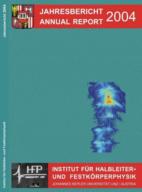
Cover Figures<br />
Background shows an array of ordered SiGe islands, fabricated by seeded MBE<br />
growth on a Si substrate prepatterned using e-beam lithography. (Figure periodically<br />
repeated)<br />
Inset at bottom right shows the x-ray diffraction pattern around the (224) reflection of a<br />
similar structure: here, a multilayer of ordered SiGe islands grown on a prepatterned<br />
Si substrate forms a 3D-island-quasicrystal, giving rise to a large number of<br />
stallite peaks in reciprocal space.
INSTITUT FÜR HALBLEITER- UND<br />
FESTKÖRPERPHYSIK<br />
JOHANNES KEPLER UNIVERSITÄT LINZ<br />
ANNUAL REPORT<br />
<strong>2004</strong><br />
PART A: Abteilung <strong>für</strong> <strong>Halbleiter</strong>physik<br />
Semiconductor Physics Group<br />
PART B: Abteilung <strong>für</strong> Festkörperphysik<br />
Solid State Physics Group<br />
PART C: Christian Doppler Laboratory for<br />
Surface Science Methods<br />
PART D: Lehre, Seminare und Symposia<br />
Teaching, Seminars, and Symposia<br />
A-4040 Linz, Altenbergerstrasse 69<br />
Tel.: +43-(0)732-2468-9600<br />
Fax: +43-(0)732-2468-8650<br />
e-mail: halbleiterphysik@jku.at<br />
internet: http://www.hlphys.jku.at
<strong>Institut</strong> <strong>für</strong> <strong>Halbleiter</strong>- und Festkörperphysik<br />
<strong>Institut</strong>e for Semiconductor and Solid State Physics<br />
Leiter / Head<br />
O.Univ.Prof. Dr. Günther BAUER<br />
e-mail guenther.bauer@jku.at<br />
Tel. +43-(0)732-2468-9600<br />
Fax +43-(0)732-2468-8650<br />
Abteilung <strong>für</strong> <strong>Halbleiter</strong>physik Abteilung <strong>für</strong> Festkörperphysik<br />
Semiconductor Physics Group Solid State Physics Group<br />
Leiter / Head: Leiter / Head:<br />
O.Univ.Prof. Dr. Günther BAUER Univ.Prof. Dr. Wolfgang JANTSCH<br />
e-mail: guenther.bauer@jku.at e-mail wolfgang.jantsch@jku.at<br />
Tel. +43-(0)732-2468-9601 Tel. +43-(0)732-2468-9641<br />
Secretary: Secretary:<br />
e-mail: halbleiter@jku.at e-mail evelyn.rund@jku.at<br />
Tel. +43-(0)732-2468-9600 Tel. +43-(0)732-2468-9639<br />
Fax +43-(0)732-2468-8650 Fax +43-(0)732-2468-9696<br />
Redaktion / edited by: G. Brunthaler, L. Palmetshofer, S. Lechner, E. Rund, A. Stangl
<strong>Annual</strong> <strong>Report</strong> <strong>2004</strong> v<br />
Preface<br />
Following the scheme of previous annual reports, we describe in this report the academic, research<br />
and teaching activities of the <strong>Institut</strong> <strong>für</strong> <strong>Halbleiter</strong>- und Festkörperphysik in the year<br />
<strong>2004</strong>. This report is organized in four parts, one for each of the two subdivisions of the <strong>Institut</strong>e,<br />
the Abteilung <strong>Halbleiter</strong>physik (headed by G. Bauer) and the Abteilung Festkörperphysik<br />
(headed by W. Jantsch). The third part presents achievements of the Christian Doppler Laboratory<br />
headed by K. Hingerl, the fourth part gives an overview over the teaching activities of<br />
the institute.<br />
Graduations, scientific achievements<br />
In <strong>2004</strong>, four people graduated from the institute as “Diplom-Ingenieur” and one PhD finished<br />
his studies successfully. They made important contributions to the scientific output of<br />
the institute. Again most of the papers of <strong>2004</strong> were published in Applied Physics Letters<br />
(12), there were 6 PRB’s and 1 PRL published under co-authorship of institute members.<br />
Among the highlights, there is the work on “ Two-flux composite fermion series of the fractional<br />
quantum Hall states in strained Si” by Lai et al. , which was done in collaboration with<br />
D.C. Tsui’s group at Princeton University. J. Stangl et al. published a review paper on “Structural<br />
characterization of semiconductor nanostructures” in Reviews of Modern Physics and<br />
on the cover page of the July <strong>2004</strong> issue of this journal appeared an AFM image of twodimensionally<br />
ordered Ge islands grown on patterned Si substrates by Zhenyang Zhong. In<br />
this year, the first vertically emitting IV-VI cw laser in the mid infrared was obtained in collaboration<br />
with the University of Bayreuth (Appl.Phys. Lett. 84, 3268 (<strong>2004</strong>), by J. Fürst et<br />
al) and an effective g-factor of up to 18000 was observed and reported for EuSe epilayers<br />
(Appl.Phys.Lett. 85, 67 (<strong>2004</strong>), by R. Kirchschlager et al.). Altogether the members of the<br />
institute published 22 papers in APS and AIP journals.<br />
Conference organization:<br />
In February <strong>2004</strong>, Wolfgang Jantsch, Friedemar Kuchar (Monatuniversität Leoben) and myself<br />
organized the International Winterschool on New Developments in Solid State Physics:<br />
Low-Dimensional Systems in Mauterndorf with 253 participants from all over world. The<br />
programme followed the tradition of this school with invited papers presented by eminent<br />
speakers and poster contributions in the in the fields of spin-related phenomena, quantum Hall<br />
transport, magnetic semiconductors, quantum dot applications, quantum dot optics, quantum<br />
dot transport., photonic band gap structures and novel electronic devices. The chairpersons of<br />
the sessions were asked to provide thorough introductions into these fields and they did a<br />
marvellous job. As usual the conference organisation and the local organization put quite a<br />
burden on our secretaries and our students and their enthusiastic help was essential for the<br />
success of this meeting.<br />
Friedrich Schäffler took a lot of the burdens in organizing the 54 th annual meeting of the Austrian<br />
Physical Society chaired by P. Zeppenfeld, 28-30 September at the <strong>JKU</strong> and other institute<br />
members contributed as well.<br />
Awards and Prizes:<br />
Julian Stangl received the Förderungspreis of the Land Upper Austria for his work on “Determination<br />
of strains and chemical composition in self-organised semiconductor islands”<br />
and Rainer Lechner received an award of the Sparkasse Oberösterreich for his outstanding<br />
PhD thesis. Helmut Heinrich was decorated by the Federal Ministry of Economics and Labour
vi <strong>Annual</strong> <strong>Report</strong> <strong>2004</strong><br />
of the Republic of Austria with the Österreichisches Ehrenzeichen <strong>für</strong> Wissenschaft und<br />
Kunst 1. Klasse.<br />
NanoScience and Technology<br />
Under the leadership of Friedrich Schäffler, several institutes of the Technical/Natural-<br />
Science Faculty (TNF) of our University and the Upper Austrian Research (UAR) brought<br />
together a consortium of three companies and four research institutions which submitted a<br />
proposal “Nanstructured Surfaces and Interfaces” (NSI) in the first call for proposals of the<br />
Austrian Nano Initiative, incited by the Austrian Council for Research and Technology. This<br />
Upper Austrian project cluster was successful in receiving a funding of € 1.5 Mio in <strong>2004</strong>, for<br />
six interlinked research projects for a duration of two years with work commencing in early<br />
2005. The NSI is coordinated by Friedrich Schäffler and cochaired by O Höglinger from the<br />
UAR and strengthens considerably the Nanoscience and Technology Center Linz (NSTL).<br />
Spezialforschungsbereich “IRON”<br />
A special research programme (Spezialforschungsbereich SFB 025) entitled “Infrared Optical<br />
Nanostructures” was established in collaboration with groups from the Technical University<br />
of Vienna, the Universities of Vienna and Jena, and the Technical University of Munich. The<br />
final decision on its funding was made by the Fonds zur Förderung der wissenschaftlichen<br />
Forschung, Vienna in October <strong>2004</strong> with the starting date of March 1 st , 2005. The principal<br />
investigators of five of the eleven granted projects are from this <strong>Institut</strong>e in Linz.<br />
Apart from that, four new FWF projects (by W. Heiß, A. Bonanni, G. Springholz (2)) and two<br />
EU projects in which G. Bauer and K. Hingerl are partners, were granted.<br />
Structure and personnel<br />
By the end of the year, the <strong>Institut</strong>e had 36 coworkers in the <strong>Halbleiter</strong>physik, 31 in Festkörperphysik,<br />
and 10 in the CD lab, so altogether 79 persons were working in the semiconductor<br />
physics building of our University.<br />
Helmut Heinrich retired in <strong>2004</strong> and is professor emeritus since 30 September <strong>2004</strong>. He<br />
founded the Solid State Physics group in Linz in 1972 which he led until 2003. Many of the<br />
present activities were initiated originally by him, e.g., ion implantation, epitaxy of IV-VI<br />
compounds, infrared detectors and emitters, and also the International Winterschool in Mauterndorf,<br />
together with G. Bauer and F. Kuchar. Among his scientific achievements, the socalled<br />
Heinrich- Langer rule attracted a lot of attention and it is still used to predict electronic<br />
leveles of transition metal impurities in semiconductors and band-offsets in heterostructures.<br />
He was Dean of the “Technisch-Naturwissenschaftliche Fakultät” in 1976-1979. In this period<br />
he committed himself successfully, among others, for the establishment of the Biophysics institute<br />
at <strong>JKU</strong> and he established the large instrument facility, now called TSE, which comprises<br />
instruments like electron microscopes, He- liquefier, etc.Helmut Heinrich was also the<br />
main driving force for a new chair in semiconductor physics in 1989 and 1990. He was president<br />
of the Austrian Physical Socienty (1978-80), board member of the Austrian Science<br />
Fund (1985-1994), of the Elektronik-holding and the VA Tech (ÖIAG) and chairman of the<br />
senate of the Christian Doppler Society (1995-<strong>2004</strong>). .<br />
Throughout <strong>2004</strong> our Rector had negotiations with the first candidate on the short list for the<br />
successor of Helmut Heinrich as a professor for Nanoscience and Ttechnology. Unfortunately,<br />
it was not possible to appoint the new professor before the end of <strong>2004</strong>.
<strong>Annual</strong> <strong>Report</strong> 2003 vii<br />
Among the technical personnel, E. Heissl, K. Haselgrübler and S. Stadler left the <strong>Institut</strong>e. We<br />
thank them for everything they did for us. New members – some of the well known already -<br />
are A. Praus, A. Stangl and E. Wirtl who joined us in <strong>2004</strong>.<br />
Altogether <strong>2004</strong> was an eventful year. Here I would like to thank all institute members, students<br />
and co-workers for their work and enthusiasm, not only in their own projects, but also in<br />
all other activities of the institute. Herewith I would like to thank also all our partners and colleagues<br />
abroad for their help and collaboration and to our sponsors:<br />
◦ Johannes Kepler Universität,<br />
◦ Austrian Federal Ministry of Science, Education and Culture,<br />
◦ Austrian Federal Ministry of Infrastructure,<br />
◦ Austrian Science Fund (FWF),<br />
◦ Gesellschaft <strong>für</strong> Mikro- und Nanoelektronik (GMe),<br />
◦ Fonds zur Förderung der Gewerblichen Wirtschaft (FFF)<br />
◦ Oberösterreichische Landesregierung,<br />
◦ Österreichischer Akademischer Austauschdienst,<br />
◦ and the Funds of the European Union.<br />
Finally, I would like to thank Gerhard Brunthaler and Leopold Palmetshofer who accepted the<br />
tedious task of being editors for this report.<br />
Guenther Bauer Linz, September 2005
Table of contents<br />
Preface....................................................................................................................... v<br />
PART A: Semiconductor Physics Group ............................................ 1<br />
Personnel .................................................................................................................. 2<br />
Scientific staff..................................................................................................................2<br />
Technical and support staff............................................................................................3<br />
Visiting researchers ........................................................................................................4<br />
Research visits of institute members ............................................................................4<br />
Dozent assigned to the institute.....................................................................................4<br />
Research Overview................................................................................................... 5<br />
Research Initiatives .................................................................................................. 7<br />
SFB025-IRON (Infrared Optical Nanostructures) ..........................................................7<br />
Project Cluster Nanostructured Surfaces and Interfaces (NSI)....................................8<br />
Research <strong>Report</strong>s ................................................................................................... 11<br />
High mobility Si/SiGe heterostructures for Spintronics applications........................12<br />
Fabrication of long-wavelength vertical-cavity surface-emitting lasers....................14<br />
Resonator fabrication for tunable Si/Ge quantum cascade detectors.......................16<br />
Lateral quantum dots in high-mobility heterostructures............................................18<br />
Surface evolution of self-assembled PbSe quantum dots .........................................20<br />
Self-organization of ripples and islands with SiGe-MBE............................................22<br />
Transmission electron microscopy (TEM) of nanostructures....................................24<br />
X-Ray study of epitaxially grown GaP nanowires .......................................................26<br />
X-Ray diffraction from a SiGe island quasicrystal ......................................................28<br />
X-Ray investigation of thick epitaxial GaAs/InGaAs layers on Ge.............................30<br />
Metallic state in two-dimensional Si-MOS structures .................................................32<br />
Electronic structure of self assembled pyramidal PbSe quantum dots ....................34<br />
Magnetic properties of self organized EuSe quantum dots .......................................36<br />
Diploma and Doctoral Theses ............................................................................... 39<br />
Diploma theses finished in <strong>2004</strong> ..................................................................................39<br />
Current diploma theses ................................................................................................39<br />
Doctoral thesis finished in <strong>2004</strong>...................................................................................39<br />
Current doctoral theses ................................................................................................39<br />
Publications ............................................................................................................ 41<br />
published <strong>2004</strong> ..............................................................................................................41<br />
submitted <strong>2004</strong> / in print ...............................................................................................44<br />
News Coverage..............................................................................................................46<br />
Talks and Presentations......................................................................................... 47<br />
Invited Talks ..................................................................................................................47<br />
Kolloquia and Seminar Talks........................................................................................47<br />
Conference Presentations (Talks and Posters)...........................................................48<br />
Funded Research Projects..................................................................................... 52<br />
Extramural Activities .............................................................................................. 55<br />
Gesellschaft <strong>für</strong> Mikroelektronik (GMe) .......................................................................55<br />
Fonds zur Förderung der wissenschaftlichen Forschung (FWF) ..............................55<br />
Industrial Collaborations........................................................................................ 56<br />
Organizational, Training, Awards.......................................................................... 56
<strong>Annual</strong> <strong>Report</strong> 2003 ix<br />
PART B: Solid State Physics Group ................................................. 57<br />
Personnel.................................................................................................................59<br />
Scientific staff................................................................................................................59<br />
Visiting researchers ...................................................................................................... 61<br />
Research visits of institute members .......................................................................... 62<br />
Research ..................................................................................................................63<br />
Research <strong>Report</strong>s....................................................................................................65<br />
Spin relaxation in zero dimensional SiGe islands ...................................................... 66<br />
Carrier-induced ferromagnetism in (Ga,Fe)N .............................................................. 68<br />
In situ characterization of MOCVD growth by x-ray diffraction ................................. 70<br />
Mid-infrared IV-VI vertical-emitting lasers ................................................................... 72<br />
Optoelectronic devices based on colloidal HgTe nanocrystals................................. 74<br />
Geometry dependent nucleation mechanism for SiGe islands.................................. 76<br />
Carrier mobility of Hot Wall epitaxially grown fullerene based transistors............... 78<br />
Diploma and Doctoral Theses................................................................................81<br />
Current diploma theses ................................................................................................ 81<br />
Current doctoral theses................................................................................................ 81<br />
Publications.............................................................................................................83<br />
published 2002 .............................................................................................................. 83<br />
submitted 2002 / in print ............................................................................................... 86<br />
Talks and Presentations .........................................................................................89<br />
Invited Talks ..................................................................................................................89<br />
Conference Presentations (Talks and Posters) .......................................................... 89<br />
Funded Research Projects .....................................................................................96<br />
Extramural Activities...............................................................................................97<br />
Industrial Collaborations ........................................................................................98<br />
PART C: CD Lab for Surface Science Methods................................ 99<br />
Personnel...............................................................................................................101<br />
Research <strong>Report</strong>s..................................................................................................102<br />
SOI material for 2D Photonic Crystal Applications................................................... 103<br />
Designing and Simulating disordered Photonic Crystals ........................................ 105<br />
Publications...........................................................................................................107<br />
Talks and Presentations .......................................................................................108<br />
Conference Presentations .......................................................................................... 108<br />
Talks at universities.................................................................................................... 108<br />
Visiting Researchers.............................................................................................108<br />
Research Projects .................................................................................................109<br />
PART D: Teaching, Seminars, and Symposia ................................ 111<br />
Winter Semester 2001/2002 ..................................................................................112<br />
Summer Semester 2002........................................................................................114<br />
Winter Semester 2003/<strong>2004</strong> ..................................................................................117<br />
Semiconductor Physics Seminar Talks ..............................................................119
x <strong>Annual</strong> <strong>Report</strong> <strong>2004</strong>
Part A<br />
Abteilung <strong>Halbleiter</strong>physik<br />
–<br />
Semiconductor Physics Group
2 Personnel Part A: Semiconductor Physics Group<br />
Personnel<br />
The scientific-personnel structure of the semiconductor physics group consists of:<br />
◦ 2 permanent professor positions (granted by ministry of science),<br />
◦ 4 permanent scientific member positions (granted by ministry of science),<br />
◦ 2 full non-permanent scientific member positions (PhDs granted by ministry of science),<br />
◦ 16 non-permanent scientific member positions (granted by FWF, EC, ÖAD),<br />
Thus, for each permanent staff member an average of about 3 non-permanent research positions<br />
were acquired through granted research projects.<br />
Scientific staff<br />
Researchers funded by ministry of science<br />
name degree position<br />
Günther Bauer Dr. O. Univ.-Prof.<br />
Friedrich Schäffler Dr. Univ.-Prof.<br />
Gerhard Brunthaler Doz. Dr. Ao.-Prof.<br />
Gunther Springholz Doz. Dr. Ao.-Prof.<br />
Thomas Fromherz Dr. Univ.-Ass.<br />
Julian Stangl Dr. Univ.-Ass.<br />
Graduate (PhD) students<br />
name degree funding graduated<br />
Laurel Abtin M.Sc. FWF<br />
Thomas Berer Dipl.Ing. Univ. Linz<br />
Daniel Gruber Dipl.Ing. Univ. Linz<br />
Rainer T. Lechner Mag. FWF April <strong>2004</strong><br />
Herbert Lichtenberger Dipl.Ing. FWF<br />
Dmytro Lugovyy M.Sc. FWF<br />
Rajivsingh Mundboth M.Sc. FWF<br />
Jiri Novak M.Sc. EC (SiGeNET, SHINE)<br />
Dietmar Pachinger Dipl.Ing. FWF<br />
Georg Pillwein Dipl.Ing. FWF<br />
Patrick Rauter Dipl.Ing. EC (SHINE)<br />
Aaliya Rehman M.Sc. ÖAD<br />
Wolfgang Schwinger Dipl.Ing. FFF<br />
Mathias Simma Dipl.Ing. FWF<br />
Eugen Wintersberger Dipl.Ing. EC (SHINE), FWF
Part A: Semiconductor Physics Group: Personnel 3<br />
Post docs<br />
name degree funding<br />
Rainer Lechner Dr. FWF<br />
Mojmir Meduna Dr. EC (SHINE)<br />
Thomas Schwarzl Dr. FWF<br />
Diploma students<br />
name<br />
Martyna Grydlik<br />
Thomas Hörmann<br />
graduated<br />
Stefan Janecek July <strong>2004</strong><br />
Benjamin Lindner November <strong>2004</strong><br />
Bernhard Mandl (in co-operation with University of Lund, Sweden)<br />
Mathias Simma May <strong>2004</strong><br />
Eugen Wintersberger February <strong>2004</strong><br />
Technical and support staff<br />
name position<br />
Friedrich Binder mechanic<br />
Stephan Bräuer clean room technician<br />
Alma Halilovic laboratory technician<br />
Ursula Kainz a laboratory technician<br />
Antonia Praus b laboratory technician<br />
Susanne Lechner, Mag. administration<br />
Sabine Stadler c administration<br />
Alexandra Stangl d administration<br />
Ernst Vorhauer, Ing. (HTL-Elektronik) electronics engineer<br />
a till 7. Nov. <strong>2004</strong>, b since 8. Nov. <strong>2004</strong>, c Jan. – Nov. <strong>2004</strong>, d since Dec. <strong>2004</strong>
4 Personnel Part A: Semiconductor Physics Group<br />
Visiting researchers<br />
name home institution duration<br />
Vaclav Holy, Prof. Charles Univ. Prag 2 months<br />
Sigurd Wagner, Prof. Princeton Univ. 1 month<br />
Research visits of institute members<br />
name visit to<br />
G. Bauer DESY Hamburg, ESRF Grenoble, Masaryk Univ. Brno<br />
R. Lechner DESY Hamburg, ESRF Grenoble<br />
J. Stangl DESY Hamburg, ESRF Grenoble<br />
E. Wintersberger DESY Hamburg, ESRF Grenoble, Masaryk Univ. Brno<br />
A. Rehman DESY Hamburg, ESRF Grenoble<br />
Dozent assigned to the institute<br />
name permanent address<br />
Ernest Fantner, Doz. Dr. IMS Wien
Part A: Semiconductor Physics Group: Research Overview 5<br />
Research Overview<br />
Nanostructures<br />
The central research focus of the institute is on semiconductor hetero- and nanostructures,<br />
thus forming a strong building block of the “Nanoscience and Technology” research activities<br />
of the Johannes Kepler University Linz. The research work at our institute encompasses all<br />
aspects of semiconductor nanostructures, ranging from nanofabrication, to fundamental investigations<br />
and modeling of physical properties, up to the realization of novel nanostructure devices.<br />
Nanostructures are fabricated using advanced lithography and processing techniques<br />
such as electron beam lithography as well as by self-assembly based on molecular beam epitaxy.<br />
For these purposes, a class 100 clean room facility with all the necessary processing<br />
equipment is run at the institute. The objective of nanofabrication is to produce defect free<br />
structures in the sub 50 nm range with good control of shapes and compositions with sharp<br />
heterointerfaces and excellent optical and electronic properties. A particular emphasis is on<br />
the development of site-control techniques for positioning of self-assembled nanostructures.<br />
Physical Properties<br />
The fundamental structural, electronic, optical and magnetic properties of nanostructures are<br />
studied using a wide range of techniques. These range from advanced x-ray scattering techniques<br />
using synchrotron radiation, high-resolution electron microscopy, scanning force and<br />
scanning tunneling microscopy, optical spectroscopy as well as low temperature magnetotransport<br />
measurements. The focus of research is to correlate the electronic properties of<br />
nanostructures with the fabrication processes and structural properties, taking advantage of<br />
the complementarity of information gained by the available wide range of techniques and<br />
modeling tools. A strong emphasis is on infrared spectroscopy of the interband and instersubband<br />
electronic transitions in SiGe and narrow band gap semiconductors heterostructures, as<br />
well as on ballistic and quantum transport studies of SiGe and III-V hetero- and nanostructures<br />
in the milli Kelvin temperature regime. In addition, the magnetic properties of magnetic<br />
semiconductor hetero- and nanostructures are investigated and novel tools for nanostructure<br />
investigations based on synchrotron light sources are developed.<br />
Devices<br />
Several research activities are devoted to the fabrication of semiconductor hetero- and nanostructure<br />
devices, ranging from mid-infrared intersubband and interband detectors, quantum<br />
cascade structures, mid-infrared vertical cavity surface emitting lasers, resonant cavity detectors,<br />
to transport devices such as quantum dot and single electron transistors. In addition,<br />
novel spintronic devices that take advantage of the spin degree of freedom in order to produce<br />
new functionalities are developed.<br />
Materials<br />
From the materials side, a strong focus is on Si/SiGe/SiGeC based hetero- and nanostructures<br />
for which a large molecular beam epitaxy system is operated in the clean room of the institute.<br />
In addition, there is extensive work on narrow gap IV-VI compound semiconductors, which<br />
includes PbSe as well as PbTe based materials as well as the magnetic europium chalcogenide<br />
semiconductors. For these materials another two molecular beam epitaxy systems are available<br />
at the institute. The fabricated structures are supplied also to external research groups<br />
outside of the institute in the framework of long term international collaborations. On the<br />
other hand, also materials and structures including SiGe as well as GaAs/GaAlAs based structures<br />
are supplied from outside groups for further processing and analysis with techniques developed<br />
at our institute.
6 Research Overview Part A: Semiconductor Physics Group<br />
The research activities are embedded in several large research initiatives and project clusters<br />
such as the IRON special research program, the NIS Nanostructured Surface and Interface<br />
project cluster, as well as the SANDiE European network of excellence and several other EU<br />
funded research projects, more details are given in the other parts of the annual report.<br />
Experimental facilities<br />
Growth of low dimensional semiconductor heterostructures:<br />
◦ Riber SIVA SiGeC molecular beam epitaxy system<br />
◦ Riber 1000 and Riber 32 molecular beam epitaxy system for IV-VI semiconductors<br />
◦ Varian Gen II molecular beam epitaxy system for IV-VI semiconductors<br />
Processing and fabrication of nanostructures:<br />
◦ 200 m 2 clean room with areas of class 100 – 10000<br />
◦ optical lithography (mask aligner) for front and bottom side<br />
◦ holographic lithography<br />
◦ electron beam lithography<br />
◦ reactive ion etching<br />
◦ SiO2, Si3N4 plasma deposition<br />
◦ electron beam evaporation system for metallization<br />
◦ wafer bonder<br />
◦ diffusion ovens<br />
Surface analysis, structural, optical, electrical, and magnetic investigations:<br />
◦ UHV-scanning tunneling microscopes<br />
◦ Atomic force microscopes<br />
◦ Scanning electron microscope<br />
◦ Nomarski microscopes<br />
◦ Three high-resolution X-ray diffractometers, one with multilayer x-ray mirror<br />
◦ Rotating anode X-ray system with four-circle diffractometer<br />
◦ Two Fourier-transform infrared spectrometers including cryostats and magnet systems<br />
◦ Photoluminescence setup (Ar ion laser, Nd:Yag laser, grating spectrometer)<br />
◦ CO2 and CO lasers for spectroscopy<br />
◦ Several high-field and low-temperature superconducting magnet systems with He3 cryostat<br />
(8 and 16 T, down to 0.3 K)<br />
◦ SQUID-susceptometer for magnetization studies<br />
◦ Parmeter analyzer and LCR bridge<br />
◦ Wafer Probe
Part A: Semiconductor Physics Group: Research Initiatives 7<br />
Research Initiatives<br />
Special Research Programme SFB025-IRON: „Infrared Optical<br />
Nanostructures“<br />
Günther Bauer<br />
In <strong>2004</strong> one of the main activities was the preparation of a proposal for a special research programme<br />
together with groups from the Technical University of Vienna, the theory groups<br />
from the University of Vienna, the Technical University of Munich and the University of Jena.<br />
These efforts were successful and after getting approval from an international review panel<br />
with scientists from the United Kingdom, Sweden, Switzerland and the USA in September<br />
<strong>2004</strong>, in October <strong>2004</strong> the FWF finally provided funds for the first four years, starting with<br />
March 1 st 2005. If successful, the SFB 025 has the chance of getting prolonged for additional<br />
six years, thus its entire duration can last for 10 years. For the scientists involved ( F. Schäffler,<br />
Wolfgang Heiß, Gunther Springholz, Thomas Fromherz, Julian Stangl, and Günther<br />
Bauer) from the <strong>Institut</strong> <strong>für</strong> <strong>Halbleiter</strong>-and Festkörperphysik in Linz, in total 10 PhD and postdoc<br />
positions were granted. This SFB, the third one granted by the FWF in the field of physics<br />
in Austria, will undoubtedly have a strong impact on the future research activities of the<br />
institute in Linz.<br />
The objective of this "Spezialforschungsbereich IRON" is to employ semiconductor nanostructures<br />
in order to overcome the shortage of efficiently functioning optoelectronic semiconductor<br />
devices in the 2 to 20 µm wavelength range. In order to achieve this goal we plan to<br />
make significant advances in the understanding and development of novel nanostructuers for<br />
future midinfrared devices.<br />
Its mission is defined by the following scientific goals:<br />
1) to obtain new physical insights in carrier and spin dynamics, infrared response, energy<br />
level schemes and many body effects in quantum confined nanostructures<br />
2) to advance state of the art nanofabrication through self-assembled growth of quantum dots ,<br />
their ordering on prepatterned substrates as well as by epitaxial integration of chemically<br />
synthesized nanocrystals and by modelling growth dynamics<br />
3) to develop novel infrared quantum dots devices by exploiting and engineering the singular<br />
density of states, by tuning of the electronic coupling between quantum dots and by photon<br />
confinement using photonic band gap structures.<br />
Furthermore it will establish long term interdisciplinary partnerships between leading research<br />
institutions in Austria and Germany, and broadly train and educate young researchers in the<br />
fields of nanotechnology, infrared photonics, spin photonics, quantum physics and optoelectronics.<br />
More information: http://www.hlphys.uni-linz.ac.at/hl/IRON_SFB/IRON_SFB.html<br />
Funding: FWF, GME<br />
Corresponding Author: Guenther.Bauer@jku.at
8 Research Initiatives Part A: Semiconductor Physics Group<br />
Project Cluster Nanostructured Surfaces and Interfaces (NSI)<br />
F.Schäffler<br />
Three years ago the Austrian Council for Research and Technology Development proposed an<br />
Austrian Nano Initiative to strengthen the national activities in the<br />
field of NanoScience and Technology. In <strong>2004</strong> FFG and FWF, the<br />
two funding agencies administering the program, issued the First<br />
Call for Program Line I: Project Clusters in this emerging interdisciplinary<br />
field. The Johannes Kepler University (<strong>JKU</strong>) and Upper<br />
Austrian Research (UAR), the research institution of the province<br />
of Upper Austria, brought together a consortium of three companies<br />
and four research institutions, which participated in the First<br />
Call with their proposal Nanostructured Surfaces and Interfaces (NSI). Following the suggestions<br />
of an international refereeing board, five out of a total of eight consortia proposals submitted<br />
to the First Call were awarded funding for a two-year period each. The project cluster<br />
NSI, which consists of six interlinked research projects, receives funding of € 1.5 Mio. NSI is<br />
coordinated by F. Schäffler from the <strong>Institut</strong> for Semiconductor Physics; and co-chaired by O.<br />
Höglinger from UAR. Project work is scheduled to commence in early 2005.<br />
The purpose of NSI is, to link the expertise and infrastructure in the field of NanoScience<br />
and Technology, which was systematically developed since the early 1990s in Linz and Upper<br />
Austria, and to make them available to both the Austrian industry and to education inside and<br />
outside the university. NSI is expected to convert the as yet loosely linked NanoScience and<br />
Technology activities in Linz into a nationally and internationally competitive center of excellence.<br />
It is intended to develop NSI into a local node in the emerging Austrian NanoScience<br />
and Technology Network, located in Upper Austria, the leading industrial center of Austria. In<br />
terms of education, the research projects of NSI provide qualified research positions for the<br />
students of the first Austrian NanoScience and Technology course, which was launched in<br />
2002 at the Johannes Kepler University in Linz.<br />
NSI covers three of the four main competence areas of the NanoScience and Technology<br />
activities in Linz and Upper Austria, and makes them available to the concept of the Austrian<br />
Nano Initiative. These three competence fields are Biocompatible Nanostructures, Polymers<br />
and Nanocomposites, and Metal Surfaces and Interfaces. Semiconductor Nanostructures, the<br />
fourth core competence in Linz, is already more advanced regarding its national and international<br />
integration and will mainly be pursued in the recently installed, international Spezialforschungsbereich<br />
IR-ON. Links between NSI and IR-ON exist via participation of the <strong>Institut</strong>e<br />
for Semiconductor and Solid State Physics in several of the NSI projects. This way the<br />
expertise and infrastructure available in and around the cleanroom of the institute is made<br />
available in an interdisciplinary approach to the other core competence areas.<br />
In the following, the six projects of NSI are briefly outlined, ordered with respect to the<br />
three aforementioned competence areas. The structure of IR-ON is treated in a separate article<br />
in this annual report.<br />
1. Biocompatible Nanostructures<br />
1.1 Nanostructured und Biofunctionalized Surfaces (NABIOS). In this project methods and<br />
techniques from semiconductor technology and surface science are combined with molecular<br />
chemistry and single molecule spectroscopy. In a first step, gold surfaces are nanostructured<br />
by e-beam lithography at the <strong>Institut</strong>e for Semiconductor Physics. Simultaneously, the Insti-
Part A: Semiconductor Physics Group: Research Initiatives 9<br />
tute for Biophysics develops linker molecules that allow binding of a single bio-molecule on<br />
each of the nanopatterned Au islands. Finally, UAR provides single molecule detection using<br />
the fluorescence microscope ("nanoreader") they developed recently in the framework of the<br />
national GEN-AU project. NABIOS combines in an interdisciplinary way the technologies an<br />
expertise of groups in three differen fields of NanoScience and Technology.<br />
1.2 Nano-Biocompatible Polymerfoils (NBPF). In this project the surfaces of polymer foils<br />
are nanostructured by laserradiation in a way that allows the ordered arrangement of cell cultures<br />
for medical diagnosis and therapy. This approach provides a local modification of the<br />
polymer surface that avoids the disadvatages of conventional techniques, such as reduced mechanical<br />
stability or enhanced bio-degradation. The consortium comprises the institutes for<br />
Applied Physics and Biophysics (both <strong>JKU</strong>) for laser patterning and bio-compatibility, and<br />
the <strong>Institut</strong>e for Pharmacology and Toxicology (Univ. Vienna) for the automatic positioning<br />
of cell cultures.<br />
2. Polymers und Nanocomposites<br />
2.1 Nanometric Organic Actuators (NANORAC). This entirely new approach employs organic<br />
semiconductors to realize nano-electromechanical (NEM) functionality. As yet, dielectrics<br />
were utilized for such purposes, which are not easily integrated into electronic circuits. The<br />
new approach aims toward organic actuators that can be controlled by integrated organic electronic<br />
components. NANORAC combines the expertise of the Linz <strong>Institut</strong> for Organic Solarcells<br />
(LIOS) und der Group for the Physics of Soft Matter, both from <strong>JKU</strong>.<br />
2.2 Sol-Gel-enhanced Catalysts for the Fabrication of Carbon-Nanotubes (SolTube). Carbon-<br />
Nanotubes (CNT) are an intense research area for a large number of potential applications..<br />
SolTube introduces a Sol-Gel-Process for the deposition of a homogeneous dispersion of Nanopartikels<br />
on a surface. These then work as catalysts for the growth of a densely packed<br />
CNTs. In the long run, membranes consisting of dense arrays of CNTs are envisaged for nanofiltration<br />
purposes. SolTube is led by the company Profactor from Steyer near Linz, which<br />
provide the sol-gel process. Electrovac, a leading European manufacturer of CNTs provides<br />
the facilities for the growth of CNTs. This project is supported by the analytical tools and expertise<br />
in CVD growth of CNTs available in university institutes in Linz and at TU Vienna.<br />
3. Nanostructured Metal Surfaces and Interfaces<br />
3.1 Optical Properties of Metal Clusters on Crystalline Surfaces (MetClust). In this project<br />
the basic properties of nanometer-sized metal clusters on crystalline PET und quartz-<br />
Oberflächen are investigated with optical und magneto-optical methods. In particular, Reflectance<br />
Difference Spectroscopy (RDS) will be employed, a field in which pioneering contributions<br />
were made in Linz. The project is coordinated by the <strong>Institut</strong>e for Surface Science, with<br />
contributions from the <strong>Institut</strong>e for Solid State Physics, and the company Hueck Folien.<br />
3.2 In-Line-Characterization of Nanometer-Thick Metallayers on Polymerfoils (PolyMet).<br />
This project is closely related to MetClust, and aims toward an exploitations of the optical<br />
techniques developed in MetClust for industrial surveillance of foil production lines. For this<br />
purpose a prototype set-up will be developed for in-line control of nm-thick metal films on<br />
polymer foils. This project is a collaboration between Hueck Folien and the <strong>Institut</strong>e for Surface<br />
Physics.<br />
More Information: www.nanoscience.at<br />
Funding: Austrian Nano Initiative (FFG, FWF)<br />
Corresponding Author: Friedrich.Schaffler@jku.at
10 Research Initiatives Part A: Semiconductor Physics Group
Part A: Semiconductor Physics Group: Research <strong>Report</strong>s 11<br />
Technology and devices<br />
Research <strong>Report</strong>s<br />
◦ High mobility Si/SiGe heterostructures for Spintronics applications 12<br />
◦ Fabrication of long-wavelength vertical-cavity surface-emitting lasers 14<br />
◦ Resonator fabrication for Si/Ge quantum cascade detectors 16<br />
◦ Lateral quantum dots in high-mobility heterostructures 18<br />
Growth phenomena<br />
◦ Surface evolution of self-assembled PbSe quantum dots during overgrowth 20<br />
◦ Self-organization of ripples and islands with SiGe-MBE 22<br />
Structural, electronic, and optical characterization<br />
◦ Transmission electron microscopy (TEM) of nanostructures 24<br />
◦ X-Ray study of epitaxially grown GaP nanowires 26<br />
◦ X-Ray diffraction from a SiGe island quasicrystal 28<br />
◦ X-Ray investigation of epitaxial GaAs/InGaAs layers on Ge 30<br />
◦ Metallic state in two-dimensional Si-MOS structures 32<br />
◦ Electronic structure of self assembled pyramidal PbSe quantum dots 34<br />
◦ Magnetic properties of self organized EuSe quantum dots 36
12 Research <strong>Report</strong>s Part A: Semiconductor Physics Group<br />
High mobility Si/SiGe heterostructures for Spintronics applications<br />
D. Gruber, H. Malissa, D. Pachinger, F. Schäffler, W. Jantsch,<br />
A. M. Tyryshkin 1 and S. A. Lyon 1<br />
The Silicon Germanium (SiGe) material system is a promising candidate for solid-state spintronics<br />
applications due to its very long spin relaxation times and its compatibility to standard<br />
Si process technology. There are proposals for spin transitors in the SiGe material system<br />
which could be used for Quantum Computing. For this application very long spin coherence<br />
times and the ability to control and to read spin orientation is necessary. We work towards the<br />
demonstration of the ability to control the g-factor of electron spins in SiGe Quantum well<br />
structures by applying electrical fields, which can be used for selective spin manipulation.<br />
Our samples are grown in a Molecular Beam Epitaxy (MBE) system with electron beam<br />
evaporators for Si and Ge. The channels are n-type modulation-doped with Sb. High mobilities<br />
of up to µe = 250,000 cm 2 /Vs have been reached in pure Si channels without back gate.<br />
The spin lifetimes are extremely long as well: Spin-echo measurements give T1 = 2.3 µs and<br />
T2= 3 µs for a magnetic field perpendicular to the 2DEG plane [1]. The high quality of our<br />
samples was also shown in recent magneto-transport experiments, where the ν=1/3, 4/7 and<br />
4/9 composite fermion states in the fractional quantum Hall effect were seen for the first time<br />
in the SiGe material system [2].The samples are either pure Si wells or double quantum well<br />
(QW) structures with a pure Si well and one with 5% Ge, which are separated by a barrier<br />
with 15% Ge content. The second structure is designed in a way that by applying electrical<br />
fields relative to the quantum wells one can completely shift the electronic wave function<br />
from one well to the other as depicted in a self-consistent band structure simulation in Fig. 1.<br />
Hand in hand with the change in the surrounding material goes a change in g-factor of the<br />
electrons [3] and hence a change in resonance frequency in an Electron Spin Resonance<br />
(ESR) experiment. Spin manipulation via pulsed ESR techniques is then possible on the spins<br />
which have been shifted into resonance.<br />
Fig. 1: Self-consistent band structure calculation of the double quantum well structure (as<br />
shown above and right) with different applied backgate fields: A front gate was used to keep<br />
the carrier concentration at a constant density of ns=3x10 11 cm -2 . The calculated change in gfactor<br />
can be estimated as ∆g = 2.5x10 -4 , which is enough to separate the resonances and<br />
allow spin manipulation.<br />
The required electrical fields are created by applying voltages to a Schottky-type topgate<br />
and either a grown-in n-type backgate or an evaporated Al backgate on the backside of the<br />
sample. Fig. 2. shows how the carrier density and the mobility can be changed in a pure Si<br />
channel with Schottky topgate and evaporated Al backgate. Our next goal is the combination<br />
of front- and backgate and the double QW structure.
Part A: Semiconductor Physics Group: Research <strong>Report</strong>s 13<br />
Fig. 2: Carrier density and mobility of a sample with pure Si channel with a Pd Schottky gate<br />
on top and an evaporated Al backgate on the back side plotted as a function of the topgate<br />
voltage for different backgate voltages. Both mobility and carrier density can be influenced<br />
by shifting the wave function away from the interface (higher backgate voltages).<br />
In summary, we report about a SiGe double QW structure designed for tuning the electronic<br />
g-factor of electrons. Simulations show that it is possible to completely shift the electronic<br />
wave function between two wells with different Ge content and hence the g-factor<br />
which is a requirement for quantum computing in SiGe. The process for top- and backgate<br />
electrodes is established, and demonstrated on a single Si well sample. The next step will be<br />
the combination of double QW structure and front- and backgate.<br />
References<br />
1. A. M. Tyryshkin, S. A. Lyon, W. Jantsch, and F. Schäffler, PRL 94, 12802 (2005)<br />
2. K. Lai, W. Pan, D.C.Tsui, S. Lyon, et al., PRL 93, 156805 (<strong>2004</strong>)<br />
3. H. Malissa, W. Jantsch, M. Mühlberger, F. Schäffler, Z. Wilamowski, M. Draxler, and P. Bauer, APL 85,<br />
1739 (<strong>2004</strong>)<br />
Collaborations<br />
A. M. Tyryshkin 1 and S. A. Lyon 1 , Department of Electrical Engineering, Princeton University, Princeton, NJ<br />
08544 USA<br />
Funding<br />
FWF, GME<br />
Corresponding Author: daniel.gruber@jku.at
14 Research <strong>Report</strong>s Part A: Semiconductor Physics Group<br />
Fabrication of long-wavelength vertical-cavity surface-emitting lasers<br />
with cw emission at 6-8 microns<br />
G. Springholz, T. Schwarzl, M. Böberl, W. Heiss, J. Fürst 1 , and H. Pascher 1<br />
Narrow bandwidth coherent mid-infrared emitters of great importance for ultrahigh-sensitive<br />
gas analysis and atmospheric pollution monitoring because the strong absorption lines of all<br />
molecular gases are found in this spectral region. The IV-VI semiconductors are particularly<br />
very well suited for these devices due to their nearly symmetric conduction and valence bands<br />
and the very small non-raditative Auger recombination rates. Over the last few years, we have<br />
developed a novel class of MIR lasers based on ultra-high finesse epitaxial vertical cavity<br />
structures. The resulting IV-VI vertical cavity surface emitting lasers (VCSELs) offer several<br />
advantages such as very small beam divergence, single mode operation and the possibility of<br />
monolithic integration. In addition, they can be grown on readily available BaF2 substrates,<br />
which have a much higher thermal conductivity than high-cost IV-VI substrates.<br />
In the present work, we report the fabrication and operation of the first infrared VCSELs<br />
operating in cw mode at very long wavelengths up to 8 µm. The structures were grown by<br />
molecular beam epitaxy on (111) oriented BaF2 [1]. As PbSe emits at wavelengths longer<br />
than 6.5 µm only at cryogenic temperature, the lasers were designed for operation temperatures<br />
below 100 K. The microcavity structure is formed by two high-reflectivity epitaxial<br />
Bragg mirrors consisting of five λ/4 EuSe/Pb0.94Eu0.06Se layer pairs. Due to the high refractive<br />
index contrast a reflectivity of 99.5% is achieved already by a few layer pairs. The 2 λ cavity<br />
region of the VCSEL designed for 7.9 µm emission wavelength consists of a 2.2 µm<br />
Pb0.94Eu0.06Se buffer and a 1.1 µm PbSe active region.<br />
Figure 1 (a) shows the reflectivity spectrum of the VCSEL. At 300 K, the spectrum exhibits<br />
three narrow cavity resonances of m = 3 rd , 4 th and 5 th order. The line width of the central<br />
4 th order mode is only 0.10 meV, demonstrating a high finesse of 400. Owing to the decrease<br />
of the PbSe band gap, at low temperatures the higher energy cavity resonances are damped by<br />
interband absorption. Thus, at 60 K (see insert), the 4 th order cavity resonance is broadened to<br />
0.13 meV and disappears at even lower temperatures. The VCSELs were optically pumped<br />
using a 5.28 µm cw-CO laser and the total emitted power was measured using a calibrated<br />
detector using an InSb long pass filter. Figure 1 (b) shows the emitted laser line for cw as well<br />
as pulsed excitation. At 2 K, laser emission is found at the 4 th order resonance at 156.51 meV<br />
or λ = 7.92 µm, which represents the longest emission wavelength of all VCSELs reported to<br />
date. For cw operation, an extremely narrow line width of only 12µeV or 0.6 nm is observed.<br />
Reflectivity (%)<br />
100<br />
90<br />
80<br />
70<br />
60<br />
50<br />
40<br />
30<br />
20<br />
10<br />
0<br />
(a) 7.9 µm VCSEL<br />
0.1 meV<br />
FWHM<br />
300 K<br />
m=3<br />
m=4<br />
m=5<br />
Transmission (a.u.)<br />
60 K<br />
m = 4<br />
FWHM<br />
0.13 meV<br />
158.0 158.5<br />
120 140 160 180 200<br />
Energy (meV)<br />
220 240 260<br />
Normalized emission<br />
(b)<br />
excitation power<br />
400 mW<br />
cw<br />
FWHM 12 µeV<br />
(spectrometer<br />
resolution)<br />
7.9 µm VCSEL<br />
2 K<br />
pulsed<br />
FWHM 45 µeV<br />
156.40 156.44 156.48 156.52 156.56 156.60<br />
Energy (meV)<br />
Figure 1: (a) Reflectivity of a 7.9 µm cw-PbSe/EuSe VCSEL measured at 300 K. The insert<br />
shows the transmission around the central cavity mode at 60 K on an enlarged scale. (b)<br />
Emission spectra at 2 K in cw (dots) and pulsed mode (triangles) at 400 mW pump power.
Part A: Semiconductor Physics Group: Research <strong>Report</strong>s 15<br />
Emission Power (mW)<br />
10 0<br />
10 -2<br />
1x10 -4<br />
2 K<br />
7.9 µm VCSEL<br />
cw emission<br />
stimulated emission<br />
spontaneous emission<br />
Emitted Pulsed<br />
Peak Power (W)<br />
10<br />
1 10 100 1000<br />
-8<br />
10 -6<br />
5<br />
0<br />
0 100 200 300 400 500<br />
Pulsed Pump Power (W)<br />
CW Excitation Power (mW)<br />
25<br />
20<br />
15<br />
10<br />
pulsed emission<br />
(a)<br />
Emission Power (mW)<br />
0.4<br />
0.3<br />
0.2<br />
0.1<br />
7.9 µm VCSEL<br />
(b)<br />
0.3<br />
(mW)<br />
0.2<br />
Power<br />
cw excitation power<br />
0.1<br />
130 mW Emission<br />
0.0<br />
0 10 20 30 40 50<br />
Temperature (K)<br />
Figure 2: (a) Cw output power of the 7.9 µm VCSEL plotted as a function of pump power at 2<br />
K: (o) spontaneous emission, (●) laser emission. The 25 mW laser threshold is determined<br />
from the inflection point. Inset: pulsed laser output versus excitation power. (b) Cw output<br />
power of the same VCSEL at 130 mW pump power plotted versus operation temperature.<br />
This is 10 times smaller than width of the unpumped cavity resonance. It is also much narrower<br />
than that of the pulsed mode emission of 45 µeV (2.3 nm), whereas for cw-excitation it is<br />
exactly equal to the resolution of the spectrometer setup. Thus, the true cw line width is actually<br />
much smaller than 0.6 nm [1].<br />
Figure 2 (a) shows the logarithmic plot of the cw power emitted as a function of excitation<br />
power. For weak excitation, only spontaneous emission (o) is found but above threshold the<br />
emitted power rapidly increases (●). The external laser threshold is 25 mW, corresponding to<br />
an internal threshold of 25 W/cm 2 . At 1.2 W excitation, the emitted cw power is 4.8 mW,<br />
which is the highest value reported for any infrared cw VCSEL. The inset of Fig. 2 (a) shows<br />
the emitted pulse peak power as a function of pump power, in which case a peak output power<br />
as high as 23 W was achieved. Figure 2(b) shows the temperature dependent emission for a<br />
constant 130 mW pump power. As the temperature increases, the spontaneous PbSe emission<br />
shifts closer to the cavity resonance mode and thus emitted intensity is actually enhanced. At<br />
30 K, the spontaneous emission coincides with the cavity resonance, resulting in best laser<br />
performance. At higher temperatures, the spontaneous emission shifts above the cavity mode<br />
and thus, the laser emission is quenched. The laser wavelength can be tuned by +0.058<br />
meV/K or –2.1 nm/K as found for a 100 K VCSEL emitting at 6.7 µm. This is substantially<br />
larger as compared to that of III-V quantum cascade lasers. The emission can also be tuned by<br />
applying external magnetic fields [3]. The beam divergence is extremely narrow (below 1°).<br />
Because the operation temperatures up to now are only limited by the pump laser wavelength,<br />
already a few changes in the laser structure and the use of other pump sources are expected to<br />
lead to higher cw-laser operation temperatures.<br />
References<br />
1. J. Fürst, T. Schwarzl, M. Böberl, H. Pascher, G. Springholz W. Heiß “Continuous-wave emission from midinfrared<br />
IV–VI vertical-cavity surface-emitting lasers“ Appl. Phys. Lett. 84, 3268 (<strong>2004</strong>).<br />
2. T. Schwarzl, G. Springholz, M. Böberl, E. Kaufmann, J. Roither, W. Heiss, J. Fürst, and H. Pascher,<br />
“Emission properties of 6.7 µm continuous-wave PbSe-based vertical-cavity surface-emitting lasers<br />
operating up to 100 K“ Appl. Phys. Lett. 86, 031102 (2005).<br />
3. J. Fürst, H. Pascher, T. Schwarzl, G. Springholz, M. Böberl, G. Bauer, W. Heiss “Magnetic field tunable circularly<br />
polarized emission from mid-infrared vertical emitting lasers” Appl. Phys. Lett. 86, 021100 (2005).<br />
Collaborations<br />
1<br />
Experimentalphysik I, Universität Bayreuth, Universitätsstrasse 30, D-95447 Bayreuth, Germany.<br />
Funding: FWF and GME<br />
Corresponding Author: gunther.springholz@jku.at<br />
0.4<br />
0.0
16 Research <strong>Report</strong>s Part A: Semiconductor Physics Group<br />
Resonator Fabrication for Cavity Enhanced, Tunable Si/Ge Quantum<br />
Cascade Detectors<br />
M. Grydlik, P. Rauter, T. Fromherz, G. Bauer, L. Diehl 1 , C. Falub 1 , G. Dehlinger 1 , H. Sigg 1 ,<br />
D. Grützmacher 1 , G. Isella 2<br />
Infrared detection employing optical transitions in quantum wells has attracted a lot of research<br />
interest in the past several years. Due to the design freedom a variety of detector figures<br />
like for example the spectral region of sensitivity, the response time, the detector noise<br />
etc. can be adjusted over a large parameter range and optimized detector performance can be<br />
achieved for several areas of applications. In a recent work on SiGe QWIPs, we have demonstrated<br />
that in addition a large wavelength tunability can be achieved by employing the injector<br />
concept originally developed for quantum cascade electro-luminescence and laser structures<br />
[1]. The detectivity of these tunable SiGe QWIPs at 77K is approximately 1.5 x 10 9<br />
cmHz 0.5 /W, typically 1-2 orders of magnitude smaller than the detectivity of group III-V<br />
based devices. One concept to increase the detectivity of SiGe QWIPs in a narrow detection<br />
bandwidth consists of integrating the QWIP into a vertical resonator. Since for QWIPs based<br />
on SiGe cascade structures, an extremely large tuning range from for example 200 meV to<br />
400 meV was demonstrated [1], the integration of this novel detectors into a properly designed<br />
vertical cavity will allow resonator enhanced detection for 2 narrow bands at wavelengths<br />
λ �and 2λ that can be addressed by the externally applied voltage.<br />
For integrating a tunable QWIP into a vertical cavity resonator, nominally the same QW<br />
sequence as described in Ref. [1] have been grown on a SOI substrate by low temperature (T=<br />
300°C) solid source MBE and processed into detectors. A similar tunability as reported previously<br />
[1] for detectors grown on Si substrate was achieved with these SOI based structures.<br />
For fabricating vertical cavity resonators, openings aligned to the detector mesas have to be<br />
etched from the backside of the sample trough the substrate. The buried oxide layer of the SOI<br />
substrate is used as an etch-stop. After removing the remaining SiO2 layer by an HF etch, a<br />
free standing film consisting of the detector QW sequences results. On the top and bottom<br />
side of this detector film, broadband, high-reflectivity metal or bragg – mirrors will be deposited<br />
that finally form the resonator.<br />
From the previous paragraph it is clear, that the choice of a proper etchant is crucial for<br />
successful resonator fabrication. In our work, TMAH (Tetramethylammonium Hydroxide) at<br />
90 °C was used as etchant for the following reasons: a) TMAH has reasonably large etchrate<br />
(30 µm/h) for the Si (001) lattice plane that allows to etch free the buried oxide layer of a<br />
thinned SOI substrate (200 µm) in approximately 7 h. b) In addition, the TMAH etch rate for<br />
Si (111) lattice planes is approximately an order of magnitude smaller than in (001) direction.<br />
Therefore, TMAH etch grooves are bound by (111) planes and negligible underetching of the<br />
etchmask occurs. c) The etchrate of TMAH for thermally grown oxide is virtually vanishing.<br />
Therefore the etching process is effectively stopped by the 200 nm thick buried oxide of the<br />
SOI substrate. Even after a 2 h long over-etching the exposed SiO2 layer showed no indication<br />
of an etch attack and remained optically flat. d) TMAH is compatible with the standard Si<br />
technology as it is contained in most of the photoresist developers.<br />
For the long etch times required to etch from the wafer backside to the buried SiO2, an etch<br />
mask with high resistance against TMAH is required. In standard Si MEM technology, a<br />
structured Si3N4 layer deposited by LPCVD at approximately 900°C is commonly used as<br />
mask for long TMAH etches. However, due to the high deposition temperature necessary for<br />
the LPCVD process, this mask material can not be used for samples with QWIP structures<br />
grown on the wafer frontside. On the other hand, a 300 nm thick Si3N4 deposited at lower<br />
temperatures (250 °C) in a plasma enhanced CVD (PECVD) process was destroyed by the
Part A: Semiconductor Physics Group: Research <strong>Report</strong>s 17<br />
TMAH etch after approximately 100 nm etch depth. Increasing the thickness of the Si3N4 to<br />
400 nm and 500 nm did not improve the results most probably due to increased number of<br />
strain induced cracks in the thicker the Si3N4 layers.<br />
The best results were obtained by a mask consisting of a double layer of Si3N4 (200 nm)<br />
and the spin-on polymer BCB (Bencocyclobutene, Dow Chemicals brand name: “Cyclotene”<br />
[2]) with a thickness of 6-8 µm. BCB can be structured by reactive ion etching in a mixed O2<br />
and CF4 plasma. The Si3N4 layer acts as an adhesion promoter for the BCB film. With this<br />
mask and a 10 h long TMAH etch, free standing Si membranes could be produced on a testwafer<br />
consisting of a Si layer grown on an SOI substrate instead of the Si/Ge QWIP structure.<br />
Electron and optical microscope pictures of the membrane are shown in Figs. 1 a-d. In the optical<br />
microscope (Figs. 1a, b) no surface roughness of the membrane and the (111) sidewalls<br />
are visible. The sample shown in Figs 1 a,b was illuminated from the backside resulting in a<br />
bright appearance of the Si membranes, indicating that the membranes are transparent in the<br />
visible spectral region due to their small thicknesses. Also the electron microscope pictures<br />
(Figs. 1 c,d) do not show significant surface roughness of the membranes and the sidewalls.<br />
The etchmask shown in Fig. 1 d is evidently not attacked by the TMAH etch and only a small<br />
underetching due to the non-vanishing etchrate in (111) direction is shown. Infrared transmission<br />
through a Si membrane was measured with an infrared microscope. The transmission<br />
spectrum plotted in Fig.1e shows strong Fabry-Perot oscillations with a periodicity corresponding<br />
to a membrane thickness of 1.42 µm.In future work, the linewidth and of these oscillation<br />
will be decreased by increasing the cavity Q-factor with high-reflectivity broadband<br />
mirrors deposited on the membrane surfaces.<br />
Fig.1: Results obtained by visible (a,b), electron (c,d) and infrared microscope (e) experiments revealing an<br />
optically flat Si membrane with thickness of 1.42 µm fabricated by the process described in the text.<br />
References<br />
1. P. Rauter, T.Fromherz, G. Bauer,L. Diehl, G. Dehlinger, H. Sigg, D. Grützmacher, H. Schneider, “Voltage<br />
tuneable, two-band MIR detection based on Si/SiGe quantum cascade injector structures“, Appl. Phys. Lett.<br />
83, 3879-3881 (2003).<br />
2. http://www.dow.com/cyclotene/<br />
Collaborations<br />
1<br />
Laboratory for Micro- and Nanotechnology, Paul-Scherrer <strong>Institut</strong>e, CH-5232 Villigen PSI, Switzerland;<br />
2<br />
Politecnico di Milano, 22110 Como, Italy<br />
Funding: BMVIT (Proj. Nr. GZ 604000/14-III/I5/2003), EC project SHINE (IST-2001-38035), GME.<br />
Corresponding Author: Thomas.Fromherz@jku.at
18 Research <strong>Report</strong>s Part A: Semiconductor Physics Group<br />
Lateral Quantum Dots in High-Mobility Heterostructures<br />
G. Pillwein, T. Berer, G. Brunthaler, F. Schäffler, and G. Strasser 1<br />
Lateral quantum dots are discussed as a promising option to realize the quantum entanglement<br />
necessary for quantum computation [1]. We have fabricated single quantum dot devices in the<br />
two-dimensional electron gas (2DEG) of both GaAs/AlGaAs and Si/SiGe heterojunctions.<br />
These devices are the basic building blocks of more complex structures (e.g. [2]), which we<br />
plan to investigate in the near future.<br />
The technology developed for the GaAs structures has been adapted to Si/SiGe based lateral<br />
quantum dots. Recently, several lateral quantum dots in silicon/silicon-germanium heterostructures<br />
have been reported e.g. [3]. However, none of these were achieved by the classical<br />
split-gate technique that is necessary for the coupling of quantum dots and for high integration.<br />
Both the GaAs/AlGaAs and Si/SiGe high mobility modulation doped heterostructures were<br />
grown by MBE, in the cleanrooms of TU Vienna and <strong>JKU</strong> Linz respectively. The 2DEG in<br />
these samples is typically situated around 80 nm below the surface.<br />
The electrical properties of the 2DEG were determined by quantum Hall effect and SdH<br />
measurements. The GaAs samples had a maximum mobility of 2x10 6 cm 2 /Vs at a carrier density<br />
of typically 2x10 11 cm -2 , the SiGe samples showed an electron mobility of 150000 cm²/Vs<br />
at an electron density of 3.2 x 10 11 cm -2<br />
Further processing of the samples was done in the cleanroom in Linz. Ohmic contacts, mesas<br />
and connection structures for the gates were structured by optical lithography. The split<br />
gate structures, which define the actual quantum dot, were written by e-beam lithography and<br />
defined by liftoff of Cr/Au (Pd) for GaAs (SiGe). Typical structures are shown in Fig. 1,<br />
where the top center gate electrode acts as a plunger gate.<br />
Fig.1: Scanning electron micrographs of a) the Cr/Au top gates on a GaAs/AlGaAs sample<br />
and b) the Pd split gates on a Si/SiGe sample. The pitch between the upper gates is 185nm<br />
When a negative voltage is applied to the gates the 2DEG beneath is depleted and the dot<br />
is defined in the central area. By varying the plunger gate voltage, the energy levels inside the<br />
dot can be moved into and out of resonance with the Fermi level in the leads. The conductance<br />
will increase, when the energies are aligned and decrease in between, forming the socalled<br />
Coulomb oscillations. If a large DC bias is applied at the source drain contacts the<br />
blockade can be overcome and excited energy states of the quantum dot can be probed.<br />
By measuring the conductance versus both the plunger gate voltage VG and the source<br />
drain voltage VSD, we obtain the so-called quantum dot spectrum. It gives access to a lot of<br />
information about the quantum dot. Such a measurement in the SiGe structure is shown in<br />
figure 2a below.
Part A: Semiconductor Physics Group: Research <strong>Report</strong>s 19<br />
Fig.2: Differential conductance of the a) SiGe and b) GaAs quantum dot as a function of gate<br />
voltage and applied dc source-drain voltage c) reproducible conductance fluctuations.<br />
From the size and shape of the rhombic regions (indicated by lines in Fig 2b) we can obtain<br />
electrical properties such as capacitances of the gates and leads with respect to the dot. By<br />
analyzing the measured Coulomb diamonds for the SiGe device (Fig 2a), we estimated the<br />
gate and the source capacity to be 6.4aF and 30aF respectively and the total dot capacity to be<br />
65aF. Therefore the dot diameter is approximately 160nm, which corresponds to less than 70<br />
electrons in the dot. A measurement of a comparable GaAs quantum dot is shown in Figure<br />
2b. In a few of the investigated GaAs samples we have additionally observed conductance<br />
fluctuations superimposed upon the usual Coulomb oscillations. What at a first glance looked<br />
like random noise, turned out to be a reproducible fluctuation on a very small gate voltage<br />
scale, which was preserved over several sweeps in both directions (see figure 2c).<br />
In summary one can say that the experience which was at first gathered on dots in the<br />
GaAs system was very valuable in order to show that SET functionality can also be achieved<br />
in modulation-doped Si/SiGe heterostructures using a standard split-gate approach, which in<br />
fact was long doubted in the SiGe community.<br />
References<br />
1. D. Loss, D.P. DiVincenzo: “Quantum computation with quantum dots”, Phys. Rev. A 57, 1998, 120 – 126<br />
2. J. Elzerman et al.: “Few-electron quantum dot circuit with integrated charge read out“, Phys. Rev. B 67,<br />
2003, 161308-1 – 161308-4<br />
3. A. Notargiacomo et al: “Single-electron transistor based on modulation-doped SiGe heterostructures”, APL,<br />
83, 2003, 302 – 304<br />
Collaborations<br />
1<br />
<strong>Institut</strong> <strong>für</strong> Festkörperelektronik TU Vienna, Austria<br />
Funding<br />
FWF (P16160 and P16223-N08)<br />
Corresponding Author: georg.pillwein@jku.at
20 Research <strong>Report</strong>s Part A: Semiconductor Physics Group<br />
Surface evolution and shape transitions of self-assembled PbSe<br />
quantum dots during overgrowth<br />
L. Abtin, A. Raab, V. Holy 1 and G. Springholz<br />
Self-assembled semiconductor quantum dots synthesized via the Stranski-Krastanow<br />
growth mode are of great interest for opto-electronic devices. For such applications, quantum<br />
dots have to be embedded in a higher band gap matrix material in order to preserve their excellent<br />
optical and electronic properties. For InAs as well as SiGe quantum dots, however, a<br />
strong intermixing between the dot and matrix material has been observed during overgrowth,<br />
which is accompanied by marked changes in the dot sizes and shapes. Due to the strong dependence<br />
of the electronic properties of the dots on their geometry and chemical composition,<br />
clearly, a detailed knowledge about these shape transformations is of crucial importance.<br />
In the present work, we have investigated the morphological evolution of self-assembled<br />
PbSe quantum dots grown by MBE onto -5.4 % lattice-mismatched PbTe (111) [1]. Due to<br />
the narrow band gap of PbSe, these dots are of interest for mid-infrared devices such as lasers<br />
and detectors [2]. PbSe dot exhibit a well-defined pyramidal shape with triangular base and<br />
(100) side facets [1]. For the overgrowth studies, a series of samples was prepared in which<br />
the PbSe dots were overgrown with PbTe or Pb1-xEuxTe cap layers with different Eu concentration<br />
and cap layer thicknesses. Figure 1 shows the evolution of the surface structure during<br />
the capping of the dots revealed by AFM and STM. Clearly, a rapid shrinking of the dot<br />
height is observed such that the dots are completely planarized already after 40 Å PbTe cap<br />
layer thickness. On the other hand, no significant increase in the base width occurs such that<br />
the total volume of the dots shrinks during the capping process. This means that the top part<br />
of the dot pyramids is dissolved and homogenously distributed in the surrounding matrix material.<br />
After complete surface planarization, pronounced surface depressions of about 2 Å<br />
Figure 1: AFM (a) and STM (b)-(f) surface images of 5 ML PbSe self-assembled quantum dots covered<br />
with different PbTe cap layer thicknesses: (a) uncovered dots with an average height of 105 Å, and dots<br />
after 20, 30, 40, 60, 80 and 120 Å PbTe captions. Clearly, the overgrowth leads to a rapid shrinking of the<br />
dots so that the surface is completely planarized already after 40 Å cap layer thickness. Due to the strain<br />
fields of the buried dots, weak surface depression are observed on the planarized surface (black spots).<br />
These correspond to the lattice contraction around the subsurface tensily strained PbSe dots.
Part A: Semiconductor Physics Group: Research <strong>Report</strong>s 21<br />
Figure 2: RHEED patterns of (a) 3D surface with PbSe quantum dots before overgrowth and (b) after<br />
complete overgrowth with Pb1-xEuxTe spacer layer. (c) Normalized intensity of (224) spot as a function<br />
of Pb1-xEuxTe spacer thickness for x=0, 0.03, 0.05, 0.08, 0.1 and 0.13. Each curve has a relative offset of<br />
20 for clarity. Right hand side: effective dot height of buried dots extracted from RHEED (■) as well as<br />
AFM (○) investigations plotted as a function of Eu content of the cap layer. The dashed line indicates<br />
the initial dot height of 105 Å before overgrowth.<br />
are observed in the STM images. This arises from the lattice contraction around the tensily<br />
strained PbSe dots below the surface. As the cap layer thickness increases, the amplitude of<br />
these surface depressions continuously decreases (see Fig. 1) due to the decay of the stress<br />
fields. From the fitting of the measured STM surface profiles using a numerical strain field<br />
simulation, the buried dot shape can be reconstructed, indicating that the dots assume a truncated<br />
pyramidal shape during overgrowth. Figure 2 shows the RHEED patterns and the intensity<br />
evolution of the 3D diffraction spot as a function of cap layer thickness for several different<br />
Pb1-xEuxTe cap layer compositions. Clearly, in all cases a rapid replanarisation takes place,<br />
but the thickness required for planarization strongly increases as a function of the Eu content.<br />
As a consequence, the incorporation of Eu in the cap layer drastically suppresses the dissolution<br />
of the PbSe islands such that for sufficiently high Eu concentrations the original pyramidal<br />
dot shape can be preserved during overgrowth.<br />
References<br />
1. G. Springholz, V. Holy, M. Pinczolits, and G. Bauer, “Self-organized growth of three-dimensional quantum<br />
dot crystals with fcc-like stacking and tunable lattice constant” Science 282, 734 (1998).<br />
2. G. Springholz, T. Schwarzl, W. Heiss, G. Bauer, M. Aigle, H. Pascher, and I. Vavra „Mid-infrared surfaceemitting<br />
PbSe/PbEuTe quantum dot lasers“, Appl. Phys. Lett. 79, 1225 (2001).<br />
Collaborations<br />
1<br />
V. Holy, Department of Electronic Structures, Faculty of Mathematics and Physics, Charles University,<br />
12116 Prague, Czech Republic<br />
Funding<br />
FWFand GME.<br />
Corresponding Author: gunther.springholz@jku.at<br />
d)
22 Research <strong>Report</strong>s Part A: Semiconductor Physics Group<br />
Self-Organization of Ripples and Islands with SiGe-MBE<br />
G. Chen, H. Lichtenberger, G. Bauer, and F. Schäffler<br />
We explored two methods to obtain laterally ordered Ge/Si quantum dot arrays. For the first<br />
we exploit the two independent growth instabilities of the SiGe/Si(001) hetero-system,<br />
namely kinetic step bunching and Stranski-Krastanov (SK) island growth, to implement a<br />
two-stage growth scheme for the fabrication of long-range ordered SiGe islands. The second<br />
approach is to deposit Ge/SiGe onto prepatterned Si-substrates, which are prepared via lithography<br />
and subsequent reactive ion etching (RIE). It results in perfectly ordered, 2D dot arrays<br />
that can be extended into 3D by strain-ordering of a Ge-dot superlattice.<br />
The detailed understanding of homoepitaxial step bunching on Si(001) allowed us to tailor<br />
the period and height of the bunches by controlling substrate miscut, growth temperature,<br />
deposition rate and layer thickness. This way, homoepitaxial layers with ripple periods of<br />
100±10nm were prepared on Si(001) substrates with 4° miscut along [110] (see <strong>Annual</strong> <strong>Report</strong><br />
2003, p.14). These were then employed as templates for the ordering of SiGe or Ge dots<br />
grown in the strain-driven Stranski-Krastanov mode. When the period length of the template<br />
complies with the mean spacing of the dots, only one dot row fits into one period (Fig.1).<br />
Fig. 1: a─b) Self-organized SiGe dots on a rippled 1000Å Si-buffer template with the 50Å<br />
Si0.55Ge0.45 epilayer deposited @ 625°C; c) Surface orientation maps derived from Fig.1b.<br />
The dots show preferentially {1 0 5} facets (inner circle). d) Fast Fourier Transform of<br />
Fig.1a, revealing rectangular, face-centered ordering of the dots.<br />
We could show that the dots then nucleate at the step bunches, where the energetically favorable<br />
{1 0 5} facets of the dots are most easily created by step-meandering [1-2]. Considering<br />
growth further away from thermal equilibrium, the Si0.55Ge0.45 film deposited at 425°C<br />
does not completely disintegrate into individual islands, but reveals how and where island nucleation<br />
commences: Upon SiGe deposition the flanks of the step bunches are converted into<br />
a zigzag train of adjacent (1 0 5) and (0 1 5) facets. The originally smooth flanks match quite<br />
well the slope of the [5 5 1] intersection line between two adjacent {1 0 5} facets and thus can<br />
easily be converted into a {1 0 5} faceted SiGe ridge structure, which is perpendicular to the<br />
step-bunches. This is a step-meandering instability induced by strain and the low-energy {1 0<br />
5} facets of SiGe on Si(001). It marks the transition from conformal Si/SiGe epilayer growth<br />
to strain-driven, ordered 3D-growth which is observed at 625°C for the Si0.55Ge0.45 epi-layer<br />
(Fig.1). This leads to a fair degree of 2D rectangular, face-centered ordering of the SiGe dots<br />
(Fig.1d) in an approach that employs self-organization mechanisms only [1-3].
Part A: Semiconductor Physics Group: Research <strong>Report</strong>s 23<br />
To realize perfectly ordered SiGe and Ge dots in 2D and 3D, we used lithographically defined<br />
pit arrays. For small enough periods, only one dot per unit cell is created, which nucleates<br />
at the lowest point of the pit (Fig.2).<br />
Fig. 2: 3D-AFM representations of a perfect 2D array of self-organized Ge with a<br />
periodicity of 350 nm on a Si template defined by lithography and reactive ion etching.<br />
XTEM images reveal that the nucleation site is defined by the intersection of neighboring<br />
facets, which form during Si buffer layer deposition on the nano-structured templates. Thus,<br />
by combining nano-structuring with self-organized growth, arbitrarily large areas of perfectly<br />
ordered 2D SiGe and Ge dot arrays can be implemented [4]. On this base we also realized<br />
perfect 3D Ge dot arrays by additionally exploiting the strain-driven vertical ordering of Ge<br />
dots in a Si/Ge dot super-lattice.<br />
Lithographically defined ordering of SiGe and Ge dots fulfills an essential precondition for<br />
all but the must elemental applications of self-organized dots, namely their addressability.<br />
Vertical stacking of such arrays provides the option to use the topmost dot layer as a selfaligned<br />
mask for selective ion implantation [5].<br />
References<br />
1. H. Lichtenberger, M. Mühlberger, and F. Schäffler, “Ordering of Si0.55Ge0.45 Islands on Vicinal Si(001)<br />
Substrates: The Interplay between Kinetic Step Bunching and Strain-Driven Island Growth”, Appl. Phys.<br />
Lett. 86, 131919 (2005)<br />
2. J.-H. Zhu, K. Brunner, and G. Abstreiter, “Two-dimensional ordering of self-assembled Ge islands on<br />
vicinal Si(001) surfaces with regular ripples”, Appl. Phys. Lett. 73, 620 (1998).<br />
3. C. Teichert, “Self-organization of nanostructures in semiconductor heteroepitaxy”, Phys. Rep. 365, 335<br />
(2002).<br />
4. Z. Zhong, A. Halilovic, T. Fromherz, F. Schäffler, G. Bauer, “Two-dimensional periodic positioning of selfassembled<br />
Ge islands on prepatterned Si(001) substrates”, Appl. Phys. Lett. 82, 4779 (2003).<br />
5. Z. Zhong, G. Chen, J. Stangl, Th. Fromherz, F. Schäffler, G. Bauer, “Two-dimensional lateral ordering of<br />
self-assembled Ge islands on patterned substrates”, Physica E 21, 588 (<strong>2004</strong>).<br />
Funding<br />
FWF, INTAS, GME.<br />
Corresponding Author: herbert.lichtenberger@jku.at
24 Research <strong>Report</strong>s Part A: Semiconductor Physics Group<br />
Transmission Electron Microscopy (TEM) of Nanostructures<br />
W. Schwinger, D. Pachinger, G .Hesser, F. Schäffler<br />
Transmission Electron Microscopy is available in the Technical Service Unit (TSE) of the<br />
Technical/Natural Science faculty (TNF). The scientific responsibility for TEM operation lies<br />
with the <strong>Institut</strong>e for Semiconductor Physics, which also provides service for other groups of<br />
the faculty. Available equipment comprises a 200keV Jeol 2011 FasTem with a Gatan MultiScan<br />
CCD camera and an EDX system, as well as standard preparation facilities.<br />
Like in the preceding years, a large number of different materials were investigated in<br />
<strong>2004</strong> by TEM. In the following some examples will be shown to demonstrate the scope and<br />
expertise available in this vital field of nanoanalytics.<br />
1. SiGe Quantum Wells<br />
Figure 1 shows a cross sectional TEM image of a Si1-xGex double quantum well embedded<br />
into a SiGe matrix. This type of samples was designed for spintronic applications, which are<br />
especially promising in this heterosystem because of the unrivalled spin life- and coherence<br />
times. Self-consistent simulations were employed to optimize a structure that consists of two<br />
quantum wells with x=0 and x=0.1, separated by a thin barrier with x=0.15. The sample<br />
shown in figure 1 is a first attempt to realize such a structure on a relaxed Si0.75Ge0.25 buffer<br />
layer and with top-sided modulation doping. The low resolution, high-material-contrast image<br />
in figure 1 clearly reveals the two quantum wells and the thin barrier separating them. The<br />
insert shows an image of the quantum well section with atomic resolution, demonstrating coherent<br />
and defect-free MBE growth.<br />
Fig. 1 Si1-xGex double quantum well structure<br />
for spintronic applications. High-resolution<br />
insert shows the absence of lattice defects.<br />
Fig. 2 CdSe nanocrystals synthesized from a<br />
chemical solution. Insert shows one of the dots<br />
with atomic resolution.<br />
2. Chemically Synthesized Nanocrystals<br />
Among the schemes developed for the self-organization of nanocrystals and quantum dots,<br />
chemical synthesis is one of the most straightforward and promising techniques. In this technique,<br />
nanocrystals are produced in a supersaturated solution that contains, besides the chemi-
Part A: Semiconductor Physics Group: Research <strong>Report</strong>s 25<br />
cal precursors, organic molecules that cover the surface of the nanocrystals. This organic shell<br />
keeps the nanocrystals separated in a suitable solvent, and also allows removal or exchange of<br />
the solvent without aggregation. TEM is the technique of choice for monitoring the size distribution<br />
of the nanocrystals and the functionality of the organic shell. Figure 2 shows as an<br />
example CdSe quantum dots with a diameter of about 7 nm. The low-resolution image reveals<br />
the homogeneous size distribution of these nanocrystals. The inset shows a high resolution<br />
image of one of the dots. Images were taken at an acceleration voltage of 100 keV to suppress<br />
electron-induced damage to the nanocrystals.<br />
3. ZnO on SrTiO3<br />
The third example is from a collaboration with the <strong>Institut</strong>e for Applied Physics, who prepare<br />
tilted ZnO films on SrTiO3 substrates by pulsed laser ablation. These piezoelectric films<br />
are interesting candidates for the excitation of surface acoustic waves in liquids for biological<br />
applications. Figure 3 shows a high-resolution image of a grain boundary between two ZnO<br />
domains with different growth orientation. Results like this allowed an almost complete suppression<br />
of the domain structure by optimizing the substrate orientation and the deposition<br />
Fig. 3 HRXTEM image of the grain boundary in a<br />
twinned ZnO film on (110) oriented SrTiO3<br />
conditions. 1 An example for such an optimized ZnO film is shown in figure 4.<br />
References:<br />
1. M.Peruzzi, J.D.Pedarnig, D.Bäuerle, W.Schwinger, F.Schäffler, Applied Physics A 79, 1873 - 1877 (<strong>2004</strong>)<br />
2. Z.Zhong, A.Halilovic, H.Lichtenberger, F.Schäffler, G.Bauer, Physica E 23, 243 - 247 (<strong>2004</strong>)<br />
3. E.Arici, H.Hoppe, F.Schäffler, D.Meissner, M.A.Malik, N.S.Sariciftci, Thin Solid Films 451, 612 (<strong>2004</strong>)<br />
Cooperations:<br />
J. Pedarnig, M. Peruzzi, <strong>Institut</strong> <strong>für</strong> Angewandte Physik, Universität Linz<br />
E.Arici, H. Hoppe, M. Drees, <strong>Institut</strong> <strong>für</strong> Organische Solarzellen, Universität Linz<br />
K.Lischka, <strong>Institut</strong> <strong>für</strong> Physik und Technologie Optoelektronischer <strong>Halbleiter</strong>, Universität Paderborn<br />
E+E - Elektronik GmbH., A-4209 Engerwitzdorf<br />
LUMICS GmbH, D-12489 Berlin<br />
Funding: FFF, FWF<br />
Corresponding Author: Friedrich.Schaffler@jku.at<br />
Fig. 4 Similar to Fig. 3, but on (001) SrTiO3 with 25°<br />
tilt. Twinnig is now widely suppressed.
26 Research <strong>Report</strong>s Part A: Semiconductor Physics Group<br />
Epitaxially grown GaP/GaAs1-xPx/GaP double heterostructure nanowires<br />
studied by x-ray diffraction<br />
J. Stangl, G. Bauer, C.P.T Svensson 1 , W Seifert 1 , M Larsson 2 , L Samuelson 1<br />
In a collaboration with the University of Lund, Sweden, we investigated epitaxially grown<br />
GaP/GaAsP/GaP double heterostructure nanowires using high-resolution x-ray diffraction [1].<br />
Such nanowires are of interest due to their electrical and optoelectronic properties, which<br />
make them promising as building blocks in future nanoscale devices. During recent years, several<br />
single nanowire devices have already been demonstrated, including single-electron transistor<br />
[2], resonant tunnelling diode [3], light emitting diode [4,5], photo detector [6], laser [7]<br />
and nano-sensors for detection of biological and chemical species [8].<br />
Fig. 1: SEM image of GaP/GaAsP/GaP nanowires grown by MOVPE.<br />
The wires investigated here have been grown by metal organic vapor phase epitaxy<br />
(MOVPE) on GaP(111)B. Figure 1 shows an SEM image of the resulting wires. The wires are<br />
grown using 40 nm large Au particles at the cleaned GaP surface as seeds for wire growth.<br />
PH3 and tri-methyl-gallium (TMG) are used to grow the GaP segments of the wires. To introduce<br />
a segment of GaAsP, additionally AsH3 is introduced into the growth chamber. Using<br />
different PH3 to AsH3 flow ratios during growth of the GaAs1-xPx segment, the composition of<br />
the segment can be varied, making it feasible to tune the wavelength of light emitted from the<br />
wire. Photoluminescence from the wires was observed by scratching them off the substrate<br />
and deposit them on a Au-patterned Si/SiO2 substrate. Different luminescence wavelengths<br />
have been observed for different arsine to phosphine ratios. If interpreted as PL from completely<br />
relaxed material, the PL energies in the range of 1.60 to 1.72 eV correspond to As<br />
compositions of the GaAsP segments between 85% and 76%, respectively.<br />
In order to obtain independent information on the strain state and composition, as well as<br />
on the crystallinity of the nanowires, we performed high-resolution x-ray diffraction at beamline<br />
BW2 at the Hasylab in Hamburg, Germany. Figure 2(a) shows the radial (ω-2θ) scan around<br />
the (111) Bragg reflection of the sample. The sharp peak in the centre is originating<br />
from the GaP substrate. The leftmost peak is due to GaAsP, which is a first proof that the wires<br />
are really grown epitaxially on tht substrate. Its position corresponds to a lattice parameter<br />
aL = 5.60 Å of the GaAsP part in growth direction. The strain state of the GaAsP was obtained<br />
from a reciprocal space map around the (224) Bragg reflection shown in Fig. 2(b). The peak<br />
due to the GaAsP needles is rather faint, due to lateral inhomogeneities on the sample. Nevertheless<br />
we obtain a complete strain relaxationof the GaAsP segment. With bulk lattice parameters<br />
of aGaP = 5.451 Å and aGaAs = 5.654 Å, and considering the full relaxation of the
Part A: Semiconductor Physics Group: Research <strong>Report</strong>s 27<br />
GaAsP part of the needles, an As content of about 75% is derived for the GaAsP part of the<br />
wires, in good agreement with the PL results. The small peaks on the left side of the GaP peak<br />
in Fig. 2(a) hint on As incorporation in parts of the GaP segments of the wires.<br />
intensity (arb.u.)<br />
a) 5.35<br />
5.30<br />
b)<br />
-1<br />
Qz (Å )<br />
-1<br />
Qz (Å )<br />
5.25<br />
5.20<br />
5.15<br />
5.10<br />
1.7 1.8 1.9 2<br />
-1<br />
Qx (Å )<br />
Fig. 2: (a) High-resolution x-ray scan along Qz around the (111) Bragg reflection. (b)<br />
Reciprocal space map around the asymmetrical (224) Bragg reflection.<br />
GaP<br />
GaAs P<br />
0.75 0.25<br />
References<br />
1. C.P.T. Svensson, W. Seifert, M. Larsson, J. Stangl, G. Bauer, L. Samuelson, Nanotechnology 16, 936<br />
(2005).<br />
2. C. Thelander, T. Mårtensson, M.T. Björk, B.J. Ohlsson, M.W. Larsson, L.R. Wallenberg, L. Samuelson,<br />
Appl. Phys. Lett. 83, 2052 (2003).<br />
3. M.T. Björk, B.J. Ohlsson, C. Thelander, A.I. Persson, K. Deppert, L.R. Wallenberg, L. Samuelson, Appl.<br />
Phys. Lett. 81, 4458 (2002).<br />
4. M.S. Gudiksen, L.J. Lauhon, J. Wang, D.C. Smith, C.M. Lieber, Nature 405, 617 (2002).<br />
5. Q. Fang, Y. Li, S. Gradečak, D. Wang, C.J. Barrelet, C.M. Lieber, Nanoletters 4, 1975 (<strong>2004</strong>).<br />
6. J. Wang, M.S. Gudiksen, X. Duan, Y. Cui, C.M. Lieber, Science 293, 1455 (2001).<br />
7. X. Duan, Y. Huang, R. Agarwal, C. M. Lieber, Nature 421, 241 (2003).<br />
8. Y. Cui, Q. Wei, H. Park, C.M. Lieber, Science 293, 1289 (2001).<br />
Collaborations<br />
1<br />
Solid State Physics/The Nanometer Structure Consortium, Lund University, Sweden.<br />
2<br />
Materials Chemistry/nCHREM, Lund University, PO Box 124, SE-221 00 Lund, Sweden<br />
Funding<br />
EU, FWF, BMWV<br />
Corresponding Author: julian.stangl@jku.at
28 Research <strong>Report</strong>s Part A: Semiconductor Physics Group<br />
X-Ray Diffraction from a SiGe Island Quasicrystal<br />
J. Stangl, J. Novak, E. Wintersberger, V. Holý 1 , G. Bauer<br />
Self-assembled island growth in the Stranski-Krastanow mode is a well-established method.<br />
An improvement of the size homogeneity can be achieved by growing islands in regular 2D<br />
arrays [1-5]. Such an array can be extended into a 3D island crystal by stacking island layers<br />
separated by spacer layers [6,7]. Shape and size of the islands as well as their chemical composition<br />
undergo substantial changes during capping mainly due to interdiffusion with the<br />
spacer material. We used coplanar high-angle XRD to investigate the size and the chemical<br />
composition of Ge/Si islands in a 3D island crystal. The evaluation of the experimental data<br />
was based on calculations of diffusely scattered intensity for a model island. For the calculations<br />
of the elastic strain fields caused by lattice mismatch between Si and Ge, we refined an<br />
analytical solution of continuum elasticity equations [8-10].<br />
The investigated sample was grown by solid-source molecular beam epitaxy on Si(001),<br />
which was prepatterned with a square grid of pits using electron beam lithog-raphy and reactive<br />
ion etching. The pit grid is oriented along 〈110〉 directions and has a period of 400 nm.<br />
The size of the patterned area is 0.5×0.5 mm 2 . After growth of a 150 nm thick Si buffer layer,<br />
further deposition of 6 ML of Ge at 700°C resulted in 2D ordered islands, with one island per<br />
pit. After depositing 30 nm of Si, 12 double-layers of Ge islands and Si spacer layers of about<br />
25 nm were deposited at 650°C. The topmost island layer was left uncapped for AFM investigations.<br />
A nearly perfect 3D island crystal was produced in this way. Details on growth and<br />
atomic force microscopy (AFM) images of the topmost island layer are shown in Ref. 7. The<br />
aspect ratio of the uncapped island sidewalls height/width = 0.2 corresponds to {105} sidewall<br />
orientation, which is characteristic for pyramidal islands.<br />
The measurements were carried out at beamline ID10B at the European Synchrotron Radiation<br />
Facility (ESRF), Grenoble, at a wavelength of 1.547 Å. Diffusely scattered intensity<br />
around the symmetrical (004) and asymmetrical (224) substrate lattice points was measured.<br />
A large number of lateral satellite peaks due to the preiodic island arrangement was observed.<br />
Figure 1(a,c) shows the integrated intensity of these satellites as a funtion of satellite order<br />
and of the vertical momentum transfer Qz relative to the substrate.<br />
For the simulations of scattered intensity we used kinematical scattering theory. The expressions<br />
used involve the displacement field in the sample, which we calculated by means of<br />
an analytic solution of the elasticity equations. We assume that the islands in each layer form<br />
a perfect 2D lattice and that they are perfectly stacked above each other. Additionally, the<br />
size, shape, and chemical composition of all islands in the 3D island crystal is assumed to be<br />
identical. We neglected the uncapped island layer on top of the sample, but rather assume a<br />
flat sample surface. In coplanar diffraction geometry, the existence of the uncapped island<br />
layer has no significant influence on the scattered intensity. For the island shape we assumed<br />
a truncated cone, characterized by its bottom and top radii Rbot and Rtop, and the height hi. The<br />
Ge content xi was assumed to be constant within the islands. Details on the strain calculations<br />
can be found in Ref. 11. Using these results, the scattering pattern is simulated.<br />
The best fitting results are shown in Fig. 1(b,d) for (004) and (224) reflections, respectively.<br />
We obtain values of Rbot = 85±10 nm and Rtop = 10±10 nm, hi = 19±4 nm, and for the<br />
Ge content xi = 40±10%. We obtain an aspect ratio of η = hi/(Rbot-Rtop) = 0.25±0.06, close to<br />
η = 0.2 of {105} facets typical for Ge pyramids, and different from η = 0.47 of {113} facets<br />
typical for Ge domes. From the simulations also the lateral (εxx) and vertical (εzz) strains<br />
within the island stack follow (zero strain corresponds to the non-deformed Si lattice): The
Part A: Semiconductor Physics Group: Research <strong>Report</strong>s 29<br />
Fig.1: 2D map of the lateral satellite intensities extracted from RSMs measured around the<br />
(004) (a) and (224) (c) reciprocal lattice points. Simulations of dif-fusely scattered intensity<br />
for the (004) (b) and (224) (d) diffractions.<br />
strain field is almost periodic in the vertical direction only in the region from 4 th to 7 th island<br />
layers, above and below the surface relaxation and influence of the Si substrate destroy the<br />
periodicity. The maximum lateral strain of εxx = 0.9% is observed in compressed SiGe in the<br />
top edges of the islands, corresponding to a degree of relaxation of 55% for Si0.6Ge0.4. The<br />
lateral strain minimum of εxx = −0.5% is observed in compressed Si around the bottom edges<br />
of the islands. The vertical strain εzz increases in the lateral direction from the center of the<br />
islands towards their sidewalls. The maximum of εzz = 3.4% is observed in expanded SiGe in<br />
the bottom edge of the islands, and the minimum of εzz = −2% is observed in compressed Si<br />
just above the center of the top island facets.<br />
References<br />
1. O.G. Schmidt et al., Appl. Phys. Lett. 77, 4139 (2000)<br />
2. G. Jin, J.L. Liu, K.L. Wang, Appl. Phys. Lett. 76, 3591 (2000)<br />
3. J. Stangl, V. Holý, G. Bauer, Rev. Mod. Phys. 76, 725 (<strong>2004</strong>)<br />
4. Bin Yang, Feng Liu, M.G. Lagally, Phys. Rev. Lett. 92, 25502 (<strong>2004</strong>)<br />
5. Zh. Zhong, G. Bauer, Appl. Phys. Lett. 84, 1922 (<strong>2004</strong>)<br />
6. G. Springholz, V. Holý, M. Pinczolits, G. Bauer, Science 282, 734 (1998)<br />
7. Zh. Zhong et al., Physica E 21, 588 (<strong>2004</strong>)<br />
8. T. Roch et al., Phys. Rev. B 65, 245324 (2002)<br />
9. J.H. Li et al., Phys. Rev. B 66, 115312 (2002)<br />
10. O. Caha et al., J. Appl. Phys. 96, 4833 (<strong>2004</strong>)<br />
11. J. Novak et al., submitted to J. Appl. Phys.<br />
Collaborations<br />
1<br />
V. Holý, Department of Electronic Structures, Charles University Prague, Czech Republic.<br />
Funding: FWF, EU, GME, BMWV<br />
Corresponding Author: julian.stangl@jku.at
30 Research <strong>Report</strong>s Part A: Semiconductor Physics Group<br />
X-Ray Investigation of Thick Epitaxial GaAs/InGaAs Layers on Ge<br />
Pseudosubstrates<br />
A. Rehman Khan 1 , K Mundboth 1 , J. Stangl 1 , G. Bauer 1 , H. von Känel 2 , A. Fedorov 2 , G. Isella 2<br />
Successful integration of GaAs-based heterostructures with Si technology has been hindered<br />
by various limitations such as large lattice mismatch (4.1%) between GaAs and Si, difference<br />
in their thermal expansion coefficients (~60%), which leads to high threading dislocation densities,<br />
formation of anti-phase domains (ADPs) due to polar/nonpolar growth, and crack formation<br />
due to remaining strain in partially relaxed structures [1]. Some of the drawbacks can<br />
be removed substantially by introducing a Ge buffer layer between the Si substrate and the<br />
pseudosubstrate which has been recently achieved by the low-energy plasma-enhanced<br />
chemical vapour deposition (LEPECVD) technique [2]. As GaAs and Ge have only a very<br />
small lattice mismatch, using a Ge buffer as a virtual substrate will not lead to a large number<br />
of misfit dislocations at the interface.<br />
An important factor in such integrations is the thermal strain introduced during cooling<br />
from growth temperature to ambient temperature. GaAs has a higher thermal expansion coefficient<br />
than Si, and if a GaAs layer is completely relaxed at growth temperature, it will contract<br />
during the cooling process by the same amount as the Si substrate, which is less than the<br />
intrinsic thermal contraction of GaAs (the same is true for Ge and other layers, as all epilayers<br />
are much thinner than the Si substrate). At lower temperatures the introduction of dislocations,<br />
their multiplication and glide is hampered, hence the resulting strain is not relieved.<br />
The aim of the presented work is to address the issue of this thermal strain in a series of<br />
GaAs/Ge/Si samples fabricated using the most recent concepts of buffer growth and identify<br />
the optimum growth conditions. In order to reduce<br />
the thermal strain, an attempt was made to compensate<br />
it with the strain in an additional InGaAs layer:<br />
as InGaAs has a larger lattice parameter than GaAs<br />
and Ge, a pseudomorphic InGaAs layer (with a<br />
rather low In content of about 1%, depending on the<br />
layer thicknesses) would exhibit compressive strain<br />
that can compensate the tensile thermal strain. We<br />
use x-ray diffraction around symmetrical (004) and<br />
asymmetrical (115) Bragg reflections in order to assess<br />
the strain state of the individual layers (Fig. 1).<br />
The (115) reflection was chosen as the (224) reflection,<br />
which would allow for a higher in-plane strain<br />
resolution of the experiment, is not accessible due to<br />
the high miscut of the samples (~6°). A main result<br />
of the lattice parameter determination is that while<br />
all epilayers in all samples are almost completely<br />
relaxed to their bulk lattice parameters abulk, still the<br />
in-plane lattice constant a|| is larger than the perpendicular<br />
lattice constant a⊥, i.e., all layers exhibit tensile<br />
strain (Table I). From the assumption that all<br />
Fig. 1: Reciprocal space maps around<br />
(115) reflection of samples vk67 (a,b),<br />
and vk69 (c,d). The close-up in (b,d)<br />
shows the intensities from GaAs, Ge and<br />
InGaAs layers.<br />
layers are completely relaxed at growth temperature<br />
and that during cooling no change in the dislocation<br />
network occurs, the values of in-plane lattice constants<br />
a||,thermal follow and from them the in-plane<br />
strain values ε||,thermal are derived. For most layers,
Part A: Semiconductor Physics Group: Research <strong>Report</strong>s 31<br />
the experimental strain values are slightly smaller than those estimated theoretically, yet overall<br />
the thermal strain does very well explain the observed tensile strain values.<br />
SAMPLE<br />
vk66<br />
vk67<br />
vk68<br />
vk69<br />
LAYER<br />
SiGe<br />
xGe= 99.6%<br />
InGaAs<br />
xIn= 1.3%<br />
SiGe<br />
xGe=100%<br />
InGaAs<br />
xIn= 2.0%<br />
GaAs<br />
SiGe<br />
xGe= 99.3%<br />
InGaAs<br />
xIn= 2.0%<br />
SiGe<br />
xGe= 98.8%<br />
InGaAs<br />
xIn= 2.2%<br />
GaAs<br />
EXPERIMENTAL<br />
a||<br />
5.6677<br />
5.6654<br />
5.6679<br />
5.6676<br />
5.6592<br />
5.6639<br />
5.6683<br />
5.6629<br />
5.6673<br />
5.6622<br />
LATTICE CONSTANTS (Å)<br />
a⊥<br />
5.6489<br />
5.6525<br />
5.6507<br />
5.6564<br />
5.6477<br />
5.6506<br />
5.6551<br />
5.6494<br />
5.6576<br />
5.6470<br />
abulk a||,thermal ε||<br />
(%)<br />
5.6570<br />
5.6586<br />
5.6579<br />
5.6616<br />
5.6535<br />
5.6563<br />
5.6614<br />
5.6551<br />
5.6624<br />
5.6535<br />
5.6662<br />
5.6659<br />
5.6672<br />
5.6689<br />
5.6608<br />
5.6655<br />
5.6687<br />
5.6643<br />
5.6697<br />
5.6608<br />
0.19<br />
0.12<br />
0.18<br />
0.11<br />
0.10<br />
0.13<br />
0.12<br />
0.14<br />
0.09<br />
INPLANE STRAIN<br />
ε||,THERMAL<br />
(%)<br />
Table1: Results of lattice constants obtained from XRD measurements. The expected strain (εe) has<br />
been calculated and compared to the experimental (observed) (εo). All of them have been calculated<br />
with respect to the Si substrate<br />
It is shown here that the in-plane lattice parameters of the InGaAs layers match quite<br />
closely to those of the underlying Ge buffers, but the in-plane lattice parameters of the top<br />
GaAs buffers do not follow that of InGaAs buffers and indicate at least partial relaxation of<br />
GaAs at growth temperature. Consequently, the concept of introducing non-relaxed InGaAs<br />
layers was successful only to a certain extent. With reduced In content of InGaAs layers one<br />
can envision a pseudomorphic GaAs growth as well and hence a complete compensation of<br />
the tensile thermal strain could be achieved. The presented method based on x-ray diffraction<br />
analysis is sensitive to measure even these small thermally induced strain values.<br />
References<br />
1. J.A. Carlin, et al, “Impact of GaAs buffer thickness on electronic quality of GaAs grown on graded<br />
Ge/GeSi/Si substrates” Appl. Phys. Lett. 76, 1884 (2000).<br />
2. C. Rosenblad, H. von Känel, M. Kummer, A. Dommann, and E. Müller “A plasma process for ultrafast<br />
deposition of SiGe graded buffer layers” Appl. Phys. Lett. 76, 427 (2000).<br />
Collaborations<br />
1<br />
<strong>Institut</strong>e of Semiconductor Physics, Johannes Kepler University, A-4040 Linz, Austria.<br />
2<br />
INFM and L-NESS Dipartimento di Fisica, Politecnico di Milano, Polo Regionale di Como, Italy.<br />
Funding<br />
Higher Education Commission (HEC) Pakistan, FWF Vienna<br />
Corresponding Author: aaliya.rehman@jku.at<br />
0.15<br />
0.16<br />
0.13<br />
0.16<br />
0.13<br />
0.13<br />
0.16<br />
0.13<br />
0.16<br />
0.13<br />
0.13
32 Research <strong>Report</strong>s Part A: Semiconductor Physics Group<br />
Metallic state in two-dimensional Si-MOS structures<br />
B. Lindner, T. Hörmann, G. Pillwein, G. Brunthaler<br />
The metallic state (MS) in two-dimensional (2D) electronic systems at very low temperatures<br />
was discovered 10 years ago, but is still not fully understood. Before it was thought that the<br />
electronic ground state of a 2D system is always insulating due to disturbance by potential<br />
fluctuations, which always exist.<br />
We have worked on the field both experimentally and theoretically. Experimentally, the<br />
density dependence of the effective mass was determined from magnetoconductivity Shubnikov–de<br />
Haas (SdH) investigations with special assumptions in the analysis. Theoretically,<br />
the so-called dipol trap model of Altshuler and Maslov [1] was investigated and refined by<br />
taking additional effects into account.<br />
Figure 1a shows the SdH measurements on a metal-oxid-semiconductur structure with silicon<br />
on insulator substrate. Such samples reach also very high electron mobilities. The analysis<br />
of the temperature (T) dependence of the SdH oscillations allows the determination of the<br />
effective mass m*. It is expected that m* increases due to renormalization effects towards<br />
lower electron densities ns.<br />
A recent theory of Aleiner et al. [2] explains the T-dependence of the resistivity ρ by the<br />
quantum mechanical interference effect of coherent back scattering of ballistic electrons. By<br />
taking this theory serious, the two different time constants of momentum relaxation and quantum<br />
life time have to be different due to different averaging factors. The quantum life time<br />
was thus estimated from the T-dependence of the momentum relaxation time and used in the<br />
SdH fitting procedure. As a result, we obtain the weak density dependence of the effective<br />
mass as shown by blue circles in Fig. 1b, in contrast to the much stronger m*(ns) dependence<br />
as usually obtained without the special relation between the two different times.<br />
Fig.1: a) Temperature dependent Shubnikov–de Haas resistance at an electron density of 3.5<br />
× 10 11 cm -2 . The measurement curves were fitted by taking into account different relations<br />
between momentum relaxation time and quantum life time. b) Density dependence of the<br />
effective mass m* as obtained from the fitting. For coherent back scattering (blue circles),<br />
m* remains at small values even at low densities.<br />
Our second approach to the MS in 2D was a detailed investigation of the dipole trap model.<br />
We analytical calculations of [1] were performed with a saddle-point approximation of the<br />
potential and by making simplified assumption for the electronic ground state and the Fermi<br />
energy. As we performed detailed numerical computations of ρ(n,T), we were not restricted<br />
in this way.<br />
Figure 2a shows the potential shape and the energies near the oxide-silicon interface. The<br />
trap states above the Fermi energy are empty and thus positively charged whereas the ones
Part A: Semiconductor Physics Group: Research <strong>Report</strong>s 33<br />
below are filled and neutral. Figure 2b shows the scaling function of the resistivity according<br />
to our calculations. Interestingly, at high electron densities, ρ approaches constant values towards<br />
T = 0, whereas at lower densities it goes to zero if no other scattering events except the<br />
charged traps are taken into account. The two regions are separated by a well defined separatrix<br />
corresponding to a certain electron density.<br />
Fig.2: a) Potential shape and energies around oxid-silizium interface. Left hand side shows<br />
effective potential of traps including the dipol interaction with the screened electrons. Right<br />
hand side shows conduction band inversion layer with electronic ground state ε0 and wave<br />
function. b) Temperature dependence of the scaling function of the resistivity for different<br />
gate voltages at a log-log scale. For low electron densities (upper curves) the resistance<br />
saturates towards T = 0, whereas for high densities (lower curves) it goes towards zero<br />
(without additional scattering sources).<br />
The flexibility of the numerical calculations allows the extension of the model also for trap<br />
states which are distributed in energy space and have an inhomogeneous spatial dependence.<br />
If this is take into account, the sharp transition from one regime into the other is smeared out.<br />
In summary, the interpretation of experimental investigations and model calculations still<br />
have room for new and realistic assumptions in order to come closer to a thorough description<br />
of the metallic state and the metal-insulator transition in 2D electron systems.<br />
References<br />
1. B.L. Altshuler and D.L. Maslov , “Theory of metal-insulator transition in gated semiconductors”, Phys.<br />
Rev. Lett. 82, 145 (1999)<br />
2. G. Zala, B.N. Narozhny, I.L. Aleiner, “Interaction corrections at intermediate temperatures: Longitudinal<br />
conductivity and kinetic equation”, Phys. Rev. 64, 214204 (2001)<br />
3. T. Hörmann and G. Brunthaler, “Numerical evaluation of the dipole-scattering model for the metal-insulator<br />
transition in gated high mobility silicon inversion layers”, cond-mat/0412762 (<strong>2004</strong>)<br />
Collaborations<br />
M. Prunnila and J. Ahopelto, VTT Centre for Microelectronics, Tietotie 3, Espoo 02150,Finland.<br />
Funding<br />
Work was supported by FWF Project P16160 and "Gesellschaft <strong>für</strong> Mikroelectronik" (GME).<br />
Corresponding Author: Gerhard.Brunthaler@jku.at
34 Research <strong>Report</strong>s Part A: Semiconductor Physics Group<br />
Electronic structure of self assembled pyramidal PbSe<br />
quantum dots<br />
M. Simma, T. Fromherz, G. Bauer<br />
Recent studies have shown that it is possible to attain three-dimensional (3D) confinement<br />
of electrons within strained islands of PbSe that formed on the surface of PbEuTe during the<br />
Stranski-Krastanow growth method. This growth begins with an initial molecular-beamepitaxy<br />
buffer layer deposition of PbEuTe on a BaF2 substrate followed by a PbSe layer. After<br />
a critical thickness of 3-4 ML is reached islands of PbSe with a tetrahedral geometry forms<br />
spontaneously and a thin wetting layer is left under the islands. By overgrowing the PbSe<br />
quantum dot (QD) layers with PbEuTe layers three dimensional ordering of the QD can be<br />
achieved [1].<br />
For improvement of opto-electronic properties of the QD superlattices the exact knowledge<br />
of the electronic structure of the PbSe QD is necessary. In our work we calculated the<br />
energy levels and wavefunctions of the PbSe QD using the envelope function theory within<br />
the accuracy of a single-band effective-mass model. The Schrödinger equation for this 3D<br />
problem was solved by iterative extraction-orthogonalization method (IEOM) [2]. The general<br />
eigenvalue problem is given by<br />
m m m (1)<br />
where m is an eigenstate of the operator , and m is the eigenvalue of m . Now one<br />
creates an function operator F that effectively extracts the lowest eigenvalue basis state<br />
0 (i.e., the ground state) from an initial guess vector 0 comprised of a mixture of basis<br />
states. Operating on 0 with F gives<br />
f 0<br />
m<br />
m f m m 0 0 f 0 0 0<br />
m 1<br />
f m m 0 (2)<br />
Clearly, if F decreases with increasing m the first term in Eq. (2) will dominate<br />
F m and the new basis composition will favor the ground state. Successive applications of<br />
F m further extract the ground state such that after some number of iterations Ni, the<br />
high-order contributions become vanishingly small.<br />
f<br />
N i<br />
0 0 f 0<br />
N i 0 0 (3)<br />
In addition to the ground state we need a mechanism to maintain the spectrum of higher (excited)<br />
eigenstates. This is accomplished by creating a set of NE initial guess states<br />
m and applying the Gram-Schmidt orthogonalization algorithm<br />
' n n<br />
n 1<br />
m 1<br />
' m ' m n<br />
' m<br />
after each iteration of Eq. (2).<br />
For the quantum-mechanical eigenvalue problem and m become the Hamiltonian H<br />
and eigenenergy Em, respectively. Furthermore, the form of F we choose is an exponential,<br />
exp H , where α is chosen to allow an accurate first-order Taylor expansion.<br />
The exponential operator is first cast into a split-time form which allows independent application<br />
of the potential- and kinetic-energy fraction in each extraction iteration<br />
' m<br />
(4)
Part A: Semiconductor Physics Group: Research <strong>Report</strong>s 35<br />
exp H exp<br />
E c r<br />
2<br />
exp<br />
2 m<br />
2<br />
2 E c r<br />
2<br />
where E c r denotes the confinement potential and the error is due to the general non commutativity<br />
of the two operators [2]. We solve the Operator in real space due to the non symmetric<br />
boundary conditions of the pyramidal QD in a rectilinear coordinate system using finite-difference<br />
for the kinetic energy operator. Furthermore this operator can be separated into<br />
the three coordinate components x, y, z. Each of the exponential kinetic-energy operators in<br />
Eq. (5) can therefore be applied independently and cast into Caylay's form<br />
exp H exp<br />
1<br />
2<br />
4 m<br />
E c r<br />
2<br />
exp<br />
2 i 1<br />
x r 1<br />
2 m<br />
2<br />
2<br />
4 m<br />
2 exp<br />
2<br />
x<br />
1<br />
E c r<br />
2<br />
(5)<br />
(6)<br />
i r (7)<br />
which is second-order accurate and requires only the inversion of simple tridiagonal matrices.<br />
In Eq. (6) and (7)<br />
i r denotes the wavefunction after i applications of the operator H .<br />
Wei and Zunger [3] determined the VB discontinuity for the PbSe/PbTe interface as 120<br />
meV. The VB and CB offset are lowered and raised by the same ratio of the PbEuTe alloy<br />
bandgap shift due to the Eu content. Furthermore strain affects are considered for the band<br />
discontinuities in the PbSe/PbEuTe superlattices. This leads to a type II band alignment of the<br />
PbSe QD where only the electrons are confined by the CB potential of 215 meV calculated<br />
for 6% Eu content. The results obtained with these calculations allow a clear identification of<br />
the features observed in the photo-current spectra of PbSe QD structures.<br />
Fig 1: Isosurfaces of electronic wavefunction in PbSe QD. Left: s-states. Right p-states<br />
Fig. (1) shows isosurfaces of the s- and p-state electron wavefunction of a 140 Å high PbSe<br />
QD. The energy levels for these states are 85.7 meV and 181 meV, respectively.<br />
References<br />
1. G. Springhoz, V. Holy, M. Pinczolits, and G. Bauer, Science 282, 734 (1998)<br />
2. R. Koslov, H. Tal-Ezer, Chem. Phys Lett. 127, 223 (1986)<br />
3. S. H. Wei and A. Zunger, Phys. Rev. B. 55, 13605 (1979)<br />
Funding: FWF P-14684, GME<br />
Corresponding Author: mathias.simma@jku.at
36 Research <strong>Report</strong>s Part A: Semiconductor Physics Group<br />
Magnetic properties of self organized EuSe quantum dots<br />
R.T. Lechner, G. Springholz, T.U. Schülli, J. Stangl, S. Dhesi, 1 P. Bencok, 1 G. Bauer<br />
The fabrication of self-organized semiconductor quantum dots has been the subject of intense<br />
research efforts because these dots exhibit a large variety of interesting electronic and optical<br />
properties due to the zero-dimensional density of states. On the other hand, only relatively<br />
few studies have focused on the magnetic properties of magnetic semiconductor nanostructures.<br />
In this letter, we report on the fabrication of ordered EuSe nanoislands by molecular<br />
beam epitaxy and the investigation of their morphology and magnetic properties using magnetic<br />
x-ray circular dichroism in absorption and scattering geometry. EuSe is a classical<br />
Heisenberg magnet due to the direct and indirect exchange interactions between the spin 7/2<br />
Eu 2+ ions in the crystal lattice and it shows a variety of magnetic phases, dependent on hydrostatic<br />
pressure, magnetic field, and temperature [1]. Thus, it is of great interest to study the<br />
possibilities to tune the magnetic properties via the epitaxial strains [2] as well as the magnetic<br />
island interaction.<br />
As a template for the deposition of the EuSe islands we use self-organized PbSe quantum<br />
dot superlattices, consisting of a periodic PbSe island multilayer separated by PbEuTe spacer<br />
layers [3-5]. Depending on the thickness of the PbEuTe spacer layer, either a three dimensionally<br />
ordered vertically aligned hexagonal PbSe dot superlattice is formed, or a trigonal island<br />
superlattice with fcc-like dot stacking [4,5]. On top of the last PbSe dot layer of the superlattice<br />
stack, 5 monolayers of EuSe were deposited. As a result two sets of samples with an<br />
EuSe island base width of about 70 nm and a height of 12 nm (sample A), and a base width of<br />
50 nm with a height of 10 nm (sample B) are obtained. For the x-ray scattering experiments,<br />
which were carried out under UHV conditions at the ID08 beamline of the ESRF, Grenoble,<br />
the EuSe islands were capped with amorphous Se in order to prevent oxidation [6]. This protecting<br />
layer was desorbed in the UHV set-up at the ESRF beamline, before the scattering experiments<br />
were performed.<br />
Fig. 1: (a) 2D-GISAXS reciprocal space map within a scattering plane parallel to the surface of a<br />
hexagonally ordered EuSe island layer recorded at an x-ray energy of 7 keV. Inset: Anomalous<br />
GISAXS scattering line scans (cross section of the reciprocal space map) at two different x-ray<br />
energies at the Eu absorption edge at 1129 eV (squares) and at an x-ray energy slightly below the<br />
edge at 1125 eV (crosses). (b) X-ray magnetic circular dichroism (XMCD) intensities of the<br />
correlation peaks of the EuSe islands (arrow in the inset of (a)) plotted as a function of the applied<br />
external magnetic field (crosses) at T = 9 K and corresponding Brillouin fit (red line).
Part A: Semiconductor Physics Group: Research <strong>Report</strong>s 37<br />
For resonant grazing incidence small angle x-ray scattering (GISAXS) experiments at energies<br />
tuned to the Eu-MV absorption edge (Fig 1 a) it was verified that the lateral satellite peaks<br />
originate from the hexagonally ordered EuSe islands and not from the PbSe island template.<br />
Using x-ray photon energies at the Eu-MV edge of 1129 eV and at 4eV below we take advantage<br />
both of the strong Eu resonance and the extreme surface sensitivity. X-ray magnetic circular<br />
dichroism (XMCD) scattering intensities were measured at the Eu MIV,V edges. The resulting<br />
magnetization curves at T = 9 K differ significantly for sample A and B (Fig 1b).<br />
From fits with a Brillouin function [6] we obtain for the sample A with the larger islands a<br />
value of the magnetic spin moment S = 8, whereas for the smaller islands of sample B a value<br />
of S = 7/2, as expected for uncoupled Eu spins is obtained. Despite the fact that the phase<br />
transition temperature to anti-or ferrimagnetic state at T < 5 K was not yet reached, we have<br />
conclusive evidence for a size dependence of the blocking temperature to super-paramagnetism<br />
in these strained nanostructures. For 2D EuSe/PbSeTe superlattices in which the in-plane<br />
lattice constant of the EuSe layers were tuned by adjusting the ternary composition of the<br />
PbSeTe spacer layers also very pronounced strain effects were found by SQUID magnetization<br />
measurements [7].<br />
References<br />
1. H. Kepa, G. Springholz, T. M. Giebultowicz, C. F. Majkrzak, P. Kacman, J. Blinowski, S. Holl, H. Krenn<br />
and G. Bauer, „Magnetic interactions in EuTe epitaxial layers and EuTe/PbTe superlattices“<br />
Physical Review B68, 024419 (2003).<br />
2. T. U. Schülli, R. T. Lechner, J. Stangl, G. Springholz, G. Bauer, M. Sztucki and T. H. Metzger, ”Strain<br />
determination in multilayers by complementary anomalous x-ray diffraction”,<br />
Physical Review B 69, 195307-1-8 (<strong>2004</strong>).<br />
3. G. Springholz, V. Holy, M. Pinczolits, and G. Bauer, “Self-organized growth of three-dimensional quantum<br />
dot crystals with fcc-like stacking and tunable lattice constant” Science 282, 734 (1998).<br />
4. G. Springholz, M. Pinczolits, V. Holy, P. Mayer, G. Bauer, H. H. Kang and L. Salamanca-Riba<br />
"Tuning of lateral and vertical correlations in self-organized PbSe/PbEuTe quantum dot superlattices"<br />
Physical Review Letters 84, 4669 (2000).<br />
5. R.T. Lechner, T. Schülli, V. Holy, G. Springholz, J. Stangl, A. Raab, T. H. Metzger and G. Bauer<br />
“Ordering parameters of self-organized 3D quantum dot lattices determined by anomalous x-ray<br />
diffraction“<br />
Applied Physics Letters 84, 885-888 (<strong>2004</strong>).<br />
6. T. U. Schülli, R. T. Lechner, J. Stangl, G. Springholz, G. Bauer, S. Dhesi, and P. Bencok, ”Soft magnetic xray<br />
diffraction from ordered EuSe nanoislands” Applied Physics Letters 84, 2661-2663 (<strong>2004</strong>).<br />
7. R. T. Lechner, G. Springholz, T. U. Schülli, J. Stangl, T. Schwarzl, and G. Bauer, ”Strain induced changes<br />
in the magnetic phase diagram of metamagnetic heteroepitaxial EuSe/PbSeTe multilayers”, Physical<br />
Review Letters 94, 157201-4 (2005).<br />
Collaborations<br />
1<br />
European Synchrotron Radiation Facility, BP 220, F-38043 Grenoble Cedex, France<br />
Funding<br />
FWF and GME.<br />
Corresponding Author: gunther.springholz@jku.at
38 Research <strong>Report</strong>s Part A: Semiconductor Physics Group
Part A: Semiconductor Physics Group: Theses 39<br />
Diploma and Doctoral Theses<br />
Diploma theses finished in <strong>2004</strong><br />
1. Eugen Wintersberger<br />
“Röntgenbeugung und –reflexion an Si/SiGe/GaAs Hetero- und Nanostrukturen ”<br />
2. Mathias Simma<br />
“Photoleitungsuntersuchungen an Quantenpunkten”<br />
3. Stefan Janecek<br />
“Simulation of the magnetic order of few-monolayer-(111)-EuTe in oblique magnetic<br />
fields”<br />
4. Benjamin Lindner<br />
“Metall-Isolator-Übergang in zweidimensionalen Siliziumstrukturen”<br />
Current diploma theses<br />
1. Martyna Grydlik<br />
“Si/SiGe resonant cavity enhanced, tunable mid-infrared quantum well detectors.”<br />
2. Thomas Hörmann<br />
“Modellrechnungen und Auswertungen zum Metall-Isolator-Übergang in zweidimensionalen<br />
<strong>Halbleiter</strong>strukturen”<br />
3. Bernhard Mandl<br />
“Au-free growth and characterization of semiconductor nanostructures“<br />
Doctoral thesis finished in <strong>2004</strong><br />
1. Mag. Rainer T. Lechner<br />
“Herstellung und Charakterisierung von EuSe- Nanostrukturen”<br />
Current doctoral theses<br />
1. M.Sc. Laurel Abtin<br />
“STM investigation on self-assembled IV-VI semiconductor nanostructures”<br />
2. Dipl.Ing. Thomas Berer<br />
“Electronic and spin properties of Si/SiGe heterostructures”<br />
3. Dipl.Ing. Daniel Gruber<br />
“Si/SiGe Heterostructure Devices for Spintronic Applications”<br />
4. Dipl. Phys. Anke Hesse<br />
“Strukturelle Untersuchungen an <strong>Halbleiter</strong>nanostrukturen”<br />
5. Dipl.Ing. Herbert Lichtenberger<br />
“Kinetic and strain-induced self-organization of SiGe heterostructures”<br />
6. M.Sc. Dmytro Lugovyy<br />
“Investigation of vertical and lateral ordering in self-organized PbSe quantum dot superlattices”
40 Theses Part A: Semiconductor Physics Group<br />
7. Mag. Jiri Novak<br />
“Untersuchung der strukturellen Eigenschaften von Quantenpunkten”<br />
8. Dipl.Ing. Dietmar Pachinger<br />
”Fabrication of SiGe Nanostructures for infrared Devices”<br />
9. Dipl.Ing. Georg Pillwein<br />
“Elektrische Untersuchungen von Quanteneffekten an Nanostrukturen”<br />
10. Dipl.Ing. Patrick Rauter<br />
“SiGe nanostructures for next generation infrared detectors“<br />
11. M.Sc. Aaliya Rehman Khan<br />
“Growth and structural characterisation of Si/SiGe hetero- and nanostructures”<br />
12. Dipl.Ing. Mathias Simma<br />
“Photoleitungsuntersuchungen an Quantenpunkten”<br />
13. Dipl.Ing. Eugen Wintersberger<br />
“Röntgenbeugung und –reflexion an Si/SiGe/GaAs Hetero- und Nanostrukturen ”
Part A: Semiconductor Physics Group Publications 41<br />
published <strong>2004</strong><br />
Publications<br />
1. C. Schelling, J. Myslivecek, M. Mühlberger, H. Lichtenberger, Z. Zhong, B. Voigtländer,<br />
G. Bauer, F. Schäffler, "Kinetic and strain-driven growth phenomena on<br />
Si(001)", phys. stat. sol. (a) 201, 324-328 (<strong>2004</strong>) / DOI 10.1002/pssa.2003093966.<br />
2. G. Grabecki, J. Wrobel, T. Dietl, E. Papis, E. Kaminska, A. Piotrowska, A. Ratuszna,<br />
G. Sprinholz, G. Bauer, "Ballistic transport in PbTe-based nanostructures", Physica E<br />
20, 236 - 245 (<strong>2004</strong>).<br />
3. G. J. Matt, N. S. Sariciftci, T. Fromherz, "Anomalous charge transport behovior of<br />
Fullerene based diodes", Applied Physics Letters 84, 1570-1572 (<strong>2004</strong>).<br />
4. E. Arici, H. Hoppe, F. Schäffler, D. Meissner, M. A. Malik, N.S. Sariciftci, "Hybrid<br />
solar cells based on inorganic nanoclusters and conjugated polymers", Thin Solid<br />
Films 451 - 452, 612 - 618 F(<strong>2004</strong>).<br />
5. R.T. Lechner, T.U. Schülli, V. Holy, G. Springholz, J. Stangl, A. Raab, G. Bauer, T.H.<br />
Metzger, "Ordering parameters of self-organized three-dimensional quantum-dot lattices<br />
determined from anomalous x-ray diffraction", Appl. Phys. Lett. 84, 885-887<br />
(<strong>2004</strong>).<br />
6. Zhenyang Zhong, Gang Chen, J. Stangl, T. Fromherz, F. Schäffler, G. Bauer, "Twodimensional<br />
lateral ordering of self-assembled Ge islands on patterned substrates",<br />
Physica E 21, 588-591 (<strong>2004</strong>).<br />
7. R. T. Lechner, T. Schülli, V. Holy, J. Stangl, A. Raab, G. Springholz, G. Bauer, "3D<br />
hexagonal versus trigonal ordering in self-organized PbSe quantum dot superlattices",<br />
Physica E 21, 611-614 (<strong>2004</strong>).<br />
8. Zhenyang Zhong and G. Bauer, "Site-controlled and size-homogeneous Ge islands on<br />
prepatterned Si (001) substrates", Appl. Phys. Lett. 84, 1922-1924 (<strong>2004</strong>).<br />
9. M. Meduna, J. Novak, G. Bauer, V. Holy, C.V. Falub, E. Müller, D. Grützmacher, Y.<br />
Campidelli, O. Kermarrec, D. Bensahel, "Annealing studies of high Ge composition<br />
Si/SiGe multilayers", Z. Kristallogr. 219, 195-200 (<strong>2004</strong>).<br />
10. S.D. Tsujino, C.V. Falub, E. Müller, M. Scheinert, L. Diehl, U. Gennser, T. Fromherz,<br />
A. Borak, H. Sigg, D. Grützmacher, Y. Campidelli, O. Kermarrec, D. Bensahel, "Hall<br />
mobility of narrow Si0.2Ge0.8-Si quantum wells on Si0.5Ge0.5 relaxed buffer substrates",<br />
Appl. Phys. Lett. 84, 2829-2831 (<strong>2004</strong>).<br />
11. J. Fürst, H. Pascher, T. Schwarzl, M. Böberl, G. Springholz, G. Bauer, W. Heiss,<br />
"Continuous-wave emission from midinfrared IV-VI vertical-cavity surface-emitting<br />
lasers", Appl. Phys. Lett. 84, 3268-3270 (<strong>2004</strong>).<br />
12. T. U. Schülli, R. T. Lechner, J. Stangl, G. Springholz, and G. Bauer, "Soft x-ray magnetic<br />
scattering from ordered EuSe nanoislands", Appl. Phys. Lett. 84, 2661-2663<br />
(<strong>2004</strong>).<br />
13. V. M. Pudalov, M. E. Gershenson, H. Kojima, G. Brunthaler, G. Bauer, "Are the interaction<br />
effects responsible for the temperature and magnetic field dependent conductivity<br />
in Si-MOSFETs?", Phys. Stat. Sol. (b) 241, 47-53 (<strong>2004</strong>).
42 Publications Part A: Semiconductor Physics Group<br />
14. G. Brunthaler, B. Lindner, G. Pillwein, S. Griesser, M. Prunnila, J. Ahopelto, "Two-<br />
Dimensional Metallic State in Silicon-on-Insulator Structures", Physica E 22, 252 –<br />
255 (<strong>2004</strong>).<br />
15. V. M. Pudalov, M. E. Gershenson, H. Kojima, G. Brunthaler, and G. Bauer , "Reply to<br />
comment of Das Sarma and Hwang", Phys. Rev. Lett. 93, 269704 (<strong>2004</strong>).<br />
16. T. Hörmann und G. Brunthaler, "Numerical evaluation of the dipole-scattering model<br />
for the metal-insulator transition in gated high mobility Silicon inversion layers",<br />
cond-mat/0412762, p1-5 (<strong>2004</strong>).<br />
17. J. Stangl, T. Schülli, H. Metzger, G. Bauer, "Im Inneren von <strong>Halbleiter</strong>nanostrukturen",<br />
Physik Journal 3, 33-39 (<strong>2004</strong>).<br />
18. R. Kirchschlager, W. Heiss, R. T. Lechner, G. Bauer, G. Springholz, "Hysteresis loops<br />
of the energy band gap and effective g factor up to 18 000 for metamagnetic EuSe epilayers",<br />
Appl. Phys. Lett. 85, 67-69 (<strong>2004</strong>).<br />
19. Zhenyang Zhong, A. Halilovic, H. Lichtenberger, F. Schäffler, G. Bauer, "Growth of<br />
Ge islands on prepatterned Si (001) substrates", Physica E 23, 243-247 (<strong>2004</strong>).<br />
20. H. Lichtenberger, M. Mühlberger, C. Schelling, W. Schwinger, S. Senz, F. Schäffler,<br />
Transient-enhanced Si diffusion on natural-oxide-covered Si(0 0 1) nano-structures<br />
during vacuum annealing, Physica E 23, 442-448 (<strong>2004</strong>).<br />
21. J. Stangl, V. Holy, G. Bauer, "Structural properties of self-organized semiconductor<br />
nanostructures", Rev. Mod. Phys. 76, 725-783 (<strong>2004</strong>).<br />
22. M. Peruzzi, J.D. Pedarnig, D. Bäuerle, W. Schwinger, F. Schäffler, "Inclined ZnO thin<br />
films produced by pulsed-laser deposition", Appl. Phys. A 79, 1873-1877 (<strong>2004</strong>).<br />
23. H. Malissa, W. Jantsch, M. Mühlberger, F. Schäffler, Z. Wilamowski, M. Draxler, P.<br />
Bauer, "Anisotropy of g-factor and electron spin resonance linewidth in modulation<br />
doped SiGe quantum wells", Appl. Phys. Lett. 85, 1739-1741 (<strong>2004</strong>).<br />
24. K. Lai, W. Pan, D.C. Tsui, S. Lyon, M. Mühlberger, F. Schäffler, "Two-flux composite<br />
fermion series of the fractional quantum hall states in strained Si", Phys. Rev. Lett.<br />
93, 156805-1/4 (<strong>2004</strong>).<br />
25. S. Danis, V. Holy, Z. Zhong, G. Bauer, O. Ambacher, "High-resolution diffuse x-ray<br />
scattering from threading dislocations in heteroepitaxial layers", Appl Phys Lett. 85,<br />
3065-3067 (<strong>2004</strong>).<br />
26. J. Stangl, T. Schülli, A. Hesse, V. Holy, G. Bauer, M. Stoffel, O.G. Schmidt, "Structural<br />
properties of semiconductor nanostructures from x-ray scattering", Adv. in Solid<br />
State Phys. 44, 227-237 (<strong>2004</strong>).<br />
27. O. Caha, V. Krapek, V. Holý, S.C. Moses, J.H. Li, A.G. Norman, A. Mascarenhas,<br />
J.L. Reno, J. Stangl, M. Meduna, "X-ray diffraction on laterally modulated<br />
(InAs)n/(AIAs)m short-period superlattices", J. Appl. Phys. 96, 4833-4838 (<strong>2004</strong>).<br />
28. W. Heiss, R. Kirchschlager, G. Springholz, Z. Chen, M. Debnatz, Y. Oka, "Magnetic<br />
polaron induced near-band-gap luminescence in epitaxial EuTe", Phys. Rev. B 70,<br />
035209 035209-1 - 035209-8 (<strong>2004</strong>).
Part A: Semiconductor Physics Group Publications 43<br />
29. K. Wiesauer, G. Springholz, "Critical thickness and strain relaxation in high-misfit<br />
heteroepitaxial systems: PbTe1-xSex on PbSe (001)", Phys. Rev. B 69, 245313-1 -<br />
245313-9 (<strong>2004</strong>).<br />
30. O. Kirfel, E. Müller, D. Grützmacher, K. Kern, A. Hesse, J. Stangl, V. Holý, G. Bauer,<br />
"Shape and composition change of Ge dots due to Si capping", Appl. Surf. Sci. 224,<br />
139-142 (<strong>2004</strong>).<br />
31. J. Fürst, T. Schwarzl, M. Böberl, H. Pascher, G. Springholz, W. Heiss, "Verticalcavity<br />
surface-emitting lasers in the 8-mm midinfrared spectral range with continuous-wave<br />
and pulsed emission", IEEE Journal of Quantum Electronics Vol. 40, 966-<br />
969 (<strong>2004</strong>).<br />
32. T. U. Schülli, R. T. Lechner, J. Stangl, G. Springholz, G. Bauer, M. Sztucki, T. H.<br />
Metzger, "Strain determination in multilayers by complementary anomalous x-ray diffraction",<br />
Phys. Rev. B 69, 195307-1/8 (<strong>2004</strong>).<br />
33. T. U. Schülli, R. T. Lechner, J. Stangl, G. Springholz, G. Bauer, M. Sztucki, T. H.<br />
Metzger, "Strain determination in multilayers by complementary anomalous x-ray diffraction",<br />
European Synchrotron Radiation Facility (ESRF) Highlíghts <strong>2004</strong>, 80-81<br />
(<strong>2004</strong>).<br />
34. K. Koike, I. Makabe, M. Yano, E. Kaufmann, W. Heiss, G. Springholz and M. Böberl,<br />
"Molecular Beam Epitaxial Growth and Photoluminescence Characterization of<br />
PbTe/CdTe Quantum Wells for Mid-Infrared Optical Devices", Journal of the Society<br />
of Materials Science 53, 1328 – 1333 (<strong>2004</strong>).<br />
35. M. Böberl, T. Fromherz, T. Schwarzl, G. Springholz, W. Heiss, "IV-VI resonantcavity<br />
enhanced photodetectors for the mid-infrared", Semicond. Sci. Technol. 19,<br />
L115-L117 (<strong>2004</strong>).<br />
36. F. Sanchez-Almazan, E. Napolitani, A. Carnera, A.V. Drigo, M. Berti, J. Stangl, Z.<br />
Zhong, G. Bauer, G. Isella, and H. von Känel, "Ge quantification of high Ge content<br />
relaxed buffer layers by RBS and SIMS", Nuclear Instr. and Methods in Phys. Res. B<br />
226, 301-308 (<strong>2004</strong>).<br />
37. T. Fromherz, "Fourier Transform Spectroscopy", in "Encyclopedia of Modern Optics",<br />
edited by Robert D. Guenther, Duncan G. Steel and Leopold Bayvel, Elsevier,<br />
Oxford, <strong>2004</strong>, ISBN 0-12-227600-0, p 90-100 .<br />
38. G. Bauer and G. Springholz, "Lead Salts" in "Encyclopedia of Modern Optics", edited<br />
by Robert D. Guenther, Duncan G. Steel and Leopold Bayvel, Elsevier, Oxford, <strong>2004</strong>,<br />
ISBN 0-12-227600-0, p 641.
44 Publications Part A: Semiconductor Physics Group<br />
submitted <strong>2004</strong> / in print<br />
1. G. Springholz, T. Schwarzl and W. Heiss, ”Mid-infrared Vertical Cavity Surface<br />
Emitting Lasers based on the Lead Salt Compounds”, in: Mid-infrared Semiconductor<br />
Optoelectronics, ed. A. Krier (Springer-Verlag London, in print).<br />
2. A.M. Tyryshkin, S.A. Lyon, W. Jantsch, F. Schäffler, “Spin Manipulation of Free<br />
Two-Dimensional Electrons in Si/SiGe Quantum Wells”, Phys. Rev. Letters, in print.<br />
3. V. Holy, T.U. Schülli, R.T. Lechner, G. Springholz, G. Bauer, “Anomalous x-ray diffraction<br />
from self-assembled PbSe/PbTe quantum dots”, J. Alloys and Compounds, in<br />
print.<br />
4. D. Chrastina, G. Isella, M. Bollani, B. Rössner, E. Müller, T. Hackbarth, E. Wintersberger,<br />
Z. Zhong, J. Stangl, H. von Känel, “Thin relaxed SiGe virtual substrates<br />
grown by low-energy plasma-enhanced chemical vapor deposition”, J. Cryst. Growth,<br />
in print.<br />
5. F. Sánchez-Almazán, E. Napolitani, A. Carnera, A.V. Drigo, M. Berti, J. Stangl, Z.<br />
Zhong, G. Bauer, G. Isella, H. von Känel, “Ge quantification of high Ge content relaxed<br />
buffer layers by RBS and SIMS”, Nucl. Instr. Meth. B, in print.<br />
6. E. Wintersberger, M. Meduna, J. Stangl, G. Bauer, T. Schülli, Y. Chriqui, L. Largeau,<br />
G. Saint-Girons, I. Sagnes, D. Bensahel, Y. Campidelli, O. Kermarrec, “Investigation<br />
of buried GaAs/Ge/Si (001) interfaces using anomalous x-ray reflectivity”, MRS Proceedings,<br />
Boston <strong>2004</strong>, to be published.<br />
7. C. V. Falub, M. Meduna, D. Grützmacher, S. Tsujino, E. Müller, H. Sigg, A. Borak,<br />
T. Fromherz, G. Bauer, “Structural studies of strain-symmetrised Si/SiGe structures<br />
grown by molecular beam epitaxy”, J. Crystal Growth, in print.<br />
8. M. Meduna, J. Novak, C.V. Falub, G. Chen, G. Bauer, S. Tsujino, D. Grützmacher, E.<br />
Müller, Y. Campidelli, O. Kermarrec, D. Bensahel, N. Schell, “High temperature investigations<br />
of Si/SiGe based cascade structures using x-ray scattering methods”, J.<br />
Phys. D: Appl. Phys., to be published.<br />
9. C.P.T. Svensson, W. Seifert, M.W. Larsson, J. Stangl, G. Bauer, L. Samuelson, “Epitaxially<br />
grown GaP/GaAs1-xPx/GaP double heterostructure nanowires for optical applications”,<br />
Nanotechnology, in print.<br />
10. J. Fürst, H. Pascher, T. Schwarzl, G. Springholz, M. Böberl, G. Bauer, W. Heiss,<br />
“Magnetic field tunable circularly polarized emission form midinfrared IV-VI vertical<br />
emitting layers”, Appl. Phys. Lett., in print.<br />
11. G. Springholz, “Three-dimensional stacking of self-assembled quantum dots in multilayer<br />
structures”, C. R. Physique, in print.<br />
12. J. Novák, V. Holý, J. Stangl, G. Bauer, E. Wintersberger, S. Kiravittaya, O.G.<br />
Schmidt, “A method for the characterisation of strain fields in buried quantum dots<br />
using x-ray standing waves”, J. Phys. D: Appl. Phys., in print.
Part A: Semiconductor Physics Group Publications 45<br />
13. H. Sigg, C.V. Falub, E. Müller, A. Borak, D. Grützmacher, T. Fromherz, M. Meduna,<br />
O. Kermarrec, “Bandstructure analysis of strain compensated Si/SiGe quantum cascade<br />
structures”, Elsevier B.V., in print.<br />
14. D. Grützmacher, S. Tsujino, C. Falub, A. Borak, L. Diehl, E. Müller, H. Sigg, U. Genser,<br />
T. Fromherz, M. Meduna, G. Bauer, J. Faist, O. Kermarrec, “Transport and absorption<br />
in strain-compensated Si/Si1-xGex multiple quantum well and cascade structures<br />
deposited on Si0.5Ge0.5 pseudosubstrates”, Materials Science in Semiconductor<br />
Processing, in print.<br />
15. T.U. Schülli, M. Stoffel, A. Hesse, J. Stangl, R.T. Lechner, E. Wintersberger, M.<br />
Sztucki, T.H. Metzger, O.G. Schmidt, G. Bauer, “Influence of growth temperature on<br />
interdiffusion in uncapped SiGe-islands on Si(001) determined by anomalous x-ray<br />
diffraction and reciprocal space mapping”, Phys. Rev., in print.<br />
16. R. T. Lechner, G. Springholz, T. U. Schülli, J. Stangl, T. Schwarzl, G. Bauer, “Strain<br />
induced changes in the magnetic phase diagram of metamagnetic heteroepitaxial<br />
Eu/Se/PbSe1-xTex multilayers”, Phys. Rev. Lett., in print.<br />
17. T. Fromherz, M. Meduna, G. Bauer, A. Borak, C.V. Falub, S. Tsuijino, H. Sigg, D.<br />
Grützmacher, “Intersubband absorption of strain compensated Si1-xGex valenceband<br />
quantum wells with 0.7
46 Publications Part A: Semiconductor Physics Group<br />
25. T. M. Burbaev, V. A. Kurbatov, M. M. Rzaev, A. O. Pogosov, N. N. Sibel'din, V. A.<br />
Tsvetkov, H. Lichtenberger, F. Schäffler, J. P. Leitao, N. A. Sobolev, and M. C.<br />
Carmo, “Morphological transformation of a Germanium layer grown on a Silicon<br />
surface by Molecular-Beam Epitaxy at low temperatures”, Phys. Solid State, submitted.<br />
26. J.P. Leitão, A. Fonseca, N.A. Sobolev, M.C. Carmo, N. Franco, A.D. Sequeira, T.M.<br />
Burbaev,V.A. Kurbatov, M.M. Rzaev, A.O. Pogosov, N.N. Sibeldin, V.A. Tsvetkov,<br />
H. Lichtenberger, and F. Schäffler, “Low-temperature molecular beam epitaxy of Ge<br />
on Si”, Materials Science in Semiconductor Processing, in print.<br />
27. M. Rzaev, F. Schäffler, V. Vdovin and T. Yugova, “Misfit dislocation nucleation and<br />
multiplication in fully strained SiGe/Si heterostructures under thermal annealing”,<br />
Materials Science in Semiconductor Processing, in print.<br />
28. M. Draxler, M. Mühlberger, F. Schäffler and P. Bauer, “Non-destructive quantitative<br />
analysis of the Ge concentration in SiGe quantum wells by means of low energy RBS”,<br />
Nucl. Inst. Meth., in print 2005.<br />
29. J. Stangl, T. Schülli, A. Hesse, G. Bauer, V. Holy, “X-ray scattering methods for the<br />
study of epitaxial self-assembled quantum dots”, In: Quantum Dots: Fundamentals,<br />
Applications, and Frontiers, eds.: B.A. Joyce et al., Springer, Netherlands, in print.<br />
30. H. Lichtenberger, M. Mühlberger and F. Schäffler, "Ordering of Si0.55Ge0.45 Islands on<br />
Vicinal Si(001) Substrates: The Interplay between Kinetic Step Bunching and Strain-<br />
Driven Island Growth", Appl. Phys. Lett., in print.<br />
31. G. Chen, H. Lichtenberger, F. Schäffler, G. Bauer, W. Jantsch, "Geometry dependence<br />
of nucleation mechanism for SiGe islands grown on pitpatterned Si(001) substrates",<br />
Mat. Science Engineering C, ELSEVIER, in print.<br />
News Coverage<br />
1. "Linz wird österreichisches Zentrum <strong>für</strong> die Nanotechnologie-Forschung"Vernetzung<br />
im Reich der Zwerge, Kronenzeitung issued 08.10.<strong>2004</strong>; News Coverage of the NSI<br />
Project Cluster funded by the Austrian Nano Initiative<br />
2. "In kleinen Dimensionsen denken", Der Standard Forschung Spezial, issued<br />
02.11.<strong>2004</strong>; Interview with F. Schäffler, coordinator of the NSI Project Cluster funded<br />
by the Austrian Nano Initiative<br />
3. "Vernetzung im Reich der Zwerge" von F. Schäffler in "News vom Campus" of Johannes<br />
Kepler University, Issue 23, Mai <strong>2004</strong>.
Part A: Semiconductor Physics Group Talks and Presentations 47<br />
Invited Talks<br />
Talks and Presentations<br />
1. F. Schäffler, "Nanostructured Semiconductors: Top-Down and Bottom-Up Techniques",<br />
IIR Nano-Seminar, Vienna, 29.09.<strong>2004</strong><br />
2. F. Schäffler, "Growth Instabilities on Si(001):from Kinetic Step Bunching to Perfectly<br />
Ordered SiGe Islands", MRS Fall Meeting, Boston, USA, 29.11. - 03.12.<strong>2004</strong><br />
3. J. Stangl, Structural Properties of Semiconductor Nanostructures from X-Ray Scattering<br />
DPG-Frühjahrstagung Regensburg, March 8, <strong>2004</strong>.<br />
4. J. Stangl, Influence of growth parameters on the composition of SiGe islands: an x-ray<br />
diffraction study”, Summerschool "Jaszowiec <strong>2004</strong>", Jaszowiec, Poland, June 3, <strong>2004</strong>.<br />
5. J. Stangl, “High resolution x-ray diffractometry: Determination of strain and composition”,<br />
XTOP Prague, Czech Republic, Sept. 8, <strong>2004</strong>.<br />
6. G. Bauer, “Growth and characterization of semiconductor nanostructures”, 20th General<br />
Conference of the Condensed Matter Division of the European Physical Society (EPS),<br />
Prague, July 19-20, <strong>2004</strong>.<br />
7. G. Bauer, Z. Zhong, G. Springholz, R. T. Lechner, J. Stangl, T. Schüllli, T. H. Metzger,<br />
V. Holy, “Nanostructure growth and self-assembly”, ESRF Workshop on Surfaces and<br />
Interfaces, Grenoble, Sept. 29 - Oct. 02, <strong>2004</strong>.<br />
8. G. Bauer, “Nanostructure growth and self-assembly”, ALBA Workshop Universidad<br />
Autonoma de Madrid, Nov. 3-4, <strong>2004</strong>.<br />
Kolloquia and Seminar Talks<br />
1. G. Bauer, „Strukturelle Untersuchungen an <strong>Halbleiter</strong>-Nanostrukturen“, Kolloquiumsvortrag<br />
Universität Jena, July 5, <strong>2004</strong>.<br />
2. F. Fromherz, P. Rauter, G. Bauer, “SiSiGe cascade structures: structural characterization<br />
and optical properties”, Kolloquiumsvortrag Universität Prag, May 20-21, <strong>2004</strong>.<br />
3. J. Stangl, “Investigation of semiconductor nanostructures by x-ray diffraction techniques”,<br />
Symposium on the Use of Synchrotron Radiation, Vienna, 15 March <strong>2004</strong>.<br />
4. Z. Zhong, “Site-controlled Ge islands grown on the patterned Si substrates”, Seminar<br />
Talk, Max Planck <strong>Institut</strong> <strong>für</strong> Festkörperforschung Stuttgart (Abt. Von Klitzing), Dec. 13,<br />
<strong>2004</strong>.<br />
5. F.Schäffler, "Si-based Heterostructures"; SiGe-Net project meeting, Linz 02.02.<strong>2004</strong><br />
6. F. Schäffler, "Presentation of the NanoScience/Technology Center Linz", <strong>Annual</strong> Meeting<br />
of the Austrian Physical Society, Linz, 28. - 30.10.<strong>2004</strong><br />
7. G. Springholz, ”Strain relaxation and dislocation formation in strained-layer heteroepitaxy”,<br />
Forschungszentrum Jülich, Germany, 4.11.<strong>2004</strong>.<br />
8. G. Springholz, ”Surface and Interface Structure in Heteroepitaxial Systems”, Montanuniversität<br />
Leoben, Austria 26.2.<strong>2004</strong>.
48 Talks and Presentations Part A: Semiconductor Physics Group<br />
Conference Presentations (Talks and Posters)<br />
1. H. Lichtenberger, M. Mühlberger, C. Schelling and F. Schäffler, Ordering of Self-<br />
Assembled Si0.55Ge0.45 Islands on Vicinal Si(001) Substrates, 13th Int. Conf. on Molecular<br />
Beam Epitaxy, Edinburgh, UK, 23. - 27.08.<strong>2004</strong><br />
2. G. Pillwein und G. Brunthaler, "Leitwertfluktuationen im Coulomb Blockade Regime von<br />
AlGaAs Quantenpunkten", <strong>Annual</strong> Meeting of the Austrian Physical Society, Linz, 28. -<br />
30.10.<strong>2004</strong>.<br />
3. H. Lichtenberger, M. Mühlberger, C. Schelling, F. Schäffler, "Ordering of Self-<br />
Assembled Si0.55Ge0.45 Islands on Vicinal Si(001) Substrates", <strong>Annual</strong> Meeting of the Austrian<br />
Physical Society, Linz, 28. - 30.10.<strong>2004</strong><br />
4. G. Pillwein, G. Brunthaler, G. Strasser, “Fabrication and Characterization of lateral quantum<br />
dots in GaAs/AlGaAs Heterostructures”, Poster, 13th Int. Winterschool on New Developments<br />
in Solid State Physics, 15. - 20. Feb. <strong>2004</strong>, Mauterndorf, Salzburg.<br />
5. M. Böberl, W. Heiss, T. Schwarzl, and G. Springholz, Z. Wang, K. Reimann, and M.<br />
Woerner (Poster),”Dynamics of lead-salt microcavity lasers after femtosecond optical excitation”,<br />
13 th International Winterschool on New Developments in Solid State Physics:<br />
“Low-Dimensional Systems”, Mauterndorf, Austria, February 15 – February 20, <strong>2004</strong>.<br />
6. E. Kaufmann, W. Heiss, G. Springholz, M. Böberl, T. Schwarzl, M. Yano, I. Makabe, K.<br />
Koike, (Poster), “Continuous-wave midinfrared photoluminescence of IV-VI and IV-VI/II-<br />
VI heterostructures”, 13 th International Winterschool on New Developments in Solid<br />
State Physics: “Low-Dimensional Systems”, Mauterndorf, Austria, February 15 – February<br />
20, <strong>2004</strong><br />
7. R. T. Lechner, T. U. Schuelli, V. Holy, G. Springholz, J. Stangl, A. Raab, T. H. Metzger,<br />
G. Bauer (Talk), “Fabrication and characterization of three dimensional ordered quantum<br />
dot lattices using self assembled epitaxy“, Spring Meeting of the Materials Research<br />
Society, San Francisco, USA, 12.4.-16.4.<strong>2004</strong>.<br />
8. R. T. Lechner, T. U. Schuelli, S. Dhesi, P. Bencok, J. Stangl, G. Springholz and G. Bauer<br />
(Talk), „Laterally ordered magnetic EuSe quantum dots“, Spring Meeting of the Materials<br />
Research Society, San Francisco, USA, 12.4.-16.4.<strong>2004</strong>.<br />
9. M. Böberl, T. Schwarzl, G. Springholz und W. Heiss, J. Fürst, H. Pascher (Talk), Bleisalzverbindungen<br />
<strong>für</strong> optische Bauelemente im mittleren Infraroten, Infrarot-Kolloquium,<br />
Feiburg, Germany, 20-21.4.<strong>2004</strong>.<br />
10. K. Rumpf, P. Granitzer, S. Janecek, G. Springholz , H. Krenn, “Ideal and real behaviour<br />
of the magnetic phase transitions of low-dimensional antiferromagnetic EuTe/PbTesuperlattices“,<br />
Joint European Magnetic Symposia JEMS’04, Dresden, Germany, 05-10,<br />
<strong>2004</strong>.<br />
11. K. Rumpf, P. Granitzer, S. Janecek, G. Springholz , H. Krenn, “Magnetic Phase Diagram<br />
of low-dimensional EuTe/PbTe-Multi-quantum Wells Measured by SQUIDmagnetometry“,<br />
8 th Int. Conf. on Nanometer-Scale Science and Technology, Venice, Italy,<br />
28.6.-2.7.<strong>2004</strong>.<br />
12. T. Schwarzl, J. Fürst, M. Böberl, H. Pascher, G. Springholz, W. Heiss (Talk), “Continuous-wave<br />
emission from vertical-cavity surface-emitting lasers at long wavelengths of 8<br />
microns“, 6 th International Conference on Mid-Infrared Optoelectronic Materials and Devices,<br />
28.6-1.7.<strong>2004</strong>, St. Petersburg, Russia.
Part A: Semiconductor Physics Group Talks and Presentations 49<br />
13. E. Kaufmann, W. Heiss, G. Springholz, M. Böberl, T. Schwarzl, M. Yano, I. Makabe, K.<br />
Koike (Poster), “Continuous-wave light emission from PbTe based heterostructures with<br />
CdTe or PbEuTe barriers“, 6 th International Conference on Mid-Infrared Optoelectronic<br />
Materials and Devices, 28.6-1.7.<strong>2004</strong>, St. Petersburg, Russia.<br />
14. E. Baumgartner, T. Schwarzl, G. Springholz, W. Heiss (Poster), “Omnidirectional laserquality<br />
Bragg mirrors with broad stop bands in the mid-infrared“, 6 th International Conference<br />
on Mid-Infrared Optoelectronic Materials and Devices, 28.6-1.7.<strong>2004</strong>, St. Petersburg,<br />
Russia.<br />
15. M. Simma, T. Fromherz, G. Springholz and G. Bauer (Poster), “Mid-infrared photocurrent<br />
spectroscopy on self-organized PbSe quantum dots“, 6 th International Conference on<br />
Mid-Infrared Optoelectronic Materials and Devices, 28.6-1.7.<strong>2004</strong>, St. Petersburg, Russia.<br />
16. G. Springholz, D. Lugovy, R. T. Lechner, A. Raab, L. Abtin, V. Holy, G. Bauer (Talk),<br />
“Size effects and shape transitions in self-organized ordering of PbSe/PbEuTe quantum<br />
dot superlattices“, 14 th International Conference on Crystal Growth and 12 th International<br />
Conference on Vapor Growth and Epitaxy, 9.-13.8.<strong>2004</strong>, Grenoble, France.<br />
17. R Kirchschlager, W. Heiss, R. T. Lechner, G. Bauer, G. Springholz, ”Hysteresis loops of<br />
the energy band gap and effective g-factor up to 18000 for metamagnetic EuSe epilayers”,<br />
27 th International Conference on the Physics of Semiconductors, 26.7.-31.7.<strong>2004</strong>,<br />
Flagstaff, USA.<br />
18. G. Springholz, T. Schwarzl, E. Baumgartner, W. Heiss (Talk), “Molecular beam epitaxy<br />
of wide/narrow band gap semiconductors for mid-infrared broad-band Bragg mirrors and<br />
high finesse microcavities“, 13 th International Conference on Molecular Beam Epitaxy,<br />
22.-27.8.<strong>2004</strong>, Edinburgh, UK.<br />
19. R. T. Lechner, G. Springholz, T. U. Schülli, L. Abtin, H. Krenn, and G. Bauer (Talk), “In<br />
and ex situ characterisation of magnetic EuSe/PbSe1-xTex superlattices grown by molecular<br />
beam epitaxy“, 13 th International Conference on Molecular Beam Epitaxy, 22.-<br />
27.8.<strong>2004</strong>, Edinburgh, UK.<br />
20. D. Lugovyy, G. Springholz, P. Simiceck and V. Holy (Poster), “Monte Carlo simulation<br />
and growth of vertical and lateral ordering in self-assembled PbSe quantum dot superlattices“,<br />
13 th International Conference on Molecular Beam Epitaxy, 22.-27.8.<strong>2004</strong>, Edinburgh,<br />
UK.<br />
21. T. Schwarzl, J. Fürst, M. Böberl, H. Pascher, G. Springholz, W. Heiss (Talk), “MBE<br />
growth of vertical-emitting microcavity lasers for the 6 - 8 micron spectral range operating<br />
in continuous-wave mode“, 13 th International Conference on Molecular Beam Epitaxy,<br />
22.-27.8.<strong>2004</strong>, Edinburgh, UK.<br />
22. L. Abtin, A. Raab, G. Springholz and V. Holy (Talk), “Surface evolution and shape<br />
transitions of self-assembled PbSe quantum dots during overgrowth“, 13 th International<br />
Conference on Molecular Beam Epitaxy, 22.-27.8.<strong>2004</strong>, Edinburgh, UK.<br />
23. G. Springholz and K. Wiesauer (Talk), “Quasi-Periodic Nanopatterning of Strain-<br />
Relaxed Heteroepitaxial Layers by Misfit Dislocation Arrays as Demonstrated for PbTe<br />
on PbSe (001)”, Fall Meeting of the Materials Research Society, 29.11.-3.12.<strong>2004</strong>, Boston,<br />
USA.
50 Talks and Presentations Part A: Semiconductor Physics Group<br />
24. G. Springholz, T. Schwarzl, J. Fürst, M. Böberl, H. Pascher, W. Heiss (Talk), “Vertical-<br />
Cavity Surface-Emitting Lasers with cw-Emission at Long Wavelengths of 6-8 Microns”,<br />
Fall Meeting of the Materials Research Society, 29.11.-3.12.<strong>2004</strong>, Boston, USA.<br />
25. E. Kaufmann, W. Heiss, G. Springholz, M. Böberl, T. Schwarzl, M. Yano, I. Makabe, K.<br />
Koike, “Continuous-wave light emission from PbTe based heterostructures with CdTe or<br />
PbEuTe barriers“, 6 th International Conference on Mid-Infrared Optoelectronic Materials<br />
and Devices, 28.6-1.7.<strong>2004</strong>, St. Petersburg, Russia.<br />
26. E. Baumgartner, T. Schwarzl, G. Springholz, W. Heiss, “Omnidirectional laser-quality<br />
Bragg mirrors with broad stop bands in the mid-infrared“, 6 th International Conference<br />
on Mid-Infrared Optoelectronic Materials and Devices, 28.6-1.7.<strong>2004</strong>, St. Petersburg,<br />
Russia.<br />
27. M. Simma, T. Fromherz, G. Springholz and G. Bauer, “Mid-infrared photocurrent spectroscopy<br />
on self-organized PbSe quantum dots“, 6 th International Conference on Mid-<br />
Infrared Optoelectronic Materials and Devices, 28.6-1.7.<strong>2004</strong>, St. Petersburg, Russia.<br />
28. G. Springholz, D. Lugovy, R. T. Lechner, A. Raab, L. Abtin, V. Holy, G. Bauer, “Size<br />
effects and shape transitions in self-organized ordering of PbSe/PbEuTe quantum dot superlattices“,<br />
14 th International Conference on Crystal Growth and 12 th International Conference<br />
on Vapor Growth and Epitaxy, 9.-13.8.<strong>2004</strong>, Grenoble, France.<br />
29. R Kirchschlager, W. Heiss, R. T. Lechner, G. Bauer, G. Springholz, ”Hysteresis loops of<br />
the energy band gap and effective g-factor up to 18000 for metamagnetic EuSe epilayers”,<br />
27 th International Conference on the Physics of Semiconductors, 26.7.-31.7.<strong>2004</strong>,<br />
Flagstaff, USA.<br />
30. G. Springholz, T. Schwarzl, E. Baumgartner, W. Heiss, “Molecular beam epitaxy of<br />
wide/narrow band gap semiconductors for mid-infrared broad-band Bragg mirrors and<br />
high finesse microcavities“, 13 th International Conference on Molecular Beam Epitaxy,<br />
22.-27.8.<strong>2004</strong>, Edinburgh, UK.<br />
31. R. T. Lechner, G. Springholz, T. U. Schülli, L. Abtin, H. Krenn, and G. Bauer, “In and ex<br />
situ characterisation of magnetic EuSe/PbSe1-xTex superlattices grown by molecular beam<br />
epitaxy“, 13 th International Conference on Molecular Beam Epitaxy, 22.-27.8.<strong>2004</strong>, Edinburgh,<br />
UK.<br />
32. D. Lugovyy, G. Springholz, P. Simiceck and V. Holy, “Monte Carlo simulation and<br />
growth of vertical and lateral ordering in self-assembled PbSe quantum dot superlattices“,<br />
13 th International Conference on Molecular Beam Epitaxy, 22.-27.8.<strong>2004</strong>, Edinburgh,<br />
UK.<br />
33. T. Schwarzl, J. Fürst, M. Böberl, H. Pascher, G. Springholz, W. Heiss, “MBE growth of<br />
vertical-emitting microcavity lasers for the 6 - 8 micron spectral range operating in continuous-wave<br />
mode“, 13 th International Conference on Molecular Beam Epitaxy, 22.-<br />
27.8.<strong>2004</strong>, Edinburgh, UK.<br />
34. L. Abtin, A. Raab, G. Springholz and V. Holy, “Surface evolution and shape transitions<br />
of self-assembled PbSe quantum dots during overgrowth“, 13 th International Conference<br />
on Molecular Beam Epitaxy, 22.-27.8.<strong>2004</strong>, Edinburgh, UK.<br />
35. G. Springholz and K. Wiesauer, “Quasi-Periodic Nanopatterning of Strain-Relaxed Heteroepitaxial<br />
Layers by Misfit Dislocation Arrays as Demonstrated for PbTe on PbSe<br />
(001)”, Fall Meeting of the Materials Research Society, 29.11.-3.12.<strong>2004</strong>, Boston, USA.
Part A: Semiconductor Physics Group Talks and Presentations 51<br />
36. G. Springholz, T. Schwarzl, J. Fürst, M. Böberl, H. Pascher, W. Heiss, “Vertical-Cavity<br />
Surface-Emitting Lasers with cw-Emission at Long Wavelengths of 6-8 Microns”, Fall<br />
Meeting of the Materials Research Society, 29.11.-3.12.<strong>2004</strong>, Boston, USA.<br />
37. 42. S. Tsujino, A. Borak, C. V. Falub, E. Müller, L. Diehl, M. Scheinert, H. Sigg, D.<br />
Grützmacher, T Fromherz, U. Gennser, Y. Campidelli, O. Kermarrec, D. Bensahel, J.<br />
Faist, "Quantum transport of s quasi-two-dimensional hole gas in strain compensated<br />
SiGe wells and superlattices", 13th International Winterschool on New Developments in<br />
Solid State Physics, Low-Dimensional Systems, Mauterndorf, Austria, 15-20 Feb. <strong>2004</strong>.<br />
38. D. Grützmacher, C. Falub, S. Tsujino, A. Borak, M. Scheinert, E. Müller, H. Sigg, M.<br />
Meduna, T. Fromherz, G. Bauer, "Achievements and challenges on the road to a SiGe<br />
quantum cascade laser", 12th International Symposium Nanostructures: Physics and<br />
Technology St Petersburg, Russia, 21–25 June <strong>2004</strong><br />
39. M. Simma, T. Fromherz, A. Raab, G. Springholz, G. Bauer, „Mid-Infrared photocurrent<br />
spectroscopy on self-organized PbSe quantum dots“, 6th International Conference on Mid<br />
Infrared Optoelectronics Materials and Devices (MIOMD-VI), 28 June-1 July <strong>2004</strong>, St.<br />
Petersburg, Russia.<br />
40. T. Fromherz, M. Meduna, G. Bauer, A. Borak, C. V. Falub, S. Tsujino, H. Sigg, D.<br />
Grützmacher, "Bandstructure and in-plane transport in Ge rich, strain symmetrized, high<br />
quality SiGe quantum wells on Si0.5Ge0.5 pseudosubstrates", 27th International Conference<br />
on the Physics of Semiconductors (ICPS 27), Flagstaff, Arizona July 26- 30, <strong>2004</strong>.<br />
41. T. Fromherz, M. Grydlik, P. Rauter, M. Meduna, C. Falub, L. Diehl, G Dehlinger, H.<br />
Sigg,, D. Grützmacher, H. Schneider, G. Bauer, "Si/SiGe QWIPs for voltage-tuneable,<br />
resonator-enhanced, two-colour detection in the MIR", 3rd International Workshop on<br />
Quantum Well Infrared Photodetectors (QWIP <strong>2004</strong>), Kananaskis, Alberta, Canada, August<br />
7-13, <strong>2004</strong>.<br />
42. C.V. Falub, M. Meduna, E. Müller, S. Tsujino, A. Borak, T, Fromherz, H. Sigg, O. Kermarrec,<br />
G. Bauer, D. Grützmacher, "Structural studies of complex strain symmetrized<br />
SiGe structures grown by molecular beam epitaxy", International Conference on Molecular<br />
Beam Epitaxy (MBE<strong>2004</strong>), Edinburgh, UK, August 22 – 27
52 Funded Projects Part A: Semiconductor Physics Group<br />
Funded Research Projects<br />
Projects funded by „Fonds zur Förderung der Wissenschaftlichen<br />
Forschung (FWF)” (Austrian Science Foundation)<br />
1. P14684-N08<br />
“Kontrollierte Positionierung selbstorganisierter SiGe-Inseln”<br />
1. Mar. 2001 - 28. Feb. 2005<br />
Project leader: G. Bauer<br />
2. P16160-N08<br />
“Metallischer Zustand in zweidimensionalen <strong>Halbleiter</strong>strukturen”<br />
1. Jan. 2003 – 31. Dec. 2005<br />
Project leader: G. Brunthaler<br />
3. P16223-N08<br />
“Kinetische und spannungsinduzierte Selbstorganisation auf Si”<br />
1. Feb. 2003 - 31. Jan. 2006<br />
Project leader: F.Schäffler<br />
4. P17166-N08<br />
"Selbst-organisierte IV-VI <strong>Halbleiter</strong>quantenpunkte"<br />
1. April <strong>2004</strong> – 31. March 2007<br />
Project Leader: G. Springholz<br />
5. P15583-N08<br />
"Bleisalz Mikroresonatorlaser <strong>für</strong> das mittlere Infrarot",<br />
1. Jan. 2003 - 31. May 2005<br />
Project leader: G. Springholz<br />
6. P17436-N08<br />
”STM Untersuchung von ortskontrollierten SiGe Nanoinseln”<br />
1. Dec. <strong>2004</strong> – 30. Nov. 2007<br />
Project leader: G. Springholz<br />
7. F 2512-N08<br />
“IR Emission and Detection by Group IV Nanostructures”<br />
(part of SFB025 Infrared Optical Nanostructures: IRON)<br />
01. March 2005 – 29. Febr. 2009<br />
Project leader: T. Fromherz<br />
8. F 2502-N08<br />
“SiGe Nanostructures”<br />
(part of the SFB Infrared Optical Nanostructures IRON)<br />
01. March 2005 – 29. Febr. 2009<br />
Project leader: F. Schäffler<br />
9. F 2504-N08<br />
“Epitaxial Lead Salt Nanostructures”<br />
(part of the SFB Infrared Optical Nanostructures IRON)<br />
01. March 2005 – 29. Febr. 2009<br />
Project leader: G. Springholz
Part A: Semiconductor Physics Group Funded Projects 53<br />
10. F 2507-N08<br />
“Next Generation X-ray Techniques”<br />
(part of the SFB Infrared Optical Nanostructures IRON)<br />
01. March 2005 – 29. Febr. 2009<br />
Project leader: J. Stangl, G. Bauer<br />
Projects funded by the European Community<br />
1. EC contract No. HPRN-CT-1999-00123<br />
“SiGeC Nanostructures: a new path to Silicon based optoelectronics (SiGeNET)”,<br />
Participants: G. Bauer (Univ. Linz, A, Project Coordinator), J. Derrien and I. Berbezier<br />
(Centre National de la Recherche Scientifique CNRS, Marseille, F), M. Berti (Istituto Nazionale<br />
per la Fisica della Materia INFM, Padova, I), P. Kelires (Foundation for Research<br />
and Technology Hellas FORTH, Heraklion, GR), K. Eberl (MPI <strong>für</strong> Festkörperforschung,<br />
Stuttgart, D), D. Grützmacher and M. Eberle (Paul Scherrer <strong>Institut</strong>, PSI, Villigen, CH).<br />
01 Mar. 2000 - 29 Feb. <strong>2004</strong><br />
2. INTAS project No. 2001-2212<br />
”Electron quantum liquids and quantum solids of reduced dimensionality in molecular<br />
organic and inorganic host lattices”<br />
Participants: G. Bauer (Semiconductor Physics, Univ. Linz, Austria), J. Singleton (Oxford<br />
University, Oxford, UK), S. Brazovski (CNRS/University Paris-Sud, Orsay, France),<br />
N.D. Kushch (<strong>Institut</strong>e of Problems of Chemical Physics, Chernogolovka, Russia), V. Pudalov<br />
(Lebedev <strong>Institut</strong>e, Moscow, Russia), S. Dorozhkin (<strong>Institut</strong>e of Solid State Physics/RAS,<br />
Chernogolovka, RU), A.G. Lebed (Landau <strong>Institut</strong>e of Theoretical Physics,<br />
Moscow, Russia), E.G. Batyev (<strong>Institut</strong>e of Semiconductor Physics of the Siberian<br />
Branch of RAS, Novosibirsk, Russia)<br />
01 June 2002 - 31 May <strong>2004</strong><br />
3. INTAS project No. 03-51-5015<br />
“Self-organized ultra small Ge quantum dots in Si with very high density for nanoelectronics”<br />
Participants: E. Kasper (<strong>Institut</strong>e of Semiconductor Engineering Stuttgart, Germany), N.<br />
Sobolev (University of Aveiro, Department of Physics, Aveiro, Portugal), F. Schäffler<br />
(Semiconductor Physics, Univ. Linz, Austria), A. I. Nikiforov (<strong>Institut</strong>e of Semiconductor<br />
Physics, Department of Growth and Structure of Semiconductor Materials, Novosibirsk,<br />
Russia), K. Bakhronovich Ashurov (<strong>Institut</strong>e of Electronics, Department of adsorptional<br />
and emissional effects, Tashkent, Uzbekistan), V. A. Kurbatov (P.N. Lebedev Physical<br />
<strong>Institut</strong>e, Moscow, Russia), Y. Yurievich Hervieu (Tomsk State University, Tomsk, Russia).<br />
01 April <strong>2004</strong> – 31 March 2007<br />
4. EC contract No. G5RD-CT-2001-00558<br />
“Economical Production of SiGe material for Microelectronics and optoelectronics applications<br />
(ECOPRO)”,<br />
Participants: G. Bomchil (ST Microelectronics, Crolles, France), J. Ramm (Unaxis<br />
Balzers Ltd, Liechtenstein), G. Redmond (National Microelectronics Research Centre,<br />
Cork, Ireland), I. Sagnes (Centre National de la Recherche Scientifique, Bagneux,<br />
France), H. von Kaenel (Politecnico de Milano, Italy), E. Parker (University of Warwick,
54 Funded Projects Part A: Semiconductor Physics Group<br />
Coventry, UK), G. Bauer, J. Stangl (University of Linz, Austria).<br />
01 Sept. 2001 – 31 Aug. <strong>2004</strong><br />
5. EC Contract No. IST-2001-38035<br />
“Silicon Heterostructure Intersubband Emitters (SHINE)”<br />
Participants: D. Paul (University of Cambrige, Cavendish Laboratory, Cambridge, UK),<br />
Wei-Xin Ni (Linkoepings University, Linköping, Sweden), P. Lugli (Universita’ Degli<br />
Studi di Roma “Tor Vergata”, Genova, Italy), W. Tribe (Teraview Limited, Cambridge,<br />
UK), C. Sirtori (Thales, Orsay, France), C. Pidgeon (Heriot-Watt-University, Edinburgh,<br />
UK), J. Faist (Université de Neuchatel, Neuchatel, Switzerland), G. Bauer, T. Fromherz<br />
(University of Linz, Austria), D. Grützmacher (Paul Scherrer <strong>Institut</strong>, Villigen, Switzerland)<br />
01 Jan. 2003 - 31 Dec. 2005.<br />
6. EC contract No. NMP4-CT-<strong>2004</strong>-500101<br />
”Self-Assembled Semiconductor Nanostructures for New Devices in Photonics and Electronics<br />
(SANDIE) ”<br />
Participants: Katholieke Universiteit Leuven, B; Universiteit Antwerpen, B; Technische<br />
Universität Berlin, D; Lunds Universitet, Lund, S; Technische Universiteit Eindhoven,<br />
NL; University of Sheffield, UK; University of Nottingham, UK; Heriot-Watt University,<br />
Edinburgh, UK; Centre National de la Recherche Scientifique, Paris, F; <strong>Institut</strong>-Nationaldes-Sciences-Appliquées<br />
de Rennes, F; Université Paris-Sud XI, F; Consiglio Nazionale<br />
delle Ricerche – <strong>Institut</strong>o dei Materiali per lÈlettronica e il Magnetismo, Parma, I; Universidade<br />
de Aveiro, Portugal; Universitat de Valencia Estudi General, Valencia, Spain;<br />
Universidad de Cadiz, Spain; Bookham Technology PLC, Abingdon, UK; Universität<br />
Dortmund, D; AIXTRON AG, Aachen, D; Consejo Superior de Investigaciones Científicas,<br />
Madrid, Spain; Technische Universität Wien, A; Toshiba Research Europe Ltd,<br />
Cambridge, UK; A.F. Ioffe Physico-Technical <strong>Institut</strong>e, St. Petersburg, RU; Fritz-Haber-<br />
<strong>Institut</strong> der Max-Planck-Gesellschaft, Berlin, D; NSC Nanosemiconductors GmbH,<br />
Dortmund, Germany; Johannes Kepler University, Linz, A;<br />
01 July <strong>2004</strong> – 30 June 2008.<br />
Projects funded by „Gesellschaft <strong>für</strong> Mikroelektronik”<br />
1. “Clean Room Linz”<br />
01 Jan. <strong>2004</strong> – 31 Jan. <strong>2004</strong><br />
(a part of this amount supporting the group of Prof. W. Jantsch)<br />
Project Leader: G. Brunthaler
Part A: Semiconductor Physics Group: Extramural Activities 55<br />
Extramural Activities<br />
Gesellschaft <strong>für</strong> Mikroelektronik (GMe)<br />
Günther Bauer is vice president of the GMe for the period Jan 2005 to Dec 2006.<br />
The GMe Vienna supports University-based high technology research in the areas of semiconductor<br />
technology, microelectronics, optoelectronics, and sensors in Austria. In 2003 the<br />
funding provided by the Ministerium <strong>für</strong> Verkehr, Innovation und Technologie for the GMe<br />
to the institutions at the Technical University of Vienna and at the Johannes Kepler University<br />
Linz was crucial for maintaining the research infrastructure at the clean rooms. This seed<br />
money helped to acquire additional funds through a number of projects, which in their total<br />
amount exceeded the seed money spent by the GMe by about a factor of eight. Quite a number<br />
of contributions in this annual report would not have been possible without the support<br />
from GMe.<br />
The activities of the GMe are documented in the annual report available under the web address<br />
http://gme.tuwien.ac.at.<br />
Fonds zur Förderung der wissenschaftlichen Forschung<br />
(FWF) (Austrian Science Fund)<br />
Günther Bauer is member of the board of the Austrian Science Fund.<br />
The Austrian Science Fund is the main institution in Austria which supports basic research in<br />
all scientific disciplines. The FWF supports not only projects of individual researchers but<br />
also project clusters like special research programmes, national research networks, and provides<br />
special funding for groups of PhD students in “Doktoratskollegs”. It also has several<br />
programmes for stipends for individuals who intend to spend post-doc years (Schrödinger<br />
stipends) abroad and for those wishing to return to Austria, and furthermore for supporting<br />
women in science (Firnberg stipends, Elise Richter programme). The decision on funding all<br />
these projects is entirely based on their evaluation by international peers. In <strong>2004</strong> the total<br />
amount dedicated to the various programmes was slightly above 100 Mio €. In addition, the<br />
FWF administers the Wittgenstein and START programme of the Austrian Ministry for Education<br />
Science and Culture. With this programme eminent scientists by international standards<br />
may receive the Wittgenstein prize. START prizes are awarded to excellent younger scientists<br />
(aged below 35). The decisions on these awards are made by an International Jury.<br />
More information on the FWF can be found at: http://www.fwf.ac.at.
56 Industrial Collaborations Part A: Semiconductor Physics Group<br />
Industrial Collaborations<br />
1. AMS, Unterpremstätten, Austria: Research Collaboration (F. Schäffler).<br />
2. E+E Elektronik, Engerwitzdorf, Austria: Subcontract within FFF project 805903<br />
(F.Schäffler).<br />
3. Profactor Produktionsforschungs GmbH, Steyr-Gleink, Austria.<br />
4. ST Microelectronics, Crolles, France, and UNAXIS, Trübach, Switzerland (within the<br />
framework of ECOPro)<br />
5. Teraview Limited, Cambridge, UK, and Thales, Orsay, France (within the framework of<br />
SHINE)<br />
Conference Organizations<br />
13 th Int. Winterschool on New Developments in Solid State Physics on "Low-Dimensional<br />
Systems", organized by G. Bauer, W. Jantsch, F. Kuchar, 15.-20. Feb. <strong>2004</strong>, Mauterndorf,<br />
Province of Salzburg, Austria.<br />
Education and Training of<br />
High School Teachers<br />
G. Brunthaler, “Creation of new examples for local competitions of the Physics Olympiade in<br />
Austria”, April <strong>2004</strong>.<br />
Awards<br />
J. Stangl received on Nov. 12 th <strong>2004</strong> the "Talentförderungspreis" of the Land Upper Austria<br />
for his work on "Determination of strain and chemical composition of self organized semiconductor<br />
islands".
Part B<br />
Abteilung Festkörperphysik<br />
–<br />
Solid State Physics Group
58 Personnel Part B: Solid State Physics Group
Part B: Solid State Physics Group Personnel 59<br />
Personnel<br />
The scientific-personnel structure of the solid state physics group consist of:<br />
o 2 permanent professor positions (granted by ministry of science)<br />
o 3 permanent scientific member positions (granated by ministry of science)<br />
o 2 non-permanent scientific member positions (granted by ministry of science)<br />
o 10 non-permanent scientific member positions (granted by FWF, ÖNB, BMfFWK),<br />
Thus, for each scientific staff member granted by ministry of science on average 1 non-<br />
permanent research position was acquired through granted research projects.<br />
Scientific staff<br />
Researchers funded by ministry of science<br />
name degree position<br />
Helmut Heinrich 1 Dr. O.Univ.-Prof.<br />
Wolfgang Jantsch Dr. Univ.-Prof.<br />
Wolfgang Heiß Doz. Dr. Ao.-Prof.<br />
Leopold Palmetshofer Doz. Dr. Ao.-Prof.<br />
Helmut Sitter Doz. Dr. Ao.-Prof.<br />
Alberta Bonanni Dr. Univ.-Ass.<br />
Andrej Andreev Dr. Univ.-Ass.<br />
Graduate (PhD) students<br />
name degree funding<br />
Joachim Achleitner DI<br />
Eugen Baumgartner DI FWF<br />
Michaela Böberl DI FWF<br />
Erich Kaufmann DI FWF<br />
Maksym Kovalenko 2 M. Sc. FWF<br />
Hans Malissa DI WiMi<br />
Jürgen Roither DI FWF<br />
Klaus Schmidegg DI EU-Projekt ISCE-MOCVD 3 / FWF 4<br />
Clemens Simbrunner 5 DI EU-Projekt ISCE-MOCVD<br />
1 emeritus since 30.09.04<br />
2 since 01.10.04<br />
3 until 31.08.04<br />
4 since 01.09.04
60 Personnel Part B: Solid State Physics Group<br />
Walter Söllinger DI FWF<br />
Post docs<br />
name degree funding<br />
Gang Chen 6 Dr. FWF<br />
Alberto Montaigne-Ramil Dr. FWF<br />
Thomas Schwarzl Dr. FWF<br />
Diploma students<br />
name<br />
Johannes Anzengruber<br />
Raimund Kirchschlager<br />
Stefan Pichler<br />
Matthias Wegscheider<br />
graduated<br />
Technical and support staff<br />
name position<br />
Svetlana Andreeva laboratory technician<br />
Johanna Firmberger apprentice<br />
Otmar Fuchs technician<br />
Klaus Haselgrübler 7 laboratory technician<br />
Elisabeth Wirtl 8 physics laboratory assistant<br />
Josef Jägermüller mechanic<br />
Evelyn Rund administration<br />
Ekkehard Nusko electronics engineer<br />
5 since 01.03.04<br />
6 since 01.01.04<br />
7 until 31.03.04<br />
8 since 04.05.04
Part B: Solid State Physics Group Personnel 61<br />
Visiting researchers<br />
name home institution duration<br />
Eduard Belas Karls-Universität Prag 4 days<br />
Marina Bodnartschuk <strong>Institut</strong>e of Physical Chemistry<br />
National <strong>Institut</strong>e of Scince of Ukraine<br />
29 days<br />
Ian Franc Karls Universität Prag 4 days<br />
Daniel Franta Masyryk University Brno 20 days<br />
Sergey Ganichev Universität Regensburg 3 days<br />
Vasyl Glukhanyuk IFPAN, Warsaw 21 days<br />
Ivan Hotovy TU Bratislava 18 days<br />
Yuri Khalavka University Chernivtsi, Ukraine 14 days<br />
Maksym Kovalenko <strong>Institut</strong>e of Inorganic Chemistry<br />
University of Chernivtsi, Ukraine<br />
57 days<br />
Adrian Kozanecki IFPAN, Warsaw 19 days<br />
Jozef Liday TU Bratislava 18 days<br />
Ben Murlin University of Surrey, Guildford, UK 5 days<br />
Ivan Ohlidal Mayryk University Brno 20 days<br />
Hanka Przybylinska IFPAN, Warsaw 33 days<br />
Francesco Quotchi University of Cagliari, Italy 8 days<br />
Roland Resel TU Graz 2 days<br />
Martin Siler Masyryk University Brno 10 days<br />
Czeslaw Skierbiszewski Unipress, Warsaw 8 days<br />
Peter Vogronicic TU Bratislava 6 days<br />
Zbyslaw Wilamowski IFPAN, Warsaw 24 days
62 Personnel Part B: Solid State Physics Group<br />
Research visits of institute members<br />
name visit to<br />
Andrej Andreev ESRF, Grenoble, France<br />
Michaela Böberl University of Cagliari, Italy<br />
Wolfgang Heiss University of Surrey, Guildford, UK<br />
Wolfgang Jantsch Universität Graz<br />
Universität Amsterdam<br />
Jürgen Roither University of Surrey, Guildford, UK<br />
Clemens Simbrunner BESSY, Berlin<br />
Klaus Schmidegg Department of Microelectronics, TU Bratislava<br />
Matthias Wegscheider BESSY, Berlin
Part B: Solid State Physics Group Research 63<br />
Research<br />
The main scientific activities at the Department of Solid State Physics concern the fabrication,<br />
characterization and modification of semiconductors, polymers and metals as well as the development<br />
of novel devices with special focus on Epitaxy, Ion Implantation, Optics and Spectroscopy.<br />
The materials systems investigated and the available experimental techniques are<br />
listed below:<br />
Materials presently under investigation:<br />
◦ CdSe/CdS, CdTe, HgTe<br />
◦ Olygomers<br />
◦ GaN, GaInN, GaAlN, GaN:Fe<br />
◦ PbTe, EuTe, EuSe<br />
◦ Si, SiGe<br />
Experimental facilities and techniques:<br />
Growth<br />
◦ Hot wall epitaxy<br />
◦ Metal organic chemical vapor phase deposition<br />
◦ Molecular beam epitaxy<br />
◦ Chemical synthesis<br />
◦ Seeded growth<br />
Ex-situ characterization<br />
◦ Deep level transient spectroscopy<br />
◦ Fourier spectroscopy<br />
◦ Electron Spin Resonance<br />
◦ Transport and photoconductivity measurements<br />
◦ Ellipsometry<br />
◦ Reflectance Difference Spectroscopy<br />
◦ Scanning electron microscopy<br />
◦ Photoluminescence & Excitation spectroscopy<br />
In situ characterization<br />
◦ Reflection difference spectroscopy<br />
◦ Spectral ellispometry<br />
◦ X-ray diffraction<br />
Simulation<br />
◦ Magnetic phase diagramms<br />
◦ Air gap cavities
64 Research Part B: Solid State Physics Group
Part B: Solid State Physics Group Research 65<br />
Characterization<br />
Research <strong>Report</strong>s<br />
o Spin Relaxation in Zero Dimensional SiGe islands<br />
o Carrier-induced ferromagnetism in (Ga,Fe)N<br />
o In situ and real-time characterization of metal-organic chemical vapor deposition<br />
growth by high resolution x-ray diffraction<br />
Devices<br />
o Mid-infrared IV-VI vertical-emitting lasers for 6.7 micron wavelength operating in<br />
continuous-wave mode<br />
o Optoelectronic devices based on colloidal HgTe nanocrystals emitting at wavelengths<br />
between 1.5 and 3.5 µm<br />
Growth experiments<br />
o Geometry dependent nucleation mechanism for SiGe islands grown on pit-patterned<br />
Si(001) substrates<br />
o Influence of film growth conditions on carrier mobility of Hot Wall Epitaxially grown<br />
fullerene based transistors
66 Research Part B: Solid State Physics Group<br />
Spin Relaxation in Zero Dimensional SiGe islands<br />
H. Malissa, W. Jantsch, G. Chen, T. Fromherz, F. Schäffler, G. Bauer, Z. Wilamowski 1 ,<br />
A. Tyryshkin 2 , S. Lyon 2<br />
In III-V compounds it was shown that the confinement in low dimensional structures such as<br />
dots leads to a significant increase of spin lifetimes [1]. In order to achieve confinement in the<br />
SiGe material system, we grow Ge islands on Si(100) substrates (i) in a self-organized Stranski-Krastanov<br />
growth mode, which leads to an inhomogeneous distribution of island sizes and<br />
locations, and (ii) by prepatterning the substrate by either electron beam or holographic lithography.<br />
In the first type of samples (i) the density of dots is about 5 times higher than in<br />
the prestructured samples (ii), which we estimate from AFM measurements. The Ge dots were<br />
overgrown with Si which is locally strained due to the buried Ge dots. The strain causes an<br />
attractive potential for electrons. Repeating this procedure, Ge dots grow exactly on top of the<br />
strained Si areas. Up to 12 periods of dots were grown in that way which yielded a total of<br />
>10 10 dots.<br />
In photoluminescence experiments a wide band appears around 0.8 eV which corresponds<br />
to transitions from the valence band of the Ge dots to conduction band states in the strained<br />
silicon (Fig. 1a). This feature is much stronger in samples with inhomogeneous size distribution<br />
(i), which can be attributed to the higher dot density. In EPR experiments a sharp line at<br />
g=1.998 with a line-width of 0.25 G appears under illumination with sub-bandgap light (Fig.<br />
1b). The amplitude of this signal scales with the estimated total number of spins in the sample<br />
and also with the PL signal, and is very weak in the structured samples.<br />
Fig.1: (a) photoluminescence data from structured and unstructured (marked) samples. (b)<br />
EPR line at g=1.998 with and without illumination with bandgap light.<br />
The spin relaxation times were measured in time-resolved EPR experiments. In such experiments,<br />
the sample is not continuously irradiated by microwaves (MW). Instead, short high<br />
power MW pulses are applied. At resonance, these pulses cause the spins to rotate out of their<br />
thermal equilibrium orientation parallel to the direction of the static external magnetic field H0<br />
by an angle that is proportional to the pulse duration around the direction of H1, where H1 the<br />
value of magnetic component of the MW field. Applying a π/2 pulse causes the spins to rotate<br />
into the plane perpendicular to the H0, and a π pulse rotates the spins by 180°, thus inverting<br />
the spin orientation. Interaction with the surrounding lattice (longitudinal relaxation) and with<br />
other spins (transverse relaxation) causes the spins to dephase and to return to their thermal<br />
equilibrium value.
Part B: Solid State Physics Group Research 67<br />
Specific pulse sequences are applied in order to observe longitudinal (T1) and transverse<br />
(T2) relaxation [2,3]. A π/2 pulse puts the overall magnetization in a plane perpendicular to H0<br />
where it decays due to spin-spin interaction (transverse relaxation) which is observed as free<br />
induction decay (FID). Some time τ after the first pulse a π pulse is applied in order to rotate<br />
the spins by 180°. As a consequence, a second FID appears after a time τ, 2τ after the initial<br />
π/2 pulse (Hahn echo). By varying τ, T2 results from:<br />
−2τ<br />
/ T2<br />
M = M 0e<br />
where M is the echo amplitude at time t=τ and M0 its value at t=0.<br />
A π pulse rotates the magnetization into the opposite direction to its thermal equilibrium<br />
orientation. Due to interaction with the environment the spins will relax back to their initial<br />
orientation parallel to H0 (longitudinal spin relaxation). After a time T, a π/2 pulse is applied<br />
to put the magnetization into the plane perpendicular to H0, and a π pulse is used to observe<br />
the Hahn echo as described above. T1 results from:<br />
−T<br />
/ T1<br />
M = M 0 ( 1 − 2e<br />
)<br />
Only the sample containing self-organized dots could be measured with time resolved<br />
EPR. We obtain a value of 0.8 µs for T2 which is isotropic, whereas T1 depends on sample<br />
orientation: in the case where H0 is perpendicular to the sample plane, T1 is 0.7 µs; in the case<br />
where H0 is oriented in-plane, T1 is 1.2 µs which is roughly what one expects for spin orbit<br />
coupling. Expressed in terms of line width, the homogeneous transverse line width is 0.082 G<br />
(isotropic) and the longitudinal line width is 0.070 G for perpendicular H0 and 0.022 G for inplane<br />
H0. For comparison, the inhomogeneously broadened line width from cw EPR is<br />
0.220 G for perpendicular and 0.350 G for in-plane H0, which is considerably larger than the<br />
homogeneous contributions. The large inhomogeneous line width is attributed (i) to a fluctuation<br />
of the g-factor for different dot sizes and (ii) the hyperfine interaction with 29 Si.<br />
References<br />
1. M. Kroutvar, Y. Ducommun, D. Heiss, M. Bichler, et al.: “Optically programmable electron spin memory<br />
using semiconductor quantum dots”, Nature 432, 81 (<strong>2004</strong>)<br />
2. A. Schweiger and G. Jeschke: “Principles of Pulse Electron Paramagnetic Resonance” (Oxford University<br />
Press, Oxford, 2001)<br />
3. A. M. Tyryshkin, S. A. Lyon, W. Jantsch, and F. Schäffler: “Spin Manipulation of Free Two-Dimensional<br />
Electrons in Si/SiGe”, Phys. Rev. Lett. 94, 12802 (2005)<br />
Collaborations<br />
1<br />
Z. Wilamowski, <strong>Institut</strong>e of Physics, Polish Academy of Sciences, Warsaw, Poland.<br />
2<br />
A. Tyryshkin, S. Lyon, Department of Electrical Engineering, Princeton University, Princeton, USA.<br />
Funding<br />
FWF, FFF, Land OÖ, Firmen, ÖNB, EU, GME, BMWV, ÖAW, ÖAD, Sparkasse OÖ, etc.,<br />
Corresponding Author: hans.malissa@jku.at
68 Research Part B: Solid State Physics Group<br />
Carrier-induced ferromagnetism in (Ga,Fe)N<br />
C. Simbrunner, W. Wegscheider H. Sitter, A. Bonanni<br />
Semiconductor spin transfer electronics (spintronics) represents a key research area with the<br />
aim of employing rather the spins of single electrons, than their charge for storing,<br />
transmitting and processing quantum information. The expected advantages of spin devices<br />
include non-volatility of stored information, higher integration density, lower power operation<br />
and higher switching speed. It is expected that new functionalities for electronics and<br />
photonics can be achieved if the injection, transfer and detection of carrier spin can be<br />
controlled above room temperature.<br />
A promising family of materials systems for spintronics is represented by diluted magnetic<br />
semiconductors (DMS). A recent theoretical work [1] was the breakthrough that focused<br />
attention on nitride-based DMS as being most promising for achieving practical ordering<br />
temperatures. According to the mentioned theoretical model, itinerant holes are essential for<br />
the mediation of the long-range ferromagnetic interactions. While most of the theoretical and<br />
experimental work for DMS materials has focused, to date, on the use of Mn as the magnetic<br />
dopant, room temperature carrier-mediate ferromagnetism has not yet been achieved and there<br />
start to be some progress in identifying other transition metal atoms that may be employed to<br />
trigger the mechanism at practical temperatures. Iron, for example. The value of exchange<br />
energy, crucial for the onset of carrier-induced mechanism, has been estimated for (Ga,Fe)N<br />
to be such that ferromagnetism at room temperature can be expected, provided that free holes<br />
can be introduced. In the frame of the proposed project (officialy started in July <strong>2004</strong>), for the<br />
first time both hexagonal and cubic p-type GaN doped with Fe and grown by means of metalorganic<br />
chemical vapour deposition will be thoroughly studied in the perspective of achieving<br />
(or ruling out) room-temperature carrier-mediated ferromagnetism.<br />
The first six months of the running project have been dedicated to the upgrade of our<br />
Metal Organic Chemical Vapor Deposition (MOCVD) setup (where the Fe(C5H5)2 source<br />
necessary for the deposition of magnetic Fe species, has been introduced) and to the optimisation<br />
of the growth process. Haxagonal-GaN were fabricated on sapphire (0001)-oriented substrates<br />
according to a well established growth process [2] and a thorough study of Mg-doping,<br />
including δ- and homogeneous doping, of GaN buffers has been performed. The Fe source<br />
was calibrated and the first series of GaN:Fe and Mg-GaN(Fe) samples have been completed.<br />
The deposition process was controlled in-situ via spectroscopic ellipsometry and laser reflectometry.<br />
High-resolution X-ray diffraction (HRXRD) measurements were routinely performed<br />
and rocking curves of the GaN(0002) reflex gave a full-width at the half maximum<br />
(FWHM) ranging from 260 to 320 arcsec depending on the Fe content and comparable with<br />
state-of-the-art device nitride material. In all the samples doped with mgnetic ions, Fe has<br />
been found to be homogeneously incorporated. The total Fe concentration in the layers, as<br />
obtained from secondary ion mass spectroscopy (SIMS), was found to increase with increasing<br />
growth temperature at a constant source flux as well as with increasing cource flux at constant<br />
growth temperature. The highest Fe concentration obtained so far was of the order of<br />
0.2% and further growth optimisation experiments are currently carried out in order to increase<br />
the efficiency of magnetic-ions incorporation. Electron spin resonance (ESR) experiments<br />
revealed the presence of non-interacting Fe 3+ (S=5/2) ions substituting Ga in all studied<br />
GaN samples. The concentration of Fe 3+ estimated from the amplitude of the ESR signal was<br />
consistently lower than that determined from SIMS measurements. Moreover, the Fe 3+ ESR
Part B: Solid State Physics Group Research 69<br />
signal amplitude was found to increase in samples with the same iron content but increasing<br />
concentration of Mg acceptors. This indicates that the Fe impurity in GaN may coexist in two<br />
charge states, Fe 3+ and Fe 2+ . As the ground state of Fe 2+ is not magnetic no ESR signal related<br />
to this valence state can be observed. However, recharging of those two states can be achieved<br />
with UV illumination. In the power range where the ESR signal is not saturated a metastable<br />
decrease of the Fe 3+ signal amplitude is observed and the effect becomes stronger in a sample<br />
codoped with Mg. This indicates that Mg competes efficiently with Fe 2+ in the capture of<br />
holes. The Fe 3+ concentration determined by SQUID magnetometry is also consistently lower<br />
than the total iron concentration seen in SIMS. In addition to the Curie type of paramagnetism<br />
due to Fe 3+ (d 5 ) a significant temperature independent contribution has been found.<br />
Magnetization [ emu/cm 3 ]<br />
0.4<br />
0.2<br />
0.0<br />
-0.2<br />
-0.4<br />
250 K<br />
-0.2 0.0 0.2<br />
Magnetic Field [ T ]<br />
(a)<br />
Fig. 1. Magnetization of a typical GaN:Fe sample as measured at 250 K (trace a), and after substracting the<br />
contribution linear in magnetic field (trace b).<br />
(b)<br />
As shown in Fig.1, the high temperature contribution consists typically of a paramagnetic part<br />
linear with the magnetic field, and a ferromagnetic component. We attribute the former to van<br />
Vleck paramagnetism, most likeyl originating from the Fe 2+ (d 6 ) charge state of iron. The origin<br />
of the ferromagnetic phase is so far unknown.<br />
References<br />
1. T. Dietl, H. Ohno, F. Matsukura, J. Cibert, D. Ferrand, Science 287, 1019 (2000).<br />
2. A. Bonanni, D. Stifter, A. Montaigne-Ramil, K. Schmidegg, K. Hingerl, H. Sitter, J.Cryst.Growth 248, 211,<br />
(2003).<br />
Collaborations<br />
1<br />
W. Jantsch, H. Malissa, Festkörperphysik, Uni Linz;<br />
2<br />
H.Krenn, Experimentalphysik, Karl-Franzens Universität, Graz;<br />
3<br />
H.Przybylinska,T.Dietl, <strong>Institut</strong>e of Physics, Polish Academy of Sciences, Warsaw,<br />
Funding<br />
FWF<br />
Corresponding Author: alberta.bonanni@jku.at
70 Research Part B: Solid State Physics Group<br />
In situ and real-time characterization of metal-organic chemical vapor<br />
deposition growth by high resolution x-ray diffraction<br />
C. Simbrunner, K. Schmidegg, A. Bonanni, H. Sitter,<br />
A. Kharchenko 1 , J. Bethke 1 , K. Lischka 2<br />
Metal Organic Chemical Vapor Deposition (MOCVD) is nowadays the most frequently used<br />
industrial method for growing III-V-nitrides. The possible spectrum of in-situ diagnostic tools<br />
is quite narrow because MOCVD growth process excludes all techniques based on ultra high<br />
vacuum conditions. Therefore only optical methods like spectroscopic ellipsometry (SE) and<br />
X-ray diffraction (XRD) give the possibility to observe and analyse in-situ the growing surface.<br />
Our previous work showed the successful use of a X-ray diffraction system to analyse the<br />
MOCVD growth of cubic GaN in-situ [1]. Simultaneous measurement of spectroscopic ellipsometry<br />
and X-ray diffraction represents an interesting and new combination of in-situ characterization<br />
techniques which combine surface and bulk sensitivity.<br />
The reconstruction of our MOCVD reactor enables the simultaneous use of both techniques to<br />
analyse the growth of hexagonal GaN in-situ. Our setup which is shown in<br />
Fig. 1(a) has the advantage that neither a goniometer nor exact sample positioning are required<br />
and it is compact enough to be attached to an industrial-size MOCVD reactor. The Xrays<br />
(standard Cu X-ray tube) are focused with a Johansson monochromator to the sample<br />
surface and the reflected beam is analysed with a position sensitive detector.<br />
a)<br />
X-ray tube<br />
Detector<br />
10°<br />
Be window<br />
Johansson<br />
Monochromator<br />
Si (333)<br />
Sample<br />
Be window<br />
SE window<br />
b)<br />
Intensity [Counts]<br />
10 2<br />
10 1<br />
GaN AlGaN<br />
10<br />
100 110 120 130 140 150 160 170 180 190 200<br />
0<br />
Position [Pixel]<br />
Fig.1: a) MOCVD reactor setup for simultaneous use of spectroscopic ellipsometry and<br />
X-ray diffraction. b) XRD spectra during AlGaN growth<br />
All growth experiments were performed on sapphire (0001) substrates. Using trimethylgallium<br />
(TMGa), trimethylaluminum (TMAl), trimethylindium (TMIn) and ammonia (NH3) as<br />
precursors GaN, AlGaN and InGaN layer were deposited on top of a GaN buffer which was<br />
grown using standard techniques [2]. The substrate was rotating in the gasflow to increase<br />
homogeneity.<br />
Using a special summation algorithm [3] spectra of the GaN ( 1 12<br />
4)<br />
reflex were derived and<br />
fitted with a pseudo voigt function. Fig. 1(b) shows typical results during AlGaN growth.<br />
About 220 seconds after opening the TMAl source the AlGaN peak becomes visible. This<br />
corresponds to a layer thickness of about 28nm which is the estimated thickness resolution of<br />
the X-ray system. The peak position gives information about strain on the one hand and the<br />
ternary composition on the other hand. Furthermore an increase of the peak intensity is visible<br />
during growth.
Part B: Solid State Physics Group Research 71<br />
The integrated peak intensities of the measured peaks show a linear dependence as a function<br />
of layer thickness - Fig. 2(a). This allows to measure in-situ the growth rate which was<br />
0.125 nm s -1 during AlGaN growth. Due to the overgrowth of the GaN buffer during AlGaN<br />
growth the integrated peak intensity of GaN decreases linearly as a function of time.<br />
a)<br />
prop. integrated intensity<br />
1200<br />
1000<br />
800<br />
600<br />
400<br />
200<br />
GaN<br />
AlGaN<br />
GaN<br />
AlGaN<br />
0<br />
3000 4000 5000 6000 7000 8000 9000 10000<br />
Time [s]<br />
b)<br />
prop. FWHM<br />
10<br />
9<br />
8<br />
7<br />
6<br />
5<br />
4<br />
3<br />
GaN<br />
AlGaN<br />
2<br />
4000 5000 6000 7000<br />
Time [s]<br />
8000 9000 10000<br />
Fig.2: a) Integrated Peak intensity as a function of time. b) FWHM of GaN and AlGaN peak<br />
as a function of time<br />
The FWHM of the fitted curves can be correlated to the crystal quality of the grown layer.<br />
Our measurements show a narrowing of the peaks during growth which is inverse proportional<br />
to the layer thickness - Fig. 2(b).<br />
Further growth experiments will be made to improve the system and to collect data to give<br />
more detailed interpretations. The recent results show that the use of X-ray diffraction<br />
enlarges the spectrum of possible in-situ characterisation techniques for hexagonal GaN<br />
MOCVD growth even when using sample rotation to improve homogeneity.<br />
References<br />
1. K. Schmidegg, A. Kharchenko, A. Bonanni, H. Sitter, J. Bethke, K. Lischka, „Characterization of MOCVD<br />
growth of cubic GaN by in situ x-ray diffraction“, J. Vac. Sci. Technol. B., 2, 2165 (<strong>2004</strong>)<br />
2. A. Bonanni, D. Stifter, A. Montaigne-Ramil, K. Schmidegg, K. Hingerl, H. Sitter, „In situ spectroscopic<br />
ellipsometry of MOCVD-grown GaN compounds for on-line composition determination and growth<br />
control”, J. Crystal Growth, 248, 211-215 (2003)<br />
3. A. Kharchenko, „A new X-ray diffractometer for the online monitoring of epitaxial processes”,<br />
dissertation, Univ. Paderborn (2003)<br />
Collaborations<br />
1<br />
PANalytical B.V., Almelo, The Netherlands<br />
2<br />
Department of Physics, University of Paderborn, Paderborn, Germany<br />
Funding<br />
FWF, GME, PANalytical<br />
Corresponding Author: clemens.simbrunner@jku.at
72 Research Part B: Solid State Physics Group<br />
Mid-infrared IV-VI vertical-emitting lasers for 6.7 micron wavelength<br />
operating in continuous-wave mode<br />
T. Schwarzl, J. Fürst 1 , G. Springholz, M. Böberl, E. Kaufmann, J. Roither, H. Pascher 1 ,<br />
W. Heiss<br />
Coherent optical emitters for the mid-infrared (MIR) are very useful for high-sensitive gas<br />
analysis. For such devices, the lead salts are well suited because of their favorable band structure.<br />
Thus, in many MIR spectroscopic applications edge-emitting lead-salt laser diodes are<br />
used. Alternatively, surface-emitting lead-salt microcavities offer several advantages over<br />
edge-emitters such as a small beam divergence and single mode operation. Since their first<br />
demonstration, improvements in design and MBE growth has led to optically pumped IV-VI<br />
vertical-cavity surface-emitting lasers (VCSELs) with pulsed emission up to 65 °C.<br />
In the current work, we demonstrate optically pumped continuous-wave (cw) PbSe<br />
VCSELs exhibiting laser emission around a wavelength of 6.7 µm. The high-finesse microcavity<br />
laser structures were grown by molecular beam epitaxy (MBE) on BaF2 (111) substrates.<br />
They are formed by two EuSe/Pb0.94Eu0.06Se Bragg mirrors with high reflectivities exceeding<br />
99.5 %. The 2λ cavity region between the mirrors includes the 1.4 µm thick PbSe active<br />
zone. The lasers were pumped by a CO laser at 5.3 µm within the transparent region of<br />
the Bragg mirrors [1].<br />
Figure 1 shows the emission spectra of a VCSEL structure at 85 K above threshold (pump<br />
power 95 mW, filled squares) and below threshold (pump power 43 mW, open squares,<br />
strongly enlarged scale). The laser linewidth is smaller than the resolution of our measurement<br />
setup (< 0.6 nm) with a strong narrowing with respect to the linewidth of the weak subthreshold<br />
signal. The stimulated emission exhibits a very narrow beam divergence below 1°<br />
and a large tuning range of 70 nm (see Fig. 2) [2]. The observed cw output power amounts up<br />
to 1.2 mW at 85 K. Cw laser operation is achieved up to temperatures of 120 K.<br />
Emission Intensity (rel. u.)<br />
PbSe<br />
VCSEL<br />
above threshold:<br />
FWHM 0.6 nm<br />
sub-threshold:<br />
FWHM 11 nm<br />
x 2500<br />
6.67 6.68 6.69 6.70<br />
Wavelength (µm)<br />
Figure 1: Emission spectra of a laser structure at 85 K above threshold (filled squares) and<br />
below threshold (open squares, strongly enlarged scale). The measured linewidth and<br />
spectrometer resolution (as denoted by -||-) are indicated. The solid lines represent Gaussian<br />
line fits to the experimental data.
Part B: Solid State Physics Group Research 73<br />
Emission Energy (meV)<br />
187.0<br />
186.5<br />
186.0<br />
185.5<br />
185.0<br />
184.5<br />
Angular Emission<br />
0 1 2 3 4<br />
Divergence Angle θ/2 (°)<br />
0.058 meV/K<br />
(2.1 nm/K)<br />
6.64<br />
6.66<br />
6.68<br />
6.7<br />
6.72<br />
60 65 70 75 80 85 90 95 100 105<br />
Temperature (K)<br />
Figure 2: Tuning characteristic of the emission wavelength of the VCSEL by temperature<br />
(filled dots) with a linear tuning coefficient of 0.058 meV/K. The dashed line is a linear fit to<br />
the data. The inset shows the angular emission of the VCSEL (filled squares) with a sketch of<br />
the measurement geometry. The solid line is a Gaussian line fit to the experimental data.<br />
References<br />
1. J. Fürst, H. Pascher, T. Schwarzl, M. Böberl, G. Springholz, G. Bauer, W. Heiss, “Continuous wave<br />
emission from midinfrared IV-VI vertical-cavity surface-emitting lasers”, Appl. Phys. Lett. 84, 3268 (<strong>2004</strong>)<br />
2. T. Schwarzl, G. Springholz, M. Böberl, E. Kaufmann, J. Roither, W. Heiss, J. Fürst, H. Pascher, “Emission<br />
properties of 6.7 µm continuous-wave PbSe-based vertical-emitting microcavity lasers operating up to<br />
100 K”, Appl. Phys. Lett. 86, 031102 (2005)<br />
Collaborations<br />
1<br />
J. Fürst, H. Pascher, Experimentalphysik I, Universität Bayreuth, D-95447 Bayreuth, Germany.<br />
Funding<br />
FWF, START Project, GME<br />
Corresponding Author: thomas.schwarzl@jku.at<br />
Wavelength (µm)
74 Research Part B: Solid State Physics Group<br />
Optoelectronic devices based on colloidal HgTe nanocrystals emitting<br />
at wavelengths between 1.5 and 3.5 µm<br />
M. V. Kovalenko, J. Roither, E. Kaufmann, W. Heiss, S. Günes 1 , H. Neugebauer 1 , N. S. Sariciftci<br />
1<br />
While bulk HgTe is a zero-gap semiconductor, the band gap of chemically synthesized<br />
nanocrystals (NCs) from this material offers a huge infrared tuning range strongly depending<br />
on the particle size. We demonstrate HgTe NCs prepared by an aqueous-based colloidal synthesis<br />
exhibiting strong photoluminescence at wavelengths between the near infrared and the<br />
mid-infrared. By the choice of the capping thiol-molecules, which can be changed by a ligand<br />
exchange procedure, different surface functionalities can be provided. This makes the NCs<br />
soluble in a variety of different liquids, resulting in a high flexibility for thin film preparation<br />
and incorporation of NCs in different optoelectronic devices. As examples, we demonstrated<br />
(a), light emitting microcavity devices operating close to a wavelength of 1.5 µm [1] and (b),<br />
polymer/nanocrystal hybrid solar cells with an infrared extended photosensitive wavelength<br />
region.<br />
(a) The microcavity devices consist of a TiO2/SiO2 Bragg interference bottom mirror on glass<br />
substrates, followed by the active NC layer, a SiO2 spacer layer and a metallic top mirror. The<br />
NC layer is assembled by layer-by-layer deposition to obtain densely packed nanocrystal<br />
films with well controllable thicknesses. The thickness of the spacer layer is varied to tune the<br />
wavelength of the cavity resonance to the desired target wavelength of 1.5 µm. The emission<br />
spectra give clear evidence for a single cavity resonance with a linewidth smaller by a factor<br />
of 8 than that of a NC reference layer (see Fig. 1). The emission of the devices is observed up<br />
to temperatures above 75 °C and it is strongly forward directed with a beam divergence<br />
smaller than 3°.<br />
PL-intensity (normalized)<br />
wavelength, µm<br />
2 1,8 1,6 1,4<br />
reference<br />
0,6 0,7 0,8 0,9<br />
photon energy (eV)<br />
Fig.1: Emission spectra of HgTe NC based micro-cavity devices<br />
with various cavity lengths compared to the emission of a<br />
reference layer.
Part B: Solid State Physics Group Research 75<br />
(b) The hybrid solar cells make use of a nanoporous TiO2 layer for electron transport which is<br />
deposited on indium tin oxide (ITO) covered glass substrates. HgTe NCs for spectral sensitization<br />
are deposited on the TiO2 by adsorption from aqueous solutions. Poly-3hexylthiophene<br />
(P3HT) is drop-cast on top of the structure for hole transport. The best photovoltaic<br />
response is obtained when HgTe NCs are blended into the P3HT layer, in addition to<br />
the HgTe at the TiO2/P3HT interface. For this kind of cell we achieved an open circuit voltage<br />
(Voc) of 400 mV, a short circuit current (Isc) density of 1.96 mA/cm 2 and a fill factor of 0.5.<br />
Most importantly, however, the photoresponse of these solar cells is extended up to a wavelength<br />
of 1.4 µm (Fig. 2), so that an even larger portion of the solar spectrum is used for energy<br />
conversion than from a classical Si solar cell.<br />
IPCE(%)<br />
10<br />
8<br />
6<br />
4<br />
2<br />
0<br />
P3HT<br />
glass<br />
400 600 800 1000 1200 1400<br />
wavelength (nm)<br />
Fig. 2: Photon to current efficiency (IPCE) spectrum of a hybrid<br />
solar cell showing a photoresponse up to 1.4 µm.<br />
References<br />
1. J. Roither, M. V. Kovalenko, S. Pichler, T. Schwarzl, W. Heiss, Appl. Phys. Lett. 86, 241104 (2005)<br />
2. J. Roither, W. Heiss, D. V. Talapin, N. Gaponik, A. Eychmüller, Appl. Phys. Lett. 84, 2223 (<strong>2004</strong>)<br />
Collaborations<br />
1<br />
Linz <strong>Institut</strong>e of Organic Solar Cells (LIOS), Physical Chemistry, University of Linz, 4040 Linz, Austria<br />
Funding<br />
FWF (Projects START Y179 and SFB IR-ON), EU Commission (Project Molycell 6th Framework), Council of<br />
Higher Education Turkey (YÖK), GME,<br />
Corresponding Author: Wolfgang.Heiss@jku.at<br />
Au<br />
HgTe<br />
TiO 2<br />
ITO
76 Research Part B: Solid State Physics Group<br />
Geometry dependent nucleation mechanism for SiGe islands grown<br />
on pit-patterned Si(001) substrates<br />
Gang Chen, Herbert Lichtenberger, Friedrich Schäffler, Günther Bauer, and<br />
Wolfgang Jantsch<br />
We explored the influence of the pit depth on the nucleation mechanism of SiGe islands on a<br />
pit-patterned substrate. For shallow pit-patterned substrates, we investigated the initial stage<br />
of the 2D-3D transition of a deposited SiGe layer. We observed the formation of ripple structures<br />
characterised by {1, 0, 5}/(001) terraces and prisms bounded by {1, 0, 5} facets after<br />
growth of the SiGe wetting layer, as shown in Figure 1a. These results are attributed to the<br />
strain-driven step-bunching as well as the step-meandering instability. With further Ge deposition,<br />
the nucleation of the SiGe islands at the bottom of the pit has been exclusively observed,<br />
as shown in Figure 1b.<br />
Fig. 1 (a) AFM image of sample after deposition of 3 ML Ge at a fixed rate of 0.03 Å/s under<br />
620 o C. (b) AFM image of sample after deposition of 4 ML Ge at a fixed rate of 0.03 Å/s under<br />
620 o C.<br />
On the other hand, the growth of SiGe dot arrays with a periodicity down to 250 nm has been<br />
achieved on deep-pit-patterned Si(001) substrates(see Fig. 2b). In this case, the SiGe dots nucleate<br />
at the top terrace in between the deep-pits instead of at the bottom of them. Both pyramidal<br />
and dome-like SiGe islands can be obtained via the control of the growth conditions.<br />
The sidewalls of the pits have also been reshaped into inverted pyramids and into dome structures<br />
depending on the amount of the Ge deposited due to the strain driven facet transition<br />
process. (as shown in Fig. 3)
Part B: Solid State Physics Group Research 77<br />
Fig. 2: Three dimensional view of the AFM images of samples S69 and S11 after Ge/SiGe<br />
deposition. For sample S69, 7 monolayers of Ge were deposited at 620 o C at a rate of 0.03 Å/s.<br />
To enhance the migration of the deposited Ge, growth was interrupted for 10s after each ML<br />
grown. For sample S11, a layer of 35 Å Si55Ge45 was deposited at 650 o C at a rate of 0.2 Å/s<br />
for Si, and 0.164 Å/s for Ge, respectively. (c) and (d). The height profiles along [110] direction<br />
(indicated by arrows) are shown in Figs. 2(a) and (b).<br />
Fig. 3: Three dimensional AFM images with higher resolution for S69 (a) and S11(b), measured<br />
along [110] directions and [100] directions, respectively. SOM images are given in (c)<br />
and (d)for S69 and S11, indicating that the surface geometries are dominated by pyramidal<br />
structures with {1, 0, 5}facets for S69 (c), and dome structures with {1, 0, 5}, {1, 1, 3}, {15,<br />
3, 23} facets for S11 (d), respectively.
78 Research Part B: Solid State Physics Group<br />
Influence of film growth conditions on carrier mobility of Hot Wall<br />
Epitaxially grown fullerene based transistors<br />
H. Sitter, A. Montaigne<br />
Although the van der Waals type interactions between organic molecules and inorganic substrates<br />
are rather weak, the crystallographic phases, the orientation, and the morphology of the<br />
resulting organic semiconductor film critically depends on the interface properties and growth<br />
kinetics. In turn, the transistor field-effect mobility is largely determined by the morphology<br />
of the semiconductor film at the interface with the gate dielectric [1]. We have considered<br />
such interface related phenomena with an attempt by growing C60 semiconductor layers on<br />
top of organic dielectric divinyltetramethyldisiloxane-bis(benzocyclobutene) (BCB) by hot<br />
wall epitaxy (HWE) at different substrate temperatures (Ts).<br />
Figure 1(a) shows an AFM image of a C60 layer deposited, for 15 seconds, on BCB dielectric<br />
at a Ts very close to room temperature (RT). In this case, elongated grains are observed with<br />
an arial density of crystallites around 500 crystallites/µm 2 . When the C60 layer is grown on the<br />
BCB substrate heated at a Ts of 130 0 C, the resulting film has a strikingly different nanomorphology,<br />
see Figure 1(b). In the latter case, a bigger grain size, a density of crystallites around<br />
370 crystallites/µm 2<br />
and more round granules are observed.<br />
(a) (b)<br />
Fig.1: AFM images of C60 thin films deposited on BCB dielectric for a period of time equal to 15<br />
seconds and a substrate temperature of: (a) room temperature, (b) 130 o C.<br />
Figure 2 shows a scheme of our Organic Field Effect Transistors (OFET’s). The fabrication of<br />
the OFET’s started by partially etching the indium tin oxide (ITO) on the glass substrate. Afterwards,<br />
a 2 µm thick BCB layer was deposited by spin coated. The deposition of the 300 nm<br />
thick C60 films on the BCB dielectric took place in a HWE reactor. The drain and source contacts<br />
(LiF/Al) were evaporated through a shadow mask.<br />
Figure 3 shows the square root of the source-drain current ds<br />
I vs. (Vgs -Vt) for two<br />
OFET’s based on 300 nm C60 films deposited on BCB dielectric at Ts equal to RT and 130 o C,<br />
respectively. Vgs and Vt are the gate and onset voltages, respectively. The electron field effect<br />
mobilities µe increase from 0.5 cm 2 /Vs to 3 cm 2 /Vs as Ts increases. The mobility was evaluated<br />
by fitting the experimental data to the standard transistor equation [2]. In the estimation<br />
of the field-effect mobility, we have assumed a Vgs independent mobility and also we have<br />
not taken into account contact resistances for simplicity. The improvement in the µe is as-
Part B: Solid State Physics Group Research 79<br />
sumed to be due to transition of C60 film morphology at the interface from small elongated<br />
grains to bigger rounder and closely packed grains as depicted in Figure 1(a) and 1(b).<br />
Fig.2: Scheme of the n-type C60 field effect transistor.<br />
Fig.3: I ds vs. (Vgs-Vt) plots for OFET’s based on 300 nm C60 thin films grown on BCB<br />
dielectric at two different substrate temperatures equal to RT and 130 o C, respectively.<br />
[1] F. Dinelli, M. Murgia, P. Levy, M. Cavallini, F. Biscarini and D. M. de Leeuw, Phys. Rev.Lett 92, 116802<br />
(<strong>2004</strong>).<br />
[2] S.M.Sze, in : Physics of Semiconductor Devices (Wiley, New York, 1981)<br />
Main Publications<br />
1. Th. B. Singh, N. Marjanovic, G. J. Matt, S. Günes, N. S. Sariciftci, A. Montaigne Ramil, A. Andreev, H.<br />
Sitter, R. Schwödiauer, S. Bauer. “High-mobility n-channel organic filed-effect transistors based on<br />
epitaxially grown C60 films.” Organics Electronics 6, 105 (2005).<br />
2. A. Montaigne Ramil, H. Sitter, Th. B. Sing, N. Marjanovic, S. Günes, G. J. Matt, N. S. Sariciftci, A.<br />
Andreev, T. Haber and R. Resel “Influence of film growth conditions on carrier mobility of hot wall<br />
epitaxially grown fullerene based transistors.”, Journal of Crystal Growth, submitted.<br />
Collaborations<br />
√ I ds (√A)<br />
0 30 60<br />
Vgs-Vt (V)<br />
1 S.N. Sariciftci, Linzer Ints. for Organic Solar Cells (LIOS) and Physical Chemistry, Linz University,Linz, A-<br />
4040, Austria. 2 R.Resel, Inst. of Solid State Physics, TU Graz, Petergasse 16, A-8010 Graz, Austria. 3 A. Andreev,<br />
Inst. for Physics, University of Leoben, Franz Josef Strasse 18, A-8700 Leoben, Austria. 4 A. Winkler,<br />
Inst. for Solid State Physics, TU Graz, Petergasse 16, A-8010 Graz, Austria.<br />
Funding<br />
FWF and GME<br />
Corresponding Author: alberto.montaigne@jku.at and Helmut.Sitter@jku.at<br />
0,02<br />
0,01<br />
0,00<br />
T s = 130 0 C<br />
T s = RT<br />
fit to the experimental data<br />
using the standard transistor<br />
equation, ref [2]<br />
V ds =60 V<br />
µ e ≈ 3 cm 2 /Vs<br />
µ e ≈ 0.5 cm 2 /Vs
80 Research Part B: Solid State Physics Group
Part B: Solid State Physics Group Diploma and Doctoral Theses 81<br />
Diploma and Doctoral Theses<br />
Current diploma theses<br />
1. Anzengruber Johannes<br />
“Optische Resonatoren <strong>für</strong> die Molekülspektroskopie”<br />
(Supervisor: W. Heiss)<br />
2. Isfahani Farnaz<br />
“Fabrication of stamp for nanoimprint lithography using reactive ion etching – Study and<br />
optimization of the process parameters”<br />
(Supervisor: K. Hingerl)<br />
3. Kirchschlager Raimund<br />
“Magnetooptische Eigenschaften von Eu-Chalcogeniden”<br />
(Supervisor: W. Heiss)<br />
4. Pichler Stefan<br />
“Nanokristall basierende elektrooptische Bauteile”<br />
(Supervisor: W. Heiss)<br />
5. Matthias Wegscheider<br />
“Growth and optical characterization of nitride-based diluted magnetic semiconductors”<br />
(Supervisor: H. Sitter)<br />
Current doctoral theses<br />
1. Dipl.Ing. Joachim Achleitner<br />
“Simulation magnetooptischer Effekte in EuTe”<br />
(Supervisor: W. Heiss)<br />
2. Eugen Baumgartner<br />
“Optoelectronic devices based on nanocrystals”<br />
(Supervisor: W. Heiss)<br />
3. Dipl.Ing. Michaela Böberl<br />
“Electro-optical IV-VI devices for the mid-infrared”<br />
(Supervisor: W. Heiss)<br />
4. Dipl.Ing. Thomas Glinsner<br />
“Herstellung von 3D photonischen Kristallen mittels nanoimprint Lithographie”<br />
(Supervisor: K. Hingerl)<br />
5. M.Sc. Roman Holly<br />
“Fabrication and characterization of fiber to chip light couplers”<br />
(Supervisor: K.Hingerl)<br />
6. Mag. Erich Kaufmann<br />
“Lateral emitting lead-salt microlasers”<br />
(Supervisor: W. Heiss)
82 Diploma and Doctoral Theses Part B: Solid State Physics Group<br />
7. Maksym Kovalenko<br />
“Synthesis and characterization of nanocrystals for the mid infrared”<br />
(Supervisor: W. Heiss)<br />
8. Dipl.Ing. Hans Malissa<br />
“Spin properties of low-dimensional systems”<br />
(Supervisor: W. Jantsch)<br />
9. Dipl.Ing. Jürgen Roither<br />
“Light emitting nanodevices: Novel concepts and their realization”<br />
(Supervisor: W. Heiss)<br />
10. Dipl.Ing. Klaus Schmidegg<br />
“Growth and optical characterisation of GaN and its ternary compounds”<br />
(Supervisor: H. Sitter)<br />
11. Dipl.Ing. Clemens Simbrunner<br />
“MOCVD growth and In-situ characterization of ferromagnetic nitride semiconductors.”<br />
(Supervisor: H. Sitter)<br />
12. Dipl.Ing Walter Söllinger<br />
“Monte Carlo simulations of spin-related phenomena in magnetic semiconductor structures”<br />
(Supervisor: W. Heiss)<br />
13. M.Sc. Javad Zarbakhsh<br />
“Designing photonic devices in silicon”<br />
(Supervisor: K. Hingerl)<br />
14. Dipl.Ing. Gernot G. Fattinger<br />
“Acoustic Wave Phenomena in Multilayered Thin Film Layer Stacks”<br />
(Supervisor: W. Jantsch)
Part B: Solid State Physics Group Publications 83<br />
published <strong>2004</strong><br />
Publications<br />
1. A. Kadashchuk, A. Andreev, H. Sitter, N.S. Sariciftci, Yu. Skryshevski, Yu.<br />
Piryatinski, I. Blonsky, D. Meissner<br />
Aggregate states and energetic disorder in highly-ordered nanostructures of parasexiphenyl<br />
grown by Hot-Wall Epitaxy<br />
Advanced Functional Mat. 14, 970 (<strong>2004</strong>),<br />
2. A. Yu. Andreev, C. Teichert, G. Hlawacek, H. Hoppe, R. Resel, D.-M. Smilgies, H.<br />
Sitter, N. S. Sariciftci<br />
Morphology and growth kinetics of organic thin films deposited by hot wall Epitaxy<br />
Organic Electronics 5, 23-27 (<strong>2004</strong>)<br />
3. A. Montaigne, K. Schmidegg, A. Bonanni, H. Sitter, D. Stifter, Li Shunfeng, D. J. As,<br />
K. Lischka<br />
In-situ growth monitoring by spectroscopic ellipsometry of MOCVD cubic - GaN<br />
(001)<br />
Thin Sol. Films 455-456, 684-687 (<strong>2004</strong>)<br />
4. F. Quochi, F. Cordella, R. Orru, J. E. Communal, P. Verzeroli, A. Mura, G.<br />
Bongiovanni, A. Andreev, H. Sitter, N. S. Sariciftci<br />
Random laser action in self-organized para-sexiphenyl nano-fibers grown by Hot Wall<br />
Epitaxy<br />
Appl. Phys. Lett. 84, 4454-4456 (<strong>2004</strong>)<br />
5. H. Malissa, W. Jantsch, M. Mühlberger, F. Schäffler, Z. Wilamowski, M. Draxler, P.<br />
Bauer<br />
Anisotrophy of g-factor and electron spin resonance linewidth in modulation doped<br />
SiGe quantum wells<br />
Appl- Phys. Lett. 85, 1739-1941 (<strong>2004</strong>)<br />
Virtual Journ. of Nanoscale Science & Technology-September27 (<strong>2004</strong>) Vol.10, Issue<br />
13 (<strong>2004</strong>)<br />
6. V. Glukhanyuk, H. Przybylinska, A. Kozanecki, W. Jantsch<br />
Site Symmetry of erbium centers in GaN<br />
phys. stat. sol. (A) Applied Research 201 (2), 195-198 (<strong>2004</strong>)<br />
7. Z. Wilamowski, W. Jantsch<br />
Supression of spin relaxation of conduction electrons by cyclotron motion<br />
Phys. Rev. B 69, 035328 (<strong>2004</strong>)<br />
8. Z. Wilamowski, W. Jantsch<br />
Spin Relaxation of 2D electron in Si/SiGe quantum well suppressed by an applied<br />
magnetic field<br />
Semicond. Sci. Technol. 19, 390-391 (<strong>2004</strong>)
84 Publications Part B: Solid State Physics Group<br />
9. W. Jantsch, Z. Wilamowski<br />
Spin Coherence and Manipulation in Si/SiGe Quantum Wells<br />
in: Frontiers in Molecular-Scale Science and Technology of Nanocarbon, nanoSilicon<br />
and Biopolymer Multifunctional Nanosystems, Proc. NATO ARW, ed. by E.<br />
Buzaneva and P. Scharff, 379-390, Kluwer Academic Publishers (<strong>2004</strong>)<br />
10. K. Schmidegg, A. Kharchenko, A. Bonanni, H. Sitter, J. Bethke, K. Lischka<br />
Characterization of MOCVD growth of cubic GaN by in situ X-ray diffraction<br />
J. Vac. Sci. Technol. B 22 (<strong>2004</strong>)<br />
11. A. Andreev, T. Haber, D.-M. Smilgies, R. Resel, H. Sitter, N. S. Sariciftci, L. Valek<br />
Morphology and growth kinetics of organic thin films deposited by Hot Wall Epitaxy<br />
on KCl substrates<br />
J. Cryst. Growth (Proceedings Grenoble) (<strong>2004</strong>)<br />
12. A. Bonanni, K. Schmidegg, A. Montaigne Ramil, A. Kharchenko, J. Bethke, K.<br />
Lischka, H. Sitter<br />
On-line growth control of MOCVD deposited GaN and related ternary compounds via<br />
spectroscopic ellipsometry and x-ray diffraction<br />
Phys. Stat. Sol (a), 201, 2259-2264 (<strong>2004</strong>)<br />
13. A. Andreev, F. Quochi, A. Kadaschuk, H. Sitter, C. Winder, H. Hoppe, S. Sariciftci,<br />
A. Mura, G. Bongiovanni<br />
Blue emitting self-assembled nano-fibers of para-sexiphenyl grown by Hot Wall<br />
Epitaxy<br />
Phys. Stat. Sol. (a), 201, 2288-2293 (<strong>2004</strong>)<br />
Conference on Photo-Responsive Materials, Kariega, South Africa, Febr. 25-29<br />
(<strong>2004</strong>)<br />
14. E. Belas, P. Moravec, R. Grill, J. Franc, A. L. Toth, H. Sitter, P. Höschl<br />
Silver diffusion in p-type CdTe and (CdZn)Te near room temperature<br />
Phys. Stat. Sol. (c) 1, 929-932 (<strong>2004</strong>)<br />
15. H. Malissa, W. Jantsch, M. Mühlberger, F. Schäffler, Z. Wilamowski, M. Draxler, P.<br />
Bauer<br />
Bychkov-Rashba effect and g-fractor tuning in modulation doped SiGe quantum wells<br />
Acta Phys. Pol. 105, 585 (<strong>2004</strong>)<br />
16. O. M. Fedorych, Z. Wilamowski, W. Jantsch, J. Sadowski<br />
Electrically detected magnetic resonance<br />
Acta Phys. Pol. A 105 (6), 591-598 (<strong>2004</strong>)<br />
17. Kazuto Koike, Isao makabe, Mitsuaki Yano, Erich Kaufmann, Wolfgang Heiss,<br />
Gunther Springholz, Michaela Böberl<br />
Molecular Beam Epitaxial Growth and Photoluminescence Characterization of<br />
PbTe/CdTe Quantum Wells for Mid-Infrared Optical Devices<br />
Journ. of the Society of mat. science, japan, 53,1328-1333 (<strong>2004</strong>)<br />
18. T. Gurung, S. Mackowski, H. E. Jackson, L. M. Smith, W. Heiss, J. Kossut, G.<br />
Karzewski
Part B: Solid State Physics Group Publications 85<br />
Optical studies of zero-field magnetization of CdMnTe quantum dots: Influence of<br />
average size and composition of quantum dots<br />
J. Appl. Phys. 96, 7407 (<strong>2004</strong>)<br />
19. M. Böberl, T. Fromherz, T Schwarzl, G. Springholz, W. Heiss<br />
IV-VI resonant cavity enhanced photodetectors for the mid-infrared<br />
Semicond. Sci. Technol. 19, L115 (<strong>2004</strong>)<br />
20. J. Fürst, T. Schwarzl, M. Böberl, H. Pascher, G. Springholz, W. Heiss<br />
Continuous wave and pulsed emission from a vertical cavity surface emitting laser in<br />
the 8 m midinfrared spectral range<br />
IEEE J. of Quantum Electronics 40, 9197 (<strong>2004</strong>)<br />
21. J. Fürst, H. Pascher, T. Schwarzl, M. Böberl, G. Springholz, G. Bauer, W. Heiss<br />
Continuous wave emission from a midinfrared IV-VI vertical-cavity surface-emitting<br />
laser<br />
Appl. Phys. Lett. 84, 3268 (<strong>2004</strong>)<br />
22. T. A. Nguyen, S. Mackowski, H. E. Jackson, L. M. Smith, J. Wrobel, K. Fronc, G.<br />
Karczewski, J. Kossut, M. Dobrowolska, J. K. Furdyna, W. Heiss<br />
Resonant spectroscopy of II-VI self-assembled quantum dots: Excited states and<br />
exciton-longitudinal optical phonon coupling<br />
Phys. Rev. B 70, 125306 (<strong>2004</strong>)<br />
23. R. Kirchschlager, W. Heiss, R. T. Lechner, G. Bauer, G. Springholz<br />
Hysteresis loops of the energy band gap and effective g-factor up to 18000 for<br />
metamagnetic EuSe epilayers<br />
Appl. Phys. Lett. 85, 67 (<strong>2004</strong>)<br />
24. J. Roither, W. Heiss, D. V. Talapin, N. Gaponik, A. Eychmüller<br />
Highly directional emission from colloidally synthesized nanocrystals in vertical<br />
cavities with small mode spacing<br />
Appl. Phys. Lett. 84, 2223 (<strong>2004</strong>)<br />
25. T. A. Nguyen, S. Mackowski, H. E. Jackson, L. M. Smith, G. Karczewski, J. Kossut,<br />
M. Dobrowolska, J. Furdyna, W. Heiss<br />
Exciton-LO phonon interaction in II-VI self-assembled quantum dots<br />
Phys. Stat. Sol. (c) 1, 767 (<strong>2004</strong>)<br />
26. T. Gurung, S. Mackowski, H. E. Jackson, L. M. Smith, W. Heiss, J. Kossut, G.<br />
Karczewski<br />
Tuning the optical and magnetic properties of II-VI quantum dots by post-growth<br />
rapid thermal annealing<br />
Phys. Stat. Sol. (b) 241, 652 (<strong>2004</strong>)<br />
27. W. Heiss, R. Kirchschlager, G. Springholz, Z. Chen, M. Debnath, Y. Oka<br />
Magnetic polaron induced near-bandgap luminescence in epitaxial EuTe<br />
Phys. Rev. B 70, 035209 (<strong>2004</strong>)
86 Publications Part B: Solid State Physics Group<br />
28. S. Mackowski, G. Prechtl, W. Heiss, F. V. Krychenko, G. Karczewski, J. Kossut, M.<br />
Dobrowolska, J. K. Furdyna<br />
Impact of carrier redistribution on the photoluminescence of quantum dot ensembles<br />
Phys. Rev. B 69, 205325 (<strong>2004</strong>)<br />
29. D. Kuritsyn, A. Kozanecki, H. Przybylínska, W. Jantsch<br />
Energy transfer to Er 3+ ions in silicon-rich-silicon oxide: Efficiency limitations<br />
Phys. Stat. Sol. C: Conferences 1 (2) , 229-232 (<strong>2004</strong>)<br />
submitted <strong>2004</strong> / in print<br />
1. H. Malissa, Z. Wilamowski, W. Jantsch<br />
Cyclotron resonance revisited: the effect of carrier heating<br />
Proc. ICPS-27, in print<br />
2. A. Kharchenko, K. Lischka, K. Schmidegg, H. Sitter, J. Bethke, J. Woitok<br />
In-situ and real time characterization of MOCVD growth by high resolution x-ray<br />
diffraction<br />
Scientific Instruments, in print<br />
3. K. Schmidegg, G. Neuwirt, H. Sitter, A. Bonanni<br />
Simultaneous determination of composition and growth rate of MOCVD-growth<br />
ternary nitride compounds by multiple wavelength spectroscopic ellipsometry<br />
J. Cryst. Growth (Proceedings Grenoble), in print<br />
4. D. Franta, I. Ohlidal, P. Klapetek, A. Montaigne-Ramil, A. Bonanni, D. Stifter, H.<br />
Sitter<br />
Optical properties of ZnTe films prepared by molecular beam epitaxy<br />
Thin Sol. Films, in print<br />
5. M. Siler, I. Ohlidal, D. Franta, A. Montaigne-Ramil, A. Bonanni, D. Stifter, H. Sitter<br />
Optical characterization of double layers containing epitaxial ZnSe and ZnTe films<br />
Journ. of Mod. Optics, in print<br />
6. H. Malissa, D. Gruber, D. Pachinger, F. Schäffler, W. Jantsch, Z. Wilamowski<br />
Demonstration of g-factor tuning in a SiGe double quantum well device<br />
superlattices and microstructures, submitted<br />
7. H. Przybylínska, G. Kocher, W. Jantsch, D. As, K. Lischka<br />
Photoconductivity study of Mg and C acceptors in cubic GaN<br />
Proc. ICPS-27, in print<br />
8. W. Jantsch, H. Malissa, Z. Wilamowski, H. Lichtenberger, G. Chen, F. Schäffler, G.<br />
Bauer<br />
Spin properties of electrons in low dimensional SiGe structures<br />
PASPS Proceedings, in print
Part B: Solid State Physics Group Publications 87<br />
9. G. Hobler, L. Palmetshofer<br />
Ion Implantation<br />
Vacuumelectronic Components and Devices, ed. J. Eichmeier, M. Thumm, in print<br />
10. G. Otto, G. Hobler, L. Palmetshofer, K. Mayerhofer, K. Piplits, H. Hutter<br />
Dose-Rate Dependence of Damage Formation in Si by N Implantation as Determined<br />
from Channeling Profile Measurement<br />
Nucl. Instr. Meth. B, accepted<br />
11. K. Mayerhofer, H. Foisner, K. Piplits, G. Hobler, A. Burenkov, L. Palmetshofer, H.<br />
Hutter<br />
Range Evaluation in SIMS Depth Profiles of Er Implantations in Silicon<br />
Appl. Surf. Sci., accepted<br />
12. A. Bonanni, K.Schmidegg, H. Sitter, D. Stifter<br />
In-situ multiple wavelength ellipsometry for real time processcharacterization of nitride<br />
MOCVD<br />
Proceedings of the ICPS27, in print<br />
13. K. Schmidegg, H. Sitter, A. Bonanni<br />
In-situ optical analysis of low temperature MOVCD GaN nucleation layer formation<br />
via multiple wavelength ellipsometry<br />
J.Cryst.Growth, in print<br />
14. J. Roither, M. V. Kovalenko, S. Pichler, T. Schwarzl, W. Heiss<br />
Nanocrystal based microcavity light emitting devices operating in the telecommunication<br />
wavelength range<br />
Appl. Phys. Lett.<br />
15. S. Mackowski, T. Gurung, H. E. Jackson, L. M. Smith, W. Heiss, J. Kossut, G.<br />
Karczewski<br />
Sensitivity of Exciton Spin Relaxation in quantum dots to Confining Potential<br />
Appl. Phys. Lett.<br />
16. T. Schwarzl, M. Böberl, G. Springholz, E. Kaufmann, J. Roither, W. Heiss, J. Fürst,<br />
H. Pascher<br />
Molecular beam epitaxy of vertical-cavity microcavity lasers for the 6-8 µm spectral<br />
range operating in continuous-wave mode<br />
J. of Crystal Growth<br />
17. T. Schwarzl, G. Springholz, M. Böberl, E. Kaufmann, J. Roither, W. Heiss, J. Fürst,<br />
H. Pascher<br />
Emission properties of 6.7 µm continuous-wave PbSe-based vertical-emitting microcavity<br />
lasers operating up to 100 K<br />
Appl. Phys. Lett.<br />
18. J. Fürst, H. Pascher, T. Schwarzl, G. Springholz, M. Böberl, G. Bauer, W. Heiss<br />
Magnetic field tunable circularly polarized stimulated emission from midinfrared VI-<br />
VI vertical emitting lasers<br />
Appl. Phys. Lett.
88 Publications Part B: Solid State Physics Group<br />
19. A. Kozanecki, D. Kuritsyn, W. Jantsch<br />
On the role of Yb as an impurity in the excitation of Er 3+ emission in silicon-rich silicon<br />
oxide<br />
Mat. Science Engineering C (ELSEVIER publisher) in print<br />
20. H. Malissa, W. Jantsch, G. Chen, D. Gruber, H. Lichtenberger, F. Schäffler, Z.<br />
Wilamowski, A. Tyryshkin, S. Lyon<br />
Investigation of the Spin Properties of Electrons in Zero Dimensional SiGe Structures<br />
by Electron Paramagnetic Resonance<br />
Mat. Science Engineering C (ELSEVIER publisher) in print<br />
21. G. Chen, H. Lichtenberger, F. Schäffler, G. Bauer, W. Jantsch<br />
Geometry dependence of nucleation mechanism for SiGe islands grown on pitpatterned<br />
Si(001) substrates<br />
Mat. Science Engineering C (ELSEVIER publisher) in print<br />
22. H. Przybylínska, A. Bonanni, A. Wolos, M. Kiecana, M. Sawicki, T. Dietl, H. Malissa,<br />
C. Simbrunner, M. Wegscheider, H. Sitter, K. Rumpf, P. Granitzer, H. Krenn, W.<br />
Jantsch<br />
Magnetic properties of a new spintronic material – GaN:Fe<br />
Mat. Science Engineering C (ELSEVIER publisher) in print<br />
23. A. M. Tyryshkin, S. A. Lyon, W. Jantsch, F. Schäffler<br />
Spin Manipulation of free 2-dimensional electrons in Si/SiGe quantum wells<br />
Cond-Mat/0304284<br />
Phys. Rev. Lett. 94, 126802-1.4 (2005)<br />
April 11, 2005 issue of Virtual Journ. of Nanoscale Science & Technology<br />
April 2005 issue of Virtual Journ. of Quantum Information FWF, GMe, ÖAD<br />
Book chapters<br />
1. G. Springholz, T. Schwarzl, W. Heiss,<br />
Mid-infrared Vertical Cavity Surface Emitting Lasers based on the Lead Salt Compounds<br />
to be published in „Mid-infrared Optoelectronics“, Editor: A. Krier, Springer,
Part B: Solid State Physics Group Talks and Presentations 89<br />
Invited Talks<br />
Talks and Presentations<br />
H. Sitter, A. Andreev, C. Teichert, G. Hlawacek, T. Haber, D. Smilgies, R. Resel, A. Montaigne-Ramil,<br />
S. Sariciftci<br />
Organic thin films grown by Hot Wall Epitaxy on inorganic substrates<br />
XVII Latin American Symposium on Solid State Physics<br />
06.-09.12.<strong>2004</strong>, Habana, Cuba<br />
W. Jantsch, Z. Wilamowski<br />
Spin properties of conduction electrons in Si/SiGe quantum wells<br />
SiGeNET Final Meeting- Research Training Network Contract HPRN-CT-1999-00123<br />
02.-03.02.<strong>2004</strong>, University of Linz, Austria<br />
W. Jantsch, Z. Wilamowski<br />
Properties and manipulation of electron spins in low dimensional SiGe structures<br />
International Workshop Spintronics: Spin injection, Transport and Manipulation,<br />
11.-12.10.<strong>2004</strong>, Ruhr-Universität Bochum, Germany<br />
Conference Presentations (Talks and Posters)<br />
A. Andreev, F. Quochi, H. Hope, H. Sitter, S. Sariciftci, A. Mura, G. Bongiovanni<br />
Blue emitting self-assembled nanocrystals of para-sexiphenyl grown by Hot Wall Epitaxy<br />
5 th Int.Conf. on Low Dimensional Structures and Devices<br />
12.-17.12. <strong>2004</strong>, Cancun – Mexico<br />
M. Oehzelt, T. Haber, A. Andreev, H. Sitter, D. Smilgies, J. Kecks, R. Resel<br />
Epitaxial growth of sexiphenyl on KCl(100)-performance of reciprocal space maps<br />
7 th Biennial Conference on High-Resolution X-ray Diffraction<br />
07.-10.09.<strong>2004</strong>, Prag, Czech Republic<br />
R. Resel, O. Lengyel, T. Haber, M. Oehzelt, S. Mülleger, A. Winkler, B. Winter, G. Koller,<br />
M. Ramsey, G. Hlawacek, C. Teichert, A. Andreev, H. Sitter<br />
Formation and Structure of oligo-phenyl thin films for organic opto-electronics<br />
Workshop on Compound Semiconductor Devices and Integrated Circuits<br />
17.-19.05.<strong>2004</strong>, Smolenice, Slovakia<br />
T. Haber, M. Oehzelt, D. Smilgies, W. Grogger, B. Schaffer, H. Sitter, A. Andreev, R. Resel<br />
Epitaxial Growth of sexiphenyl Thin Films on KCl(100)<br />
International Conference on Surface Science<br />
28.06.-02.07.<strong>2004</strong>, Venice, Italy<br />
R. Resel, M. Ramsey, G. Koller, C. Teichert, A. Andreev, H. Sitter<br />
Foramtion of Sexiphenyl Nanofibers by Epitaxial Growth on Dielectric Substrates<br />
324 th WE-Heraeus Seminar, Exploring the nanostructures of Soft Materials with X-rays<br />
10-12.05.<strong>2004</strong>, Bad Honnef, Germany
90 Talks and Presentations Part B: Solid State Physics Group<br />
F. Quochi, A. Andreev, F. Cordella, R. Orru, A. Mura, G. Bongiovanni, H. Hope, H. Sitter, S.<br />
Sariciftci<br />
Low-threshold blue lasering in nanocrystals of para-sexiphenyl grown by Hot-Wall Epitaxy<br />
International Conference on Synthetic Metals<br />
28.06.-2.07.<strong>2004</strong>, Wollongang, Australia<br />
K. Schmidegg, A. Kharchenko, A. Bonanni, K. Lischka, H. Sitter, J. Bethke<br />
In-Situ determination of growth-rate and concentration of ternary MOCVD nitrides via multiple<br />
wave-length ellipsometry<br />
12 th International Conference on Metal Organic Vapor Phase Epitaxy<br />
30.05.-04.06.<strong>2004</strong>, Lahaina, Maui, Hawaii, USA<br />
A. Bonanni, K. Schmidegg, A. Montaigne-Ramil, A. Kharchenko, J. Bethke, K. Lischka, H.<br />
Sitter<br />
On- line growth control of MOCVD deposited GaN and related ternary compounds via spectroscopic<br />
ellipsometry and x-ray diffraction<br />
Conference on Photo-Responsive Materials<br />
25.-29.02.<strong>2004</strong>, Kariega, South Africa<br />
A. Andreev, F. Quochi, H. Hope, H. Sitter, S. Sariciftci, A.Mura, G. Bongiovanni<br />
Blue emitting self-assembled nanocrystals of para-sexiphenyl grown by Hot Wall Epitaxy<br />
Conference on Photo-Responsive Materials<br />
25.-29.02.<strong>2004</strong>, Kariega, South Africa<br />
A. Andreev, H. Hope, T. Haber, D. Smilgies, H. Sitter, S. Sariciftci, R. Resel<br />
Highly Oriented Organic Semiconductor Thin Films Grown by Hot Wall Epitaxy on Different<br />
Substrates<br />
5 th International Conference „Electronic Processes in Organic Materials“ (ICEPOM-5)<br />
24.-29.05.<strong>2004</strong>, Kiew, Ukraine<br />
A. Andreev, F. Quochi, T. Haber, H. Hope, D. Smilgies, H. Sitter, S. Sariciftci, R. Resel, A.<br />
Mura, G. Bongiovanni<br />
Morphology and growth kinetics of organic thin films deposited by Hot Wall Epitaxy on KCl<br />
and NaCl substrates<br />
14 th International Conference on Crystal Growth<br />
09.-13.08.<strong>2004</strong>, Grenoble, France<br />
A. Andreev, F. Quochi, H. Hope, H. Sitter, S. Sariciftci, A. Mura, G. Bongiovanni<br />
Blue emitting self-assembled nanocrystals of para-sexiphenyl grown by Hot Wall Epitaxy<br />
5 th Int.Conf. on Low Dimensional Structures and Devices<br />
12.-17.12. <strong>2004</strong>, Cancun – Mexico
Part B: Solid State Physics Group Talks and Presentations 91<br />
M. Oehzelt, T. Haber, A. Andreev, H. Sitter, D. Smilgies, J. Kecks, R. Resel<br />
Epitaxial growth of sexiphenyl on KCl(100)-performance of reciprocal space maps<br />
7 th Biennial Conference on High-Resolution X-ray Diffraction<br />
07.-10.09.<strong>2004</strong>, Prag, Czech Republic<br />
R. Resel, O. Lengyel, T. Haber, M. Oehzelt, S. Mülleger, A. Winkler, B. Winter, G. Koller,<br />
M. Ramsey, G. Hlawacek, C. Teichert, A. Andreev, H. Sitter<br />
Formation and Structure of oligo-phenyl thin films for organic opto-electronics<br />
Workshop on Compound Semiconductor Devices and Integrated Circuits<br />
17.-19.05.<strong>2004</strong>, Smolenice, Slovakia<br />
T. Haber, M. Oehzelt, D. Smilgies, W. Grogger, B. Schaffer, H. Sitter, A. Andreev, R. Resel<br />
Epitaxial Growth of sexiphenyl Thin Films on KCl(100)<br />
International Conference on Surface Science<br />
28.06.-02.07.<strong>2004</strong>, Venice, Italy<br />
R. Resel, M. Ramsey, G. Koller, C. Teichert, A. Andreev, H. Sitter<br />
Foramtion of Sexiphenyl Nanofibers by Epitaxial Growth on Dielectric Substrates<br />
324 th WE-Heraeus Seminar, Exploring the nanostructures of Soft Materials with X-rays<br />
10-12.05.<strong>2004</strong>, Bad Honnef, Germany<br />
F. Quochi, A. Andreev, F. Cordella, R. Orru, A. Mura, G. Bongiovanni, H. Hope, H. Sitter,<br />
S.Sariciftci<br />
Low-threshold blue lasering in nanocrystals of para-sexiphenyl grown by Hot-Wall Epitaxy<br />
International Conference on Synthetic Metals<br />
28.06.-2.07.<strong>2004</strong>, Wollongang, Australia<br />
K. Schmidegg, A. Kharchenko, A. Bonanni, K. Lischka, H. Sitter, J. Bethke<br />
In-Situ determination of growth-rate and concentration of ternary MOCVD nitrides via multiple<br />
wave-length ellipsometry<br />
12 th International Conference on Metal Organic Vapor Phase Epitaxy<br />
30.05.-04.06.<strong>2004</strong>, Lahaina, Maui, Hawaii, USA<br />
A. Bonanni, K. Schmidegg, A. Montaigne-Ramil, A. Kharchenko, J. Bethke, K. Lischka, H.<br />
Sitter<br />
On-line growth control of MOCVD deposited GaN and related ternary compounds via spectroscopic<br />
ellipsometry and x-ray diffraction<br />
Conference on Photo-Responsive Materials<br />
25.-29.02.<strong>2004</strong>, Kariega, South Africa<br />
A. Andreev, F. Quochi, H. Hope, H. Sitter, S. Sariciftci, A. Mura, G. Bongiovanni<br />
Blue emitting self-assembled nanocrystals of para-sexiphenyl grown by Hot Wall Epitaxy<br />
Conference on Photo-Responsive Materials<br />
25.-29.02.<strong>2004</strong>, Kariega, South Africa<br />
A. Andreev, H. Hope, T. Haber, D. Smilgies, H. Sitter, S. Sariciftci, R. Resel<br />
Highly Oriented Organic Semiconductor Thin Films Grown by Hot Wall Epitaxy on Different<br />
Substrates<br />
5 th International Conference „Electronic Processes in Organic Materials“ (ICEPOM-5)<br />
24.-29.05.<strong>2004</strong>, Kiew, Ukraine
92 Talks and Presentations Part B: Solid State Physics Group<br />
A. Andreev, F. Quochi, T. Haber, H. Hope, D. Smilgies, H. Sitter, S. Sariciftci, R. Resel, A.<br />
Mura, G. Bongiovanni<br />
Morphology and growth kinetics of organic thin films deposited by Hot Wall Epitaxy on KCl<br />
and NaCl substrates<br />
14 th International Conference on Crystal Growth<br />
09.-13.08.<strong>2004</strong>, Grenoble, France<br />
W. Jantsch, H. Malissa, Z. Wilamowski, H. Lichtenberger, G. Chen, F. Schaeffler, G. Bauer<br />
Spin properties of electrons in low dimensional SiGe structures,<br />
21.-23.07.<strong>2004</strong>, PASPS III, Santa Barbara, Ca, USA<br />
H. Malissa, W. Jantsch, M. Muehlberger, F. Schaeffler, Z. Wilamowski,<br />
Bychkov-Rasba Effect in low dimensional SiGe structures<br />
26.-30.07.<strong>2004</strong>, 27 th Int. Conference on the Physics of Semiconductors, Flagstaff Arizona,<br />
USA<br />
Z. Wilamowski, H. Malissa, W. Jantsch<br />
Cyclotron resonance revisited: the effect of carrier heating<br />
26.-30.07.<strong>2004</strong>, 27 th Int. Conference on the Physics of Semiconductors, Flagstaff Arizona,<br />
USA<br />
H. Przybylinska, R. Buczko, G. Kocher, W. Jantsch, D. As, K. Lischka,<br />
Photoconductivity study of Mg and C acceptors in cubic GaN<br />
26.-30.07.<strong>2004</strong>, 27 th Int. Conference on the Physics of Semiconductors, Flagstaff Arizona,<br />
USA<br />
H. Malissa, W. Jantsch, M. Mühlberger, F. Schäffler, Z. Wilamowski, M. Draxler, P. Bauer<br />
Spin relaxation and g-factor tuning in low dimensional SiGe structures<br />
28.-30.09.<strong>2004</strong>, 54. Jahrestagung der Österreichischen Physikalischen Gesellschaft, Linz,<br />
Austria<br />
H. Przybylinska, G. Kocher, W. Jantsch, D. As, K. Lischka, R. Buczko<br />
Mg and C acceptors in cubic GaN studied by photothermal ionization spectroscopy<br />
28.-30.09.<strong>2004</strong>, 54. Jahrestagung der Österreichischen Physikalischen Gesellschaft, Linz,<br />
Austria<br />
H. Malissa, Z. Wilamowski, W. Jantsch<br />
Cyclotron resonance in high mobility Si: the effect of carrier heating<br />
28.-30.09.<strong>2004</strong>, 54. Jahrestagung der Österreichischen Physikalischen Gesellschaft, Linz,<br />
Austria<br />
O. M. Fedorych, Z. Wilamowski, W. Jantsch, J. Sadowski<br />
Electrically detected magnetic resonance<br />
28.05.-04.06.<strong>2004</strong>, XXXIII International School on the Physics of Semiconducting<br />
Compounds, Jaszowiec, Poland
Part B: Solid State Physics Group Talks and Presentations 93<br />
H. Malissa, W. Jantsch, M. Mühlberger, F. Schäffler, Z. Wilamowski, M. Draxler, P. Bauer<br />
Bychkov-Rashba effect and g-factor tuning in modulation doped SiGe quantum wells<br />
28.05.-04.06.<strong>2004</strong>, XXXIII International School on the Physics of Semiconducting<br />
Compounds, Jaszowiec, Poland<br />
A. Andreev, T. Haber, D. M. Smilgies, L. Valek, R. Resel, H. Hope, H. Sitter, S. Sariciftci<br />
Mophology and growth kinetics of organic thin films deposited by Hot Wall Epitaxy on different<br />
substrates, poster at the Jahrestaung der ÖPG<br />
01.06.<strong>2004</strong>, Linz, Austria<br />
A. Bonanni, K. Schmidegg, H. Sitter,<br />
In-situ multiple wave-length ellipsometry: virtual-interface approximation model for simultaneous<br />
determination of growth-rate and composition in MOCVD nitrides, poster at the 14 th<br />
International Conference on Crystal Growth<br />
09.-13.08.<strong>2004</strong>, Grenoble, France<br />
J. Liday, I. Hotovy, H. Sitter, K. Schmidegg, A. Bonanni, P. Vogrincic<br />
NiO-based contacts for blue emitting diodes, poster at the International Conference on Inorganic<br />
New Materials<br />
September <strong>2004</strong>, Antwerp, Belgium<br />
A. Andreev, F. Quochi, T. Haber, H. Hope, D. Smilgies, H. Sitter, S. Sariciftci, R. Resel, A.<br />
Mura, G. Bongiovanni<br />
Epitaxial Growth of Blue Emitting Organic Nano-Wires, poster at the 13 th International Conference<br />
on Molecular Beam Epitaxy<br />
22.-27.08.<strong>2004</strong>, Edingburgh, England<br />
A. Bonanni, D. Stifter, K. Hingerl, H. Sitter, K. Schmidegg<br />
In-situ multipel wavelength ellipsometry for real time process characterization of nitride<br />
MOCVD<br />
27 th International Conference on the Physics of Semiconductors (ICPS27)<br />
July <strong>2004</strong>, Flagstaff<br />
K. Schmidegg, H. Sitter, K. Hingerl, A. Bonanni<br />
In-Situ optical analysis of low-temperature MOCVD GaN nucleation layer formation via multiple-wavelength<br />
ellipsometry<br />
12 th Intenational Conference on Metal Organic Chemical Vapor Deposition (ICMOVPE12)<br />
June <strong>2004</strong>, Lahaina (Hawaii)<br />
G. Springholz, T. Schwarzl, J. Fürst, M. Böberl, H. Pascher, W. Heiss<br />
Vertical-cavity surface-emitting lasers with cw emission at long wavelength of 6-8 microns<br />
<strong>2004</strong> MRS Fall Meeting<br />
29.11.-3.12.<strong>2004</strong>, Boston, MA<br />
W. Söllinger, R. Kirchschlager, G. Springholz, W. Heiss, K. Rumpf, H. Krenn<br />
3D Monte Carlo simulatiuon of the magnetic phase diagram of EuTe epilayers<br />
Nano and Giga Challenges in Microelectronics<br />
Symposium and Summer School<br />
13.-17.09.<strong>2004</strong>, Cracow, Poland
94 Talks and Presentations Part B: Solid State Physics Group<br />
G. Springholz, T. Schwarzl, E. Baumgartner, W. Heiss<br />
Molecular beam epitaxy of wide/narrow band gap semiconductors for mid-infrared broadband<br />
Bragg mirrors and high finesse microcavities<br />
13 th Int. Conf. on Molecular Beam Epitaxy (MBE <strong>2004</strong>)<br />
22.-27.08.<strong>2004</strong>, Edinburgh, Scotland<br />
T. Schwarzl, J. Fürst, M. Böberl, H. Pascher, G. Springholz, W. Heiss<br />
MBE growth of vertical-emitting microcavity lasers for the 6-8 micron spectral range operating<br />
in continuous-wave mode<br />
13 th Int. Conf. on Molecular Beam Epitaxy (MBE <strong>2004</strong>)<br />
22.-27.08.<strong>2004</strong>, Edinburgh, Scotland<br />
R. Kirchschlager, W. Heiss, R. T. Lechner, G. Bauer, G. Springholz<br />
Hysteresis loops of the energy band gap and effective g-factor up to 18000 for metamagnetic<br />
EuSe layers<br />
27 th Int. Conf. on the Physics of Semiconductors, ICPS<br />
26.-30.07.<strong>2004</strong>, Flaggstaff, Arizona<br />
M. Böberl, T. Schwarzl, G. Springholz, W. Heiss, J. Fürst, H. Pascher<br />
Bleisalzverbindungen <strong>für</strong> optische Bauelemente im mittleren Infraroten<br />
34. Infrarot Kolloquium<br />
20.-21.04.<strong>2004</strong>, Freiburg, Germany<br />
T. Schwarzl, J. Fürst, M. Böberl, H. Pascher, G. Springholz, W. Heiss<br />
Contiuous-wave emission from vertical-cavity surface-emitting lasers at long wavelengths<br />
between 6 and 8 microns<br />
6 th Int. Conf. on Mid-Infrared Optoelectronics Materials and Devices, MIOMD 6, 28.06.-<br />
01.07.<strong>2004</strong>, St. Petersburg, Russia<br />
E. Kaufmann, W. Heiss, G. Springholz, M. Böberl, T. Schwarzl<br />
Contiuous-wave light emission from PbTe based heterostructures with CdTe or PbEuTe barriers<br />
6 th Int. Conf. on Mid-Infrared Optoelectronics Materials and Devices, MIOMD 6,<br />
28.06.-01.07.<strong>2004</strong>, St. Petersburg, Russia<br />
E. Baumgartner, T. Schwarzl, G. Springholz, W. Heiss<br />
Omnidirectional laser-quality Bragg mirrors with broad stop bands in the mid-infrared<br />
6 th Int. Conf. on Mid-Infrared Optoelectronics Materials and Devices, MIOMD 6, 28.06.-<br />
01.07.<strong>2004</strong>, St. Petersburg, Russia<br />
W. Heiss, J. Roither, K. Hingerl, S. Andreeva<br />
Waveguiding effects in layer by layer deposited films of chemically synthesized CdTe<br />
nanocrystals<br />
E-MRS <strong>2004</strong> Spring Meeting<br />
24.-28.05.<strong>2004</strong>, Strasbourg, France
Part B: Solid State Physics Group Talks and Presentations 95<br />
J. Roither, W. Heiss, V. Talapin, N. Gaponik, A. Eychmüller,<br />
Highly directional emission from colloidally synthesized nanocrystals in vertical cavities with<br />
small mode spacing<br />
E-MRS <strong>2004</strong> Spring Meeting<br />
24.-28.05.<strong>2004</strong>, Strasbourg, France<br />
E. Kaufmann, W. Heiss, G. Springholz, M. Böberl, T. Schwarzl, M. Yano, I. Makabe, K.<br />
Koike<br />
Continuous wave midinfrared photoluminescence of IV-VI and IV-VI/II-VI heterostructures<br />
13 th Int. Winterschool on New Developments in Solid State Physics<br />
15.-20.02.<strong>2004</strong>, Mauterndorf, Austria<br />
M. Böberl, W. Heiss, T. Schwarzl, G. Springholz, Z. Wang, K. Reimann, M. Woerner<br />
Dynamics of lead-salt microcavity lasers after femtosecond optical excitation<br />
13 th Int. Winterschool on New Developments in Solid State Physics<br />
15.-20.02.<strong>2004</strong>, Mauterndorf, Austria
96 Funded Research Projects Part B: Solid State Physics Group<br />
Funded Research Projects<br />
Projects funded by “Fonds zur Förderung der Wissenschaftlichen<br />
Forschung (FWF)” (Austrian Science Foundation)<br />
1. P15816-N08<br />
“Magnetische Exzitonen in Eu-Chalcogenid Heterostrukturen”<br />
13. May 2002 - 31. aug. 2006<br />
Project leader: W. Heiß<br />
2. F 2505-N08<br />
“Nanocrystals for mid-infrared photonics”<br />
(part of the SFB Infrared Optical Nanostructures IRON)<br />
01. March 2005 – 29. Febr. 2009<br />
Project leader: W. Heiß<br />
3. P16631-N08<br />
“Spin Eigenschaften in niedrig-dimensionalen <strong>Halbleiter</strong>systemen”<br />
01.December 2003 – 01.December 2006<br />
Project leader: W. Jantsch<br />
4. P 15872-N08<br />
“Modeling of Ionimplantation Inducent Damage in Silicon”<br />
15. Feb. 2003 - 14. Feb. 2006<br />
Project leader: G. Hobler (TU Wien)<br />
Experimental part performed at <strong>JKU</strong>: L. Palmetshofer<br />
5. P15155-THP<br />
“Lichtunterstütztes Wachstum von organischen Filmen”<br />
December 1 st 2001- November 30 th <strong>2004</strong><br />
Project leader: H. Sitter<br />
6. P15627-THP<br />
“Hoch geordnete Dünnfilme aus kleinen Molekülen”<br />
October 1 st 2002 – September 30 th <strong>2004</strong><br />
Project Leader: H. Sitter<br />
7. P17169-N08<br />
“Carrier-induced ferromagnetism in GaN(Fe)”<br />
July 1 st <strong>2004</strong> – June 30 th 2006<br />
Project leader: A. Bonanni
Part B: Solid State Physics Group Funded Research Projects 97<br />
Projects funded by ”Bundesministerium <strong>für</strong> Verkehr, Innovation<br />
und Arbeit”<br />
START-Preis, Projekt Nr. Y179<br />
“Nanobauteile <strong>für</strong> Einzelmolekül-Spektroskopie im mittleren Infrarot”<br />
1. July 2002 - 31. June 2008<br />
W. Heiß<br />
Projects funded by “British Council - Academic Research<br />
Collaboration Program”<br />
“Development and improvement of novel electro-optical nano-devices based on leadchalcogenides”<br />
1. Dec. 2003 – 31. May <strong>2004</strong><br />
Project leader: W. Heiß<br />
Projects funded by “ÖAD ”<br />
Project no. 6/<strong>2004</strong>, Wissenschtl.-technische Zusammenarbeit Österreich-Polen “Optical and<br />
magnetic properties of dopants in GaN and related materials”<br />
Coord.: W. Jantsch<br />
Extramural Activities<br />
Wolfgang Jantsch was elected as member of the executive board of the European Materials<br />
Research Society. Facts about this institution can be found at: http://www-emrs.cstrasbourg.fr/index.html.<br />
He was also member of the program committee of the27th International Conference on the<br />
Physics of Semiconductors, held in Flagstaff, Arizona, July 26-30.
98 Industrial Collaborations Part B: Solid State Physics Group<br />
Industrial Collaborations<br />
1. Philips Analytical, Almelo, NL<br />
2. Siemens AG, Corporate Technology, Materials & Manufacturing<br />
Innovative Electronics, Erlangen, Germany<br />
3. W.L. Gor & Associates GmbH<br />
Putzbrunn, Germany<br />
4. InfraTec GmbH, Infrarotsensorik und Messtechnik<br />
Dresden, Germany
Part C<br />
Christian Doppler Laboratory<br />
for Surface Science Methods<br />
(CDLOOM)
Part C: CD Laboratory Personnel 101<br />
Personnel<br />
The scientific staff at Christian Doppler Laboratory for Surface Science Methods is solely<br />
paid by research grants:<br />
Head<br />
name degree position<br />
Kurt Hingerl Doz. Dr. Head of the CDLOOM<br />
Graduate (PhD) students<br />
name degree funding<br />
Elke Heissl DI CDG: (01/<strong>2004</strong> –09/<strong>2004</strong>)<br />
Roman Holly DI CDG: (09/<strong>2004</strong> –12/<strong>2004</strong>)<br />
Thomas Glinsner DI<br />
Javad Zarbakhsh DI CDG: (01/<strong>2004</strong> –12/<strong>2004</strong>)<br />
Post docs<br />
name degree funding<br />
Dr. Gudrun Kocher Dr. CDG: (01/<strong>2004</strong> –12/<strong>2004</strong>)<br />
Diploma students<br />
name<br />
Islam Aynul<br />
Martin Huber<br />
Farnaz Isfahani<br />
graduated<br />
Technical staff<br />
name<br />
Christine Hasenfuss, DI (FH)<br />
funding<br />
CDG: (01/<strong>2004</strong> – 12/<strong>2004</strong>)
102 Research <strong>Report</strong>s Part C: CD Laboratory<br />
Research <strong>Report</strong>s<br />
• Processing SOI material for 2D Photonic Crystal Applications by use of Electron<br />
Beam Lithography<br />
• Designing and Simulating disordered Photonic Crystals and Geometric Freedom plots
Part C: CD Laboratory Research <strong>Report</strong>s 103<br />
Processing SOI material for 2D Photonic Crystal Applications by<br />
use of Electron Beam Lithography<br />
Christine Hasenfuß, Kurt Hingerl<br />
Typical techniques known from semiconductor processing were used for processing 2D<br />
Photonic Crystal (PhC) devices - particularly Electron Beam Lithography (EBL) and Reactive<br />
Ion Etching (RIE).<br />
The first step in solving this task was to produce holes in a Silicon on Insulator (SOI) material.<br />
These holes should have a diameter of ~300nm and a depth of ~350nm with best<br />
achievable steepness of the side-walls. To obtain reproducibility the number of processing<br />
steps should be minimized.<br />
Corresponding to these demands the first approach was made by using the E-Beam-<br />
Photoresist directly as an etching mask for RIE. First experiments showed that the selectivity<br />
resist-substrate during the etching process required a resist-thickness of at least 400nm. This<br />
resist-thickness was quite challenging as for the needed full exposure depth the dose had to be<br />
increased. Caused by this high dose an increase in diameter of the exposed structures followed,<br />
both for the exposure with dots and as areas. In addition the exposure by using dots a<br />
change in resist properties due to overexposure. (s. Fig. 1)<br />
Fig.1: The left picture shows AFM-data of an exposed resist pattern where the exposure dose<br />
is increasing in the diagonal from the left lower dot to the right upper one. The right upper<br />
picture shows the cross-cut along the diagonal of the rectangle, where the resist is already<br />
overexposed and changed to negative behaviour (tip-growing in the center of the hole). The<br />
left lower picture shows the first full exposed dot and the problem of the sidewall steepness.<br />
The experiment showed that the shape of the walls is very well transferred during the etching<br />
process. As the obtained steepness of the walls was unfavourable the approach of using<br />
dot-exposure was laid aside. Exposing a cicular area we expected a better distribution of the<br />
dose, but the wall-shape of the 400nm thick resist was still not very promising (cones with a<br />
bottom diameter of 100nm and a top diameter of 380nm were reached).<br />
The next approach was to use an Al mask for the etching process. After several trials an Al<br />
layer of 10nm thickness was evaporated on the SOI, so that the thickness of the e-beam resist<br />
could be decreased from 400nm down to 80nm. The transfer of structure to the Al layer was
104 Research <strong>Report</strong>s Part C: CD Laboratory<br />
done by wet chemical etching in a mixture of KOH and DI water (ratio of 1:300). The selectivity<br />
of this etching step is very high. And as only the bottom diameter of the holes is transferred<br />
the wallshape of the exposed resist is no longer of importance! After the RIE step the<br />
Al layer can easily be removed with HCl. As we achieving a convenient etching mask, some<br />
experiments on getting appropriate etching parameters were done. Although this work is still<br />
in progress, first results are presented in Fig.2.<br />
Fig.2a: Topview of etched holes in SOI-substrate, the reason for the angular shape has to be<br />
further investigated, but most probably it is caused by the etching process.<br />
Fig.2b: Sideview on etched holes the SOI with a bottom diameter of 770nm and a top<br />
diameter of 970nm.<br />
By optimizing the etching parameters for less isotropic etching, cylindric holes instead of<br />
cones should be obtained. Furthermore the size of the holes has to be decreased down to<br />
~300nm. To follow up the goal of a 2D-PhC device, the 2D crystal will be written in a<br />
waveguide – which is processed by photolithography. After achieving first 2D Photonic Crystals<br />
devices, simulation results should be verified.<br />
Funding<br />
Photeon Technologies GmbH, Christian Doppler Gesellschaft<br />
Corresponding Author: Christine.Hasenfuss@jku.at
Part C: CD Laboratory Research <strong>Report</strong>s 105<br />
Designing and Simulating disordered Photonic Crystals and Geometric<br />
Freedom plots<br />
Javad Zarbakhsh, Kurt Hingerl<br />
In order to study the design flexibility of photonic bandgap structures we investigate different<br />
examples of 1D, 2D and 3D structures as traditional Bragg layers, 2D photonic crystals,<br />
and 3D woodpile structures. It turns out that in systems with large gaps evanescent waves<br />
penetrate into the bulk only distances comparable to one lattice constant, therefore confinement<br />
of light can also be achieved without long range order, which leads to the introduction of<br />
novel photonic bandgap designs. Adhering to some constraints the changes in the photonic<br />
bandgap in disordered structures are negligible. The important quantity to characterize the<br />
presence respectively absence of modes is the local photonic density of states, however bandgap<br />
phenomena in size and position disordered arrangements can also be verified with plane<br />
wave supercell calculations as well as finite difference time domain techniques. We present to<br />
which extent PC designs can be flexible- still preserving a photonic bandgap with a favorable<br />
bandgap width. A procedure is proposed for calculating the amount of allowed size changes<br />
with which one still obtains mode confinement. Starting from well known bandgap maps for a<br />
given period, which show the range of radii exhibiting a bandgap, we turn the usual argumentation<br />
upside down:<br />
Provided that, the penetration depth is small, we ask which set of radii/distances gives<br />
a bandgap at chosen frequency? The resulting equi-contour plot for the gap in the radius/period<br />
plane, is what we call "single frequency geometric freedom contour plot" (GFCP)<br />
(see fig.1 for E polarization and rods.). By sampling points within these GFCPs, we are able<br />
to compare mode confinement and transmission properties of periodic PCs and non-periodic<br />
PCs. Applying this procedure in a creative way leads us to new and fancy PC structures. Converting<br />
the gap map into a GFCP for 1.54 µm vacuum wavelength yields a rather high possible<br />
variation for pairs of radius/period, exhibiting a bandgap of at least 30%. In this example<br />
the radius can be varied between 150 nm to 250 nm and the period between 400 nm and 720<br />
nm. Again, due to the small penetration depth λenv many pairs can be used to design a stop<br />
band.<br />
Fig.1: GFCP for the 2 dimensional system of an<br />
hexagonal array of silicon rods in air at 1.54 µm.<br />
Fig.2: Transmission for E-polarization through a)<br />
Bent hexagonal array of silicon rods and b) perfect<br />
hexagonal array of silicon rods in air.
106 Research <strong>Report</strong>s Part C: CD Laboratory<br />
Photonic crystal slabs in silicon on insulators are the most mature material systems using<br />
index confinement in the vertical direction. Therefore it is also interesting to investigate the<br />
purely 2D case of air holes in Si for H-polarization. The lower inset in Fig. 3 shows the gap<br />
map, the upper one the schematic structure. A large bandgap of 50% exists when the holes<br />
almost touch (2r/a » 0.85) each other. Furthermore, a wide range of radius/period pairs exist<br />
retaining a large bandgap of 30%. Here, the situation in the GFCP is reversed: Small holes<br />
must be nearer than thick holes to keep the bandgap at the same frequency. Choosing points<br />
out of the 30% area, we construct a new arrangement of a VSPBGS. The arrangement is locally<br />
hexagonal as shown in fig. 4 and this structure exhibits large bandgap around λ=1.54<br />
µm.<br />
Fig.3: GFCP for the 2 dimensional system of an<br />
hexagonal array of silicon holes (upper inset). The<br />
lower inset shows the “usual” band gap map.<br />
Hexagonal array of air holes in silicon b) Bend<br />
arrangement of hexagonal array, designed to have<br />
bandgap for 1.54 µm c) Transmission through the<br />
both arrangements.<br />
Publications:<br />
[1] “The finite difference time domain method as a numerical tool for studying the polarization<br />
optical response of rough surfaces” B. Lehner, K. Hingerl, Thin Solid Films 455, 462, (<strong>2004</strong>)<br />
[2] “Polarization Splitting Based on Planar Photonic Crystals”, V. Rinnerbauer, J. Schermer, K.<br />
Hingerl, Proceedings of ECOC <strong>2004</strong>, Stockholm<br />
[3] “Arbitrary angle waveguiding applications of two-dimensional curvilinear-lattice photonic<br />
crystals”; J. Zarbakhsh. F. Hagmann, S. F. Mingaleev, K. Busch,-K, und K. Hingerl Appl. Phys.<br />
Lett., 84, 4687, (<strong>2004</strong>)<br />
[4] J. Chaloupka, J. Zarbakhsh, K. Hingerl, Phys. Rev. B, accepted for publication<br />
Funding<br />
Photeon Technologies GmbH, Christian Doppler Gesellschaft<br />
Corresponding Author: kh@jku.at
Part C: CD Laboratory Publications 107<br />
published <strong>2004</strong><br />
Publications<br />
1. B.Lehner, K. Hingerl<br />
“The finite difference time domain method as a numerical tool for studying the polarizationoptical<br />
response of rough surfaces”<br />
Thin Solid Films, 455, 462<br />
2. L.F.Lastras-Martinez, R. E. Balderas-Navarro, A. Lastras-Martinez and K. Hingerl<br />
“Stress-induced optical anisotropies measured by modulated reflectance”<br />
Semic. Sci. and Techn., 19, R35<br />
3. M.Svaluto Moreolo, K.Hingerl, G. Cincotti<br />
“Ultra compact 2-D photonic crystal add-drop multiplexer”<br />
ICTON conference proceedings<br />
4. J.Zarbakhsh. F. Hagmann, S. F. Mingaleev, K. Busch,-K, K. Hingerl<br />
“Arbitrary angle waveguiding applications of two-dimensional curvilinear-lattice<br />
photonic crystals”<br />
Appl. Phys. Lett., 84, 4687<br />
5. Javad Zarbakhsh, Kurt Hingerl, Frank Hagmann, Sergei F. Mingaleev, Kurt Busch<br />
“Curvilinear Photonic Crystals”<br />
Proceedings of the Opt, Soc. Meeting, Rochester, NY.<br />
6. V.Rinnerbauer, J. Schermer, K. Hingerl<br />
„Polarization demultiplexer with Photonic Crystals”<br />
Proceedings of European Conference on Optical Communication, ECOC <strong>2004</strong> Stockholm<br />
accepted <strong>2004</strong><br />
1. J. Chaloupka, J. Zarbakhsh, K. Hingerl<br />
“Local density of states and modes in circular photonic crystal cavities”<br />
Phys. Rev. B
108 Talks and Presentations Part C: CD Laboratory<br />
Talks and Presentations<br />
Conference Presentations (Talks and Posters)<br />
European Conference of Optical Communication, 8. 9. <strong>2004</strong>, Stockholm, Veronika Rinnerbauer:<br />
“Polarization Splitting realized with Photonic Crystals”<br />
Bad Honnef, 28. 4. <strong>2004</strong>, Workshop on Photonic Crystals, poster presented by Javad Zarbakhsh:<br />
“Arbitrary angle waveguiding applications of two-dimensional curvilinear-lattice<br />
photonic crystals”<br />
ICPS, Flaggstaff, Arizona, 2 posters, 30. 7. <strong>2004</strong><br />
a) “Reflectance modulated spectroscopy of cubic semiconductors under stress: a tool for<br />
piezo optical characterization”, A. L. Martinez, L. F. Martinez, R. Balderas Navarro, K.<br />
Hingerl<br />
b) “Photoconductivity study of Mg and C acceptors in cubic GaN” H. Przybylinska, R.<br />
Buczko, G. Kocher-Oberlehner, W. Jantsch, D. As, K. Lischka.<br />
Talks at universities<br />
K. Hingerl, 8.1. <strong>2004</strong>: Kolloquiumsvortrag: „Zerstörungsfreie optische Messverfahren <strong>für</strong> die<br />
Materialcharakterisierung während der Herstellung von dünnen Schichten“<br />
J. Zarbakhsh: 23. 3. <strong>2004</strong>, Walter Schottky <strong>Institut</strong> München, Gruppe Prof. J. Finley: “Arbitrary<br />
angle waveguiding applications of two-dimensional curvilinear-lattice photonic crystals”<br />
J. Zarbakhsh, 19. 5. <strong>2004</strong>: Univ. Würzburg, <strong>Institut</strong> Prof. Forchel: “Curvilinear-lattice<br />
photonic crystals”<br />
Visiting Researchers<br />
name home institution duration<br />
Mag. Michela Svaluto Univ. Roma III (01/<strong>2004</strong>- 07/<strong>2004</strong>)
Part C: CD Laboratory Research Projects 109<br />
Research Projects<br />
o project with Land Vorarlberg, WISTO GmbH, Dr. Helmut Steurer: „Consulting of<br />
Vorarlberg Companies on Nanotechnology and Material Science“ (01/<strong>2004</strong>-10/<strong>2004</strong>)<br />
o European Community CRAFT Project “3D Nanoprint” Contract N° : COOP-CT- <strong>2004</strong> -<br />
512667 (11/<strong>2004</strong>-10/2006).<br />
CDL-<strong>JKU</strong> acts in this EC project as one of the following partners:<br />
a) micro resist technology GmbH, b) SENTECH Instruments GmbH, c) Heptagon Oy, d)<br />
Brown&Sharpe Precizika, e) EV Group, E. Thallner GmbH, f) PROFACTOR Produktionsforschungs<br />
GmbH, g) CDL-<strong>JKU</strong>, h) Kaunas Universisty of Technology, i) Friedrich<br />
Schiller Universität Jena.
110 Research Projects Part C: CD Laboratory
Part D<br />
Lehre, Seminare und Symposia<br />
–<br />
Teaching, Seminars, and Symposia
112 Winter Semester 2003/<strong>2004</strong> Part D: Teaching<br />
Winter Semester 2003/<strong>2004</strong><br />
Teaching<br />
LVA No. Title Type held by<br />
322.006 Praktikum <strong>Halbleiter</strong>physik I PR 3 H. Sitter<br />
G. Springholz<br />
Tutor zum PR E. Wintersberger<br />
322.009 Praktikum Nanotechnologie I PR 2 J. Stangl<br />
M. Hohage<br />
322.060 Fortgeschrittenenpraktikum PR 4 W. Heiß<br />
T. Fromherz<br />
K. Piglmayer<br />
M. Hohage<br />
Tutor zum PR M. Simma<br />
M. Böberl<br />
N.N.<br />
N.N.<br />
322.028 Grundlagen der Physik III VO 4 G. Bauer<br />
Tutor zu VO W. Schwinger<br />
322.031 Übungen zu Grundlagen Physik III UE 2 J. Stangl<br />
(2 Gruppen) T. Fromherz<br />
322.043 Übungen zu Grundlagen Physik III<br />
<strong>für</strong> LA-Kandidaten<br />
UE 1 T. Fromherz<br />
322.074 Festkörperphysik <strong>für</strong> LA-<br />
Kandidaten u. Biophysiker<br />
VO 2 G. Brunthaler<br />
322.099 Übungen zu FK-Ph. <strong>für</strong> LA-<br />
Kandidaten u. Biophysiker<br />
UE 1 G. Brunthaler<br />
322.200 Physikal. Messverfahren I VO 2 L. Palmetshofer<br />
322.066 Kristallwachstum I VO 2 H. Sitter<br />
322.132 Grundpraktikum III PR 2 A. Bonanni<br />
322.040 <strong>Halbleiter</strong>bauelemente<br />
(Grundlagen)<br />
VO 2 F. Schäffler<br />
322.079 <strong>Halbleiter</strong>physik f. Fortgeschrittene VO 3 F. Schäffle<br />
322.112 Physik niedrigdimensionaler<br />
Systeme<br />
VO 2 G. Brunthaler<br />
322.134 Festkörperphysik VO 4 W. Jantsch<br />
Tutor zur VO H. Malissa<br />
322.135 Arbeitsgemeinschaft Festkörperphysik UE 2 A. Bonanni<br />
AG .. Arbeitsgemeinschaft PR .. Praktikum SE .. Seminar<br />
KO .. Konversatorium PV .. Privatissimum UE .. Uebung<br />
VO .. Vorlesung
Part C: Teaching Winter Semester 2003/<strong>2004</strong> 113<br />
LVA No. Title Type held by<br />
322.114 Charakterisierung v.<br />
Mikro- u. Nanostrukturen<br />
VO 2 G. Springholz<br />
322.115 Übung zu Charakterisierung v.<br />
Mikro- u. Nanostrukturen<br />
UE 1 G. Springholz<br />
322.137 Nanoelektronik, Nanooptik<br />
u. Nanosensorik II<br />
VO 2 W. Heiß<br />
322.136 Nanostrukturen (MEMS & NEMS) SE 2 L. Palmetshofer<br />
322.095 Ausg. Kapitel aus d. FK-Physik VO 2 V. Holy<br />
322.103 Privatissimum f. Diplomanden<br />
u. Dissertanten aus HL- u. FK-Physik<br />
(Englisch)<br />
PV 2 G. Bauer<br />
322.104 Privatissimum f. Diplomanden<br />
u. Dissertanten aus HL- u. FK-Physik<br />
(Englisch)<br />
PV 2 H. Heinrich<br />
322.096 Besprechung neuerer Arbeiten<br />
in der Festkörperphysik (Englisch)<br />
SE 2 H. Heinrich<br />
322.098 Besprechung neuerer Arbeiten<br />
in der <strong>Halbleiter</strong>physik (Englisch)<br />
SE 2 G. Bauer<br />
322.105 Privatissimum <strong>für</strong> Diplomanden<br />
u. Dissertanten aus HL- u. FK-Physik<br />
(Englisch)<br />
PV 2 W. Jantsch<br />
322.106 Privatissimum f. Diplomanden<br />
u. Dissertanten aus HL- u. FK-Physik<br />
(Englisch)<br />
PV 2 L. Palmetshofer<br />
322.107 Privatissimum f. Diplomanden<br />
u. Dissertanten aus HL- u. FK-Physik<br />
(Englisch)<br />
PV 2 H. Sitter<br />
322.128 Privatissimum f. Diplomanden<br />
u. Dissertanten (Opt. Nanostrukturen)<br />
(Englisch)<br />
PV 2 W. Heiß<br />
322.108 Privatissimum f. Diplomanden<br />
u. Dissertanten aus HL- u. FK-Physik<br />
(Englisch)<br />
PV 2 F. Schäffler<br />
322.109 Privatissimum f. Diplomanden<br />
u. Dissertanten aus HL- u. FK-Physik<br />
(Englisch)<br />
PV 2 G. Brunthaler<br />
322.110 Privatissimum f. Diplomanden PV 2 G. Springholz<br />
u. Dissertanten aus HL- u. FK-Physik<br />
(Englisch)<br />
AG .. Arbeitsgemeinschaft PR .. Praktikum SE .. Seminar<br />
KO .. Konversatorium PV .. Privatissimum UE .. Uebung<br />
VO .. Vorlesung
114 Summer Semester <strong>2004</strong> Part D: Teaching<br />
Summer Semester <strong>2004</strong><br />
LVA No. Title Type held by<br />
322.082 Praktikum II aus <strong>Halbleiter</strong>physik PR 6 H. Sitter<br />
G. Springholz<br />
G. Brunthaler<br />
Tutor zum PR K. Schmidegg<br />
322.060 Fortgeschrittenenpraktikum PR4 W. Heiß<br />
T. Fromherz<br />
K. Piglmayer<br />
M. Hohage<br />
M. Böberl<br />
M. Simma<br />
G. Langer<br />
322.202 Grundlagen der Physik IV VO 2 W. Jantsch<br />
Tutor zu VO B. Lindner<br />
322.203 Übungen zu Grundlagen der Physik IV UE 2 J. Stangl<br />
T.Fromherz<br />
322.020 Übungen zu Grundlagen der Physik IV<br />
<strong>für</strong> LA-Kandidaten<br />
(WF)<br />
UE 1 J. Stangl<br />
322.116 Ausgewählte Kapitel aus der<br />
<strong>Halbleiter</strong>physik:<br />
Si-basierte Heterostrukturen<br />
VO 2 F. Schäffler<br />
322.201 Physikalische Meßverfahren II VO 2 L. Palmetshofer<br />
322.138 Kristallwachstum II VO 2 H. Sitter<br />
322.139 Festkörperspektroskopie I VO 2 W. Heiß<br />
322.089 Herstellung von Mikro- und Nanostrukturen<br />
VO 2 A. Bonanni<br />
322.123 Grundlagen der <strong>Halbleiter</strong>physik VO 3 F. Schäffler<br />
322.124 Grundlagen der <strong>Halbleiter</strong>physik UE 1 F. Schäffler<br />
322.129 Physik <strong>für</strong> Chemiker VO 3 L. Palmetshofer<br />
Tutor zur VO H. Malissa<br />
AG .. Arbeitsgemeinschaft PR .. Praktikum SE .. Seminar<br />
KO .. Konversatorium PV .. Privatissimum UE .. Uebung<br />
VO .. Vorlesung
Part D: Teaching Summer Semester <strong>2004</strong> 115<br />
LVA No. Title Type held by<br />
322.130 Physik <strong>für</strong> Chemiker UE 1 G. Springholz<br />
322.013 <strong>Halbleiter</strong>hetero- und<br />
Quantumwellstrukturen VO 2 G. Brunthaler<br />
322.081 Seminar aus <strong>Halbleiter</strong>physik SE 2 A. Bonanni<br />
322.091 Seminar aus Festkörperphysik:<br />
Synchrotronstrahlung <strong>für</strong> die SE 2 J. Stangl<br />
Materialforschung G. Bauer<br />
322.000 Elektronenmikroskopie VO 2 F. Schäffler<br />
322.011 Elektronenmikroskopie PR 1 M. Ratajski<br />
322.111 Einführung in die Nanotechnologie VO 2 G. Bauer<br />
D. Bäuerle<br />
W. Heiß<br />
M. Hohage<br />
F. Schäffler<br />
G. Springholz<br />
P. Zeppenfeld<br />
322.096 Besprechung neuerer Arbeiten in<br />
der Festkörperphysik<br />
(Englisch)<br />
SE 2 H. Heinrich<br />
322.098 Besprechung neuerer Arbeiten in der<br />
<strong>Halbleiter</strong>physik<br />
(Englisch)<br />
SE 2 G. Bauer<br />
322.103 Privatissimum f. Diplomanden<br />
u. Dissertanten<br />
(Englisch)<br />
PV 2 G. Bauer<br />
322.104 Privatissimum f. Diplomanden<br />
u. Dissertanten<br />
(Englisch)<br />
PV 2 H. Heinrich<br />
322.105 Privatissimum f. Diplomanden<br />
u. Dissertanten<br />
(Englisch)<br />
PV 2 W. Jantsch<br />
322.106 Privatissimum f. Diplomanden<br />
u. Dissertanten<br />
(Englisch)<br />
PV 2 L. Palmetshofer<br />
AG .. Arbeitsgemeinschaft PR .. Praktikum SE .. Seminar<br />
KO .. Konversatorium PV .. Privatissimum UE .. Uebung<br />
VO .. Vorlesung
116 Summer Semester <strong>2004</strong> Part D: Teaching<br />
322.107 Privatissimum f. Diplomanden<br />
u. Dissertanten<br />
(Englisch)<br />
PV 2 H. Sitter<br />
LVA No. Title Type held by<br />
322.108 Privatissimum f. Diplomanden<br />
u. Dissertanten<br />
(Englisch)<br />
PV 2 F. Schäffler<br />
322.109 Privatissimum f. Diplomanden<br />
u. Dissertanten<br />
(Englisch)<br />
PV 2 G. Brunthaler<br />
322.110 Privatissimum f. Diplomanden<br />
u. Dissertanten<br />
(Englisch)<br />
PV 2 G. Springholz<br />
322.128 Privatissimum f. Diplomanden<br />
u. Dissertanten<br />
(Optische Nanostrukturen, englisch)<br />
PV 2 W. Heiß<br />
AG .. Arbeitsgemeinschaft PR .. Praktikum SE .. Seminar<br />
KO .. Konversatorium PV .. Privatissimum UE .. Uebung<br />
VO .. Vorlesung
Part D: Teaching Winter Semester <strong>2004</strong>/2005 117<br />
Winter Semester <strong>2004</strong>/2005<br />
LVA No. Title Type held by<br />
322.002 Praktikum I aus <strong>Halbleiter</strong>physik PR 2 T. Fromherz<br />
H. Sitter<br />
322.009 Praktikum aus Nanotechnologie I PR 2 T. Berer<br />
M. Hohage<br />
322.060 Fortgeschrittenenpraktikum PR 4 J. Stangl<br />
W. Heiß<br />
M. Hohage<br />
L. Sun<br />
K. Piglmayer<br />
322.069 Grundlagen der Physik I VO 4 W. Jantsch<br />
322.070 Übungen zu Grundlagen der Physik I UE 2 H. Malissa<br />
A. Bonanni<br />
322.071 Übungen zu Grundlagen der Physik I<br />
<strong>für</strong> LA-Kandidaten UE 1 H. Malissa<br />
J. Stangl<br />
322.074 Festkörperphysik f. Lehramt<br />
und Biophysik VO 2 G. Brunthaler<br />
322.099 Übungen zu Festkörperphysik f.<br />
Lehramt und Biophysik UE 1 G. Brunthaler<br />
322.132 Grundpraktikum III PR 2 A. Bonanni<br />
H. Sitter<br />
322.080 Tieftemperaturphysik VO 2 L. Palmetshofer<br />
322.140 Digitale Signalverarbeitung <strong>für</strong> Physiker VO 2 T. Fromherz<br />
322.126 Mesoskopische Effekte VO 2 G. Brunthaler<br />
322.040 <strong>Halbleiter</strong>bauelemente Grundlagen VO 2 L. Palmetshofer<br />
322.079 <strong>Halbleiter</strong>physik <strong>für</strong> Fortgeschrittene VO 3 F. Schäffler<br />
322.102 <strong>Halbleiter</strong>bauelemente <strong>für</strong> die opt.<br />
Nachrichtenübertragung VO 2 K. Hingerl<br />
322.112 Physik niedrigdimensionaler Systeme<br />
(low-dimensional systems) VO 3 G. Bauer<br />
322.114 Charakterisierung von Mikround<br />
Nanostrukturen VO 2 G. Springholz<br />
322.115 Übungen zu Charakterisierung<br />
von Mikro- und Nanostrukturen UE 1 G. Springholz<br />
322.001 Seminar aus Nanoscience and<br />
-technology SE 2 W. Heiß<br />
AG .. Arbeitsgemeinschaft PR .. Praktikum SE .. Seminar<br />
KO .. Konversatorium PV .. Privatissimum UE .. Uebung<br />
VO .. Vorlesung
118 Winter Semester <strong>2004</strong>/2005 Part C: Teaching<br />
LVA No. Title Type held by<br />
322.096 Besprechung neuerer Arbeiten<br />
aus Festkörper- u. <strong>Halbleiter</strong>physik SE 2 W. Jantsch<br />
322.098 Besprechung neuerer Arbeiten<br />
aus Festkörper- u. <strong>Halbleiter</strong>physik SE 2 G.Bauer<br />
322.103 Privatissimum f. Diplomanden<br />
u. Dissertanten aus <strong>Halbleiter</strong>- und<br />
Festkörperphysik (Englisch) PV 2 G. Bauer<br />
322.105 Privatissimum f. Diplomanden<br />
u. Dissertanten aus <strong>Halbleiter</strong>- und<br />
Festkörperphysik (Englisch) PV 2 W. Jantsch<br />
322.106 Privatissimum f. Diplomanden<br />
u. Dissertanten aus <strong>Halbleiter</strong>und<br />
Festkörperphysik (Englisch) PV 2 L. Palmetshofer<br />
322.107 Privatissimum f. Diplomanden<br />
u. Dissertanten aus <strong>Halbleiter</strong>und<br />
Festkörperphysik (Englisch) PV 2 H. Sitter<br />
322.108 Privatissimum f. Diplomanden<br />
u. Dissertanten aus <strong>Halbleiter</strong>und<br />
Festkörperphysik (Englisch) PV 2 F. Schäffler<br />
322.109 Privatissimum f. Diplomanden<br />
u. Dissertanten aus <strong>Halbleiter</strong>und<br />
Festkörperphysik (Englisch) PV 2 G. Brunthaler<br />
322.110 Privatissimum f. Diplomanden<br />
u. Dissertanten aus <strong>Halbleiter</strong>und<br />
Festkörperphysik (Englisch) PV 2 G. Springholz<br />
322.128 Privatissimum f. Diplomanden<br />
u. Dissertanten: Optische<br />
Nanostrukturen (Englisch) PV 2 W.J. Heiß<br />
AG .. Arbeitsgemeinschaft PR .. Praktikum SE .. Seminar<br />
KO .. Konversatorium PV .. Privatissimum UE .. Uebung<br />
VO .. Vorlesung
Part D: Teaching Seminar Talks 119<br />
Semiconductor Physics Seminar Talks<br />
Date Talk<br />
14.01.<strong>2004</strong> Dr. Bärbel Krause, ESRF Grenoble:<br />
“Shape, Ordering and Strain in InAs/GaAs Quantum Dot Molecules”<br />
13.02.<strong>2004</strong>: Prof. Wlodek Zawadzki, Polish Academy of Sciences, Warsaw:<br />
“Spin splitting of energy subbands due to inversion asymmetry in heterostructures<br />
– a review”<br />
03.03.<strong>2004</strong>: Dr. T. H. Metzger, ESRF Grenoble:<br />
“Nanostructures in the light of synchrotron radioation”<br />
29.04.<strong>2004</strong> Prof. Prof. Vaclav Holy, Masaryk University Brno and Charles University Prague:<br />
“Diffuse x-ray scattering from relaxed epitaxial layers”<br />
03.05.<strong>2004</strong> Dr. Wladimir Kaganer, Paul-Drude-<strong>Institut</strong>e for Solid State Electronics:<br />
“Strain-mediated phase coexistence in MnAs heteroepitaxial films on GaAs”<br />
24.05.<strong>2004</strong> Dipl. Phys. Jens Fürst, Universität Bayreuth:<br />
“Hanle-Effect measurements in InAs self-assembled quantum dots”<br />
13.09.<strong>2004</strong> Prof. Dr. Sigurd Wagner, Princeton University:<br />
“Mechanical stress in thin-film devices on thin-polymer substrates”<br />
07.10.<strong>2004</strong> Prof. Wlodek Zawadzki, Polish Academy of Sciences, Warsaw:<br />
“Zitterbewegung and its effects on electrons in semiconductors”<br />
28.10.<strong>2004</strong> Doz. Dr. Oliver G. Schmidt, MPI f. Festkörperforschung, Stuttgart:<br />
“From island nucleation to three-dimensional quantum dot crystals”<br />
11.11.<strong>2004</strong> Prof. Dr. Dieter Weiss, Universität Regensburg:<br />
“Ferromagnet-<strong>Halbleiter</strong>-Nanostrukturen”<br />
22.11.<strong>2004</strong> Prof. Dr. Jonathan Finley, Technische Universität München:<br />
“Control of Charges, Spins and Photons using quantum dots”<br />
13.12.<strong>2004</strong> Prof. Dr. Gerald Bastard, Ecole Normale Supérieure Paris:<br />
“Electron-Phonon Interaction in Quantum Dots”<br />
16.12.<strong>2004</strong> Prof. Dr. Alois Krost, <strong>Institut</strong> <strong>für</strong> Experimentelle Physik, Universität Magdeburg:<br />
“Gallium-Nitrid Heteroepitaxie auf Silizium: vom 3D-Keim zum Bauelement”