AMSV Newsletter 2015
AMSV Newsletter 2015
AMSV Newsletter 2015

Create successful ePaper yourself
Turn your PDF publications into a flip-book with our unique Google optimized e-Paper software.
State Key Lab of Analog and Mixed-Signal VLSI (SKL AMS-VLSI)<br />
<strong>Newsletter</strong><br />
Motto: “Locally, from (World) Quality towards (National) Quantity”<br />
座 右 銘 : 立 足 本 土 、 人 才 培 養 , 以 世 界 級 質 量 創 建 國 家 級 規 模<br />
Year 5<br />
No . 5<br />
<strong>2015</strong> Milestones<br />
March 2016<br />
Co-Funded by<br />
Macao Science and Technology<br />
Development Fund (FDCT)<br />
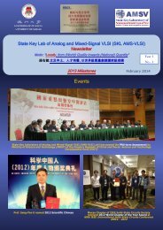
Events<br />
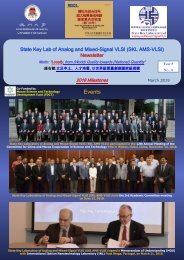
A delegation led by Wan Gang, Vice Chairman of the Chinese People’s Political Consultative Conference and Minister<br />
of Science and Technology, visited the University of Macau’s (UM) State Key Laboratory of Analog and Mixed-Signal<br />
VLSI (SKL AMS-VLSI) on 4 December <strong>2015</strong><br />
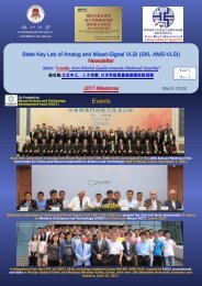
FDCT/MOST Annual Meeting in Chengdu, China, Chaired by Cao Jianlin, Vice-Minister of Science & Technology on<br />
November <strong>2015</strong><br />
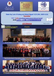
The University of Macau’s (UM) State Key Laboratory of Analog and Mixed-Signal VLSI (SKL AMS-VLSI) held in<br />
April <strong>2015</strong> the 2nd meeting of the Academic Committee, which summarized and analyzed the lab current status,<br />
and gave great recognition to <strong>AMSV</strong>’s development direction
State-of-the-Art Chips - Designed and Tested in <strong>2015</strong> (20 chips)<br />
A successfully<br />
developed power<br />
quality compensator<br />
ISSCC 2016<br />
Four PhD students and one assistant professor from the University of Macau (UM) State Key Laboratory of Analog and Mixed-Signal<br />
VLSI (AMS-VLSI Lab) and Faculty of Science and Technology attended the Institute of Electrical and Electronics Engineer’s (IEEE)<br />
62 nd International Solid-State Circuits Conference (ISSCC) in February 2016, which is considered the ‘Chip Olympics’, the<br />
most competitive conference in the field of chip design.<br />
The 3 papers and 3 Student Research Previews from UM<br />
were "A 0.038mm 2 Saw-less Multiband Transceiver using an N-Path SC<br />
Gain Loop", "A 0.003mm 2 1.7-to-3.5GHz Dual-Mode Time-Interleaved<br />
Ring-VCO achieving 90-to150kHz 1/f3 Phase-Noise Corner", "A<br />
Handheld 50-pM Sensitivity Micro-NMR CMOS Platform with B-Field<br />
Stabilization for Multi-Type Biological/Chemical Assays", "A 12.5-ENOB<br />
5MHz BW 4.2mW DT Multirate 2-1 Mash ΔΣ Modulator with Horizontal/<br />
Vertical Opamp Sharing in 65nm CMOS", "A 0.45V 147-to-375nW<br />
Hardware-Efficient Real-Time ECG Processor with Lossless-to-Lossy<br />
Data Compression for Wireless Healthcare Wearables", and "A 2.4-GHz<br />
Digitally-Modulated Class-D Polar PA Using Power-Gating, Interactive<br />
AM-AM Modulation and a Dynamic Matching Network for Battery Lifetime<br />
Extension". There included 1 Silk Road Award and 2 Student<br />
Travel Grant Awards.<br />
Prof. Seng-Pan U becomes the 1st<br />
Macao-educated scholar to be<br />
elevated to IEEE fellow<br />
A research team from SKL AMS-VLSI<br />
received the Best Paper Award at<br />
ESSCIRC <strong>2015</strong><br />
UM PhD student receives<br />
Distinguished Design Award at<br />
IEEE A-SSCC <strong>2015</strong><br />
Prof Seng-Pan U who is the deputy director of<br />
the State Key Laboratory of Analog and<br />
Mixed-Signal VLSI, has been elevated to the<br />
fellowship of the IEEE for the year 2016,<br />
becoming the first scholar who was educated<br />
in Macao, who has developed his professional<br />
career both at UM and in the local and global<br />
electronics industry, to be elevated to this<br />
prestigious fellowship. Prof U was nominated<br />
by IEEE Solid-State Circuit Society Presidentelect<br />
Prof Jan Van Spiegel, for leadership in<br />
the analog circuit design.<br />
A research team from the University of<br />
Macau (UM) received the Best Paper Award<br />
at the European Solid-State Circuits Conference<br />
(ESSCIRC) <strong>2015</strong>, which is considered<br />
‘Europe’s “Chip Olympics”’. This year’s conference<br />
attracted 200 high-quality papers<br />
from all over the world. The UM team was<br />
composed by assistant professor Zhu Yan<br />
and PhD student Chan Chi Hang from SKL<br />
AMS-VLSI; Prof. U Seng Pan from the Department<br />
of Electrical and Computer Engineering,<br />
Faculty of Science and Technology;<br />
and Vice Rector (Research) Prof. Rui Martins,<br />
both also from SKL AMS-VLSI.<br />
Lei Ka-Meng, a PhD student from the University<br />
of Macau (UM) SKL AMS-VLSI and<br />
Faculty of Science and Technology (FST),<br />
recently received a Distinguished Design<br />
Award for his research paper titled “A µNMR<br />
CMOS Transceiver Using a Butterfly-Coil<br />
Input for Integration with a Digital Microfluidic<br />
Device Inside a Portable Magnet” at<br />
the IEEE Asian Solid-State Circuits Conference<br />
<strong>2015</strong> (IEEE A-SSCC <strong>2015</strong>).<br />
4 New PhD Graduates<br />
4. Jie Gao, Electronic-Automated Intelligent Digital Microfluidic System and Its Applications to DNA Amplification, Oct. <strong>2015</strong>.<br />
3. Chi-Hang Chan, Design Techniques and Considerations in Low-to-moderate Resolution Power-efficient GHz Range ADCs, Jul. <strong>2015</strong>.<br />
2. Yaohua Zhao, Low-Power High-Linearity and Area-Efficient Switched-Capacitor Filters Design Techniques in Nanoscale CMOS, Mar. <strong>2015</strong>.<br />
1. Tawfiq Amin, Analysis and Design of Power-Efficient Voltage-Controlled Oscillators for Wireless Applications in Nanoscale CMOS, Mar. <strong>2015</strong>.<br />
US Patents granted in <strong>2015</strong><br />
1. Ka-Fai Un, Pui-In Mak, R.P.Martins, “Wideband Driver Amplifier”, US Patent, No. 9,172,337, Oct. <strong>2015</strong>.<br />
2. Chi-Seng Lam, Man-Chung Wong, Wai-Hei Choi, Ying-Duo Han, “Adaptive DC-link voltage controlled LC coupling hybrid active<br />
power filters for reactive power compensation”, US Utility Patent, Granted, No. 9,122,296, Sep. <strong>2015</strong>.<br />
3. Ka-Fai Un, Pui-In Mak, Man-Kay Law, R.P.Martins, “Poly-phase Local Oscillator”, No. 9,093,951, US Patent, Jul. <strong>2015</strong>.<br />
4. Ka-Fai Un, Pui-In Mak, Man-Kay Law, R.P.Martins, “Wireless Transmitter”, No. 9,037,100, US Patent, May <strong>2015</strong>.<br />
5. Yan Zhu, Chi-Hang Chan, Sai-Weng Sin, Seng-Pan U, R.P.Martins, “Sampling front-end for analog to digital converter”, No.<br />
8,947,283, US Patent, Feb. <strong>2015</strong>.<br />
6. Zushu Yan, Pui-In Mak, Man-Kay Law and R. P. Martins, “Frequency Compensation Techniques for Low-Power and Small-Area<br />
Multistage Amplifiers”, No. 8,963,639, US Patent, Feb. <strong>2015</strong>.
Selected works from each research line<br />
In JSCC <strong>2015</strong><br />
A 0.02-mm 2 59.2-dB SFDR 4th-Order SC LPF With 0.5-to-10 MHz<br />
Bandwidth Scalability Exploiting a Recycling SC-Buffer Biquad<br />
Yaohua Zhao, Pui-In Mak, Rui P. Martins and Franco Maloberti<br />
From Wireless research line<br />
Motivation<br />
Architecture<br />
This work is a switched-capacitor (SC)-buffer Biquad<br />
that can be recycled efficiently as an ultra-compact<br />
low-pass filter (LPF) in nanoscale CMOS. It incorporates<br />
only passive-SC networks and open-loop unitygain<br />
buffers; both are friendlier to technology<br />
downscaling than most conventional Biquads that<br />
use high-gain amplifiers and closed-loop negative<br />
feedback. Complex-pole pairs with independent Q<br />
factors are recursively realized in one clock period,<br />
while ensuring low crosstalk effect between the formations<br />
of each pole. Nonlinearity and parasitic effects<br />
are inherently low due to no internal gain. The<br />
fabricated 65 nm CMOS prototype is a 1x-recycling<br />
SC-buffer Biquad that is equivalent to a 4th-order<br />
Butterworth LPF with 75% buffer utilization. It occupies<br />
a die size of only 0.02 mm and exhibits 20x<br />
bandwidth tunability (0.5 to 10 MHz), linear with the<br />
clock rate. At 10 MHz bandwidth, the in-band IIP3 is<br />
+17.6 dBm and input-referred noise is 19.5 nV/ Hz;<br />
they correspond to 59.2 dB SFDR and 0.013 fJ figure<br />
-of-merit which are favorably comparable with the<br />
recent art. The 1 dB compression point conforms to<br />
the out-of-band blocker profile of the LTE standard at<br />
a 20 dB front-end gain.<br />
Implementation<br />
Verification
Adhesion Promoter for a Multi-Dielectric-Layer on a Digital<br />
Microfluidic Chip<br />
Jie Gao, Tianlan Chen, Cheng Dong, Yanwei Jia, Pui-In Mak, Mang-I Vai,<br />
and Rui P. Martins<br />
From Multidisciplinary Research Area (Microfluidic)<br />
In UK Royal Society of Chemistry – Advances <strong>2015</strong><br />
Motivation<br />
Technique<br />
A silane-based adhesion promoter suitable<br />
for a multi-dielectric-layer coating on a digital<br />
microfluidic chip is reported.<br />
It measures >100 improvement in chip lifetime<br />
via transforming the bonding of the dielectric<br />
layers (Ta 2 O 5 and Parylene C) from<br />
nonspecific to chemical.<br />
The refined chip-fabrication protocol also<br />
allows low EWOD actuation voltages down<br />
to 5 V.<br />
Verification I<br />
Verification II
In IEEE Transactions on Electron Devices <strong>2015</strong><br />
A Precision CMOS Voltage Reference Exploiting Silicon Bandgap<br />
Narrowing Effect<br />
Bo Wang, Man-Kay Law and Amine Bermak<br />
From Wireless research line<br />
Motivation<br />
Architecture<br />
Conventional precision voltage references<br />
(BGRs) can be achieved by multiple temperature<br />
trimmings and/or power hungry curvature<br />
correction circuits that inevitably increases cost<br />
and energy efficiencies. We exploit the intrinsic<br />
temperature characteristics of the BJT itself to<br />
reduce the BJT curvature and perform curvature<br />
correction using the silicon bandgap narrowing<br />
effect so as to avoid the power overhead of curvature<br />
correction circuits by batch trimming.<br />
Measurement results show that the BJT curvature<br />
can be effectively reduced from its inherent<br />
3.6 mV to 1.4 mV. The proposed BGR measures<br />
a minimum temperature coefficient of 8.7 ppm/°<br />
C and 4.1 ppm/°C from −55 °C to 125 °C after<br />
batch trimming and curvature trimming, respectively.<br />
Proposed BGR Topology with curvature reduction using bandgap<br />
narrowing effect<br />
Relationship between voltage and temperature showing the curvature reduction<br />
and correction with convex (left) and concave (right) BJT intrinsic curvatures.<br />
Implementation<br />
Verification<br />
(a)<br />
Complete schematic of the proposed BGR using bandgap narrowing effect.<br />
(b)<br />
Chip micrograph of the proposed BGR<br />
(a) Inaccuracy of V REF from 12 samples without trimming and after batch<br />
trimming resistor R c1 at 25 °C (dotted lines indicates ± 3σ values); (b)<br />
Measured BJT intrinsic curvature and V REF before and after the curvature<br />
compensation.
In IET Electronics Letters <strong>2015</strong><br />
Output pressure enhancement of CMUTs by using multiple<br />
Helmholtz resonance apertures<br />
Yuan Yu Yu, Xue Wen Cao, Sio Hang Pun, Peng Un Mak and Mang I Vai<br />
From Biomedical IC research line<br />
Motivation<br />
Architecture<br />
Multiple Helmholtz resonance apertures are proposed<br />
to enhance the output pressure of aircoupled<br />
capacitive micromachined ultrasonic<br />
transducers (CMUTs) for non-contact ultrasound<br />
imaging applications.<br />
The methodologies of defining the design parameters<br />
of CMUTs and the resonant apertures<br />
on the membrane of CMUTs are discussed.<br />
In comparing certain configurations of resonant<br />
apertures with conventional CMUTs, simulation<br />
results show that a prospective improvement of<br />
output pressure (up to 32.1%) can be achieved.<br />
Cross-section view of CMUT cell with Helmholtz resonance<br />
apertures (red dash line indicates central axis of CMUT cell<br />
(not in scale))<br />
Implementation<br />
Verification<br />
3D FEA model of CMUT cell and air domain: CMUT cell and<br />
air domain (Fig. a) and details of CMUT cell (Fig. b)<br />
Cross-section view of CMUT cell with Helmholtz resonance<br />
apertures (red dash line indicates central axis of CMUT cell<br />
(not in scale))
In ESSCIRC 2014 & JSSC 2016<br />
An 11b 450 MS/s 3-way Time-Interleaved Sub-ranging Pipelined-<br />
SAR ADC in 65nm CMOS<br />
Yan Zhu, Chi-Hang Chan, Seng-Pan (Ben) U, and Rui Paulo Martins<br />
From Data Conversion and Signal Processing research line<br />
Motivation<br />
Architecture<br />
The SAR architecture demands a stringent noise requirement<br />
for the comparator design while aiming for<br />
high resolution.<br />
The mismatch spurs due to the timing, offset and<br />
gain in TI SAR limit both signal-to-noise distortion<br />
ratio (SNDR) and spurious-free dynamic range<br />
(SFDR).<br />
The pipelined-SAR ADCs still maintain their superiority<br />
in power efficiency with high resolution in deep<br />
sub-micron technology. The implementation of low<br />
stage-gain (G) relaxes the desired noise requirement<br />
in the comparator and balances the trade-off between<br />
the power dissipation and gain-bandwidth<br />
product (GBW) requirement of the Op-Amp.<br />
Time skews on the other hand are tolerated by design<br />
constraint or avoided through architecture optimizations.<br />
Proposed hybrid ADC architecture and multiple<br />
shared elements among the TI channels.<br />
Implementation<br />
Verification
A 6 b 5 GS/s 4 Interleaved 3 b/Cycle SAR ADC<br />
In ISSCC <strong>2015</strong> & JSSC 2016<br />
Chi-Hang Chan, Yan Zhu, Sai-Weng Sin, Seng-Pan (Ben) U, and Rui Paulo Martins<br />
From Data Conversion and Signal Processing research line<br />
Motivation<br />
Architecture<br />
For 60GHz-band receivers and serial links applications.<br />
The SAR ADC is a well-known energy-efficient architecture<br />
while the speed of SAR ADCs can be further improved<br />
with the comparator interleaving, loop-unrolled<br />
asynchronous loop or the multi-bit per cycle.<br />
The Flash ADC is known as the fastest ADC architecture<br />
but power hungry. By adopting interpolation or calibration,<br />
outstanding energy efficiency can also be accomplished<br />
under advanced technology nodes.<br />
In a standalone flash or SAR architecture, speed and<br />
energy efficiency are still limited due to their inherent<br />
characteristics; therefore, they are often combined with<br />
time interleaving to achieve a breakthrough.<br />
Time interleaving can be a very effective way to increase<br />
the sampling rate of the ADC but it induces extra design<br />
complexity and conversion non-idealities especially with<br />
large numbers of interleaving channels.<br />
V in,P<br />
V in,N<br />
Input<br />
4<br />
En, chX<br />
4×<br />
Channels<br />
Clock<br />
Gen.<br />
Common<br />
Clk<br />
Bootstrap<br />
2<br />
V ref,N/V ref,P<br />
Decoder & BDCO<br />
3b/cycle SAR<br />
Segmentation Logic<br />
8<br />
DAC Array<br />
DAC Array<br />
DAC Array<br />
DAC Array<br />
Dummy Latch<br />
Dynamic<br />
Pre-amp.<br />
interpolation<br />
Latch<br />
Latch<br />
Latch<br />
Latch<br />
Latch<br />
Latch<br />
Latch<br />
Latch<br />
On-Chip Offset Calibration Cal Ctrl.<br />
6<br />
14<br />
6<br />
MUX<br />
Final Output<br />
Codes<br />
The power required for the digital gain and timing corrections<br />
is prohibitive at 6b resolution.<br />
Implementation<br />
Verification<br />
40<br />
30<br />
20<br />
10<br />
0<br />
SNDR/SFDR (dB)50<br />
43.5<br />
30.78<br />
SFDR<br />
SNDR @Nyquist<br />
43.12<br />
30.76<br />
42.95<br />
30.66<br />
1 2 3<br />
#Sample<br />
Sample #2, fs = 5 Gs/s<br />
45<br />
SNDR/SFDR (dB)<br />
40<br />
35<br />
30<br />
25<br />
SFDR<br />
SNDR<br />
20<br />
0 0.5 1.0 1.5 2.0 2.5 3.0<br />
Input Frequency (GHz)<br />
ISSCC’10[1] VLSI’13[5] VLSI’12[6] ISSCC’14[25] A-SSCC’14[26] This work<br />
Architecture Ti-pipelined B-S Flash Flash Ti-SAR Ti-SAR Ti-Multi-bit SAR<br />
Process 40nm 32nm SOI 40nm 28nm UTBB FDSOI 32nm SOI<br />
65nm<br />
Supply voltage (V) 1.1 0.85 1.1 1.0<br />
1.1 1.0 1.2<br />
10<br />
36<br />
5 6<br />
Sampling rate (GS/s) 2.2 5<br />
3<br />
Resolution (bit) 6 6<br />
Power (mW) 2.6 11<br />
SNDRminin Nyq. band (dB) 29.6 33.1<br />
Input cap.(fF) 200 72<br />
FoM@ Nyq.(fJ/conv.-step) 40.0 100.48<br />
Active area (mm 2 ) * 0.03 * 0.02 * 0.021<br />
Calibration<br />
Off-chip Off-chip Off-chip<br />
*without Calibration **with Calibration<br />
6 6<br />
6<br />
6<br />
8.5 32<br />
110 5.5 10.6<br />
30.9 33.8<br />
31.6 30.25 30.13<br />
135 100<br />
N/A<br />
31<br />
59.33 81<br />
98<br />
39 67.37<br />
* 0.009 ** 0.048 * 0.008 (**<br />
0.09)<br />
Off-chip On-chip<br />
On-chip
A Digital Low-Dropout Regulator with Coarse-Fine-Tuning and<br />
Burst-Mode Operation<br />
Mo Huang, Yan Lu, Sai-Weng Sin, Seng-Pan U, and Rui P. Martins<br />
In TCAS-II 2016<br />
[Accepted in <strong>2015</strong>]<br />
From Integrated Power research line<br />
Motivation<br />
Digital low-dropout (D-LDO) regulator, that replaces the<br />
power transistor in analog LDO regulator with a power<br />
switch array, has recently drawn significant attention for<br />
its low operation voltage and process scalability feature.<br />
However, for a conventional shift register based D-LDO,<br />
only one PMOS is turned on/off per clock cycle for the<br />
shift register operation; and the transient speed can only<br />
be improved by increasing sampling frequency which<br />
degrades the power consumption. To address this issue,<br />
a wide load range D-LDO regulator with coarse-fine tuning<br />
and burst-mode techniques is proposed for fast transient<br />
response and low quiescent current.<br />
Architecture<br />
For the proposed topology, the PMOS arrays consist of one<br />
coarse section and one fine section, driven by separate shift<br />
registers. To extend the load current range, the coarse<br />
PMOS array is designed to be with 64 power switches. The<br />
unit size of the coarse PMOS is designed to be 16 times of<br />
that of the fine PMOS for the loop gain boosting. To cover<br />
the current gap between two adjacent coarse bits can provide,<br />
the fine PMOS array is designed with 32 units for sufficient<br />
margin. Once the voltage undershoot/overshoot is<br />
detected, the coarse-tuning quickly finds out the coarse control<br />
word in which the load current should be located, with<br />
large power MOS strength and high sampling frequency for<br />
a fixed duration. Then, the fine-tuning with reduced power<br />
MOS strength and sampling frequency takes over the<br />
steady-state operation for high accuracy and current efficiency.<br />
Implementation<br />
Verification<br />
The proposed D-LDO regulator was fabricated in a 65-nm<br />
CMOS process.
Sensor<br />
Conventional<br />
Proposed<br />
Conventional<br />
Proposed<br />
In TPEL <strong>2015</strong><br />
Self-reconfiguration property of a mixed signal controller for<br />
improving power quality compensator during light loading<br />
Man-Chung Wong, Yan-Zheng Yang, Chi-Seng Lam, Wai-Hei Choi, Ning-Yi Dai, Ya-jie Wu,<br />
Chi-Kong Wong, Sai-Weng Sin, U-Fat Chio, Seng-Pan U, R.P. Martins<br />
From Integrated Power research line<br />
Motivation<br />
Currently, when compensator performance<br />
does not satisfy international standards, other<br />
PWMs can be selected, or the dc link voltage<br />
can be increased. However, it may be the case<br />
that neither of these methods will improve compensator<br />
performance during light loading due<br />
to the low resolution of the input signals compared<br />
with the error signal and the PWM error<br />
margin. The design of digital controllers is usually<br />
based on a full loading situation. The full<br />
analog-to-digital (A/D) conversion input signal<br />
range of a digital controller is therefore utilized,<br />
to avoid analog signal saturation. In a light load<br />
situation, the digital controller may suffer from<br />
the problem of low resolution, which significantly<br />
affects its compensation performance. There<br />
is presently no achievable control strategy to<br />
deal with power quality compensation issues<br />
during light loading.<br />
Architecture<br />
A mixed signal controller for power quality compensator is proposed for enhancing<br />
the advanced performance that cannot be achieved by analog or<br />
digital controller alone and independently. Several special features can be<br />
achieved by mixed signal controller are given as follows:<br />
▓ Adaptive Signal Conditioning and Programmability on-the-Fly<br />
▓ Parallelism Properties and Higher Redundancy<br />
▓ Higher Accuracy, Higher Bandwidth, Faster Response Time and Low<br />
Power<br />
▓ Algorithm Complexity and Simplicity of Implementation<br />
The FPAA can be operated as an adaptive signal conditioning unit that preconditions<br />
and filters, according to the optimization of system performance.<br />
The modified signals then pass to the digital unit for further processing, assisted<br />
by the ADC. The digital system, FPGA/DSP, can work with a “backer”<br />
sub-program to optimize the system operation by reconfiguring the control<br />
system automatically, or to carry out self-testing and self-repairing tasks.<br />
When it is necessary to reconfigure the analog part, the re-programming data<br />
can be transferred directly through the digital path to the FPAA. Conversely,<br />
the FPAA can also send out control signals to the FPGA to modify the algorithm<br />
for protection, critical operations, etc.<br />
Input Signals<br />
vLa, vLb, vLc<br />
iLa, iLb, iLc<br />
iCa, iCb, iCc<br />
FPAA<br />
Mixed Signal Controller<br />
vLa, vLb, vLc<br />
iLa, iLb, iLc<br />
iCa, iCb, iCc<br />
Gain Saturation<br />
Signal<br />
ADC<br />
Reconfigurable<br />
Gain G<br />
FPGA/<br />
DSP<br />
PWM Signals<br />
Ta,Ta<br />
Tb,Tb<br />
Tc,Tc<br />
Analog Signal Paths<br />
Digital Signal Paths<br />
Implementation<br />
Verification<br />
The proposed mixed signal controller is tested in a threephase<br />
four-wire hybrid active power filter (HAPF) system in<br />
comparison with a conventional digital controller.<br />
v sa<br />
v sb<br />
L s<br />
i sn<br />
i sb<br />
i sc<br />
v La<br />
v Lb<br />
v Lc<br />
ica<br />
icb<br />
icc<br />
i La<br />
i Lb<br />
i Lc<br />
A<br />
B Loads N<br />
C<br />
i Ln<br />
A<br />
N<br />
B<br />
N<br />
C<br />
N<br />
LLa<br />
LLb<br />
LLc<br />
RLa<br />
RLb<br />
RLc<br />
Inductive<br />
Linear Load<br />
IEEE Standard (
Events and Visits<br />
Visit by Mr. Ma Chi Ngai Frederico, President of FDCT<br />
with members of S&T Assessment Committee (FDCT)<br />
Visit by Dr. Peter Lam, University Council Chair<br />
Distinguished Lectures on Microelectronics<br />
Distinguished Lecture on Microelectronics - "Power Minimization in<br />
Amplifiers and Filters" by Prof. Willy Sansen , IEEE Life Fellow,<br />
Professor at the Catholic University of Leuven, in Belgium<br />
Distinguished Workshop on Analog IC Design by<br />
Professor Behzad Razavi, Professor of electrical engineering at<br />
University of California, Los Angeles, USA<br />
4 New Academics, 1 Post-Doc and 1 Administrative Joined SKL AMS-VLSI<br />
Assistant Professor<br />
Yanwei Jia, received the B.S. and M. S degrees from Hunan University, Changsha, China in 1996 and 2002, respectively, and the Ph.D.<br />
degree from the National University of Singapore in 2006. She currently serves as assistant professor at SKL AMS-VLSI.<br />
Research interests: Microfluidics, Biotechnology and Multidisciplinary research.<br />
Assistant Professor<br />
Yong Chen, received the B.Eng. degree in electronic and information engineering, Communication University of China (CUC), Beijing,<br />
China, in 2005, and the Ph.D. in Engineering in microelectronics and solid-state electronics, Institute of Microelectronics of Chinese<br />
Academy of Sciences (IMECAS), Beijing, China, in 2010. He currently serves as assistant professor at SKL AMS-VLSI.<br />
Research Interests: Analog/Biomedical detection and RF integrated circuit, mm-wave system and circuit, high-speed on-chip and chip-to<br />
-chip Electrical/Optical<br />
Research Assistant Professor<br />
Chi-Hang Chan received the B.S. degree in electrical engineering from University of Washington (U.W. Seattle), USA, in 2008, and the<br />
M.S. degree in electrical and electronics engineering and Ph.D. degree from the University of Macau, Macao, China, in 2012 and <strong>2015</strong>,<br />
respectively. He currently serves as research assistant professor at SKL AMS-VLSI.<br />
Research interests: Nyquist ADC, Mixed-signal circuits.<br />
Lecturer (Macao Fellow)<br />
Ka-Fai Un received the B.Sc. degree in electrical engineering from National Taiwan University (NTU), Taipei, Taiwan, in 2007, and the<br />
M.Sc. degree in electrical and electronics engineering and Ph.D. degree from the University of Macau (UM), Macao, China, in 2009 and<br />
2014, respectively. He is currently a lecturer (Macao Fellow) at SKL AMS-VLSI.<br />
Research Interests: Wireless integrated circuits design, Mathematics.<br />
Post-Doctoral Fellow & Cleanroom Specialist<br />
Jie Gao, she received her M.Sc. degree in Materials Science and Engineering from the Technical University of Hamburg-Harburg,<br />
Germany and University of Aveiro, Portugal in 2007. She received her Ph.D. degree in Electrical and Computer Engineering from University<br />
of Macau, in <strong>2015</strong>. She currently serves as Post-Doctoral Fellow and Cleanroom Specialist at SKL AMS-VLSI.<br />
Research interests: Design and fabrication of automated microfluidic chips for point-of-care applications.<br />
Senior Administrative Officer<br />
Weng-Keong CHE received the B.S. degree, M.S. degree and Ph.D. degree from the National Taiwan University, in 1997, 1999 and<br />
2005, respectively. He currently serves as Senior Administrative Officer for commercialization coordination, industrial collaboration and<br />
spin-off incubation at SKL AMS-VLSI.<br />
Research interests: RF Transceiver IC / RF SoC / Fiber optical Front-End IC / MCU SoC / Automobile SoC design.
SCI Journals – 28 Papers<br />
▓ “Polyphase Decomposition for Tunable Band-Pass Sigma-Delta A/D Converters”, IEEE Journal on Emerging and Selected Topics in Circuits and<br />
Systems, Dec. <strong>2015</strong>.<br />
▓ “Energy Optimized Subthreshold VLSI Logic Family With Unbalanced Pull-Up/Down Network and Inverse Narrow-Width Techniques”, IEEE Transactions<br />
on VLSI Systems, Dec. <strong>2015</strong>.<br />
▓ “Improving the Linearity and Power Efficiency of Active Switched-Capacitor Filters in a Compact Die Area”, IEEE Transactions on VLSI Systems, Dec.<br />
<strong>2015</strong>.<br />
▓ “DCM operation analysis of KY converter”, IET Electronics Letters, Nov. <strong>2015</strong><br />
▓ “Non-Linear adaptive hysteresis band pwm control for hybrid active power filters in reducing switching loss”, IET Power Electronics, Nov. <strong>2015</strong><br />
▓ "Nested-Current-Mirror Rail-to-Rail-Output Single-Stage Amplifier With Enhancements of DC Gain, GBW and Slew Rate", IEEE Journal of Solid-State<br />
Circuits, Oct. <strong>2015</strong><br />
▓ "A Sub-GHz Wireless Transmitter Utilizing a Multi-Class-Linearized PA and Time-Domain Wideband-Auto I/Q-LOFT Calibration for IEEE 802.11af WLAN",<br />
IEEE Transactions on Microwave Theory and Techniques, Oct. <strong>2015</strong><br />
▓ “Self-reconfiguration property of a mixed signal controller for improving power quality compensator during light loading,” IEEE Transactions on Power<br />
Electronics, Oct. <strong>2015</strong><br />
▓ “Hybrid railway power conditioner with partial compensation for converter power rating reduction”, IEEE Transactions on Industry Applications,<br />
Sep./Oct. <strong>2015</strong><br />
▓ "A 0.02 mm 59.2 dB SFDR 4th-Order SC LPF With 0.5-to-10 MHz Bandwidth Scalability Exploiting a Recycling SC-Buffer Biquad", IEEE Journal of Solid-<br />
State Circuits, Sep. <strong>2015</strong><br />
▓ "Thermal and Reference Noise Analysis of Time-Interleaving SAR and Partial-Interleaving Pipelined-SAR ADCs," IEEE Transactions on Circuits and<br />
Systems-I: Regular Papers, Sep. <strong>2015</strong><br />
▓ "Resolution-enhanced sturdy MASH delta–sigma modulator for wideband low-voltage applications", IET Electronics Letters, Jul. <strong>2015</strong><br />
▓ "A CMOS Delta-Sigma PLL Transmitter with Efficient Modulation Bandwidth Calibration," IEEE Transactions on Circuits and Systems-I: Regular<br />
Papers, Jul. <strong>2015</strong><br />
▓ “A Precision CMOS Voltage Reference Exploiting Silicon Bandgap Narrowing Effect”, IEEE Transactions on Electron Devices, Jul. <strong>2015</strong><br />
▓ “A 0.07mm 2 2.2 mW 10 GHz Current-Reuse Class-B/C Hybrid VCO achieving 196-dBc/Hz FoM A ”, IEEE Microwave Wireless and Components Letters,<br />
Jul. <strong>2015</strong>.<br />
▓ "A Palm-Size µNMR Relaxometer Using a Digital Microfluidic Device and a Semiconductor Transceiver for Chemical/Biological Diagnosis", Royal Society of<br />
Chemistry - Analyst, Jun. <strong>2015</strong><br />
▓ “Analysis, control and experimental verification of a single-phase capacitive-coupling grid connected inverter”, IET Power Electronics, May <strong>2015</strong><br />
▓ "Adhesion Promoter for Multi-dielectric-layer on Digital Microfluidic Chip", RSC Advances, May <strong>2015</strong><br />
▓ "A Highly-Scalable Analog Equalizer Using a Tunable and Current-Reusable Active Inductor for 10-Gb/s I/O Links", IEEE Transactions on VLSI Systems,<br />
May <strong>2015</strong><br />
▓ "On the Droplet Velocity and Electrode Lifetime of Digital Microfluidics: Voltage Actuation Techniques and Comparison", Springer Microfluidics and<br />
Nanofluidics, Apr. <strong>2015</strong><br />
▓ "A Combinatorial Impairment-Compensation Digital Predistorter for a Sub-GHz IEEE 802.11af-WLAN CMOS Transmitter Covering a 10x-Wide RF Bandwidth",<br />
IEEE Transactions on Circuits and Systems–I: Regular Papers, Apr. <strong>2015</strong><br />
▓ “Output pressure enhancement of CMUTs by using multiple Helmholtz resonance apertures,” IET Electronics Letters, Mar. <strong>2015</strong><br />
▓ "A 0.0045-mm 2 32.4-µW Two-Stage Amplifier for pF-to-nF Load Using CM Frequency Compensation", IEEE Transactions on Circuits and Systems–II:<br />
Express Briefs, Mar. <strong>2015</strong><br />
▓ " 0.0045mm 2 15.8μW Three-Stage Amplifier Driving 10x-Wide (0.15 to 1.5nF) Capacitive Loads with >50° Phase Margin", IET Electronics Letters, Mar.<br />
<strong>2015</strong><br />
▓ "Wideband Receivers: Design Challenges, Tradeoffs and State-of-the-Art", IEEE Circuits and Systems Magazine, Mar. <strong>2015</strong><br />
▓ "A Fully-Integrated Low-Dropout Regulator with Full-Spectrum Power Supply Rejection," IEEE Transactions on Circuits and Systems-I: Regular<br />
Papers, Mar. <strong>2015</strong><br />
▓ “A systematic approach to hybrid railway power conditioner design with harmonic compensation for high-speed railway”, IEEE Transactions on Industrial<br />
Electronics, Feb. <strong>2015</strong><br />
▓ "A 3.6mW 6GHz Current-Reuse VCO-Buffer with Improved Load Drivability in 65nm CMOS", Wiley International Journal of Circuit Theory and<br />
Applications, Jan. <strong>2015</strong><br />
Conferences – 23 Papers<br />
Major IEEE solid-state circuits conferences<br />
IEEE International Solid-State Circuits Conference (ISSCC) <strong>2015</strong>, San Francisco, CA, USA, Feb. <strong>2015</strong><br />
▓ “A 5.5mW 6b 5GS/s 4-times Interleaved 3b/cycle SAR ADC in 65nm CMOS” [Pre-Doctoral Achievement Award]<br />
▓ “A 0.028mm 2 11mW Single-Mixing Blocker-Tolerant Receiver with Double-RF N-Path Filtering, S 11 Centering, +13dBm OB-IIP 3 and 1.5-to-2.9dB NF” [Pre-<br />
Doctoral Achievement Award]<br />
▓ “A 123-Phase DC-DC Converter-Ring with Fast-DVS for Microprocessors”<br />
▓ “A 2-/3-Phase Fully-Integrated Switched-Capacitor DC-DC Converter in Bulk-CMOS for Energy-Efficient Digital Circuits With 14% Efficiency Improvement”<br />
▓ “A 12b 180MS/s 0.068mm 2 Full-Calibration Integrated Pipelined-SAR ADC” [Student Research Preview]<br />
▓ “A Multi-Step Multi-Sample µNMR Relaxometer Using Inside-Magnet Digital Microfluidics and a Butterfly-Coil-Input CMOS Transceiver” [Student Research<br />
Preview]<br />
IEEE Asian Solid-State Circuits Conference (A-SSCC), Xiamen, Fujian, China, Nov. <strong>2015</strong><br />
▓ “A μNMR CMOS Transceiver Using a Butterfly-Coil Input for Co-integration with a Digital Microfluidic Device Inside a Portable Magnet” [Distinguished<br />
Design Award]<br />
▓ “A 89fJ-FOM 6-bit 3.4GS/s flash ADC with 4x time-domain interpolation”<br />
Other IEEE conferences:<br />
IEEE Region 10 Conference (TENCON), Macao, China, Nov. <strong>2015</strong><br />
▓ “An All-Factor Modulation Bandwidth Extension Technique for Delta-Sigma PLL Transmitter” [Professional Award]<br />
▓ “Capacitive floating level shifter: Modeling and design”<br />
▓ “Generalized type III controller design interface for dc-dc converters”<br />
▓ “Hardware and software design of a thyristor controlled LC-coupling hybrid active power filter”<br />
▓ “Comparison among PPF, APF, HAPF and a combined system of a shunt HAPF and a shunt thyristor controlled LC”<br />
▓ “A woman in engineering - increasing Macao students’ interest in science and technology” [Invited Workshop Paper]<br />
▓ “Historical review of hybrid active power filter for power quality improvement”<br />
International Conference on Miniaturized Systems for Chemistry and Life Sciences (MicroTAS), Gyeongju, Korea, Oct. <strong>2015</strong><br />
▓ “A Thermal-Insensitive All-Electronic Modular µNMR Relaxometer with a 2D Digital Microfluidic Chip for Sample Management”<br />
IEEE Energy Conversion Congress and Exposition (ECCE), Montreal, Canada, Sep. <strong>2015</strong><br />
▓ “Analysis, design and implementation of a quasi-proportional-resonant controller for multi-functional capacitive-coupling grid-connected inverter”<br />
IEEE Ph.D. Research In Micro-electronics and Electronics (PRIME), Glasgow, Scotland, Jul. <strong>2015</strong><br />
▓ “Exploring the Noise Limits of Fully-Differential Micro-Watt Transimpedance Amplifiers for Sub-pA/√Hz Sensitivity”<br />
International Symposium on Signals, Circuits and Systems (ISSCS), Iasi, Romania, Jul. <strong>2015</strong><br />
▓ “Multi-Range, Ultra-Low-Power, -20 to 60°C CMOS Smart Temperature Sensor with ±0.1°C Inaccuracy”<br />
▓ “Comparator with Built-in Reference Voltage Generation and Split-ROM Encoder for a High-Speed Flash ADC”<br />
IEEE Congress on Evolutionary Computation (CEC), Sendai, Miyagi, Japan, May <strong>2015</strong><br />
▓ “Predicting Protein Docking Poses on a Solid Surface by Particle Swarm Optimization”<br />
IEEE EMBS Neural Engineering Conference (NER), Montpellier, France, Apr. <strong>2015</strong><br />
▓ “Input Capacitance Compensated Neural Recording Amplifier”<br />
IEEE International Wireless Symposium (IWS), Shenzhen, China, Mar. <strong>2015</strong><br />
▓ “A Review and Design of the On-Chip Rectifiers for RF Energy Harvesting”<br />
State Key Laboratory of Analog and Mixed-Signal VLSI / UM<br />
http://www.amsv.umac.mo