

Deliverables and Services - IHP Microelectronics
Deliverables and Services - IHP Microelectronics
Deliverables and Services - IHP Microelectronics

Create successful ePaper yourself
Turn your PDF publications into a flip-book with our unique Google optimized e-Paper software.
2 A n n u A l R e p o R t 2 0 0 9<br />
A u S G e w ä H L t e p r o J e K t e – S e L e C t e d p r o J e C t S<br />
Gitter sind häufig zur Kopplung von Licht in Nanowellenleiter<br />
eingesetzte Komponenten. Eine solche Koppelgitterstruktur<br />
ist in Abb. 25 gezeigt. Es wurden einfache<br />
1D-Gitterkoppler mit einem flachen Siliziumätz<br />
hergestellt (70 nm), wobei die nominale Dicke des SOI<br />
220 nm beträgt. Die Nanowellenleiterverluste bewegen<br />
sich im Bereich 4 dB/cm. Einfache 1D-Koppler wiesen<br />
Verluste von -7 dB auf.<br />
Buried oxide<br />
Substrate<br />
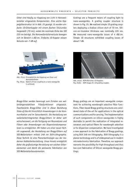
Abb. 25(a): Prinzipbild für die Kopplung von Faser und<br />
Nanowellenleiter.<br />
Fig. 25(a): Sketch of how coupling to a nano-waveguide<br />
is achieved.<br />
Bragg-Gitter werden bevorzugt zum Erzielen von wellenlängenselektiven<br />
Filterfunktionen eingesetzt.<br />
Faserbasierte Bragg-Gitter sind in dieser Beziehung<br />
State-of-the-Art hinsichtlich Anwendungen in der Kommunikation<br />
und im Sensorbereich. Die Herstellung von<br />
wellenleiterintegrierten Bragg-Gittern ist daher sehr<br />
wünschenswert, um die Fertigung von Resonatoren und<br />
Filtern oder Anwendungen wie Dispersionskompensatoren<br />
zu ermöglichen. Wir haben uns einer neuen Technik<br />
zugew<strong>and</strong>t, der Herstellung von Bragg-Gittern auf<br />
SOI-Wellenleitern mittels 248 nm DUV-Lithographie.<br />
Diese Technik ist eine Planartechnologie aus der modernen<br />
Halbleiterherstellung. Unser Ansatz ermöglicht<br />
daher die großvolumige Herstellung von solchen Gitterelementen<br />
und damit die preiswerte Fabrikation von<br />
SOI-Wellenleiterbauelementen.<br />
Gratings are a frequent means of coupling light to<br />
nano-waveguides. A grating coupler structure is<br />
shown in Fig. 25. We realized simple 1D grating couplers<br />
deploying a shallow silicon etch of 70 nm. Silicon-on-insulator<br />
thickness was nominally 220 nm.<br />
We measured nano-waveguide losses of 4 dB/cm.<br />
Simple 1D structures exhibited coupling losses of<br />
about 7 dB.<br />
Abb. 25(b): REM-Bild eines 1D-Kopplers.<br />
Fig. 25(b): SeM image of a 1D grating coupler.<br />
Bragg gratings are an important waveguide component<br />
for achieving wavelength selective filter functions.<br />
Fiber-based Bragg grating structures are considered<br />
state-of-the-art for applications in the optical<br />
communications <strong>and</strong> for sensing. the implementation<br />
of such components on silicon waveguides is highly<br />
desirable to permit the realization of integrated resonators<br />
<strong>and</strong> optical filters for wavelength selection<br />
or for dispersion compensation. We have investigated<br />
a new approach to the fabrication of Bragg gratings,<br />
using DuV 248 nm lithography. DuV lithography is a<br />
planar technology <strong>and</strong> is of widespread use in modern<br />
microelectronics fabrication. therefore, our approach<br />
warrants the possibility for high throughput <strong>and</strong> thus<br />
low-cost fabrication of Silicon waveguide Bragg gratings.


