

Deliverables and Services - IHP Microelectronics
Deliverables and Services - IHP Microelectronics
Deliverables and Services - IHP Microelectronics

Create successful ePaper yourself
Turn your PDF publications into a flip-book with our unique Google optimized e-Paper software.
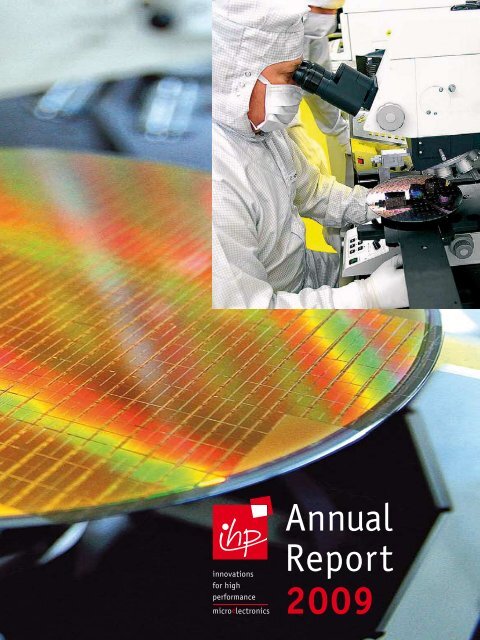
Annual<br />
Report<br />
2009<br />
A n n u A l R e p o R t 2 0 0 9
prof. Dr. Wolfgang Mehr<br />
Als Leibniz-Institut arbeitet das <strong>IHP</strong> vorrangig an langfristigen,<br />
strategischen Forschungsaufgaben. Dabei<br />
verbindet es Grundlagen- mit angew<strong>and</strong>ter Forschung.<br />
Das Institut entwickelt siliziumbasierte Systeme,<br />
Höchstfrequenz-Schaltungen und -Technologien für die<br />
drahtlose und Breitb<strong>and</strong>-Kommunikation und verifiziert<br />
diese durch Prototypen.<br />
Seine Kernkompetenzen sind:<br />
• Design von Systemen für die drahtlose Kommunikation,<br />
• Design analoger Hochfrequenzschaltungen,<br />
• Prozesstechnologie und<br />
• technologieorientierte Materialforschung.<br />
Das <strong>IHP</strong> verfügt als Besonderheit über eine vollständige<br />
0,13 µm BiCMOS-Pilotlinie für 200 mm Waferdurchmesser.<br />
Mit dieser werden sowohl innovative technologische<br />
Entwicklungen durchgeführt als auch sehr leistungsfähige<br />
BiCMOS-Technologien für Projekte des Instituts und<br />
Dritter angeboten. Die technologischen Entwicklungen<br />
zielen im Rahmen einer „More than Moore“ – Strategie<br />
auf die Realisierung zusätzlicher Funktionalitäten.<br />
Eine weitere wesentliche Besonderheit der Forschungsarbeit<br />
des <strong>IHP</strong> ist das vertikale Konzept mit der gezielten<br />
Nutzung von Synergien zwischen seinen Kernkompetenzen<br />
zur Erarbeitung vertikal optimierter Lösungen.<br />
Externe Kooperationen und die Verwertung von Arbeitsergebnissen<br />
erfolgen auf allen Ebenen – vom Material<br />
bis zu Systemen.<br />
2 A n n u A l R e p o R t 2 0 0 9<br />
V o r w o r t – F o r e w o r d<br />
As a leibniz-Institute, IHp works primarily on topics<br />
of longterm, strategic research. It combines basic <strong>and</strong><br />
applied research. the institute develops silicon-based<br />
systems, high-frequency circuits as well as process technologies<br />
for wireless <strong>and</strong> broadb<strong>and</strong> communications.<br />
typically the research results are verified by prototypes.<br />
the core competencies are:<br />
• Design of systems for wireless communication,<br />
• Design of analog high-frequency circuits,<br />
• process technology <strong>and</strong><br />
• technology-orientated materials research.<br />
As a distinctive feature, the IHp operates a full 0.13 µm<br />
BiCMoS pilot line for 200 mm wafer diameter. Based on<br />
this feature, both innovative technological developments<br />
<strong>and</strong> high-capacity BiCMoS technologies for projects<br />
of the institute are carried out <strong>and</strong> also offered to<br />
others. Following the “More than Moore” – strategy, the<br />
technological developments are aimed at the realization<br />
of additional functionalities.<br />
Another significant feature of the research work of the<br />
IHp is the vertical approach using synergies between its<br />
core competencies to develop vertically optimized solutions.<br />
external collaborations <strong>and</strong> the utilization of work<br />
results take place at all levels – from materials to systems.
Die Forschungsarbeiten des <strong>IHP</strong> ermöglichen innovative<br />
Lösungen für verschiedene Anwendungsbereiche.<br />
Beispiele dafür sind neben der drahtlosen und Breitb<strong>and</strong>-Kommunikation<br />
die Luft- und Raumfahrt, die<br />
Biotechnologie und Medizin, die Automobilindustrie,<br />
die Industrieautomatisierung und die Photonik.<br />
Das <strong>IHP</strong> ist für die Industrie, Hochschulen und <strong>and</strong>ere<br />
Forschungseinrichtungen ein gefragter Projektpartner.<br />
Im Jahr 2009 konnten Drittmittel von mehr als 11 Mill.<br />
Euro eingeworben werden. In mehreren nationalen und<br />
europäischen Verbundprojekten ist das <strong>IHP</strong> koordinierend<br />
tätig. Durch diese erfolgreiche Einwerbung von<br />
Drittmitteln wuchs das <strong>IHP</strong> weiter auf 270 Mitarbeiter<br />
aus 20 Ländern.<br />
Neben den internationalen und bundesweiten Kooperationen<br />
legt das <strong>IHP</strong> auch großen Wert auf die Zusammenarbeit<br />
mit Firmen und Hochschulen in Br<strong>and</strong>enburg<br />
und Berlin. So arbeitet das Institut an zahlreichen Projekten,<br />
bei denen die regionale Kooperation mit Firmen<br />
im Mittelpunkt steht. Mit mehreren Hochschulen betreibt<br />
es „Gemeinsame Labore“ zu ausgewählten Themen<br />
als eine besondere Form der Kooperation.<br />
Dieser Jahresbericht soll Ihnen einen Überblick zu den<br />
Forschungsprogrammen des Institutes und deren Zielen<br />
geben. Zu ausgewählten Forschungsprojekten finden Sie<br />
interessante Ergebnisse des Jahres 2009. Damit wollen<br />
wir Sie nicht nur informieren, sondern auch Ihr Interesse<br />
an einer Zusammenarbeit mit dem <strong>IHP</strong> wecken.<br />
An dieser Stelle möchten wir uns ganz herzlich bei allen<br />
bedanken, die unsere Erfolge möglich gemacht haben.<br />
Von der Br<strong>and</strong>enburgischen L<strong>and</strong>esregierung und von der<br />
Bundesregierung erhielten wir eine sehr starke Unterstützung,<br />
womit die Voraussetzungen für unsere Arbeit<br />
geschaffen werden konnten. Auf dieser Basis wurden die<br />
Forschungsergebnisse mit den Ideen und dem Fleiß unserer<br />
Mitarbeiterinnen und Mitarbeiter erarbeitet.<br />
Wolfgang Mehr Manfred Stöcker<br />
Wiss.-Techn. Geschäftsführer Adm. Geschäftsführer<br />
V o r w o r t – F o r e w o r d<br />
the research of IHp provides innovative solutions for various<br />
application areas. Apart from wireless <strong>and</strong> broadb<strong>and</strong><br />
communications, examples include aerospace,<br />
biotechnology <strong>and</strong> medicine, the automotive industry,<br />
industrial automation <strong>and</strong> photonics.<br />
For industry, universities <strong>and</strong> other research institutions<br />
the IHp is a sought-after project partner. In 2009 external<br />
funding amounted to more than 11 million euros.<br />
In several national <strong>and</strong> european projects the IHp works<br />
as a coordinator. Based on the successful fund raising<br />
IHp continued to grow to 270 staff members from 20<br />
countries.<br />
In addition to international <strong>and</strong> nationwide cooperation<br />
the IHp emphazises cooperation with companies<br />
<strong>and</strong> universities from Br<strong>and</strong>enburg <strong>and</strong> Berlin. e. g. the<br />
institute is working on numerous projects where the regional<br />
cooperation with companies is a core element. As<br />
a particular form of cooperation it operates “Joint labs”<br />
with several universities on selected topics.<br />
this annual report will give you an overview of the<br />
institute´s research programs <strong>and</strong> its objectives. For selected<br />
research projects you will find interesting results<br />
from 2009. Hereby, we not only want to inform you, but<br />
in addition would like to encourage you to cooperate<br />
with the IHp.<br />
At this point we would like to thank everyone who made<br />
our success possible. We received very strong support<br />
from the Federal State Government of Br<strong>and</strong>enburg <strong>and</strong><br />
the Federal Government of Germany laying the foundations<br />
for our work. Based on this, with their ideas <strong>and</strong><br />
efforts, our staff members achieved the research results<br />
presented here.<br />
A n n u A l R e p o R t 2 0 0 9
A n n u A l R e p o R t 2 0 0 9<br />
I N H A L t S V e r Z e I C H N I S – C o N t e N t S<br />
Contents
I N H A L t S V e r Z e I C H N I S – C o N t e N t S<br />
Vorwort<br />
Aufsichtsrat<br />
Wissenschaftlicher Beirat<br />
Forschung des <strong>IHP</strong><br />
Das Jahr 2009<br />
Ausgewählte Projekte<br />
Gemeinsame Labore<br />
Zusammenarbeit und Partner<br />
Gastwissenschaftler und Seminare<br />
Publikationen<br />
Angebote und Leistungen<br />
Wegbeschreibung zum <strong>IHP</strong><br />
2<br />
6<br />
7<br />
8<br />
28<br />
6<br />
70<br />
7<br />
78<br />
2<br />
2<br />
Foreword<br />
Supervisory Board<br />
Scientific Advisory Board<br />
IHp‘s Research<br />
update 2009<br />
Selected projects<br />
Joint labs<br />
Collaboration <strong>and</strong> partners<br />
Guest Scientists <strong>and</strong> Seminars<br />
publications<br />
<strong>Deliverables</strong> <strong>and</strong> <strong>Services</strong><br />
Directions to IHp<br />
A n n u A l R e p o R t 2 0 0 9
Aufsichtsrat<br />
Konstanze Pistor<br />
Vorsitzende<br />
Ministerium für Wissenschaft, Forschung und Kultur<br />
L<strong>and</strong> Br<strong>and</strong>enburg<br />
RD Dr. Volkmar Dietz<br />
Stellvertretender Vorsitzender<br />
Bundesministerium für Bildung und Forschung<br />
Dr.-Ing. Peter Draheim<br />
Philips GmbH, Hamburg<br />
Dr. Gunter Fischer<br />
<strong>IHP</strong> GmbH<br />
Prof. em. Dr. Helmut Gabriel<br />
Institut für Theoretische Physik<br />
Freie Universität Berlin<br />
Dr. Christoph Kutter<br />
Infineon Technologies AG<br />
Neubiberg<br />
Dr. Harald Richter<br />
<strong>IHP</strong> GmbH<br />
Prof. Dr. Ernst Sigmund<br />
Br<strong>and</strong>enburgische Technische Universität Cottbus<br />
MinR Gerhard Wittmer<br />
Ministerium der Finanzen<br />
L<strong>and</strong> Br<strong>and</strong>enburg<br />
6 A n n u A l R e p o R t 2 0 0 9<br />
A u F S I C H t S r A t – S u p e r V I S o r y B o A r d<br />
Supervisory Board<br />
Konstanze pistor<br />
Chair<br />
Ministry of Science, Research <strong>and</strong> Culture<br />
State of Br<strong>and</strong>enburg<br />
rd dr. Volkmar dietz<br />
Deputy Chair<br />
Federal Ministry of education <strong>and</strong> Research<br />
dr.-Ing. peter draheim<br />
philips GmbH, Hamburg<br />
dr. Gunter Fischer<br />
IHp GmbH<br />
prof. Helmut Gabriel<br />
Institute for theoretical physics<br />
Freie universität Berlin<br />
dr. Christoph Kutter<br />
Infineon technologies AG<br />
neubiberg<br />
dr. Harald richter<br />
IHp GmbH<br />
prof. ernst Sigmund<br />
Br<strong>and</strong>enburg university of technology, Cottbus<br />
Minr Gerhard wittmer<br />
Ministry of Finance<br />
State of Br<strong>and</strong>enburg
8 A n n u A l R e p o R t 2 0 0 9<br />
F o r S C H u N G d e S I H p – I H p ‘ S r e S e A r C H<br />
<strong>IHP</strong>‘s Research
Das <strong>IHP</strong> konzentriert sich auf die Erforschung und Entwicklung<br />
von Si-basierten Systemen, Höchstfrequenz-<br />
Schaltungen und -Technologien für die drahtlose und<br />
Breitb<strong>and</strong>kommunikation.<br />
Dabei arbeitet das Institut an den folgenden vier eng<br />
mitein<strong>and</strong>er verbundenen Forschungsprogrammen:<br />
1. Drahtlose Systeme und Anwendungen,<br />
2. Hochfrequenz-Schaltkreise,<br />
3. Technologieplattform für drahtlose und Breitb<strong>and</strong>kommunikation,<br />
4. Materialien für die Mikro- und Nanoelektronik.<br />
Die Forschungsprogramme nutzen die besonderen Möglichkeiten<br />
des <strong>IHP</strong>. So verfügt das Institut über eine Pilotlinie<br />
für technologische Forschungen und Entwicklungen<br />
sowie für die Fertigung von Prototypen und Kleinserien.<br />
Eine weitere Besonderheit ist das vertikale Forschungskonzept<br />
unter Nutzung der zusammenhängenden und<br />
aufein<strong>and</strong>er abgestimmten Kompetenzen des Institutes<br />
auf den Gebieten Systementwicklung, Schaltungsentwurf,<br />
Technologie und Materialforschung.<br />
Die Forschung des <strong>IHP</strong> setzt auf die typischen Stärken<br />
eines Leibniz-Instituts: Sie ist charakterisiert durch eine<br />
langfristige, komplexe Arbeit, die Grundlagenforschung<br />
mit anwendungsorientierter Forschung verbindet.<br />
Die Realisierung der Forschungsprogramme erfolgt mit<br />
Hilfe eines regelmäßig aktualisierten Portfolios von Projekten<br />
auf Basis einer mittelfristigen Roadmap. Die Aktualisierung<br />
geschieht aufgrund inhaltlicher Erfordernisse<br />
sowie der Möglichkeiten für Kooperationen und<br />
Finanzierung. Drittmittelprojekte werden im Einklang<br />
mit den strategischen Zielen des <strong>IHP</strong> eingeworben.<br />
F o r S C H u N G d e S I H p – I H p ‘ S r e S e A r C H<br />
IHp is focused on the research <strong>and</strong> development of<br />
silicon-based systems, high-frequency circuits <strong>and</strong><br />
technologies for wireless <strong>and</strong> broadb<strong>and</strong> communication.<br />
the institute is working on the following four closely<br />
connected research programs:<br />
1. Wireless Systems <strong>and</strong> Applications,<br />
2. RF Circuits,<br />
3. technology platform for Wireless <strong>and</strong> Broadb<strong>and</strong><br />
Communication,<br />
4. Materials for Micro- <strong>and</strong> nanoelectronics.<br />
the research programs make use of the special opportunities<br />
provided by the IHp. For instance, the<br />
institute has a pilot line for technological research<br />
<strong>and</strong> developments as well as for manufacturing prototypes<br />
<strong>and</strong> small series. An additional feature is the<br />
vertical research concept employing the associated<br />
<strong>and</strong> harmonized competencies of the institute in the<br />
fields of system development, circuit design, technology<br />
<strong>and</strong> materials research.<br />
the research of the IHp is based on the typical<br />
strengths of a leibniz Institute: it is dominated by<br />
long-term, complex efforts which connect basic research<br />
with application-oriented research.<br />
the realization of the research programs is accomplished<br />
utilizing a project portfolio based on a<br />
medium-term roadmap. the project portfolio is regularly<br />
updated according to content requirements as<br />
well as through opportunities for cooperations <strong>and</strong><br />
outside funding. Grant projects are acquired in accordance<br />
with the strategic goals of IHp.<br />
A n n u A l R e p o R t 2 0 0 9<br />
9
Die Forschungsprogramme haben die folgenden<br />
wesentlichen Ziele:<br />
Drahtlose Systeme und Anwendungen<br />
In diesem Programm werden komplexe Systeme für<br />
die drahtlose Kommunikation in Form von Prototypen<br />
und Anwendungen untersucht und entwickelt. Ziel<br />
sind Hardware/Software-Systemlösungen auf hochintegrierten<br />
Single-Chips. Der vertikale Forschungsansatz<br />
zeigt sich auch in der Architektur der erarbeiteten<br />
Systeme. Im Wesentlichen wird die Wechselwirkung<br />
zwischen verschiedenen Schichten optimiert und eine<br />
vertikale Migration semantischer Elemente realisiert.<br />
Die drei Hauptforschungsrichtungen sind WLANs hoher<br />
Performance, Sensornetzwerke mit extrem geringem<br />
Energieverbrauch und Design for Testability.<br />
Für WLANs hoher Performance sollen Datenraten bis<br />
10 Gbps bei Trägerfrequenzen bis zu 60 GHz erreicht<br />
werden. Weiterführende Arbeiten hin zu Datenraten bis<br />
100 Gbps und Trägerfrequenzen bis 300 GHz werden im<br />
Grundlagenbereich dieses Forschungsprogramms vorbereitet.<br />
Ein weiteres wichtiges Forschungsthema ist die<br />
Quality of Service im Hochlastbereich, da bei zunehmender<br />
Nutzung drahtloser Technologien Zugriffskonflikte<br />
nicht zu vermeiden sind.<br />
Die Forschung zu Systemen mit geringem Energieverbrauch<br />
hat zum Ziel, Sensornetze auf Basis hochintegrierter<br />
Chips zu realisieren. Typische Anwendungen<br />
dafür sind Body-Area-Netze für medizinische Anwendungen<br />
oder im Wellness-Bereich. In diesem Zusammenhang<br />
werden neue Netzarchitekturen, verteilte,<br />
ressourcenarme Middlewareansätze, neue energieeffiziente<br />
Medienzugriffsprotokolle sowie energieeffiziente<br />
Transceiver erforscht und realisiert. UWB-Technologien<br />
sind Beispiele für Kommunikation im Nahbereich und<br />
Anwendungen mit hohen Ortsauflösungseigenschaften.<br />
Andere Funklösungen im Bereich Sensornetze sind PSSS<br />
(Parallel Sequence Spread Spectrum) - basierte Ansätze,<br />
die sich durch besonders hohe B<strong>and</strong>breiteneffizienz<br />
auszeichnen.<br />
0 A n n u A l R e p o R t 2 0 0 9<br />
F o r S C H u N G d e S I H p – I H p ‘ S r e S e A r C H<br />
Significant goals of IHp’s research programs are<br />
specified below.<br />
wireless Systems <strong>and</strong> Applications<br />
this program investigates <strong>and</strong> develops complex systems<br />
for wireless communications as prototypes <strong>and</strong><br />
applications with the objective of finding solutions<br />
for hardware / software systems on highly integrated<br />
single chips. the vertical research approach is also reflected<br />
in the architecture of the addressed systems.<br />
Basically, inter-layer interaction is optimized <strong>and</strong> a<br />
vertical migration of semantic elements is performed.<br />
the three major directions of research are high performance<br />
WlAn, ultra-low power sensor networks <strong>and</strong><br />
design for testability.<br />
the target of high performance WlAn research is to<br />
achieve a data rate up to 10 Gbps at carrier frequencies<br />
of up to 60 GHz. Continuing activities towards data<br />
rates up to 100 Gbps <strong>and</strong> carrier frequencies up to<br />
300 GHz will be carried out in the basic research area<br />
of this research program. Quality of Service in the high<br />
load region is an additional important research field,<br />
because the increasing use of wireless technologies<br />
will inevitably result in growing conflicts of access.<br />
the research on systems with low energy consumption<br />
is directed towards sensor networks on single<br />
chips. typical applications are body-area networks<br />
for health care or wellness. In this context new network<br />
architectures, distributed low resource middleware<br />
concepts, new energy efficient protocols for medium<br />
access as well as energy efficient transceivers<br />
are investigated <strong>and</strong> realized. uWB technologies are<br />
examples for short-range communication as well as<br />
applications requiring high spatial resolution. other<br />
radio-based solutions for sensor networks are pSSS<br />
(parallel Sequence Spread Spectrum) – based approaches,<br />
distinguished by exceptionally high b<strong>and</strong>width<br />
efficiency.
Die Forschung zu kontextabhängigen Middleware-Systemen<br />
betrifft insbesondere auch die Erhaltung der Privatsphäre<br />
und die Sicherheit bei der Nutzung mobiler<br />
Endgeräte. Darüber hinaus wird die symmetrische bzw.<br />
asymmetrische Verteilung von Ressourcen zwischen<br />
Endgeräten und Servern im Gesamtsystem untersucht.<br />
Hochfrequenz-Schaltkreise<br />
In diesem Programm werden integrierte mm-Wellen-<br />
Schaltkreise & Synthesizer, Breitb<strong>and</strong>-Mischsignal-<br />
Schaltkreise, sowie Schaltkreise für drahtlose Anwendungen<br />
mit sehr geringem Energieverbrauch entwickelt<br />
und als Prototypen realisiert.<br />
Integrierte Millimeterwellen-HF-Schaltkreise für Front-<br />
ends und Synthesizer zum Einsatz in der drahtlosen<br />
Kommunikation bei Frequenzen von etwa 10 bis<br />
> 200 GHz werden derzeit entwickelt.<br />
Für die glasfasergestützte Breitb<strong>and</strong>kommunikation<br />
werden Konzepte und elektronische Komponenten für<br />
Glasfasersysteme mit Datenraten bis über 100 Gbps<br />
pro Laser-Wellenlänge entwickelt. Beispiele dafür sind<br />
extrem breitb<strong>and</strong>ige Verstärker, A/D- und D/A-W<strong>and</strong>ler,<br />
schnelle Logik sowie gemischt analog/digitale Signalverarbeitung<br />
in Echtzeit.<br />
Extrem energiesparende HF-Frontends und Komponenten<br />
werden für Sensornetze entwickelt, mit denen die<br />
geforderte Batterie-Lebensdauer von 10 Jahren erreichbar<br />
ist. Beispielhafte Entwicklungen sind hier energieeffiziente<br />
UWB Transceiver-Schaltkreise mit impulsbasierter<br />
Modulation und Wake-Up Radios mit extrem<br />
niedriger Stromaufnahme.<br />
F o r S C H u N G d e S I H p – I H p ‘ S r e S e A r C H<br />
Research in context-sensitive middleware systems<br />
especially addresses privacy <strong>and</strong> security matters in<br />
using mobile devices. Moreover, the symmetrical <strong>and</strong><br />
asymmetrical resource distribution between client<br />
<strong>and</strong> server parts of the overall system is investigated.<br />
rF Circuits<br />
In this program mm-wave circuits, broadb<strong>and</strong> mixedsignal<br />
ICs <strong>and</strong> ICs for ultra-low-power wireless applications<br />
will be designed <strong>and</strong> realized as prototypes.<br />
Millimeter-Wave RF ICs for frontends <strong>and</strong> synthesizers<br />
for wireless communication at currently 10 to<br />
> 200 GHz are under development.<br />
Concepts <strong>and</strong> electronic components for fiber-optic<br />
broadb<strong>and</strong> communication systems with data rates<br />
up to > 100 Gbps per laser wavelength will be developed.<br />
examples are extremely broadb<strong>and</strong> amplifiers,<br />
A/D- <strong>and</strong> D/A-converters as well as fast logic <strong>and</strong><br />
real-time analog/digital signal processing.<br />
ultra-low-power RF frontends <strong>and</strong> components for<br />
sensor networks with a target battery lifetime of ten<br />
years are under development. examples of developments<br />
are energy-efficient uWB transceiver circuits<br />
with impulse-based modulation <strong>and</strong> wake-up radios<br />
with extremly low power consumption.<br />
A n n u A l R e p o R t 2 0 0 9
Technologieplattform für drahtlose und Breitb<strong>and</strong>kommunikation<br />
In diesem Programm werden Technologien (insbesondere<br />
BiCMOS-Technologien) mit zusätzlichen Funktionen<br />
durch die modulare Erweiterung industrieller CMOS-<br />
Technologien entwickelt. Die Schwerpunkte in diesem<br />
Programm sind Technologien mit hoher Performance,<br />
kostengünstige Technologien für System-on-Chip, sowie<br />
die Sicherung des Zugriffs interner und externer Designer<br />
auf die Technologien des <strong>IHP</strong>.<br />
Die Forschung in Richtung Technologien hoher Performance<br />
zielt auf extrem schnelle SiGe HBTs, einschließlich<br />
komplementärer Bauelemente und neuer Bauelementekonzepte<br />
für Anwendungen bei Frequenzen bis ><br />
100 GHz.<br />
Zielstellung der Forschung für kostengünstige Technologien<br />
ist es, BiCMOS-Technologien mit ausreichender<br />
Performance und geringen Fertigungskosten zu entwickeln<br />
sowie darin zusätzliche Module wie HF-LDMOS,<br />
Flash und passive Bauelemente zu integrieren.<br />
Die 0,25-µm- und 0,13-µm-BiCMOS-Technologien des<br />
<strong>IHP</strong> sind europa- und weltweit für Designer nutzbar.<br />
Ein Zeitplan für die entsprechenden technologischen<br />
Durchläufe in der Pilotlinie in Frankfurt (Oder) ist über<br />
die Internetadresse des <strong>IHP</strong> einsehbar.<br />
2 A n n u A l R e p o R t 2 0 0 9<br />
F o r S C H u N G d e S I H p – I H p ‘ S r e S e A r C H<br />
technology platform for wireless <strong>and</strong> Broadb<strong>and</strong><br />
Communication<br />
the goal of this program is to develop value-added<br />
technologies, preferably BiCMoS technologies, by<br />
the modular extension of industrial CMoS. the focal<br />
points in this program are technologies with high performance,<br />
low-cost technologies for system-on-chip,<br />
<strong>and</strong> the provision of technology access for internal<br />
<strong>and</strong> external designers.<br />
the research towards high-performance technologies<br />
targets ultrafast SiGe HBts, including complementary<br />
devices <strong>and</strong> new device concepts, for applications at<br />
frequencies of up to > 100 GHz.<br />
the aim of the research for low-cost technologies is<br />
to develop BiCMoS technologies with ample performance<br />
<strong>and</strong> low manufacturing costs <strong>and</strong> to integrate<br />
additional modules such as RF lDMoS, Flash <strong>and</strong> passive<br />
devices.<br />
IHp’s 0.25 µm <strong>and</strong> 0.13 µm BiCMoS technologies are<br />
available for designers in europe <strong>and</strong> throughout the<br />
world.<br />
A schedule for technological runs in the pilot line<br />
in Frankfurt (oder) can be found via IHp`s internet<br />
address.
Materialien für die Mikro- und Nanoelektronik<br />
Die Materialforschung am <strong>IHP</strong> hat die Integration<br />
neuer Materialien in gegenwärtige und zukünftige Si-<br />
Technologien zum Ziel, um so verbesserte, zusätzliche<br />
oder neuartige Funktionalitäten zu erreichen. Darüber<br />
hinaus werden Grundlagen für neue Forschungsgebiete<br />
am <strong>IHP</strong> geschaffen.<br />
Aktuelle Schwerpunkte der Arbeiten zu neuen Hochk-Dielektrika<br />
sind binäre und ternäre Legierungen für<br />
zukünftige Anwendungen in MIM-Kondensatoren, Speichern<br />
und Transistoren sowie als Epitaxievermittler<br />
für globale hochwertige heteroepitaktische Halbleiterschichten(Halbleiter-Isolator-Halbleiter-Schichtstapel).<br />
Weiterhin werden neue Materialien für akustische<br />
Oberflächenwellenfilter (SAW-Filter) und für nichtflüchtige<br />
Speicher (NVM-Speicher) bewertet.<br />
Zukünftige Aktivitäten konzentrieren sich auf integrierbare<br />
THz-Bauelemente, insbesondere den HBT,<br />
MIIMIM-Tunneltransistoren mit heißen Elektronen sowie<br />
Graphen-Transistoren.<br />
Gegenst<strong>and</strong> der Arbeiten im Gemeinsamen Labor mit<br />
der BTU Cottbus ist die Si-Materialforschung. Dabei sollen<br />
die Eigenschaften des Si-Materials maßgeschneidert<br />
werden, um neue Anwendungen zu ermöglichen und um<br />
bestehende Anwendungen zu verbessern.<br />
Schwerpunkte sind die grundlagenorientierte Vorlaufforschung<br />
zu Si-basierten Lichtemittern für die optische<br />
Datenübertragung, zum „Defect Engineering“<br />
für zukünftige Si-Wafer, zum B<strong>and</strong>strukturdesign und<br />
Ladungsträgertransport in Si-basierten Quantenstrukturen<br />
und zur Beherrschung der elektrischen Eigenschaften<br />
von Kristalldefekten in Solar-Si.<br />
F o r S C H u N G d e S I H p – I H p ‘ S r e S e A r C H<br />
Materials for Micro- <strong>and</strong> Nanoelectronics<br />
Materials research at IHp targets the integration of<br />
new materials into current <strong>and</strong> future silicon technologies<br />
to achieve additional, better or innovative<br />
functionalities. It also gears towards the preparation<br />
of new research fields at the institute.<br />
Current focal points of the activities with high-k dielectrics<br />
are binary <strong>and</strong> ternary alloys for future applications<br />
in MIM capacitors, memories <strong>and</strong> transistors<br />
as well as for epitaxy mediation for global high quality<br />
heteroepitaxial semiconductor layers (semiconductor-insulator-silicon<br />
stacks). Additionally, new<br />
materials for SAW filters <strong>and</strong> non-volatile memories<br />
are evaluated.<br />
Future activities will concentrate on tHz devices<br />
with the capability to be integrated, preferably HBts,<br />
MIIMIM hot electron tunnelling transistors <strong>and</strong> graphene<br />
transistors,<br />
Silicon materials research is the subject matter of the<br />
Joint lab IHp/Btu. Silicon properties are tailored<br />
to enable new applications <strong>and</strong> to improve existing<br />
ones.<br />
Focuses are initial basic research for Si-based light<br />
emitters for optical data transmission, defect engineering<br />
for future silicon wafers, b<strong>and</strong> structure design<br />
<strong>and</strong> charge carrier transport in Si-based quantum<br />
structures, <strong>and</strong> the control of electrical properties of<br />
crystal defects in solar silicon.<br />
A n n u A l R e p o R t 2 0 0 9
A n n u A l R e p o R t 2 0 0 9<br />
d A S J A H r 2 0 0 8 – u p d A t e 2 0 0 8<br />
Update 2009
Das Jahr 2009<br />
Die Forschungsergebnisse des Institutes sind 2009 in<br />
126 schriftlichen Publikationen und 180 Vorträgen<br />
veröffentlicht. Darüber hinaus wurden mehrere wissenschaftliche<br />
Veranstaltungen maßgeblich durch Mit-<br />
arbeiter des <strong>IHP</strong> organisiert. Dazu gehören die 13.<br />
„GADEST“ (Gettering <strong>and</strong> Defect Engineering in Semiconductor<br />
Technology), die 2009 in Döllnsee-Schorfheide<br />
stattf<strong>and</strong>, die „Wilhelm <strong>and</strong> Else Heraeus Physics<br />
School“ in Bad Honnef sowie der „8. Workshop High-<br />
Performance SiGe BiCMOS“ mit anschließendem zweitägigen<br />
Tutorial zu den <strong>IHP</strong> Design Kits in Frankfurt<br />
(Oder).<br />
Zum Ausbau der Kooperation mit regionalen Firmen<br />
gab es am <strong>IHP</strong> erstmals einen Br<strong>and</strong>enburger Sensornetztag<br />
mit Firmen dieser Branche. Studierenden relevanter<br />
Studienrichtungen bot die „8. Sommerschule<br />
Mikroelektronik“ Gelegenheit, die Arbeit am <strong>IHP</strong> kennen<br />
zu lernen. Ergänzt wurde diese Veranstaltung durch<br />
die gemeinsam mit dem Investorcenter Ostbr<strong>and</strong>enburg<br />
durchgeführte „Sommerschule Solar“, die ebenfalls von<br />
mehr als 20 Studenten besucht wurde. Darüber hinaus<br />
f<strong>and</strong>en mehrere Treffen großer Verbundprojekte am Institut<br />
statt.<br />
Am 16. März 2009 wurde Professor W. Mehr durch die<br />
Br<strong>and</strong>enburgische Wissenschaftsministerin und dem<br />
Wirtschaftsminister zum Wissenschaftsbotschafter für<br />
den Wirtschaftsst<strong>and</strong>ort Br<strong>and</strong>enburg ernannt.<br />
Den EEEfCOM-Innovationspreis für praxisrelevante Forschung<br />
erhielt Professor R. Kraemer zusammen mit<br />
Wissenschaftlern der TU Dresden und der Universität<br />
von Cantabria für das Projekt „MIMAX“.<br />
d A S J A H r 2 0 0 9 – u p d A t e 2 0 0 9<br />
update 2009<br />
In 2009 the research results of the institute were made<br />
public in 126 written publications <strong>and</strong> 180 oral presentations.<br />
In addition, several scientific events were<br />
primarily organized by members of the IHp staff.<br />
these include the 13 th “GADeSt (Gettering <strong>and</strong> Defect<br />
engineering in Semiconductor technology) which was<br />
held in 2009 in Döllnsee-Schorfheide, the “Wilhelm<br />
<strong>and</strong> else Heraeus physics School“ in Bad Honnef <strong>and</strong><br />
the “8 th Workshop High-performance SiGe BiCMoS”,<br />
followed by a two-day tutorial on the IHp Design Kits<br />
which took place in Frankfurt (oder).<br />
to extend cooperations with regional companies, IHp<br />
held the first “Br<strong>and</strong>enburg Sensornetztag” involving<br />
companies of this industry. the “8 th Summer School<br />
<strong>Microelectronics</strong>” offered students of relevant fields<br />
of study an opportunity to learn about the work at<br />
IHp. this event was complemented by the “Summer<br />
School Solar“ organized jointly with the Investorcenter<br />
ostbr<strong>and</strong>enburg. More than 20 students attended<br />
each of these. In addition several large meetings of<br />
major collaborative projects took place at the institute.<br />
on March 16 th 2009 professor W. Mehr was appointed<br />
science ambassador for the industrial location Br<strong>and</strong>enburg<br />
by the science minister <strong>and</strong> the minister of<br />
economic affairs of the Federal State of Br<strong>and</strong>enburg.<br />
the eeefCoM Innovation Award for practice-orientated<br />
research was awarded to professor R. Kraemer<br />
together with scientists from the tu Dresden <strong>and</strong> the<br />
university of Cantabria for the project “MIMAX“ .<br />
A n n u A l R e p o R t 2 0 0 9
Wissenschaftliche Ergebnisse<br />
Im Folgenden wird auf ausgewählte wissenschaftliche<br />
Fortschritte in den Forschungsprogrammen im Jahr<br />
2009 hingewiesen. Detaillierte Ergebnisse einzelner<br />
Forschungsprojekte sind im nachfolgenden Kapitel<br />
„Ausgewählte Projekte“ dargestellt.<br />
Drahtlose Systeme und Anwendungen<br />
Hauptziel des Projektes EASY-A (Enablers for Ambient<br />
<strong>Services</strong> <strong>and</strong> Systems – 60 GHz Broadb<strong>and</strong> Links) ist die<br />
Realisierung einer drahtlosen Datenübertragung mit<br />
einer Rate von etwa 10 Gbps. Das <strong>IHP</strong> ist Konsortialführer<br />
in diesem durch das BMBF geförderten Projekt<br />
mit einem Gesamtvolumen von 18 Mio. Euro. In diesem<br />
Projekt wurde ein Demonstrator mit einer Echtzeit Videoübertragung<br />
im 60-GHz-B<strong>and</strong> über eine Entfernung<br />
von mehreren Metern realisiert. Ein zweiter Demonstrator<br />
mit 60 GHz Trägerfrequenz überträgt UWB-Signale.<br />
Hier konnte durch Optimierung der Anpassungen und<br />
der Sendeleistungen eine Reichweite von über 40 m<br />
gezeigt werden. Mit den Arbeiten im Bereich 60-GHz-<br />
Kommunikation ist das <strong>IHP</strong> in zwei umfangreichen<br />
Buchbeiträgen vertreten. Die 60-GHz-Hardware wurde<br />
erfolgreich an mehrere Unternehmen zu Testzwecken<br />
verkauft.<br />
Erste Ergebnisse der EU-Projekte GALAXY, MIMAX und<br />
OMEGA wurden auf mehreren internationalen Konferenzen<br />
vorgestellt.<br />
Im Rahmen des von <strong>IHP</strong> koordinierten Projektes GALA-<br />
XY (GALs interfAce for compleX digital sYstem integration)<br />
wurden zwei Patente eingereicht. Das Erste zum<br />
effizienten und kostengünstigen Test von asynchronen<br />
Protokollen während der Laufzeit und das Zweite zu optimalen<br />
Interfaceschaltungen zwischen digitalen Blöcken.<br />
Für unsere Veröffentlichung über GALS-Konzepte<br />
wurde auf der ICCD (International Conference on Computer<br />
Design) 2009 der Best Paper Award verliehen.<br />
6 A n n u A l R e p o R t 2 0 0 9<br />
d A S J A H r 2 0 0 9 – u p d A t e 2 0 0 9<br />
Scientific results<br />
In the following, selected scientific advances in the<br />
research programs in 2009 will be pointed out. Detailed<br />
results of single research projects will be described<br />
in the next chapter “Selected projects”.<br />
wireless Systems <strong>and</strong> Applications<br />
the primary objective of the project eASY-A (enablers<br />
for Ambient <strong>Services</strong> <strong>and</strong> Systems – 60 GHz Broadb<strong>and</strong><br />
links) is to realize wireless communication with<br />
a data rate of approximately 10 Gbps. the IHp is the<br />
leader of this project, which is funded by the Federal<br />
Ministry of education <strong>and</strong> Research <strong>and</strong> has a total<br />
volume of 18 million euro. We were able to demonstrate<br />
a real-time video transmission in the 60 GHz<br />
b<strong>and</strong> over a distance of several meters. A second demonstrator<br />
with a carrier frequency of 60 GHz transmits<br />
uWB signals. A transmission range of more than<br />
40 m was reached after optimization of the matching<br />
<strong>and</strong> power. IHp`s work on 60 GHz communication is<br />
described in two extensive book chapters. the 60 GHz<br />
hardware was sold to several companies for test purposes.<br />
First results of the eu projects GAlAXY, MIMAX <strong>and</strong><br />
oMeGA were presented at numerous international<br />
conferences.<br />
the project GAlAXY (GAls interfAce for compleX digital<br />
sYstem integration) is coordinated by the IHp. two<br />
patents were filed within this project. the first one is<br />
for efficient <strong>and</strong> economic test of asynchronous protocols<br />
during runtime, <strong>and</strong> the second one is about<br />
optimal interface circuitries between digital blocks.<br />
For our publication on GAlS concepts we received<br />
the Best paper Award at the ICCD (International Conference<br />
on Computer Design) 2009.
Im Projekt MIMAX (Advanced MIMO systems for MAXimum<br />
reliability <strong>and</strong> performance) wurde ein Patent für<br />
das optimale Training der Amplituden und Phasenwerte<br />
für MIMO-Parameter eingereicht.<br />
Im Rahmen des Projektes OMEGA (Home Gigabit Access)<br />
wurde ein Verfahren für die semantische Beschreibung<br />
von Quality-of-Service-Parametern zwischen verschiedenen<br />
MAC-Protokollen entwickelt. Das darauf aufbauende<br />
Framework zur Realisierung der Control-Plane<br />
wurde entwickelt und dient nun den Entwicklern in den<br />
Partnerorganisationen zur Umsetzung der Control-Plane<br />
Steuerungs-Algorithmen.<br />
Das vom BMWi geförderte Projekt HOMEPLANE (Home<br />
Media Plattform und Netzwerke) wurde am 5. Mai 2009<br />
mit einem Anwenderworkshop erfolgreich abgeschlossen.<br />
Es wurden Ergänzungen der Hard- und Firmware<br />
im WLAN-Chipset des <strong>IHP</strong> nach dem St<strong>and</strong>ard IEEE<br />
802.11a / g entwickelt und implementiert. Diese bildeten<br />
die Voraussetzungen für innovative Algorithmen<br />
der TU Dortmund, welche die Medienströme verwalten<br />
und die benötigte Dienstgüte garantieren. Das <strong>IHP</strong> hat<br />
außerdem neue Komponenten zur Sicherheit der Middleware<br />
entwickelt. Die Projektpartner haben dies mit<br />
dem Ressourcenmanagement, der Netzorganisation und<br />
den Benutzerschnittstellen zu einem aussagekräftigen<br />
Demonstrator integriert. Der Homeplane-Demonstrator<br />
wurde dazu in einem Musterhaus installiert und dem<br />
BMWi und <strong>and</strong>eren Interessenten vorgeführt. Aufbauend<br />
auf den Arbeiten in Homeplane wird nun an der<br />
Weiterentwicklung der WLAN Komponenten in Richtung<br />
Car-2-x Systeme gearbeitet.<br />
Ein Ziel des Institutes als registrierter Partner der ESA<br />
ist es, den im <strong>IHP</strong> entwickelten Prozessor LEON-3-FT in<br />
eine große Mission der ESA einzubringen. Zusätzlich<br />
werden derzeit Projekte für eine generalisierte Prozessorbasis<br />
für Satelliten zusammen mit der DLR vorangetrieben.<br />
Ein neuer Speichergenerator für PROMs wurde<br />
zusammen mit der ukrainischen Firma Genesys realisiert<br />
und getestet.<br />
d A S J A H r 2 0 0 9 – u p d A t e 2 0 0 9<br />
In the project MIMAX (Advanced MIMo systems for<br />
MAXimum reliability <strong>and</strong> performance) a patent was<br />
filed for the optimal training of amplitudes <strong>and</strong><br />
phases for MIMo-parameters.<br />
A method for the semantic description of Quality-of-<br />
Service-parameters between different MAC protocols<br />
was developed in the project oMeGA (Home Gigabit<br />
Access). A framework for the realization of the control<br />
plane which builds on this was developed <strong>and</strong> is<br />
used now by the developers in the partner organisations<br />
for the realization of the control algorithm in<br />
this plane.<br />
the project HoMeplAne (Home Media platform <strong>and</strong><br />
networks), financed by the Federal Ministry of economics<br />
<strong>and</strong> Research, was successfully finished with<br />
a user workshop on May 5 th 2009. Supplements of the<br />
hard- <strong>and</strong> firmware in IHp`s WlAn chipset for the<br />
Ieee 802.11a/g st<strong>and</strong>ard were developed <strong>and</strong> implemented.<br />
they are the preconditions for innovative<br />
algorithms of the tu Dortmund which manage the<br />
media streams <strong>and</strong> guarantee the required quality of<br />
service. In addition, the IHp has developed new components<br />
for middleware security. the project partners<br />
have integrated this with resource management, network<br />
organisation <strong>and</strong> user interface to a compelling<br />
demonstrator. the HoMeplAne demonstrator was<br />
installed in a show house <strong>and</strong> demonstrated to the<br />
BMWi (Federal Ministry of economics <strong>and</strong> technology)<br />
<strong>and</strong> additional interested groups. Based on the<br />
HoMeplAne works WlAn components are now further<br />
developed towards car-2-x systems.<br />
It is an aim of the institute as a registered partner<br />
of the eSA to introduce IHp`s leon-3-Ft processor<br />
into a great eSA mission. In addition, several projects<br />
for a general processor basis for satellites are being<br />
prepared in cooperation with the DlR. A new memory<br />
generator for pRoMs was designed <strong>and</strong> tested in cooperation<br />
with the ukrainian company Genesys.<br />
A n n u A l R e p o R t 2 0 0 9<br />
7
Ein erster sicherer Knoten für drahtlose Sensornetze<br />
wurde für das Bundesamt für Sicherheit in der Informationstechnik<br />
(BSI) entwickelt. Dieser Knoten soll<br />
Sensornetze im Grenzüberwachungsbereich gegen Manipulationen<br />
und das Eindringen von Außen schützen.<br />
Für diesen Knoten wurden eine Hardware- sowie eine<br />
Softwarearchitektur entworfen. Die Hardwarearchitektur<br />
wurde umgesetzt und in die Präparation eingesteuert.<br />
Zusätzlich wurde das Design erfolgreich auf einem<br />
FPGA umgesetzt und erste Teile der Software wurden<br />
auf dieser Plattform bereits fertig gestellt.<br />
Für die Kommunikation von Sensorknoten wird der<br />
St<strong>and</strong>ard IEEE 802.15.4 realisiert. Ein erstes Design der<br />
analogen und digitalen Komponenten des 868-MHz-<br />
Frontends wurde fertig gestellt und in die Fertigung<br />
eingesteuert. Ein Parallel Sequence Spread Spectrum<br />
(PSSS)-basiertes Basisb<strong>and</strong> für die Sensornetzkommunikation<br />
wurde realisiert. Für den neuen Metering-<br />
St<strong>and</strong>ard nach EN15787-4 wurde das digitale Baseb<strong>and</strong><br />
realisiert und eine zusätzliche Version mit erhöhter<br />
Zuverlässigkeit umgesetzt. Die Implementierung des<br />
802.15.4 Medienzugriffsprotokolls wurde für Reduced-<br />
Function- und Full-Function-Devices abgeschlossen.<br />
2009 wurden die Projekte MATRIX (Middleware für die<br />
Realisierung Internetbasierter telemedizinischer Dienste,<br />
gefördert durch das BMBF), SMART (Secure, Mobile<br />
visual sensor networks ARchiTecture, ein ARTEMIS-Projekt)<br />
sowie WSAN4CIP (Wireless Sensor <strong>and</strong> Actuator<br />
Networks for critical infrastructures, gefördert durch<br />
die EU) neu gestartet. Das <strong>IHP</strong> ist der technische Koordinator<br />
des Projektes WSAN4CIP, das im gemeinsamen<br />
ICT und Security Call der EU beantragt und als bestes<br />
Proposal ausgewählt wurde. In diesem Projekt wurde<br />
das erste Meilenstein-Dokument mit der Auswahl der<br />
Demonstrator-Szenarien und von Protokoll-Ansätzen<br />
bereits fertig gestellt.<br />
Im durch das BMBF geförderten Projekt FeuerWhere<br />
(Tracking Fire Fighters) wurde ein Demonstrator für das<br />
Body Area Netz realisiert. Dieses dient zur Überwachung<br />
von Parametern am Körper des Feuerwehrmannes bzw.<br />
am Feuerschutzanzug. Der Demonstrator unterstützt<br />
drei unterschiedliche Funkverfahren und kann flexibel<br />
konfiguriert werden.<br />
8 A n n u A l R e p o R t 2 0 0 9<br />
d A S J A H r 2 0 0 9 – u p d A t e 2 0 0 9<br />
In the area of wireless sensor networks a first secure<br />
node was developed for the Federal office for<br />
Information Security (BSI). this secure node should<br />
protect sensor networks in borderline applications<br />
against external manipulation <strong>and</strong> invasion. A hardware<br />
<strong>and</strong> software architecture was designed for this<br />
node. the hardware architecture was realized <strong>and</strong> is<br />
now in preparation. Additionally, the design was successfully<br />
realized as an FpGA, <strong>and</strong> first software parts<br />
for this platform are already running.<br />
the communication between sensor nodes will be realized<br />
with the st<strong>and</strong>ard Ieee 802.15.4. A first design<br />
for the analog <strong>and</strong> digital components of an 868 MHz<br />
front-end are under preparation in the pilot line. A<br />
parallel Sequence Spread Spectrum (pSSS) based base<br />
b<strong>and</strong> for the communication in the sensor network<br />
was realized. the digital baseb<strong>and</strong> <strong>and</strong> an additional<br />
highly reliable version were realized for the new metering<br />
st<strong>and</strong>ard en15787-4. the implementation of<br />
the 802.15.4 medium access protocol was finished for<br />
reduced-function as well as full-function devices.<br />
In 2009 the new projects MAtRIX (middleware for<br />
internet-based telemedicine services, funded by the<br />
BMBF), SMARt (Secure, Mobile visual sensor networks<br />
ARchitecture, an ARteMIS project) <strong>and</strong> WSAn4CIp<br />
(Wireless Sensor <strong>and</strong> Actuator networks for critical<br />
infrastructure, funded by the eu) were started. IHp<br />
is the technical coordinator of the project WSAn4CIp,<br />
which was applied for in the joint european ICt <strong>and</strong><br />
security call <strong>and</strong> selected as the best proposal. In this<br />
project, the first milestones with the selected demonstrator<br />
scenarios <strong>and</strong> approaches for the protocol<br />
were finished.<br />
In the BMBF supported project FeuerWhere (tracking<br />
Fire Fighters) a demonstrator for the body area network<br />
was realized. It monitors the body parameters of<br />
the fire fighter <strong>and</strong> the fire suit, respectively. the demonstrator<br />
supports three different radio st<strong>and</strong>ards<br />
<strong>and</strong> can be configured flexibly.
Zusätzlich konnten 2 ForMaT-Projekte (ForMaT: Forschung<br />
für den Markt im Team) aus dem Bereich Sensornetze<br />
eingeworben werden. ForMaT-Projekte können<br />
bei erfolgreichem Abschluss die Basis für die Ausgründung<br />
von Firmen werden. Weiterhin wurden zwei ZIM-<br />
Projekte (ZIM: Zentrales Innovationsprogramm Mittelst<strong>and</strong>)<br />
neu gestartet, die mit der lokalen Industrie<br />
Ergebnisse aus den jeweiligen Projekten in Produkte<br />
umsetzen sollen.<br />
Hochfrequenz-Schaltkreise<br />
Das <strong>IHP</strong> ist Koordinator im Projekt SUCCESS (Silicon-based<br />
Ultra-Compact Cost-Efficient mm-Wave Sensor System-on-Chip)<br />
im 7. Forschungsrahmenprogramm der EU.<br />
Partner sind u. a. Bosch, ST <strong>Microelectronics</strong>, die Universität<br />
Toronto und das Karlsruhe Institute of Technology.<br />
Das im Dezember 2009 begonnene Projekt hat zum Ziel,<br />
hochintegrierte 122 GHz ISM-B<strong>and</strong> Radar-Systeme in<br />
SiGe-Technologie und neuartige Packaging-Technologien<br />
für mm-Wellenschaltkreise zu entwickeln.<br />
Im Projekt HMOS, einem Teilprojekt des BMBF-Schwerpunkt-Programms<br />
mobileGaN, wurden verschiedene<br />
Delta-Sigma-A/D-W<strong>and</strong>ler für zukünftige, neuartige<br />
Mobilfunk-Basisstationen mit energieeffizienten Sendeverstärkern<br />
entworfen. Die weltweit ersten Delta-Sigma-Modulatoren<br />
für 900 MHz und 2 GHz (UMTS) Class-S<br />
Sendeschaltungen wurden entwickelt und von den Firmen<br />
EADS und Alcatel-Lucent erfolgreich getestet. Ein<br />
Delta-Sigma-Modulator mit neuartiger Architektur und<br />
mathematischer Modellierung wurde entwickelt. Zwei<br />
Patent-anmeldungen wurden eingereicht und Ergebnisse<br />
auf internationalen Konferenzen präsentiert.<br />
Das BMBF-Verbundprojekt MxMobile, in dem das <strong>IHP</strong><br />
einen frequenzagilen SiGe BiCMOS Frequenzsynthesizer<br />
für Mobilfunk-Basisstationen entwickelte, wurde beendet.<br />
Der Synthesizer wurde erfolgreich in einem Basisstation-Demonstrator<br />
der Firma Alcatel-Lucent getestet<br />
und erfüllt voll die zu Beginn des Projekts spezifizierten<br />
Zielstellungen. Eine Variante des Synthesizers als<br />
Delta-Sigma-Fractional-N Synthesizer wurde realisiert.<br />
d A S J A H r 2 0 0 9 – u p d A t e 2 0 0 9<br />
Additionally, two ForMat projects (ForMat: research<br />
for the market as a team) in the area of sensor networks<br />
were started. Successfully finished ForMat projects<br />
can become the basis for spin-off companies.<br />
Additionally, two ZIM projects (ZIM: central innovation<br />
program for small businesses) were started, which<br />
aim to develop project results into products together<br />
with the local industry.<br />
High Frequency Circuits<br />
IHp is coordinating the project SuCCeSS (Siliconbased<br />
ultra-Compact Cost-efficient mm-Wave Sensor<br />
System-on-Chip) in the Seventh Framework<br />
programme of the eu. project partners are amongst<br />
others Bosch, St <strong>Microelectronics</strong>, the university of<br />
toronto <strong>and</strong> the Karlsruhe Institute of technology.<br />
the project started in December 2009 <strong>and</strong> aims to<br />
develop highly integrated 122 GHz ISM-b<strong>and</strong> radar<br />
systems in SiGe technology <strong>and</strong> to develop new technologies<br />
for packaging of mm-wave circuits.<br />
In the project HMoS, which is part of the BMBF priority<br />
program mobileGan, different Delta-Sigma-A/D<br />
Converters for innovative future cellular base stations<br />
with energy-efficient power amplifiers were designed.<br />
the worldwide first Delta-Sigma Modulators for 900<br />
MHz <strong>and</strong> 2 GHz (uMtS) Class-S transmitter circuits<br />
were developed <strong>and</strong> successfully tested by eADS <strong>and</strong><br />
Alcatel-lucent. A Delta-Sigma-Modulator with innovative<br />
architecture <strong>and</strong> mathematical modelling was<br />
developed. two patent applications were submitted<br />
<strong>and</strong> the results were presented at international conferences.<br />
the joint research project MxMobile, which was supported<br />
by the BMBF, is finished. In this project, IHp<br />
developed an frequency-agile SiGe BiCMoS frequency<br />
synthesizer for cellular base stations. the synthesizer<br />
was successfully tested in the basestation demonstrator<br />
of Alcatel-lucent <strong>and</strong> fulfils the specifications<br />
of the project. A synthesizer version as an Delta-Sigma-Fractional-n-Synthesizer<br />
was realized.<br />
A n n u A l R e p o R t 2 0 0 9<br />
9
In Zusammenarbeit mit ESA und DLR wurde in den<br />
Projekten 3020 (ESA), SiMS (ESA) und SiSSI (DLR)<br />
hochintegrierte Fractional-N PLL-Synthesizer für Satellitenanwendungen<br />
entwickelt. Eine Version eines 10<br />
GHz PLL-Synthesizers wurde von der ESA erfolgreich auf<br />
Strahlungsfestigkeit getestet.<br />
Die Abteilung Circuit Design hat das CD ProtoLab eingerichtet,<br />
ein Labor, das es ermöglicht 2- bis 3-lagige<br />
Hochfrequenz-Platinen in Feinstleitertechnik im <strong>IHP</strong><br />
herzustellen, sowie Aufbautechnik in Flip-chip- und<br />
Drahtbond-Technik durchzuführen. Hierfür wurden entsprechende<br />
Investitionen in Geräte getätigt und ein<br />
Techniker wurde eingestellt. Damit verbessern sich die<br />
Möglichkeiten des <strong>IHP</strong> zur Realisierung von Höchstfrequenz-Schaltungen<br />
bis über 100 GHz wesentlich. Des<br />
Weiteren kooperiert die Abteilung im Rahmen von Projekten<br />
im Bereich Aufbautechnik und Packaging für HF-<br />
und Photonik-Anwendungen mit der Universität Karlsruhe<br />
(Prof. Zwick), dem IMST, dem Fraunhofer IZM, mit<br />
Tyco Electronics und der TU Berlin (Joint Lab Silicon<br />
Photonics).<br />
Im Projekt „Integrierter Sicherheits-Monitor (ISM)“<br />
wird mit dem DLR und mehreren Berliner Firmen bzw.<br />
Instituten ein integriertes Sicherheitsportal für die Personenkontrolle<br />
entwickelt, mit dem verborgene Objekte<br />
(Waffen) und Substanzen (radioaktive Materialien,<br />
Explosivstoffe) nachgewiesen werden können. Das <strong>IHP</strong><br />
hat im Rahmen des Projekts bereits ein erstes hochintegriertes<br />
122 GHz Empfänger-Frontend für Body-Scanner<br />
entwickelt und auf der BCTM (Bipolar / BiCMOS Circuits<br />
<strong>and</strong> Technology Meeting) 2009 präsentiert.<br />
Im Bereich GSps ADC und DAC (Analog-Digital Konverter<br />
und Digital-Analog Konverter) wurde ein 16 GSps<br />
4 Bit ADC realisiert, der ein neuartiges, zum Patent<br />
angemeldetes Referenz-Eingangsnetzwerk verwendet.<br />
Der ADC wurde im DFG-Projekt HaLoS entwickelt und<br />
auf der COMCAS (The International IEEE Conference on<br />
Microwaves, Communications, Antennas <strong>and</strong> Electronic<br />
Systems) präsentiert. Des Weiteren wurde im Rahmen<br />
des BMBF-Projektes 100GET (100 Gbps Carrier-grade<br />
Ethernet Transport Technologies) ein 30 GSps 6 Bit DAC<br />
realisiert, der weltweit den zweitbesten DA-W<strong>and</strong>ler in<br />
diesem Geschwindigkeitsbereich darstellt.<br />
20 A n n u A l R e p o R t 2 0 0 9<br />
d A S J A H r 2 0 0 9 – u p d A t e 2 0 0 9<br />
Highly integrated Fractional-n pll-Synthesizers for<br />
satellite applications were developed by the IHp in<br />
the projects 3020 (eSA), SiMS (eSA), <strong>and</strong> SiSSI (DlR)<br />
together with the eSA <strong>and</strong> the DlR. one version of<br />
a 10 GHz pll synthesizer was tested successfully for<br />
radiation hardness by the eSA.<br />
the department Circuit Design has built up a CD protolab,<br />
where 2- <strong>and</strong> 3-layer microfine-line RF pCBs<br />
can be prepared <strong>and</strong> where flip-chip <strong>and</strong> wire bonding<br />
techniques are available. the appropriate investments<br />
were made <strong>and</strong> a technician was appointed. this improves<br />
IHp’s capabilities for preparing RF circuits up<br />
to more than 100 GHz considerably. Additionally,<br />
the department cooperates in assembly <strong>and</strong> housing<br />
projects for RF <strong>and</strong> photonic applications with the<br />
university Karlsruhe (professor Zwick), the IMSt, the<br />
Fraunhofer IZM, tyco electronics, <strong>and</strong> the tu Berlin<br />
(Joint lab Silicon photonics).<br />
An integrated security portal for passenger security<br />
checks is under development in the project “Integrated<br />
Security Monitor”, together with the DlR <strong>and</strong><br />
several Berlin companies <strong>and</strong> institutions. Hidden<br />
objects (weapons) <strong>and</strong> substances (radioactive materials,<br />
explosives) can be found with this equipment.<br />
Within the project IHp has developed a highly integrated<br />
receiver frontend for body scanners <strong>and</strong> presented<br />
it at the BCtM (Bipolar / BiCMoS Circuits <strong>and</strong><br />
technology Meeting) in 2009.<br />
In the field of GSps ADC <strong>and</strong> DAC (Analog to Digital<br />
<strong>and</strong> Digital to Analog Converter) a 16 GSps 4 bit ADC<br />
was realized, which uses an innovative <strong>and</strong> patent<br />
pending reference input network. the ADC was developed<br />
in the DFG supported project HaloS <strong>and</strong> presented<br />
at the CoMCAS (the International Ieee Conference<br />
on Microwaves, Communications, Antennas<br />
<strong>and</strong> electronic Systems). A 30 GSps 6 bit DAC was realized<br />
within the BMBF-supported project 100Get (100<br />
Gbps Carrier-grade ethernet transport technologies),<br />
which is the worldwide second-best DA converter in<br />
this performance range.
Technologieplattform für drahtlose und Breitb<strong>and</strong>kommunikation<br />
Die 0,13-µm-BiCMOS-Technologie des <strong>IHP</strong> bietet hervorragende<br />
Möglichkeiten für hochintegrierte Mischsignal-Schaltungen.<br />
Insbesondere die in der Technologie<br />
enthaltenen Heterobipolartransistoren (HBTs)<br />
mit Schwingfrequenzen bis zu 300 GHz und Transitfrequenzen<br />
bis zu 250 GHz sind für höchste Geschwindigkeitsanforderungen<br />
geeignet. 2009 wurden zwei<br />
reguläre MPW-Runs mit 0,13-µm-BiCMOS gestartet.<br />
Fortschritte konnten bei der weiteren Stabilisierung der<br />
Technologie erzielt werden. So konnte erstmalig eine<br />
deutliche Verbesserung der SRAM-Ausbeuten gezeigt<br />
werden. Die Vorstellung der Technologie während der<br />
BCTM (Bipolar / BiCMOS Circuits <strong>and</strong> Technology Meeting)<br />
2009 f<strong>and</strong> großes Interesse.<br />
Ein wichtiger Schwerpunkt der technologischen Aktivitäten<br />
sind Arbeiten zur weiteren Erhöhung der Grenzfrequenzen<br />
von HBTs, die im Rahmen des EU-Projektes<br />
DOTFIVE (Towards 0.5 TeraHertz Silicon / Germanium<br />
Heterojunction bipolar technology) durchgeführt werden.<br />
Ziel des Projektes ist es, HBTs mit Grenzfrequenzen<br />
von 500 GHz zu entwickeln. An der Universität Wuppertal<br />
wurden auf Basis der HBT-Technologie des <strong>IHP</strong><br />
Schaltkreise bis zu 650 GHz entworfen und demonstriert.<br />
Die Arbeiten zu LDMOS-Transistoren, die besonders interessant<br />
für DC-DC Konverter, Powermanagement und<br />
Leistungsverstärker sind, wurden erfolgreich weitergeführt.<br />
LDMOS-Transistoren mit verbesserten Eigenschaften<br />
wurden entwickelt und einem Industriepartner<br />
zur Verfügung gestellt.<br />
Die zukünftige Entwicklung von Technologien am <strong>IHP</strong><br />
und deren Anwendung in Schaltungen und Systemen<br />
verfolgt eine „More than Moore“-Strategie. Ziel ist die<br />
Integration von Modulen mit zusätzlicher Funktionalität<br />
in die BiCMOS-Technologie. So wurden im letzten<br />
Jahr mit Arbeiten zur Verbindung von Photonik und<br />
Elektronik (Si Photonics) in den Projekten HELIOS<br />
(Photonics Electronics functional Integration on CMOS,<br />
gefördert durch die EU) und SiliconLight (Neuartige<br />
Lichtquellen und Komponenten für die Si-Photonik,<br />
gefördert vom BMBF) gestartet. Erste Ergebnisse zu<br />
d A S J A H r 2 0 0 9 – u p d A t e 2 0 0 9<br />
technology platform for wireless <strong>and</strong> Broadb<strong>and</strong><br />
Communication<br />
IHp`s 0.13 µm BiCMoS technology offers excellent<br />
opportunities for highly-integrated mixed-signal circuits.<br />
especially the heterobipolar transistors in this<br />
technology with oscillation frequencies up to 300 GHz<br />
<strong>and</strong> transit frequencies up to 250 GHz are particularly<br />
suitable for highest speeds. two regular MpW runs<br />
with 0.13 µm BiCMoS were started in 2009. progress<br />
was made in the further stabilization of the technology.<br />
A considerable improvement of the SRAM yields<br />
was demonstrated for the first time. the presentation<br />
of the technology at the BCtM (Bipolar / BiCMoS<br />
Circuits <strong>and</strong> technology Meeting) in 2009 produced<br />
much interest.<br />
An important focus of the technological activities is<br />
the further increasing of the frequencies of heterobipolar<br />
transistors, realized in the european project<br />
DotFIVe (towards 0.5 teraHertz Silicon / Germanium<br />
Heterojunction bipolar technology). the project goal<br />
is the development of HBts with frequencies up to<br />
500 GHz. using IHp`s technology, the university of<br />
Wuppertal designed <strong>and</strong> demonstrated circuits up to<br />
650 GHz.<br />
the activities on lDMoS-transistors, which are especially<br />
interesting for DC-DC converters, power management<br />
<strong>and</strong> power amplifier, were successfully<br />
continued. lDMoS transistors with improved characteristics<br />
were developed <strong>and</strong> transferred to an industrial<br />
partner.<br />
the future development of the technology at the IHp<br />
<strong>and</strong> its application in circuits <strong>and</strong> systems follows a<br />
“More than Moore” strategy, i.e. the integration of<br />
modules with additional functionality in the BiCMoS<br />
technology. In this context activities to connect<br />
photonics with electronics (Si photonics) were started<br />
in the projects HelIoS (photonics electronics<br />
functional Integration on CMoS, supported by the<br />
eu) <strong>and</strong> Siliconlight (new light sources <strong>and</strong> components<br />
for Si photonics, supported by the BMBF). First<br />
results on integrated waveguides were achieved <strong>and</strong><br />
A n n u A l R e p o R t 2 0 0 9<br />
2
integrierten Wellenleitern konnten erzielt und veröffentlicht<br />
werden. Die Arbeiten werden in enger Zusammenarbeit<br />
mit Partnern, insbesondere mit der TU Berlin,<br />
durchgeführt. Zum Thema Silizium Photonik wurden im<br />
Oktober 2009 drei EU Forschungsprojekte im 7. Rahmenprogramm<br />
beantragt. Damit konnte eine weitere<br />
Verbesserung der internationalen wissenschaftlichen<br />
Vernetzung des <strong>IHP</strong> auf diesem Gebiet erreicht werden.<br />
Ein Joint Lab Silicon Photonics gemeinsam mit der TU<br />
Berlin ist in Vorbereitung.<br />
Im Rahmen des BMBF-Programms „Spitzenforschung<br />
und Innovation in den Neuen Ländern“ nimmt das<br />
<strong>IHP</strong> am Projekt „Kompetenznetzwerk für Nanosystemintegration“<br />
als einer der Hauptpartner teil. Damit<br />
werden die Arbeiten des Institutes zur Integration von<br />
MEMS (Micro-Electro-Mechanical Systems) in BiCMOS<br />
Technologien gefördert, die strategische Bedeutung für<br />
die Weiterentwicklung der Anwendungsmöglichkeiten<br />
für innovative Schaltungen und Systeme haben. Ergebnisse<br />
zur Integration von MEMS Komponenten (RF<br />
Switch) in eine BiCMOS Technologie wurden auf dem International<br />
Electronic Device Meeting in Baltimore im<br />
Dezember 2009 erstmalig vorgestellt.<br />
22 A n n u A l R e p o R t 2 0 0 9<br />
d A S J A H r 2 0 0 9 – u p d A t e 2 0 0 9<br />
published. these activities will be continued in close<br />
collaboration with partners, especially with the tu<br />
Berlin. In october 2009, three eu projects in the seventh<br />
research framework were applied for in the field<br />
of silicon photonics. this results in a further improvement<br />
of the international scientific networking of the<br />
IHp in this field. A Joint lab Silicon photonics will be<br />
established together with the tu Berlin.<br />
the IHp is one of the main partners of the project<br />
“Competence network for the integration of nanosystems”<br />
within the BMBF-programme “excellence <strong>and</strong><br />
Innovation in the new Federal States”. In this project<br />
IHp`s activities for the integration of MeMS (Microelectro-Mechanical<br />
Systems) into BiCMoS technology<br />
are supported, which are of strategic importance for<br />
the further development of the application spectrum<br />
for innovative circuits <strong>and</strong> systems. IHp`s results of<br />
the integration of MeMS components (RF switch) into<br />
a BiCMoS technology were first presented at the International<br />
electron Devices Meeting in Baltimore in<br />
2009.
Materialien für die Mikro- und Nanoelektronik<br />
(einschließlich gemeinsame Labore)<br />
Ein Schwerpunkt der Abteilung ist die Heteroepitaxie<br />
auf Silizium. In enger Zusammenarbeit mit der Siltronic<br />
AG erfolgt die Entwicklung sogenannter „Engineered<br />
Wafer“-Systeme. Ziel ist dabei die globale Integration<br />
alternativer Halbleiterschichten geeigneter kristalliner<br />
und elektrischer Qualität auf der Siliziumscheibe zur<br />
weiteren Leistungssteigerung der Mikroelektronik. Die<br />
Arbeiten konzentrieren sich zurzeit auf die Entwicklung<br />
100 %-iger Germanium- sowie Galliumnitridschichten<br />
hoher Qualität auf Silizium. Die Integration dieser<br />
Halbleiterschichten erfolgt mittels MBE- (Molecular<br />
Beam Epitaxy) und CVD- (Chemical Vapour Deposition)<br />
Verfahren, wobei gitterangepasste Oxidpuffersysteme<br />
ein wesentlicher Baustein für die erfolgreiche Heteroepitaxie<br />
sind. Ein weiteres, von der DFG gefördertes<br />
Projekt widmet sich der Grundlagenphysik zur Entwicklung<br />
innovativer Pufferkonzepte. Neu beantragt wurde<br />
ein ERC Grant zum Thema Germanium-Heteroepitaxie<br />
auf nanostrukturierten Siliziumwafern mit der Zielrichtung<br />
der Entwicklung einer Si CMOS kompatiblen<br />
Ge Photonik („The Ge laser – a 3D nanoheteroepitaxy<br />
approach towards the „holy grail“ of a Si compatible<br />
light source“). Im Rahmen der Terahertz-Strategie des<br />
<strong>IHP</strong> werden weiterhin in enger Zusammenarbeit mit der<br />
Humboldt Universität Berlin InGaP-Systeme auf Silizium<br />
aufgrund ihres hohen Potentials für Hochfrequenz-<br />
Anwendungen untersucht.<br />
Ein zweiter Schwerpunkt der Abteilung Materials Research<br />
sind Metall – Isolator – Metall (MIM) Strukturen,<br />
die insbesondere für die Back-End-of-Line (BEOL) Integration<br />
neuer Funktionen in die Silizium-Technologie<br />
einen kostengünstigen Weg eröffnen. Ziel des MEDEA+<br />
- Projektes MaxCaps (Materialien für extrem hohe integrierte<br />
Kapazitäten) ist – in enger Zusammenarbeit<br />
mit Industrieunternehmen wie Infineon, Aixtron, Air<br />
Liquide etc. – die Entwicklung von Materialien und von<br />
Abscheidungsprozessen für Ultra-Hoch-k-Dielektrika<br />
(UHK) mit dem Ziel, hochintegrierte MIM-Kapazitäten<br />
für die Automobilelektronik zu schaffen. Kondensatoren<br />
d A S J A H r 2 0 0 9 – u p d A t e 2 0 0 9<br />
Materials for Micro- <strong>and</strong> Nanoelectronics<br />
(including Joint Labs)<br />
Heteroepitaxy on silicon is one focus of the department.<br />
So-called “engineered wafer” systems are developed<br />
in close collaboration with the Siltronics AG.<br />
Goal of the project is the global integration of alternative<br />
semiconductor layers of appropriate crystalline<br />
<strong>and</strong> electrical quality on the silicon wafer for further<br />
improved performance of microelectronics. the activities<br />
are now concentrated on the development of<br />
high quality pure Germanium- <strong>and</strong> Gallium nitride<br />
layers on silicon. the semiconductor layers are integrated<br />
with MBe- (Molecular Beam epitaxy) <strong>and</strong> CVD<br />
(Chemical Vapour Deposition) techniques, with lattice<br />
matched oxide buffer systems as an important part<br />
for a successful heteroepitaxy. An additional DFGsupported<br />
project is focused on the basic physics for<br />
the development of innovative buffer concepts. An<br />
application for an eRC Grant was submitted on Germanium<br />
heteroepitaxy on nanostructured silicon wafers<br />
with the goal of developing silicon CMoS compatible<br />
Germanium photonics (“the Ge laser – a 3D nanoheteroepitaxy<br />
approach towards the “holy grail” of a Si<br />
compatible light source”). Within IHp`s terahertzstrategy<br />
InGap-systems on silicon will be further<br />
investigated together with the Humboldt university<br />
Berlin, because of their high potential for RF applications.<br />
A second focus of the department are metal-insulator-metal<br />
(MIM) structures, which are a cost-effective<br />
way for the back end of line (Beol) integration of new<br />
functions in the silicon technology. Goal of the BMBFsupported<br />
project MaxCaps (Integrated Metal-Insulator-Metal<br />
capacitors with ultra high-k dielectrics) is,<br />
in close collaboration with companies such as Infineon,<br />
Aixtron, Air liquide <strong>and</strong> others, to develop materials<br />
<strong>and</strong> deposition processes for ultra-high-k (uHK)<br />
dielectrics for highly-integrated capacitors for automotive<br />
applications. Capacitors are commonly used<br />
devices in automobile electronics. In order to reduce<br />
A n n u A l R e p o R t 2 0 0 9<br />
2
sind in der Automobilelektronik ein häufig verwendetes<br />
Bauteil. Um deren benötigte Fläche zu reduzieren, sind<br />
integrierte Kondensatoren mit sehr hohen spezifischen<br />
Flächenkapazitäten notwendig. Eine höhere Flächenkapazität<br />
würde eine höhere Integrationsdichte erlauben,<br />
was die Halbleiterbauteilfertigung wirtschaftlicher<br />
und energieeffizienter macht. Ein Schwerpunkt<br />
liegt dabei zurzeit auf der Verwendung perovskitartiger<br />
Isolatoren, die eine sehr hohe Dielektrizitätskonstante<br />
>100 besitzen.<br />
Im ebenfalls vom BMBF geförderten Projekt MEGA EPOS<br />
(Metall-Gate-Elektroden und epitaktische Oxide als<br />
Gate-Stacks für zukünftige CMOS-Logik- und Speichergenerationen)<br />
arbeitet die Abteilung an der Entwicklung<br />
dielektrischer Schichten für zukünftige MIM-basierte<br />
DRAM (Dynamic R<strong>and</strong>om Access Memories) Kondensatoren.<br />
Im Fokus der Arbeiten stehen Hf- und Zr-basierte<br />
polykristalline Materialien, die eine kubische Perovskit-<br />
Struktur besitzen. Für Materialien wie BaHfO 3 , BaZrO 3<br />
und SrHfO 3 wurden Dielektrizitätskonstanten von ~ 40<br />
und Leckstromdichten von ~ 10 -7 A / cm 2 bei CET ~ 1,2<br />
nm (Capacitance Equivalent Thickness) erreicht. Durch<br />
eine Kombination von BaHfO 3 und TiO konnte die Dielektrizitätskonstante<br />
bis auf ~ 90 verbessert werden.<br />
Im Hinblick auf die technologische Verwertung dieser<br />
Materialien wird auch eine entsprechende chemische<br />
Dampfphasen-Abscheidung (CVD) entwickelt. Mittels<br />
Ab-Initio-Berechnungen wurden wichtige Hinweise für<br />
die Optimierung der Abscheidungsprozesse gewonnen.<br />
Mit Unterstützung der DFG untersucht die Abteilung<br />
Materialforschung darüber hinaus eine neue Klasse<br />
MIM-Speicher. Diese Arbeiten zielen auf die weitere<br />
Leistungssteigerung der BiCMOS-Technologie des <strong>IHP</strong><br />
durch die Integration nichtflüchtiger Speicherfunktionen.<br />
Dieser MIM-Speichertyp ist vergleichsweise<br />
einfach im BEOL zu integrieren und beruht auf einer<br />
elektrisch steuerbaren, nichtflüchtigen Widerst<strong>and</strong>sänderung<br />
des Isolators einer MIM Struktur zwischen<br />
einem isolierenden („off“) und einem leitenden<br />
(„on“) Widerst<strong>and</strong>szust<strong>and</strong>. Dieser Speichertyp wird<br />
2 A n n u A l R e p o R t 2 0 0 9<br />
d A S J A H r 2 0 0 9 – u p d A t e 2 0 0 9<br />
the required area, integrated capacitors with extremely<br />
high specific area capacities are required. the<br />
increase of the area capacity allows for a higher integration<br />
density <strong>and</strong> therefore supports the economic<br />
<strong>and</strong> energy efficient semiconductor production. one<br />
focus is on perovskite-related materials with extremely<br />
high dielectric constants >100.<br />
the department`s goal in the BMBF-funded project<br />
MeGA epoS (metal gate electrodes <strong>and</strong> epitaxial<br />
oxides as gate stacks for future CMoS logic <strong>and</strong> memory<br />
generations) is the development of dielectric<br />
layers for future MIM-based DRAM (Dynamic R<strong>and</strong>om<br />
Access Memory) capacitors. the investigations are<br />
focused on Hf- <strong>and</strong> Zr-based polycrystalline materials<br />
with a cubic perovskite structure. For BaHfo 3 , BaZro 3<br />
<strong>and</strong> SrHfo 3 , dielectric constants of around 40 <strong>and</strong> leakage<br />
current densities of 10 -7 A / cm 2 at Cet of 1.2 nm<br />
(Capacitance equivalent thickness) were achieved.<br />
A combination of BaHfo 3 <strong>and</strong> tio allowed for improving<br />
the dielectric constant to around 90. to enable<br />
a technological evaluation of the new materials, suitable<br />
chemical vapour deposition (CVD) processes are<br />
being developed at the same time. the experiments<br />
were supported by theoretical simulations <strong>and</strong> ab initio<br />
calculations delivering important input for optimization<br />
of the deposition conditions.<br />
Supported by the DFG, the department currently investigates<br />
a new class of MIM-memories. this work is<br />
directed towards a higher performance of IHp`s BiC-<br />
MoS technology by integrating nonvolatile memory<br />
function. this class of MIM-memory can be integrated<br />
in the Beol in a relatively simple manner. It bases<br />
on an electrically controllable nonvolatile insulator<br />
resistance change of a MIM-structure between an insulating<br />
(“off”) <strong>and</strong> a conducting (“on”) resistance<br />
state. this memory type is known from the literature<br />
as resistive r<strong>and</strong>om access memory (RRAM) approach.
in der Literatur als „resistive r<strong>and</strong>om access memory<br />
(RRAM)“ Ansatz bezeichnet. Auf Grund der Kompatibilität<br />
mit dem <strong>IHP</strong>-BEOL-Prozess wurde als „resistive<br />
switching oxide“ am <strong>IHP</strong> HfO 2 identifiziert, in dem nach<br />
geeigneter Vorbeh<strong>and</strong>lung pulsinduziertes, resistives<br />
Schalten beobachtet wurde. Der HfO 2 -basierte Ansatz<br />
ist weiterhin aussichtsreich wegen des geringen Leistungsverbrauchs<br />
(< 0,1 mW), des schnellen Schaltens<br />
(< 100 ns), einer hohen Retention (> 10 5 s) und einer<br />
simplen Struktur. Die Integration von HfO 2 in TiNbasierte<br />
MIM-Strukturen mit einer Ti-Zwischenschicht<br />
konnte erfolgreich in Zusammenarbeit mit der Abteilung<br />
Technology des <strong>IHP</strong> bearbeitet werden. RRAM<br />
Speicherzellen mit einer Strukturgröße bis hinab zu<br />
1 x 1 µm 2 wurden prozessiert und zeigen reproduzierbares<br />
Schaltverhalten. Zurzeit werden diese Strukturen<br />
auf ihr Potential als „embedded RRAM“-Speicherzellen<br />
für künftige SiGe:C BiCMOS-Technologien untersucht.<br />
Der Aufbau vom MIMIM Bauteilen zur Nutzung der hohen<br />
Geschwindigkeit resonanter Tunnelvorgänge für<br />
Terahertz-Bauteile wird künftig einen wichtigen Teil der<br />
Arbeiten im Schwerpunkt „MIM“ darstellen. Zu diesem<br />
Thema wurde ein europäisches Projekt („Development<br />
of Metal-Insulator-Metal Diodes for Terahertz Applications<br />
(MIM THz Diode)“ beantragt.<br />
Graphen befindet sich als dritter Schwerpunkt im<br />
Rahmen der Terahertz-Strategie des <strong>IHP</strong> zurzeit im<br />
Aufbau. Dieses Material verspricht aufgrund seiner<br />
elektronischen Eigenschaften ein hohes Potential. Die<br />
Arbeiten am <strong>IHP</strong> widmen sich zurzeit der Realisierung<br />
erster Feldeffekt – Bauteile mittels „Layertransfer“ und<br />
„Microstructure Printing“ – Verfahren sowie der Entwicklung<br />
geeigneter Dünnfilmverfahren, Graphenschichten<br />
mittels CVD selektiv auf einer Silizium-Plattform zu<br />
erzeugen. Bei letzterem Ansatz ist die Erforschung<br />
von lokalen Integrationsmethoden, Graphen nicht auf<br />
metallischen, sondern auf isolierenden Materialien katalytisch<br />
abzuscheiden, für die Entwicklung geeigneter<br />
Hochfrequenz-Bauteile von besonderer Bedeutung. Das<br />
<strong>IHP</strong> warb zu dieser Thematik einen interdisziplinären<br />
d A S J A H r 2 0 0 9 – u p d A t e 2 0 0 9<br />
Hfo 2 is a suitable “resistive switching oxide” for<br />
RRAM as it is compatible with IHp Beol processing<br />
<strong>and</strong> shows a puls-induced, resistive switching after<br />
an appropriate pre-treatment. the Hfo 2 -based RRAM<br />
approach is furthermore promising due to its reduced<br />
power consumption (< 0.1 mW), fast switching<br />
(< 100 ns), long retention (> 10 5 s) <strong>and</strong> simple structure.<br />
the integration of Hfo 2 into tin-based MIM<br />
structures using a ti buffer layer was successfully realized<br />
together with IHp`s department technology.<br />
RRAM memory cells down to 1 x 1 µm 2 were made <strong>and</strong><br />
show reproducible switching properties. the potential<br />
of these structures as “embedded RRAM” memory<br />
cells for future SiGe:C BiCMoS technologies is now<br />
under investigation.<br />
Building MIMIM-structures to make use of the fast<br />
resonant tunneling for terahertz-devices will become<br />
an important part of the research on MIMs. on this<br />
topic an application for a european project “Development<br />
of Metal-Insulator-Metal Diodes for terahertz<br />
Applications (MIM terahertz Diode)” was submitted.<br />
Research on graphene is a new <strong>and</strong> growing third<br />
topic at the IHp. this material seems to have a<br />
high potential because of its electronic properties.<br />
the first activities at the IHp are on the realization<br />
of first field effect devices using layer transfer <strong>and</strong><br />
microstructure printing techniques as well as the development<br />
of thin film technologies for selective CVD<br />
deposition of graphene on a silicon platform. For the<br />
latter approach the investigation of local integration<br />
techniques with a catalytic deposition of graphene on<br />
insulating (not on metallic) materials is important for<br />
the development of suitable RF devices. For this topic<br />
IHp acquired an interdisciplinary DFG cluster together<br />
with groups working on microelectronics <strong>and</strong><br />
catalysis. Applications for an additional DFG project<br />
on graphene (“In-situ Raman <strong>and</strong> (SR)-XpS investi-<br />
A n n u A l R e p o R t 2 0 0 9<br />
2
DFG Cluster – Antrag unter Beteiligung von Gruppen<br />
aus der Mikroelektronik und der Katalyse ein. Darüberhinaus<br />
wurde zum Thema Graphen ein weiteres DFG –<br />
Projekt („Insitu Raman <strong>and</strong> (SR)-XPS investigations on<br />
catalytic graphene growth <strong>and</strong> metal gate oxidation:<br />
From catalysis to a graphene transistor on Si without<br />
layertransfer“) und ein BMBF-Projekt („Entwicklung<br />
grundlegender Graphen-Technologien für zukünftige<br />
hochsensitive Sensoranwendungen“) beantragt.<br />
Das Joint Lab <strong>IHP</strong> / BTU arbeitet auf dem Gebiet der Si-<br />
Photonik im Rahmen des vom BMBF geförderten Projektes<br />
SiliconLight an einer Si-basierten MIS-LED unter<br />
Nutzung von dünnen Hoch-k-Schichten und durch Waferbonden<br />
erzeugten Versetzungsnetzwerken. Grundlagen<br />
dafür wurden mit dem bereits 2008 abgeschlossenen<br />
Projekt SiLEM (Silizium-Lichtemitter) gelegt.<br />
In Zusammenarbeit mit dem MPI Halle und dem Forschungszentrum<br />
Jülich konnte gezeigt werden, dass die<br />
Integration von Versetzungs-Netzwerken in den Kanal<br />
von MOS-FETs den Drainstrom signifikant erhöht, auch<br />
für kleine Drain- und Gate-Spannungen.<br />
Das Projekt SiGe-TE wurde vom BMBF bewilligt. In diesem<br />
Projekt soll untersucht werden, ob Versetzungsnetzwerke<br />
auch für die Herstellung Si-basierter thermoelektrischer<br />
Generatoren mit hohem ZT-Wert (beschreibt<br />
die Effizienz thermoelektrischer Materialien) geeignet<br />
sind, um die Abwärme der Chips in elektrische Energie<br />
zurückzuw<strong>and</strong>eln.<br />
26 A n n u A l R e p o R t 2 0 0 9<br />
d A S J A H r 2 0 0 9 – u p d A t e 2 0 0 9<br />
gations on catalytic graphene growth <strong>and</strong> metal gate<br />
oxidation: From catalysis to a graphene transistor<br />
on Si without layer-transfer”) <strong>and</strong> a BMBF-supported<br />
project (“Development of basic graphene technologies<br />
for future highly-sensitive sensor applications”)<br />
were submitted.<br />
the Joint lab IHp / Btu is working in the field of silicon<br />
photonics within the BMBF-supported project<br />
Siliconlight on Si-based MIS-leD using thin High-klayers<br />
<strong>and</strong> dislocation networks, generated with wafer<br />
bonding. the basic ideas for this were generated in<br />
the project SileM (Silicon light emitter), which was<br />
finished in 2008.<br />
together with the MpI Halle <strong>and</strong> the Research Center<br />
Jülich, it was demonstrated that the integration of<br />
dislocation networks in the channel of MoS-Fets will<br />
significantly increase the drain current, even for low<br />
drain- <strong>and</strong> gate-voltages.<br />
the project SiGe-t was granted by the BMBF. the aim<br />
of this project is to investigate if dislocation networks<br />
are also usable for producing Si-based thermoelectric<br />
generators with a high Zt-value (describes the efficiency<br />
of thermoelectric materials) for reconverting<br />
the power losses of chips to electricity.
Im kürzlich begonnenen Projekt SINOVA werden gemeinsam<br />
mit der RWTH Aachen und <strong>and</strong>eren Partnern<br />
- aufbauend auf den Ergebnissen des in 2008 erfolgreich<br />
abgeschlossenen Projektes B<strong>and</strong>strukturdesign<br />
– grundlegende Arbeiten zu Herstellung und Eigenschaften<br />
von Multi-Quantumwells aus nanokristallinen<br />
Silizium-Schichten durchgeführt. Derartige Schichtsysteme<br />
sind u.a. für Solarzellen der 3. Generation<br />
von Interesse. Schwerpunkt der Arbeiten am Joint Lab<br />
<strong>IHP</strong> / BTU Cottbus ist die Kristallisation der Schichten<br />
mittels neuartiger Verfahren.<br />
Die Kooperation mit der Siltronic AG auf dem Gebiet zukünftiger<br />
Si-Wafer wird fortgesetzt. Im Rahmen eines<br />
Forschungsprojektes werden die experimentellen und<br />
theoretischen Arbeiten zur Sauerstoffpräzipitation weitergeführt.<br />
Auf dem Gebiet Silizium für die Photovoltaik werden<br />
im Rahmen des durch das BMU geförderten Projektes<br />
SolarFocus durch das Joint Lab <strong>IHP</strong> / BTU Methoden der<br />
Synchrotron-Mikroskopie weiterentwickelt und auf multikristallines<br />
Silizium angew<strong>and</strong>t. Dabei konnten kleine<br />
Ausscheidungen analysiert werden. In den Arbeiten<br />
zum Projekt AVANTSolar geht es darum, die Entwicklung<br />
verbesserter Verfahren zur Herstellung von Solarsilizium<br />
durch Expertise zur elektrischen Aktivität von Kristalldefekten<br />
und spezifische diagnostische Verfahren<br />
zu unterstützen. Ein weiteres Projekt, das die Nutzung<br />
neuartiger Si-Materialien für die energieeffizientere<br />
Herstellung von Solarzellen bei Conergy beinhaltet,<br />
wurde bewilligt.<br />
d A S J A H r 2 0 0 9 – u p d A t e 2 0 0 9<br />
In the new project SInoVA basic research for manufacturing<br />
<strong>and</strong> properties of multi quantum wells from<br />
nanocrystalline layers will be carried out together<br />
with the RWtH Aachen <strong>and</strong> other partners. this work<br />
will build on the results of the project b<strong>and</strong>structure<br />
design, which was successfully finished in 2008. these<br />
layer systems are among others of interest for 3rd<br />
generation solar cells. Focus of the activities at the<br />
Joint lab IHp / Btu Cottbus are new layer crystallization<br />
techniques.<br />
the cooperation with the Siltronic AG for future silicon<br />
wafers will continue. experimental <strong>and</strong> theoretical<br />
investigations on oxygen precipitates will be<br />
conducted.<br />
In the framework of the BMu-funded project Solar-<br />
Focus synchrotron-microscopic methods were built<br />
<strong>and</strong> applied for multicrystalline silicon for photovoltaics.<br />
Very small precipitates could be analyzed with<br />
this equipment. Goal of the research in the project<br />
AVAntSolar is to support the development of better<br />
techniques for the production of solar silicon, using<br />
expertise on electrical activity of crystal defects <strong>and</strong><br />
specific diagnostic techniques. Another project for<br />
using new silicon materials for the energy efficient<br />
production of solar cells together with the company<br />
Conergy was started.<br />
A n n u A l R e p o R t 2 0 0 9<br />
27
28 A n n u A l R e p o R t 2 0 0 9<br />
A u S G e w ä H L t e p r o J e K t e – S e L e C t e d p r o J e C t S<br />
Selected Projects
MIMAX –<br />
Innovatives HF-MIMO-WLAN<br />
A u S G e w ä H L t e p r o J e K t e – S e L e C t e d p r o J e C t S<br />
Das Ziel des EU-Projektes MIMAX ist die Entwicklung<br />
eines extrem energiesparenden und kompakten MIMO<br />
(Nutzung mehrerer Sende- und Empfangsantennen)<br />
WLAN-Moduls, das bzgl. der Zahl der Antennen konfigurierbar<br />
und mit dem WLAN St<strong>and</strong>ard IEEE 802.11a kompatibel<br />
ist. Dies wird durch die Verlagerung der MIMO-<br />
Signalverarbeitung in das Analog-Front-End erreicht,<br />
wodurch sich die Zahl der erforderlichen digitalen Sende-<br />
und Empfangseinheiten auf je eine reduziert.<br />
Die Hauptaufgabe des Projektes besteht darin, die Steuerfunktionen<br />
des Basisb<strong>and</strong>- und des HF-Teils unter Berücksichtigung<br />
der Nichtidealitäten des Front-Ends zu<br />
kombinieren und die erforderlichen Anpassungen im<br />
Medienzugriffsprotokoll (MAC) vorzunehmen.<br />
Die MIMAX-Architektur bedingt folgende Erweiterungen<br />
in der MAC-Schicht:<br />
1. Die optimalen MIMO-Gewichts-Koeffizienten für jede<br />
Verbindung werden durch Senden und Empfangen spezieller<br />
Trainings-Sequenzen ermittelt.<br />
2. Vor jedem Senden bzw. Empfang von Datenpaketen<br />
müssen die jeweils optimalen Gewichtskoeffizienten im<br />
Analog-Front-End eingestellt werden.<br />
3. Vor jedem Datenpaket werden kurze Steuerpakete<br />
gesendet, die dem Empfänger die Identifikation der<br />
Senderstation und damit die Einstellung der jeweiligen<br />
optimalen Gewichtskoeffizienten ermöglichen. Bei Multicast-Paketen<br />
ist das ein einzelnes RTS-Paket, sonst ein<br />
RTS / CTS (request to send / clear to send) Paar.<br />
Die MAC-Architektur besteht aus einem 32-Bit-RISC-<br />
Prozessor und einem MIMAX-spezifischen Hardware-Beschleuniger.<br />
Das Block-Diagramm ist in Abb. 1 dargestellt.<br />
MIMAX –<br />
Advanced rF-MIMo wLAN<br />
the goal of this eC StRep project (Fp7) MIMAX is<br />
to develop an innovative low power <strong>and</strong> ultra compact<br />
MIMo (multiple-input multiple-output) WlAn<br />
transceiver which is reconfigurable with respect to<br />
the number of antennas <strong>and</strong> compatible with the<br />
Ieee st<strong>and</strong>ard 802.11a. this is achieved by shifting<br />
the spatial signal processing to the RF domain <strong>and</strong>,<br />
consequently, reducing the number of receiving <strong>and</strong><br />
transmitting paths to a single one.<br />
the main objectives of the project are to combine<br />
the baseb<strong>and</strong> <strong>and</strong> RF-control mechanisms taking into<br />
account all influences of non-ideal RF front-end <strong>and</strong><br />
to adapt the medium access control (MAC) layer with<br />
direct relation to the physical layer parameters.<br />
Based on the MIMAX requirements, the following processes<br />
of MAC layer have been modified:<br />
1. Determination of the optimal weight coefficients<br />
for each connection by transmission <strong>and</strong> reception of<br />
special training frames.<br />
2. Setting the appropriate weight coefficients before<br />
transmitting or receiving a frame.<br />
3. exchanging an RtS/CtS (request to send / clear to<br />
send) short frame sequence before any data frame<br />
transfer. A single RtS frame is sent before each multicast<br />
transmission, while an RtS/CtS pair is generated<br />
before each unicast transmission. this allows the receiver<br />
to identify the transmitting station <strong>and</strong> to set<br />
the optimal weights.<br />
the MAC processor consists of a 32-bit RISC processor<br />
<strong>and</strong> a MIMAX specific hardware accelerator. A simplified<br />
architecture of the MAC processor is shown in Fig. 1.<br />
A n n u A l R e p o R t 2 0 0 9<br />
29
Abb. 1: Die Architektur des MAC-Prozessors.<br />
Fig. 1: the MAC processor architecture.<br />
0 A n n u A l R e p o R t 2 0 0 9<br />
A u S G e w ä H L t e p r o J e K t e – S e L e C t e d p r o J e C t S<br />
Abb. 2 zeigt die Architektur des Basisb<strong>and</strong>-Prozessors.<br />
Er besteht aus zwei Hauptkomponenten: dem Basisb<strong>and</strong>-Prozessor<br />
des <strong>IHP</strong>, der die Signalverarbeitung für<br />
ein konventionelles IEEE 802.11a WLAN mit nur einer<br />
Antenne realisiert, sowie den MIMAX-Erweiterungen,<br />
die das MIMO-Front-End mit seiner neuen Architektur<br />
und dem verbesserten Funktionsumfang bedienen.<br />
Die neue Funktionalität ist in drei Blöcken konzentriert:<br />
Kanalschätzung, Korrektur des Frequenzfehlers<br />
und Beamforming. Diese Module werden nur aktiviert,<br />
wenn der Empfänger anh<strong>and</strong> des Signalfeldes eine Trainingssequenz<br />
erkennt, die dann in den MIMAX- Blöcken<br />
verarbeitet wird.<br />
Der Basisb<strong>and</strong>-Prozessor unterstützt in seiner aktuellen<br />
Implementierung auf einem FPGA bis zu vier Sende-<br />
bzw. Empfangsantennen. Er kann auch für weniger<br />
Antennen konfiguriert werden, wenn eine solche Konstellation<br />
aus dem MIMAX-Signalfeld erkannt wird. Die<br />
Flexibilität der MIMAX-Architektur würde jedoch ohne<br />
weiteres auch mehr als vier Antennen erlauben.<br />
the architecture of the baseb<strong>and</strong> processor is shown<br />
in Fig. 2. It is composed of two main blocks: the IHp<br />
baseb<strong>and</strong> processor implementing the functionalities<br />
<strong>and</strong> signal processing chain of the conventional single-input<br />
single-output Ieee 802.11a WlAn, <strong>and</strong> the<br />
new MIMAX blocks that enhance the transceiver performance<br />
by implementing the new MIMo functionalities<br />
required by the new analog front-end architecture.<br />
the new functionalities are grouped into three main<br />
blocks: channel estimator, frequency offset correction<br />
<strong>and</strong> beamforming blocks. these MIMAX modules are<br />
active only when a training frame is detected by the<br />
tX/RX control block which transfers the MIMAX signal<br />
field data to the MIMAX control block in order to start<br />
the MIMAX channel estimation <strong>and</strong> beamforming.<br />
the current baseb<strong>and</strong> design <strong>and</strong> FpGA implementation<br />
support up to four transmitter/receiver antennas.<br />
this design is reconfigurable by using the information<br />
provided in the signal field of the training frame,<br />
therefore it can also operate with a smaller number of<br />
antennas. the flexibility of the MIMAX architecture<br />
would, however, allow for the support of more than<br />
four antennas.
A u S G e w ä H L t e p r o J e K t e – S e L e C t e d p r o J e C t S<br />
Das MIMAX-Konzept wurde zwar für ein herkömmliches<br />
WLAN nach dem IEEE 802.11a-St<strong>and</strong>ard entwickelt, ist<br />
aber nicht darauf beschränkt. Neue Perspektiven eröffnen<br />
sich insbesondere für die Car-To-Car-Kommunikation<br />
(St<strong>and</strong>ard IEEE 802.11p).<br />
Abb. 2: Block-Diagramm des MIMAX Basisb<strong>and</strong>-Prozessors.<br />
Fig. 2: Block diagram of the MIMAX baseb<strong>and</strong> processor.<br />
the MIMAX concept was developed for but is not limited<br />
to the Ieee st<strong>and</strong>ard 802.11a. Future development<br />
is planned in the field of car-to-car communications<br />
(Ieee st<strong>and</strong>ard 802.11p).<br />
A n n u A l R e p o R t 2 0 0 9
GALS-Interface für die Integration komplexer<br />
digitaler Systeme (GALAXY)<br />
2 A n n u A l R e p o R t 2 0 0 9<br />
A u S G e w ä H L t e p r o J e K t e – S e L e C t e d p r o J e C t S<br />
Dieses Projekt nutzt einen technologischen Ansatz, bei<br />
dem die EU dank früherer europaweiter Förderung derzeit<br />
weltweit führend ist. Wir stellen hier ein integriertes<br />
GALS (Global Asynchron, Lokal Synchron)-Design-Flow<br />
vor, das zusammen mit neuen Network-on-Chip-Funktionen<br />
das Design von eingebetteten Systemen für einen<br />
signifikanten Teil von Aufgaben wesentlich vereinfacht.<br />
Unser Ziel ist es, bestehende Hindernisse für die Einführung<br />
der GALS-Technologie durch ein Interface zwischen<br />
den bestehenden frei verfügbaren und kommerziellen<br />
CAD-Tools, das die Entwicklung von heterogenen Systemen<br />
auf den verschiedenen Abstraktionsebenen unterstützt,<br />
zu beseitigen. In dem Projekt wird die Fähigkeit<br />
des GALS-Ansatzes zur Lösung von Problemen der System-Integration<br />
untersucht. Durch die Implementierung<br />
eines komplexen drahtlosen Kommunikationssystems<br />
in einem hoch entwickelten 40-nm-CMOS-Prozess<br />
werden sowohl die geringe elektromagnetische Interferenz<br />
als auch die inhärenten Low-Power-Eigenschaften<br />
sowie die Robustheit gegenüber Prozessvariationen bei<br />
Geometrien im Nanobereich untersucht.<br />
Im Rahmen dieses Projekts konzentrierte sich das <strong>IHP</strong><br />
auf die Untersuchung der Reduzierung der elektromagnetischen<br />
Interferenz durch den GALS-Ansatz. In diesem<br />
Zusammenhang wurde zunächst ein CAD-Werkzeug<br />
erarbeitet, mit dessen Hilfe die elektromagnetische Interferenz<br />
für GALS-Systeme und für synchrone Systeme<br />
im Zeit- und Frequenzbereich auf einem sehr abstrakten<br />
Niveau modelliert werden kann. Eine Momentaufnahme<br />
bei der Anwendung dieses Tools ist in Abb. 3<br />
zu sehen.<br />
GALS Interface for Complex digital System<br />
Integration (GALAXy)<br />
this project builds on a technological approach in<br />
which the eu currently has world leadership, thanks<br />
to previous pan-european funding. Here, we present<br />
an integrated GAlS (Globally Asynchronous, locally<br />
Synchronous) design flow, which, together with novel<br />
network-on-Chip capabilities, considerably simplifies<br />
embedded system design for a significant class of<br />
problems. We aim to remove existing barriers to the<br />
adoption of the technology by providing an interoperability<br />
framework between the existing open <strong>and</strong><br />
commercial CAD tools that supports development of<br />
heterogeneous systems at the different levels of abstraction.<br />
the project evaluates the ability of the GAlS<br />
approach to solve system integration issues <strong>and</strong>, by<br />
implementing a complex wireless communication<br />
system on an advanced 40 nm CMoS process, to explore<br />
the low electromagnetic interference (eMI) properties,<br />
inherent low-power features <strong>and</strong> robustness<br />
to process variability problems in nanoscale geometries.<br />
In the context of this project IHp was focused on exploring<br />
the eMI reduction using the GAlS approach.<br />
In this respect, we have first built a CAD tool able to<br />
model eMI in timing <strong>and</strong> frequency domain for GAlS<br />
<strong>and</strong> synchronous systems on a very abstract level. one<br />
snapshot of this tool application is shown in Fig. 3.
A u S G e w ä H L t e p r o J e K t e – S e L e C t e d p r o J e C t S<br />
Abb. 3: CAD-Werkzeug für die Modellierung der elektromagnetischen Interferenz in digitalen Systemen.<br />
Fig. 3: CAD tool for modeling eMI in digital systems.<br />
Basierend auf dem Taktverhalten war es möglich, mit<br />
diesem Tool das aktuelle Profil jedes modellierten Systems<br />
sowohl im Zeit- als auch im Frequenzbereich zu<br />
analysieren. Die Ergebnisse wurden verglichen mit den<br />
entsprechenden synchronen Lösungen einschließlich<br />
Lösungen mit geringer elektromagnetischer Interferenz.<br />
Es wurde festgestellt, dass im Vergleich zu synchronen<br />
Designs eine Verringerung von bis zu 25 dB bei<br />
Anwendung des GALS-Verfahrens mit geringer elektromagnetischer<br />
Interferenz erreicht werden kann.<br />
Based on the clock behavior <strong>and</strong> using our tool, we<br />
were able to analyze the current profile of each modeled<br />
system, both in frequency <strong>and</strong> in time domain.<br />
the results were compared with the synchronous<br />
counterparts including low-eMI solutions. As a result,<br />
a reduction of up to 25 dB can be achieved when applying<br />
a low-eMI GAlS methodology in comparison to<br />
the synchronous designs.<br />
A n n u A l R e p o R t 2 0 0 9
A n n u A l R e p o R t 2 0 0 9<br />
A u S G e w ä H L t e p r o J e K t e – S e L e C t e d p r o J e C t S<br />
Schließlich wurden die Konzepte praktisch an realen,<br />
in der 0,13-µm-CMOS-Technologie des <strong>IHP</strong> gefertigten<br />
schnellen Fouriertransformations (FFT)-Prozessoren<br />
mit geringer elektromagnetischer Interferenz überprüft,<br />
die sowohl im synchronen als auch dem GALS-Modus betrieben<br />
werden können. Der in Abb. 4 dargestellte FFT-<br />
Prozessor enthält auch die bei der IEEE ICCD-Konferenz<br />
2009 ausgezeichneten Architekturen mit pausibler Taktung.<br />
Die ebenfalls in Abb. 4 dargestellten Messungen<br />
haben für diese relativ einfache Struktur gezeigt, das<br />
für FFT im GALS-Modus um etwa 13 dB bessere Werte<br />
für die elektromagnetische Interferenz erreicht werden<br />
können als im besten synchronen Fall. Dieses Ergebnis<br />
entspricht auch sehr gut der modellierten Verbesserung<br />
der elektromagnetischen Interferenz, die mit unserem<br />
Tool für diese Architektur extrahiert wurde.<br />
Abb. 4: Low-EMI GALS FFT Prozessor.<br />
Fig. 4: low-eMI GAlS FFt processor.<br />
Finally, in order to prove our concepts in reality, we<br />
fabricated low-eMI Fast Fourier transform (FFt) processors<br />
using IHp‘s 0.13 um CMoS process, which were<br />
able to run both in the synchronous <strong>and</strong> GAlS mode.<br />
this FFt processor, shown in Fig. 4, also includes the<br />
award winning pausible clocking architectures from<br />
the Ieee ICCD conference in 2009. the measurements,<br />
also illustrated in Fig. 4, have shown, for this relatively<br />
simple structure, that FFt in GAlS mode achieves<br />
approximately 13 dB better eMI characteristics than<br />
in the best synchronous case. this result also corresponds<br />
very well to the modeled eMI gain, extracted<br />
from our tool, for this architecture.
A u S G e w ä H L t e p r o J e K t e – S e L e C t e d p r o J e C t S<br />
Systematische Testverfahren für asynchrone<br />
Schaltungen<br />
Das Ziel des Projektes ist die Erforschung neuer effizienter<br />
Verfahren, die die Testbarkeit asynchroner Schaltungen<br />
erhöhen und somit deren Einsatz in kommerziellen<br />
Designs erlauben.<br />
Mit der steigenden Integration heutiger digitaler und<br />
Mischsignal-Schaltungen treten vermehrt Probleme<br />
wie erhöhte elektromagnetische Interferenzen (EMI)<br />
bei der Verwendung eines globalen Taktsignals auf.<br />
Die Lösung dieser Probleme scheinen hier asynchrone<br />
Schaltungen zu liefern, da diese den Einsatz eines globalen<br />
Taktsignals und somit dessen negative Einflüsse<br />
vermeiden. Innerhalb dieser Schaltungen werden die<br />
Speicherelemente mittels sogenannter asynchroner<br />
H<strong>and</strong>shake-Protokolle synchronisiert. Allerdings wird<br />
diese Schaltungsdesignmethodik aufgrund fehlender<br />
Designtools und der Tatsache, dass gängige Testverfahren<br />
auf synchrone Schaltungen ausgerichtet sind,<br />
nur selten in kommerziellen Designs angewendet. Die<br />
Schwierigkeit beim Testen asynchroner Schaltungen<br />
liegt in deren potentiell nicht-deterministischen Zeitverhalten<br />
und damit verbunden in der Synchronisation<br />
mit dem Hardwaretester. Darüberhinaus müssen spezielle<br />
Eigenschaften der Schaltung, wie die Funktionalität<br />
des Protokolls, verifiziert werden.<br />
Aus diesen Gründen soll das Projekt neue, effiziente<br />
Ansätze und Verfahrensweisen für den Test asynchroner<br />
Schaltungen liefern. Bislang konnte ein optimiertes<br />
Verfahren zur On-line Überwachung von asynchronen<br />
H<strong>and</strong>shake-Protokollen entwickelt werden. Kern des<br />
Verfahrens ist eine Prüfschaltung (AHPC), welche die<br />
zur Kommunikation verwendeten Steuersignale zwischen<br />
asynchron kommunizierenden Schaltungsblöcken<br />
während des laufenden Betriebs (on-line) überwacht<br />
und ein Indikatorsignal im Falle eines Fehlers setzt<br />
(s. f1 und f2 in Abb. 5). Eine solche Realisierung erleichtert<br />
den systematischen Test der Gesamtschaltung<br />
und soll in künftigen asynchronen ICs zur Erhöhung der<br />
Testbarkeit, der Testabdeckung und der Diagnosefähigkeit<br />
beitragen. Der Vorteil des entwickelten Verfahrens<br />
gegenüber bekannten Verfahren ist der drastisch reduzierte<br />
Flächenaufw<strong>and</strong>, der den Einsatz einer solchen<br />
Systematic test Methods for<br />
Asynchronous Circuits<br />
The goal of this project is the development of efficient<br />
methods that enhance the testability of asynchronous<br />
circuits. This will enable the asynchronous circuit design<br />
methodology to be applied in commercial designs.<br />
With the increasing integration of current digital <strong>and</strong><br />
mixed-signal circuits many problems related to a global<br />
clock, e.g. increased electro-magnetic interference<br />
(EMI), are encountered. Asynchronous circuits seem to<br />
be a solution for these problems, since they avoid the<br />
usage of a global clock signal <strong>and</strong>, therefore, its disruptive<br />
effects. In comparison to synchronous circuits<br />
the memory elements are synchronized via a so-called<br />
asynchronous h<strong>and</strong>shake protocol. However, there<br />
are two aspects that currently inhibit the usage of the<br />
asynchronous circuit design methodology in commercial<br />
designs. First of all, there are only few tools available<br />
that support this design technique. Secondly, almost<br />
all st<strong>and</strong>ard test techniques are targeted towards<br />
synchronous circuits, only. The problem of testing<br />
asynchronous circuits lies in their potentially non-deterministic<br />
timing behaviour <strong>and</strong>, consequently, in the<br />
synchronization with the hardware tester. Additionally,<br />
the special properties, e.g., the functionality of the<br />
asynchronous protocol, have to be verified.<br />
For this reason the project shall provide new, efficient<br />
test approaches <strong>and</strong> techniques for asynchronous circuits.<br />
Up to now, an optimized on-line checking method<br />
for asynchronous h<strong>and</strong>shake protocols has been<br />
developed. The core of this method is a checking circuitry<br />
(AHPC) that observes the control signals of two<br />
asynchronously communicating modules during normal<br />
operation mode (on-line) of the circuit. In case of<br />
an error the circuit raises an indicator signal (see f1<br />
<strong>and</strong> f2 in Fig. 5). This enables a systematic test of the<br />
circuit, since failures due to erroneous data transmissions<br />
can be easily detected. Thus, the checking scheme<br />
shall be integrated in future asynchronous ICs in order<br />
to increase the testability, test coverage, <strong>and</strong> diagnosis<br />
capabilities of the circuit. The major advantage of<br />
the provided technique is the drastically reduced area<br />
requirement that now enables this technique to be ap-<br />
A n n u A l R e p o R t 2 0 0 9
6 A n n u A l R e p o R t 2 0 0 9<br />
A u S G e w ä H L t e p r o J e K t e – S e L e C t e d p r o J e C t S<br />
Prüfschaltung in gegenwärtigen Systemen überhaupt<br />
erst ermöglicht. Je nach Ausprägung benötigt das entwickelte<br />
Verfahren nur 31-49 % der Fläche einer vergleichbaren<br />
Lösung. Ein Patent für dieses Verfahren<br />
wurde angemeldet.<br />
Abb. 5: Schema des On-line Prüfverfahrens.<br />
Fig. 5: Scheme of the on-line check technique.<br />
Ein weiterer Ansatz zum systematischen Test von asynchronen<br />
ICs wird mit der Entwicklung eines Testprozessors<br />
verfolgt. Ziel dieser Entwicklung ist, wie in Abb. 6<br />
gezeigt, die Kommunikation zwischen externer, synchron<br />
arbeitender Testerhardware und dem asynchronen<br />
IC über eine einheitliche synchrone Schnittstelle für den<br />
Funktionaltest zu ermöglichen. Das Konzept sieht vor,<br />
den Testprozessor zum einen als Schnittstelle zwischen<br />
der Testerhardware und dem asynchronen IC einzusetzen<br />
und darüberhinaus den eigentlichen Funktionaltest von<br />
dem Prozessor ausführen zu lassen. Die Integration des<br />
Testprozessors in den Design-for-Testibility-Flow kann auf<br />
drei unterschiedlichen Wegen erfolgen. Die erste Möglichkeit<br />
besteht darin, den Testprozessor auf dem DUT-Board<br />
des Hardwaretesters bspw. mittels eines FPGA-Boards zu<br />
realisieren. Dies spart Chipfläche und ermöglicht einen<br />
einheitlichen Zugriff auf verschiedene asynchrone Designs<br />
mittels derselben Hardware. Eine weitere Möglichkeit<br />
liegt darin, den Prozessor direkt im Chip zu integrieren,<br />
wodurch ein direkter Zugriff auf interne Signale besteht.<br />
Die letzte Möglichkeit ist ein kombinierter Ansatz. Hierbei<br />
werden einzelne Komponenten des Prozessors teils<br />
auf dem DUT-Board und teils auf dem asynchronen IC<br />
selbst implementiert.<br />
plied in asynchronous circuits. Depending on the implementation<br />
the required area is only 31-49% of that of<br />
an existing competitive solution. The scheme was filed<br />
for a European patent application.<br />
In a further approach to improve systematic testing of<br />
asynchronous designs a special test processor is being<br />
developed. As shown in Fig. 6, this approach aims to enable<br />
the communication between synchronously working<br />
tester hardware <strong>and</strong> asynchronous ICs via a unified<br />
synchronous interface. The test processor provides this<br />
interface <strong>and</strong> on top of that can even perform major<br />
functional test activities. The integration of the test<br />
processor into the design-for-testability-flow can be<br />
realized in three ways. The first possibility is to integrate<br />
an FPGA board on the DUT-board of the tester hardware.<br />
Since the test processor is realized by the FPGA<br />
providing a unified interface, silicon area can be saved<br />
<strong>and</strong> the board can be used for various asynchronous<br />
ICs. Another technique is to integrate the test processor<br />
directly within the asynchronous device. The advantage<br />
of this method is the direct access to internal signals.<br />
The last possibility is a combination of both the external<br />
<strong>and</strong> the internal processor approach. In this case,<br />
the modules of the processor will be distributed to both<br />
the FPGA on the DUT-board <strong>and</strong> the asynchronous device.<br />
E.g. the processing units will be placed within the<br />
FPGA, whereas the synchronous interface will be provided<br />
by the DUT itself.
A u S G e w ä H L t e p r o J e K t e – S e L e C t e d p r o J e C t S<br />
Die Modellierung des Testprozessors erfolgte über die<br />
High-Level-Design-Sprache LISA. Mit Hilfe dieser generischen<br />
Designmethodik konnte eine parameterisierbare<br />
Implementierung des Testprozessors erreicht werden.<br />
Dies ermöglicht die Wiederverwendung der Testprozessorbeschreibung<br />
für unterschiedliche asynchrone ICs,<br />
die verschiedene Protokolltypen verwenden. Auch ließ<br />
sich über dieselbe Beschreibung unter Anpassung der<br />
erforderlichen Parameter ein Testprozessor generieren,<br />
der gänzlich auf die Unterstützung von asynchronen<br />
Protokollen verzichtet und folglich in synchronen Designs<br />
zu Test und Diagnosezwecken verwendet werden<br />
kann.<br />
Abb. 6: Allgemeines Testprozessor-Konzept für asynchrone Schaltungen.<br />
Fig. 6: General test processor concept for asynchronous circuits.<br />
The current version of the processor was modelled using<br />
the high-level-design-language LISA that allows the<br />
modelling of a programmable processing unit using a<br />
C-similar language. Using this generic design methodology<br />
a configurable test processor implementation was<br />
realized that can be adapted to various asynchronous<br />
ICs that use different protocol types. Using this description<br />
it is also possible to generate a test processor<br />
without any asynchronous protocol support. This could<br />
be used for test <strong>and</strong> diagnose purposes of synchronous<br />
devices that may behave non-deterministic regarding<br />
their timing.<br />
A n n u A l R e p o R t 2 0 0 9<br />
7
TANDEM<br />
IR-UWB Kommunikation für drahtlose<br />
Sensoren<br />
8 A n n u A l R e p o R t 2 0 0 9<br />
A u S G e w ä H L t e p r o J e K t e – S e L e C t e d p r o J e C t S<br />
Impuls-Radio-Ultra-Breitb<strong>and</strong>-Technologie (IR-UWB)<br />
gewinnt wegen der enormen B<strong>and</strong>breite und wegen des<br />
geringen Energieverbrauchs zunehmend an Interesse<br />
für drahtlose Kommunikationssysteme, sowohl für die<br />
Forschung als auch für die Industrie. Außerdem ist damit<br />
auch eine genaue Lokalisierung im Bereich von cm<br />
möglich. Die Hauptanwendungsbereiche sind drahtlose<br />
Sensoren, wo der Energieverbrauch extrem gering sein<br />
muss. Im Projekt TANDEM soll ein hoch energieeffizientes<br />
IR-UWB-Kommunikationssystem entwickelt und<br />
implementiert werden, das kompatibel zum St<strong>and</strong>ard<br />
IEEE 802.15.4a ist. Die Blockdiagramme für dieses<br />
System sind in Abb. 7 dargestellt.<br />
Es wird ein Transceiver mit einem nicht-kohärenten<br />
Empfänger in der Technologie SGB25V des <strong>IHP</strong> entwickelt.<br />
Das IR-UWB-Radio besteht aus zwei Teilen: aus<br />
dem Hochfrequenz-Teil und dem digitalen Basisb<strong>and</strong>.<br />
Im Basisb<strong>and</strong> werden die folgenden Signalverarbeitungsalgorithmen<br />
implementiert: Kanalkodierung &<br />
Dekodierung, Pulse Position Modulation & Demodulation<br />
und Binary Phase Shift Keying Modulation &<br />
Demodulation. Datenpakete beinhalten sogenannte<br />
Preamblesymbole um den Empfänger aufzusynchronisieren<br />
und den Verstärker zu regeln. Es wird eine Lösung<br />
für die M<strong>and</strong>atory im High B<strong>and</strong> 7,9872 GHz entwickelt,<br />
welches für die Datenrate von 850 kbit /s spezifiziert<br />
ist. Innerhalb eines Symbols mit einer Dauer von 1024<br />
ns werden 2 Bits übertragen, eines davon wird als Position<br />
von einem Burst aus 16 Chips von jeweils 2 ns Dauer<br />
dargestellt und der <strong>and</strong>ere wird durch die Polarität<br />
repräsentiert. Deswegen muss der Empfänger erst die<br />
Position von dem Burst und danach die Polarität detektieren,<br />
um 2 Bits aus einem Symbol zu gewinnen. 2 ns<br />
Gaußsche Impulse werden dann auf 7,9872 GHz hoch<br />
gemischt.<br />
Reed Solomon und Faltungskodierungsschema werden<br />
im Basisb<strong>and</strong> verwendet um Bitfehler am Empfänger<br />
zu minimieren. Die Preamble besteht aus einer Ternärsequenz<br />
(-1.0,1) mit der Länge 31, worin zwischen<br />
den Elementen 15 Nullstellen eingefügt werden. Die<br />
tANdeM<br />
Ir-uwB Communication for wireless<br />
Sensors<br />
Impulse radio ultra wideb<strong>and</strong> (IR-uWB) wireless<br />
communication systems have been gaining increasing<br />
interests in both research <strong>and</strong> industry especially<br />
due to its enormous b<strong>and</strong>width <strong>and</strong> lower power<br />
consuming capabilities. Furthermore, a very accurate<br />
localisation in the cm range is possible with IR-uWB.<br />
the main application areas are wireless sensors where<br />
extremely energy efficient solutions are needed. With<br />
the tAnDeM project we aim to develop <strong>and</strong> implement<br />
a low power IR-uWB wireless communication system<br />
which is compatible to the st<strong>and</strong>ard Ieee 802.15.4a.<br />
the block diagram of the complete system is shown<br />
in Fig. 7.<br />
For simplicity reasons, a transceiver that contains a<br />
non-coherent receiver known as energy detector is<br />
developed with the technology SGB25V. the IR-uWB<br />
radio consist of two different parts mainly radio frequency<br />
front end <strong>and</strong> digital baseb<strong>and</strong>. At the digital<br />
baseb<strong>and</strong>, channel coding decoding, pulse position<br />
modulation (ppM), demodulation <strong>and</strong> binary phase<br />
shift keying (BpSK) modulation <strong>and</strong> demodulation are<br />
performed. the data packet contains some preamble<br />
symbols for synchronisation <strong>and</strong> gain setting purposes.<br />
M<strong>and</strong>atory recommendation in high b<strong>and</strong> is<br />
developed which suggests data rate to be 850 kbps.<br />
Within a symbol with the duration of 1024 ns, 2 bits<br />
are transmitted one is contained in the position of a<br />
burst consisting of 16 chips each with 2 ns duration<br />
<strong>and</strong> the other one is in the polarity. Hence, the receiver<br />
should detect first the position of a burst within<br />
a symbol if it is placed in the first or in the second<br />
half <strong>and</strong> second the polarity of the burst. 2 ns Gaussian<br />
pulses are then up-converted to the frequency<br />
7.9872 GHz.<br />
Reed Solomon <strong>and</strong> convolution encoding schemes are<br />
used to improve the link performance by correcting<br />
the bit errors occurring at the receiver. As a preamble<br />
a ternary code (-1, 0,1) with the length of 31 is adopted<br />
<strong>and</strong> 15 zeros are inserted between the elements
A u S G e w ä H L t e p r o J e K t e – S e L e C t e d p r o J e C t S<br />
Abb. 7: IEEE 802.15.4a IR-UWB drahtloses Kommunikationssystem. Fig. 7: Ieee 802.15.4a IR-uWB wireless communication system.<br />
Preamble wird 16, 64, 1024 oder 4096 mal wiederholt.<br />
Der Empfänger kann kohärent und nicht-kohärent implementiert<br />
werden. Schwerpunkt ist dabei der nicht<br />
kohärente Empfänger, in dem die Empfangsenergie<br />
über ein Zeitintervall eingesammelt und keine Phasenrückgewinnung<br />
vom Träger benötigt wird.<br />
Die meisten Basisb<strong>and</strong>funktionen wie z. B Kanalkodierung<br />
& Dekodierung, Modulation & Demodulation,<br />
Burstgenerierung, Korrelationen und Synchronisation<br />
sind mit einer Taktrate von 31,25 MHz realisiert um die<br />
Stromaufnahme zu reduzieren. Nur eine kleine Schaltung<br />
wird mit der 500-MHz-Rate betrieben um die digitalen<br />
Signale auf das RF-Frontend zu liefern.<br />
Neben einer Siliziumchipentwicklung für den St<strong>and</strong>ard<br />
IEEE.802.15.4a wird eine Diskretkomponentenlösung<br />
entwickelt. Das vollständige Basisb<strong>and</strong> mit dem Sender<br />
und Empfänger ist bereits als FPGA Lösung mit dem<br />
Virtex-5 LXT/SXT PCI Express Board bereit. Ein erster<br />
RF-Chip ist vorh<strong>and</strong>en, der in vielen Hinsichten die Anforderungen<br />
erfüllt.<br />
Das Endziel ist dabei die Erarbeitung einer Einchiplösung,<br />
bei der alle in Abb. 7 veranschaulichten Komponenten auf<br />
einem Chip integriert werden. Um dieses Ziel zu erreichen,<br />
wird im Empfänger eine Integratorschaltung verwendet,<br />
worin die Empfangsenergie über ein Intervall von 16 ns<br />
eingesammelt wird. Dieses ermöglicht es, einen langsamen<br />
A /D-W<strong>and</strong>ler einzusetzen, um ein 250 MHz breites Empfangssignal<br />
mit 62,4 MHz abzutasten.<br />
Für die Synchronisation werden zwei Korrelatoren verwendet,<br />
wobei einer um einen Abtast-Wert gegenüber<br />
dem <strong>and</strong>eren verzögert ist. Dieses System erzielt eine<br />
Synchronisationsgenauigkeit von 16 ns und kann die<br />
benötigte Bitfehlerwahrscheinlichkeit für ein geringes<br />
Signal-Rausch-Verhältnis erreichen.<br />
of it <strong>and</strong> finally it is repeated 16, 64, 1024 or 4096<br />
times. the receiver can be implemented in two different<br />
ways coherently or non-coherently. Focal point<br />
on a simpler non-coherent receiver where the receive<br />
energy is collected over a certain time interval <strong>and</strong> no<br />
phase recovery of the carrier is necessary.<br />
Most of the baseb<strong>and</strong> signal processing algorithms<br />
such as channel coding, decoding, modulation, demodulation,<br />
burst generation, correlation <strong>and</strong> synchronisation<br />
are realised with the clock rate of 31.25 MHz<br />
for reducing power consumption. only a small part is<br />
operating at 500 MHz clock to deliver the digital signal<br />
to the radio frequency (RF) front end at that rate.<br />
Beside making a chip design, an off-shelf component solution<br />
is developed. the complete baseb<strong>and</strong> containing<br />
transmitter <strong>and</strong> receiver is implemented with Virtex-5 lXt /<br />
SXt pCI express Board <strong>and</strong> a first RF chip is already developed<br />
showing full functionality in a number of respects.<br />
the final goal is to develop a one chip solution where all<br />
components shown in Fig. 7 are integrated with competitive<br />
low power consumption. to achieve this, the receiver<br />
uses an integrating circuitry in which the receive signal<br />
is accumulated within 16 ns <strong>and</strong> as a consequence the<br />
following analogue to digital converter samples the 250<br />
MHz b<strong>and</strong>width signal at the rate of 62.4 MHz.<br />
the synchronisation is performed with two correlators<br />
with one being delayed by one sample compared to<br />
the other one. this scheme offers a synchronisation<br />
accuracy of 16 ns <strong>and</strong> can achieve the required bit error<br />
rate performance for lower signal to noise ratio.<br />
A n n u A l R e p o R t 2 0 0 9<br />
9
122 GHz Empfänger in SiGe<br />
0 A n n u A l R e p o R t 2 0 0 9<br />
A u S G e w ä H L t e p r o J e K t e – S e L e C t e d p r o J e C t S<br />
Ziel des Projektes ist es, für Sensoranwendungen bei<br />
122 GHz einen integrierten Empfänger und Sender in der<br />
fortgeschrittenen <strong>IHP</strong>-SiGe-Technologie zu entwickeln.<br />
Kostengünstige SiGe-Empfänger und -Sender für den<br />
122 GHz Frequenzbereich werden sowohl für Sensor-Anwendungen<br />
und bildgebende Verfahren als auch für die<br />
Datenübertragung eine breite Anwendung finden. Ein<br />
ISM-B<strong>and</strong> (Industrial, Scientific <strong>and</strong> Medical B<strong>and</strong>) bei<br />
122,5 GHz mit einer B<strong>and</strong>breite von 1 GHz ist in Europa<br />
und den USA verfügbar, welches hauptsächlich für<br />
industrielle, wissenschaftliche und medizinische Anwendungen<br />
genutzt werden kann, die kostengünstige<br />
Radarsysteme für Konsumenten, Sicherheitslösungen,<br />
und Bio-Sensoren für die medizinische Diagnostik beinhalten.<br />
Der erste Meilenstein des Projektes best<strong>and</strong> darin, einen<br />
122 GHz-Empfänger zu entwickeln, für den eine Architektur<br />
mit einem subharmonischem Mischer verwendet<br />
wurde. Das Design eines integrierten SiGe-Empfängers<br />
für diesen Frequenzbereich ist sehr anspruchsvoll, da<br />
eine genaue Modellierung der aktiven und passiven<br />
Komponenten benötigt wird, und eine moderne Topologie<br />
berücksichtigt werden muss. Die Anwendung eines<br />
subharmonischen Mischers ergibt hierbei Vorteile hinsichtlich<br />
der Leistungsfähigkeit des Empfängers.<br />
Das Blockschaltbild des subharmonischen Empfängers<br />
ist in Abb. 8 dargestellt. Der Empfänger besteht aus folgenden<br />
Komponenten: 120 GHz rauscharmer Verstärker<br />
(LNA), subharmonischer Mischer (SHM), 60 GHz Push-<br />
Push spannungsgesteuerter Oszillator (VCO) für die<br />
Erzeugung des internen LO-Signals, 60 GHz LO Verstärker<br />
zum Treiben des Polyphasen-Filters (PPF), und ein<br />
1/32 Frequenzteiler für das Ausgangssignal des VCO<br />
mit 30 GHz Fundamentalfrequenz. Das Polyphase-Filter<br />
generiert ein differentielles I/Q LO Signal für den<br />
SHM. Der Ausgang des LNA ist an den SHM mittels eines<br />
Transformer-Baluns angepasst, und der VCO-Ausgang<br />
ist an den 60 GHz-LO-Verstärker über einen Transformer<br />
gekoppelt. LNA, SHM und VCO wurden sowohl als einzelne<br />
Komponenten entworfen und getestet als auch<br />
integriert im Empfänger-Chip.<br />
122 GHz receiver in SiGe<br />
the goal of the project is to develop an integrated<br />
receiver <strong>and</strong> transmitter in advanced IHp SiGe technology<br />
for sensor applications at 122 GHz.<br />
low-cost SiGe receivers <strong>and</strong> transmitters in the 122<br />
GHz range will be utilized for sensor <strong>and</strong> imaging<br />
applications, as well as for communication. An ISM<br />
frequency b<strong>and</strong> at 122.5 GHz with 1 GHz b<strong>and</strong>width is<br />
available in europe <strong>and</strong> the uS, which will be mainly<br />
used for industrial, scientific, <strong>and</strong> medical applications,<br />
including low-cost radar systems for consumer<br />
applications, imaging radar for security applications<br />
<strong>and</strong> bio-medical sensors for medical diagnostics.<br />
the first milestone of the project was to develop the<br />
122 GHz receiver using an architecture based on subharmonic<br />
mixing. Integrated SiGe receiver design is<br />
challenging at these frequencies as accurate modeling<br />
of active <strong>and</strong> passive components is required, <strong>and</strong><br />
advanced receiver architecture must be considered.<br />
An architecture based on sub-harmonic mixing offers<br />
advantages in terms of system performance.<br />
the topology of the sub-harmonic receiver is shown<br />
in Fig. 8. this receiver consists of a 120 GHz low-noise<br />
amplifier (lnA), a sub-harmonic mixer (SHM), a 60<br />
GHz push-push voltage controlled oscillator (VCo) for<br />
the generation of the internal lo signal, a 60 GHz lo<br />
buffer to drive the polyphase filter (ppF) <strong>and</strong> a 1/32<br />
frequency divider (FD) for the 30 GHz fundamental<br />
frequency output of the VCo. the polyphase filter<br />
generates the differential I/Q lo signal for the SHM.<br />
the output of the lnA is matched to the SHM by a<br />
transformer-balun <strong>and</strong> the VCo output is coupled to<br />
the 60 GHz lo buffer by a transformer. the lnA, SHM<br />
<strong>and</strong> VCo were designed <strong>and</strong> tested both as separate<br />
components with their on-chip baluns as well as in<br />
their fully integrated configuration as receiver.
Abb. 8: Blockschaltbild des subharmonischen Empfängers.<br />
Fig. 8: topology of the sub-harmonic receiver.<br />
A u S G e w ä H L t e p r o J e K t e – S e L e C t e d p r o J e C t S<br />
Der Empfänger wurde in der <strong>IHP</strong>-SiGe:C BiCMOS-Technologie<br />
mit f T / f max von 255 GHz /315 GHz produziert.<br />
Abb. 9 zeigt das Chip-Foto des hergestellten Receiver-<br />
Chips. Die Fläche ohne äußere Pads beträgt 900 µm x<br />
620 µm. Für den LNA wurde eine Verstärkung von 14 dB<br />
bei Frequenzen um 120 GHz gemessen, und eine Noise-<br />
Figure von 10 dB. Die Konversionsverstärkung des subharmonischen<br />
Mischers beträgt entsprechend Messung<br />
5 dB bei 122 GHz, mit zusätzlichen 3 dB für den differentiellen<br />
Ausgang. Abb. 10 zeigt die gemessene Konversionsverstärkung<br />
und die Zwischenfrequenz in Abhängigkeit<br />
von der Hochfrequenz für eine HF-Leistung<br />
von -50 dBm am HF-Eingang auf dem Empfänger-Chip.<br />
Die 3-dB B<strong>and</strong>breite reicht von 125 GHz bis 129 GHz.<br />
Die gemessene Noise-Figure beträgt 11 dB bei 127 GHz.<br />
Für den 122 GHz Empfänger lässt sich eine PLL-Funktion<br />
implementieren, indem das Signal des Frequenzteilers<br />
genutzt wird.<br />
Abb. 9: Chip-Photo des Empfängers.<br />
Fig. 9: Receiver chip micrograph.<br />
the receiver was fabricated in SiGe:C BiCMoS technology<br />
with f t / f max of 255 GHz / 315 GHz. Fig. 9 shows<br />
the micrograph of the fabricated receiver chip. the<br />
die area without outer pads is 900 µm x 620 µm. the<br />
measured lnA gain is 14 dB in the frequency region<br />
around 120 GHz <strong>and</strong> the noise figure is about 10 dB.<br />
the measured conversion gain of the sub-harmonic<br />
mixer at 122 GHz is 5 dB with an additional +3 dB due<br />
to the differential output. Fig. 10 presents the singleended<br />
conversion gain <strong>and</strong> the IF-frequency as function<br />
of the RF-frequency for RF-power with -50 dBm<br />
at the RF input port on wafer. the 3-dB b<strong>and</strong>width<br />
is 125 GHz to 129 GHz. the receiver reaches 25 dB<br />
maximum conversion gain at 127 GHz. the measured<br />
noise figure is 11 dB at 127 GHz. pll function can be<br />
implemented in this design by taking advantage of<br />
the integrated frequency divider.<br />
Reference: K. Schmalz, W. Winkler, <strong>and</strong> et al.,<br />
“A 122 GHz receiver in SiGe technology,” proc. BCtM<br />
2009, pp. 182-185 (2009).<br />
Abb. 10: Konversionsverstärkung und Zwischenfrequenz des<br />
Empfängers als Funktion der Hochfrequenz.<br />
Fig. 10: Conversion gain <strong>and</strong> IF-frequency of the receiver<br />
versus RF-frequency.<br />
A n n u A l R e p o R t 2 0 0 9
Strahlungsfester Frequenzsynthesizer<br />
2 A n n u A l R e p o R t 2 0 0 9<br />
A u S G e w ä H L t e p r o J e K t e – S e L e C t e d p r o J e C t S<br />
Ziel des Projektes war es, einen Synthesizer mit geringem<br />
Rauschen für die Satellitenkommunikation zu entwickeln,<br />
der in kleinen Frequenzschritten programmiert<br />
werden kann.<br />
Elektronik für Weltraumkommunikation muss über den<br />
Zeitraum der Satellitenlebensdauer von 15 Jahren funktionieren.<br />
Dies beinhaltet ein strahlungsfestes Design<br />
und flexible Programmierbarkeit, um neuen St<strong>and</strong>ards<br />
während der Lebensdauer gerecht zu werden. Deshalb<br />
muss der Synthesizer einen weiten Abstimmbereich<br />
von 4 GHz in sehr kleinen Frequenzschritten abdecken.<br />
Gleichzeitig muss das Phasenrauschen sehr gering sein,<br />
um ein ausreichend hohes Signal-Rausch-Verhältnis in<br />
dem Satellitenkommunikationssystem zu erzielen.<br />
Zu diesem Zweck wurde in dem Projekt eine Ein-Chip-<br />
Lösung für den fractional-N Phasenregelkreis (PLL)<br />
in einer preiswerten SiGe-BiCMOS-Technologie entwickelt.<br />
Er enthält zwei integrierte spannungsgesteuerte<br />
Oszillatoren (VCO), einen Hochgeschwindigkeits-Frequenzteiler<br />
in ECL-Logik, einen digitalen CMOS-Teil zur<br />
Kanalauswahl und einen CMOS-Phasendetektor. Alle<br />
Teilschaltungen wurden in einem Chip integriert, der in<br />
Abb. 11 gezeigt ist.<br />
Abb. 11: Chip-Photo des Frequenzsynthesizers.<br />
Fig. 11: Chip photograph of frequency synthesizer.<br />
radiation-Hard Frequency Synthesizer<br />
the goal was to develop a 8 - 12 GHz low-noise synthesizer<br />
for satellite communication, which can be<br />
programmed in small frequency steps.<br />
telecommunication electronics for space must function<br />
over a satellite‘s lifetime period of 15 years. this<br />
entails a radiation-hard design <strong>and</strong> flexible programmability<br />
in order to meet new upcoming st<strong>and</strong>ards<br />
during the lifetime. therefore, the synthesizer must<br />
cover a wide tuning range of 4 GHz in very small frequency<br />
steps. At the same time, phase noise must be<br />
very low to obtain a sufficiently high signal-to-noise<br />
ratio in the satellite communication system.<br />
For this purpose, the project team developed a singlechip<br />
fractional-n phase-locked loop (pll) in a lowcost<br />
SiGe BiCMoS technology. It contains an array of<br />
two integrated voltage-controlled oscillators (VCo), a<br />
high-speed frequency divider in eCl logic, a digital<br />
CMoS part for channel selection <strong>and</strong> a CMoS phase<br />
detector. All sub-circuits were integrated in one chip<br />
shown in Fig. 11.
A u S G e w ä H L t e p r o J e K t e – S e L e C t e d p r o J e C t S<br />
Der Kern des Chips ist ein VCO mit vier digitalen und zwei<br />
analogen Steuereingängen, der in Abb. 12 dargestellt<br />
ist. Über die vier digitalen Steuereingänge wird der<br />
gesamte Abstimmbereich von 4 GHz in 16 stark überlappende<br />
Frequenzbänder unterteilt, von denen jedes<br />
breiter als 1 GHz ist. Infolgedessen ist der Synthesizer<br />
robust bezüglich Temperaturänderungen und Alterung.<br />
Das geringe Phasenrauschen wurde durch die Verwendung<br />
zweier paralleler Regelkreise zur Fein- und Grobabstimmung<br />
des VCO erreicht. Um Strahlungsfestigkeit<br />
zu erzielen, wurden SiGe-HBTs für kritische Blöcke wie<br />
VCO und Frequenzteiler benutzt. Des Weiteren wurden<br />
die CMOS-Register dreifach ausgeführt, und es wird nach<br />
jeder Taktperiode eine Mehrheitsentscheidung an deren<br />
Ausgängen getroffen (Dreifach-Modus-Redundanz).<br />
Abb. 13 zeigt ein typisches Phasenrauschspektrum im<br />
fractional-N Modus für drei verschiedene Ausgangsfrequenzen<br />
innerhalb eines Frequenzb<strong>and</strong>es. Infolge<br />
unserer neuartigen PLL-Architektur ist das Spektrum<br />
relativ unabhängig von der Ausgangsfrequenz. Design-<br />
Details und Messergebnisse wurden zusammengefasst<br />
in einer gemeinsamen Publikation von <strong>IHP</strong>, IMST, Kayser-Threde<br />
und Humboldt-Universität Berlin in Analog<br />
Integrated Circuits <strong>and</strong> Signal Processing, Springer-Verlag<br />
(im Druck).<br />
Abb. 12: Schematische Darstellung des spannungsgesteuerten<br />
Oszillators.<br />
Fig. 12: Schematic view of voltage-controlled oscillator.<br />
the core of the chip is a VCo array with four digital<br />
<strong>and</strong> two analog control inputs shown in Fig. 12. By<br />
using the four digital inputs, the total tuning range<br />
of 4 GHz is sub-divided into 16 strongly overlapping<br />
b<strong>and</strong>s, each having more than 1 GHz b<strong>and</strong>width. As a<br />
result, the synthesizer is robust with respect to temperature<br />
variations <strong>and</strong> aging. the low phase noise<br />
is achieved by using two parallel loops for fine <strong>and</strong><br />
coarse tuning of the VCo. In order to achieve radiation<br />
hardness, SiGe bipolar HBts were used for critical<br />
blocks such as VCo <strong>and</strong> frequency dividers. Moreover,<br />
the CMoS registers were tripled <strong>and</strong> a majority decision<br />
is performed at their outputs after every clock<br />
period (triple mode redundancy).<br />
Fig. 13 shows a typical phase noise spectrum in fractional-n<br />
mode at three different output frequencies<br />
within one frequency b<strong>and</strong>. Due to our novel pll<br />
architecture, the spectrum is relatively independent<br />
of the output frequency. Design details <strong>and</strong> measurement<br />
results have been summarized in a joint publication<br />
of IHp, IMSt, Kayser-threde <strong>and</strong> Humboldt<br />
university Berlin in Analog Integrated Circuits <strong>and</strong><br />
Signal processing, Springer (in press).<br />
Abb. 13: Gemessene Phasenrauschspektren innerhalb eines<br />
Frequenzb<strong>and</strong>es.<br />
Fig.13: Measured phase noise spectra within one frequency<br />
b<strong>and</strong>.<br />
A n n u A l R e p o R t 2 0 0 9
4 Bit, 16 GS /s Analog-Digital-Umsetzer<br />
A n n u A l R e p o R t 2 0 0 9<br />
A u S G e w ä H L t e p r o J e K t e – S e L e C t e d p r o J e C t S<br />
Ziel des Projektes war es, einen Analog-Digital-Umsetzer<br />
(ADU) mit niedriger Auflösung und hoher Geschwindigkeit<br />
für M-Sequenz Radar zu entwickeln, der<br />
eine effektive B<strong>and</strong>breite von mehr als 5 GHz hat.<br />
Ultra-Breitb<strong>and</strong> (UWB)-Radar ist von großem Interesse<br />
für Anwendungen wie Surface-Penetrating-Radar,<br />
Radarsysteme für Überwachung und Notfälle, medizinische<br />
Instrumente, zerstörungsfreie Werkstoffprüfung<br />
und viele <strong>and</strong>ere. Eine spezielle Variante von UWB-Radar,<br />
die M-Sequenzen verwendet, hat eine einfache Architektur<br />
(Abb. 14) und einen großen Frequenzbereich.<br />
Die Arbeit des Projektes war auf das Entwickeln des<br />
ADU fokussiert, der sowohl für solche Systeme als auch<br />
für <strong>and</strong>ere Systeme mit niedriger Eingangkapazität und<br />
großer B<strong>and</strong>breite geeignet ist.<br />
Der 4 Bit, 16 GSps Flash-ADU wurde in SiGe-BiCMOS-<br />
Technologie entwickelt. Die Hauptaktivitäten waren auf<br />
die Optimierung des analogen Teils des ADU fokussiert<br />
um eine hohe effektive B<strong>and</strong>breite zu erreichen. Es gibt<br />
dabei mit dem Referenz-Netzwerk und dem Komparator<br />
zwei kritische Stellen im ADU. Die Hauptarbeit des Projekts<br />
war es, diese Blöcke zu verbessern.<br />
Abb. 14: M-Sequenz-UWB-Radar-Architektur.<br />
Fig. 14: M-sequence uWB radar architecture.<br />
4 Bit, 16 GS/s Analog-to-digital Converter<br />
the goal of the project was to develop a low-resolution<br />
high-speed Analog-to-Digital Converter (ADC)<br />
with an effective resolution b<strong>and</strong>width of more than<br />
5 GHz for M-Sequence uWB Radar.<br />
ultra wideb<strong>and</strong> (uWB) radar is of great interest for<br />
applications such as surface penetrating radar, surveillance<br />
<strong>and</strong> emergency radar, medical instrumentation,<br />
non-destructive testing <strong>and</strong> many others.<br />
A special variant of uWB radar using M-sequences<br />
provides both simple architecture (Fig. 14) <strong>and</strong> wide<br />
frequency range. the work of this project was focused<br />
on developing an ADC particularly suited for such<br />
systems, but also useful for other applications where<br />
low input capacitance <strong>and</strong> high input b<strong>and</strong>width are<br />
important.<br />
the 4 bit, 16 GSps flash ADC was developed in SiGe BiC-<br />
MoS technology. the main activities were focused on<br />
optimization of the analog part of the ADC to achieve<br />
a high effective resolution b<strong>and</strong>width (eRBW). there<br />
were two critical points: the reference network <strong>and</strong><br />
the comparator, <strong>and</strong> most work concentrated on the<br />
improvement of these blocks.<br />
Abb. 15: Konventionelles (links) und neues Referenz-Netzwerk.<br />
Fig. 15: Conventional (left) <strong>and</strong> proposed reference network.
A u S G e w ä H L t e p r o J e K t e – S e L e C t e d p r o J e C t S<br />
Es wurde ein neues Konzept für ein Referenz-Netzwerk,<br />
welches bisher aus der Literatur nicht bekannt war,<br />
entwickelt, um bestimmte technologische Beschränkungen<br />
des konventionellen Netzwerks zu umgehen.<br />
Die Idee ist in Abb. 15 dargestellt und besteht darin,<br />
ein Parallel-Netzwerk statt eines üblichen seriellen zu<br />
verwenden. Das vorgeschlagene Netzwerk hat eine um<br />
den Faktor zwei größere B<strong>and</strong>breite und die zusätzliche<br />
Möglichkeit zur elektrischen Kalibrierung, die beim<br />
konventionellen Netzwerk nicht möglich ist.<br />
Der zweite anspruchsvolle Block ist der Komparator. Er<br />
wurde in die Richtungen Geschwindigkeit (B<strong>and</strong>breite)<br />
und Empfindlichkeit optimiert. Ein Begrenzerverstärker,<br />
basierend auf einer Cherry-Hooper-Architektur,<br />
wurde dem Komparator vorgeschaltet, um seine korrekte<br />
Funktion auch unter Übersteuerung zu sichern.<br />
Die simulierte Empfindlichkeit des Komparators ist weniger<br />
als ½ LSB bei 5 GHz Frequenz.<br />
Der ADU mit dem vorgeschlagenen Referenz-Netzwerk<br />
wurde gefertigt und gemessen. Das Chipfoto ist in<br />
Abb. 16 dargestellt. Die Messungen zeigen, dass die<br />
statischen Fehler INL und DNL kleiner als ½ LSB sind.<br />
Die Dynamikleistung wurde über einen Frequenzbereich<br />
von 6 GHz gemessen. Abb. 17 zeigt den Signal-zu-<br />
Rausch-und-Verzerrungs-Abst<strong>and</strong> (SINAD) für diesen<br />
Frequenzbereich. Die Dämpfung bei Hochfrequenz ist<br />
geringer als 3 dB. Damit ist die effektive B<strong>and</strong>breite<br />
≥ 6 GHz und genügt unseren Anforderungen. Die Design-Details<br />
und die Messergebnisse wurden veröffentlicht<br />
auf der IEEE COMCAS Tagung 2009. Das neue Referenz-Netzwerk<br />
wurde zum Patent angemeldet.<br />
Abb. 16: Chip-Photo.<br />
Fig. 16: Chip micrograph.<br />
A new concept for the reference network, previously<br />
unknown in the literature, was developed to overcome<br />
certain technological limits of the conventional one.<br />
the idea, depicted in Fig. 15, is to use a parallel reference<br />
network instead of a serial one. the proposed<br />
reference network has a two times higher b<strong>and</strong>width<br />
<strong>and</strong> an additional option of electronic calibration<br />
which is not available for the conventional one.<br />
the second challenging block is the comparator. It<br />
was optimized regarding speed (b<strong>and</strong>width) <strong>and</strong> sensitivity.<br />
A limiting amplifier based on Cherry-Hooper<br />
architecture was placed in the front of the comparator<br />
to assure proper function of the comparator even<br />
under overdrive conditions. the simulated sensitivity<br />
of the whole comparator is less than ½ lSB at frequency<br />
5 GHz.<br />
the ADC with the proposed reference network was<br />
fabricated <strong>and</strong> characterized. the chip micrograph<br />
is shown in Fig. 16. Measurement showed that static<br />
errors Inl <strong>and</strong> Dnl are less than ½ lSB. Dynamic performance<br />
was measured over a frequency range of up<br />
to 6 GHz. Fig. 17 shows the Signal to noise <strong>and</strong> Distortion<br />
Ratio (SInAD) for this frequency range. Decay<br />
of the SInAD value at high frequency is in the range<br />
of 3 dB which means that the ADC has an effective<br />
resolution b<strong>and</strong>width ≥ 6 GHz, fulfilling <strong>and</strong> even exceeding<br />
the goal of this project.<br />
Design details <strong>and</strong> all measurement results were published<br />
at the Ieee CoMCAS conference. the proposed<br />
reference network has been filed for a patent.<br />
Abb. 17: Signal-zu-Rausch-und-Verzerrungs-Abst<strong>and</strong> über einen<br />
Frequenzbereich von 6 GHz.<br />
Fig. 17: Signal to noise <strong>and</strong> Distortion Ratio of the ADC over<br />
a signal frequency range up to 6 GHz.<br />
A n n u A l R e p o R t 2 0 0 9
0,13-µm-BiCMOS-Technologie<br />
6 A n n u A l R e p o R t 2 0 0 9<br />
A u S G e w ä H L t e p r o J e K t e – S e L e C t e d p r o J e C t S<br />
Ziel des Projektes ist es, eine Halbleitertechnologie für<br />
integrierte Schaltungen mit Anwendungsfrequenzen<br />
oberhalb von 100 GHz zu entwickeln.<br />
Für Kommunikationssysteme mit höchsten Datenraten<br />
und Sicherheitssysteme mit Millimeterwellen werden<br />
Halbleitertechnologien mit höchster Geschwindigkeits-<br />
performanz kombiniert mit einem hohen Grad an funktioneller<br />
Integration benötigt. Durch die 0,13-µm-SiGe-<br />
BiCMOS-Technologie werden die technischen Voraussetzungen<br />
für derartige Chipentwicklungen geschaffen.<br />
Die Technologie wird im Rahmen des Multiprojekt Wafer<br />
(MPW) und Prototyping <strong>Services</strong> des <strong>IHP</strong> nationalen<br />
und europäischen Forschungs- und Entwicklungsprojekten<br />
zur Verfügung gestellt.<br />
Die im Rahmen des Projektes entwickelte Technologie<br />
enthält Hochgeschwindigkeits-SiGe-Heterobipolartransistoren<br />
(HBT) mit maximalen Transitfrequenzen f T von<br />
240 GHz, maximalen Oszillationsfrequenzen f max von<br />
330 GHz und Durchbruchspannungen BV CEO von 1,7 V<br />
bereit (Abb. 18).<br />
Abb. 18: Maximale Transitfrequenz f T und maximale Oszillationsfrequenz<br />
f max von HBTs mit Emitterweiten von 0,17 µm<br />
als Funktion des Kollektorstroms.<br />
Fig. 18: peak transit frequency f t <strong>and</strong> maximum oscillation<br />
frequency f max of HBts with 0.17 µm emitter width<br />
as a function of collector current.<br />
0.13 µm BiCMoS technology<br />
Goal of the project is the development of a technology<br />
platform for integrated circuits with operation<br />
frequencies beyond 100 GHz.<br />
Communication systems for highest data rates <strong>and</strong><br />
millimeter wave security systems call for semiconductor<br />
technologies with highest frequency performance<br />
combined with a high level of functional integration.<br />
the 0.13 µm SiGe BiCMoS technology aims to meet<br />
these dem<strong>and</strong>s. the technology will be offered via<br />
the IHp Multiproject Wafer (MpW) <strong>and</strong> prototyping<br />
Service supporting national <strong>and</strong> euro-pean research<br />
<strong>and</strong> development projects.<br />
the technology developed within this project provides<br />
high-speed SiGe heterojunction bipo-lar transistors<br />
(HBt) with peak transit frequencies f t of 240<br />
GHz, maximum oscillation frequencies f max of 330<br />
GHz, <strong>and</strong> breakdown voltages BV Ceo of 1.7 V (Fig. 18).
A u S G e w ä H L t e p r o J e K t e – S e L e C t e d p r o J e C t S<br />
Daneben werden HBTs mit erhöhten Durchbruchspannungen,<br />
CMOS-Transistoren für Betriebsspannungen<br />
von 1,2 V und 3,3 V und ein Satz von passiven Komponenten<br />
für integrierte Millimeterwellenschaltungen<br />
bereitgestellt. Das Potential dieser Technologie für<br />
Höchstgeschwindigkeitsschaltungen wurde durch eine<br />
Reihe von Testschaltungen demonstriert. Dazu gehören<br />
Ringoszillatoren mit Gatterverzögerungszeiten von<br />
2,9 ps (Abb. 19), was die bisher kürzeste in einem BiC-<br />
MOS-Prozess realisierte Schaltzeit darstellt. Weiterhin<br />
wurden LC-Oszillatoren mit Fundamentalschwingungen<br />
oberhalb von 200 GHz und ein Transceiver für das<br />
122-GHz-Frequenzb<strong>and</strong> realisiert.<br />
Abb. 20 zeigt gemessene Verstärkungsfaktoren und<br />
Rauschzahlen am Beispiel eines rauscharmen Verstärkers<br />
für das 122-GHz-B<strong>and</strong>.<br />
Weitere Informationen finden Sie unter: H. Rücker<br />
et al. „A 0.13 µm SiGe BiCMOS Technology Featuring<br />
f T /f max of 240 /330 GHz <strong>and</strong> Gate Delays below 3 ps“,<br />
Proc. BCTM, 166 (2009).<br />
Abb. 19: Gemessene Gatterverzögerungszeiten von Ringoszillatoren<br />
aller Chips eines 8-Zoll Siliziumwafers. Die mittlere<br />
Verzögerungszeit beträgt 2,9 ps mit einer St<strong>and</strong>ardabweichung<br />
von 0,07 ps.<br />
Fig. 19: Measured ring oscillator gate delays of all chips across<br />
an 8 inch wafer. the average delay is 2.9 ps with<br />
a st<strong>and</strong>ard deviation of 0.07 ps.<br />
Furthermore, the technology offers HBts with higher<br />
break-down voltages, CMoS transistors for supply<br />
voltages of 1.2 V <strong>and</strong> 3.3 V, <strong>and</strong> a set of passive components<br />
for integrated millimeter-wave circuits. the<br />
potential of the technology for integrated millimeter-wave<br />
applications was demonstrated by a series<br />
of benchmark circuits. these include ring oscillators<br />
with gate delays of 2.9 ps (Fig. 19) representing the<br />
shortest switching time reported for a BiCMoS process<br />
so far. Moreover, lC oscillator circuits with fundamental-mode<br />
oscillation frequencies above 200 GHz <strong>and</strong><br />
a transceiver circuit for the 122 GHz frequency b<strong>and</strong><br />
were demonstrated.<br />
As an example, Fig. 20 shows measured gain <strong>and</strong> noise<br />
figures of a low noise amplifier for the 122 GHz<br />
b<strong>and</strong>.<br />
For more information see: H. Rücker et al. “A 0.13 µm<br />
SiGe BiCMoS technology Featuring f t /f max of 240 /330<br />
GHz <strong>and</strong> Gate Delays below 3ps”, proc. BCtM, 166<br />
(2009).<br />
Abb. 20: Gemessene Verstärkung und Rauschzahl (NF) eines<br />
rauscharmen 122-GHz-Verstärkers.<br />
Fig. 20: Measured gain <strong>and</strong> noise figure (nF) of a 122 GHz<br />
low noise amplifier.<br />
A n n u A l R e p o R t 2 0 0 9<br />
7
RF-MEMS Integration<br />
8 A n n u A l R e p o R t 2 0 0 9<br />
A u S G e w ä H L t e p r o J e K t e – S e L e C t e d p r o J e C t S<br />
Das Hauptziel dieses Projektes ist die Integration von<br />
RF-MEMS in einen bestehenden SiGe-BiCMOS-Prozess.<br />
Dies bietet die Möglichkeit, RF-MEMS-Schalter in einer<br />
hochmodernen Prozesslinie herzustellen und in komplexen<br />
BiCMOS-RFICs zu nutzen.<br />
Im Bereich RF-MEMS wurde in den letzten Jahren ein<br />
erheblicher Forschungsaufw<strong>and</strong> betrieben, aber die industrielle<br />
Umsetzung ging trotz der gezeigten Vorteile<br />
wie geringe Verluste und hohe Linearität nur langsam<br />
voran. Ein wesentlicher Grund dafür ist, dass bei der<br />
Herstellung von RF-MEMS meist spezielle Technologien<br />
nötig waren und dabei z.B. Schwierigkeiten wie Sticking<br />
und Verbindungsprobleme mit <strong>and</strong>eren Teilen des<br />
Systems auftraten.<br />
Aufgrund der Abmessungen der RF-MEMS-Schalter<br />
macht der Einsatz nur im mm-Wellenlängenbereich<br />
Sinn. Dort aber kann die Technologie entscheidend<br />
zum Anstieg der Integrationsdichte und Funktionalität<br />
beitragen und ermöglicht somit ein höheres Level an<br />
Intelligenz in mutifunktionellen Mikrosystemen. Der<br />
IC-Entwurf wird zeigen, wie der integrierte RF-MEMS-<br />
Schalter in konfigurierbaren ICs für verschiedenste Anwendungen<br />
im Spektrum der mm-Wellenlängen genutzt<br />
werden kann. Das Ziel ist es, st<strong>and</strong>ardisierte Bausätze<br />
rentabel zu nutzen, welche in großer Stückzahl und programmierbar<br />
für spezifische Anwendungen hergestellt<br />
werden können. Dies verhindert in vielen Fällen die<br />
Notwendigkeit für den anwendungsspezifischen IC-Entwurf,<br />
verringert die Kosten durch das hohe Marktvolumen<br />
und die kürzeren Entwicklungszeiten und beseitigt<br />
Hindernisse, welche zurzeit die industrielle Umsetzung<br />
begrenzen.<br />
rF MeMS Integration<br />
the main goal of this project is the integration of<br />
RF MeMS into an existing SiGe BiCMoS process. this<br />
leads the way to the fabrication of RF MeMS in a high<br />
yield industrial processing line <strong>and</strong> the use of RF<br />
MeMS switches in complex BiCMoS RFICs.<br />
RF MeMS have seen significant global research efforts<br />
over the last years, but their industrial uptake has<br />
been very slow, despite their demonstrated advantages<br />
such as low loss <strong>and</strong> especially high linearity.<br />
A significant reason for this dilemma is that RF MeMS<br />
have mostly been fabricated in dedicated technologies,<br />
with inherent technology-related difficulties<br />
such as sticking <strong>and</strong> face interfacing problems with<br />
the remainder of the system. A major objective of this<br />
project is to demonstrate the integration of RF MeMS<br />
into an existing state-of-the-art SiGe BiCMoS process<br />
of the IHp.<br />
Due to the size of RF MeMS switches, their use only<br />
makes sense at millimeter-wave frequencies, but there<br />
this technology can contribute significantly to<br />
an increased integration density <strong>and</strong> functionality.<br />
the technological advance will allow a higher level<br />
of intelligence in multifunctional microsystems. the<br />
IC design approach will investigate how the fully integrated<br />
RF MeMS switches can be applied in reconfigurable<br />
„core ICs“, which can be used over a wide<br />
range of the millimeter-wave spectrum for a variety<br />
of applications. the goal is to show a viable way to<br />
„off-the-shelf“ building blocks, which can be fabricated<br />
in large quantity <strong>and</strong> programmed for a specific<br />
application. this eliminates the need for applicationspecific<br />
IC design in many cases, lowers cost through<br />
higher market volume, reduces design cycle time <strong>and</strong><br />
hence removes significant obstacles which currently<br />
limit industrial take-up.
A u S G e w ä H L t e p r o J e K t e – S e L e C t e d p r o J e C t S<br />
Abb. 21 zeigt die Integration des eingebetteten RF-<br />
MEMS-Schalters in die 0,25-µm-SiGe:C-BiCMOS-Technologie<br />
des <strong>IHP</strong>. Der kapazitive Schalter wird gebildet<br />
durch die Schichten Metall 2(rot) und Metall 3(orange)<br />
und durch die Elektroden in Metall 1(blau). Metall 2<br />
dient als HF-Signalleitung und der eigentliche Kontakt<br />
wird gebildet durch einen dünnen Si3N4 /TiN-Schichtstapel<br />
(grün), der Teil eines BiCMOS MIM-Kondensators<br />
ist. In Abb. 22 ist eine REM-Aufnahme des Schalters<br />
dargestellt.<br />
Abb. 21: Querschnitt des RF-MEMS Schalters.<br />
Fig. 21 Cross-section view of the RF MeMS switch process.<br />
Die „pull-down“-Spannung des RF-MEMS-Schalters<br />
beträgt 20 V. Während die Kapazität im OFF-Zust<strong>and</strong><br />
(Membran oben) zwischen 25 fF und 30 fF liegt, variiert<br />
diese im ON-Zust<strong>and</strong> (Membran unten) zwischen<br />
210 fF und 250 fF, was in einem OFF/ON-Kapazitätsverhältnis<br />
von mindestens 1:8 und typischerweise 1:10<br />
resultiert. In Abb. 22 sind die Resultate der S-Parameter<br />
Messungen bei einer Vorspannung von 30 V für<br />
verschiedene Positionen auf dem Wafer dargestellt. Die<br />
Einfügungsdämpfung liegt im Frequenzbereich 1-110<br />
GHz unter 1,65 dB, die Isolation ist für Frequenzen zwischen<br />
60 GHz und 100 GHz besser als 15 dB. Der in Abb.<br />
23 dargestellte Parameter S 11 zeigt für den OFF-Zust<strong>and</strong><br />
des Schalters eine gute Eingangsanpassung an 50 Ω.<br />
Die vorläufigen Lebensdauertests der RF-MEMS-Schalter<br />
zeigen, dass über 10 Milliarden „hot-switching“ Zyklen<br />
ohne Sticking oder Leistungsverlust möglich sind [1].<br />
Fig. 21 illustrates the embedded RF MeMS switch integration<br />
in IHp’s 0.25 µm SiGe:C BiCMoS process.<br />
the capacitive switch is built between the Metal2<br />
(red) <strong>and</strong> Metal3 (orange) layers. High-voltage electrodes<br />
are formed using Metal1 (blue) while Metal2 is<br />
used as RF signal line. A thin Si3n4 /tin layer stack<br />
(green), which is part of the BiCMoS metal-insulatormetal<br />
capacitor, forms the switch contact region. An<br />
SeM view of the switch is shown in Fig. 22.<br />
Abb. 22: REM-Aufnahme des RF-MEMS Schalters.<br />
Fig. 22: SeM view of the RF MeMS switch.<br />
the pull-down voltage of the RF MeMS switch varies<br />
between 17 V <strong>and</strong> 22 V over the wafer. the “off” state<br />
capacitance (membrane up) varies between 25 fF <strong>and</strong><br />
30 fF, while the “on” state (membrane down) ranges<br />
between 210 fF <strong>and</strong> 250 fF providing an “off”/”on”<br />
state capacitance ratio of at least 1:8, but typically<br />
1:10. S-parameter measurement results are given in<br />
Fig. 22 for different sites of the wafer at 30 V bias<br />
voltage. the insertion loss of the switch in the 1-110<br />
GHz frequency range is below 1.65 dB. the isolation<br />
for frequencies between 60 GHz <strong>and</strong> 100 GHz is better<br />
than 15 dB. S 11 of the switch, given in Fig. 23 for the<br />
“off” state, demonstrates a good input matching to<br />
50 Ω. the resonance characteristic of the switch differs<br />
only by ±2 GHz over an 8-inch wafer, as can be<br />
seen from Fig. 23 as well. the preliminary life-time<br />
tests of the RF MeMS switches show that up to 10<br />
billion hot-switching cycles are possible without any<br />
stiction or performance degradation.<br />
A n n u A l R e p o R t 2 0 0 9<br />
9
0 A n n u A l R e p o R t 2 0 0 9<br />
A u S G e w ä H L t e p r o J e K t e – S e L e C t e d p r o J e C t S<br />
Als Nachweis der Machbarkeit wurde der in Abb. 24 gezeigte<br />
Dual-B<strong>and</strong>-VCO hergestellt, der den vorgestellten<br />
MEMS-Schalter nutzt. Das hohe Kapazitätsverhältnis<br />
von 1:10 erlaubt es, die Oszillator-Frequenz bei 0 V von<br />
3,55 GHz auf 4,15 GHz zu schalten (Abb. 24). Die hohe<br />
Reproduzierbarkeit und Zuverlässigkeit der entwickelten<br />
Technologie macht die gezeigten RF-MEMS-Schalter<br />
nutzbar als eine Schlüsselkomponente für konfigurierbare<br />
Schaltkreise wie z.B. Anpassnetzwerke, Filter,<br />
Antennen, Phasenschalter und für die Realisierung von<br />
leistungsstarken, siliziumbasierten Mehrb<strong>and</strong>-RFICs.<br />
[1] M. Kaynak et al., Technical Digest IEDM, pp. 797-<br />
800 (2009) <strong>and</strong> M. Kaynak et al., SiRF, Technical Digest<br />
SiRF, pp. 144-147 (2009).<br />
Abb. 23: S-Parameter für verschiedene Waferpositionen.<br />
Fig. 23: S-parameters results for different wafer sites.<br />
Abb. 24(a): Dualb<strong>and</strong> LC-VCO.<br />
Fig. 24(a): Dual-b<strong>and</strong> lC-VCo.<br />
As a proof of concept, a dual-b<strong>and</strong> VCo was fabricated<br />
using the developed MeMS switch (Fig. 24). the<br />
high capacitance ratio of 1:10 allows us to switch the<br />
oscillation frequency at 0 V tuning voltage from 3.55<br />
GHz to 4.15 GHz (Fig. 24). the high reproducibility<br />
<strong>and</strong> reliability of the developed technology makes the<br />
presented RF-switch feasible as a key component for<br />
reconfigurable circuits, such as matching networks,<br />
filters, antennas, phase-shifters <strong>and</strong> for the realization<br />
of single-chip high-performance, multi-b<strong>and</strong> silicon<br />
RFICs.<br />
Abb. 24(b): Änderung der Oszillatorfrequenz.<br />
Fig. 24(b): Change of the oscillation frequency.
Siliziumphotonik<br />
A u S G e w ä H L t e p r o J e K t e – S e L e C t e d p r o J e C t S<br />
Als Antwort auf stetig steigende B<strong>and</strong>breiteanforderungen<br />
in der Kommunikation und auch im Bereich<br />
Computing gibt es intensive Anstrengungen zur Entwicklung<br />
integrierter photonischer Technologien, mit<br />
besonderem Augenmerk auf der Zusammenführung von<br />
Silizium-IC-Technologie und integrierter Optik, der Siliziumphotonik<br />
(Silicon Photonics). Die Verfügbarkeit<br />
photonischer Funktionalität auf Wafer-Level würde<br />
den Weg zu neuen Märkten und Anwendungen im optischen<br />
Bereich öffnen, vergleichbar dem Übergang von<br />
diskreter Elektronik zur IC-Technologie. Siliziumphotonische<br />
Anwendungen orientieren sich an breiten Märkten,<br />
wie z.B. dem Access-Bereich oder an „high-end“<br />
Märkten wie u.a. dem High-Perfomance Computing. Die<br />
Attraktivität von Silizium für optoelektronische Anwendungen<br />
beruht dabei auf den Eigenschaften, die das<br />
Material gleichzeitig für integrierte Schaltungen und<br />
passive Wellenleiter qualifizieren. Um eine photonische<br />
Technologie basierend auf den am <strong>IHP</strong> zur Verfügung<br />
stehenden BiCMOS-Technologien zu entwickeln, wird in<br />
enger Zusammenarbeit mit der Technischen Universität<br />
Berlin (FG Hochfrequenztechnik) zusammengearbeitet.<br />
Dabei nutzt das <strong>IHP</strong> das an der TU Berlin vorh<strong>and</strong>ene<br />
Photonik-Knowhow. Die TU Berlin erhält im Gegenzug<br />
Zugang zur <strong>IHP</strong>-Technologie für photonische Anwendungen.<br />
Den Rahmen für die Zusammenarbeit bildet<br />
das Joint Lab Silicon Photonics.<br />
Der Schwerpunkt der Arbeiten lag auf wellenlängenselektiven<br />
Komponenten unter Verwendung von Wellenleitergittern.<br />
Eine Technologiebibliothek für die Herstellung<br />
von Gittern auf SOI-Wellenleitern befindet sich<br />
in der Entwicklung. Sowohl Elektronenstrahl- als auch<br />
DUV-Techniken finden Verwendung. Dies ist besonders<br />
interessant als komplementärer Ansatz für Gitteruntersuchungen,<br />
da auf der einen Seite schnelle Prototypenherstellung<br />
möglich ist, auf der <strong>and</strong>eren Seite jedoch<br />
großflächige Prozesse mit hoher Ausbeute gefahren<br />
werden können. Auch eine Kombination beider Technologien<br />
ist denkbar.<br />
Silicon photonics<br />
Continuously increasing b<strong>and</strong>width requirements in<br />
optical communications <strong>and</strong> computing give rise to<br />
intense development efforts in integrated photonics,<br />
with particular interest in the convergence of silicon<br />
IC-technology <strong>and</strong> integrated optics, silicon photonics.<br />
the availability of photonic functionality via a<br />
planar wafer level technology would pave the way for<br />
new markets <strong>and</strong> applications in the photonic realm,<br />
comparable to the transition from discrete electronics<br />
to IC-technology. Silicon photonics applications<br />
target large markets, such as access networks, or<br />
high-end markets such as high-performance computing.<br />
the particular charm of silicon for optoelectronic<br />
applications derives from its properties that allow<br />
for the realization of integrated circuits <strong>and</strong> passive<br />
optical waveguides at the same time. In order to set<br />
up a photonics technology based on IHp’s BiCMoS<br />
toolset, a close collaboration with technische universität<br />
Berlin (FG Hochfrequenztechnik) has been<br />
established. IHp benefits from the photonics knowhow<br />
available in Berlin, while Berlin gains access to<br />
the technology of IHp for photonic research purposes.<br />
the frame for this collaboration is the Joint lab<br />
Silicon photonics.<br />
It focused on wavelength selective components based<br />
on waveguide grating structures. A library of<br />
technologies to fabricate grating structures in SoI<br />
waveguides is presently under development. these<br />
technologies make use of e-beam <strong>and</strong> deep uV (DuV)<br />
lithography. the technologies may be deployed in a<br />
complementary manner to achieve rapid prototyping<br />
(proof of principle) or high-yield large area fabrication.<br />
even a combination of both technologies is possible.<br />
A n n u A l R e p o R t 2 0 0 9
2 A n n u A l R e p o R t 2 0 0 9<br />
A u S G e w ä H L t e p r o J e K t e – S e L e C t e d p r o J e C t S<br />
Gitter sind häufig zur Kopplung von Licht in Nanowellenleiter<br />
eingesetzte Komponenten. Eine solche Koppelgitterstruktur<br />
ist in Abb. 25 gezeigt. Es wurden einfache<br />
1D-Gitterkoppler mit einem flachen Siliziumätz<br />
hergestellt (70 nm), wobei die nominale Dicke des SOI<br />
220 nm beträgt. Die Nanowellenleiterverluste bewegen<br />
sich im Bereich 4 dB/cm. Einfache 1D-Koppler wiesen<br />
Verluste von -7 dB auf.<br />
Buried oxide<br />
Substrate<br />
Abb. 25(a): Prinzipbild für die Kopplung von Faser und<br />
Nanowellenleiter.<br />
Fig. 25(a): Sketch of how coupling to a nano-waveguide<br />
is achieved.<br />
Bragg-Gitter werden bevorzugt zum Erzielen von wellenlängenselektiven<br />
Filterfunktionen eingesetzt.<br />
Faserbasierte Bragg-Gitter sind in dieser Beziehung<br />
State-of-the-Art hinsichtlich Anwendungen in der Kommunikation<br />
und im Sensorbereich. Die Herstellung von<br />
wellenleiterintegrierten Bragg-Gittern ist daher sehr<br />
wünschenswert, um die Fertigung von Resonatoren und<br />
Filtern oder Anwendungen wie Dispersionskompensatoren<br />
zu ermöglichen. Wir haben uns einer neuen Technik<br />
zugew<strong>and</strong>t, der Herstellung von Bragg-Gittern auf<br />
SOI-Wellenleitern mittels 248 nm DUV-Lithographie.<br />
Diese Technik ist eine Planartechnologie aus der modernen<br />
Halbleiterherstellung. Unser Ansatz ermöglicht<br />
daher die großvolumige Herstellung von solchen Gitterelementen<br />
und damit die preiswerte Fabrikation von<br />
SOI-Wellenleiterbauelementen.<br />
Gratings are a frequent means of coupling light to<br />
nano-waveguides. A grating coupler structure is<br />
shown in Fig. 25. We realized simple 1D grating couplers<br />
deploying a shallow silicon etch of 70 nm. Silicon-on-insulator<br />
thickness was nominally 220 nm.<br />
We measured nano-waveguide losses of 4 dB/cm.<br />
Simple 1D structures exhibited coupling losses of<br />
about 7 dB.<br />
Abb. 25(b): REM-Bild eines 1D-Kopplers.<br />
Fig. 25(b): SeM image of a 1D grating coupler.<br />
Bragg gratings are an important waveguide component<br />
for achieving wavelength selective filter functions.<br />
Fiber-based Bragg grating structures are considered<br />
state-of-the-art for applications in the optical<br />
communications <strong>and</strong> for sensing. the implementation<br />
of such components on silicon waveguides is highly<br />
desirable to permit the realization of integrated resonators<br />
<strong>and</strong> optical filters for wavelength selection<br />
or for dispersion compensation. We have investigated<br />
a new approach to the fabrication of Bragg gratings,<br />
using DuV 248 nm lithography. DuV lithography is a<br />
planar technology <strong>and</strong> is of widespread use in modern<br />
microelectronics fabrication. therefore, our approach<br />
warrants the possibility for high throughput <strong>and</strong> thus<br />
low-cost fabrication of Silicon waveguide Bragg gratings.
A u S G e w ä H L t e p r o J e K t e – S e L e C t e d p r o J e C t S<br />
Wir haben Bragg-Gitter auf 1,4 µm SOI-Rippenwellenleitern<br />
hergestellt (siehe Abb. 26). Diese Wellenleiter<br />
haben sehr niedrige intrinsische Verluste, wodurch<br />
Gitterkomponenten mit mehreren Zentimetern Länge<br />
möglich werden. Die Gitter wurden mit einer Double-<br />
Patterning-Technik hergestellt.<br />
Abb. 26(a): Seitliche Ansicht des Gitters auf der Wellenleiterrippe<br />
im REM.<br />
Fig. 26(a): SeM-sideview of the grating on the waveguide rib.<br />
We realized Bragg grating structures on 1.4 µm SoI<br />
rib waveguides (Fig. 26). the dimensions were chosen<br />
to realize waveguides with low intrinsic losses<br />
that allow the implementation of waveguide Bragg<br />
gratings with a length of the order of centimeters. to<br />
realize Bragg grating structures on these waveguides,<br />
the grating spaces were fabricated using the double<br />
patterning technique.<br />
Abb. 26(b): Querschnitt des Gitters.<br />
Fig. 26(b): Cross section of the grating pattern.<br />
A n n u A l R e p o R t 2 0 0 9
A n n u A l R e p o R t 2 0 0 9<br />
A u S G e w ä H L t e p r o J e K t e – S e L e C t e d p r o J e C t S<br />
Integration von Germanium auf Silizium<br />
mittels einkristalliner Oxidheterostrukturen<br />
Germanium-auf-Silizium-Substrate kombinieren das<br />
Potential der Si-Technologie mit den überlegenen optoelektronischen<br />
Eigenschaften von Ge gegenüber Si.<br />
Dies ist von Bedeutung in Bezug auf:<br />
a) Ladungsträgermobilität (relevant für CMOS),<br />
b) optische B<strong>and</strong>lücke und Absorptionskoeffizienten<br />
(relevant für Infrarot-Photodetektoren und optische<br />
Verknüpfungen hoher B<strong>and</strong>breite) sowie<br />
c) strukturelle und thermische Übereinstimmung der<br />
Materialkonstanten mit GaAs (relevant für die<br />
Integration von III-V basierter Optoelektronik in<br />
die etablierte Si Technologie) [1].<br />
Dabei werden weltweit diverse Ansätze untersucht,<br />
um diese Ge-auf-Si-Strukturen zu erzeugen, wie z.B.<br />
der Schichttransfer, die Ge-Kondensation [1], und das<br />
Überwachsen mit epitaktischem Ge auf Si mittels kristalliner<br />
Oxidmasken [2]. Der letzte Ansatz wurde am<br />
<strong>IHP</strong> in der Abteilung Materials Research in Zusammenarbeit<br />
mit der Siltronic AG intensiv bearbeitet [3].<br />
Einkristalline, vollkommen entspannte und flache<br />
Ge(111) Filme mit einer Schichtdicke von 0,02 - 1 µm<br />
wurden mittels Molekularstrahlepitaxie auf Si(111)<br />
Wafern unter Benutzung eines kubischen (kub)<br />
Pr 2 O 3 (111)-Puffers aufgebracht. Da die Kontrolle der<br />
Defektdichte in epitaktischen Ge-Schichten für jede der<br />
oben erwähnten Anwendungen grundlegend ist, wurden<br />
komplexe Untersuchungen zur kristallinen Ordnung der<br />
Heterostruktur durchgeführt, wobei Röntgenbeugungsmessungen<br />
(XRD) am ESRF Synchrotron in Grenoble<br />
(Frankreich) mit Transmissionselektronenmikroskopie<br />
(TEM) des <strong>IHP</strong> kombiniert wurden.<br />
Germanium Integration on Silicon via<br />
Single Crystal-line oxide Heterostructures<br />
Germanium-on-Si substrates combine the potential<br />
of the Silicon technology with the superior properties<br />
of Ge over Si in terms of:<br />
a) charge carrier mobilities (relevant for CMoS),<br />
b) optical b<strong>and</strong>gap <strong>and</strong> absorption coefficient<br />
(of impact for infra-red photodetectors <strong>and</strong><br />
high-b<strong>and</strong>width optical interconnects), <strong>and</strong><br />
c) lattice <strong>and</strong> thermal match with GaAs (of interest<br />
for integration of III-V based opto-electronics in<br />
the mainstream Si platform) [1].<br />
Several techniques are under study worldwide for the<br />
achievement of GeoI structures, such as layer transfer,<br />
Ge condensation [1], <strong>and</strong> Ge epitaxial overgrowth<br />
of Si via crystalline oxide templates [2]. the last approach<br />
was intensively pursued at IHp`s Department<br />
Materials Research in collaboration with Siltronic AG<br />
[3].<br />
Single crystalline, fully relaxed <strong>and</strong> flat Ge(111) films<br />
in the range 0.02 - 1 µm were grown by molecular<br />
beam epitaxy on Si(111) wafers using cubic (cub)<br />
pr 2 o 3 (111) as buffer. Since control of the defect density<br />
in the Ge epilayers is fundamental for any of the<br />
above mentioned applications, a complex investigation<br />
of the crystal perfection of the heterostructure<br />
was carried out, combining x-ray diffraction (XRD)<br />
measurements performed at the synchrotron radiation<br />
facility eSRF in Grenoble (France) with in-house<br />
transmission electron microscope (teM) analyses.
A u S G e w ä H L t e p r o J e K t e – S e L e C t e d p r o J e C t S<br />
Ein Beispiel dieser Studie ist in Abb. 27(a) und 27(b)<br />
illustriert. Abb. 27(a) kartiert das kub-Pr 2 O 3 (2-22)<br />
Bragg-Peak-Maximum mit den sich überschneidenden<br />
reziproken Gitterebenen (K L) und (H L). Streifen diffuser<br />
Streuung sind entlang der Richtungen<br />
sichtbar, welche von strukturellen Fehlstellen in den<br />
{1-11} Netzebene des Oxidpuffers stammen. Interessanterweise<br />
sieht man im TEM (Abb. 27(b)), dass sich<br />
solche Oxide-Fehler im epitaktischen Ge fortpflanzen.<br />
Es erscheint ein spiegelverkehrter Defekt an der kub-<br />
Pr 2 O 3 (111) /Ge(111) Grenzfläche, dessen Geometrie<br />
sich aus der Typ-A /B /A Stapelfolge der Ge /Oxid /<br />
Si(111) Heterostruktur ergibt. XRD und TEM bieten neben<br />
der Quantifizierung der Defektdichte somit auch<br />
die Möglichkeit, den Entstehungsmechanismus der<br />
strukturellen Fehlstellen zu deuten.<br />
Referenzen<br />
[1] C. Claeys, E. Simoen, Germanium-based Technologies:<br />
From Materials to Devices, Elsevier, 2007.<br />
[2] N.A. Bojarczuk, M. Copel, S. Guha, V. Narayanan,<br />
E.J. Preisler, F.M. Ross, H. Shang, Appl. Phys. Lett. 83,<br />
5443 (2003).<br />
[3] T. Schroeder, A. Giussani, J. Dabrowski,<br />
P. Zaumseil, H.-J. Müssig, O. Seifarth, P. Storck,<br />
Phys. Stat. Sol. (C) 6, 653 (2009).<br />
Abb. 27(a): (K L) und (H L) reziproke Raumkartierung um das<br />
kub-Pr 2 O 3 (2-22) Bragg-Reflex-Maximum.<br />
Fig. 27(a): (K l) <strong>and</strong> (H l) reciprocal space maps around<br />
the cub-Pr 2 O 3 (2-22) Bragg peak.<br />
examples of such a study are illustrated in Figs. 27(a)<br />
<strong>and</strong> 27(b). Fig. 27(a) maps the cub-pr 2 o 3 (2-22) Bragg<br />
peak in the intersecting reciprocal lattice planes<br />
(K l) <strong>and</strong> (H l). Streaks of diffuse scattering are visible<br />
along directions <strong>and</strong> originate from structural<br />
flaws across {1-11} netplanes in the oxide buffer.<br />
Interestingly, it is seen from the teM cross-section<br />
of Fig. 27(b) that such oxide flaws are replicated in<br />
the Ge epilayer (actually, a 180° rotation of the defect<br />
occur at the cub-pr 2 o 3 (111) /Ge(111) interface,<br />
due to the type-B <strong>and</strong> A stacking configuration of<br />
the oxide buffer <strong>and</strong> the Ge epilayer, respectively).<br />
Hence, XRD <strong>and</strong> teM analyses provide not only for a<br />
quantification of the defect density, but also reveal<br />
the mechanism at work in the generation of structural<br />
flaws.<br />
References<br />
[1] C. Claeys, e. Simoen, Germanium-based technologies:<br />
From Materials to Devices, elsevier, 2007.<br />
[2] n.A. Bojarczuk, M. Copel, S. Guha, V. narayanan,<br />
e.J. preisler, F.M. Ross, H. Shang, Appl. phys. lett. 83,<br />
5443 (2003).<br />
[3] t. Schroeder, A. Giussani, J. Dabrowski,<br />
p. Zaumseil, H.-J. Müssig, o. Seifarth, p. Storck,<br />
phys. Stat. Sol. (C) 6, 653 (2009).<br />
Abb. 27(b): TEM Querschnitt der Ge(111) / kub-Pr 2 O 3 (111) / Si(111)<br />
Heterostruktur, gezeigt entlang eines Azimuts.<br />
Pfeile zeigen strukturelle Defekte, die sich über die<br />
{1-11} Netzebenen in der kub-Pr 2 O 3 (111) und der<br />
epitaktischen Ge(111)-Schicht hin-wegziehen.<br />
Fig. 27(b): teM cross-section of the Ge(111) / cub- pr 2 o 3 (111) /<br />
Si(111) heterostructure, viewed along a<br />
azimuth. Arrows indicate structural defects<br />
threading across {1-11} netplanes in the cub-<br />
Pr 2 O 3 (111) <strong>and</strong> the Ge(111) epilayers.<br />
A n n u A l R e p o R t 2 0 0 9
TiN/HfO 2 /Ti/TiN MIM Strukturen<br />
für zukünftige RRAM Applikationen<br />
6 A n n u A l R e p o R t 2 0 0 9<br />
A u S G e w ä H L t e p r o J e K t e – S e L e C t e d p r o J e C t S<br />
Das Hauptziel dieses Projekts ist die kostengünstige funktionelle<br />
Diversifizierung von SiGe:C-BiCMOS-Technologien<br />
durch die back-end-of-line (BEOL)-Integration von Metall-Isolator-Metall<br />
(MIM)-Speicherzellen. Diese Strukturen<br />
erlauben eine vergleichsweise einfache Realisierung<br />
eingebetteter nichtflüchtiger Speicherzellen (NVM), die<br />
auf dem resistiven Schalten von mindestens zwei Widerst<strong>and</strong>swerten<br />
eines geeigneten Materials basieren.<br />
Derzeit basiert die überwiegende Mehrheit nichtflüchtiger<br />
Speicher auf dem Floating-Gate (Flash). Verschiedene<br />
alternative nichtflüchtige Speicher, wie Resistive<br />
R<strong>and</strong>om Access Memory (RRAM), Ferroelectric R<strong>and</strong>om<br />
Access Memory (FeRAM), Phase-Change R<strong>and</strong>om Access<br />
Memory (PCRAM) und Magnetic R<strong>and</strong>om Access Memory<br />
(MRAM) sind Gegenst<strong>and</strong> der aktuellen Forschung.<br />
Derzeit stellen RRAM, die auf dem Widerst<strong>and</strong>sschalten<br />
in Übergangsmetalloxiden beruhen, einen viel versprechenden<br />
Ansatz für eingebettete nichtflüchtige Speicher<br />
dar. Die resistiven Schalteigenschaften wurden in<br />
kondensatorähnlichen Strukturen mit verschiedenen<br />
halbleitenden und isolierenden Übergangsmetalloxiden,<br />
wie NiO, TiO 2 , Cu 2 O, Cr-dotierten SrZrO 3 und Crdotierten<br />
SrTiO 3 beobachtet, die zwischen zwei metallischen<br />
Elektroden eingefügt sind. Aufgrund von dessen<br />
weiter Verbreitung in Siliziumtechnologien verfolgt das<br />
<strong>IHP</strong> den Ansatz, Hafniumdioxid (HfO 2 ) als schaltbares<br />
Metalloxid mit CMOS-kompatiblen Metallelektroden zu<br />
verwenden.<br />
tiN / Hfo 2 / ti / tiN MIM devices<br />
for Future rrAM Applications<br />
the main goal of this project is to provide cost-effective<br />
functional diversification of SiGe:C BiCMoS<br />
technologies by back-end-of-line (Beol) integration<br />
of metal-insulator-metal (MIM) memory cells. these<br />
structures allow a comparatively easy realization of<br />
embedded non-volatile memory (nVM) cells based on<br />
at least two resistance states in suitable materials.<br />
today, the majority of non-volatile memory devices<br />
are based on the floating gate device (Flash). Various<br />
alternative nVM concepts, such as resistive r<strong>and</strong>om<br />
access memory (RRAM), ferroelectric r<strong>and</strong>om access<br />
memory (FeRAM), phase-change r<strong>and</strong>om access memory<br />
(pCRAM) <strong>and</strong> magnetic r<strong>and</strong>om access memory<br />
(MRAM) are under investigation.<br />
Currently, RRAM based on resistive switching in transition-metal<br />
oxides is considered a promising c<strong>and</strong>idate<br />
for embedded non-volatile memory. the resistive<br />
switching effect has been observed in capacitor-like<br />
MIM structures containing various semiconducting<br />
<strong>and</strong> insulating transition-metal oxides, such as nio,<br />
tio 2 , Cu 2 o, Cr-doped SrZro 3 <strong>and</strong> Cr-doped Srtio 3 s<strong>and</strong>wiched<br />
between two metal electrodes. the resistive<br />
switching behaviours differ depending on the oxides<br />
<strong>and</strong> /or combinations of oxide <strong>and</strong> metal electrode.<br />
Due to its widespread use in silicon technologies, IHp<br />
is focused on hafnium dioxide (Hfo 2 ) as a desirable<br />
switching oxide with CMoS compatible metal electrodes.
A u S G e w ä H L t e p r o J e K t e – S e L e C t e d p r o J e C t S<br />
Trotz der erheblichen bisherigen Forschung zu diesen<br />
Materialien stellt die Integration alternativer nichtflüchtiger<br />
Speicher in der Silizium-Mikroelektronik<br />
unter BEOL-Bedingungen wegen zahlreicher R<strong>and</strong>bedingungen<br />
eine Herausforderung dar, z.B. aufgrund<br />
des limitierten thermischen Budgets. Andererseits erweist<br />
sich die Integration von RRAM als vergleichsweise<br />
einfach, kosteneffektiv und BEOL-kompatibel. Darüber<br />
hinaus bietet RRAM die Vorteile einer hohen Retention<br />
und einer reduzierten Leistungsaufnahme.<br />
Denkbare Mechanismen für das resistive Schalten in<br />
MIM-Systemen bestehen häufig aus einer Kombination<br />
physikalischer und/oder chemischer Effekte. Jüngste<br />
Studien haben gezeigt, dass die elektrochemische Migration<br />
von Sauerstoff-Ionen den resistiven Schalteffekt<br />
auslöst.<br />
Ein elektronenmikroskopisches Querschnittsbild der<br />
am <strong>IHP</strong> gefertigten 1×1 µm 2 grossen RRAM Zellen ist<br />
in Abb. 28(a) zu sehen. Die Schichtdicken der unteren<br />
TiN-Elektrode, des HfO 2 Films und der oberen Ti / TiN-<br />
Elektrode betragen jeweils 150, 10 und 10 / 150 nm. Die<br />
Grenzfläche zwischen Ti / TiN ist aufgrund des geringen<br />
Kontrasts nicht erkennbar. Die TiN-Schichten sind polykristallin<br />
mit hochgradig geordneten Körnern wie in der<br />
Vergrößerung der Abb. 28(a) zu erkennen ist.<br />
Despite the tremendous amount of research covering<br />
material properties, the integration of alternative<br />
nVM under Beol constraints in silicon microelectronics<br />
is still a challenge due to several requirements,<br />
e.g. the restricted thermal budget. However, with the<br />
RRAM approach, device integration promises to be<br />
comparatively easy, cost-effective <strong>and</strong> Beol compatible.<br />
Furthermore, RRAM attracts a growing interest<br />
due to its long data retention <strong>and</strong> reduced power consumption.<br />
Conceivable mechanisms for the resistive switching in<br />
MIM systems often consist of a combination of physical<br />
<strong>and</strong> /or chemical effects. Recent studies have<br />
shown that the electrochemical migration of oxygen<br />
ions induces the resistive switching effect.<br />
A transmission electron microscopy cross-sectional<br />
image of the 1×1 µm 2 device can be seen in Fig.<br />
28(a). the thicknesses of the tin bottom electrode,<br />
the Hfo 2 film, <strong>and</strong> the ti / tin top electrode are about<br />
150, 10, <strong>and</strong> 10 / 150 nm, respectively. the interface<br />
between the ti / tin top electrode is not distinguishable<br />
due to the low contrast. the tin thin films are<br />
polycrystalline with highly ordered grains as shown in<br />
the magnification of Fig. 28(a).<br />
Abb. 28(a): Transmissionselektronenmikroskopisches Bild einer<br />
1×1 µm 2 RRAM-Zelle. Der Einsatz zeigt eine<br />
Vergrößerung.<br />
Fig. 28(a): transmission electron microscopy cross-sectional<br />
image of a 1×1 µm 2 cell. the inset shows the<br />
magnification.<br />
A n n u A l R e p o R t 2 0 0 9<br />
7
8 A n n u A l R e p o R t 2 0 0 9<br />
A u S G e w ä H L t e p r o J e K t e – S e L e C t e d p r o J e C t S<br />
Die Strom-Spannungs (I-V) Charakteristik der TiN /<br />
HfO 2 / Ti / TiN-Struktur wurden im Sweep-Modus untersucht.<br />
Um das Schaltverhalten zu initiieren, ist ein<br />
spannungsgesteuerter Formierungsprozess notwendig,<br />
der das Dielektrikum in einen durchbruchähnlichen Zust<strong>and</strong><br />
überführt (Inset Abb. 28(b)).<br />
Reproduzierbares bipolares Widerst<strong>and</strong>sschalten mit<br />
100 Zyklen ist in Abb. 28(b) in der angegebenen Durchlaufrichtung<br />
dargestellt, wobei die Spannung entsprechend<br />
der Schritte 1 bis 4 variiert wird. Wenn eine positive<br />
Spannung an der oberen Elektrode angelegt wird,<br />
kann der Widerst<strong>and</strong> bei V set reduziert werden (ON-Zust<strong>and</strong>).<br />
Die MIM-Struktur lässt sich wieder für negative<br />
Spannungen über V reset hinaus in den OFF-Zust<strong>and</strong><br />
schalten. Die Leistungsaufnahme im Sweep-Modus, die<br />
als I ON ×V reset bei V reset = - 0,8 V und I OFF ×V set bei V set = 0,8 V<br />
berechnet wurde, beträgt 450 respektive 130 µW. Um<br />
die Zuverlässigkeit für nichtflüchtige Speicheranwendungen<br />
zu bestätigen, wurde zusätzlich die Retention<br />
für 1×1 µm 2 -Speicherzellen untersucht. Beide Zustände<br />
bleiben für 10 5 s erhalten.<br />
Abb. 28(b): I-V Charakteristik einer 1×1 µm 2 RRAM Zelle<br />
mit einer 10 nm dicken HfO 2 -Schicht. Pfeile<br />
kennzeichnen die Durchlaufrichtung.<br />
Der Einsatz rechts zeigt den spannungsgesteuerten<br />
Formierungsprozess.<br />
Fig. 28(b): I-V characteristics of a 1×1 µm 2 RRAM structure<br />
with a 10 nm thick Hfo 2 layer. Arrows indicate<br />
sweeping directions. the right inset shows the<br />
forming process in voltage-controlled mode.<br />
the current-voltage (I-V) characteristics of the tin/<br />
Hfo 2 / ti / tin devices were studied by dc voltage<br />
sweep measurements. to initiate the resistive switching<br />
behavior, a voltage-controlled electroforming<br />
process is required to drive the dielectric into a soft<br />
breakdown status as shown in the inset of Fig. 28(b).<br />
Reproducible bipolar resistive switching characteristics<br />
with 100 cycles are illustrated in Fig. 28(b) as<br />
the voltage is swept in steps 1 to 4. When a positive<br />
voltage is applied to the top electrode, the resistance<br />
is reduced for V>V set (on-state). the device can be<br />
switched back into the oFF-state when a negative<br />
voltage is applied beyond V reset . the extracted switching<br />
power in dc sweep mode that was calculated as<br />
I on ×V reset at V reset = - 0.8 V <strong>and</strong> I oFF ×V set at V set = 0.8 V is<br />
450 µW <strong>and</strong> 130 µW, respectively. Furthermore, in order<br />
to confirm the reliability for non-volatile memory<br />
applications, data retention was investigated for 1×1<br />
µm 2 memory cells. Both on- <strong>and</strong> oFF-state retained<br />
without degradation for 10 5 s.
A u S G e w ä H L t e p r o J e K t e – S e L e C t e d p r o J e C t S<br />
Untersuchung zu den Ursachen der durch<br />
Versetzungen hervorgerufenen D-B<strong>and</strong><br />
Lumineszenz in Si unter Nutzung regulärer<br />
Versetzungs-Netzwerke<br />
Die Verwendung von Versetzungen zur Realisierung von<br />
lichtemittierenden Dioden (LEDs) aus Silizium ist in der<br />
Fachwelt auf starkes Interesse gestoßen. Allerdings war<br />
bisher der Zusammenhang zwischen der D-B<strong>and</strong>-Lumineszenz<br />
der Versetzungen und ihrer mikroskopischen<br />
Struktur nicht ausreichend bekannt. Daher war es unser<br />
Ziel, den Einfluss der Versetzungsstruktur insbesondere<br />
auf die D1-Linie zu untersuchen, die bei etwa 0,8 eV<br />
(1,55 µm) auftritt und die für die Anwendung wichtig ist.<br />
Das Direktbonden von Si-Wafern ermöglicht eine reproduzierbare<br />
Herstellung von regulären periodischen<br />
Versetzungsstrukturen an der gebondeten Grenzfläche,<br />
den Versetzungs-Netzwerken. Die Fehlorientierung zwischen<br />
den Wafern, d.h. die Winkel für die Verdrehung<br />
und Verkippung, bestimmt unmittelbar den mittleren<br />
Abst<strong>and</strong> zwischen den Stufen- und Schraubenversetzungen.<br />
Die gute Reproduzierbarkeit des Prozesses für<br />
das Direktbonden, der vom MPI für Mikrostrukturphysik<br />
Halle entwickelt worden war, erlaubt die Nutzung der<br />
Netzwerke zur Analyse des Zusammenhanges zwischen<br />
ihrer Struktur und ihren optischen sowie Rekombinationseigenschaften.<br />
In Abb. 29 sind TEM-Aufnahmen<br />
von Netzwerken mit unterschiedlicher Struktur gezeigt,<br />
die am MPI Halle angefertigt wurden. Die Dichte der<br />
Schrauben- (D SC ) und Stufen-Versetzungen (D ED ), ihr<br />
Verhältnis R = D SC / D ED und die totale Versetzungsdichte<br />
DTOT = D SC + D ED wurden aus den mittleren Abständen<br />
zwischen diesen Versetzungen ermittelt.<br />
Analysis of the origin of dislocation<br />
related d-B<strong>and</strong> Luminescence in Silicon<br />
using regular dislocation Networks<br />
Applications of dislocations in silicon for fabrication<br />
of all-silicon light emitting diodes (leD) are recently<br />
attracting broad interest. A relation of the D-b<strong>and</strong><br />
luminescence of dislocations with their microscopic<br />
structure has not yet been established in a satisfactory<br />
way. our goal was to analyze the influence of the<br />
dislocation structure on the D1-line luminescence<br />
appearing at about 0.8 eV (1.55 µm), which is important<br />
for practical implementation.<br />
Direct bonding of Si wafers allows reproducible formation<br />
of regular, periodic dislocation structures<br />
at the bonded interface, the so-called dislocation<br />
networks. the misorientation between the wafers,<br />
i.e. the angles for tilt α tI <strong>and</strong> for twist α tW , strictly<br />
define average distances between lines of screw <strong>and</strong><br />
edge dislocations, respectively. A good reproducibility<br />
of the bonding process, developed at MpI for<br />
Microstructure physics in Halle, allows analysing the<br />
influence of the structural properties of dislocation<br />
networks on their optical <strong>and</strong> recombination activity.<br />
Fig. 29 shows teM micrographs of networks with<br />
different structure produced by MpI Halle. the density<br />
of the screw (D SC ) <strong>and</strong> edge (D eD ) dislocations,<br />
their ratio R=D SC /D eD <strong>and</strong> total density of dislocations<br />
D tot = D SC + D eD was estimated from average distances<br />
between the dislocations.<br />
Abb. 29: TEM-Abbildung der Struktur der Versetzungsnetzwerke<br />
in den Proben B1 und B3. Die Richtungen der Stufen-<br />
bzw. Schrauben-Versetzungen sind markiert.<br />
Fig. 29: teM micrographs of the structure of the dislocation<br />
networks in samples B1 <strong>and</strong> B3. Crystal directions for<br />
the edge <strong>and</strong> screw dislocations are shown in the<br />
images by arrows.<br />
A n n u A l R e p o R t 2 0 0 9<br />
9
60 A n n u A l R e p o R t 2 0 0 9<br />
A u S G e w ä H L t e p r o J e K t e – S e L e C t e d p r o J e C t S<br />
Typische Photolumineszenz-Spektren, die an verschiedenen<br />
Proben gemessen wurden, sind in Abb. 30 dargestellt.<br />
Ein Vergleich zwischen der Struktur (Abb. 29)<br />
und der Lumineszenz (Abb. 30) zeigt, dass die D1-Intensität<br />
durch die Dichte der Schraubenversetzungen<br />
bestimmt wird. Weiterhin ergibt sich, dass die nichtstrahlende<br />
Rekombinationsaktivität von der Dichte der<br />
Stufenversetzungen abhängt. Die in Abb. 31 graphisch<br />
zusammengestellten Daten liefern einen starken Hinweis<br />
darauf, dass die Versetzungslumineszenz mit aufgespaltenen<br />
Partial-Versetzungen verknüpft ist, da erst<br />
für Drehwinkel α TW > 3° die Transformation des Netzwerkes<br />
in einen Typ mit nicht aufgespaltenen Versetzungen<br />
zu beobachten ist.<br />
Unsere experimentellen Ergebnisse legen den Schluss<br />
nahe, dass Schraubenversetzungen für das Auftreten<br />
der D1-Linie verantwortlich sind, wohingegen Stufenversetzungen<br />
die nicht-strahlende Rekombination an<br />
den Netzwerken sowie die D3- und die D4-Linie (hier<br />
nicht gezeigt) verursachen. Die nicht-strahlende Rekombination<br />
der Stufenversetzungen sollte auf ihre<br />
starke Getterwirkung für sogenannte tiefe Verunreingungen<br />
zurückzuführen sein. Die Getterwirkung der<br />
Schraubenversetzungen ist dagegen sehr gering.<br />
Abb. 30: PL-Spektren der Proben B1-B3, die bei 300 K aufgenommen<br />
wurden. Die Struktur der Proben B1 und B3 ist in Abb. 29<br />
gezeigt.<br />
Fig. 30: pl spectra detected from B1-B3 samples at 300 K.<br />
the microscopic structure of the B1 <strong>and</strong> B3 samples<br />
are presented in Fig. 29.<br />
Characteristic photoluminescence spectra detected<br />
from different samples are presented in Fig. 30. Comparison<br />
of structure (Fig. 29) <strong>and</strong> luminescence (Fig.<br />
30) demonstrates that the D1 intensities follow the<br />
density of screw dislocations. Moreover, the non-radiative<br />
recombination activity is determined by the<br />
density of edge dislocations, D eD . the data presented<br />
in Fig. 31 suggest that the dislocation-related luminescence<br />
is related to partial dislocations, since for<br />
α tW > 3° the dislocation network was found to be<br />
transformed to an interfacial network type with nonsplit<br />
dislocations.<br />
the obtained results indicate that screw dislocations<br />
are responsible for D1-peak, whereas edge dislocations<br />
are responsible for the non-radiative recombination<br />
at dislocation networks in silicon <strong>and</strong> for D3<br />
<strong>and</strong> D4 peaks (not shown here). the non-radiative<br />
recombination activity of edge dislocations could be<br />
attributed to their strong gettering ability for deep<br />
impurities. Contrary, the gettering ability for the<br />
screw dislocations appears to be small.<br />
Abb. 31: Abhängigkeit der Intensitäten für die integrale Versetzungslumineszenz<br />
I DRL (weiße Kreise) und für die<br />
B<strong>and</strong>-B<strong>and</strong>-Lumineszenz I BB (rote Dreiecke) von<br />
R = D SC / D ED (untere und linke Achse) und von D ED<br />
(obere und rechte Achse). Die Meßbedingeungen<br />
entsprechen denen für Abb. 30. Die eingefügten Linien<br />
dienen zur Veranschaulichung.<br />
Fig. 31: Dependencies of integrated DRl <strong>and</strong> BB signal intensities<br />
I DRl (white circle) <strong>and</strong> I BB (red triangle) on<br />
R = D SC / D eD (bottom <strong>and</strong> left axes) <strong>and</strong> D eD (top <strong>and</strong> right<br />
axes) respectively. Measurement parameters were similar<br />
to those in Fig. 30. lines are presented to guide the eye.
Si-basierte Lichtemission verursacht durch<br />
Tunnelinjektion von Überschuss-Ladungsträgern<br />
durch eine MIS-Struktur mit HfO 2<br />
A u S G e w ä H L t e p r o J e K t e – S e L e C t e d p r o J e C t S<br />
Bauelemente mit neuen Eigenschaften und Anwendungspotential<br />
werden gesucht, um die „More than<br />
Moore“-Strategie der Mikroelektronik mit Leben zu<br />
erfüllen und damit die Grenzen der konventionellen<br />
Halbleitertechnologie zu überwinden. Hier berichten<br />
wir über die Erforschung einer lichtemittierenden MIS-<br />
Struktur, die in SOI integriert werden kann.<br />
Dazu haben wir die Eigenschaften von MIS-Stapeln<br />
untersucht, die mittels AVD-Abscheidung dünner HfO 2 -<br />
Schichten auf Si-Substrat hergestellt wurden und anschließend<br />
mit einem Ti-Kontakt versehen wurden. An<br />
der Grenzfläche zum Si bef<strong>and</strong> sich eine ultradünne<br />
SiO 2 -Schicht. Stapel mit HfO 2 -Schichten im Dickenbereich<br />
zwischen 0,17 und 2,19 nm wurden untersucht.<br />
Ein Teil der MIS-Stapel wurde einer Temperung in Formiergas<br />
bei 400 °C unterzogen, um die Defektzustände<br />
an der Grenzfläche zu passivieren. Die Strom-Spannungs-Kennlinien,<br />
die im Bereich zwischen -10 und 10<br />
V aufgenommen wurden, verhielten sich reproduzierbar<br />
und zeigten keinerlei Hinweise auf Oxid-Durchbrüche.<br />
Die Kennlinien wiesen das für solche Strukturen typische<br />
Gleichrichtungsverhalten auf mit hohem Strom<br />
in Fluss- und abnehmendem Strom in Sperr-Richtung<br />
(Abb. 32).<br />
Silicon Based Light emission with tunnel<br />
Injection of excess Carriers via an MIS<br />
Structure Based on Hfo 2<br />
Devices with novel properties <strong>and</strong> application potential<br />
are desired for the microelectronics development<br />
strategy “More than Moore”, exploring areas beyond<br />
the boundaries of conventional semiconductor technologies.<br />
Here, we aim to design a light emitting MIS<br />
structure that can be integrated in thin SoI layers.<br />
We analysed the properties of MIS structures prepared<br />
by AVD deposition of Hfo 2 on silicon substrates with<br />
a titanium contact on top <strong>and</strong> a very thin Sio 2 at the<br />
silicon- insulator interface. layers with thicknesses<br />
of the Hfo 2 in the range from 0.17 to 2.19 nm were<br />
studied. A part of the MIS structures was subjected<br />
to a 400 °C annealing step in forming gas atmosphere<br />
in order to passivate the surface defect states. the<br />
current-voltage characteristics of the MIS structures<br />
were found to be well reproducible in the voltage<br />
range between -10 to 10 V, indicating no permanent<br />
breakdown in the oxide. the characteristics exhibit<br />
the typical rectifying behaviour for those structures<br />
with strong forward <strong>and</strong> diminishing small reverse<br />
current (Fig. 32).<br />
Abb. 32: Vergleich von IV-Kennlinien von MIS-Strukturen mit und<br />
ohne Temperung in Formiergas.<br />
Fig 32: IV characteristics of MIS structures annealed in forming<br />
gas <strong>and</strong> those subjected to no treatment.<br />
A n n u A l R e p o R t 2 0 0 9<br />
6
62 A n n u A l R e p o R t 2 0 0 9<br />
A u S G e w ä H L t e p r o J e K t e – S e L e C t e d p r o J e C t S<br />
Elektrolumineszenz-Messungen (EL) bei Flusspolung<br />
wurden durchgeführt, um das Injektionsverhalten der<br />
verschiedenen MIS-Stapel zu charakterisieren. Die EL-<br />
Spektren zeigen alle eine einzige Lumineszenz-Linie<br />
bei ca. 1,1 eV , die für den strahlenden B<strong>and</strong>-B<strong>and</strong>-<br />
Übergang in Si charakteristisch ist. Diese Linie verändert<br />
für sämtliche Proben weder ihre Form noch ihre<br />
spektrale Position im gesamten Bereich der angelegten<br />
Vorspannungen (Abb. 33). Dieses Verhalten weist deutlich<br />
darauf hin, dass es während des Betriebes zu keiner<br />
Erwärmung kommt.<br />
Abb. 33: Raumtemperatur-Spektren der Lumineszenzstrahlung von<br />
MIS-Strukturen, die bei 2 verschiedenenVorspannungen<br />
(0,1 und 1 V) aufgenommen wurden.<br />
Fig. 33: 300 K spectra of the radiation from biased MIS structures<br />
at two different voltages (0.1 <strong>and</strong> 1 V).<br />
electroluminescence (el) measurements under forward<br />
bias were conducted to characterize the injection<br />
properties of the various MIS structures. the el<br />
spectra from such structures show a single luminescence<br />
line at 1.1 eV, characteristic for the radiative<br />
b<strong>and</strong>-to-b<strong>and</strong> transition of silicon. this line shows<br />
neither changes in the shape nor shifts of its position,<br />
for all samples, in the whole range of the applied voltages<br />
(Fig. 33). Such a behaviour strongly indicates<br />
that there is no heating during the operation.
A u S G e w ä H L t e p r o J e K t e – S e L e C t e d p r o J e C t S<br />
Alle Strukturen, die der Temperung bei 400 °C nicht<br />
unterzogen wurden, wiesen eine größere Effizienz für<br />
den strahlenden Übergang auf, als die beh<strong>and</strong>elten<br />
MIS-Strukturen. Wie aus Abb. 34 ersichtlich ist, tritt<br />
eine charakteristische Abhängigkeit der EL-Intensität<br />
vom Fluss-Strom auf. Ein ausgeprägtes Maximum<br />
bestimmt den optimalen Strom für jeden Stapel. Der<br />
optimale Injektionsstrom hängt von der Oxiddicke und<br />
der Beh<strong>and</strong>lung nach der Herstellung des Stapels ab.<br />
Die Existenz dieses optimalen Stromes wird durch die<br />
Injektionseigenschaften der MIS-Struktur bestimmt.<br />
Bei gegebenem MIS-Stapel ist die Injektion der Minoritätsladungsträger<br />
in das Substrat für eine bestimmte<br />
Vorspannung optimal und liefert dann das Maximum<br />
der Lumineszenz.<br />
Zusammenfassend kann festgestellt werden, dass unsere<br />
auf HfO 2 basierenden MIS-Strukturen thermisch stabil<br />
sind und eine Effizienz der EL aufweisen, die um ein<br />
Mehrfaches größer ist, als die von vergleichbaren MOS-<br />
Strukturen mit SiO 2 . Da das Licht dieser LEDs aus einem<br />
kleinen Volumen unterhalb des MIS-Stapels emittiert<br />
wird, sind derartige Lichtemitter gut zur Integration in<br />
SOI geeignet.<br />
Generally, the structures not subjected to passivation<br />
annealing step at 400 °C showed significantly higher<br />
efficiencies of the radiative transition. As shown in<br />
Fig. 34 there exists a dependence of the el efficiency<br />
on the forward current. A well pronounced maximum<br />
exists, which determines an optimal current value<br />
for each structure. this optimal injection current<br />
was found to depend on the oxide thickness <strong>and</strong> the<br />
post deposition treatments. We relate the existence<br />
of such optimal current to the injection properties<br />
of the MIS structure. the injection of minority carriers<br />
in the substrate is optimal <strong>and</strong> the luminescence<br />
strong only for a certain voltage range.<br />
In conclusion, our MIS structures based on Hfo 2 were<br />
shown to be thermally stable <strong>and</strong> to exhibit an el<br />
efficiency for Si luminescence which is a few times<br />
stronger than that for comparable MoS structures<br />
using Sio 2 . Due to the fact that the light is emitted<br />
from a small volume below the MIS stack, such a<br />
structure appears to be favourable for integration in<br />
SoI layers.<br />
Abb. 34: Die auf den Strom normierte Intensität der Elektrolumineszenz<br />
als Funktion des Stromes, der durch die<br />
MIS-Struktur fließt, zeigt das Vorh<strong>and</strong>ensein eines<br />
optimalen Stromes, für den die Effizienz der Lumineszenz<br />
maximal ist.<br />
Fig. 34: electroluminescence efficiency dependence on the<br />
current through the MIS structure shows the existence<br />
of an optimal current for maximal luminescence<br />
efficiency.<br />
A n n u A l R e p o R t 2 0 0 9<br />
6
6 A n n u A l R e p o R t 2 0 0 9<br />
G e M e I N S A M e L A B o r e – J o I N t L A B S<br />
Joint Labs
Gemeinsames Labor <strong>IHP</strong> / BTU Cottbus<br />
Das Gemeinsame Labor <strong>IHP</strong> / BTU auf dem Campus der<br />
Br<strong>and</strong>enburgischen Technischen Universität (BTU) Cottbus<br />
besteht seit 2000. Es bündelt die Forschungspotentiale<br />
beider Partner und leistet, unter massgeblicher<br />
Einbeziehung von Studenten, interdisziplinäre Forschung<br />
auf dem Gebiet der Halbleitermaterialien. Dabei<br />
bezieht es Lehrstühle der BTU in seine Forschungstätigkeit<br />
ein, wie Experimentalphysik, Theoretische<br />
Physik, Physikalische Chemie oder Schaltkreisentwurf.<br />
Darüber hinaus beteiligte sich auch die Fachhochschule<br />
Lausitz mit technisch-präparativen Arbeiten. Mit der<br />
Technischen Hochschule Wildau (FH) wurde 2008 ein<br />
gemeinsames Projekt begonnen.<br />
National kooperiert das Gemeinsame Labor im Rahmen<br />
seiner Projektarbeit mit einer Reihe von Forschungseinrichtungen<br />
wie dem MPI Halle, den Universitäten Göttingen,<br />
Halle, Jena, der RWTH Aachen, dem HZB Berlin,<br />
dem IKZ Berlin oder dem FZ Jülich und hat Verträge mit<br />
Unternehmen der Silizium-Branche wie der Siltronic AG,<br />
der Conergy SolarModule GmbH, der Schott Solar Wafer<br />
GmbH oder der CSG Solar AG.<br />
Eine wichtige Aufgabe stellt auch der Ausbau der internationalen<br />
Vernetzung des Gemeinsamen Labors dar.<br />
Die BTU und das <strong>IHP</strong> sind über das Gemeinsame Labor<br />
Mitglied im internationalen Konsortium SiWEDS (Silicon<br />
Wafer Engineering & Defect Science Center, siehe<br />
http://mse.utdallas.edu/siweds/), dem renommierte<br />
Halbleiterfirmen und namhafte Universitäten angehören.<br />
Außerdem verbindet es seine Arbeiten zur Synchrotronanalytik<br />
am BESSY Berlin mit Untersuchungen am<br />
ESRF Grenoble (Frankreich).<br />
International wurden neben den bestehenden Verbindungen<br />
in 2009 Zusammenarbeiten mit der Universität<br />
St. Petersburg (Russl<strong>and</strong>) und SOITEC Bernin (Frankreich)<br />
weiter intensiviert. Im Jahr 2009 bearbeitete das<br />
Gemeinsame Labor sieben Drittmittelprojekte, darunter<br />
drei BMBF-Projekte, ein BMU-Projekt, ein von der Technologiestiftung<br />
Berlin gefördertes Projekt und zwei Industrieprojekte.<br />
Die Arbeiten zum BMBF-Projekt SILEM<br />
(Integrationsfähige Siliziumemitter und -detektoren)<br />
G e M e I N S A M e L A B o r e – J o I N t L A B S<br />
Joint Lab IHp / Btu Cottbus<br />
the Joint lab IHp / Btu located on campus at the<br />
Br<strong>and</strong>enburg technical university Cottbus (Btu) was<br />
founded in 2000. It pools the research potential of the<br />
partners IHp <strong>and</strong> Btu <strong>and</strong> conducts interdisciplinary<br />
research – with substantial participation of students –<br />
in the field of silicon-based semiconductor materials.<br />
the Btu chairs experimental physics, Materials<br />
Science, theoretical physics, physical Chemistry <strong>and</strong><br />
Circuit Design are closely involved in its research activities.<br />
Furthermore, the nearby university of Applied<br />
Sciences lausitz is also associated with the Joint lab<br />
<strong>and</strong> has contributed engineering <strong>and</strong> preparation<br />
work in 2009. A joint project with the technical university<br />
of Applied Sciences Wildau started in 2008.<br />
Within the framework of its research projects, the<br />
Joint lab collaborates on contract basis nation-wide<br />
with various research facilities such as the MpI Halle,<br />
HZB Berlin, IKZ Berlin, FZ Jülich, universities in Göttingen,<br />
Jena <strong>and</strong> Halle, RWtH Aachen, <strong>and</strong> with silicon<br />
companies such as Siltronic AG, Conergy SolarModule<br />
GmbH, Schott Solar Wafer GmbH <strong>and</strong> CSG Solar AG.<br />
the expansion of its international networking is a<br />
further important task of the Joint lab. Btu Cottbus<br />
<strong>and</strong> the IHp – via the Joint lab IHp / Btu – are<br />
members of the international consortium SiWeDS<br />
(Silicon Wafer engineering & Defect Science Center,<br />
see http://mse.utdallas.edu/siweds/), associating<br />
reputed semiconductor companies <strong>and</strong> well-known<br />
universities. Moreover, the Joint lab combines its<br />
work on synchrotron diagnostics at BeSSY Berlin with<br />
investigations at eSRF Grenoble (France).<br />
In addition to existing international scientific contacts,<br />
collaborations with the Institute of physics<br />
at the St. petersburg State university (Russia) <strong>and</strong><br />
SoIteC Bernin (France) were further intensified in<br />
2009. In 2009 the Joint lab worked on seven projects<br />
funded by third parties, among them three projects<br />
funded by the BMBF (Federal Ministry of education<br />
<strong>and</strong> Research), one project funded by the BMu (Federal<br />
Ministry for the environment, nature Conservation<br />
A n n u A l R e p o R t 2 0 0 9<br />
6
wurden mit dem Schlussbericht erfolgreich beendet.<br />
Das Gemeinsame Labor beteiligt sich an Arbeiten, um<br />
bisher ungenutzte Eigenschaften des Siliziums für einen<br />
künftigen Einsatz auf neuen Gebieten zu erschließen,<br />
so z.B. für thermo-elektrische Generatoren im<br />
Rahmen des BMBF-Projektes „SiGeTE“.<br />
Basierend auf den Ergebnissen dieser Vorlaufforschung –<br />
zu der z.B. Si-basierte Lichtemitter, Si-basierte Nanostrukturen<br />
wie c-Si / SiO 2 -Schichtstapel oder die kontrollierte<br />
Ausnutzung der physikalischen Eigenschaften<br />
von Versetzungen zählt – werden für das <strong>IHP</strong> Entscheidungen<br />
für seine zukünftige inhaltliche Ausrichtung<br />
vorbereitet.<br />
Die langfristigen Forschungsschwerpunkte des Gemeinsamen<br />
Labors zum Komplex „Silizium“ sollen Beiträge<br />
zur Weiterentwicklung der Mikroelektronik, zur Einführung<br />
einer Si-basierten Nanoelekronik, zur Einführung<br />
einer Si-basierten Photonik und zur Unterstützung der<br />
Si-basierten Photovoltaik liefern. Auf dem letztgenannten<br />
Gebiet ist das Gemeinsame Labor in der BTU-Forschungeinrichtung<br />
CeBra (Centrum für Energietechnologie<br />
Br<strong>and</strong>enburg, siehe www.tu-cottbus.de/cebra/)<br />
verankert.<br />
Die grundlegende Such- und Vorlaufforschung zu neuen<br />
und verbesserten Si-Eigenschaften durch Einsatz<br />
von Methoden des Defect Engineering sind auf die unten<br />
aufgeführten Schwerpunkte ausgerichtet. Es wurde<br />
damit begonnen, auch Ge in die Arbeiten einzubeziehen.<br />
Die Schwerpunkte der Arbeit werden im Rahmen<br />
von Projekten, meist in Arbeitsteilung mit externen<br />
Partnern und unter Hinzuziehung von BTU-Lehrstühlen,<br />
verfolgt:<br />
- Versetzungs-Engineering in Silizium für Lichtemitter<br />
und <strong>and</strong>ere Anwendungen,<br />
- Si-Nanostrukturen,<br />
- Si-Wafer für zukünftige Technologiegenerationen,<br />
- Elektrische Aktivität von Kristalldefekten in Solar-Si,<br />
- Entwicklung spezieller Meß- und Diagnoseverfahren,<br />
insbesondere Synchrotrontechniken.<br />
66 A n n u A l R e p o R t 2 0 0 9<br />
G e M e I N S A M e L A B o r e – J o I N t L A B S<br />
<strong>and</strong> nuclear Safety), one project funded by the technologiestiftung<br />
Berlin <strong>and</strong> two industry funded projects.<br />
the results of the project SIleM (Integratable<br />
Si-emitter <strong>and</strong> detectors), funded by the BMBF, were<br />
successfully finished <strong>and</strong> summarized in the final report.<br />
the Joint lab participates in research aimed at<br />
using silicon properties that have not been used to<br />
date for new application areas, e.g. for thermoelectrical<br />
generators within the project SiGete , supported<br />
by the BMBF.<br />
Based on the results of this forerunning research, e.g.<br />
Si-based light emitter, Si-based nanostructures such<br />
as c-Si / Sio 2 layer stacks or controlled application of<br />
the physical properties of dislocations as active device<br />
components, decisions for the future research of<br />
the IHp are prepared.<br />
the long-term research focus of the Joint lab for the<br />
complex “silicon” is aimed at delivering contributions<br />
for the future development of microelectronics,<br />
for the implementation of Si-based nanoelectronics<br />
<strong>and</strong> Si-based photonics, <strong>and</strong> for the support of Si-based<br />
photovoltaics. With the latter research field, the<br />
Joint lab is connected with the Btu research facility<br />
CeBra (Center for energy technology Br<strong>and</strong>enburg,<br />
see also www.tu-cottbus.de/cebra/).<br />
the basic <strong>and</strong> forerunning research related to new<br />
<strong>and</strong> improved Si properties using methods of defect<br />
engineering is directed towards the areas listed below.<br />
the material Germanium has also been started to<br />
be included. the main activities are organized in the<br />
form of projects, usually carried out in collaboration<br />
with external partners <strong>and</strong> including Btu chairs when<br />
useful:<br />
- Dislocation-engineering in silicon for light<br />
emitters <strong>and</strong> other applications,<br />
- Si-nanostructures,<br />
- Si-wafer for future technology generations,<br />
- electrical activity of crystal defects in solar<br />
silicon,<br />
- Development of special methods for measurement<br />
<strong>and</strong> diagnostics, in particular synchrotron techniques.
2009 wurde die Zusammenarbeit zwischen dem Gemeinsamen<br />
Labor <strong>IHP</strong> / BTU und der Abteilung Materialforschung<br />
am <strong>IHP</strong> weiter intensiviert. Neben der<br />
bereits laufenden Arbeit zu MIS-Stapeln mit dünnem<br />
Hf-Oxid für MIS-LEDs wurden gemeinsame Arbeiten zu<br />
dünnen Ge-Epischichten auf Si begonnen, wobei das Gemeinsame<br />
Labor für die Bewertung der optischen und<br />
elektrischen Eigenschaften verantwortlich zeichnet.<br />
Allein zu den Halbleitermaterialien und -technologien<br />
sind im laufenden Jahr vom Gemeinsamen Labor 30<br />
Arbeiten in Fachzeitschriften publiziert oder zur Veröffentlichung<br />
akzeptiert worden, mehr als 30 Vorträge<br />
wurden gehalten, darunter 4 eingeladene. Außerdem<br />
wurden 2009 zwei Tagungsbände herausgebracht, zum<br />
E-MRS Spring Meeting 2008 (Symposium K), und zur<br />
GADEST 2009.<br />
Für die laufenden Projekte st<strong>and</strong>en im Jahr 2009 mehr<br />
als 700 T Euro eingeworbene Drittmittel zur Verfügung,<br />
die durch das <strong>IHP</strong> bzw. die BTU verwaltet wurden.<br />
Hervorzuheben ist die Ausrichtung der 13. Internationalen<br />
Konferenz „Gettering <strong>and</strong> Defect Engineering<br />
in Semiconductor Technology“ (GADEST 2009) durch<br />
das Gemeinsame Labor zusammen mit dem <strong>IHP</strong>, woran<br />
mehr als 140 Wissenschaftler aus 20 Ländern teilnahmen.<br />
Das Gemeinsame Labor unterstützt das Lehrangebot<br />
der BTU mit Vorlesungen, Übungen und Praktika. Weiter<br />
beteiligt es sich an der Graduiertenschule DEDIS-Nano<br />
der BTU. Im Jahr 2009 haben Mitarbeiter des Gemeinsamen<br />
Labors eine Masterarbeit und eine Promotion<br />
abgeschlossen.<br />
Weiterführende Informationen über das Gemeinsame<br />
Labor sind unter www.jointlab.de abrufbar.<br />
G e M e I N S A M e L A B o r e – J o I N t L A B S<br />
We intensified the cooperation between the Joint lab<br />
<strong>and</strong> the IHp department Materials Research. In addition<br />
to the existing cooperations on MIS-stacks with<br />
thin Hafniumoxide for MIS-leDs, joint activities on<br />
thin epitaxial Germanium layers on silicon were started,<br />
with the Joint lab responsible for the characterisation<br />
of the optical <strong>and</strong> electrical properties.<br />
In 2009 the staff of the Joint lab saw 30 journal papers<br />
published or accepted for publication, gave more<br />
than 30 lectures, among them 4 invited ones, all related<br />
to semiconductor materials <strong>and</strong> technologies alone.<br />
In addition, two monographs on the e-MRS Spring<br />
Meeting 2008 (Symposium K) <strong>and</strong> the GADeSt 2009<br />
were edited <strong>and</strong> published.<br />
More than € 700k third-party funds were available for<br />
the projects running in 2009. the funds were administrated<br />
by the IHp or by the Btu.<br />
We would also like to highlight the organisation of<br />
the 13th International Conference “Gettering <strong>and</strong> Defect<br />
engineering in Semiconductor technology (GA-<br />
DeSt 2009)” by the Joint lab <strong>and</strong> the IHp with 140<br />
participating scientists from 20 countries.<br />
the Joint lab supports teaching at Btu Cottbus by<br />
conducting lectures, exercises <strong>and</strong> practical courses.<br />
In addition, it contributed to the graduated school<br />
DeDIS-nano of the Btu. In 2009, one phD thesis <strong>and</strong><br />
one master thesis were finished by members of the<br />
Joint lab.<br />
For further information about the Joint lab please visit<br />
the website www.jointlab.de.<br />
A n n u A l R e p o R t 2 0 0 9<br />
67
Gemeinsames Labor <strong>IHP</strong>/TH Wildau (FH)<br />
Das gemeinsame Forschungs- und Ausbildungszentrum<br />
(Joint Lab) des <strong>IHP</strong> und der THW wurde 2006 gegründet.<br />
Die Schwerpunkte der Arbeit des Joint Lab sind die<br />
gemeinsame Ausbildung von Studenten auf den Gebiet<br />
der Mikroelektronik und die Entwicklung neuartiger siliziumbasierter<br />
Bauelementekonzepte und Technologien<br />
für die Hochgeschwindigkeits-Elektronik und Photonik.<br />
Von besonderem Interesse ist Graphen für die Entwicklung<br />
von Höchstfrequenzbauelementen und deren Anwendungen.<br />
Im Joint Lab wurden Verfahren zur Erzeugung<br />
von Graphenschichten untersucht. Gemeinsam<br />
werden Anstrengungen unternommen, diese Schichten<br />
zum Erreichen höherer Grenzfrequenzen bis in den Teraherz-Bereich<br />
zu nutzen und damit neue Anwendungen<br />
in der Sensorik und Medizintechnik zu erschließen.<br />
In dem BMBF-Projekt „Neuartige Lichtquellen und<br />
Komponenten für Silizium-Photonik – Silicon Light“<br />
arbeiten die Projektpartner THW, <strong>IHP</strong>, das Joint Lab<br />
<strong>IHP</strong> / BTU, die Technische Universität Berlin, die Firma<br />
MergeOptics GmbH Berlin, sowie das Max-Planck-Institut<br />
für Mikrostrukturphysik Halle an der Entwicklung<br />
von Lichtquellen auf Siliziumbasis, an aktiven und passiven<br />
Komponenten für die Silizium-Photonik sowie an<br />
der Untersuchung von Möglichkeiten zu deren Systemintegration.<br />
Eine Masterarbeit zum Thema „DUV-Technologie zur<br />
Herstellung von Bragg-Gittern auf Silizium-Wellenleitern“<br />
wurde im <strong>IHP</strong> durchgeführt und von Wissenschaftlern<br />
der TU Berlin und der THW betreut. Eine Diplomarbeit<br />
zur Verbesserung der Übertragungseigenschaften<br />
der Wellenleiter wird durchgeführt.<br />
68 A n n u A l R e p o R t 2 0 0 9<br />
G e M e I N S A M e L A B o r e – J o I N t L A B S<br />
Joint Lab IHp / tuAS wildau<br />
the Joint lab of IHp <strong>and</strong> the tuAS Wildau, a joint<br />
research <strong>and</strong> education centre, was inaugurated in<br />
2006. the main research focus is the development of<br />
new silicon-based device concepts <strong>and</strong> technologies<br />
for high performance electronics <strong>and</strong> photonics. Graphene<br />
is of special interest for the development of<br />
high-frequency devices <strong>and</strong> their applications. new<br />
technologies for the deposition of graphene layers<br />
were evaluated in the Joint lab. Joint efforts are<br />
made to reach terahertz frequencies with such layers<br />
<strong>and</strong> to develop new applications in sensor <strong>and</strong> medical<br />
technology.<br />
In the BMBF-funded project „new light sources <strong>and</strong><br />
components for silicon photonics – Siliconlight“<br />
the tuAS Wildau, the IHp, the Joint lab IHp / Btu,<br />
the technical university of Berlin, the company Mergeoptics<br />
GmbH Berlin, <strong>and</strong> the Max planck Institute<br />
of Microstructure physics in Halle are cooperating to<br />
develop new silicon based light sources, active <strong>and</strong><br />
passive components for silicon photonics as well as<br />
the verification of possibilities for its system integration.<br />
A master thesis about “DuV technology for the fabrication<br />
of Bragg-gratings” was made at the IHp <strong>and</strong><br />
supervised by scientists of the tu Berlin <strong>and</strong> the tuAS<br />
Wildau. A diploma thesis about improving the transmission<br />
properties of wave guides is running.
Die gemeinsame Berufung auf die Professur „Halbleitertechnologie“<br />
in der Studienrichtung Physikalische<br />
Technik der THW, verbunden mit der Leitung des Joint<br />
Lab <strong>IHP</strong> / THW, hat einen stimulierenden Einfluss auf<br />
die laufenden Arbeiten. Die Wissenschaftler des <strong>IHP</strong><br />
haben eine Vorlesungsreihe zur modernen Halbleitertechnologie,<br />
einschließlich neuester Diagnostikverfahren,<br />
der Photolithographie und dem Plasmaätzen<br />
ausgearbeitet. Im Anschluss an die Vorlesungen bietet<br />
das <strong>IHP</strong> für die Studenten der THW interessante Praktikumsplätze<br />
im Rahmen der Veranstaltung „Chip Processing“<br />
an.<br />
Aus den gemeinsamen Aktivitäten bei der Ausbildung<br />
sind mehrere sehr erfolgreiche Master- und Diplomarbeiten<br />
entst<strong>and</strong>en. Eine Reihe von Absolventen hat<br />
nach Abschluss der Ausbildung im Rahmen eines Arbeitsverhältnisses<br />
ihre Tätigkeit am <strong>IHP</strong> fortgesetzt.<br />
Damit wurde ein Beitrag geleistet, um gut ausgebildete<br />
junge Ingenieure in der Region zu halten.<br />
G e M e I N S A M e L A B o r e – J o I N t L A B S<br />
the joint appointment for a professorship “Semiconductor<br />
technology” in engineering physics,<br />
connected with the leadership of the Joint lab<br />
IHp / tuAS Wildau, has a stimulating effect on the<br />
current activities. IHp scientists worked out a lecture<br />
course on modern semiconductor technology including<br />
the latest diagnostic procedures, photolithography<br />
<strong>and</strong> plasma etching. After the course IHp offers<br />
interesting traineeships within the activity “Chip<br />
processing” for the tuAS Wildau students.<br />
Several successful master <strong>and</strong> diploma thesis originated<br />
from the joint education activities. numerous<br />
graduates started working at the IHp after their studies.<br />
this helps to keep young <strong>and</strong> qualified engineers<br />
in the region.<br />
A n n u A l R e p o R t 2 0 0 9<br />
69
70 A n n u A l R e p o R t 2 0 0 9<br />
Z u S A M M e N A r B e I t u N d p A r t N e r – C o L L A B o r A t I o N A N d p A r t N e r S<br />
Collaboration <strong>and</strong> Partners
Industrie / Industry*<br />
Z u S A M M e N A r B e I t u N d p A r t N e r – C o L L A B o r A t I o N A N d p A r t N e r S<br />
advICo microelectronics GmbH, Germany<br />
Air liquide Deutschl<strong>and</strong> GmbH, Germany<br />
Alcatel-lucent Deutschl<strong>and</strong> AG, Germany<br />
Alma Consulting Group S.A.S., France<br />
Alfa Microonde srl, Italy<br />
Alpha <strong>Microelectronics</strong> GmbH, Germany<br />
AMo GmbH, Germany<br />
AuCoteAM – Ingenieurgesellschaft für Automatisierungs-<br />
und Computertechnik mbH, Germany<br />
Australia telescope national Facility, Australia<br />
Austriamicrosystems AG, Austria<br />
Berliner Feuerwehr, Germany<br />
Bio Sensor technology GmbH, Germany<br />
BMW Group, Germany<br />
BRAHMS AG, Germany<br />
Federal office for Information Security, Germany<br />
Catena, Germany<br />
Celestrius AG, Switzerl<strong>and</strong><br />
Centellax Inc., uSA<br />
Centrotherm thermal Solutions GmbH & Co. KG, Germany<br />
Cisco Systems GmbH, Germany<br />
Conergy AG, Germany<br />
Coreoptics GmbH, Germany<br />
european Aeronautic Defence <strong>and</strong> Space Company,<br />
Germany<br />
european Institute for Research <strong>and</strong> Strategic<br />
Studies in telecommunications GmbH, Germany<br />
european Space Agency, Germany<br />
evatronix, pol<strong>and</strong><br />
FHR Anlagenbau GmbH, Germany<br />
First Solar Manufacturing GmbH, Germany<br />
France telecom SA, France<br />
Frankfurter Wasser- und Abwassergesellschaft mbH,<br />
Germany<br />
FSue S&pe pulsar, Russia<br />
HAnlo-Haus Vertriebsges. mbH, Germany<br />
Hubner & Suhner AG, Switzerl<strong>and</strong><br />
IMSt GmbH, Germany<br />
Infineon technologies AG, Germany<br />
Institut Industrial It (inIt), Germany<br />
Institut für umwelttechnologien GmbH, Berlin<br />
InnoSent GmbH, Germany<br />
Kaunas Mixed Signal Design, lithuania<br />
Kayser-threde GmbH, Germany<br />
KMSD, lithuania<br />
l<strong>and</strong>shut Silicon Foundry GmbH, Germany<br />
lesswire AG, Germany<br />
lIMeteC Biotechnologies GmbH, Germany<br />
lucent technologies network Systems GmbH, Germany<br />
MeDAV GmbH, Germany<br />
Mergeoptics GmbH, Germany<br />
MeYteC GmbH Informationssysteme, Germany<br />
Micro lambda Wireless, uSA<br />
namlab GmbH, Germany<br />
nanotron technologies GmbH, Germany<br />
neC europe ltd., uK<br />
nokia Siemens network, Finl<strong>and</strong><br />
nXp Semiconductors netherl<strong>and</strong>s B.V., the netherl<strong>and</strong>s<br />
odersun AG, Germany<br />
pac tech GmbH, Germany<br />
phasor Solutions, uK<br />
philips Consumer lifetime, the netherl<strong>and</strong>s<br />
philotech GmbH, Germany<br />
phoenix Contact GmbH & Co. KG, Germany<br />
photline technologies SA, France<br />
picoQuant GmbH, Germany<br />
pReMA Semiconductor GmbH, Germany<br />
pRIGnItZ Mikrosystemtechnik GmbH, Germany<br />
Quantum Hydrometrie Gesellschaft für Mess- und<br />
Systemtechnik mbH, Germany<br />
Robert Bosch GmbH, Germany<br />
Rohde & Schwarz GmbH & Co. KG, Germany<br />
Schwarting-Biosystem GmbH, Germany<br />
Sequence Design, uSA<br />
SICK AG, Germany<br />
Siemens AG, Germany<br />
SiGe Semiconductor Inc., Canada<br />
Silicon Radar GmbH, Germany<br />
Silicon Wafer engineering <strong>and</strong> Defect Science, uSA<br />
Silistix ltd., uK<br />
Siltronic AG, Germany<br />
SIRRIX AG, Germany<br />
Sitec Sensortechnik GmbH, Germany<br />
Skyvision ltd., Finl<strong>and</strong><br />
SpiDCoM technologies, France<br />
St <strong>Microelectronics</strong> SA, France<br />
Step Sensortechnik und elektronik pockau GmbH,<br />
Germany<br />
technikon Forschungs- und planungsgesellschaft<br />
mbH, Austria<br />
A n n u A l R e p o R t 2 0 0 9<br />
7
72 A n n u A l R e p o R t 2 0 0 9<br />
Z u S A M M e N A r B e I t u N d p A r t N e r – C o L L A B o r A t I o N A N d p A r t N e r S<br />
teleBItcom GmbH, Germany<br />
telefunken Semiconductors GmbH & Co. KG<br />
teS electronic Solutions GmbH, Germany<br />
thales Berlin, Germany<br />
timeKontor AG, Germany<br />
toshiba Research europe ltd., uK<br />
VDI / VDe Innovation + technik GmbH, Germany<br />
VI Systems GmbH, Germany<br />
Wacker Chemie AG, Germany<br />
What!What! Records, Germany<br />
XMoD technologies, France<br />
*Ausgewählte partner / Selected partners<br />
Forschungsinstitute und Universitäten /<br />
research Institutes <strong>and</strong> universities*<br />
AStRon- netherl<strong>and</strong>s Institute for Radio Astronomy,<br />
the netherl<strong>and</strong>s<br />
Australia telescope national Facility, Australia<br />
Br<strong>and</strong>enburg university of technology, Germany<br />
Br<strong>and</strong>enburg university of Applied Sciences, Germany<br />
Budapest university of technology <strong>and</strong> economics,<br />
Hungary<br />
California Institute of technology, uSA<br />
French national Center for Scientific Research, France<br />
telemedizinzentrum Charité – universitätsmedizin<br />
Berlin, Germany<br />
Chemnitz university of technology, Germany<br />
Christian-Albrechts-university of Kiel, Germany<br />
Democritus university of thrace, Greece<br />
enSeIRB MAtMeCA, France<br />
epFl, Switzerl<strong>and</strong><br />
eDp energias de portugal, portugal<br />
eindhoven university of technology, the netherl<strong>and</strong>s<br />
eSA / eSteC – teC-etp, the netherl<strong>and</strong>s<br />
etRI – electronics <strong>and</strong> telecommunications Research<br />
Institute, Korea<br />
eurescom, Germany<br />
european Synchrotron Radiation Facility, Germany<br />
european university Viadrina, Germany<br />
FBH Berlin, Germany<br />
next Generation Media, Federal Ministry for<br />
economics <strong>and</strong> technology, Germany<br />
Ferdin<strong>and</strong>-Braun-Institut, leibniz-Institut für<br />
Hoechstfrequenztechnik, Berlin, Germany<br />
FHtW Berlin, Germany<br />
Forschungszentrum Jülich, Germany<br />
Fraunhofer HHI, Germany<br />
Fraunhofer IAF, Germany<br />
Fraunhofer IBMt, Germany<br />
Fraunhofer IIS, Germany<br />
Fraunhofer IZM, Germany<br />
Fraunhofer ISe, Germany<br />
Freie universität Berlin, Germany<br />
Friedrich-Alex<strong>and</strong>er-university of<br />
erlangen-nuremberg, Germany<br />
Friedrich-Schiller-university of Jena, Germany<br />
Georgia Institute of technology, uSA<br />
German Aerospace Center, Germany
Z u S A M M e N A r B e I t u N d p A r t N e r – C o L L A B o r A t I o N A N d p A r t N e r S<br />
Hangzhou Dianzi university, China<br />
Helmholtz-Centre Berlin for Materials <strong>and</strong> energy,<br />
Germany<br />
Humboldt university of Berlin, Germany<br />
IMeC, Belgium<br />
IneSC Inovação - Instituto De novas tecnologias,<br />
portugal<br />
Inp Greifswald e.V., Germany<br />
InRIA – national Institute for Research in Computer<br />
Science <strong>and</strong> Control, France<br />
InSA – Institut national des Sciences Appliquees<br />
de Rennes, France<br />
Institute of <strong>Microelectronics</strong>, Singapore<br />
Institute for Solar energy Research<br />
Hameln / emmerthal, Germany<br />
Karlsruhe Institute of technology, Germany<br />
leibniz Institute for Solid State <strong>and</strong> Materials<br />
Research Dresden, Germany<br />
leibniz Institute for Crystal Growth, Germany<br />
leibniz university Hannover, Germany<br />
letI, France<br />
luleå university of technology, Sweden<br />
Max planck Institute for Microstructure physics,<br />
Germany<br />
Max planck Institute for physics, Germany<br />
nanosens, the netherl<strong>and</strong>s<br />
national <strong>and</strong> Kapodistrian university of Athens,<br />
Greece<br />
national Institute for Materials Science, Japan<br />
national taiwan university, taiwan<br />
netherl<strong>and</strong>s organisation for Applied Scientific<br />
Research, the netherl<strong>and</strong>s<br />
national nanotechnology Fabrication Center, Korea<br />
otto-von-Guericke-university Magdeburg, Germany<br />
paul Drude Institute for Solid State electronics,<br />
Germany<br />
progress <strong>Microelectronics</strong> Research Institute, Russia<br />
Ruhr-university Bochum, Germany<br />
RWtH Aachen, Germany<br />
Sabanci university Istanbul, turkey<br />
Saint petersburg State university, Russia<br />
Southeast university nanjing, China<br />
technical university of Berlin, Germany<br />
technical university of Ilmenau, Germany<br />
technical university of ukraine, ukraine<br />
technische universität Bergakademie Freiberg,<br />
Germany<br />
technical university Carolo-Wilhelmina at Brunswick,<br />
Germany<br />
technical university Dresden, Germany<br />
technical university Munich, Germany<br />
tecnatom S.A., Spain<br />
technology transfer Center of east Br<strong>and</strong>enburg,<br />
Germany<br />
tohoku university, Japan<br />
universidad politécnica de Madrid, Spain<br />
university of Cantabria, Spain<br />
university of udine, Italy<br />
university of Bologna, Italy<br />
university of the Bundeswehr Munich, Germany<br />
university of Applied Sciences Wildau, Germany<br />
university of Bologna, Italy<br />
university of California Santa Cruz, uSA<br />
university of Chicago, uSA<br />
university of Dortmund, Germany<br />
university of Helsinki, Finl<strong>and</strong><br />
university of Kassel, Germany<br />
university of Malaga, Spain<br />
university of Manchester, uK<br />
university of osnabrück, Germany<br />
university of oulu, Finl<strong>and</strong><br />
university of oxford, uK<br />
university of paderborn, Germany<br />
university of paris-Sud 11, France<br />
university of potsdam, Germany<br />
university of Siegen, Germany<br />
university of Stuttgart, Germany<br />
university of Surrey, uK<br />
university of toronto, Canada<br />
university of twente, the netherl<strong>and</strong>s<br />
university of ulm, Germany<br />
Bergische university of Wuppertal, Germany<br />
Vienna university of technology, Austria<br />
Vilnius university, lithuania<br />
Vtt technical Research Centre of Finl<strong>and</strong>, Finl<strong>and</strong><br />
Weierstrass Institute for Applied Analysis <strong>and</strong><br />
Stochastics, Germany<br />
Yonsei university, Korea<br />
Zhejiang university, China<br />
*Ausgewählte partner / Selected partners<br />
A n n u A l R e p o R t 2 0 0 9<br />
7
G A S t w I S S e N S C H A F t L e r u N d S e M I N A r e – G u e S t S C I e N t I S t S A N d S e M I N A r S<br />
7 A n n u A l R e p o R t 2 0 0 9<br />
Guest Scientists <strong>and</strong> Seminars
G A S t w I S S e N S C H A F t L e r u N d S e M I N A r e – G u e S t S C I e N t I S t S A N d S e M I N A r S<br />
Gastwissenschaftler / Guest Scientists<br />
Gastwissenschaftler Institution Forschungsgebiet<br />
Guest Scientists Institution research Area<br />
1. Mr. Ahmed Awny university of paderborn, Germany Circuit Design<br />
2. Mr. Anton Datzuk polYteDA Moscow, Russia System Design<br />
3. Mrs. Arzu ergintav Sabanci university Istanbul, turkey Circuit Design<br />
4. prof. Karol Froehlich Institute of electrical engineering Bratislava, Slovakia Materials Research<br />
5. Mr. Andriy Koval polYteDA Kiew, ukraine System Design<br />
6. Dr. Koushik Maharatna university of Southampton, uK System Design<br />
7. prof. enrique A. Mir<strong>and</strong>a universitat Autonoma de Barcelona, Spain Materials Research<br />
8. prof. Junichi Murota tohoku university, Sendai, Japan technology<br />
9. Mrs. Vanessa Iglesias Santiso universitat Autonoma de Barcelona, Spain Materials Research<br />
10. Dr. Guillaume Saint-Girons ecole Centrale de lyon, France Materials Research<br />
11. Dr. Amalia M. Soare national Research <strong>and</strong> Development Institute for Materials Research<br />
Cryogenics <strong>and</strong> Isotopic technologies, Valcea, Romania<br />
12. Dr. Rakesh Sohal DFG Fellow, India Materials Research<br />
13. Mr. nasir uddin university of paderborn, Germany Circuit Design<br />
14. Dr. Christoph Vallee letI-Minatec, France Materials Research<br />
15. prof. Ya-Hong Xie university of California, los Angeles, uSA Materials Research<br />
A n n u A l R e p o R t 2 0 0 9<br />
7
G A S t w I S S e N S C H A F t L e r u N d S e M I N A r e – G u e S t S C I e N t I S t S A N d S e M I N A r S<br />
Seminare / Seminars<br />
Vortragender Institution Thema<br />
presenter Institution topic<br />
1. prof. Marcus Baeumer university of Bremen, Germany “From the nano Scale to the Angstroem<br />
Scale: Adsorption <strong>and</strong> Reaction on<br />
nanostructured Surfaces“<br />
2. prof. Karol Froehlich Institute of electrical engineering “Recent Developments of Gan Based<br />
Bratislava, Slovakia High electron Mobility transistors“<br />
3. Dr. Glen R. Fox Fox Materials Consulting, llC Colorado, uSA “FeRAM technology“<br />
4. pD Dr. Michael Hanke paul Drude Institute for Solid State “Diffuse X-Ray Scattering at lowelectronics<br />
Berlin, Germany Dimensional nanostructures“<br />
5. Mr. pablo Herrero technical university Braunschweig, Germany “Microstrip Antenna low-cost<br />
technology at 122 GHz“<br />
6. Dr. Markus Heyde Fritz Haber Institute of the “Atomic Force Microscopy of oxide<br />
Max planck Society, Germany Surfaces“<br />
7. prof. Václav Holý Charles university in prague, Czech Republic “Diffuse Scattering from Relaxed<br />
epitaxial layers“<br />
8. Dr. Heinz-Wilhelm German Aerospace Center, Berlin, Germany “From Astronomy to Civil Security:<br />
Huebers terahertz-Research at the DlR“<br />
9. prof. ted Masselink Humboldt-university Berlin, Germany “Quantum-Cascade lasers: Semiconductor<br />
lasers for the MIR to tHz“<br />
10. prof. t. Mikolajick namlab Dresden, Germany “Semiconductor Memories: Current<br />
Status <strong>and</strong> Future 0utlook”<br />
11. prof. enrique A. universitat Autonoma de Barcelona, Spain “the life after Death of a Gate oxide”<br />
Mir<strong>and</strong>a “post-breakdown Conduction in<br />
ultra-thin Gate oxides: From physical<br />
Models to Circuit Applications“<br />
12. Dr. C. Merckling IMeC, leuven, Belgium “Molecular Beam epitaxy passivation<br />
Studies of Ge <strong>and</strong> III-V Semiconductors<br />
for Advanced CMoS“<br />
76 A n n u A l R e p o R t 2 0 0 9
G A S t w I S S e N S C H A F t L e r u N d S e M I N A r e – G u e S t S C I e N t I S t S A N d S e M I N A r S<br />
Vortragender Institution Thema<br />
presenter Institution topic<br />
13. Dr. Regina paszkiewicz university of Wroclaw, pol<strong>and</strong> “Gan Research Activities at the<br />
university of Wroclaw“<br />
14. prof. Klaus petermann technical university Berlin, Germany “Integrated optics in Silicon“<br />
15. Dr. Andrei postnikov paul Verlaine university, Metz, France “Vibration properties of Mixed Semiconductors:<br />
Impurity Modes <strong>and</strong><br />
local environment effects“<br />
16. Dr. Mirja Richter IBM Zuerich, Switzerl<strong>and</strong> “Advanced Functional Materials at IBM<br />
Zurich Research lab: III-V Devices <strong>and</strong><br />
Routes towards Integration on Silicon“<br />
17. Dr. Guillaume ecole Centrale de lyon, France “oxide Heterostructures for<br />
Saint- Girons Microelectronic Applications“<br />
“Monolithic Integration of Crystalline<br />
oxides <strong>and</strong> III-V Heterostructures on<br />
Silicon“<br />
18. Mr. Martin Schlosser university of the German Federal “tunnel transistors for Future CMoS<br />
Armed Forces, Munich, Germany technology“<br />
19. prof. Alexey German Aerospace Center, Berlin, Germany “Integrated lens Antennas with planar<br />
Semenov Feeds at tHz Frequencies“<br />
20. prof. Andrzej l. Institute of physics, polish Academy “theoretical Investigations on photo-<br />
Sobolewski of Sciences, Warsaw, pol<strong>and</strong> physics of organic Switches Driven by<br />
excited-State proton transfer“<br />
21. Dr. Christoph Vallee letI-Minatec, France “High k for linear MIM Capacitors <strong>and</strong><br />
non Volatile Memories (RRAM)“<br />
22. prof. Ya-Hong Xie university of California, los Angeles,uSA “Graphene: promises <strong>and</strong> Challenges“<br />
A n n u A l R e p o R t 2 0 0 9<br />
77
78 A n n u A l R e p o R t 2 0 0 9<br />
p u B L I K A t I o N e N – p u B L I C A t I o N S<br />
Publications
Erschienene Publikationen<br />
published papers<br />
e r S C H I e N e N e p u B L I K A t I o N e N – p u B L I S H e d p A p e r S<br />
(1) Formation of Vacancy <strong>and</strong> oxygen<br />
Containing Complexes in Cz-Si by rapid<br />
thermal Annealing<br />
V.D. Akhmetov, G. Kissinger, W. von Ammon<br />
physica B: Condensed Matter 404(23-24),<br />
4572 (2009)<br />
Changes of the oxygen (o) state in Czochralski silicon<br />
(Cz Si) caused by rapid thermal annealing (RtA)<br />
were studied by means of Fourier transform infrared<br />
spectroscopy (FtIR) in a highly sensitive mode. the<br />
formation of vacancy (V) <strong>and</strong> o containing complexes<br />
Vo 4 , previously known only from radiation experiments<br />
was observed as a result of RtA of Si wafers under clean<br />
room conditions without applying any irradiation.<br />
the use of half wafers during RtA processing <strong>and</strong> the<br />
use of the second untreated part of the same wafer as<br />
a reference during precise differential FtIR measurements<br />
allowed us to reveal, quite reproducibly, the<br />
small RtA induced changes in the absorbance in the<br />
level of ~10 -5 in absorbance units. Special attention<br />
was paid to separate the real contribution from the<br />
bulk from a possible surface related contribution in<br />
the recorded differential absorbance spectra. As a<br />
result, the quantitatively reproducible vibrational absorption<br />
b<strong>and</strong> 985 cm -1 at room temperature known of<br />
Vo 4 was revealed in each of the examined wafers after<br />
RtA. the concentration of the observed complexes<br />
was approximately 1.4 x 10 13 cm -3 as estimated from<br />
the integrated calibration factor for interstitial oxygen<br />
(oi). no traces of Vo, Vo 2 , Vo 3 , Vo 5 <strong>and</strong> Vo 6 were<br />
found in a similar level. A moderate decrease, in the<br />
level of 10 13 -10 14 cm -3 , of the content of oxygen dimers<br />
(o 2i , 1012 cm -1 ) <strong>and</strong> trimers (o 3i , 1005 cm -1 ) in asgrown<br />
Si was observed after RtA. Changes in the concentration<br />
of oi did not exceed approximately 0.5 %.<br />
possible reasons for the preferential formation of Vo 4<br />
by RtA are briefly discussed.<br />
(2) Hydrogen transformations in Si-Based Solar<br />
Structures Studied by precise FtIr<br />
Spectroscopy<br />
V.D. Akhmetov, A.G. ulyashin, A. Holt, M. Kittler<br />
Materials Science <strong>and</strong> engineering B<br />
159-160, 182 (2009)<br />
In this work, an attempt to clarify the origin of a very<br />
pronounced effect of the minority carrier lifetime<br />
evolution in Sin x :H / a-Si:H / Si / a-Si:H / Sin x :H <strong>and</strong><br />
a-Si:H / Si / a-Si:H solar cell structures prepared at<br />
temperatures around 200 °C upon heat treatments<br />
in the temperature interval of 445–550 °C is performed.<br />
For a comparison, heavily hydrogenated Si<br />
substrates were investigated as well. Analysis of all<br />
structures studied was performed by means of precise<br />
FtIR measurements <strong>and</strong> quasi-steady-state photoconductance<br />
(QsspC) techniques. Annealing-induced<br />
transformations of hydrogen-related states in Si-based<br />
structures upon heat treatments were monitored<br />
by a FtIR system with an enhanced sensitivity. Strong<br />
monotonic decrease of the intensity of various Si–H<br />
<strong>and</strong> n–H stretching b<strong>and</strong>s was observed in all types<br />
of H-containing layers upon heat treatments applied.<br />
It is concluded that the transformations of H-related<br />
complexes in all structures studied are responsible<br />
for the observed changes in passivation efficiency of<br />
a-Si:H <strong>and</strong> Sin x :H / a-Si:H layers.<br />
(3) Interaction of oxygen with thermally<br />
Induced Vacancies in Czochralski Silicon<br />
V.D. Akhmetov, G. Kissinger, W. von Ammon<br />
Applied physics letters 94, 092105 (2009)<br />
Complexes consisting of a vacancy <strong>and</strong> four oxygen<br />
atoms, Vo 4 , were found in oxygen-rich Czochralski<br />
silicon wafers subjected to rapid thermal annealing<br />
(RtA) at 1250 °C for 30 s in Ar / o 2 atmosphere<br />
by means of Fourier transform infrared spectroscopy<br />
with enhanced sensitivity. An absorption b<strong>and</strong> at<br />
985 cm -1 , previously observed only in irradiated Si<br />
<strong>and</strong> assigned to a local vibration mode of Vo 4 , was<br />
measured reproducibly in all RtA treated wafers examined.<br />
A concentration of about 1.4 x 10 13 cm -3 of<br />
thermally induced Vo 4 was estimated from the inte-<br />
A n n u A l R e p o R t 2 0 0 9<br />
79
80 A n n u A l R e p o R t 2 0 0 9<br />
e r S C H I e N e N e p u B L I K A t I o N e N – p u B L I S H e d p A p e r S<br />
grated intensity of the b<strong>and</strong> at 985 cm -1 using the<br />
known calibration factor for interstitial oxygen.<br />
(4) SiGe Analog AGC Circuit for an 802.11a<br />
wLAN direct Conversion receiver<br />
J.p. Alegre, S. Celma, B. Calvo, n. Fiebig,<br />
S. Halder<br />
Ieee transactions on Circuits <strong>and</strong> Systems II<br />
56(2), 93 (2009)<br />
this brief presents a baseb<strong>and</strong> automatic gain control<br />
(AGC) circuit for an Ieee 802.11a wireless local area<br />
network (WlAn) direct conversion receiver. the whole<br />
receiver is to be fully integrated in a low-cost 0.25<br />
µm 75-GHz SiGe bipolar complementary metal-oxidesemiconductor<br />
(BiCMoS) process; thus, the AGC has<br />
been implemented in this technology by employing<br />
newly designed cells, such as a linear variable gain<br />
amplifier (VGA) <strong>and</strong> a fast-settling peak detector. Due<br />
to the stringent settling-time constraints of this system,<br />
a feedforward gain control architecture is proposed<br />
to achieve fast convergence. the proposed AGC is<br />
composed of two coarse-gain stages <strong>and</strong> a fine-gain<br />
stage, with a feedforward control loop for each stage.<br />
It converges with a gain error of below ± 1dB in less<br />
than 3.2 µs, whereas the power <strong>and</strong> area consumption<br />
are 13.75 mW <strong>and</strong> 0.225 mm 2 , respectively.<br />
(5) Laser Annealing of the Si Layers in<br />
Si / Sio 2 Multiple Quantum wells<br />
t. Arguirov, t. Mchedlidze, S. Kouteva-<br />
Arguirova, M. Kittler, R. Roelver, B. Berghoff,<br />
D. Bätzner, B. Spangenberg<br />
Materials Science <strong>and</strong> engineering B<br />
159-160, 57 (2009)<br />
the transition of amorphous to crystalline silicon<br />
in nanometer-sized structures was investigated by<br />
means of Raman spectroscopy. the phase transition<br />
was induced by illumination with monochromatic<br />
light. the crystallization <strong>and</strong> accompanying processes<br />
were studied for silicon layers embedded in<br />
silicon oxide matrix <strong>and</strong> forming a multiple quantum<br />
well (MQW) structure. thickness of the layers varied<br />
in 3–60 nm range for various MQW. the results could<br />
be explained considering dispersion in light absorpti-<br />
on of amorphous <strong>and</strong> crystalline films for the employed<br />
range of radiation wavelengths. the electrical <strong>and</strong><br />
photovoltaic properties of the crystallized structures<br />
were characterized in view of their capability for lateral<br />
carrier transport.<br />
(6) Silicon Based Light emitters utilizing<br />
radiation from dislocations: electric Field<br />
Induced Shift of the dislocation-related<br />
Luminescence<br />
t. Arguirov, t. Mchedlidze, M. Kittler,<br />
M. Reiche, t. Wilhelm, t. Hoang, J. Hollemann,<br />
J. Schmitz<br />
physica e 41, 907 (2009)<br />
Dislocation rich regions can be controllably formed at<br />
a certain location inside a silicon wafer. We studied<br />
the light emission properties of such regions located<br />
in an electric field of a p-n junction under different<br />
excitation conditions. It was found that the luminescence<br />
spectra of the dislocations are significantly<br />
influenced by the presence of the junction. the dislocation-related<br />
luminescence peak position appears<br />
red-shifted due to the built-in electric field. A suppression<br />
of that field by photo-generation of carriers<br />
or by applying a forward bias voltage at the junction<br />
leads to a gradual decrease in the energy position of<br />
the peaks. the dependence of the peak position on<br />
the electric field was found to be a quadratic function,<br />
similar to that observed for semiconductor nanostructures.<br />
We show that the shift of the peak position<br />
is due to the Stark effect on dislocation-related<br />
excitonic states. the characteristic constant of the<br />
shift, obtained by fitting the data with the quadratic<br />
Stark effect equation, was 0.0186 meV / (kV / cm) 2 .<br />
the observed effect opens new possibilities for integration<br />
of a silicon based light emitter, combining<br />
the radiation from dislocations with a Stark effect<br />
based modulator.
e r S C H I e N e N e p u B L I K A t I o N e N – p u B L I S H e d p A p e r S<br />
(7) Structure <strong>and</strong> defects of epitaxial Si(111)<br />
Layers on y 2 o 3 (111) / Si(111) Support<br />
Systems<br />
C. Borschel, C. Ronning, H. Hofsäss,<br />
A. Giussani, p. Zaumseil, Ch. Wenger, p. Storck,<br />
t. Schroeder<br />
Journal of Vacuum Science <strong>and</strong> technology B<br />
27, 305 (2009)<br />
Single crystalline epitaxial Si(111) / Y 2 o 3 (111) / Si(111)<br />
heterostructures were grown by molecular beam epitaxy<br />
<strong>and</strong> the morphology, structure, <strong>and</strong> defects were<br />
characterized in detail. the growth of a closed <strong>and</strong><br />
smooth layer system is demonstrated by means of<br />
reflection high energy electron diffraction measurements.<br />
X-ray reflectometry <strong>and</strong> high resolution Rutherford<br />
backscattering (RBS) experiments show<br />
low surface <strong>and</strong> interface roughnesses. Channeling<br />
RBS as well as x-ray diffraction pole figure studies<br />
demonstrate the type A / B / A epitaxy relationship<br />
of the Si(111) / Y 2 o 3 (111) / Si(111) heterostructure<br />
<strong>and</strong> reveal the existence of defects in the epitaxial<br />
Si(111) layer. these defects are studied in detail with<br />
high resolution transmission electron microscopy,<br />
disclosing microtwin formation <strong>and</strong> type B Si grains<br />
as the major defects.<br />
(8) Group-II Hafnate, Zirconate High-k<br />
dielectrics for MIM Applications:<br />
the defect data Issue<br />
J. Dabrowski, p. Dudek, G. Kozlowski,<br />
G. lupina, G. lippert, R. Schmidt, Ch. Walczyk,<br />
Ch. Wenger<br />
eCS transactions 25(6), 219 (2009)<br />
We discuss the role of defects in metal oxides (mostly<br />
in strontium hafnate, barium hafnate <strong>and</strong> barium zirconate).<br />
the discussion is based on macroscopic <strong>and</strong><br />
microscopic (C-AFM) electrical measurements, ab initio<br />
calculations for formation energies <strong>and</strong> electronic<br />
structure of defects, numerical simulations of trapassisted<br />
leakage, <strong>and</strong> on additional data provided by<br />
SIMS <strong>and</strong> X-ray techniques. We argue that moisture<br />
may be a hazardous contaminant.<br />
(9) A Single-poly eeproM Cell for embedded<br />
Memory Applications<br />
A. Di Bartolomeo, H. Rücker, p. Schley, A. Fox,<br />
S. lischke, K.-Y. na<br />
Solid State electronics 53(6), 644 (2009)<br />
We present a novel single-poly-silicon eepRoM cell<br />
for embedded memory. the cell is integrated in a<br />
0.13 µm RF-CMoS technology without process modifications<br />
<strong>and</strong> is composed of an nMoS transistor <strong>and</strong><br />
a MoS capacitor on two isolated p-wells sharing a<br />
floating poly-silicon layer. A two-polarity voltage of<br />
±6 V is applied for writing <strong>and</strong> erasing using uniformchannel<br />
Fowler–nordheim tunnelling. operations<br />
faster than 1 ms, endurance over 10 +3 cycles <strong>and</strong> data<br />
retention longer than 10 years are demonstrated.<br />
(10) IHp SiGe:C BiCMoS technologies as a<br />
Suitable Backup Solution for the AtLAS<br />
upgrade Front-end electronics<br />
S. Diez, M. lozano, G. pellegrini, I. M<strong>and</strong>ic,<br />
D. Knoll, B. Heinemann, M. ullán<br />
Ieee transactions on nuclear Science 56(4),<br />
2449 (2009)<br />
In this study we present the results of radiation<br />
hardness studies performed on three different SiGe:<br />
C BiCMoS technologies from Innovation for High performance<br />
<strong>Microelectronics</strong> (IHp) for their application<br />
in the Super-large Hadron Collider (S-lHC). We performed<br />
gamma, neutron <strong>and</strong> proton irradiations on<br />
the bipolar section of these technologies, in order to<br />
consider ionization <strong>and</strong> atomic displacement damage<br />
on electronic devices. Results show that transistors<br />
from the IHp BiCMoS technologies remain functional<br />
after the radiation levels expected in the innerdetector<br />
(ID) of the AtlAS upgrade experiment. these<br />
technologies are one of the c<strong>and</strong>idates to constitute<br />
the analog part of the Front-end chip in the AtlASupgrade<br />
experiment, in the S-lHC.<br />
A n n u A l R e p o R t 2 0 0 9<br />
8
82 A n n u A l R e p o R t 2 0 0 9<br />
e r S C H I e N e N e p u B L I K A t I o N e N – p u B L I S H e d p A p e r S<br />
(11) proton radiation damage on SiGe:C HBts<br />
<strong>and</strong> Additivity of Ionization <strong>and</strong><br />
displacement effects<br />
S. Diez, M. lozano, G. pellegrini,<br />
F. Campabadal, I. M<strong>and</strong>ic, D. Knoll,<br />
B. Heinemann, M. ullán<br />
Ieee transactions on nuclear Science 56(4),<br />
1931 (2009)<br />
proton irradiation results are shown here for three<br />
different SiGe:C HBt technologies from IHp <strong>Microelectronics</strong>.<br />
High damages are observed although the<br />
transistors remain usable for their application on the<br />
Super-lHC. Considerations on the ionization <strong>and</strong> displacement<br />
effects additivity are also presented in order<br />
to validate parameterized experiments. this study<br />
shows a reasonable agreement between proton irradiations<br />
<strong>and</strong> previous gamma <strong>and</strong> neutron irradiations.<br />
(12) plastic deformation in 200 mm Silicon<br />
wafers Arising from Mechanical Loads in<br />
Vertical-type <strong>and</strong> Horizontal-type Furnaces<br />
A. Fischer, G. Kissinger, G. Ritter,<br />
V. Akhmetov, M. Kittler<br />
Materials Science <strong>and</strong> engineering B 159-<br />
160, 103 (2009)<br />
Slip-free high temperature processing of silicon wafers<br />
at temperatures up to 1200 °C still remains an<br />
engineering challenge. therefore, the authors present<br />
the physical basis for estimation of gravitational<br />
constraints in 200 mm silicon wafers subjected to<br />
high temperature processes both in vertical-type <strong>and</strong><br />
horizontal-type furnaces. the load-induced shear<br />
stresses in 200 mm silicon wafers stacked horizontally<br />
<strong>and</strong> vertically were calculated using 3D-FeM analysis<br />
of the displacement vector assuming linear elastic<br />
behavior of the anisotropic material. For comparison<br />
of the two complex loading cases <strong>and</strong> for relating<br />
the effect of gravitational constraints to the mechanical<br />
strength of the wafers, the invariant Von Mises<br />
shear stress was chosen. Calculation of load-induced<br />
stresses <strong>and</strong> determination of the onset of plastic<br />
deformation have shown that for vertical-type boats<br />
annealing at temperature >850 °C would lead to slip<br />
formation in the bearing area of the wafer whereas<br />
for horizontal-type boats largely slip-free processing<br />
would be possible up to 1200 °C.<br />
(13)<br />
deep-uV technology for the Fabrication of<br />
Bragg Gratings on SoI rib waveguides<br />
I. Giuntoni, D. Stolarek, H.H. Richter,<br />
St. Marschmeyer, J. Bauer, A. Gajda, J. Bruns,<br />
B. tillack, K. petermann, l. Zimmermann<br />
Ieee photonics technology letters 21(24),<br />
1894 (2009)<br />
In this paper we present a wafer level technology<br />
based on deep ultra-violet (DuV) lithography to fabricate<br />
Bragg gratings on SoI rib waveguides. the<br />
principle of the used double patterning technique is<br />
presented, as well the influence of the process variation<br />
on the device performances. the fabricated<br />
Bragg gratings were characterized <strong>and</strong> compared to<br />
analogue structures patterned with electron-beam<br />
lithography.<br />
(14) Atomically Smooth <strong>and</strong> Single Crystalline<br />
Ge(111) / cubic-pr 2 o 3 (111) / Si(111)<br />
Heterostructures: Structural <strong>and</strong> Chemical<br />
Composition Study<br />
A. Giussani, p. Rodenbach, p. Zaumseil,<br />
J. Dabrowski, R. Kurps, G. Weidner,<br />
H.-J. Müssig, p. Storck, J. Wollschläger,<br />
t. Schroeder<br />
Journal of Applied physics 105, 033512<br />
(2009)<br />
engineered wafer systems are an important materials<br />
science approach to achieve the globalintegration of<br />
single crystalline Ge layers on the Si platform. Here,<br />
we report the formation of singlecrystalline, fully relaxed<br />
Ge(111) films by molecular beam epitaxial overgrowth<br />
of cubic pr oxidebuffers on Si(111) substrates.<br />
Reflection high-energy electron diffraction, scanning<br />
electronmicroscopy, <strong>and</strong> x-ray reflectivity show that<br />
the Ge epilayer is closed, flat, <strong>and</strong> has a sharp interface<br />
with the underlying oxide template. Synchrotron<br />
radiation grazing incidence x-ray diffraction <strong>and</strong><br />
transmission electron microscopy reveal the type-<br />
A / B / A epitaxial relationship of the Ge(111) / cubic
e r S C H I e N e N e p u B L I K A t I o N e N – p u B L I S H e d p A p e r S<br />
pr 2 o 3 (111) / Si(111) heterostructure, a result also<br />
corroborated by theoretical ab initio structure calculations.<br />
Secondary ion mass spectroscopy confirms<br />
the absence of pr <strong>and</strong> Si impurities in the Ge(111)<br />
epilayer, even after an annealing at 825 °C.<br />
(15) defect Structure of Ge(111) / Cubic<br />
pr 2 o 3 (111) / Si(111) Heterostructures:<br />
thickness <strong>and</strong> Annealing dependence<br />
A. Giussani, p. Zaumseil, p. Rodenbach,<br />
G. Weidner, M.A. Schubert, D. Geiger,<br />
H. lichte, p. Storck, J. Wollschläger,<br />
t. Schroeder<br />
Journal of Applied physics 106, 073502<br />
(2009)<br />
the defect structure of Ge(111) epilayers grown by<br />
molecular beam epitaxy on cubic pr 2 o 3 (111) / Si(111)<br />
support systems was investigated by means of transmission<br />
electron microscopy <strong>and</strong> laboratory-based<br />
x-ray diffraction techniques. three main types of defects<br />
were identified, namely, rotation twins, microtwins,<br />
<strong>and</strong> stacking faults, <strong>and</strong> studied as a function<br />
of Ge film thickness <strong>and</strong> after annealing at 825 °C in<br />
ultrahigh vacuum. Rotation twins were found to be<br />
localized at the Ge(111) / cubic pr 2 o 3 (111) interface<br />
<strong>and</strong> their amount could be lowered by the thermal<br />
treatment. Microtwins across {111} were detected<br />
only in closed Ge films, after Ge isl<strong>and</strong> coalescence.<br />
the fraction of Ge film volume affected by microtwinning<br />
is constant within the thickness range of ~20–<br />
260 nm. Beyond 260 nm, the density of microtwins<br />
is clearly reduced, resulting in thick layers with a top<br />
part of higher crystalline quality. Microtwins resulted<br />
insensitive to the postdeposition annealing. Instead,<br />
the density of stacking faults across {111} planes<br />
decreases with the thermal treatment. In conclusion,<br />
the defect density was proved to diminish with increasing<br />
Ge thickness <strong>and</strong> after annealing. Moreover, it<br />
is noteworthy that the annealing generates a tetragonal<br />
distortion in the Ge films, which get in-plane<br />
tensely strained, probably due to thermal mismatch<br />
between Ge <strong>and</strong> Si.<br />
(16) All-optical wavelength Conversion at<br />
160 GBit / s using an SoA <strong>and</strong> a Silicon-on-<br />
Insulator photonic Circuit<br />
F. Gomez-Agis, o. Raz, S.J. Zhang,<br />
e. tangdiongga, l. Zimmermann, K. Voigt,<br />
C. Vyrsokinos, l. Stampoulidis, H.J.S. Dorren<br />
electronics letters 45(22), 1132 (2009)<br />
error-free operation of an all-optical wavelength converter<br />
at 160 Gbit / s based on a semiconductor optical<br />
amplifier <strong>and</strong> a silicon-on-insulator photonic circuit,<br />
consisting of two cascaded Mach-Zehnder delay<br />
interferometers, is demonstrated.<br />
(17) Micro-photoluminescence Spectroscopy<br />
on Metal precipitates in Silicon<br />
p. Gundel, M.C. Schubert, W. Kwapil, J. Schön,<br />
M. Reiche, H. Savin, M. Yli-Koski, J.A. Sans,<br />
G. Martinez-Criado, W. Seifert, W. Warta,<br />
e.R. Weber<br />
physica Status Solidi (RRl)-Rapid Research<br />
letters 3, 230 (2009)<br />
Metallic impurities are detrimental to many silicon<br />
devices <strong>and</strong> limit the efficiency of multicrystalline silicon<br />
solar cells. therefore they are a major subject of<br />
ongoing research. photoluminescence spectroscopy<br />
is a promising technique for detecting precipitated<br />
metals in silicon because of its sensitivity to the minority<br />
carrier density <strong>and</strong> to specific types of defects;<br />
however the impact of impurities on the defect luminescence<br />
could not be clarified yet. In this letter we<br />
examine the role of micron-sized iron <strong>and</strong> copper precipitates<br />
in direct bonded wafers by micro-photoluminescence<br />
spectroscopy. Both kinds of precipitates<br />
are detectable by means of the reduced b<strong>and</strong>-to-b<strong>and</strong><br />
luminescence. An element-specific effect on the defect<br />
luminescence is observed. the results are confirmed<br />
by X-ray fluorescence spectroscopy.<br />
A n n u A l R e p o R t 2 0 0 9<br />
8
8 A n n u A l R e p o R t 2 0 0 9<br />
e r S C H I e N e N e p u B L I K A t I o N e N – p u B L I S H e d p A p e r S<br />
(18) An X-B<strong>and</strong> Low-power <strong>and</strong> Low-phase-<br />
Noise VCo using Bondwire Inductor<br />
K. Hu, F. Herzel, J.C. Scheytt<br />
Advances in Radio Science 7, 243 (2009)<br />
In this paper a low-power low-phase-noise voltagecontrolled-oscillator<br />
(VCo) has been designed <strong>and</strong> fabricated<br />
in 0.25 µm SiGe BiCMoS process. the resonator<br />
of the VCo is implemented with on-chip MIM capacitors<br />
<strong>and</strong> a single aluminum bondwire. A tail current filter is<br />
realized to suppress flicker noise up-conversion. the<br />
measured phase noise is -126.6 dBc / Hz at 1 MHz offset<br />
from a 7.8 GHz carrier. the figure of merit (FoM) of<br />
the VCo is -192.5 dBc / Hz <strong>and</strong> the VCo core consumes<br />
4 mA from a 3.3V power supply. to the best of our<br />
knowledge, this is the best FoM <strong>and</strong> the lowest phase<br />
noise for bondwire VCos in the X-b<strong>and</strong>. this VCo will be<br />
used for satellite communications.<br />
(19) eBIC / pL Investigations of dislocation<br />
Networks produced by Silicon wafer direct<br />
Bonding<br />
G. Jia, W. Seifert, t. Mchedlidze, t. Arguirov,<br />
M. Kittler, t. Wilhelm, M. Reiche<br />
Superlattices <strong>and</strong> Microstructures 45, 314<br />
(2009)<br />
Dislocation networks (Dns) formed by silicon wafer<br />
bonding were studied by means of electron Beam Induced<br />
Current (eBIC) <strong>and</strong> photoluminescence (pl).<br />
the measurements were performed on p–n junction<br />
diode structures prepared by ion implantation. eBIC<br />
signal was observed not only inside the diode structure,<br />
but also far outside the diode area. this finding<br />
demonstrates the ability of the bonding interface to<br />
efficiently collect minority carriers <strong>and</strong> indicates a<br />
high electrical conductivity of the dislocation network.<br />
In addition, circular inhomogeneities of charge<br />
collection were observed. the contrast of those regions<br />
was bright at high beam energies <strong>and</strong> turned dark<br />
or vanished at lower energies. the contrast behavior<br />
of the circular areas can be explained by local variations<br />
of collection efficiency <strong>and</strong> recombination at<br />
the Dn, which might be a result of different density of<br />
oxide precipitates. pl mappings at 0.794 <strong>and</strong> 1.081 eV<br />
revealed similar circular areas.<br />
(20) Advances in the underst<strong>and</strong>ing of oxide<br />
precipitate Nucleation in Silicon<br />
G. Kissinger, D. Kot, V.D. Akhmetov, A. Sattler,<br />
t. Müller, W. von Ammon<br />
eCS transactions 18, 995 (2009)<br />
the influence of vacancy supersaturation installed<br />
by RtA pre-treatments in CZ silicon wafers on oxide<br />
precipitate nucleation was investigated in the temperature<br />
range 700-1000 °C. precipitation is enhanced<br />
at 800 °C <strong>and</strong> increases with increasing vacancy<br />
concentration. Getter efficiency tests for Cu <strong>and</strong> ni<br />
have shown that the threshold value of the normalized<br />
inner surface is shifting to higher values for increasing<br />
RtA temperature. this can be explained by a<br />
morphological change of the oxide precipitates with<br />
increasing vacancy concentration from plate-like to<br />
spherical shape.<br />
(21) preface<br />
G. Kissinger<br />
Materials Science <strong>and</strong> engineering B<br />
159-160, 1 (2009)<br />
(22) dislocations to be used as Active<br />
Components in Novel Silicon devices<br />
M. Kittler, M. Reiche<br />
Advanced engineering Materials 11(4), 249<br />
(2009)<br />
the electrical <strong>and</strong> optical properties of dislocations<br />
in Si are reviewed, namely dislocation-related recombination<br />
<strong>and</strong> luminescence, transport of minority <strong>and</strong><br />
majority carriers along dislocations or the electric<br />
field around dislocations. It is shown that Si wafer<br />
direct bonding allows well-controlled formation of<br />
dislocation networks, giving rise to adjustable dislocation<br />
properties. Ideas for novel Si devices utilizing<br />
dislocations as active components are presented. In<br />
particular, dislocation-based light emitters at about<br />
1.5 µm wavelength are demonstrated. Concepts for<br />
dislocation-based conductive channels <strong>and</strong> fast Fets,<br />
manipulators of biomolecules or thermo-electric generators<br />
are sketched.
(23) Silicon Based Ir Light emitters<br />
M. Kittler, t. Mchedlidze, t. Arguirov,<br />
W. Seifert, M. Reiche, t. Wilhelm<br />
physica Status Solidi C 6, 707 (2009)<br />
e r S C H I e N e N e p u B L I K A t I o N e N – p u B L I S H e d p A p e r S<br />
A new concept for Si-based light emitting diodes (leD)<br />
capable of emitting at 1.5 µm is proposed. It utilizes<br />
D-b<strong>and</strong> radiation from dislocations in Si. Whether a<br />
dislocation network created in a reproducible manner<br />
by Si wafer direct bonding or dislocation loops<br />
produced by Si ion implantation are employed. It is<br />
also stated that dislocation loops do not lead to the<br />
strong b<strong>and</strong>-to-b<strong>and</strong> electroluminescence at 1.1 µm<br />
of p-n diodes, as it was predicted in the literature.<br />
A MoS-leD (Fig. A) <strong>and</strong> p-n leDs emitting at 1.5 µm<br />
are demonstrated by the authors. the maximum efficiency<br />
that could be achieved at room temperature is<br />
close to 1 %. levels in the b<strong>and</strong>gap which are probably<br />
involved in the formation of the D1-line at 1.5 µm<br />
are revealed. Moreover, the observation of the Stark<br />
effect for the D1-line is reported. namely, a red / blueshift<br />
of peak position was observed in electro- <strong>and</strong><br />
photo-luminescence when the electric field in the<br />
p-n leD was increased / lowered. this effect may allow<br />
realization of a novel Si-based light emitter with<br />
electric field modulated emission wavelength.<br />
(24) Comparison of evaluation Criteria for<br />
efficient Gettering of Cu <strong>and</strong> Ni in Silicon<br />
wafers<br />
D. Kot, G. Kissinger, A. Sattler, W. von Ammon<br />
eCS transactions 25, 67 (2009)<br />
the establishment of an evaluation criterion for efficient<br />
gettering of transition metals is a very important<br />
<strong>and</strong> difficult issue in the field of defect engineering<br />
on silicon wafers. In this work we present results of<br />
an investigation of the getter efficiency for Cu <strong>and</strong> ni<br />
on Czochralski silicon wafers containing various concentrations<br />
of oxygen <strong>and</strong> vacancies. We compare the<br />
results with other works on criteria for efficient gettering<br />
<strong>and</strong> analyze their strengths <strong>and</strong> weaknesses.<br />
(25) deposition of BaHfo 3 dielectric Layers for<br />
Microelectronic Applications by pulsed<br />
Injection MoCVd<br />
G. lupina, M. lukosius, Ch. Wenger, p. Dudek,<br />
G. Kozlowski, H.-J. Müssig, A. Abrutis<br />
Chemical Vapor Deposition 15, 167 (2009)<br />
this paper is concerned with the deposition <strong>and</strong> characterization<br />
of thin layers of BaHfo 3 in the view of<br />
storage capacitor applications in r<strong>and</strong>om access memories.<br />
Growth of pure BaHfo 3 was obtained at deposition<br />
temperatures of 600-700 °C using a combination<br />
of Ba(thd) 2 <strong>and</strong> Hf(thd) 4 precursors. the resulting<br />
layers crystallize in the cubic perovskite structure<br />
<strong>and</strong> exhibit a dielectric constant of ~35.<br />
(26) dielectric Constant <strong>and</strong> Leakage Currents<br />
of thin BaZro 3 Layers<br />
G. lupina, J. Dabrowski, p. Dudek,<br />
G. Kozlowski, p. Zaumseil, G. lippert,<br />
o. Fursenko, J. Bauer, C. Baristiran,<br />
H.-J. Müssig<br />
Applied physics letters 94, 152903 (2009)<br />
Dielectric properties of thin (
86 A n n u A l R e p o R t 2 0 0 9<br />
e r S C H I e N e N e p u B L I K A t I o N e N – p u B L I S H e d p A p e r S<br />
(27) dielectric properties of thin Hf- <strong>and</strong><br />
Zr-based Alkaline earth pervoskite Layers<br />
G. lupina, J. Dabrowski, G. Kozlowksi,<br />
p. Dudek, G. lippert, H.-J. Müssig,<br />
t. Schroeder<br />
eCS transactions 25(6), 147 (2009)<br />
thin layers of high dielectric constant materials are<br />
of special interest for memory, logic, <strong>and</strong> passive<br />
microelectronic applications. Memory storage capacitors<br />
based on these materials should exhibit high<br />
capacitance densities <strong>and</strong> low leakage currents. Here,<br />
we investigate a group of Hf- <strong>and</strong> Zr-based alkaline<br />
earth perovskites for this application. It is found<br />
that thin layers of polycrystalline BaHfo 3 , SrHfo 3 , <strong>and</strong><br />
BaZro 3 can provide capacitance densities about 2<br />
times higher than that of amorphous Hfo 2 . post deposition<br />
annealing above ~ 700 °C is a crucial processing<br />
step required for obtaining the cubic perovskite<br />
phase with high dielectric constant.<br />
(28) Hf- <strong>and</strong> Zr-Based Alkaline earth pervoskite<br />
dielectrics for Memory Applications<br />
G. lupina, J. Dabrowski, G. Kozlowksi,<br />
p. Dudek, G. lippert, p. Zaumseil, H.-J. Müssig<br />
Microelectronic engineering 86(7-9), 1842<br />
(2009)<br />
We investigate a group of Hf- <strong>and</strong> Zr-based dielectrics<br />
crystallizing in the cubic perovskite structure for<br />
memory applications. the dielectrics are deposited<br />
in the form of thin layers (
e r S C H I e N e N e p u B L I K A t I o N e N – p u B L I S H e d p A p e r S<br />
(31) Correlation of electrical <strong>and</strong> Luminescence<br />
properties of dislocation Networks with its<br />
Microscopic Structure<br />
t. Mchedlidze, t. Wilhelm, t. Arguirov,<br />
M. trushin, M. Reiche, M. Kittler<br />
physica Status Solidi C 6, 1817 (2009)<br />
the direct bonding of Si wafers reproducibly forms<br />
dislocation networks (Dn) with a microscopic structure<br />
defined by the mutual crystallographic orientation<br />
between the pair of wafers used for the bonding<br />
procedure. this allows studying the electrical <strong>and</strong><br />
optical properties of specific dislocations. In the present<br />
work three different Dn structures were investigated<br />
using transmission electron microscopy (teM),<br />
photoluminescence (pl) <strong>and</strong> deep level transient<br />
spectroscopy (DltS). the results show close correlation<br />
between the structural, electrical <strong>and</strong> optical<br />
properties of dislocations <strong>and</strong> opens a possibility to<br />
identify structural peculiarities of the dislocations<br />
responsible for the high intensity of photoluminescence.<br />
namely, the obtained results suggest that pl<br />
at ~0.8 eV is related to screw dislocations in Dn.<br />
(32) electroluminescence from p-i-n Structure<br />
Fabricated using Crystalline Silicon on<br />
Glass technology<br />
t. Mchedlidze, t. Arguirov, M. Holla, M. Kittler<br />
Journal of Applied physics 105, 093107<br />
(2009)<br />
Strong electroluminescence was detected at room<br />
temperature from a p-i-n structure fabricated using<br />
crystalline silicon on glass technology. the luminescence<br />
spectra at small to moderate carrier injection<br />
levels contains strong peak with maximum at energy<br />
position e ph ~0.8 eV. Additionally, a broad emission<br />
b<strong>and</strong> in the range of energies 1 eV
88 A n n u A l R e p o R t 2 0 0 9<br />
e r S C H I e N e N e p u B L I K A t I o N e N – p u B L I S H e d p A p e r S<br />
(35) Growth of praseodymium oxide on Si(111)<br />
under oxygen deficient Conditions<br />
A. Schaefer, V. Zielasek, th. Schmidt,<br />
A. S<strong>and</strong>ell, M. Schowalter, o. Seifarth,<br />
l.e. Walle, Ch. Schulz, J. Wollschläger,<br />
t. Schroeder, A. Rosenauer, J. Falta, M. Bäumer<br />
physical Review B 80, 045414 (2009)<br />
Surface science studies of thin praseodymium oxide<br />
films grown on silicon substrates are of high interest<br />
in view of applications in such different fields<br />
as microelectronics <strong>and</strong> heterogeneous catalysis. In<br />
particular, a detailed characterization of the growth<br />
<strong>and</strong> the final structure of the films are m<strong>and</strong>atory to<br />
achieve a fundamental underst<strong>and</strong>ing of such topics<br />
as oxygen mobility <strong>and</strong> defect structure, <strong>and</strong> their<br />
role for the electronic <strong>and</strong> chemical properties. In<br />
this paper, the MBe growth of praseodymium oxide<br />
films on Si(111) substrates was investigated at lowdeposition<br />
rates (0.06 nm / min) <strong>and</strong> low-oxygen partial<br />
pressures (p(o 2 )
e r S C H I e N e N e p u B L I K A t I o N e N – p u B L I S H e d p A p e r S<br />
<strong>and</strong> single crystalline (i.e. free of stacking twins).<br />
Defect engineering approaches need to be applied<br />
in future to reduce stacking faults (e.g. microtwins)<br />
which are identified as the major defect mechanism<br />
in the epitaxial Si(111) <strong>and</strong> Ge(111) films.<br />
(37) Ge Integration on Si via rare earth oxide<br />
Buffers : From MBe to CVd<br />
t. Schroeder, A. Giussani, H.-J. Müssig,<br />
G. Weidner, I. Costina, Ch. Wenger,<br />
M. lukosius, p. Storck, p. Zaumseil<br />
Microelectronic engineering 86, 1615 (2009)<br />
Single crystalline rare earth oxide heterostructures<br />
are flexible buffer systems to achieve the monolithic<br />
integration of Ge thin film structures on Si. the development<br />
of engineered oxide systems suitable for<br />
mass-production compatible CVD processes is hereby<br />
of special importance. In this paper, the interaction<br />
of Ge with pro 2 (111) / Si(111) heterostructures is<br />
studied in detail to achieve this goal. MBe based in<br />
situ growth studies unveil the chemical reduction of<br />
the pro 2 buffer during the initial Ge deposition, the<br />
occurrence of a Volmer Weber growth mode of Ge on<br />
the resulting pr 2 o 3 heterostructure <strong>and</strong> the final formation<br />
of single crystalline, atomically smooth <strong>and</strong><br />
c(2 x 8) reconstructed Ge(111) film structures. Comparative<br />
CVD Ge heteroepitaxy studies on MBe grown<br />
pro 2 (111) / Si(111) <strong>and</strong> pr 2 o 3 (111) / Si(111) buffer<br />
systems indicate that the highly reactive lattice oxygen<br />
of pro 2 plays an active role to avoid during initial<br />
exposure to the reducing ambient of the GeH 4 precursor<br />
chemistry the decomposition of the oxide buffer<br />
system.<br />
(38) dielectric properties of Single Crystalline<br />
pro 2 (111) / Si(111) Heterostructures:<br />
Amorphous Interface <strong>and</strong> electrical<br />
Instabilities<br />
o. Seifarth, Ch. Walczyk, G. lupina,<br />
J. Dabrowski, p. Zaumseil, G. Weidner,<br />
H.-J. Müssig, t. Schroeder<br />
Journal of Applied physics 106, 104105<br />
(2009)<br />
Single crystalline pro 2 (111) / Si(111) heterostructures<br />
are flexible buffers for global Ge integration on Si. A<br />
combined materials science–electrical characterization<br />
is carried out to study the influence of postdeposition<br />
annealing in 1 bar oxygen at 300–600 °C on<br />
the dielectric properties of pro 2 (111) / Si(111). the<br />
materials science transmission electron microscopy<br />
<strong>and</strong> x-ray reflectometry studies reveal that postdeposition<br />
oxidation of the pro 2 (111) / Si(111) boundary<br />
results in an amorphous interface (IF) layer, which<br />
grows in thickness with temperature. nondestructive<br />
depth profiling synchrotron radiation-based xray<br />
photoelectron spectroscopy <strong>and</strong> x-ray absorption<br />
spectroscopy methods demonstrate that this amorphous<br />
IF layer is composed of two pr-silicate phases,<br />
namely, with increasing distance from Si, a Sio 2 -rich<br />
<strong>and</strong> a Sio 2 -poor pr silicate. the electronic b<strong>and</strong> offset<br />
diagram shows that the wide b<strong>and</strong> gap dielectric pr silicate<br />
results in higher b<strong>and</strong> offsets with respect to Si<br />
than the medium b<strong>and</strong> gap dielectric pro 2 . the electrical<br />
characterization studies by C-V measurements<br />
show that (a) well-behaved dielectric properties of<br />
the pro 2 (111) / IF / Si(111) are achieved in a narrow<br />
postdeposition oxidation window of 400–450 °C<br />
<strong>and</strong> that (b) defects are distributed over the pr-silicate<br />
IF layer. temperature-dependent J-V studies<br />
report furthermore that the formation of the single<br />
crystalline pro 2 / amorphous pr-silicate bilayer structure<br />
on Si(111) results in (a) improved insulating<br />
properties <strong>and</strong> (b) strong electrical instability phenomena<br />
in the form of a Maxwell–Wagner instability <strong>and</strong><br />
dielectric relaxation.<br />
A n n u A l R e p o R t 2 0 0 9<br />
89
90 A n n u A l R e p o R t 2 0 0 9<br />
e r S C H I e N e N e p u B L I K A t I o N e N – p u B L I S H e d p A p e r S<br />
(39) on the B<strong>and</strong> Gaps <strong>and</strong> electronic Structure<br />
of thin Single Crystalline praseodymium<br />
oxide Layers on Si(111)<br />
o. Seifarth, J. Dabrowski, p. Zaumseil,<br />
S. Müller, D. Schmeißer, H.-J. Müssig,<br />
t. Schroeder<br />
Journal of Vacuum Science <strong>and</strong> technology B<br />
27, 271 (2009)<br />
the influence of stoichiometry <strong>and</strong> crystal structure<br />
on the electronic properties of single crystalline<br />
cubic pro 2 (111), cubic pr 2 o 3 (111), <strong>and</strong> hexagonal<br />
pr 2 o 3 (0001) thin film heterostructures on Si(111) was<br />
investigated by synchrotron radiation based photoemission<br />
electron spectroscopy (peS) <strong>and</strong> x-ray absorption<br />
spectroscopy (XAS). A detailed analysis of<br />
the complex satellite structures of peS pr 3d lines of<br />
the various pr oxide phases is given. peS was in addition<br />
applied to study the o 2p derived valence b<strong>and</strong><br />
structure <strong>and</strong> the positions of the occupied pr 4f state<br />
density. It is found by a combined peS-XAS study that<br />
especially the b<strong>and</strong> gap values strongly depend on the<br />
stoichiometry <strong>and</strong> crystal structure of the single crystalline<br />
pr oxide layer. Furthermore, the close structure<br />
relationship between cubic pr 2 o 3 (111) <strong>and</strong> pro 2 (111)<br />
films is probably the reason for the detection of nonstoichiometric<br />
behavior, an effect which is far less<br />
pronounced in case of hexagonal pr 2 o 3 (0001) layers.<br />
A possible origin of this effect is given by a surface<br />
modified valence change <strong>and</strong> therefore of importance<br />
to underst<strong>and</strong> in future the epitaxial overgrowth of<br />
these oxide buffer heterostructures by alternative semiconductors<br />
such as germanium.<br />
(40) Synchrotron Microscopy <strong>and</strong> Spectroscopy<br />
for Analysis of Crystal defects in Silicon<br />
W. Seifert, o. Vyvenko, t. Arguirov, A. erko,<br />
M. Kittler, C. Rudolf, M. Salome, M. trushin,<br />
I. Zizak<br />
physica Status Solidi C 6, 765 (2009)<br />
the paper discusses the synchrotron-based microprobe<br />
techniques XBIC (X-ray beam induced current), -<br />
XRF (X-ray fluorescence microscopy) <strong>and</strong> -XAS (X-ray<br />
absorption microspectroscopy) <strong>and</strong> their application<br />
for studying electrical activity of defects <strong>and</strong> preci-<br />
pitation of transition metals in Si materials. Investigations<br />
were performed on samples of block-cast<br />
multicrystalline Si <strong>and</strong> on model samples cut from a<br />
bonded monocrystalline wafer. to analyze the precipitation<br />
sites, ni, Cu <strong>and</strong> Fe were introduced intentionally<br />
into the samples. the detected precipitates<br />
were found to consist of silicides. evidence for metal<br />
precipitates was also found in virtually uncontaminated<br />
as-grown block-cast Si. Besides ni precipitates<br />
detected at a recombination active grain boundary,<br />
particles containing one or several metals (Cu, Fe, ti,<br />
V) were observed. unexpectedly, these particles seem<br />
to exhibit low only recombination activity. Further<br />
studies are necessary to identify their nature.<br />
(41) Synchrotron-based Investigation of Iron<br />
precipitation in Multicrystalline Silicon<br />
W. Seifert, o. Vyvenko, t. Arguirov, M. Kittler,<br />
M. Salome, M. Seibt, M. trushin<br />
Superlattices <strong>and</strong> Microstructures 45, 168<br />
(2009)<br />
We report on investigations of the precipitation of<br />
iron in block-cast multicrystalline silicon using the<br />
techniques of X-ray beam induced current, X-ray fluorescence<br />
microscopy <strong>and</strong> X-ray absorption microspectroscopy.<br />
the samples studied were intentionally<br />
contaminated with iron <strong>and</strong> annealed at temperatures<br />
between 850 <strong>and</strong> 1050 °C. Annealing at 950 °C was<br />
found to lead to well detectable iron precipitation<br />
inside the grains <strong>and</strong> at grain boundaries. Small only<br />
iron clusters were detected after the 850 °C anneal<br />
while no iron clusters were found after the 1050 °C<br />
treatment. X-ray absorption near edge structure analyses<br />
of the iron clusters revealed mostly iron silicide<br />
<strong>and</strong> in one case iron oxide. under the given condition<br />
at the beamline, the detection sensitivity for iron<br />
was estimated to be 4×10 7 atoms, corresponding to a<br />
spherical FeSi 2 particle of 40 nm radius.
e r S C H I e N e N e p u B L I K A t I o N e N – p u B L I S H e d p A p e r S<br />
(42) thermal oxidation of CVd Grown tungsten<br />
Layers on Si Substrates for embedded<br />
Non-Volatile Memory Application<br />
R. Sohal, Ch. Walczyk, p. Zaumseil,<br />
D. Wolansky, A. Fox, B. tillack, H.-J. Müssig,<br />
t. Schroeder<br />
thin Solid Films 517, 4534 (2009)<br />
this research is targeted to enhance the functionality<br />
of bipolar complementary metal-oxide-semiconductor<br />
by innovative concepts of embedded resistive<br />
r<strong>and</strong>om access memory (RRAM) cells integration in<br />
the backend-of-line (Beol) region. the material of<br />
our interest is tungsten oxide as an insulator in RRAM<br />
cells <strong>and</strong> we focussed on the growth <strong>and</strong> characterisation<br />
of closed tungsten oxide layers. In this materials<br />
science study, we investigated the tungsten<br />
oxidation process under Beol constraints (
92 A n n u A l R e p o R t 2 0 0 9<br />
e r S C H I e N e N e p u B L I K A t I o N e N – p u B L I S H e d p A p e r S<br />
(45) Combined XBIC / µ-XrF / µ-XAS / dLtS<br />
Investigation of Chemical Character <strong>and</strong><br />
electrical properties of Cu <strong>and</strong> Ni<br />
precipitates in Silicon<br />
M. trushin, o. Vyvenko, W. Seifert, M. Kittler,<br />
I. Zizak, A. erko, M. Seibt, C. Rudolf<br />
physica Status Solidi C 6, 1868 (2009)<br />
Combination of DltS method <strong>and</strong> synchrotron-based<br />
analytical microprobe techniques was used to study<br />
the precipitation of Cu <strong>and</strong> ni atoms at two kinds of<br />
structural defects in silicon lattice: dislocation network<br />
created by direct wafer bonding <strong>and</strong> oxygeninduced<br />
microdefects. Results of our measurements<br />
revealed the difference in the preferred precipitation<br />
places: ni particles in form of niSi 2 were found only at<br />
the dislocation network, while Cu particles in form of<br />
Cu 3 Si were found both at the dislocation network <strong>and</strong><br />
at the oxygen-induced microdefects. DltS measurements<br />
showed ni acceptor levels in ni contaminated<br />
sample <strong>and</strong> a broad b<strong>and</strong> related to Cu precipitates in<br />
Cu contaminated one. In case of simultaneous Cu <strong>and</strong><br />
ni contamination niSi 2 <strong>and</strong> Cu 3 Si precipitates were<br />
found definitely at the same places indicating therefore<br />
that the metals interact during precipitation.<br />
DltS showed the superposition of spectra for only ni<br />
<strong>and</strong> for only Cu contaminated samples.<br />
(46) Iron-oxygen Interaction in Silicon: A<br />
Combined XBIC / XrF-eBIC-dLtS Study of<br />
precipitation <strong>and</strong> Complex Building<br />
M. trushin, o. Vyvenko, W. Seifert, G. Jia,<br />
M. Kittler<br />
physica B: Condensed Matter 404, 4645<br />
(2009)<br />
Iron–oxygen interaction in the Czochralski-grown silicon<br />
(CZ-Si) giving rise to their final precipitated state<br />
was investigated by means of a combination of electrical<br />
<strong>and</strong> element-sensitive techniques. the samples<br />
studied were intentionally contaminated with iron at<br />
1150 °C <strong>and</strong> then they were annealed at temperatures<br />
of 850 <strong>and</strong> 950 °C to stimulate precipitate formation.<br />
Fe-related defect levels in silicon b<strong>and</strong> gap <strong>and</strong> spatial<br />
distributions of iron-related precipitates were monitored<br />
after each annealing step. It was found that<br />
FeB-pairs being the dominant defects in as-contaminated<br />
sample transformed completely to the stable<br />
Feo-related complexes that served as precursors for<br />
further iron–oxygen co-precipitation.<br />
(47) pulse-Induced Low-power resistive<br />
Switching in Hfo 2 Metal-Insulator-Metal<br />
diodes for Nonvolatile Memory Applications<br />
Ch. Walczyk, Ch. Wenger, R. Sohal,<br />
M. lukosius, A. Fox, J. Dabrowski, D. Wolansky,<br />
B. tillack, H.-J. Müssig, t. Schroeder<br />
Journal of Applied physics 105, 114103<br />
(2009)<br />
the conduction process as well as the unipolar resistive<br />
switching behavior of Au / Hfo 2 / tin metal-insulator-metal<br />
structures were investigated for future<br />
nonvolatile memory applications. With current-voltage<br />
measurements performed at different temperatures<br />
(200 – 400 K), the poole–Frenkel effect as<br />
conduction process was identified. In particular, we<br />
extracted a trap energy level at Φ t =0.35±0.05 eV below<br />
the Hfo 2 conduction b<strong>and</strong> to which a microscopic<br />
origin is tentatively assigned. From current-voltage<br />
measurements of Au / Hfo 2 / tin structures, low-power<br />
(as low as 120 µW) resistive switching was observed.<br />
the required forming process is shown to be an<br />
energy-induced phenomenon. the characteristics<br />
include electric pulse-induced resistive switching<br />
by applying pulses up to 100 µs <strong>and</strong> a retention time<br />
upon continuous nondestructive readout of more<br />
than 10 4 s.<br />
(48) B<strong>and</strong> Alignment <strong>and</strong> electron traps in y 2 o 3<br />
Layers deposited on (100) Si<br />
W.-Ch. Wang, M. Badylevich, V.V. Afanas‘jev,<br />
A. Stesmans, S. Van elshocht, M. lukosius,<br />
Ch. Walczyk, Ch. Wenger<br />
Applied physics letters 95, 132903 (2009)<br />
Y 2 o 3 films deposited by atomic vapor deposition on<br />
(100)Si with a 2 or 5 nm thick pregrown thermal Sio 2<br />
are investigated as possible charge trapping layers.<br />
Analysis of these structures using spectroscopic ellipsometry,<br />
photoconductivity, <strong>and</strong> internal photoemission<br />
reveals that Y 2 o 3 has a 5.6 eV wide optical
e r S C H I e N e N e p u B L I K A t I o N e N – p u B L I S H e d p A p e r S<br />
b<strong>and</strong>gap <strong>and</strong> a 2.0 eV conduction b<strong>and</strong> offset with silicon.<br />
photo(dis)charging experiments show that the<br />
optical energy depth of most of the traps exceeds 1.5<br />
eV with respect to the Y 2 o 3 conduction b<strong>and</strong>, explaining<br />
the observed charge retention time of ~10 8 s at<br />
room temperature, even in the absence of a blocking<br />
insulator.<br />
(49) postdeposition Annealing Induced<br />
transition from Hexagonal pr 2 o 3 to Cubic<br />
pro 2 Films on Si(111)<br />
t. Weisemoeller, F. Bertram, S. Gevers,<br />
A. Greuling, C. Deiter, H. tobergte,<br />
M. neumann, A. Giussani, t. Schroeder,<br />
J. Wollschläger<br />
Journal of Applied physics 105, 124108<br />
(2009)<br />
Films of hexagonal praseodymium sesquioxide<br />
(h-pr 2 o 3 ) were deposited on Si(111) by molecular<br />
beam epitaxy <strong>and</strong> thereafter annealed in 1 atm oxygen<br />
at different temperatures, ranging from 100 to<br />
700 °C. the films of the samples annealed at 300 °C<br />
or more were transformed to pro 2 with B-oriented<br />
Fm3 - m structure, while films annealed at lower temperatures<br />
kept the hexagonal structure. the films are<br />
composed of pro 2 <strong>and</strong> pro 2-delta species, which coexist<br />
laterally <strong>and</strong> are tetragonally distorted due to the interaction<br />
at the interface between oxide film <strong>and</strong> Si<br />
substrate. Compared to pro 2 , pro 2-delta has the same cubic<br />
structure but with oxygen vacancies. the oxygen<br />
vacancies are partly ordered <strong>and</strong> increase the vertical<br />
lattice constant of the film, whereas the lateral lattice<br />
constant is almost identical for both species <strong>and</strong><br />
on all samples. the latter lattice constant matches<br />
the lattice constant of the originally crystallized hexagonal<br />
praseodymium sesquioxide. that means that<br />
no long range reordering of the praseodymium atoms<br />
takes place during the phase transformation.<br />
(50) the Influence of the electrode Material on<br />
Hfo 2 MIM Capacitors<br />
Ch. Wenger, M. lukosius, H.-J. Müssig, G. Ruhl,<br />
S. pasko, Ch. lohe<br />
Journal of Vacuum Science <strong>and</strong> technology B<br />
27, 286 (2009)<br />
tan <strong>and</strong> tin are investigated as bottom electrode<br />
materials for Metal-Insulator-Metal (MIM) capacitors<br />
applications. Atomic Vapour Deposited (AVD) Hfo 2<br />
films are used as high-k dielectric. the influence of<br />
the interfacial layer between Hfo 2 <strong>and</strong> the bottom<br />
electrode on the electrical performance of MIM capacitors<br />
is evaluated. the capacitance density as well as<br />
the capacitance voltage linearity of high-k MIM capacitors<br />
is affected by the electrode material. there<br />
is also an impact by tan <strong>and</strong> tin on leakage current<br />
density <strong>and</strong> breakdown strength of the devices.<br />
(51) the role of the Hfo 2 -tiN Interface in<br />
Voltage Nonlinearities of Metal-Insulator-<br />
Metal Capacitors<br />
Ch. Wenger, M. lukosius, H.-J. Müssig,<br />
S. pasko, Ch. lohe<br />
thin Solid Films 517, 6334 (2009)<br />
the high-k Metal-Insulator-Metal (MIM) capacitor<br />
Back-end-of-line (Beol) integration into mixed signal<br />
<strong>and</strong> Radio Frequency (RF) circuits is characterized<br />
by the effort toward optimizing the capacitance<br />
voltage linearity. this letter is focused on the role of<br />
the tio x n y -based interfacial layer with respect to Capacitance-Voltage<br />
C(V) curves of Au / Hfo 2 / tin MIM<br />
capacitors. the correlation between the quadratic<br />
capacitance-voltage variation <strong>and</strong> interfacial layer<br />
thickness is demonstrated. the quadratic voltage<br />
coefficient of the dielectric stack can be reduced by<br />
increasing the thickness of the tio x n y layer.<br />
A n n u A l R e p o R t 2 0 0 9<br />
9
9 A n n u A l R e p o R t 2 0 0 9<br />
e r S C H I e N e N e p u B L I K A t I o N e N – p u B L I S H e d p A p e r S<br />
(52) Impact of ti Sputter target denitration<br />
on the Crystallographic orientation of<br />
Single ti Layers <strong>and</strong> ti / tiN / AlCu Layer<br />
Stacks for different oxides<br />
D. Wolansky, p. Zaumseil<br />
Journal of electronic Materials 38(6), 717<br />
(2009)<br />
the impact of ti sputter target denitridation on the<br />
crystallographic orientation of single ti layers <strong>and</strong><br />
ti / tin / Al layer stacks was studied for three different<br />
underlayers: tetraethyl orthosilicate (teoS)-based<br />
chemical vapor deposition (CVD) oxide, silane-based<br />
high-density plasma (HDp) CVD oxide, <strong>and</strong> thermal<br />
oxide. A clear correlation was found between ti crystal<br />
orientation <strong>and</strong> ti sputter target conditioning as<br />
well as oxide underlayer. the ti crystal orientation<br />
determines the orientation of the Al in the ti / tin / Al<br />
layer stacks. the most perfect Al(111) orientation<br />
in ti / tin / Al layer stacks was found for a ti layer<br />
sputtered on teoS oxide after a ti target denitridation<br />
of more than 5 s.<br />
(53) epitaxial Growth of Si / SiGe into Cavity<br />
Formed by Selective etching of SiGe<br />
Y. Yamamoto, K. Köpke, G. Weidner, B. tillack<br />
Solid State electronics 53, 824 (2009)<br />
epitaxial growth of Si:C, Si or SiGe in the cavity formed<br />
by selective vapor phase etching of sacrificial SiGe<br />
layer by HCl using a RpCVD system was investigated.<br />
the sacrificial SiGe layer was etched with very high<br />
selectivity. epitaxial Si was deposited into the selectively<br />
etched cavity by non-selective <strong>and</strong> selective<br />
deposition processes. Weak strain contrast was observed<br />
by teM at the interface where the growthfronts<br />
from top <strong>and</strong> bottom of the cavity were meeting each<br />
other. no or weak strain contrast was observed in the<br />
Si cap layer at middle to shallow part of the cavity.<br />
By non-selective SiGe growth, the SiGe layer was deposited<br />
on the Si cap layer only. the Si cap layer on<br />
the cavity seems to be bended <strong>and</strong> pressed down in<br />
the early stage of non-selective SiGe growth. on the<br />
other h<strong>and</strong>, in the case of selective SiGe growth, the<br />
cavity was filled. Strain contrast was observed by teM<br />
in the Si cap layer on selectively grown SiGe. Bending<br />
of Si cap layer after selective SiGe growth was increased<br />
with increasing Ge concentration, indicating that<br />
tensile strain was generated by SiGe growth in the<br />
cavity.<br />
(54) Minority Carrier Conductive Channel<br />
Formed at a direct Silicon-Bonded<br />
Interfacial Grain Boundary<br />
X. Yu, W. Seifert, o. Vyvenko, M. Kittler<br />
Scripta Materialia 61, 828 (2009)<br />
We have demonstrated that a direct silicon-bonded<br />
interfacial grain boundary (GB) acts as an electrically<br />
conductive channel for minority carriers. this<br />
conductive channel is attributed to the formation of<br />
an inversion layer, resulting in an anomalous bright<br />
electron-beam-induced current contrast of the GB<br />
observed outside the collection diode. the charging<br />
at GB states related to interfacial dislocations <strong>and</strong><br />
oxygen precipitates is found to cause a large potential<br />
barrier, which is responsible for the formation of<br />
an inversion layer.<br />
(55) A Complex X-ray Structure Characterization<br />
of Ge thin Film Heterostructures<br />
Integrated on Si(001) by Aspect ratio<br />
trapping <strong>and</strong> epitaxial Lateral overgrowth<br />
Selective Chemical Vapor deposition<br />
techniques<br />
p. Zaumseil, t. Schroeder, J.-S. park,<br />
J.G. Fiorenza, A. lochtefeld<br />
Journal of Applied physics 106, 093524<br />
(2009)<br />
the development of Ge thin film substrates with low<br />
defect densities is of interest for future microelectronics<br />
as well as photovoltaics. this paper presents<br />
a complex x-ray characterization of Ge heterostructures,<br />
which were integrated on patterned Si(001)<br />
substrates using “aspect ratiotrapping (ARt)” <strong>and</strong><br />
“epitaxial lateral overgrowth (elo).” In both cases,<br />
thermal Sio 2 layers were patterned into trenches<br />
with appropriate aspect ratio to confine misfit dislocations.<br />
In the case of ARt Ge thin films grown in<br />
180 nm spaced trenches, the x-ray characterization<br />
reveals that the Ge coalescence process between
e r S C H I e N e N e p u B L I K A t I o N e N – p u B L I S H e d p A p e r S<br />
neighboring growth windows must be carefully controlled<br />
to avoid defect generation. In the case of elo<br />
Ge heterostructures grown from trenches spaced by<br />
20 µm, coalescence effects are clearly reduced but<br />
complications are detected in the form of lattice plane<br />
tilt in the elo wings. Simulations are applied to<br />
unveil the influence of the different thermal expansion<br />
coefficients of Ge, Si, <strong>and</strong> Sio 2 on the strain status<br />
of the ARt <strong>and</strong> elo Ge heterostructures.<br />
(56) Synchrotron X-ray Characterization of<br />
Structural defects in epi-<br />
Ge / pr 2 o 3 / Si(111) Layer Stacks<br />
p. Zaumseil, A. Giussani, p. Storck,<br />
t. Schroeder<br />
Journal of physics D 42, 215411 (2009)<br />
epi-Ge / pr 2 o 3 / Si(111) layer structures were studied<br />
by synchrotron grazing incidence diffraction to analyse<br />
the structural perfection of the top epi-Ge <strong>and</strong><br />
the oxide buffer layer independently. the dominating<br />
features for the epi-Ge layer are pronounced streaks<br />
of diffuse scattering in the (111) directions that are<br />
caused by microtwins <strong>and</strong> stacking faults lying in the<br />
{111} glide planes 70.5° tilted to the wafer surface.<br />
It is confirmed that grains of type Borientation in<br />
the epi-Ge layer are located near the oxide–Ge interface<br />
only. the fewnanometres thick pr 2 o 3 buffer layer<br />
shows similar streaks of diffuse scattering indicating<br />
a high concentration of structural defects in the tilted<br />
{111} planes. the relatively poor crystallographic<br />
quality of the oxide layer with an in-plane domain<br />
size of about 35 nm, a mosaicity of 0.7° <strong>and</strong> a strain<br />
variation of 0.8 % is discussed as a possible reason<br />
for structural imperfections in the upper epi-Ge layer.<br />
Measurements on samples with different epi-Ge thicknesses<br />
show that the epi-Ge layer has no influence on<br />
the strain state of the pr 2 o 3 buffer layer.<br />
(57) X-ray Characterization of epi-<br />
Ge / pr 2 o 3 / Si(111) Layer Stacks by pole<br />
Figures <strong>and</strong> reciprocal Space Mapping<br />
p. Zaumseil, A. Giussani, p. Rodenbach,<br />
t. Schroeder<br />
physica Status Solidi A 208, 1809, (2009)<br />
An epi-Ge / pr 2 o 3 / Si(111) layer structure prepared<br />
by consecutive steps of epitaxial deposition <strong>and</strong> annealing<br />
is used to demonstrate the possibility of a<br />
complex characterization by combination of different<br />
X-ray diffraction techniques. especiallypole figure<br />
measurements, reciprocal space mapping (RSM) <strong>and</strong><br />
high resolution (HR) θ / 2θ scans at selected inclined<br />
netplanes were successfully used to determine the inplane<br />
lattice orientation of the layers relative to the<br />
substrate, the strain state of all layers <strong>and</strong> the structural<br />
perfection ofthe epi-Ge film. It was found that<br />
the major part of the epi-Ge layer has the same type<br />
A stacking orientation as the Si substrate, but about<br />
0.6 % is of type B. the pr 2 o 3 buffer layer exhibits type<br />
B only. the strain state of oxide <strong>and</strong> epi-Ge was determined,<br />
<strong>and</strong> a small difference in the lattice constant<br />
of type A <strong>and</strong> B epi-Ge was found. Microtwins lying<br />
ininclined {111} planes were unambiguously identified<br />
by pole figure measurements as the dominating<br />
structural defects in the epi-Ge layer. they cause a<br />
characteristic scattering patternin reciprocal space<br />
maps. the proposed combination of X-ray techniques<br />
allows a relatively fast, integral <strong>and</strong> non-destructive<br />
analysis of heteroepitaxial semiconductor oxide semiconductorstructures.<br />
(58) C-B<strong>and</strong> optical 90°-Hybrids Based on<br />
Silicon-on-Insulator 4 x 4 waveguide<br />
Couplers<br />
l. Zimmermann, K. Voigt, G. Winzer,<br />
K. petermann, C.M. Weinert<br />
Ieee photonics technology letters 21(3), 143<br />
(2009)<br />
We demonstrate 4x4 multimode interference couplers<br />
in a silicon-on-insulator rib waveguide technology<br />
that enable compact integrated fully passive optical<br />
90°-hybrid devices with operation across the cb<strong>and</strong>.<br />
A n n u A l R e p o R t 2 0 0 9<br />
9
96 A n n u A l R e p o R t 2 0 0 9<br />
e r S C H I e N e N e p u B L I K A t I o N e N – p u B L I S H e d p A p e r S<br />
(59) A Subharmonic Front-end in SiGe:C<br />
technology for 94-GHz Imaging Arrays<br />
e. Öjefors, J. Borngräber, F. Korndörfer,<br />
u. pfeiffer<br />
International Journal of Microwave <strong>and</strong><br />
Wireless technologies 1, 369 (2009)<br />
the design of a subharmonic downconverter for 94-<br />
GHz imaging arrays in SiGe:C technology is presented.<br />
A three-stage differential low-noise amplifier (lnA)<br />
with lumped matching networks is used together with<br />
a subharmonic mixer driven by a single-pole localoscillator<br />
poly-phase network to form the front-end.<br />
the lnA yields 15 dB gain at 94 GHz, while the mixer<br />
provides 5 dB conversion gain over a 10 GHz IF b<strong>and</strong>width.<br />
the integrated downconverter provides 20 dB<br />
conversion gain at 94 GHz with an input 1-dB compression<br />
point of -31 dBm <strong>and</strong> has a current consumption<br />
of 45 mA at a 3.3 V supply voltage. the total required<br />
die area of the complete downconverter (excluding pad<br />
frame) is 0.1 mm, thus making it particularly suitable<br />
as a front-end in multi-channel receiver systems.<br />
(60) optical efficiency enhancement techniques<br />
for thin Film Solar Cells<br />
J. Bauer, o. Fursenko, R. Gupta, J. Schneider,<br />
B. Gruska, S. Rolle, D. Stolarek<br />
proc. 5 th Workshop ellipsometry, 37 (2009)<br />
(61) Mikroviskosimeter zur kontinuierlichen<br />
Glucosemessung bei diabetis mellitus<br />
M. Birkholz, K.-e. ehwald, R. ehwald,<br />
M. Kaynak, J. Borngräber, J. Drews, u. Haak,<br />
J. Klatt, e. Matthus, G. Schoof, K. Schulz,<br />
B. tillack, W. Winkler, D. Wolansky<br />
proc. Mikrosystemtechnik-Kongress 2009,<br />
Berlin, VDe-Verl., 124 (2009)<br />
(62) Konvergenz in Sicht: zur gemeinsamen<br />
perspektive von Mikroelektronik und<br />
Biotechnologie<br />
M. Birkholz<br />
lIFIS online, 1 (2009)<br />
(63) Millisecond Annealing of High-performance<br />
SiGe HBts<br />
D. Bolze, J. Gelpey, S. McCoy, W. lerch<br />
proc. 17 th Ieee International Conference<br />
on Advanced thermal processing of<br />
Semiconductors, Rtp 2009, 85 (2009)<br />
(64) A Cross-Layer Approach for data<br />
replication <strong>and</strong> Gathering in decentralized<br />
Long-Living wireless Sensor Networks<br />
M. Brzozowski<br />
proc. of the 9 th International Symposium on<br />
Autonomous Decentralized Systems, 49 (2009)<br />
(65) Completely distributed Low duty Cycle<br />
Communication for Long-Living Sensor<br />
Networks<br />
M. Brzozowski, H. Salomon, p. langendörfer<br />
proc. 7 th Ieee / IFIp International<br />
Conference on embedded <strong>and</strong> ubiquitous<br />
Computing (euC-9), 109 (2009)<br />
(66) on prolonging Sensornode Gateway<br />
Lifetime by Adapting its duty Cycle<br />
M. Brzozowski, p. langendörfer<br />
proc. WWIC 2009, 7 th International<br />
Conference on Wired / Wireless Internet<br />
Communications, Berlin, Springer, lnCS 5546,<br />
24 (2009)<br />
(67) Impact of Si Cap Layer Growth on Surface<br />
Segregation of p Incorporated by Atomic<br />
Layer doping<br />
Y. Chiba, M. Sakuraba, B. tillack, J. Murota<br />
proc. 6 th International Conference on Silicon<br />
epitaxy <strong>and</strong> Heterostructures (ICSI-6), abstr.,<br />
88 (2009)<br />
(68) Advanced process Modules <strong>and</strong><br />
Architectures for Half-tetrahertz<br />
SiGe: HBts<br />
S. Decoutere, S. Van Huylenbroeck,<br />
B. Heinemann, A. Fox, p. Chevalier, A. Chantre,<br />
t.F. Meister, K. Aufinger, M. Schröter<br />
proc. Ieee Bipolar / BiCMoS Circuits <strong>and</strong><br />
technology Meeting (BCtM), 9 (2009)
e r S C H I e N e N e p u B L I K A t I o N e N – p u B L I S H e d p A p e r S<br />
(69) pushing Speed Limits of SiGe:C HBts up to<br />
0.5 tHz<br />
S. Decoutere, S. Van Huylenbroeck,<br />
B. Heinemann, A. Fox, p. Chevalier, A. Chantre,<br />
t.F. Meister, K. Aufinger, M. Schröter<br />
proc. 2009 Ieee Custom Integrated Circuits<br />
Conference (CICC), (2009)<br />
(70) 60 GHz Impairments Modeling<br />
V. erceg, M. Messe, A. tarighat, M. Boers,<br />
J. trachewsky, Ch.-S. Choi<br />
proc. Ieee 802.11 Meeting, (2009)<br />
(71) Analysis <strong>and</strong> optimization of pausible<br />
Clocking Based GALS design<br />
X. Fan, M. Krstic, e. Grass<br />
proc. Ieee International Conference on<br />
Computer Design (ICCD), (2009)<br />
(72) plasmachemische Strukturierung von Hfo 2<br />
als MIM-dielektrikum<br />
M. Fraschke, H.H. Richter, M. lukosius,<br />
Ch. Wenger, D. Wolansky, St. Marschmeyer,<br />
I. Costina<br />
proc. 14. Fachtagung plasmatechnologie, 86<br />
(2009)<br />
(73) effect of Surface roughness <strong>and</strong> oxidation<br />
on evaluation of optical Constants of<br />
Silicides<br />
o. Fursenko, J. Bauer, I. Costina, G. Weidner<br />
proc. 5 th ellipsometry Workshop, 55 (2009)<br />
(74) Cdp-Application of Focus drilling<br />
S. Geisler, J. Bauer, u. Haak, K. Schulz, G. old,<br />
e. Matthus<br />
proc. of the 25 th european Mask <strong>and</strong><br />
lithography Conference (eMlC 2009),<br />
abstr. book, 57 (2009)<br />
(75) eASy-A 60 GHz Broadb<strong>and</strong> Links<br />
e. Grass<br />
proc. BMBF Statusseminar, (2009)<br />
(76) A wireless Sensor Network Architecture for<br />
Homel<strong>and</strong> Security Application<br />
A. Grilo, p. langendörfer, A. Casaca<br />
proceedings of the 8 th International<br />
Conference on Ad hoc networks <strong>and</strong> Wireless,<br />
Springer lnCS, (2009)<br />
(77) Lateral Inductive Coupling for Interchip<br />
Communication<br />
H. Gustat, V. Bhaya, e. Karge<br />
proc. Ieee Semiconductors Conference (SCD),<br />
(2009)<br />
(78) power Consumption Aspects of FIr Filter<br />
Implementations for 100 Gb / s dQpSK<br />
receivers<br />
H. Gustat, J.C. Scheytt, F. Winkler<br />
proc. Ieee Semiconductors Conference (SCD),<br />
(2009)<br />
(79) An Integrated 18 GHz Fractional-N-pLL in<br />
SiGe BiCMoS technology for Satellite<br />
Communications<br />
F. Herzel, S. A. osmany, K. Schmalz,<br />
W. Winkler, J.C. Scheytt, t. podrebersek,<br />
R. Follmann, H.-V. Heyer<br />
proc. Ieee RFIC, 329 (2009)<br />
(80) Heavy Carbon Atomic-Layer doping at<br />
Si 1-x Ge x / Si Heterointerface<br />
t. Hirano, M. Sakuraba, B. tillack, J. Murota<br />
proc. 6 th International Conference on Silicon<br />
epitaxy <strong>and</strong> Heterostructures (ICSI-6), abstr.,<br />
p90 (2009)<br />
(81) Heavy Nitrogen Atomic-Layer doping of<br />
Si 1-x Ge x epitaxially Grown on Si(100) by<br />
ultraclean Low-pressure CVd<br />
t. Kawashima, M. Sakuraba, B. tillack,<br />
J. Murota<br />
proc. 6 th International Conference on Silicon<br />
epitaxy <strong>and</strong> Heterostructures (ICSI-6), abstr.,<br />
86 (2009)<br />
A n n u A l R e p o R t 2 0 0 9<br />
97
98 A n n u A l R e p o R t 2 0 0 9<br />
e r S C H I e N e N e p u B L I K A t I o N e N – p u B L I S H e d p A p e r S<br />
(82) Compact rF Model for S-parameter<br />
Characteristics of rFMeMS Capacitive<br />
Switches<br />
M. Kaynak, S. Zihir, Y. Gurbuz, B. tillack<br />
proc. Mikrosystemtechnik-Kongress 2009,<br />
Berlin, VDe-Verl., 606 (2009)<br />
(83) BeoL embedded rF-MeMS Switch for<br />
mm-wave Applications<br />
M. Kaynak, K.-e. ehwald, J. Drews, R.F. Scholz,<br />
F. Korndörfer, D. Knoll, B. tillack, R. Barth,<br />
M. Birkholz, K. Schulz, Y.M. Sun, D. Wolansky,<br />
S. leidich, S. Kurth<br />
proc. International electron Devices Meeting<br />
(IeDM 2009), technical Digest, 797 (2009)<br />
(84) High-Q passives for mm-wave SiGe<br />
Applications Compact<br />
M. Kaynak, C. Wipf, R.F. Scholz, B. tillack,<br />
W.-G. lee, S. Kim, J.J. Yoo, J.W. Kim<br />
proc. Ieee Bipolar / BiCMoS Circuits <strong>and</strong><br />
technology Meeting (BCtM), 194 (2009)<br />
(85) An uwB receiver Front-end for Low data<br />
rate wireless personal Area Networks<br />
o. Klymenko<br />
proc. Ieee Mtt-S International Microwave<br />
Workshop on Wireless Sensing, local positioning,<br />
<strong>and</strong> RFID, p-1 (2009)<br />
(86) ultra High Speed wireless Communication<br />
in the 250 - 300 GHz B<strong>and</strong>: Challenges <strong>and</strong><br />
road Blocks<br />
R. Kraemer<br />
proc. of 2009 5th Joint Symposium on<br />
opto- & Micro-electronic Devices <strong>and</strong> Circuits<br />
(SoDC), 105 (2009)<br />
(87) enablers for Ambient <strong>Services</strong> & Systems<br />
60 GHz Broadb<strong>and</strong> Links-project overview<br />
R. Kraemer<br />
proc. BMBF-Statusseminar, (2009)<br />
(88) Hybrid Integrated 40 Gb / s dpSK receiver<br />
on SoI<br />
M. Kroh, G. unterborsch, G. tsianos, R. Ziegler,<br />
A.G. Steffan, H.-G. Bach, J. Kreissl, R. Kunkel,<br />
G.G. Mekonnen, W. Rehbein, D. Schmidt,<br />
R. ludwig, K. petermann, J. Bruns, t. Mitze,<br />
K. Voigt, l. Zimmermann<br />
proc. of the Conference on optical Fiber<br />
Communication (oFC 2009), 1 (2009)<br />
(89) GALS Systems Applied for eMI reduction<br />
t. Krol, M. Krstic, X. Fan, e. Grass<br />
proc. pAtMoS, (2009)<br />
(90) GALS for Bursty data transfer Based on the<br />
Clock Coupling<br />
M. Krstic, X. Fan, e. Grass, F. Gürkaynak<br />
electronic notes in theoretical Computer<br />
Science, entCS17588, 245, 103 (2009)<br />
(91) Customizing Sensor Nodes <strong>and</strong> Software for<br />
Individual pervasive Health Applications<br />
p. langendörfer, F. Vater, K. piotrowski<br />
proc. 3 rd International Conference on pervasive<br />
Computing technologies for Healthcare, (2009)<br />
(92) Cost-effective Integration of rF-LdMoS<br />
transistors in 0.13 µm-CMoS technology<br />
A. Mai, H. Rücker, R. Sorge, D. Schmidt, C. Wipf<br />
proc. Ieee SiRF, 189 (2009)<br />
(93) Impact of the drift region profile on<br />
performance <strong>and</strong> reliability of rF-LdMoS<br />
transistors<br />
A. Mai, R. Sorge, H. Rücker<br />
proc. International Symposium for power<br />
Semiconductor Devices (ISpSD 09), 189<br />
(2009)<br />
(94) dry Chemical opening of emitter windows<br />
of High Speed pnp SiGe:C HBts in a<br />
Complementary BiCMoS technology<br />
St. Marschmeyer, B. Heinemann<br />
proc. 19 th ISpC (International Symposium<br />
on plasma Chemistry), book of abstracts, 514<br />
(2009)
e r S C H I e N e N e p u B L I K A t I o N e N – p u B L I S H e d p A p e r S<br />
(95) A High B<strong>and</strong> Impulse radio uwB transmitter<br />
for Communication <strong>and</strong> Localization<br />
D. Martynenko, G. Fischer, o. Klymenko<br />
proc. 2009 Ieee International Conference on<br />
ultra-Wideb<strong>and</strong> (ICuWB), 359 (2009)<br />
(96) Network Centric Core Avionics<br />
S. Montenegro, G. Schoof, e. Haririan<br />
proc. Data Systems in Aerospace (DASIA), 63<br />
(2009)<br />
(97) Heavily B Atomic-Layer doping<br />
Characteristics in Si epitaxial Growth on<br />
Si(100) using electron-Cyclotronresonance<br />
Ar plasma<br />
t. nosaka, M. Sakuraba, B. tillack, J. Murota<br />
proc. 6 th International Conference on Silicon<br />
epitaxy <strong>and</strong> Heterostructures (ICSI-6), abstr.,<br />
p21 (2009)<br />
(98) performance <strong>and</strong> design of Ir-uwB<br />
transceiver Baseb<strong>and</strong> for wireless Sensors<br />
S. olonbayar, D. Kreiser, R. Kraemer<br />
proc. Ieee International Conference on ultra-<br />
Wideb<strong>and</strong> (ICuWB), 809 (2009)<br />
(99) Adaptive pruning of event decision trees<br />
for energy efficient Collaboration in event<br />
driven wSN<br />
St. ortmann, M. Maaser, p. langendörfer<br />
proc. SensorFusion ‚ 09: 3 rd International<br />
Workshop on Information Fusion <strong>and</strong> Dissemination<br />
in Wireless Sensor networks, in<br />
conjunction with MobiQuitous ‚ 09, (2009)<br />
(100) An Integrated 0.6-4.6 GHz, 10-14 GHz, <strong>and</strong><br />
20-28 GHz Frequency Synthesizer for<br />
Software-defined radio Applications<br />
S.A. osmany, F. Herzel, J.C. Scheytt<br />
proc. Ieee Bipolar / BiCMoS Circuits <strong>and</strong><br />
technology Meeting (BCtM), 39 (2009)<br />
(101) An engineering Approach for Secure <strong>and</strong><br />
Safe wireless Sensor <strong>and</strong> Actuator<br />
Networks for Industrial Automation<br />
Systems<br />
St. peter, o. Stecklina, p. langendörfer<br />
proc. 14 th Ieee International Conference on<br />
emerging technologies <strong>and</strong> Factory Automation<br />
(etFA), (2009)<br />
(102) Sicherheits-engineering am Beispiel von<br />
drahtlos angebundenen Sensor / Aktor-<br />
Systemen in der Automatisierungstechnik<br />
St. peter, F. Vater, p. langendörfer<br />
SpS / IpC / Drives, elektrische Automatisierung,<br />
Fachmesse und Kongress, tagungsb<strong>and</strong>,<br />
229 (2009)<br />
(103) tinydSM: A Highly reliable Cooperative<br />
data Storage for wireless Sensor Networks<br />
K. piotrowski, p. langendörfer, St. peter<br />
proc. of the Ieee International Symposium on<br />
Collaborative technologies <strong>and</strong> Systems (CtS),<br />
225 (2009)<br />
(104) An oFdM Baseb<strong>and</strong> receiver for Shortrange<br />
Communication at 60 GHz<br />
M. piz, M. Krstic, M. ehrig, e. Grass<br />
proc. Ieee International Symposium on<br />
Circuits <strong>and</strong> Systems (ISCAS), 409 (2009)<br />
(105) Next-Generation wireless oFdM System<br />
for 60-GHz Short-range Communication at<br />
a data rate of 2.6 GBit / s<br />
M. piz, e. Grass, M. Marinkovic, R. Kraemer<br />
proc. 14 th International oFDM-Workshop<br />
(InoWo‘09), 15 (2009)<br />
(106) plasma Chemical etching of High-k<br />
dielectric Hfo 2 Films for technological<br />
Applications<br />
H.H. Richter, M. Fraschke, M. lukosius, Ch.<br />
Wenger, D. Wolansky, J. Berthold,<br />
S. Marschmeyer, I. Costina<br />
proc. 17 th International Colloquium on plasma<br />
processes, abstr. 237 (2009)<br />
A n n u A l R e p o R t 2 0 0 9<br />
99
(107) A 0.13 µm SiGe BiCMoS technology for<br />
mm-wave Mixed-Signal Applications<br />
H. Rücker, B. Heinemann, A. Mai, B. tillack<br />
proc. Ieee 16 th International Conference<br />
on Mixed Design of Integrated Circuits <strong>and</strong><br />
Systems (Mixdes), 19 (2009)<br />
(108) A 0.13 µm SiGe BiCMoS technology<br />
Featuring f t / f max of 240 / 330 GHz <strong>and</strong><br />
Gate delays below 3ps<br />
H. Rücker, B. Heinemann, W. Winkler,<br />
R. Barth, J. Borngräber, J. Drews, G.G. Fischer,<br />
A. Fox, t. Grabolla, u. Haak, D. Knoll,<br />
F. Korndörfer, A. Mai, S. Marschmeyer,<br />
p. Schley, D. Schmidt, J. Schmidt, K. Schulz,<br />
B. tillack, D. Wolansky, Y. Yamamoto<br />
proc. Ieee Bipolar / BiCMoS Circuits <strong>and</strong><br />
technology Meeting (BCtM), 166 (2009)<br />
(109) Micro-raman Mapping of residual Stresses<br />
in Multicrystalline Block Cast Silicon Solar<br />
Cell Material: their relation to the Grain<br />
Boundary Microstructure <strong>and</strong><br />
recombination Activity<br />
G. Sarau, M. Becker, S. Christiansen, M. Holla,<br />
W. Seifert<br />
proc. 24 th european Solar energy Conference,<br />
969 (2009)<br />
(110) Integrierter Frequenzagiler Synthesizer<br />
J.C. Scheytt, S. A. osmany, F. Herzel,<br />
G. Fischer, G. Kaminski, W. eckl, H. Schlesinger<br />
proc. 13. Statusseminar Mobile Kommunikation,<br />
(2009)<br />
(111) A 122 GHz receiver in SiGe technology<br />
K. Schmalz, W. Winkler, J. Borngäber,<br />
W. Debski, B. Heinemann, J.C. Scheytt<br />
proc. Ieee Bipolar / BiCMoS Circuits <strong>and</strong><br />
technology Meeting (BCtM), 182 (2009)<br />
00 A n n u A l R e p o R t 2 0 0 9<br />
e r S C H I e N e N e p u B L I K A t I o N e N – p u B L I S H e d p A p e r S<br />
(112) Fault-tolerant ASIC design for High System<br />
dependability<br />
G. Schoof<br />
Advanced Microsystems for Automotive<br />
Applications 2009 : Smart Systems for Safety,<br />
Sustainability, <strong>and</strong> Comfort / eds.: G. Meyer,<br />
J. Valldorf, W. Gessner, Berlin, Springer, 369<br />
(2009)<br />
(113) Single Crystalline oxide Heterostructures:<br />
A Flexible Buffer Approach for SiGe<br />
Integration on Si<br />
t. Schroeder, A. Giussani, p. Zaumseil,<br />
I. Costina, J. Dabrowski, o. Seifarth,<br />
H.-J. Müssig, p. Storck<br />
proc. 6 th International Conference on Silicon<br />
epitaxy <strong>and</strong> Heterostructures (ICSI-6), abstr.,<br />
147 (2009)<br />
(114) Fe / Cu precipitation at Si Nitride <strong>and</strong> Si<br />
Carbide particles in Intentionally<br />
Contaminated Block Cast Si<br />
W. Seifert, J. Bauer, A. erko, M. Holla,<br />
B. Gründig-Wendrock, M. Kittler, C. Knopf,<br />
G. Martinez-Criado, M. trushin, o. Vyvenko,<br />
I. Zizak<br />
proc. 3 rd International Workshop on<br />
Crystalline Si Solar Cells, 3, 40 / 1 (2009)<br />
(115) Architecture of an Analog Combining MIMo<br />
System Compliant to Ieee 802.11a<br />
Z. Stamenkovic, K. tittelbach-Helmrich,<br />
M. Krstic, J. perez, J. Via, J. Ibanez<br />
proc. ICt-Mobile Summit, (2009)<br />
(116) Combining Internal Scan Chains <strong>and</strong><br />
Boundary Scan register: A Case Study<br />
Z. Stamenkovic, M. Giles, F. Russi<br />
proc. Ieee Region 8 euRoCon International<br />
Conference, (2009)
e r S C H I e N e N e p u B L I K A t I o N e N – p u B L I S H e d p A p e r S<br />
(117) MAC protocol Implementation in rF-MIMo<br />
wLAN<br />
Z. Stamenkovic, e. Miletic, M. obrknezev,<br />
K. tittelbach-Helmrich<br />
proc. 16 th Ieee International Conference on<br />
electronics, Circuits <strong>and</strong> Systems, 303 (2009)<br />
(118) Control of Group IV Semiconductor<br />
processing on Atomic Scale<br />
B. tillack, Y. Yamamoto, J. Murota<br />
proc. 1 st International Workshop on Si based<br />
nano-electronics <strong>and</strong> -photonics (Sinep), 71<br />
(2009)<br />
(119) optimization of Graded Index<br />
Antireflection Coatings for polychromatic<br />
Illumination<br />
S. Virko, J. Bauer, o. Fursenko<br />
proc. 5 th ellipsometry Workshop, 47 (2009)<br />
(120) SoI platform for High Speed all optical<br />
wavelength Conversion<br />
K. Voigt, l. Zimmermann, G. Winzer, t. Mitze,<br />
K. petermann, J. Kreissl, e. tangdiongga,<br />
K. Vyrsokinos, l. Stampoulidis<br />
proc. Ieee International Conference on Group<br />
IV photonics, 101(2009)<br />
(121) resistive Switching in Hfo 2 for Non-<br />
Volatile Memory Applications<br />
Ch. Walczyk, Ch. Wenger, M. lukosius,<br />
I. Costina, S. Schulze, u. Kaletta, D. Wolansky,<br />
B. tillack, e. Mir<strong>and</strong>a, t. Schroeder<br />
proc. 3 rd International Conference on new<br />
technologies, Mobility <strong>and</strong> Security (nVtMS<br />
2009), 3-4 (2009)<br />
(122) 122 GHz Low-Noise Amplifier in SiGe<br />
technology<br />
W. Winkler, W. Debski, B. Heinemann,<br />
F. Korndörfer, H. Rücker, K. Schmalz,<br />
J.C. Scheytt, B. tillack<br />
proc. 35 th european Solid-State Circuits<br />
Conference (eSSCIRC ), 316 (2009)<br />
(123) HdL-Synthese und Simulation von Hochgeschwindigkeits-digitalschaltungen<br />
mit<br />
gemischten CMoS- und eCL-Bibliotheken<br />
F. Winkler, G. Kell, o. Schrape, H. Gustat,<br />
u. Jagdhold<br />
Methoden und Beschreibungssprachen zur<br />
Modellierung und Verifikation von Schaltungen<br />
und Systemen. - Carsten Gremzow,<br />
nico Moser (Hrsg.), tu Berlin, 137 (2009)<br />
(124) thermal Limits for Integration of directly<br />
Modulated Lasers with driver IC on SoI<br />
B. Wohlfeil, l. Zimmermann, K. petermann,<br />
J. Kreissl, H. Gustat<br />
proc. of the Conference on optical Fiber Communication<br />
(oFC), 1 (2009)<br />
(125) Atomic Layer doping of B in Ge<br />
Y. Yamamoto, K. Köpke, R. Kurps, J. Murota,<br />
B. tillack<br />
proc. 6 th International Conference on Silicon<br />
epitaxy <strong>and</strong> Heterostructures (ICSI-6), abstr.,<br />
74 (2009)<br />
(126) ultra Low Cost Asynchronous H<strong>and</strong>shake<br />
Checker<br />
St. Zeidler, M. ehrig, M. Krstic, M. Augustin,<br />
Ch. Wolf, R. Kraemer<br />
proc. 15 th Ieee International on-line test<br />
Symposium (IoltS´09), 262 (2009)<br />
A n n u A l R e p o R t 2 0 0 9<br />
0
Eingeladene Vorträge<br />
Invited presentations<br />
02 A n n u A l R e p o R t 2 0 0 9<br />
e I N G e L A d e N e V o r t r ä G e – I N V I t e d p r e S e N t A t I o N S<br />
(1) 60-GHz SiGe radio <strong>and</strong> oFdM Baseb<strong>and</strong><br />
Implementation for Gbps wLAN<br />
Applications<br />
Ch.-S. Choi, e. Grass<br />
International Microwave Symposium (IMS)<br />
Workshop 2009, Boston,<br />
June 07 - 12, 2009, uSA<br />
(2) Group-II Hafnate, Zirconate High-k<br />
dielectrics for MIM Applications:<br />
the defect data Issue<br />
J. Dabrowski, p. Dudek, G. Kozlowski,<br />
G. lupina, G. lippert, R. Schmidt,<br />
Ch. Walczyk, Ch. Wenger<br />
eCS Fall Meeting, Vienna,<br />
october 04 - 09, 2009, Austria<br />
(3) Group-II Hafnate, Zirconate, <strong>and</strong><br />
tantalate High-k dielectrics for MIM<br />
Applications: the defect data Issue<br />
J. Dabrowski, p. Dudek, G. Kozlowski,<br />
G. lupina, G. lippert, R. Schmidt,<br />
Ch. Walczyk, Ch. Wenger<br />
8 th Symposium on Diagnostics & Yield,<br />
Warsaw, June 22 - 24, 2009, pol<strong>and</strong><br />
(4) Advanced process Modules <strong>and</strong><br />
Architectures for Half-tetrahertz<br />
SiGe: HBts<br />
S. Decoutere, S. Van Huylenbroeck,<br />
B. Heinemann, A. Fox, p. Chevalier, A. Chantre,<br />
t.F. Meister, K. Aufinger, M. Schröter<br />
Ieee Bipolar / BiCMoS Circuits <strong>and</strong><br />
technology Meeting (BCtM) 2009, Capri,<br />
october 13 - 14, 2009, Italy<br />
(5) A Chemical <strong>and</strong> Structural Characterization<br />
of Ge(111) / Cubic pr 2 o 3 (111) / Si(111)<br />
Heterostructures<br />
A. Giussani, p. Zaumseil, G. Weidner,<br />
H.-J. Müssig, t. Schroeder<br />
Surface Science Seminar, osnabrück,<br />
April 27, 2009, Germany<br />
(6) eBIC untersuchungen an ausgedehnten<br />
defekten<br />
M. Holla, M. Kittler, W. Seifert, G. Jia<br />
Seminar, Fraunhofer Institut für Integrierte<br />
Systeme und Bauelementetechnologie,<br />
erlangen, April 20, 2009, Germany<br />
(7) Advances in the underst<strong>and</strong>ing of oxide<br />
precipitate Nucleation in Silicon<br />
G. Kissinger, D. Kot, V.D. Akhmetov, A. Sattler,<br />
t. Müller, W. von Ammon<br />
International Semiconductor technology<br />
Conference & China Semiconductor technology<br />
International Conference (IStC / CStIC)<br />
2009, Shanghai, March 19 - 20, 2009, China<br />
(8) Silicon Light emitters using d-B<strong>and</strong><br />
Luminescence of dislocations<br />
M. Kittler<br />
1 st International Workshop on Si Based<br />
nano-electronics <strong>and</strong> -photonics”,<br />
(Sinep-09), Vigo,<br />
September 20 - 23, 2009, Spain<br />
(9) Challenges for wireless 100 Gb / s<br />
transmission from System down to IC Level<br />
R. Kraemer<br />
Ieee SCD-Semiconductors Conference<br />
Dresden 2009, April 29 - 30, 2009, Germany<br />
(10) High performance wireless LANs: Gigabit<br />
Speed at 60 GHz <strong>and</strong> uwB<br />
R. Kraemer<br />
17 th telecommunications Forum, Belgrade,<br />
november 24 - 26, 2009, Serbia<br />
(11) tANdeM: An Approach to Construct Smart<br />
Sensor Networks from Building Blocks<br />
R. Kraemer, p. langendörfer<br />
Signal processing - Algorithms, Architectures,<br />
Arrangements, <strong>and</strong> Applications (SpA 2009),<br />
poznan, September 24 - 26, 2009, pol<strong>and</strong>
e I N G e L A d e N e V o r t r ä G e – I N V I t e d p r e S e N t A t I o N S<br />
(12) wireless Gigabit System for Short range<br />
<strong>and</strong> Backhaul Communication at 60 GHz<br />
R. Kraemer, e. Grass, J.C. Scheytt<br />
electrical <strong>and</strong> electronic engineering for<br />
Communication (eeefCoM 2009), ulm,<br />
June 24 - 25, 2009, Germany<br />
(13) wSAN4CIp wireless Sensor <strong>and</strong> Actuator<br />
Networks for the protection of Critical<br />
Infrastructures<br />
p. langendörfer<br />
Concertation Meeting on Wireless Sensor<br />
networks <strong>and</strong> Cooperating objects, Brussels,<br />
March 05, 2009, Belgium<br />
(14) wireless Sensor <strong>and</strong> Actuator Networks<br />
Chance or risk for Critical Infrastructure<br />
protection<br />
p. langendörfer<br />
4 th German-norwegian Security Conference,<br />
Berlin, December 02, 2009, Germany<br />
(15) Höchstfrequenz-Schaltkreise und<br />
-technologien<br />
W. Mehr<br />
Vortrag bei der Mitgliederversammlung<br />
VDe / VDI etV in Berlin,<br />
March 21, 2009, Germany<br />
(16) photovoltaik in Br<strong>and</strong>enburg – Forschung,<br />
Netzwerke, Ausblick<br />
W. Mehr<br />
Symposium photovoltaik in Mitteldeutschl<strong>and</strong><br />
– Quo Vadis, Dresden,<br />
August 26, 2009, Germany<br />
(17) Atomically Controlled CVd processing for<br />
doping of Si-based Group IV Semiconductors<br />
J. Murota, M. Sakuraba, B. tillack<br />
216 th eCS Meeting, Vienna,<br />
october 04 - 09, 2009, Austria<br />
(18) A 0.13 µm SiGe BiCMoS technology for<br />
mm-wave Mixed-Signal Applications<br />
H. Rücker, B. Heinemann, A. Mai, B. tillack<br />
Ieee 16 th International Conference on Mixed<br />
Design of Integrated Circuits <strong>and</strong> Systems<br />
(Mixdes 2009), lodz,<br />
June 25 - 26, 2009, pol<strong>and</strong><br />
(19) design of Integrated SiGe Frequency<br />
Synthesizers for Communications<br />
J.C. Scheytt, S. osmany, F. Herzel<br />
Ieee Semiconductors Conference Dresden<br />
2009 (SCD), April 29 - 30, 2009, Germany<br />
(20) Integrierter Frequenzagiler Synthesizer<br />
J.C. Scheytt, S. A. osmany, F. Herzel,<br />
G. Fischer, G. Kaminski, W. eckl,<br />
H. Schlesinger<br />
13. Statusseminar Mobile Kommunikation,<br />
Dresden, June 18 - 19, 2009, Germany<br />
(21) mm-wave Sensor <strong>and</strong> Communications<br />
Components at 60, 94, <strong>and</strong> 122 GHz in<br />
SiGe BiCMoS technology<br />
J.C. Scheytt<br />
Workshop Wireless Multi-Gigabit Systems, tu<br />
Braunschweig, July 02, 2009, Germany<br />
(22) Complex oxide Heterostructures: A Flexible<br />
Buffer Approach<br />
t. Schroeder<br />
Hamburger Synchrotron Radiation laboratory<br />
Seminar, February 06, 2009, Germany<br />
(23) Complex oxide Heterostructures: A Flexible<br />
Buffer Approach for Germanium <strong>and</strong> GaN<br />
Integration on Silicon<br />
t. Schroeder<br />
paul Drude Institutsseminar, Berlin,<br />
September 14, 2009, Germany<br />
A n n u A l R e p o R t 2 0 0 9<br />
0
0 A n n u A l R e p o R t 2 0 0 9<br />
e I N G e L A d e N e V o r t r ä G e – I N V I t e d p r e S e N t A t I o N S<br />
(24) engineered Si wafers: Semiconductor<br />
epitaxy on Single Crystalline oxides<br />
t. Schroeder<br />
Wilhelm <strong>and</strong> else Heraeus physics School:<br />
nano-scaled oxides – Big opportunities in<br />
Small Structures, Bad Honnef,<br />
August 02 - 08, 2009, Germany<br />
(25) engineered Si wafers: oxide<br />
Heterostructures as Flexible Buffers<br />
t. Schroeder<br />
Wilhelm <strong>and</strong> else Heraeus physics School:<br />
nano-scaled oxides – Big opportunities in<br />
Small Structures, Bad Honnef,<br />
August 02 - 08, 2009, Germany<br />
(26) physical Characterization of thin oxide<br />
Films: overcoming experimental Limits in<br />
Xrd <strong>and</strong> XpS<br />
t. Schroeder<br />
40 th Ieee Semiconductor Interface Specialists<br />
Conference (SISC 2009), Washington,<br />
December 03 - 05, 2009, uSA<br />
(27) rare earth oxide Heterostructures:<br />
Versatile Buffers for Ge Integration on Si<br />
t. Schroeder, A. Giussani, p. Zaumseil,<br />
J. Dabrowski, p. Storck, H.-J. Müssig<br />
InFoS 2009, Cambridge, June 29 - July 01, 2009, uK<br />
(28) Semiconductor / Insulator / Si Heterostructures:<br />
on the physics of oxide <strong>and</strong><br />
Semiconductor<br />
t. Schroeder<br />
Solid State physics Seminar, tu Darmstadt,<br />
october 26, 2009, Germany<br />
(29) Single Crystalline oxide Heterostructures:<br />
A Flexible Buffer Approach for SiGe<br />
Integration on Si<br />
t. Schroeder, A. Giussani, p. Zaumseil,<br />
I. Costina, J. Dabrowski, o. Seifarth,<br />
H.-J. Müssig, p. Storck<br />
6 th International Conference on Silicon epitaxy<br />
<strong>and</strong> Heterostructures (ICSI-6), los Angeles,<br />
May 17 - 22, 2009, uSA<br />
(30) Single Crystalline Si / Insulator /<br />
Si Heterostructures: Structure, defects <strong>and</strong><br />
Strain Analysis by Complex X-ray diffraction<br />
t. Schroeder, A. Giussani, B. Dietrich,<br />
H.-J. Müssig, J. Dabrowski, p. Storck,<br />
p. Zaumseil<br />
e-MRS Spring Meeting, Strasbourg,<br />
June 08 - 12, 2009, France<br />
(31) defektuntersuchungen an multikristallinem<br />
Solar-Silizium mittels eBIC,<br />
Lumineszenz und Synchrotrontechniken<br />
W. Seifert<br />
Ipe-Kolloquium, Stuttgart,<br />
June 22, 2009, Germany<br />
(32) Synchrotron Microscopy <strong>and</strong> Spectroscopy<br />
for Analysis of Solar Si<br />
W. Seifert, o. Vyvenko, t. Arguirov, M. trushin,<br />
M. Kittler<br />
XIII International Autumn Meeting Gettering<br />
<strong>and</strong> Defect engineering in Semiconductor<br />
technology (GADeSt 2009), Döllnsee,<br />
September 26 - october 02, 2009, Germany<br />
(33) tool-supported Composition of Software<br />
Modules for Safe <strong>and</strong> Secure wireless<br />
Sensor Networks<br />
p. Steffen<br />
trustsoft - Graduate School on trustworthy<br />
Software Systems, university of oldenburg,<br />
June 19, 2009, Germany<br />
(34) 60 GHz transceiver Frontends in SiGe<br />
BiCMoS for Gbps wireless Communication<br />
Y. Sun<br />
Workshop on SiGe-Based Millimeterwave<br />
Circuits <strong>and</strong> Systems, university of erlangennürnberg,<br />
May 29, 2009, Germany<br />
(35) Atomic Layer doping for Future Si Based<br />
devices<br />
B. tillack, Y. Yamamoto<br />
ultra large Scale Integrated Circuits Conference<br />
(ulSI), Xi‘an, July 05 - 10, 2009, China
e I N G e L A d e N e V o r t r ä G e – I N V I t e d p r e S e N t A t I o N S<br />
(36) Base doping <strong>and</strong> dopant profile Control of<br />
SiGe npn <strong>and</strong> pnp HBts<br />
B. tillack, B. Heinemann, D. Knoll, H. Rücker,<br />
Y. Yamamoto<br />
5 th International Symposium on Control of<br />
Semiconductors Interfaces, tokyo university,<br />
november 12, 2009, Japan<br />
(37) Control of Group IV Semiconductor<br />
processing on Atomic Scale<br />
B. tillack, Y. Yamamoto, J. Murota<br />
1 st International Workshop on Si based<br />
nano-electronics <strong>and</strong> -photonics –<br />
(Sinep ‚ 09), Vigo,<br />
September 20 - 23, 2009, Spain<br />
(38) SiGe BiCMoS technologies for High<br />
Frequency Applications<br />
B. tillack<br />
Sabanci university of Istanbul,<br />
April 15, 2009, turkey<br />
(39) Nano-Science oxide Approaches for Future<br />
Nonvolatile Memory device Concepts<br />
Ch. Walczyk, Ch. Wenger, t. Schroeder<br />
Wilhelm <strong>and</strong> else Heraeus physics School:<br />
nano-scaled oxides – Big opportunities in<br />
Small Structures, Bad Honnef, August 02 - 08,<br />
2009, Germany<br />
(40) oxide-Based Nonvolatile Memory<br />
technologies in Si <strong>Microelectronics</strong><br />
Ch. Walczyk, Ch. Wenger, t. Schroeder<br />
Wilhelm <strong>and</strong> else Heraeus physics School:<br />
nano-scaled oxides – Big opportunities in<br />
Small Structures, Bad Honnef,<br />
August 02 - 08, 2009, Germany<br />
(41) Moderne Bauelemente – Architekturen und<br />
Materialien<br />
Ch. Wenger<br />
tu Dresden, June 05, 2009, Germany<br />
(42) Moderne transistoren-Grenzfrequenzen<br />
Ch. Wenger<br />
namlab Dresden, november 11, 2009, Germany<br />
(43) Nicht-lineares Spannungsverhalten von<br />
dünnschichtkondensatoren - Modell und<br />
Anwendung<br />
Ch. Wenger<br />
tu Dresden, April 20, 2009, Germany<br />
(44) A Complex X-ray Characterization of<br />
epitaxially Grown Semiconductor-oxide-<br />
Semiconductor Structures<br />
p. Zaumseil<br />
Institutsseminar, Charles university prague,<br />
May 19, 2009, Czech Republic<br />
(45) Laboratory-based Characterization of<br />
Heteroepitaxial Structures: Advanced<br />
experiments not needing Synchrotron<br />
radiation<br />
p. Zaumseil<br />
Denver X-Ray Conference, Colorado Springs,<br />
July 27 - 31, 2009, uSA<br />
A n n u A l R e p o R t 2 0 0 9<br />
0
Vorträge<br />
presentations<br />
(1) Formation of Vacancy <strong>and</strong> oxygen<br />
Containing Complexes in Cz-Si by rapid<br />
thermal Annealing<br />
V.D. Akhmetov, G. Kissinger, W. von Ammon<br />
25 th International Conference on Defects in<br />
Semiconductors (ICDS-25), St. petersburg,<br />
July 20 - 24, 2009, Russia<br />
(2) rtA Induced transformations of oxygen in<br />
Cz-Si revealed by precise FtIr<br />
V.D. Akhmetov, G. Kissinger, W. von Ammon<br />
46. treffen des Arbeitskreises punktdefekte,<br />
Dresden, March 27 - 28, 2009, Germany<br />
(3) optimization of the Luminescence<br />
properties of Silicon diodes produced by<br />
Implantation <strong>and</strong> Annealing<br />
t. Arguirov, t. Mchedlidze, M. Reiche,<br />
M. Kittler<br />
XIII International Autumn Meeting Gettering<br />
<strong>and</strong> Defect engineering in Semiconductor<br />
technology (GADeSt 2009), Döllnsee,<br />
September 26 - october 02, 2009, Germany<br />
(4) mm-wave <strong>and</strong> Logic Acceleration<br />
techniques for 100 Gbit decision Feedback<br />
equalizer<br />
A. Awny, A. thiede, F. Korndörfer, J.C. Scheytt<br />
the German Microwave Conference (GeMiC)<br />
2009, Munich, March 16 - 18, 2009, Germany<br />
(5) Characterization of Sr-ta-o Films based on<br />
Spectroscopic techniques<br />
C. Baristiran Kaynak, M. lukosius, I. Costina,<br />
Ch. Wenger, C. Borschel, C. Ronning<br />
e-MRS Spring Meeting, Strasbourg,<br />
June 08 - 12, 2009, France<br />
06 A n n u A l R e p o R t 2 0 0 9<br />
V o r t r ä G e – p r e S e N t A t I o N S<br />
(6) Characterization of Sr-ta-o Films for MIM<br />
Applications<br />
C. Baristiran Kaynak, M. lukosius, Ch. Wenger<br />
DpG Spring Meeting, Dresden,<br />
March 22 - 27, 2009, Germany<br />
(7) optical efficiency enhancement techniques<br />
for thin Film Solar Cells<br />
J. Bauer, o. Fursenko, R. Gupta, J. Schneider,<br />
B. Gruska, S. Rolle, D. Stolarek<br />
5 th Workshop ellipsometry, Zweibrücken,<br />
March 02 - 04, 2009, Germany<br />
(8) Corrosion-resistant Metal Layers from a<br />
CMoS process for Bioelectronic Applications<br />
M. Birkholz, K.-e. ehwald, D. Wolansky,<br />
I. Costina, C. Baristiran-Kaynak, M. Fröhlich,<br />
H. Beyer, F. lisdat<br />
e-MRS Spring Meeting 2009, Symposium p:<br />
protective Coatings <strong>and</strong> thin Films,<br />
Strasbourg, June 08 - 12, 2009, France<br />
(9) Glucoplant – Implantierbarer<br />
Glucosenseonsor für diabetesdiagnostik<br />
und -therapie<br />
M. Birkholz<br />
MeDICA VISIon : Intelligente Implantate<br />
(Workshop), Düsseldorf,<br />
november 19, 2009, Germany<br />
(10) Mikroelektronik für die Biotechnologie<br />
M. Birkholz<br />
naturwissenschaftstag, Albert-Schweitzer-<br />
Gymnasium eisenhüttenstadt,<br />
november 24, 2009, Germany
(11) Mikroviskosimeter zur kontinuierlichen<br />
Glucosemessung bei diabetis Mellitus<br />
M. Birkholz, K.-e. ehwald, R. ehwald,<br />
M. Kaynak, J. Borngräber, J. Drews, u. Haak, J.<br />
Klatt, e. Matthus, G. Schoof, K. Schulz,<br />
B. tillack, W. Winkler, D. Wolansky<br />
Mikrosystemtechnik-Kongress 2009, Berlin,<br />
october 12 - 14, 2009, Germany<br />
(12) Minimal-invasiver Blutzuckersensor (MIBS)<br />
M. Birkholz<br />
BMBF Biotechnologie projektforum auf der<br />
Biotechnica 2009, Hannover,<br />
october 07, 2009, Germany<br />
(13) Minimal-invasiver Glucosesensor – eine<br />
entwicklung aus Berlin-Br<strong>and</strong>enburg<br />
M. Birkholz<br />
technologieforum In Vitro-Diagnostik und<br />
Bioalanytik, potsdam-Golm,<br />
May 19, 2009, Germany<br />
(14) Separation of extremely Miniaturized<br />
Medical Sensors by Ir Laser dicing<br />
M. Birkholz, K.-e. ehwald, M. Kaynak,<br />
t. Semperowitsch, B. Holz, S. nordhoff<br />
e-MRS Spring Meeting 2009, Symposium Q:<br />
laser <strong>and</strong> plasma processing for Advanced<br />
Materials, Strasbourg,<br />
June 08 - 12, 2009, France<br />
(15) Millisecond Annealing of High-performance<br />
SiGe HBts<br />
D. Bolze, J. Gelpey, S. McCoy, W. lerch<br />
26. treffen der nutzergruppe Rtp & 42.<br />
treffen der nutzergruppe Ionenimplantation,<br />
Bochum, november 12, 2009, Germany<br />
V o r t r ä G e – p r e S e N t A t I o N S<br />
(16) Millisecond Annealing of High-performance<br />
SiGe HBts<br />
D. Bolze, J. Gelpey, S. McCoy, W. lerch<br />
17 th Ieee International Conference on<br />
Advanced thermal processing of<br />
Semiconductors (Rtp 2009), Albany,<br />
September 29 - october 02, 2009, uSA<br />
(17) 4-bit, 16GS / s AdC with new parallel<br />
reference Network<br />
Y. Borokhovych, H. Gustat, J.C. Scheytt<br />
Ieee International Conference on Microwaves,<br />
Communications, Antennas <strong>and</strong> electronic<br />
Systems (CoMCAS 2009), tel-Aviv,<br />
november 09 - 11, 2009, Israel<br />
(18) rF-Hardware Components for uwB<br />
Localisation <strong>and</strong> Sensing<br />
Y. Borokhovych, J.C. Scheytt<br />
ukoloS-HaloS Spp, erlangen,<br />
February 26, 2009, Germany<br />
(19) A Cross-Layer Approach for data<br />
replication <strong>and</strong> Gathering in decentralized<br />
Long-Living wireless Sensor Networks<br />
M. Brzozowski, K. piotrowski, p. langendörfer<br />
the 9 th International Symposium on<br />
Autonomous Decentralized Systems,<br />
Athens, March 23 - 25, 2009, Greece<br />
(20) Completely distributed Low duty Cycle<br />
Communication for Long-Living Sensor<br />
Networks<br />
M. Brzozowski, H. Salomon, p. langendörfer<br />
7 th Ieee / IFIp International Conference on<br />
embedded <strong>and</strong> ubiquitous Computing<br />
(euC-9), Vancouver,<br />
August 29 - 31, 2009, Canada<br />
A n n u A l R e p o R t 2 0 0 9<br />
07
(21) on prolonging Sensornode Gataway<br />
Lifetime by Adapting its duty Cycle<br />
M. Brzozowski, p. langendörfer<br />
7 th International Conference on Wired / Wireless<br />
Internet Communications (WWIC 2009),<br />
twente, May 27 - 29, 2009, the netherl<strong>and</strong>s<br />
(22) design of Bipolar differential opAmps with<br />
unity Gain B<strong>and</strong>width up to 23 GHz<br />
A. Budyakov, K. Schmalz, n.n. prokopenko,<br />
J.C. Scheytt, p. ostrovsky<br />
4 th european Conference on Circuits <strong>and</strong><br />
Systems for Communications (eCCSC‘08),<br />
Bucharest, July 10 - 11, 2009, Romania<br />
(23) Korngrenzenuntersuchungen an<br />
polykristallinen Si-Solarzellen mit einem<br />
Synchrotron-Mikrostrahl<br />
G. Buzanich, H. Riesemeier, M. Radtke,<br />
u. Reinholz, M. Kittler, W. Seifert<br />
Seminar Moderne analytische Methoden der<br />
physik, tu Berlin,<br />
november 17, 2009, Germany<br />
(24) Impact of Si Cap Layer Growth on Surface<br />
Segregation of p Incorporated by Atomic<br />
Layer doping<br />
Y. Chiba, M. Sakuraba, B. tillack, J. Murota<br />
6 th International Conference on Silicon<br />
epitaxy <strong>and</strong> Heterostructures (ICSI-6),<br />
los Angeles, May 17 - 22, 2009, uSA<br />
(25) performance evaluation of Gbps oFdM pHy<br />
Layers for 60 GHz wireless LAN Systems<br />
Ch.-S. Choi, M. piz, F. Herzel, e. Grass<br />
Ieee International Symposium on personal,<br />
Indoor <strong>and</strong> Mobile Radio Communication<br />
(pIMRC), tokyo,<br />
September 13 - 16, 2009, Japan<br />
08 A n n u A l R e p o R t 2 0 0 9<br />
V o r t r ä G e – p r e S e N t A t I o N S<br />
(26) pushing Speed Limits of SiGe:C HBts up to<br />
0.5 tHz<br />
S. Decoutere, S. Van Huylenbroeck,<br />
B. Heinemann, A. Fox, p. Chevalier, A. Chantre,<br />
t.F. Meister, K. Aufinger, M. Schröter<br />
2009 Ieee Custom Integrated Circuits<br />
Conference (CICC), San Jose,<br />
September 13 - 16, 2009, uSA<br />
(27) Junction Isolation Single event Hardening<br />
of a 200 GHz SiGe:C HBt technology<br />
without deep trench Isolation<br />
R.M. Diestelhorst, S. phillips, A. Appaswamy,<br />
A.K. Sutton, J.D. Cressler, J.A. pellish,<br />
R.A. Reed, G. Vizkelethy, p.W. Marshal,<br />
H. Gustat, B. Heinemann, G.G. Fischer,<br />
D. Knoll, B. tillack<br />
Ieee the nuclear <strong>and</strong> Space Radiation effects<br />
Conference (nSReC 09), Quebec,<br />
July 19 - 23, 2009, Canada<br />
(28) C-AFM Characterization of High-k dielectric<br />
Films Grown by Molecular Beam deposition<br />
p. Dudek, J. Dabrowski, G. Kozlowski,<br />
G. lupina, G. lippert, H.-J. Müssig<br />
DpG Frühjahrstagung Dresden,<br />
March 23, 2009, Germany<br />
(29) C-AFM Characterization of High-k dielectric<br />
Films Grown by Molecular Beam deposition<br />
p. Dudek, R. Schmidt, J. Dabrowski,<br />
G. Kozlowski, G. lippert, G. lupina,<br />
H.-J. Müssig<br />
nanoscale VII Conference, Santa Barbara,<br />
July 30, 2009, uSA<br />
(30) electronic Structure <strong>and</strong> dielectric<br />
properties of MBe Grown Hfo 2 based<br />
Alkaline earth perovskites<br />
p. Dudek, G. lupina, G. Kozlowski,<br />
J. Dabrowski, G. lippert, H.-J. Müssig,<br />
D. Schmeißer, t. Schroeder<br />
5 th Workshop Advanced nanomaterials,<br />
Btu Cottbus, november 03, 2009, Germany
(31) MIMo radios for Next Generation wLANs<br />
R. eickhoff, F. ellinger, R. Kraemer,<br />
I. Santamaria<br />
electrical <strong>and</strong> electronic engineering for<br />
Communication (eeefCoM 2009), ulm,<br />
June 24 - 25, 2009, Germany<br />
(32) 60 GHz Impairments Modeling<br />
V. erceg, M. Messe, A. tarighat, M. Boers,<br />
J. trachewsky, Ch.-S. Choi<br />
Ieee 802.11 Meeting, Atlanta,<br />
november 2009, uSA<br />
(33) Analysis <strong>and</strong> optimization of pausible<br />
Clocking Based GALS design<br />
X. Fan, M. Krstic, e. Grass<br />
Ieee International Conference on Computer<br />
Design (ICCD), California,<br />
october 04 - 07, 2009, uSA<br />
(34) thermal Capacitance Cth - its<br />
determination <strong>and</strong> Influence on transistor<br />
<strong>and</strong> Circuit performance<br />
G.G. Fischer<br />
AK Bipolar, FH Würzburg,<br />
october 22, 2009, Germany<br />
(35) plasmachemische Strukturierung von Hfo 2<br />
als MIM-dielektrikum<br />
M. Fraschke, H.H. Richter, M. lukosius,<br />
Ch. Wenger, D. Wolansky, St. Marschmeyer,<br />
I. Costina<br />
14. Fachtagung plasmatechnologie,<br />
Wuppertal, March 02, 2009, Germany<br />
(36) theoretical Study on equilibrium<br />
Concentrations of Nitrogen-related<br />
defects in CZ <strong>and</strong> FZ Silicon<br />
n. Fujita, R. Jones, G. Kissinger<br />
XIII International Autumn Meeting Gettering<br />
<strong>and</strong> Defect engineering in Semiconductor<br />
technology (GADeSt 2009), Döllnsee,<br />
September 26 - october 02, 2009, Germany<br />
V o r t r ä G e – p r e S e N t A t I o N S<br />
(37) effect of Surface roughness <strong>and</strong> oxidation on<br />
evaluation of optical Constants of Silicides<br />
o. Fursenko, J. Bauer, I. Costina, G. Weidner<br />
5 th ellipsometry Workshop, Zweibrücken,<br />
March 02 - 04, 2009, Germany<br />
(38) Cdp - Application of Focus drilling<br />
S. Geisler, J. Bauer, u. Haak, K. Schulz, G. old,<br />
e. Matthus<br />
the 25 th european Mask <strong>and</strong> lithography<br />
Conference (eMlC 2009), Dresden,<br />
January 12 - 15, 2009, Germany<br />
(39) Heteroepitaxial Integration of Single<br />
Crystalline Ge(111) Layers on Si(111)<br />
Substrates via Cubic pr oxide Buffers<br />
A. Giussani, p. Zaumseil, A. Schubert,<br />
G. Weidner, R. Kurps, D. Geiger, H. lichte,<br />
J. Wollschläger, p. Storck, t. Schröder<br />
HSC10: Synchrotron Radiation techniques<br />
Contribution to nanoscience, Grenoble,<br />
May 18 - 22, 2009, France<br />
(40) X-ray-based Structure Characterization<br />
of Ge(111) / Cubic pr 2 o 3 (111) / Si(111)<br />
Heterostructures<br />
A. Giussani, p. Zaumseil, G. Weidner,<br />
H.-J. Müssig, p. Storck, t. Schroeder<br />
e-MRS Spring Meeting, Strasbourg,<br />
June 08 - 12, 2009, France<br />
(41) eASy-A 60 GHz Broadb<strong>and</strong> Links<br />
e. Grass<br />
BMBF Statusseminar, Dresden,<br />
June 19, 2009, Germany<br />
A n n u A l R e p o R t 2 0 0 9<br />
09
(42) Lateral Inductive Coupling for Interchip<br />
Communication<br />
H. Gustat, V. Bhaya, e. Karge<br />
Ieee Semiconductors Conference Dresden<br />
2009 (SCD), April 29 - 30, 2009, Germany<br />
(43) power Consumption Aspects of FIr Filter<br />
Implementations for 100 Gb / s dQpSK<br />
receivers<br />
H. Gustat, J.C. Scheytt, F. Winkler<br />
Ieee Semiconductors Conference Dresden<br />
2009 (SCD), April 29 - 30, 2009, Germany<br />
(44) An Integrated 18 GHz Fractional-N-pLL in<br />
SiGe BiCMoS technology for Satellite<br />
Communications<br />
F. Herzel, S. A. osmany, K. Schmalz,<br />
W. Winkler, J.C. Scheytt, t. podrebersek,<br />
R. Follmann, H.-V. Heyer<br />
Ieee RFIC 2009, Boston,<br />
June 07 - 09, 2009, uSA<br />
(45) Status SiGe projekte<br />
H.-V. Heyer, J.C. Scheytt<br />
Industriekonferenz eee-Bauteile oberpfaffenhofen,<br />
February 03, 2009, Germany<br />
(46) Heavy Carbon Atomic-Layer doping at<br />
Si 1-x Ge x / Si Heterointerface<br />
t. Hirano, M. Sakuraba, B. tillack, J. Murota<br />
6 th International Conference on Silicon<br />
epitaxy <strong>and</strong> Heterostructures (ICSI-6),<br />
los Angeles, May 17 - 22, 2009, uSA<br />
(47) Analysis of Silicon Carbide <strong>and</strong> Silicon<br />
Nitride precipitates in Block Cast<br />
Multicrystalline Silicon<br />
M. Holla, t. Arguirov, W. Seifert, M. Kittler<br />
XIII International Autumn Meeting Gettering<br />
<strong>and</strong> Defect engineering in Semiconductor<br />
technology (GADeSt 2009), Döllnsee,<br />
September 26 - october 02, 2009, Germany<br />
0 A n n u A l R e p o R t 2 0 0 9<br />
V o r t r ä G e – p r e S e N t A t I o N S<br />
(48) defect Characterization of poly-Ge <strong>and</strong><br />
VFG-Grown Ge Material<br />
M. Holla, t. Arguirov, G. Jia, M. Kittler,<br />
C. Frank-Rotsch, F.M. Kiessling, p. Rudolph<br />
XIII International Autumn Meeting Gettering<br />
<strong>and</strong> Defect engineering in Semiconductor<br />
technology (GADeSt 2009), Döllnsee,<br />
September 26 - october 02, 2009, Germany<br />
(49) An Adjustable delay Cell at 1.4 GHz<br />
M. Hossain, n. Fiebig, J.C. Scheytt<br />
Kleinheubacher tagung, Miltenberg,<br />
September 28 - october 01, 2009, Germany<br />
(50) overview of MAC Layer enhancements for<br />
Ieee 802.15.4a<br />
J. Hund, R. Kraemer, C. Schwingenschlögl,<br />
A. Heinrich<br />
6 th Workshop on positioning, navigation <strong>and</strong><br />
Communication 2009 (WpnC‘09), Hannover,<br />
March 19, 2009, Germany<br />
(51) edX an prozess-Artefakten in einer<br />
0,13 µm BiCMoS technologie<br />
W. Höppner<br />
Anwendertreffen Mikroanalyse, Institut für<br />
Gießereitechnik, Düsseldorf,<br />
April 21 - 22, 2009, Germany<br />
(52) Heavy Nitrogen Atomic-Layer doping of<br />
Si 1-x Ge x epitaxially Grown on Si(100) by<br />
ultraclean Low-pressure CVd<br />
t. Kawashima, M. Sakuraba, B. tillack,<br />
J. Murota<br />
6 th International Conference on Silicon<br />
epitaxy <strong>and</strong> Heterostructures (ICSI-6),<br />
los Angeles, May 17 - 22, 2009, uSA
(53) BeoL embedded rF-MeMS Switch for<br />
mm-wave Applications<br />
M. Kaynak, K.-e. ehwald, J. Drews, R.F. Scholz,<br />
F. Korndörfer, D. Knoll, B. tillack, R. Barth,<br />
M. Birkholz, K. Schulz, Y.M. Sun, D. Wolansky,<br />
S. leidich, S. Kurth<br />
International electron Devices Meeting<br />
(IeDM 2009), Baltimore,<br />
December 07 - 09, 2009, uSA<br />
(54) Compact rF Model for S-parameter<br />
Characteristics of rFMeMS Capacitive<br />
Switches<br />
M. Kaynak, S. Zihir, Y. Gurbuz, B. tillack<br />
Mikrosystemtechnik-Kongress 2009, Berlin,<br />
october 12 - 14, 2009, Germany<br />
(55) High-Q passives for mm-wave SiGe<br />
Applications Compact<br />
M. Kaynak, C. Wipf, R.F. Scholz, B. tillack,<br />
W.-G. lee, S. Kim, J.J. Yoo, J.W. Kim<br />
2009 Ieee Bipolar / BiCMoS Circuits <strong>and</strong><br />
technology Meeting (BCtM 2009), Capri,<br />
october 13 - 14, 2009, Italy<br />
(56) A Novel time-domain representation for<br />
Chromatic dispersion in Single-mode Fibers<br />
M. Khafaji, H. Gustat<br />
5 th Workshop on Analogue Integrated Circuit<br />
Design, tu Dresden,<br />
February 09, 2009, Germany<br />
(57) Advances in the underst<strong>and</strong>ing of oxide<br />
precipitate Nucleation in Silicon<br />
G. Kissinger, D. Kot, V.D. Akhmetov, A. Sattler,<br />
t. Müller, W. von Ammon<br />
e-MRS Spring Meeting, Strasbourg,<br />
June 08 - 12, 2009, France<br />
V o r t r ä G e – p r e S e N t A t I o N S<br />
(58) rate equation Modeling, Ab Initio<br />
Calculation, <strong>and</strong> High Sensitive FtIr<br />
Investigations of the early Stages of oxide<br />
precipitation in Vacancy-rich CZ Silicon<br />
G. Kissinger, J. Dabrowski, V.D. Akhmetov,<br />
A. Sattler, D. Kot, W. von Ammon<br />
XIII International Autumn Meeting Gettering<br />
<strong>and</strong> Defect engineering in Semiconductor<br />
technology (GADeSt 2009), Döllnsee,<br />
September 26 - october 02, 2009, Germany<br />
(59) An uwB receiver Front-end for Low data<br />
rate wireless personal Area Networks<br />
o. Klymenko, D. Martynenko, G. Fischer<br />
Ieee Mtt-S International Microwave Workshop<br />
on Wireless Sensing, local positioning,<br />
<strong>and</strong> RFID, Cavtat,<br />
September 24 - 25, 2009, Croatia<br />
(60) A Compact, Low-power 40 Gbit / s<br />
differential Laser driver in SiGe BiCMoS<br />
technology<br />
Ch. Knochenhauer, St. Hauptmann,<br />
J.C. Scheytt, F. ellinger<br />
euMW 2009, Rom,<br />
September 28 - october 02, 2009, Italy<br />
(61) Advances in the underst<strong>and</strong>ing of oxide<br />
precipitate Nucleation in Silicon<br />
D. Kot, G. Kissinger, V.D. Akhmetov, A. Sattler,<br />
t. Müller, W. von Ammon<br />
Arbeitskreis punktdefekte, Dresden,<br />
March 27, 2009, Germany<br />
(62) Comparison of evaluation Criteria for<br />
efficient Gettering of Cu <strong>and</strong> Ni in Silicon<br />
wafers<br />
D. Kot, G. Kissinger, A. Sattler, W. von Ammon<br />
216 th eCS Meeting 2009, Vienna,<br />
october 04 - 09, 2009, Austria<br />
A n n u A l R e p o R t 2 0 0 9
(63) evaluation Criteria for efficient Gettering<br />
Applied for Cu <strong>and</strong> Ni Impurities in Si wafers<br />
D. Kot, G. Kissinger, M.A. Schubert, A. Sattler,<br />
W. von Ammon<br />
XIII International Autumn Meeting Gettering<br />
<strong>and</strong> Defect engineering in Semiconductor<br />
technology (GADeSt 2009), Döllnsee,<br />
September 26 - october 02, 2009, Germany<br />
(64) Simulation of trap Assisted Leakage<br />
through thin dielectric Films<br />
G. Kozlowski, J. Dabrowski<br />
e-MRS Spring Meeting, Strasbourg,<br />
June 08 - 12, 2009, France<br />
(65) the Influence of Charged traps on Leakage<br />
Current through thin dielectric Films<br />
G. Kozlowski, J. Dabrowski, G. lupina,<br />
G. lippert, p. Dudek, H.J. Müssig<br />
DpG Frühjahrstagung, Dresden,<br />
March 22 - 27, 2009, Germany<br />
(66) enablers for Ambient <strong>Services</strong> & Systems<br />
60 GHz Broadb<strong>and</strong> Links - project overview<br />
R. Kraemer<br />
BMBF-Statusseminar, Dresden,<br />
June 19, 2009, Germany<br />
(67) ultra High Speed wireless Communication<br />
in the 250 - 300 GHz B<strong>and</strong>: Challenges <strong>and</strong><br />
road Blocks<br />
R. Kraemer<br />
5 th Joint Symposium on opto- & Microelectronic<br />
Devices <strong>and</strong> Circuits (SoDC 09),<br />
Bejing, May 10 - 15, 2009, China<br />
(68) GALS Systems Applied for eMI reduction<br />
t. Krol, M. Krstic, X. Fan, e. Grass<br />
pAtMoS 2009, Delft,<br />
September 09 - 11, 2009, the netherl<strong>and</strong>s<br />
2 A n n u A l R e p o R t 2 0 0 9<br />
V o r t r ä G e – p r e S e N t A t I o N S<br />
(69) GALS for Bursty data transfer Based on the<br />
Clock Coupling<br />
M. Krstic, X. Fan, e. Grass, F. Gürkaynak<br />
4 th International Workshop on Formal Methods<br />
for Globally Asynchronous locally<br />
Synchronous Design (FMGAlS‘09), A DAte ‚ 09,<br />
nice, April 24, 2009, France<br />
(70) Customizing Sensor Nodes <strong>and</strong> Software for<br />
Individual pervasive Health Applications<br />
p. langendörfer, F. Vater, K. piotrowski<br />
3 rd International Conference on pervasive<br />
Computing technologies for Healthcare 2009,<br />
london, April 01 - 03, 2009, uK<br />
(71) design of a Novel Cascoded CMoS opAmp<br />
with High Gain <strong>and</strong> ± 1.5V power Supply<br />
Voltage<br />
B. lipka, u. Kleine, J.C. Scheytt, K. Schmalz<br />
16 th International Conference Mixed Design of<br />
Integrated Circuits <strong>and</strong> Systems, lodz,<br />
June 25 - 27, 2009, pol<strong>and</strong><br />
(72) AVd Growth <strong>and</strong> properties of titanium<br />
Nitride Metal electrodes for MIM Capacitors<br />
M. lukosius, Ch. Wenger, M. Fraschke,<br />
H.-J. Müssig<br />
e-MRS Spring Meeting, Strasbourg,<br />
June 08 - 12, 2009, France<br />
(73) High performance MIM Capacitors with<br />
Atomic Vapour deposited Hfo 2 dielectrics<br />
M. lukosius, Ch. Wenger, H.-J. Müssig<br />
DpG Spring Meeting, Dresden,<br />
March 22 - 27, 2009, Germany<br />
(74) dielectric properties of thin Hf- <strong>and</strong><br />
Zr-based Alkaline earth pervoskite Layers<br />
G. lupina, J. Dabrowski, G. Kozlowksi,<br />
p. Dudek, G. lippert, H.-J. Müssig,<br />
t. Schroeder<br />
216 th eCS Meeting, Vienna,<br />
october 04 - 09, 2009, Austria
(75) Hf- <strong>and</strong> Zr-Based Alkaline earth pervoskite<br />
dielectrics for Memory Applications<br />
G. lupina, J. Dabrowski, G. Kozlowksi,<br />
p. Dudek, G. lippert, p. Zaumseil, H.-J. Müssig<br />
InFoS 2009, Cambridge,<br />
June 29 - July 1, 2009, uK<br />
(76) Integration of poly CMp with oxide CMp on<br />
200 mm AMAt Contour tool<br />
H. Ma, H. Silz<br />
23 rd CMp users Meeting, Dresden,<br />
october, 09, 2009, Germany<br />
(77) Cost-effective Integration of rF-LdMoS<br />
transistors in 0.13 µm - CMoS technology<br />
A. Mai, H. Rücker, R. Sorge, D. Schmidt,<br />
C. Wipf<br />
Ieee SiRF 2009, San Diego,<br />
January 19 - 21, 2009, uSA<br />
(78) Impact of the drift region profile on<br />
performance <strong>and</strong> reliability of rF-LdMoS<br />
transistors<br />
A. Mai, R. Sorge, H. Rücker<br />
International Symposium for power Semiconductor<br />
Devices 2009 (ISpSD 09), Barcelona,<br />
June 14 - 18, 2009, Spain<br />
(79) dry Chemical opening of emitter windows<br />
of High Speed pnp SiGe:C HBts in a<br />
Complementary BiCMoS technology<br />
St. Marschmeyer, B. Heinemann<br />
19 th ISpC (International Symposium on plasma<br />
Chemistry), Bochum,<br />
July 26 - 31, 2009, Germany<br />
(80) A High B<strong>and</strong> Impulse radio uwB<br />
transmitter for Communication <strong>and</strong><br />
Localization<br />
D. Martynenko, G. Fischer, o. Klymenko<br />
2009 Ieee International Conference on ultra-<br />
Wideb<strong>and</strong> (ICuWB), Vancouver,<br />
September 09 - 11, 2009, Canada<br />
V o r t r ä G e – p r e S e N t A t I o N S<br />
(81) Characterization of thin Film photovoltaic<br />
Material using photoluminescence <strong>and</strong><br />
raman Spectroscopy<br />
t. Mchedlidze, t. Arguirov,<br />
S. Kouteva-Arguirova, M. Kittler<br />
XIII International Autumn Meeting Gettering<br />
<strong>and</strong> Defect engineering in Semiconductor<br />
technology (GADeSt 2009), Döllnsee,<br />
September 26 - october 02, 2009, Germany<br />
(82) Correlation of Luminescence properties of<br />
a dislocation Network with its Microscopic<br />
Structure<br />
t. Mchedlidze, t. Arguirov, o. Kononchuk,<br />
M. Reiche, M. Kittler<br />
Arbeitskreis punktdefekte, Dresden,<br />
March 27, 2009, Germany<br />
(83) determination of the origin of dislocation<br />
related Luminescence from Silicon using<br />
regular dislocation Networks<br />
t. Mchedlidze, o. Kononchuk, t. Arguirov,<br />
M. trushin, M. Reiche, M. Kittler<br />
XIII International Autumn Meeting Gettering<br />
<strong>and</strong> Defect engineering in Semiconductor<br />
technology (GADeSt 2009), Döllnsee,<br />
September 26 - october 02, 2009, Germany<br />
(84) Investigations of Model Grain Boundaries<br />
in Silicon<br />
t. Mchedlidze, t. Arguirov, M. trushin,<br />
o. Kononchuk, M. Reiche, M. Kittler<br />
project Meeting SolarFocus, Apolda,<br />
March 18, 2009, Germany<br />
(85) prospects of Light Induced Solid phase<br />
Crystallization for Si based thin-Film<br />
Materials<br />
t. Mchedlidze, M. Kittler<br />
Kick-off Meeting of project SInoVA, Aachen,<br />
June 17, 2009, Germany<br />
A n n u A l R e p o R t 2 0 0 9
(86) Si / Sio 2 MQw Stacks for 3 rd Generation<br />
pV Applications<br />
t. Mchedlidze, t. Arguirov, M. Kittler<br />
Meeting with Conergy, Cottbus,<br />
January 09, 2009, Germany<br />
(87) Network Centric Core Avionics<br />
S. Montenegro, G. Schoof, e. Haririan<br />
Data Systems in Aerospace (DASIA 2009),<br />
Istanbul, May 26 - 29, 2009, turkey<br />
(88) Heavily B Atomic-Layer doping<br />
Characteristics in Si epitaxial Growth on<br />
Si(100) using electron-Cyclotronresonance<br />
Ar plasma<br />
t. nosaka, M. Sakuraba, B. tillack, J. Murota<br />
6 th International Conference on Silicon<br />
epitaxy <strong>and</strong> Heterostructures (ICSI-6),<br />
los Angeles, May 17 - 22, 2009, uSA<br />
(89) performance <strong>and</strong> design of Ir-uwB<br />
transceiver Baseb<strong>and</strong> for wireless Sensors<br />
S. olonbayar, D. Kreiser, R. Kraemer<br />
Ieee International Conference on ultra-<br />
Wideb<strong>and</strong> (ICuWB 2009), Vancouver,<br />
September 09 - 11, 2009, Canada<br />
(90) Adaptive pruning of event decision trees<br />
for energy efficient Collaboration in event<br />
driven wSN<br />
St. ortmann, M. Maaser, p. langendörfer<br />
SensorFusion ‚ 09: 3 rd International Workshop<br />
on Information Fusion <strong>and</strong> Dissemination in<br />
Wireless Sensor networks, in conjunction with<br />
MobiQuitous ‚ 09, toronto,<br />
July 13 - 16, 2009, Canada<br />
A n n u A l R e p o R t 2 0 0 9<br />
V o r t r ä G e – p r e S e N t A t I o N S<br />
(91) An Integrated 0.6-4.6 GHz, 10-14 GHz, <strong>and</strong><br />
20-28 GHz Frequency Synthesizer for Software-defined<br />
radio Applications<br />
S.A. osmany, F. Herzel, J.C. Scheytt<br />
Ieee Bipolar / BiCMoS Circuits <strong>and</strong> technology<br />
Meeting (BCtM 2009), Capri,<br />
october 13 - 14, 2009, Italy<br />
(92) A 2.2 GS / s 900 MHz B<strong>and</strong>pass delta-Sigma<br />
Modulator for Class-S power Amplifier<br />
p. ostrovskyy, Y. Borokovych, G. Fischer,<br />
H. Gustat, J.C. Scheytt<br />
2009 Ieee International Conference on<br />
Microwaves, Communications, Antennas <strong>and</strong><br />
electronic Systems, tel Aviv,<br />
november 09 - 11, 2009, Israel<br />
(93) A 2 / GS / s 450 MHz B<strong>and</strong>pass ∆∑-Modulator<br />
for Switch-Mode Amplifiers<br />
p. ostrovskyy, H. Gustat, J.C. Scheytt<br />
18 th International Crimean Conference Microwave<br />
<strong>and</strong> telecommunication technology,<br />
Sevastopol, September 14 - 18, 2009, ukraine<br />
(94) A 9 GS / s 2.1..2.2 GHz B<strong>and</strong>pass delta-<br />
Sigma Modulator for Class-S power Amplifier<br />
p. ostrovskyy, H. Gustat, J.C. Scheytt,<br />
Y. Manoli<br />
International Microwave Symposium (IMS),<br />
Boston, June 06 - 11, 2009, uSA<br />
(95) delineation of Microdefects in Silicon<br />
Substrates by Chromium-free preferential<br />
etching Solutions <strong>and</strong> Laser Scattering<br />
tomography (LSt): A Comparison of<br />
etching recipes <strong>and</strong> LSt<br />
M. pellowska, D. possner, D. Kot, G. Kissinger,<br />
A. Huber, B.o. Kolbesen<br />
XIII International Autumn Meeting Gettering<br />
<strong>and</strong> Defect engineering in Semiconductor<br />
technology (GADeSt 2009), Döllnsee,<br />
September 26 - october 02, 2009, Germany
(96) An engineering Approach for Secure <strong>and</strong><br />
Safe wireless Sensor <strong>and</strong> Actuator<br />
Networks for Industrial Automation Systems<br />
St. peter, o. Stecklina, p. langendörfer<br />
14 th Ieee International Conference on<br />
emerging technologies <strong>and</strong> Factory<br />
Automation (etFA 2009), Mallorca,<br />
September 22 - 26, 2009, Spain<br />
(97) reconfiguring Crypto Hardware<br />
Accelerators on wireless Sensor Nodes<br />
St. peter, o. Stecklina, J. portilla,<br />
e. de la torre, p. langendörfer, t. Riesgo<br />
Ieee SeCon 2009, Rome,<br />
June 21 - 26, 2009, Italy<br />
(98) Sicherheits-engineering am Beispiel von<br />
drahtlos angebundenen Sensor / Aktor-<br />
Systemen in der Automatisierungstechnik<br />
St. peter, F. Vater, p. langendörfer<br />
SpS / IpC / Drives, elektrische Automatisierung,<br />
Fachmesse und Kongress, nürnberg,<br />
november 24 - 26, 2009, Germany<br />
(99) tinydSM: A Highly reliable Cooperative<br />
data Storage for wireless Sensor Networks<br />
K. piotrowski, p. langendörfer, St. peter<br />
Distributed Collaborative Sensor networks<br />
Workshop (DCSn 2009), Baltimore,<br />
May 18 - 22, 2009, uSA<br />
(100) An oFdM Baseb<strong>and</strong> receiver for Shortrange<br />
Communication at 60 GHz<br />
M. piz, M. Krstic, M. ehrig, e. Grass<br />
Ieee International Symposium on Circuits <strong>and</strong><br />
Systems 2009 (ISCAS), taipei,<br />
May 24 - 27, 2009, taiwan<br />
V o r t r ä G e – p r e S e N t A t I o N S<br />
(101) Next-Generation wireless oFdM System<br />
for 60-GHz Short-range Communication at<br />
a data rate of 2.6 GBit / s<br />
M. piz, e. Grass, M. Marinkovic, R. Kraemer<br />
14 th International oFDM-Workshop<br />
(InoWo‘09), Hamburg,<br />
September 02 - 03, 2009, Germany<br />
(102) raman Metrology for Advanced CMoS<br />
devices - Advantages <strong>and</strong> Challenges<br />
l.o. Reilly, K. Horan, p.J. Mcnally, p.J. timans,<br />
J. Reyes, S. prussin, n.S. Bennett,<br />
n.e.B. Cowern, J. Gelpey, S. McCoy, W. lerch,<br />
S. paul, D. Bolze<br />
International Workshop on InSIGHt in Semiconductor<br />
Device Fabrication, Metrology <strong>and</strong><br />
Modeling (InSIGHt 2009), napa,<br />
April 26 - 29, 2009, uSA<br />
(103) plasma Chemical etching of High-k<br />
dielectric Hfo 2 Films for technological<br />
Applications<br />
H.H. Richter, M. Fraschke, M. lukosius, Ch.<br />
Wenger, D. Wolansky, J. Berthold,<br />
S. Marschmeyer, I. Costina<br />
17 th International Colloquium on plasma<br />
processes, Marseille,<br />
June 23 - 26, 2009, France<br />
(104) plasma etching of High-k dielectric Hfo 2<br />
Films for technological Applications<br />
H.H. Richter, M. Fraschke, M. lukosius,<br />
Ch. Wenger, D. Wolansky, J. Berthold,<br />
S. Marschmeyer, I. Costina<br />
DpG Frühjahrstagung, Greifswald,<br />
March 30, 2009, Germany<br />
A n n u A l R e p o R t 2 0 0 9
(105) Highly robust X-B<strong>and</strong> LNA with extremely<br />
Short recovery time<br />
M. Rudolph, M. Dewitz, A. liero, I. Khali,<br />
n. Chaturvedi, Ch. Wipf, R.M. Bertenburg,<br />
J. Miller, J. Würfl, W. Heinrich, G. tränkle<br />
International Microwave Symposium, Boston,<br />
June 07 - 12, 2009, uSA<br />
(106) A 0.13 µm SiGe BiCMoS technology<br />
Featuring f t / f max of 240 / 330 GHz <strong>and</strong><br />
Gate delays below 3ps<br />
H. Rücker, B. Heinemann, W. Winkler, R. Barth,<br />
J. Borngräber, J. Drews, G.G. Fischer, A. Fox,<br />
t. Grabolla, u. Haak, D. Knoll, F. Korndörfer,<br />
A. Mai, S. Marschmeyer, p. Schley, D. Schmidt,<br />
J. Schmidt, K. Schulz, B. tillack, D. Wolansky,<br />
Y. Yamamoto<br />
Ieee Bipolar / BiCMoS Circuits <strong>and</strong> technology<br />
Meeting (BCtM) 2009, Capri,<br />
october 13 - 14, 2009, Italy<br />
(107) Micro-raman Mapping of residual Stresses<br />
in Multicrystalline Block Cast Silicon Solar<br />
Cell Material: their relation to the Grain<br />
Boundary Microstructure <strong>and</strong><br />
recombination Activity<br />
G. Sarau, M. Becker, S. Christiansen, M. Holla,<br />
W. Seifert<br />
24 th european Solar energy Conference,<br />
Hamburg, September 21 - 25, 2009, Germany<br />
(108) 100 Gbps wireless Communication – Can<br />
we do it in Silicon?<br />
J.C. Scheytt<br />
Seminarreihe Mikrowellen, photonik und Kommunikation,<br />
Karlsruhe, May 07, 2009, Germany<br />
(109) A 122 GHz receiver in SiGe technology<br />
K. Schmalz, W. Winkler, J. Borngäber,<br />
W. Debski, B. Heinemann, J.C. Scheytt<br />
Ieee Bipolar / BiCMoS Circuits <strong>and</strong> technology<br />
Meeting (BCtM) 2009, Capri,<br />
october 13 - 14, 2009, Italy<br />
6 A n n u A l R e p o R t 2 0 0 9<br />
V o r t r ä G e – p r e S e N t A t I o N S<br />
(110) Fault-tolerant ASIC design for High System<br />
dependability<br />
G. Schoof, M. Methfessel, R. Kraemer<br />
13 th International Forum on Advanced<br />
Microsystems for Automotive Applications<br />
(AMAA 2009), Berlin,<br />
May 05 - 06, 2009, Germany<br />
(111) tailoring Lattice parameters & B<strong>and</strong> Gaps<br />
with thin Crystalline Mixed oxide Buffer<br />
Layers on Si: the example of Lattice<br />
Matched epi-Si(111) / pryo 3 / Si(111)<br />
Heterostructures<br />
o. Seifarth, A. Giussani, p. Zaumseil,<br />
t. Schroeder<br />
Ieee Semiconductor Interface Specialist<br />
Conference (SISC 2009), Washington,<br />
December 02 - 05, 2009, uSA<br />
(112) the electronic B<strong>and</strong> diagram of thin<br />
pro 2 (111) / pr-Silicate Buffers on Si(111)<br />
<strong>and</strong> its relevance to dielectric properties<br />
o. Seifarth, C. Walczyk, G. lupina, p. Zaumseil,<br />
D. Schmeißer, H.-J. Müssig, t. Schroeder<br />
DpG Spring Meeting, Dresden,<br />
March 22 - 27, 2009, Germany<br />
(113) Fe / Cu precipitation at Si Nitride <strong>and</strong> Si<br />
Carbide particles in Intentionally<br />
Contaminated Block Cast Si<br />
W. Seifert, J. Bauer, A. erko, M. Holla,<br />
B. Gründig-Wendrock, M. Kittler, C. Knopf,<br />
G. Martinez-Criado, M. trushin, o. Vyvenko,<br />
I. Zizak<br />
3 rd International Workshop on Crystalline Si<br />
Solar Cells, trondheim,<br />
June 02 - 05, 2009, norway
(114) Advanced MIMo Systems for Maximum<br />
reliability <strong>and</strong> performance<br />
Z. Stamenkovic<br />
DAAD Workshop on embedded System Design,<br />
Skopje, october 2009, Serbia<br />
(115) Architecture of an Analog Combining MIMo<br />
System Compliant to Ieee 802.11a<br />
Z. Stamenkovic, K. tittelbach-Helmrich,<br />
M. Krstic, J. perez, J. Via, J. Ibanez<br />
ICt-Mobile Summit 2009, Sant<strong>and</strong>er,<br />
June 10 - 12, 2009, Spain<br />
(116) Combining Internal Scan Chains <strong>and</strong><br />
Boundary Scan register: A Case Study<br />
Z. Stamenkovic, M. Giles, F. Russi<br />
Ieee Region 8 euRoCon 2009 International<br />
Conference, St. petersburg,<br />
May 18 - 23, 2009, Russia<br />
(117) MAC protocol Implementation in<br />
rF-MIMo wLAN<br />
Z. Stamenkovic, e. Miletic, M. obrknezev,<br />
K. tittelbach-Helmrich<br />
16 th Ieee International Conference on<br />
electronics, Circuits <strong>and</strong> Systems, Yasmin<br />
Hammamet, December 13 - 16, 2009, tunisia<br />
(118) SoC design<br />
Z. Stamenkovic<br />
DAAD Workshop on embedded System Design,<br />
university of nis, June 2009, Serbia<br />
(119) SoC design for wireless Sensor Networks<br />
Z. Stamenkovic<br />
DAAD Workshop on embedded System Design,<br />
Skopje, october 2009, Serbia<br />
V o r t r ä G e – p r e S e N t A t I o N S<br />
(120) A 360 degree phase Shifter for 60 GHz<br />
Applications in SiGe BiCMoS technology<br />
Y. Sun, J.C. Scheytt<br />
Ieee Ieee International Conference on<br />
Microwaves, Communications, Antennas <strong>and</strong><br />
electronic Systems (CoMCAS 2009), tel-Aviv,<br />
november 09 - 11, 2009, Israel<br />
(121) Growth <strong>and</strong> Characterization of GaN Layers<br />
on Si(111) Substrates via Al 2 o 3 Buffer<br />
Systems<br />
l. tarnawska, M. Wosko, B. paszkiewicz,<br />
p. Zaumseil, t. Schroeder<br />
XI Seminar: Surfaces <strong>and</strong> Structures of thin<br />
Film layers, Szklarska poreba,<br />
May 19 - 22, 2009, pol<strong>and</strong><br />
(122) MoVpe Growth of GaN Layers on Si(111)<br />
Substrates via Al 2 o 3 Buffer Systems<br />
l. tarnawska, M. Wosko, B. paszkiewicz,<br />
p. Zaumseil, t. Schroeder<br />
3 rd national Conference on nanotechnology<br />
nAno‘2009, Warsaw,<br />
June 22 - 26, 2009, pol<strong>and</strong><br />
(123) optimization of diffusion <strong>and</strong> Activation in<br />
Millisecond Annealing: a Study in the<br />
Application of differential Hall effect<br />
Measurements with the Continuous Anodic<br />
oxidation technique<br />
p.J. timans, Y.Z. Hu, J. Gelpey, S. McCoy,<br />
W. lerch, S. paul, D. Bolze<br />
International Workshop on InSIGHt in<br />
Semiconductor Device Fabrication, Metrology<br />
<strong>and</strong> Modeling (InSIGHt 2009), napa,<br />
April 26 - 29, 2009, uSA<br />
A n n u A l R e p o R t 2 0 0 9<br />
7
(124) electronic States of oxygen-free<br />
dislocation Networks produced by direct<br />
Bonding of Silicon wafers<br />
M. trushin, o. Vyvenko, t. Mchedlidze,<br />
o. Kononchuk, M. Kittler<br />
XIII International Autumn Meeting Gettering<br />
<strong>and</strong> Defect engineering in Semiconductor<br />
technology (GADeSt 2009), Döllnsee,<br />
September 26 - october 02, 2009, Germany<br />
(125) Iron-oxygen Interaction in Silicon: A<br />
Combined XBIC / XrF-eBIC-dLtS Study of<br />
precipitation <strong>and</strong> Complex Building<br />
M. trushin, o. Vyvenko, W. Seifert, G. Jia,<br />
M. Kittler<br />
25 th International Conference on Defects in<br />
Semiconductors (ICDS-25), St. petersburg,<br />
July 20 - 24, 2009, Russia<br />
(126) XBIC / µ-XrF / µ-XAS Analysis of Metals<br />
precipitation in Block-Cast Solar Silicon<br />
M. trushin, W. Seifert, o. Vyvenko, J. Bauer,<br />
G. Martinez-Criado, M. Salome, M. Kittler<br />
e-MRS Spring Meeting, Symposium R,<br />
Strasbourg, June, 08 - 12, 2009, France<br />
(127) optimization of Graded Index<br />
Antireflection Coatings for polychromatic<br />
Illumination<br />
S. Virko, J. Bauer, o. Fursenko<br />
5 th ellipsometry Workshop, Zweibrücken,<br />
March 02 - 04, 2009, Germany<br />
(128) SoI platform for High Speed all optical<br />
wavelength Conversion<br />
K. Voigt, l. Zimmermann, G. Winzer, t. Mitze,<br />
K. petermann, J. Kreissl, e. tangdiongga,<br />
K. Vyrsokinos, l. Stampoulidis<br />
Ieee International Conference on Group IV<br />
photonics, San Francisco,<br />
September 09 - 11, 2009, uSA<br />
8 A n n u A l R e p o R t 2 0 0 9<br />
V o r t r ä G e – p r e S e N t A t I o N S<br />
(129) pulse-Induced resistive Switching in Hfo 2<br />
for non-volatile Memory Applications<br />
Ch. Walczyk, Ch. Wenger, R. Sohal,<br />
M. lukosius, A. Fox, J. Dabrowski, D. Wolansky,<br />
B. tillack, H.-J. Müssig, t. Schroeder<br />
InFoS 2009, Cambridge university,<br />
June 29 - July 01, 2009, uK<br />
(130) resistive Switching in Hfo 2 for Non-<br />
Volatile Memory Applications<br />
Ch. Walczyk, Ch. Wenger, M. lukosius,<br />
I. Costina, S. Schulze, u. Kaletta, D. Wolansky,<br />
B. tillack, e. Mir<strong>and</strong>a, t. Schroeder<br />
nVMtS 2009, portl<strong>and</strong>,<br />
october 25 - 28, 2009, uSA<br />
(131) Konventionelle Querschnittspräparation<br />
an Halbleiter-teststrukturen für teM<br />
G. Weidner<br />
6. präparatorentreffen Berlin-Br<strong>and</strong>enburg<br />
BAM, Berlin, April 02, 2009, Germany<br />
(132) Injection <strong>and</strong> trapping of electrons in y 2 o 3<br />
Layers deposited on Si<br />
Ch. Wenger, W.-Ch. Wang, M. Badylevich,<br />
V.V. Afanas‘ev, A. Stesmans, S. Van elshocht,<br />
M. lukosius, Ch. Walczyk<br />
e-MRS Spring Meeting, Strasbourg,<br />
June 08 - 12, 2009, France<br />
(133) 122 GHz Low-Noise Amplifier in SiGe<br />
technology<br />
W. Winkler, W. Debski, B. Heinemann,<br />
F. Korndörfer, H. Rücker, K. Schmalz,<br />
J.C. Scheytt, B. tillack<br />
35 th european Solid-State Circuits Conference<br />
(eSSCIRC 2009), Athen,<br />
September 14 - 18, 2009, Greece
(134) HdL-Synthese und Simulation von Hochgeschwindigkeits-digitalschaltungen<br />
mit<br />
gemischten CMoS- und eCL-Bibliotheken<br />
F. Winkler, G. Kell, o. Schrape, H. Gustat,<br />
u. Jagdhold<br />
12. Workshop Methoden und Beschreibungssprachen<br />
zur Modellierung und Verifikation<br />
von Schaltungen und Systemen, Berlin,<br />
January 2009, Germany<br />
(135) Atomic Layer doping of B in Ge<br />
Y. Yamamoto, K. Köpke, R. Kurps, J. Murota,<br />
B. tillack<br />
6 th International Conference on Silicon<br />
epitaxy <strong>and</strong> Heterostructures (ICSI-6),<br />
los Angeles, May 17 - 22, 2009, uSA<br />
(136) A Complex X-ray Characterization of Ge<br />
Layer epitaxially Grown on Nano-structured<br />
Si(100) Substrates<br />
p. Zaumseil, t. Schroeder, J.-S. park,<br />
J.G. Fiorenza<br />
e-MRS Spring Meeting, Strasbourg,<br />
June 08 - 12, 2009, France<br />
(137) Characterization of Semiconductor Films<br />
epitaxially Grown on thin Metal oxide<br />
Buffer Layers<br />
p. Zaumseil, A. Giussani, o. Seifarth,<br />
t. Arguirov, M. A. Schubert, t. Schroeder<br />
XIII International Autumn Meeting Gettering<br />
<strong>and</strong> Defect engineering in Semiconductor<br />
technology (GADeSt 2009), Döllnsee,<br />
September 26 - october 02, 2009, Germany<br />
(138) ultra Low Cost Asynchronous H<strong>and</strong>shake<br />
Checker<br />
St. Zeidler, M. ehrig, M. Krstic, M. Augustin,<br />
Ch. Wolf, R. Kraemer<br />
International on-line test Symposium<br />
(IoltS), Sesimbra-lisbon,<br />
June 24 - 27, 2009, portugal<br />
B e r I C H t e – r e p o r t S<br />
Berichte<br />
reports<br />
(1) Integrationsfähige Siliziumemitter und<br />
-detektoren für die optische, CMoSkompatible<br />
on-Chip-Signalübertragung<br />
(SILeM)<br />
M. Kittler<br />
Schlussbericht, Verbundprojekt<br />
Förderkennzeichen 01M3170A (2009)<br />
(2) Single Crystalline Silicon, Germanium <strong>and</strong><br />
GaN Layers on the Si platform Integrated<br />
via oxide Heterostructures<br />
t. Schroeder<br />
Industry Report 2009<br />
(3) Set of representative wSN Application<br />
domains<br />
K. tuinenbreijer, R. Marchesani,<br />
p. langendörfer, A. Dallas, n. leligou,<br />
l. Redondo, e. de la torre, p. lippert,<br />
M. Berekovic<br />
Deliverable, SMARt, 2009<br />
(4) MIBS - Minimalinvasiver Sensor zur<br />
kontinuierlichen Glucosemessung<br />
D. Zahn, K. Badstübner, M. Birkholz,<br />
K.-e. ehwald, R. ehwald, t. Guschauski,<br />
H. Siegel, u. Stoll<br />
Biotopics 38, 32 (2009)<br />
A n n u A l R e p o R t 2 0 0 9<br />
9
Monographien<br />
Monographs<br />
(1) Short-range wireless Communications:<br />
emerging technologies <strong>and</strong> Applications<br />
R. Kraemer, M.D. Katz (eds.)<br />
Chichester, Wiley (2009)<br />
(2) e-MrS 2008 Spring Conference Symposium<br />
K: Advanced Silicon Materials research for<br />
electronic <strong>and</strong> photovoltaic Applications<br />
S. pizzini, G. Kissinger, H. tu,<br />
H. Yamada-Kaneta (eds.)<br />
Materials Science <strong>and</strong> engineering 159-160<br />
(2009)<br />
(3) Gennesys: Gr<strong>and</strong> european Initiative on<br />
Nanoscience <strong>and</strong> Nanotechnology<br />
t. Schroeder<br />
H. Dosch, M.H. Van der Voorde (eds.),<br />
Stuttgart : MpI (2009)<br />
20 A n n u A l R e p o R t 2 0 0 9<br />
M o N o G r A p H I e N – M o N o G r A p H S<br />
Habilitationen/Dissertationen<br />
Habilitations/dissertations<br />
(1) efficient protocol design Flow for<br />
embedded Systems<br />
D. Dietterle<br />
Dissertation, Btu Cottbus, (2009)<br />
(2) design of Multi-GHz data Converter<br />
Components<br />
S. Halder<br />
Dissertation, universität paderborn, (2009)<br />
(3) Characterization of electrical <strong>and</strong> optical<br />
properties of Silicon Based Materials<br />
G. Jia<br />
Dissertation, Btu Cottbus (2009)<br />
(4) design of an Integrated 60 GHz transceiver<br />
Front-end in SiGe:C BiCMoS technology<br />
Y. Sun<br />
Dissertation, Btu Cottbus (2009)<br />
(5) ein ereignisorientiertes Betriebssystem<br />
für tief eingebettete Steuersysteme<br />
K. Walther<br />
Dissertation, Btu Cottbus, (2009)<br />
(6) Millimeter-wave Integrated Circuits in SiGe<br />
technology<br />
l. Wang<br />
Dissertation, Btu Cottbus, (2009)
d I S S e r t A t I o N e N / d I p L o M A r B e I t e N – d I S S e r t A t I o N S / d I p o L M A t H e S e S<br />
Diplomarbeiten /Masterarbeiten<br />
Bachelorarbeiten<br />
diploma theses / Master theses<br />
Bachelor theses<br />
(1) entwurf und Implementierung eines<br />
protokolls zur Modellierung exclusiver<br />
ressourcen in drahtlos kommunizierenden<br />
roboterschwärmen<br />
C. Goltz<br />
Bachelorarbeit, Btu Cottbus (2009)<br />
(2) dSMQL Query processing in resource<br />
Constrained environments<br />
J. Gäbler<br />
Diplomarbeit, Btu Cottbus (2009)<br />
(3) elektrische Charakterisierung von<br />
Hfo 2 -dünnschichten für nichtflüchtige<br />
widerst<strong>and</strong>sbasierte Speicher (rrAM)<br />
u. Kaletta<br />
Diplomarbeit tFH Wildau (2009)<br />
(4) entwicklung einer modularen Software-<br />
Architektur für den St<strong>and</strong>ard Ieee 802.15.4<br />
J. Krause<br />
Masterarbeit, Btu Cottbus (2009)<br />
(5) elektrische Charakterisierung von<br />
Mikroviskosimeterstrukturen<br />
p. Kulse<br />
Diplomarbeit, Hochschule für technik und<br />
Wirtschaft Berlin (2009)<br />
(6) entwicklung einer Nutzerschnittstelle für<br />
Anwendungen auf dem Gebiet der raum-<br />
und Gebäudeautomatisierungstechnik<br />
D. lenz<br />
Diplomarbeit, Btu Cottbus, (2009)<br />
(7) Implementation <strong>and</strong> Verification of an<br />
ultra Low power Baseb<strong>and</strong> processor<br />
l. lopacinski<br />
Masterarbeit, university of technology,<br />
Szczecin (2009)<br />
(8) positionsbestimmung durch Auswertung<br />
der round trip phase in oFdM-Funknetzen<br />
t. ohlemueller<br />
Diplomarbeit, Humboldt-universität zu Berlin,<br />
(2009)<br />
(9) entwicklung und evaluierung eines<br />
Store & Forward-protokolles für drahtlose<br />
Sensornetze<br />
M. petrick<br />
Bachelorarbeit, Btu Cottbus (2009)<br />
(10) entwurf und Implementierung von<br />
werkzeugen für die umsetzung<br />
automatisierter tests zur Kopplung<br />
und Kommunikationsüberwachung<br />
zwischen Bluetooth-Geräten im Bereich<br />
Car-Infotainment<br />
S. Scheppank<br />
Masterarbeit, Btu Cottbus, (2009)<br />
(11) Charakterisierung von dünnen hoch-k<br />
dielektrika mittels C-AFM<br />
R. Schmidt<br />
Diplomarbeit, tFH Wildau (2009)<br />
(12) Analytische untersuchung physikalischchemischer<br />
eigenschaften von<br />
hafniumbasierten MIM Strukturen<br />
S. Schulze<br />
Diplomarbeit, tFH Wildau (2009)<br />
(13) entwicklung einer Methodik zur<br />
Konvertierung semiformal spezifizierter<br />
protokolle am Beispiel zweier Fahrzeugtelematik-protokolle<br />
D. Seydel<br />
Masterarbeit, Btu Cottbus, (2009)<br />
(14) duV-technologie zur Herstellung von<br />
Bragg-Gittern auf Silizium-wellenleitern<br />
D. Stolarek<br />
Masterarbeit, tFH Wildau, (2009)<br />
A n n u A l R e p o R t 2 0 0 9<br />
2
(15) robuste Synchronisation für ein oFdMbasiertes<br />
wLAN-System im 60 GHz B<strong>and</strong><br />
C. Strauch<br />
Diplomarbeit, Humboldt-universität zu Berlin,<br />
(2009)<br />
(16) GaN epitaxy on Si Substrates Via<br />
engineered oxide Buffers<br />
l. tarnawska<br />
Diplomarbeit, Wroclaw university of<br />
technology, (2009)<br />
(17) untersuchung zum wirtschaftlichen<br />
einsatz von Blockheizkraftwerken im IHp<br />
J. unglaube<br />
Diplomarbeit, tFH Wildau, (2009)<br />
22 A n n u A l R e p o R t 2 0 0 9<br />
p A t e N t e – p A t e N t S<br />
Patente<br />
patents<br />
(1) Analog-digital-umsetzer mit breitb<strong>and</strong>igem<br />
eingangsnetzwerk<br />
Y. Borokhovych, J.C. Scheytt<br />
IHp.330.08 De-patentanmeldung,<br />
am 31.03.09, AZ: 10 2009 002 062.4<br />
(2) protokollbeschleunigermodul mit<br />
paketweiterleitungsfunktion und<br />
Betriebsverfahren für einen Senderempfänger<br />
zur schnellen weiterleitung<br />
von datenpaketen<br />
D. Dietterle, p. langendörfer<br />
IHp.324.08 De-patentanmeldung,<br />
am 24.03.09, AZ: 10 2009 001 821.2<br />
(3) Aussetzbarer taktgenerator<br />
X. Fan, e. Grass, M. Krstic<br />
IHp.339.08 pCt-Anmeldung, am: 04.12.2009,<br />
AZ: pCt/ep/2009 066453<br />
(4) Bipolartransistor mit selbstjustiertem<br />
emitterkontakt<br />
A. Fox, B. Heinemann, St. Marschmeyer<br />
IHp.343.08 pCt-Anmeldung, am 03.12.2009,<br />
AZ: pCt/ep/2009/066316<br />
(5) digital-Analog-umsetzer<br />
H. Gustat<br />
IHp.332.08 uS-patentanmeldung,<br />
am 30.09.09, AZ: 12/587,105<br />
(6) Multibit-Modulator mit digital stellbarer<br />
pulsdauer<br />
H. Gustat, J.C. Scheytt<br />
IHp.325.pCt pCt-Anmeldung, am 21.01.2009,<br />
AZ: pCt/ep/2009/050639<br />
(7) Ladungspumpe zum einstellen einer<br />
Steuerspannung<br />
F. Herzel<br />
IHp.348.09 De-patentanmeldung,<br />
am: 08.10.2009, AZ: 10 2009 045 494.2
(8) rFMeMS Switch in St<strong>and</strong>ard CMoS process<br />
M. Kaynak, K.-e. ehwald, M. Birkholz,<br />
R.F. Scholz, B. tillack<br />
IHp.346.09 De-patentanmeldung,<br />
am 07.12.09, AZ: 10 2009 047 599.0<br />
(9) thermoelektrisches Halbleiterbauelement<br />
M. Kittler, M. Reiche<br />
IHp.334.08 De-patentanmeldung,<br />
am 20.01.09, AZ: 10 2009 000 333.9<br />
(10) GALS Circuit Block <strong>and</strong> GALS Circuit device<br />
Suitable for Bursty data transfer<br />
M. Krstic, X. Fan, e. Grass<br />
IHp.341.ep pCt-Anmeldung,<br />
am 11.12.2009, AZ: pCt/ep2009/066962<br />
(11) unipolarer Hetero-Junction-Sperrschichttransistor<br />
W. Mehr, G. lippert<br />
IHp.342.08 pCt-Anmeldung,<br />
am 11.12.2009, AZ: pCt/ep2009/066958<br />
(12) Verfahren u. Schaltungsanordnung zur<br />
demodulation von dBpSK-modulierten<br />
Signalen sowie Anwendung derselben<br />
M. petri, e. Grass, M. piz<br />
IHp.349.09 ep-erstanmeldung,<br />
am 30.11.09, AZ: 09 177 529.6<br />
(13) Mixed-Signal Sendeschaltung für<br />
geschaltete Leistungsverstärker<br />
J.C. Scheytt<br />
IHp.328.09 pCt-Anmeldung,<br />
am 04.12.2009, AZ: pCt/ep/2009/066457<br />
(14) design Flow fehlertolerantes ASIC-design<br />
G. Schoof, V. petrovic<br />
IHp.340.08 De-patentanmeldung,<br />
am 11.12.2009, AZ: De 10 2009 054 567.0<br />
p A t e N t e – p A t e N t S<br />
(15) MIMo transmission in Ieee 802.11 wLAN<br />
Systems<br />
Z. Stamenkovic, R. Kraemer, M. Krstic,<br />
K. tittelbach-Helmrich, S. Ignacio, V. Javier,<br />
p. Jesus, I. Jesus<br />
IHp.345.ep, ep-erstanmeldung ,<br />
am 25.03.09, AZ: ep09156126<br />
(16) prüfschaltung zur prüfung einer<br />
durchführung eines H<strong>and</strong>shake-protokolls<br />
und Verfahren zur prüfung einer<br />
durchführung eines H<strong>and</strong>shake-protokolls<br />
St. Zeidler<br />
IHp.337.08 De-patentanmeldung,<br />
am 06.02.09, AZ: 10 2009 000 698.2<br />
A n n u A l R e p o R t 2 0 0 9<br />
2
2 A n n u A l R e p o R t 2 0 0 9<br />
A N G e B o t e u N d L e I S t u N G e N – d e L I V e r A B L e S A N d S e r V I C e S<br />
<strong>Deliverables</strong> <strong>and</strong> <strong>Services</strong><br />
Low-Volume & Multi-Project<br />
Prototyping Service
A N G e B o t e u N d L e I S t u N G e N – d e L I V e r A B L e S A N d S e r V I C e S<br />
Multiprojekt Wafer (MPW) und<br />
Prototyping Service<br />
Das <strong>IHP</strong> bietet seinen Forschungspartnern und Kunden<br />
Zugriff auf seine leistungsfähigen SiGe-BiCMOS-Technologien.<br />
Die Technologien sind insbesondere für Anwendungen im<br />
oberen GHz-Bereich geeignet, so z.B. für die drahtlose und<br />
Breitb<strong>and</strong>kommunikation oder Radar. Sie bieten integrierte<br />
HBTs mit Grenzfrequenzen bis zu 300 GHz und integrierte<br />
HF-LDMOS-Bauelemente mit Durchbruchspannungen bis<br />
zu 22 V einschließlich komplementärer Bauelemente.<br />
Das Backend enthält 3 (SG13S: 5) dünne und 2 dicke<br />
Metallebenen (TM1: 2 µm, TM2: 3 µm).<br />
Verfügbar sind folgende SiGe BiCMOS Technologien:<br />
SG25H1: Eine 0,25-µm-BiCMOS- Technologie<br />
mit npn-HBTs bis zu f T / f max = 180 / 220 GHz.<br />
SG25H3: Eine 0,25-µm-BiCMOS-Technologie mit<br />
mehreren npn-HBTs, deren Parameter von<br />
einer hohen HF-Performance<br />
(f T / f max = 110 / 180 GHz) zu größeren<br />
Durchbruchspannungen bis zu 7 V reichen.<br />
SG25H3P<br />
Modul: Zusätzliche pnp-HBTs mit f T / f max = 90 / 120 GHz.<br />
SGB25V: Eine kostengünstige 0,25-µm-BiCMOS-<br />
Technologie mit mehreren npn-Transistoren<br />
mit Durchbruchspannungen bis zu 7 V.<br />
GOD-<br />
Modul: Zusätzliche integrierte komplementäre HF-<br />
LDMOS-Bauelemente mit Durchbruchspannungen<br />
bis zu 22 V.<br />
SG13S: Eine 0,13-µm-BiCMOS-Hochleistungs-<br />
Technologie mit npn-HBTs bis zu<br />
f T / f max = 250 / 300 GHz mit 3,3 V I / O-CMOS<br />
und 1,2 V Logik-CMOS.<br />
SG13B: Identisch SG13S, aber ohne die 1,2 V<br />
Logik-CMOS.<br />
Multiproject wafer (Mpw) <strong>and</strong><br />
prototyping Service<br />
IHp offers research partners <strong>and</strong> customers access to<br />
its powerful SiGe BiCMoS technologies.<br />
the technologies are especially suited for applications<br />
in the higher GHz b<strong>and</strong>s (e.g. for wireless,<br />
broadb<strong>and</strong>, radar). they provide integrated HBts with<br />
cut-off frequencies of up to 300 GHz <strong>and</strong> integrated<br />
RF lDMoS devices with breakdown voltages of up to<br />
22 V, including complementary devices.<br />
the backend offers 3 (SG13S: 5) thin <strong>and</strong> 2 thick metal<br />
layers (tM1: 2 µm, tM2: 3 µm).<br />
the following SiGe BiCMoS technologies are available:<br />
SG25H1: A high-performance 0.25 µm BiCMoS with<br />
npn-HBts up to f t / f max = 180 / 220 GHz.<br />
SG25H3: A 0.25 µm BiCMoS with a set of npn-HBts<br />
ranging from a high RF performance<br />
(f t / f max = 110 GHz / 180 GHz) to higher<br />
breakdown voltages up to 7 V.<br />
SG25H3p<br />
Module: Additional pnp-HBts with ft / f = 90 / 120 GHz<br />
max<br />
SGB25V: A cost-effective 0.25 µm BiCMoS with a set of<br />
npn-HBts up to a breakdown voltage<br />
of 7 V.<br />
G3D-<br />
Module: Additional integrated complementary RF<br />
lDMoS devices with breakdown voltages<br />
up to 22 V.<br />
SG13S: A high-performance 0.13 µm BiCMoS with<br />
npn-HBts up to f t / f max = 250 / 300 GHz, with<br />
3.3 V I / o CMoS <strong>and</strong> 1.2 V logic CMoS.<br />
SG13B: Identical to SG13S but without 1.2 V logic<br />
CMoS.<br />
A n n u A l R e p o R t 2 0 0 9<br />
2
26 A n n u A l R e p o R t 2 0 0 9<br />
A N G e B o t e u N d L e I S t u N G e N – d e L I V e r A B L e S A N d S e r V I C e S<br />
Es finden technologische Durchläufe nach einem festen,<br />
unter www.ihp-microelectronics.com verfügbaren<br />
Zeitplan statt.<br />
Ein Cadence-basiertes Design-Kit für Mischsignale ist<br />
verfügbar. Wiederverwendbare Schaltungsblöcke und<br />
IPs des <strong>IHP</strong> für die drahtlose und Breitb<strong>and</strong>kommunikation<br />
werden zur Unterstützung von Designs angeboten.<br />
In den folgenden Tabellen sind die wesentlichen Parameter<br />
der Technologien dargestellt:<br />
1. High-performance 0.25 µm SiGe BiCMoS<br />
(SG25H1)<br />
parameter npn1 npn2<br />
Bipolar Section<br />
A e 0.21 x 0.84 µm 2 0.18 x 0.84 µm 2<br />
peak f max 190 GHz 220 GHz<br />
peak f t 190 GHz 180 GHz<br />
BV Ce0 1.9 V 1.9 V<br />
BV CBo 4.5 V 4.5 V<br />
V A 40 V 40 V<br />
β 270 260<br />
the schedule for MpW & prototyping runs is located<br />
at www.ihp-microelectronics.com.<br />
A cadence-based mixed signal design kit is available.<br />
For high frequency designs an analogue Design<br />
Kit in ADS can be used. IHp’s reusable blocks <strong>and</strong> Ips<br />
for wireless <strong>and</strong> broadb<strong>and</strong> are offered to support<br />
designs.<br />
technical key-parameters of the technologies are:<br />
2. 0.25 µm SiGe BiCMoS with a set of npn-HBts, ranging from high rF performance to high breakdown<br />
voltages (SG25H3)<br />
An integrated rF MeMS module is planned for this technology.<br />
parameter High Medium High pnp<br />
performance1 Voltage Voltage H3p Module<br />
Bipolar Section<br />
A e 0.22 x 0.84 µm 2 0.22 x 2.24 µm 2 0.22 x 2.24 µm 2 0.21 x 0.84 µm 2<br />
peak f max 180 GHz 140 GHz 80 GHz 120 GHz<br />
peak f t 110 GHz 45 GHz 30 GHz 90 GHz<br />
BV Ce0 2.3 V 5 V > 7 V - 2.5 V<br />
BV CBo 6.0 V 15.5 V 21.0 V - 4.0 V<br />
V A 30 V 30 V 30 V 30 V<br />
β 150 150 150 100
A N G e B o t e u N d L e I S t u N G e N – d e L I V e r A B L e S A N d S e r V I C e S<br />
3. 0.25 µm SiGe BiCMoS with High-Voltage devices (SGB25V)<br />
parameter High St<strong>and</strong>ard High<br />
performance Voltage<br />
Bipolar Section<br />
A e 0.42 x 0.84 µm 2<br />
G3d-Module in SGB25V<br />
peak f max 95 GHz 90 GHz 70 GHz<br />
peak f t 75 GHz 45 GHz 25 GHz<br />
BV Ceo 2.4 V 4.0 V 7.0 V<br />
BV CBo > 7 V > 15 V > 20 V<br />
V A > 50 V > 80 V > 100 V<br />
β 190 190 190<br />
NLd3Gd22C<br />
n-LdMoS p-LdMoS<br />
INLd3Gd13A **** pLd3Gd19B<br />
BV * DSS 22 V<br />
16 V -19 V<br />
Vth 0.65 V<br />
0.65 V - 0.55 V<br />
I ** Dsat 170 µA / µm<br />
175 µA / µm - 80 µA / µm<br />
(V = 1.5 V)<br />
GS (V = 1.5 V) GS (V = -1.5 V)<br />
GS<br />
(V = 12 V)<br />
DS (V = 8 V) DS (V = -12 V)<br />
DS<br />
Ileakage < 10 pA / µm<br />
< 10 pA / µm > - 10 pA / µm<br />
(V = 12 V)<br />
DS (V = 8 V) DS (V = -12 V)<br />
DS<br />
RON 4 Ωmm<br />
3.5 Ωmm 14 Ωmm<br />
Peak f *** max 48 GHz<br />
40 GHz 27 GHz<br />
Peak f *** T 18 GHz<br />
23 GHz 9.5 GHz<br />
*:@ 0 pA / µm **:@V DS = V ***:@V DS = V ****: substrate isolated<br />
preliminary target parameters extracted from first prototype preparations.<br />
the values given may differ from the final parameters.<br />
A n n u A l R e p o R t 2 0 0 9<br />
27
28 A n n u A l R e p o R t 2 0 0 9<br />
A N G e B o t e u N d L e I S t u N G e N – d e L I V e r A B L e S A N d S e r V I C e S<br />
CMoS <strong>and</strong> passives of 0.25 µm <strong>and</strong> 0.13 µm technologies<br />
parameter SG25H1 / H3* SG13B / 13S SG13S<br />
CMoS Section<br />
Core Supply Voltage 2.5 V 3.3 V 1.2 V<br />
nMoS V th 0.6 V 0.65 V 0.49 V<br />
I Dsat 540 µA / µm 520 µA / µm 500 µA / µm<br />
I off 3 pA / µm 10 pA / µm 500 pA / µm<br />
pMoS V th - 0.56 V - 0.61 V - 0.42 V<br />
I Dsat - 230 µA / µm - 220 µA / µm - 210 µA / µm<br />
I off - 3 pA / µm - 10 pA / µm - 500 pA / µm<br />
passives<br />
MIM Capacitor 1 fF / µm 2 1.5 fF / µm 2 1.5 fF / µm 2<br />
n + poly Resistor 210 Ω / - -<br />
p + poly Resistor 280 Ω / 345 Ω / 345 Ω /<br />
High poly Resistor 1600 Ω / 775 Ω / 775 Ω /<br />
Varactor C max / C min 3 tbd. tbd.<br />
Inductor Q@5.8 GHz (with tM2) 18 (1 nH) 18 (1 nH) 18 (1 nH)<br />
Inductor Q@10 GHz (with tM2) 20 (1 nH) 20 (1 nH) 20 (1 nH)<br />
*parameters for SGB25V are similar<br />
. 0. µm SiGe BiCMOS (SG S, SG B)<br />
parameter npn13p npn13V<br />
Bipolar Section (SG13S, SG13B)<br />
A e 0.12 x 0.48 µm 2 0.18 x 1.02 µm 2<br />
peak f max 300 GHz 120 GHz<br />
peak f t 250 GHz 45 GHz<br />
BV Ceo 1.7 V 5.0 V<br />
BV CBo 5.0 V 16 V<br />
β 900 600
Design Kits<br />
A N G e B o t e u N d L e I S t u N G e N – d e L I V e r A B L e S A N d S e r V I C e S<br />
Die Design Kits unterstützen eine Cadence Mischsignal-<br />
Plattform:<br />
- Design Framework II (Cadence 5.14 / 6.1)<br />
- Verhaltens-Beschreibung (Verilog HDL)<br />
- Logische Synthese & Optimierung (VHDL / HDL<br />
Compiler, Design Compiler / Synopsys, Power<br />
Compiler / Synopsys)<br />
- Test Generation / Synthetisierer / Test Compiler<br />
(Synopsys)<br />
- Simulation (RF: SpectreRF, Analog: SpectreS,<br />
Verhaltens-Beschreibung / Digital: Leapfrog / NC-<br />
Affirma / Verilog-XL / ModelSim)<br />
- Platzieren & Verbinden (Silicon Ensemble & Preview)<br />
- Layout (Virtuoso Editor-Cadence)<br />
- Verifizierung (Diva <strong>and</strong> Assura: DRC / LVS / Extract /<br />
Parasitic Extraction)<br />
- ADS-Support über Golden Date / RFIC mit<br />
dynamischem Link zu Cadence ist verfügbar<br />
- Eigenständiges ADS Kit einschließlich<br />
Momentum Substrate Layer File<br />
- ADS Layout-Unterstützung in SG25H3<br />
- Unterstützung von Analog Office und Tanner über<br />
Partner<br />
- ECL-Bibliothek für SGB25V<br />
- Strahlungsresistente CMOS-Bibliothek<br />
Verfügbare analoge und digitale Blöcke und Designs<br />
für die drahtlose und Breitb<strong>and</strong>kommunikation<br />
Zur Unterstützung von Designs bietet das <strong>IHP</strong> Schaltungsblöcke<br />
und Schaltungen für Lösungen im Bereich<br />
drahtlose und Breitb<strong>and</strong>kommunikation an:<br />
- Integrierter 122 GHz Empfänger<br />
- 77-81 GHz SiGe Radar Frontend und Frontend-<br />
Komponenten (VCO, PA, Mischer, Frequenzteiler)<br />
- Komplette 60-GHz-Transceiver und -Komponenten<br />
- 40 to 70 GHz analoger und digitaler Phasenschieber<br />
- 60 GHz planare PCB-integrierte Antenne<br />
- SiGe Mischer, VCOs, Prescaler, VCO-Prescaler für 24 GHz<br />
- SiGe DAC-Komponenten für mittlere und hohe<br />
Geschwindigkeiten bis zu 30 GSps<br />
- SiGe UWB Transceiver-Komponenten wie Mischer-<br />
Korrelator und Breitb<strong>and</strong>-LNA<br />
design Kits<br />
the design kits support a Cadence mixed signal platform:<br />
- Design Framework II (Cadence 5.14 / 6.1)<br />
- Behavioral Modeling (Verilog HDl)<br />
- logic Synthesis & optimization<br />
(VHDl / HDl Compiler, Design Compiler /<br />
Synopsys, power Compiler / Synopsys)<br />
- test Generation / Synthesizer / test Compiler<br />
(Synopsys)<br />
- Simulation (RF: SpectreRF, Analog: SpectreS,<br />
Behavioral / Digital: leapfrog / nC-Affirma /<br />
Verilog-Xl / ModelSim)<br />
- place & Route (Silicon ensemble & preview)<br />
- layout (Virtuoso editor-Cadence)<br />
- Verification (Diva <strong>and</strong> Assura: DRC / lVS / extract /<br />
parasitic extraction)<br />
- ADS-support via Golden Gate / RFIC dynamic link<br />
to Cadence is available<br />
- St<strong>and</strong>alone ADS Kit including Momentum<br />
substrate layer file<br />
- ADS layout support in SG25H3<br />
- Support of Analog office, texeDA, <strong>and</strong> tanner<br />
via partners is available<br />
- eCl library for SGB25V<br />
- Radiation hard CMoS library for SGB25V<br />
Available Analog <strong>and</strong> digital Blocks <strong>and</strong> designs<br />
for wireless <strong>and</strong> Broadb<strong>and</strong> Communications<br />
to support designs, IHp offers a wide range of blocks<br />
<strong>and</strong> designs for wireless & broadb<strong>and</strong> solutions:<br />
- Integrated 122 GHz Receiver<br />
- 77-81 GHz SiGe radar frontend <strong>and</strong> frontend<br />
components (VCo, pA, mixer, frequency divider)<br />
- Complete 60 GHz transceiver <strong>and</strong> components in<br />
SiGe BiCMoS<br />
- 40 to 70 GHz analog <strong>and</strong> digital phase shifters<br />
- 60 GHz planar pDB-integrated antenna<br />
- 24 GHz SiGe mixers, VCos, prescaler, VCo-prescaler<br />
- SiGe DAC components for medium <strong>and</strong> high speed up<br />
to 30 GSps<br />
- SiGe uWB transceiver components such as mixer<br />
correlator, broadb<strong>and</strong> lnA<br />
A n n u A l R e p o R t 2 0 0 9<br />
29
0 A n n u A l R e p o R t 2 0 0 9<br />
A N G e B o t e u N d L e I S t u N G e N – d e L I V e r A B L e S A N d S e r V I C e S<br />
- Impuls-UWB SiGe-HF-Transceiver mit Lokalisierungsfunktion<br />
- Statische bzw. dynamische SiGe Teilerschaltungen<br />
von 0 bis 100 GHz<br />
- 5 GHz SiGe Breitb<strong>and</strong>-Modem (B<strong>and</strong>breite 200 MHz)<br />
für Gbps-OFDM<br />
- Rauscharme SiGe LC-VCOs im Bereich zwischen<br />
10 und 120 GHz<br />
- SiGe Integer-N PLLs mit integriertem VCO mit<br />
geringem Phasenrauschen (8-11 GHz, 16-19 GHz,<br />
20-24 GHz, 48 GHz, 56 GHz)<br />
- Vollständig integrierte Frequenzsynthesizer mit<br />
geringem Phasenrauschen (Integer-N und<br />
Delta-Sigma-Fractional-N)<br />
- Fractional-N PLL Core<br />
- B<strong>and</strong>pass-Delta-Sigma Modulatoren für Klasse-S<br />
Leistungsverstärker (450 MHz, 900 MHz, 2 GHz)<br />
- SPI-Interface mit flächen- bzw. leistungseffizienten<br />
Kalibrierungs-DACs (optional)<br />
- Modelle, Cores und Protokolle für IEEE 802.11<br />
a / g / p in Software und Hardware<br />
- Designs für Komponenten zur Basisb<strong>and</strong>-Verarbeitung<br />
(Viterbi Decoder, FFT / IFFT Prozessor,<br />
CORDIC Prozessor)<br />
- Design von eingebetteten Anwendungen, bestehend<br />
aus einem auf MIPS- oder LEON-Prozessoren<br />
laufenden C-Programm<br />
- IP-Core für Leon-2-Prozessor<br />
- Ein abstraktes SDL-Modell für IEEE 802.15.3 und<br />
IEEE 802.15.4<br />
- 5-GHz-Link-Emulator und Entwicklungsumgebung<br />
für WLAN<br />
- TCP / IP-Prozessor einschließlich Hardware-Beschleuniger<br />
für das Protokoll sowie symmetrische und asymmetrische<br />
Verschlüsselung einschließlich MD5<br />
- IP-Cores für flexible ECC- und AES-Kryptoprozessoren<br />
- Basisb<strong>and</strong>-Modelle und Realisierungen für Gigabit-WLAN<br />
- Drahtlose Sensorknoten, basierend auf einer<br />
MSP430-Prozessorarchitektur<br />
- 868 MHz Block einschließlich EN15878-4 Basisb<strong>and</strong><br />
für die drahtlose Erfassung von Daten<br />
- IEEE 802.15.4a Basisb<strong>and</strong> Prozessor<br />
- Beratung zum Design von MAC-Protokollen und zu<br />
Gigabit WLAN-Systemen<br />
- Impulse uWB SiGe RF transceiver with localization<br />
capability<br />
- Static resp. dynamic SiGe divider circuits from 0<br />
to 100 GHz<br />
- 5 GHz SiGe broadb<strong>and</strong> modem (b<strong>and</strong>width<br />
200 MHz) for Gbps oFDM<br />
- low-noise SiGe lC-VCos in the range between<br />
10 <strong>and</strong> 120 GHz<br />
- SiGe Integer-n plls with integrated low<br />
phase-noise VCo (8-11 GHz, 16-19 GHz,<br />
20-24 GHz, 48 GHz, 56 GHz)<br />
- 0.6-4.4 GHz, 10-14 GHz, <strong>and</strong> 20–24 GHz fully<br />
integrated frequency synthesizer with low phase<br />
noise (Integer-n <strong>and</strong> DS-Fractional-n)<br />
- Fractional-n pll core<br />
- B<strong>and</strong>pass-Delta-Sigma modulators for Class-S<br />
amplifiers (450 MHz, 900 MHz, 2 GHz)<br />
- SpI-Interface with area-/power-efficient<br />
calibration DACs (optional)<br />
- Models, cores & protocols for Ieee 802.11<br />
a / g / p in software & hardware<br />
- Designs for baseb<strong>and</strong> processing components<br />
(Viterbi decoder, FFt / IFFt processor,<br />
CoRDIC processor)<br />
- Design of embedded applications consisting of<br />
a C-program running on MIpS or leon<br />
processors<br />
- Ip-core for leon 2 processor<br />
- Abstract SDl model for Ieee 802.15.3 <strong>and</strong><br />
Ieee 802.15.4<br />
- 5 GHz link emulator <strong>and</strong> WlAn design /<br />
debug kit<br />
- tCp / Ip-processor including hardware<br />
accelerators for protocol <strong>and</strong> symmetric<br />
<strong>and</strong> asymmetric encryption including MD5<br />
- Ip-cores for flexible eCC <strong>and</strong> AeS cryptoprocessors<br />
- Baseb<strong>and</strong>-models <strong>and</strong> realisations for gigabit WlAn<br />
- Wireless sensor nodes based on MSp430<br />
processor architecture<br />
- 868 MHz block including en15878-4 baseb<strong>and</strong><br />
for metering applications<br />
- Ieee 802.15.4a baseb<strong>and</strong> processor<br />
- Consultancy for MAC protocol design & gigabit<br />
WlAn systems
A N G e B o t e u N d L e I S t u N G e N – d e L I V e r A B L e S A N d S e r V I C e S<br />
- Beratung zu drahtlosen Sensornetzen und deren<br />
Anwendungen<br />
- Beratung zu fehlertolerantem Design für Anwendungen<br />
in der Raumfahrt und der Automobilindustrie<br />
Transfer von Technologien und Technologie-Modulen<br />
Das <strong>IHP</strong> bietet den Transfer seiner 0,25-µm-BiCMOS-<br />
Technologien und Technologiemodule (HBT, LDMOS)<br />
an. Die technologischen Parameter entsprechen weitgehend<br />
den oben für MPW & Prototyping genannten.<br />
Unterstützung bei Prozess-Modulen<br />
Das <strong>IHP</strong> bietet Unterstützung bei der Realisierung spezieller<br />
Prozess-Module für Forschung und Entwicklung<br />
und für Prototyping bei geringen Volumina für St<strong>and</strong>ard-Prozess-Module<br />
und Prozess-Schritte.<br />
Verfügbar sind u.a. folgende Prozess-Module:<br />
- St<strong>and</strong>ard-Prozesse (Implantation, Ätzen, CMP &<br />
Abscheidung von Schichtstapeln wie thermisches<br />
SiO 2 , PSG, Si 3 N 4 , Al , TiN, W)<br />
- Epitaxie (Si, Si:C, SiGe, SiGe:C)<br />
- Optische Lithographie (i-Linie und 248 nm bis<br />
hinab zu 100 nm Strukturgröße)<br />
- Verkürzte Prozessabläufe.<br />
- Elektrische Messungen und Tests.<br />
Fehleranalyse und Diagnostik<br />
Das <strong>IHP</strong> bietet Unterstützung bei der Ausbeuteerhöhung<br />
durch Fehleranalyse mit modernen Ausrüstungen<br />
wie z.B. AES, AFM, FIB, LST, REM, SIMS, ToFSIMS, STM<br />
und TEM.<br />
- Consultancy for wireless sensor networks <strong>and</strong><br />
applications<br />
- Consultancy for fault tolerant design for space<br />
applications <strong>and</strong> automotive applications<br />
transfer of technologies <strong>and</strong> technology Modules<br />
IHp offers its 0.25 µm BiCMoS technologies <strong>and</strong> technology<br />
modules (HBt-Modules, lDMoS-Modules) for<br />
transfer. the technological parameters comply to a<br />
large extent with the parameters described above for<br />
MpW & prototyping.<br />
process Module Support<br />
IHp offers support for advanced process modules for<br />
research <strong>and</strong> development purposes <strong>and</strong> small volume<br />
prototyping.<br />
process modules available include:<br />
- St<strong>and</strong>ard processes (implantation, etching,<br />
CMp & deposition of layer stacks such<br />
as thermal Sio 2 , pSG, Si 3 n 4 , Al , tin, W)<br />
- epitaxy (Si, Si:C, SiGe, SiGe:C)<br />
- optical lithography (i-line <strong>and</strong> 248 nm down<br />
to 100 nm structure size)<br />
- Short-flow processing.<br />
- electrical characterization <strong>and</strong> testing.<br />
Failure Mode Analysis <strong>and</strong> diagnostics<br />
IHp offers support for yield enhancement through failure<br />
mode analysis with state-of-the-art equipment,<br />
including AeS, AFM, FIB, lSt, SeM, SIMS, toFSIMS, StM<br />
<strong>and</strong> teM.<br />
Für weitere Informationen wenden Sie sich bitte an: For more information please contact:<br />
Dr. Wolfgang Kissinger (General contact) Dr. René Scholz (MPW & Prototyping contact)<br />
<strong>IHP</strong> <strong>IHP</strong><br />
Im Technologiepark 25 Im Technologiepark 25<br />
15236 Frankfurt (Oder), Germany 15236 Frankfurt (Oder), Germany<br />
Email: kissinger@ihp-microelectronics.com Email : scholz@ihp-microelectronics.com<br />
Tel: +49 335 56 25 410 Tel : +49 335 56 25 647<br />
Fax: +49 335 56 25 222 Fax +49 335 56 25 327<br />
A n n u A l R e p o R t 2 0 0 9
Wegbeschreibung zum <strong>IHP</strong><br />
2 A n n u A l R e p o R t 2 0 0 9<br />
w e G B e S C H r e I B u N G Z u M I H p – d I r e C t I o N S t o I H p<br />
per Flugzeug<br />
- Vom Flughafen Berlin-Tegel mit der Buslinie X9 bis<br />
Bahnhof Berlin-Zoologischer Garten (19 Minuten);<br />
dann mit dem RegionalExpress RE 1 bis Frankfurt<br />
(Oder) Hauptbahnhof (ca. 1 Stunde 20 Minuten).<br />
- Vom Flughafen Berlin-Schönefeld mit dem Airport-<br />
Express oder der S-Bahnlinie S 9 bis Bahnhof Berlin-Ostbahnhof<br />
(19 bzw. 32 Minuten); dann mit dem<br />
RegionalExpress RE 1 bis Frankfurt (Oder) Hauptbahnhof<br />
(ca. 1 Stunde).<br />
per Bahn<br />
- Von den Berliner Bahnhöfen Zoologischer Garten,<br />
Hauptbahnhof, Friedrichstraße, Alex<strong>and</strong>erplatz<br />
oder Ostbahnhof mit dem RegionalExpress RE 1 bis<br />
Frankfurt ( Oder) Hauptbahnhof.<br />
per Auto<br />
- Über den Berliner Ring auf die Autobahn A 12 in Richtung<br />
Frankfurt (Oder) / Warschau; Abfahrt Frankfurt<br />
(Oder)-West, an der Ampel links in Richtung Beeskow<br />
und dem Wegweiser „Technologiepark Ostbr<strong>and</strong>enburg“<br />
folgen.<br />
per Straßenbahn in Frankfurt (Oder)<br />
- Ab Frankfurt (Oder) Hauptbahnhof mit der Linie 3<br />
oder 4 in Richtung Markendorf Ort bis Haltestelle<br />
Technologiepark (14 Minuten).<br />
directions to IHp<br />
by plane<br />
- From Berlin-tegel Airport take the bus X9 to the<br />
railway station Berlin-Zoologischer Garten (19 minutes);<br />
then take the Regionalexpress Re 1 to Frankfurt<br />
(oder) Hauptbahnhof (appr. 1 hour 20 minutes).<br />
- From Berlin-Schönefeld Airport take the Airport-<br />
express or the S-Bahn line S 9 to the railway<br />
station Berlin ostbahnhof (19 resp. 32 minutes);<br />
then take the Regionalexpress Re 1 to<br />
Frankfurt (oder) Hauptbahnhof (appr. 1 hour).<br />
by train<br />
- take the train Regionalexpress Re 1 from the<br />
Berlin railway stations Zoologischer Garten,<br />
Hauptbahnhof, Friedrichstraße, Alex<strong>and</strong>erplatz<br />
or ostbahnhof to Frankfurt (oder) Hauptbahnhof.<br />
by car<br />
- take the highway A 12 from Berlin in the direction<br />
Frankfurt (oder) / Warschau (Warsaw); take<br />
exit Frankfurt (oder)-West, at the traffic lights<br />
turn left in the direction Beeskow <strong>and</strong> follow<br />
the signs to “technologiepark ostbr<strong>and</strong>enburg”.<br />
by tram in Frankfurt (oder)<br />
- take the tram 3 or 4 from railway station Frankfurt<br />
(oder) Hauptbahnhof in the direction Markendorf<br />
ort to technologiepark (14 minutes).
Herausgeber / publisher<br />
IHp GmbH – Innovations for High performance<br />
<strong>Microelectronics</strong> / leibniz-Institut für innovative<br />
Mikroelektronik<br />
Postadresse / postbox<br />
postfach 1466 / postbox 1466<br />
15204 Frankfurt (oder)<br />
Deutschl<strong>and</strong> / Germany<br />
Besucheradresse / Address for Visitors<br />
Im technologiepark 25<br />
15236 Frankfurt (oder)<br />
Deutschl<strong>and</strong> / Germany<br />
Telefon / Fon +49 335 56 25 0<br />
Telefax / Fax +49 335 56 25 300<br />
e-Mail ihp@ihp-microelectronics.com<br />
Internet www.ihp-microelectronics.com<br />
I M p r e S S u M – I M p r I N t<br />
Redaktion / editors<br />
Dr. Wolfgang Kissinger / Heidrun Förster<br />
Gesamtherstellung / production in design <strong>and</strong> layout<br />
GIRAFFe Werbeagentur<br />
leipziger Straße 187<br />
15232 Frankfurt (oder)<br />
Telefon / Fon +49 335 50 46 46<br />
Telefax / Fax +49 335 50 46 45<br />
e-Mail kontakt@giraffe.de<br />
Internet www.giraffe.de<br />
Bildnachweise / photocredits<br />
Agentur GIRAFFe, IHp, Winfried Mausolf,<br />
Rainer Weisflog<br />
A n n u A l R e p o R t 2 0 0 9
A n n u A l R e p o R t 2 0 0 9<br />
<strong>IHP</strong> GmbH<br />
leibniz-Institut für<br />
innovative Mikroelektronik<br />
Im Technologiepark 25<br />
15236 Frankfurt (Oder)<br />
Telefon +49 335 5625 0<br />
Fax +49 335 5625 300<br />
ihp@ihp-microelectronics.com<br />
www.ihp-microelectronics.com<br />
Konzeption & Design: Giraffe Werbeagentur<br />
Fotos: Creative Collection, Dreamstime, Fotolia,<br />
Giraffe Werbeagentur, <strong>IHP</strong>, Mausolf, Weisflog


